Emitter-wrap-through photovoltaic dipole
半导体一些术语的中英文对照

半导体一些术语的中英文对照离子注入机ion implanterLSS理论Lindhand Scharff and Schiott theory 又称“林汉德-斯卡夫—斯高特理论"。
沟道效应channeling effect射程分布range distribution深度分布depth distribution投影射程projected range阻止距离stopping distance阻止本领stopping power标准阻止截面standard stopping cross section 退火annealing激活能activation energy等温退火isothermal annealing激光退火laser annealing应力感生缺陷stress—induced defect择优取向preferred orientation制版工艺mask—making technology图形畸变pattern distortion初缩first minification精缩final minification母版master mask铬版chromium plate干版dry plate乳胶版emulsion plate透明版see—through plate高分辨率版high resolution plate,HRP超微粒干版plate for ultra-microminiaturization 掩模mask掩模对准mask alignment对准精度alignment precision光刻胶photoresist又称“光致抗蚀剂"。
负性光刻胶negative photoresist正性光刻胶positive photoresist无机光刻胶inorganic resist多层光刻胶multilevel resist电子束光刻胶electron beam resistX射线光刻胶X-ray resist刷洗scrubbing甩胶spinning涂胶photoresist coating后烘postbaking光刻photolithographyX射线光刻X—ray lithography电子束光刻electron beam lithography离子束光刻ion beam lithography深紫外光刻deep—UV lithography光刻机mask aligner投影光刻机projection mask aligner曝光exposure接触式曝光法contact exposure method接近式曝光法proximity exposure method光学投影曝光法optical projection exposure method 电子束曝光系统electron beam exposure system分步重复系统step—and—repeat system显影development线宽linewidth去胶stripping of photoresist氧化去胶removing of photoresist by oxidation等离子[体]去胶removing of photoresist by plasma 刻蚀etching干法刻蚀dry etching反应离子刻蚀reactive ion etching,RIE各向同性刻蚀isotropic etching各向异性刻蚀anisotropic etching反应溅射刻蚀reactive sputter etching离子铣ion beam milling又称“离子磨削”。
非放大高速光电探测器用户指南说明书

NON-AMPLIFIED HIGH SPEED PHOTODETECTOR USER’S GUIDEThank you for purchasing your Non-amplified High Speed Photodetector. This user’s guide will help answer any questions you may have regarding the safe use and optimal operation of your Photodetector.TABLE OF CONTENTSI. Non-amplified High Speed Photodetector Overview ...................................................................................... 1 II. Operation of your Non-amplified High Speed Photodetector ......................................................................... 1 III. Troubleshooting ............................................................................................................................................... 2 IV. Drawings: Non-amplified High Speed Photodetectors ................................................................................... 3 V. Specifications: Non-amplified High Speed Photodetectors ............................................................................ 3 VI. Schematics: Non-amplified High Speed Photodetectors ................................................................................. 4 VII. Glossary of Terms . (4)I.Non-amplified High Speed Photodetector OverviewThe Non-amplified High Speed Photodetectors contain PIN photodiodes that utilize the photovoltaiceffect to convert optical power into an electrical current. Figure 1 below identifies the main elements of your Photodetector.Figure 1: Non-amplified High Speed PhotodetectorWhen terminated into 50Ω into an oscilloscope, the pulsewidth of a laser can be measured. When terminated into a spectrum analyzer, the frequency response of a laser can be measured.II.Operation of your Non-amplified High Speed PhotodetectorA. Caution: Eye safety precautions must be followed when utilizing any equipment used in the vicinityof laser beams. Laser beams may reflect from the surface of the detector or the optical mount and caution must be exercised.B. Mount the detector to an optical stand by the mounting holes on the bottom of the detector housing.C. Adjust the voltage of the oscilloscope to 20mV/division before connecting the detector.D.Connect the detector to the oscilloscope using a coaxial cable designed for 10GHz operation.Sensor AperturePower SwitchSMA Connectore the 50Ω termination input of the oscilloscope.F.After being certain that the damage threshold of the detector is not exceeded, place the detector inthe center of the laser beam.G.There is an internal 50Ωresistor at the output of the photodiode. This will cause the output current toyour test equipment to be half that of the photodiode output. For example, the output to yourequipment will be 450µA for a 1mW optical input at 0.9A/W.III.TroubleshootingA.No signal is seen the first time the detector is used.1.Is the power switch on?2.Be certain that the signal is not high off scale on the oscilloscope.3.Is the wavelength of the laser within the spectral range of the detector?4.Has a 50Ω termination input been used?5.Try moving the detector within the laser beam.6.Is there enough light (see sensitivity spec on the data sheet) incident on the detector to generate asignal? The detector’s small active area makes alignment somewhat difficult.B. A signal has been previously obtained, but not currently.1.Try steps listed under A.2.Inspect the active area of the photodiode for any signs of damage.3.Test the power supply:a.Units with internal batteries will typically operate for several years, but operation with CWor high rep rate lasers can drain the batteries much faster. If a load is present at the output,current will be drawn from the batteries, so disconnect the BNC when not in use.Remove top cover to replace the 3V lithium cells with Duracell Model DL2430, positive sidedown.b.Units with an external power supply should at least receive the voltage that is printed on theplug.C.Increasing the power incident on the detector does not result in a higher voltage signal on theoscilloscope:1.The detector is probably saturated. You should lower the power incident on the detector to alevel below the saturation point.IV.Drawings: Non-amplified High Speed PhotodetectorsA.818-BB-35, 818-BB-45, 818-BB-51 Dimensions:V.Specifications: Non-amplified High Speed PhotodetectorsPart No. (Model)818-BB-35 818-BB-45 818-BB-51 Rise Time/Fall Time (ps)<25/<25 <30/<30 28 Responsivity (A/W)>0.90 at 1300nm 0.53 at 830nm 1.3 at 2000nm Power Supply6V battery/5V external 3V battery/5V external 3V battery/5V external Spectral Range (nm) 830-1650 500-890 830-2150 Bandwidth>15GHz >12.5GHz >12.5GHz Active Area Diameter (µm)32 60 40Dark Current<3nA <0.5nA <1µA Acceptance Angle (1/2 angle)15° 15° 20⁰Noise Equivalent Power (pW/√Hz)<0.03 at 1300nm <0.02 at 830nm <0.44 at 2000nm Mounting (Tapped Hole)8-32 or M4 8-32 or M4 8-32 or M4 Output Connector SMA SMA SMAVI.Schematics: Non-amplified High Speed PhotodetectorsBandwidth: The range of frequencies from 0Hz (DC) to the frequency at which the amplitude decreases by 3dB. Bandwidth and rise time can be approximately related by the equation:Bandwidth ≈ 0.35/rise time for a Gaussian pulse input.Bias Voltage: The photodiode’s junction capacitance can be modified by applying a reverse voltage.The bias voltage reduces the junction capacitance, which causes the photodiode to have a fasterresponse.Dark Current: When a termination is present, a dark current (nA range) will flow if the photodiode is biased. Disconnecting the coaxial cable will prevent this current from flowing.Decoupling Capacitor: Maintains bias voltage when fast pulses cause the battery voltage to reduce (this would slow the response time of the photodiode); the capacitor allows the battery to recover to its initial voltage. It also acts as a filter for external power supplies.Noise Equivalent Power (NEP): A function of responsivity and dark current and is the minimumoptical power needed for an output signal to noise ratio of 1. Dark current is the current that flowsthrough a reverse biased photodiode even when light is not present, and is typically on the order of nA.Shot noise (Ishot) is a source of noise generated in part by dark current; in the case of reversed biaseddiodes it is the dominant contributor. NEP is calculated from shot noise and responsivity. For example, for a responsivity @ 830nm = 0.5 A/W:q = charge on an electronPhotodiode: Converts photons into a photocurrent.Resistor: Protects the photodiode from excessive current. This could occur if an external power supply was too high in voltage, or if its polarity were reversed; this happens when a customer uses their own power supply.Responsivity: In amps per watt (A/W), responsivity is the current output of the photodiode for a given input power, and is determined by the diode structure. Responsivity varies with wavelength and diode material.Rise Time/Fall Time: Rise Time is the time taken by a signal to change from a specified low value to a specified high value. Fall Time is the time taken for the amplitude of a pulse to decrease from a specified value to another specified value. A larger junction capacitance will slow the detector’s response time.SMA Connector: Used to connect the customer’s coaxial cable for high frequencies.Termination Resistor (50Ω): Reduces signal reflections and balances the 50Ω microstrip/coaxial cable lines. As a result, half the photodiode current is lost to the internal resistor.Hz 0.08pA/s 0.08pA )1020)(2(1.6x10=2_9-19===−A x As qI Noise Shot d Hz 0.16pW/0.5AW *08.0/R 830nm ===Hz pA I NEP shot。
传感与检测技术单词

acidic酸的,酸性的actuator执行器agglomerate凝聚的agitation激励align调准,校正alignment排列整齐alkane烷烃alnico磁钢ambient周围的ammonia氨amplitude振幅analytical分析的anesthesia知觉缺失angular角的,有角的antenna天线antiparallel反平行的aperture孔,缝隙arbitrary任意的arsenide砷化物asymmetrical不对称的attenuator衰减器autotransformer自偶变压器bias偏差bidirectional双向的binary二进位的biomedical生物医学的bipolar双极的bombardment撞击, 轰击borosilicate硼硅酸盐bulky容量大的, 体积大的burden负担,荷载cadmium-based镉基的calibrate校准cancellation取消cardboard纸板cathode阴极chip芯片clarity清楚clastic可拆开的cockpit驾驶员座舱coefficient系数collision碰撞,冲突colorimetric比色的combination结合commercially商业上comparator比较器compatible兼容的compensate补偿component成分concentric同心的conductometry导热计configuration配置conformity一致consequence结果,推论constitute组成consumption消耗contaminant污染物contamination-prone易于污染的convenience便利conveniently便利地conventional常规的conveyor运输带coordinates坐标core核Coriolis科里奥利(法国数学家)criteria标准criterion标准,规范cryogenic低温学的decimal十进的deduce推论deformation变形demodulator解调器densitometer比重计density密度derivative导数diamagnetic反磁性的differential微分的diode二极管dioxide二氧化物dipole偶极子dissimilar相异的dissipation消耗dissociate分离distortion变形documentation文件dynamic动态的dynamometer测力计,功率计elapse(时间)过去, 消逝electrolyte电解液electromagnetic电磁的electron电子electrostatic静电的elementary基本的emitter发射器enamel搪瓷, 珐琅encounter遇到enzyme酶equate使相等equilibrium平衡equivalent相等的estimate估计evaluator估计器evaporate使蒸发,消失excitation激励exhaustive排气的,彻底的exponential指数的extracted萃取的extrapolation外推法, 推断fermentation发酵ferromagnetic铁磁的fiber-optic光纤filament细丝filtering过滤finite有限的flammable易燃的flowmeter流量计flux流量,通量frame框架,帧fringe边缘frit玻璃料fundamental基本的gadolinium钆gallium镓gaseous气体的gauge测量仪器generator发电机geological地质的geometrical几何学的geometry几何学geophysics地球物理学granularity粒度gravity重力guarantee保证gyro陀螺仪hairpin发夹halogen卤素horizontal水平的humidifier湿度调节器humidity湿度hycomax铝镍钴系永久磁铁hydrated含水的hydraulic水力的hydrocarbon炭氢化合物hydrostatic流体静力学的hygroscopic吸湿的hypothermia低温identical同一的,同样的identifier标识符identity一致illumination照明,照度illustrate举例说明,图解imbalance不平衡immobilization固定impedance阻抗implement实现implementation执行,落实inaccuracy不精确incubator恒温箱indeterminate不确定的indicator指示器inductosyn感应式传感器inertia惯性infrared红外线的initial初始的instability不稳定(性) instantaneous瞬间的instrumentation测试设备insulate使绝缘insulation绝缘integrate使成整体interference冲突,干涉interposition插入interpret解释ionize电离irrelevant不相关的isolation绝缘joystick操纵杆karma卡玛合金laboratory实验室layout规划,版面lead-based铅基的lithium锂logarithm对数logarithmic对数的longitudinal纵向的macroscopic宏观的magnet磁铁magnetization磁化magnetoresistive磁阻的magnetoresistor磁阻magnitude数量,量级manual手册margin边限,范围matrix矩阵mechanical机械的megahertz兆赫mercury水银metallic金属的microcoils微型线圈miniaturization小型化minority少数missile导弹mobility迁移率modification修改modifier调节器modulate调节modulus模数molecule分子monolayer单层monoxide一氧化物multilayered多层navigation航海nebulizer喷雾器negligible可以忽略的neoprene氯丁橡胶nichrome镍铬铁合金nitride氮化物nitrogen氮nonfilled未填充的noninvasive非入侵的nonmagnetic无磁性的nonmetallic非金属的nonuniformity不均匀null无效的,零numeric数字的offset偏移量ohmic欧姆的optimal优化的,最佳的optimize使最优化optocoupler光偶orbital轨道的organic有机的orientation方向,方位oscillation振动oxidize氧化palpation摸panel面板parallel平行的paramagnetic顺磁性的parameter参数partial部分的,局部的particle粒子passband通频带passivate[冶]使钝化pendulum钟摆performance性能perfume香水periodically周期性的permanent永久的permeability渗透性perpendicular正交的perturb干扰,扰乱phenomena现象photoconductor光电导体photodiode光电二极管photoetched光刻的,光蚀的photolithography光刻法piezoresistive压阻的plasma等离子体platinize镀铂Platinum-tungsten铂钨合金polarization极化,偏振polarize使极化polyurethane聚亚安酯porcelain瓷器potential可能的,电压potentiometer电位器practical实际的precision精度predict预言presentation介绍,陈述procedure程序proportional成比例的protection保护pseudonoise伪噪音quadrant象限quantitative定量的quiescent静止的quotient商radar雷达radiation辐射ramp斜坡reactance电抗rectangular矩形的repeatable可重复的reproducibility再现性reproducible可再生的residual剩余的resonant共振的respiratory呼吸的retractile收缩的robust坚固的, 耐用的rod杆,棒rotation旋转sacrificial牺牲的salinity盐分saturation饱和scatter分散,散开scheme安排,方案section节servomechanism自动控制装置simultaneously同时地slider滑块sliding滑行的slip滑动slope斜坡specification规格specify指定spectra光谱spectroscopy光谱学spectrum光谱spiral螺旋stabilization稳定性stagnation停滞statistical统计学的storage存储straight直的subliminal下意识的submarine水下的,海底的subscript下标subtracting减法sufficient充分的sulfur硫磺superconducting超导的synchronous同步的synonymous同义的tangent切线,正切tangential切线的teflon聚四氟乙烯temporal暂时的terminology术语theoretical理论的thermopile温差电堆thermoplastic热塑性的threshold阈值time-invariant时不变的titration滴定tolerance公差transducer变换器transmission发射,传输trapezoid梯形tridimensional三维空间的tungsten钨turbulence湍流ultrathin超薄的undamped欠阻尼的upstream逆流的urine尿vacuum真空validity有效性,合法性vapor水蒸汽variance变化variation变化vector矢量versus相对,相比vibration振动vibratory振动的viscosity粘度volatile易变的volume体积,量vortex涡流wherein在其中。
超级压光机工作流程英语
超级压光机工作流程英语Supercalender Operation.Supercalenders are large, high-pressure machines used to impart a smooth, glossy finish to paper and paperboard. The calendering process involves passing the paper through a series of heated rollers, which apply pressure and heat to the paper surface. This process compresses the paper fibers, creating a smoother and more reflective surface.Supercalenders are typically used to finish high-quality printing and writing papers, as well as paperboard used for packaging and other applications. The calendering process can also be used to create special effects, such as embossing or glazing.Operation of a Supercalender.The operation of a supercalender is a complex process that requires careful control of temperature, pressure, andspeed. The following is a general overview of the steps involved in the supercalendering process:1. Preparation of the paper: The paper to be calendered is first prepared by passing it through a series of conditioning rolls. These rolls help to remove moisturefrom the paper and to ensure that the paper is at a uniform temperature.2. Calendering: The paper is then passed through the supercalender, which consists of a series of heated rollers. The rollers are arranged in a vertical stack, with the bottom roller being the hottest and the top roller beingthe coolest. The paper is passed between the rollers under high pressure, which compresses the paper fibers andcreates a smooth, glossy surface.3. Cooling: After passing through the calendering rolls, the paper is cooled by passing it through a series ofcooling rolls. This helps to prevent the paper from becoming too brittle.4. Finishing: The finished paper is then rewound and inspected.Control of the Supercalendering Process.The supercalendering process is controlled by a number of factors, including:Temperature: The temperature of the calendering rolls is critical to the process. The higher the temperature, the greater the gloss that will be imparted to the paper. However, if the temperature is too high, the paper can become damaged.Pressure: The pressure applied to the paper during calendering is also critical. The higher the pressure, the smoother and glossier the paper will be. However, if the pressure is too high, the paper can become crushed or torn.Speed: The speed at which the paper is passed through the calendering rolls also affects the process. The faster the speed, the lower the gloss that will be imparted to thepaper. However, if the speed is too slow, the paper can become wrinkled or damaged.Applications of Supercalendering.Supercalendering is used to finish a wide variety of papers and paperboards. Some of the most commonapplications include:Printing and writing papers: Supercalendering is used to create a smooth, glossy surface on printing and writing papers, which makes them more resistant to scuffing and tearing.Packaging papers: Supercalendering is used to create a smooth, glossy surface on packaging papers, which makes them more attractive and durable.Paperboard: Supercalendering is used to create a smooth, glossy surface on paperboard, which makes it more resistant to moisture and wear.Benefits of Supercalendering.Supercalendering offers a number of benefits, including:Improved surface smoothness: Supercalendering createsa smooth, glossy surface on paper and paperboard, which makes them more resistant to scuffing and tearing.Increased gloss: Supercalendering increases the glossof paper and paperboard, which makes them more attractive and visually appealing.Improved printability: Supercalendering creates a smooth, uniform surface on paper and paperboard, which makes them more receptive to printing inks.Increased strength: Supercalendering compresses the paper fibers, which increases the strength of the paper and paperboard.Reduced moisture absorption: Supercalendering createsa smooth, non-porous surface on paper and paperboard, which reduces their moisture absorption.。
Photovoltaic module

Photovoltaic moduleFrom Wikipedia, the free encyclopediaJump to: navigation, searchIt has been suggested that this article or section be merged with Photovoltaic system.(Discuss)This article may require cleanup to meet Wikipedia's quality standards. Pleaseimprove this article if you can. (June 2007)A photovoltaic module is composed of individual PV cells. This crystalline-silicon module has an aluminium frame and glass on the front.In the field of photovoltaics, a photovoltaic module or photovoltaic panel is a packaged interconnected assembly of photovoltaic cells, also known as solar cells. An installation of photovoltaic modules or panels is known as a photovoltaic array. Photovoltaic cells typically require protection from the environment. For cost and practicality reasons a number of cells are connected electrically and packaged in a photovoltaic module, while a collection of these modules that are mechanically fastened together, wired, and designed to be a field-installable unit, sometimes with a glass covering and a frame and backing made of metal, plastic or fiberglass, are known as a photovoltaic panel or simply solar panel. A photovoltaic installation typically includes an array of photovoltaic modules or panels, an inverter, batteries (for off grid) and interconnection wiring.Contents[hide]• 1 Theory and construction• 2 Thin-film moduleso 2.1 Rigid thin-film moduleso 2.2 Flexible thin-film modules• 3 Module performance and lifetime• 4 Standards• 5 References• 6 See also•7 External links[edit] Theory and constructionSee also: Photovoltaic cellSolar Panels use thermal energy from the sun to convert solar cells into sunlight. The majority of modules use wafer-based crystalline silicon cells or a thin-film cell based on cadmium telluride or silicon . Crystalline silicon, which is commonly used in the wafer form in photovoltaic (PV) modules, is derived from silicon, a commonly used semi-conductor.In order to use the cells in practical applications, they must be:•connected electrically to one another and to the rest of the system•protected from mechanical damage during manufacture, transport and installation and use (in particular against hail impact, wind and snow loads). This is especially important forwafer-based silicon cells which are brittle.•protected from moisture, which corrodes metal contacts and interconnects, (and for thin-film cells the transparent conductive oxide layer) thus decreasing performance andlifetime.•electrically insulated including under rainy conditions•mountable on a substructure or building integrated.Most modules are rigid, but there are some flexible modules available, based on thin-film cells.Electrical connections are made in series to achieve a desired output voltage and/or in parallel to provide a desired amount of current source capability.Diodes are included to avoid overheating of cells in case of partial shading. Since cell heating reduces the operating efficiency it is desirable to minimize the heating. Very few modules incorporate any design features to decrease temperature, however installers try to provide good ventilation behind the module.New designs of module include concentrator modules in which the light is concentrated by an array of lenses or mirrors onto an array of small cells. This allows the use of cells with a very high-cost per unit area (such as gallium arsenide) in a cost-competitive way.Depending on construction the photovoltaic can cover a range of frequencies of light and can produce electricity from them, but sometimes cannot cover the entire solar spectrum (specifically, ultraviolet, infrared and low or diffused light). Hence much of incident sunlight energy is wasted when used for solar panels, although they can give far higher efficiencies if illuminated with monochromatic light. Another design concept is to split the light into different wavelength rangesand direct the beams onto different cells tuned to the appropriate wavelength ranges. [1] This is projected to raise efficiency to 50%. Also, the use of infrared photovoltaic cells can increase the efficiencies, producing power at night.Sunlight conversion rates (module efficiencies) can vary from 5-18% in commercial production (solar panels), that can be lower than cell conversion.A group of researchers at MIT has recently developed a process to improve the efficiency of luminescent solar concentrator (LSC) technology, which redirects light along a translucent material to PV-modules located along its edge. The researchers have suggested that efficiency may be improved by a factor of 10 over the old design in as little as three years (it has been estimated that this will provide a conversion rate of 30%). 3 of the researchers involved have now started their own company, called Covalent Solar, to manufacture and sell their innovation inPV-modules. [2]The current market leader in efficient solar energy modules is SunPower, whose solar panels have a conversion ratio of 19.3%[3]. However, a whole range of other companies (HoloSun, Gamma Solar, NanoHorizons) are emerging which are also offering new innovations in photovoltaic modules, with an average conversion ratio of around 18%.[citation needed] These new innovations include power generation on the front and back sides and increased outputs; however, most of these companies have not yet produced working systems from their design plans, and are mostly still actively improving the technology. As of January 14, 2009 a World Record efficiency level of 41.1% has been reached. [4].[edit] Thin-film modulesMain articles: Thin film and Third generation solar cellThird generation solar cells are advanced thin-film cells.They produce high-efficiency conversion at low cost.[edit] Rigid thin-film modulesIn rigid thin film modules, the cell and the module are manufactured in the same production line.The cell is created directly on a glass substrate or superstrate, and the electrical connections are created in situ, a so called "monolithic integration". The substrate or superstrate is laminated with an encapsulant to a front or back sheet, usually another sheet of glass.The main cell technologies in this category are CdTe, or a-Si, or a-Si+uc-Si|Tandem , or CIGS (or variant). Amorphous silicon has a sunlight conversion rate of 6-10%.[edit] Flexible thin-film modulesFlexible thin film cells and modules are created on the same production line by depositing the photoactive layer and other necessary layers on a flexible substrate.If the substrate is an insulator (e.g. polyester or polyimide film) then monolithic integration can be used.If it is a conductor then another technique for electrical connection must be used.The cells are assembled into modules by laminating them to a transparent colourless fluoropolymer on the front side (typically ETFE or FEP) and a polymer suitable for bonding to the final substrate on the other side. The only commercially available (in MW quantities) flexible module uses amorphous silicon triple junction (from Unisolar).So-called inverted metamorphic (IMM) multijunction solar cells made oncompound-semiconductor technology are just becoming commercialized in July 2008. The University of Michigan's solar car that won the North American Solar challenge in July 2008 used IMM thin-flim flexible solar cells.[edit] Module performance and lifetimeModule performance are generally rated under Standard Test Conditions (STC) : irradiance of 1,000 W/m², solar spectrum of AM 1.5 and module temperature at 25ºC.Electrical characteristics includes nominal power (Pmax, measured in W), open circuit voltage (Voc), short circuit current (Isc, measured in Amperes), maximum power voltage (Vmpp), maximum power current (Impp) and module efficiency (%).In kWp, kW is kilowatt and the p means “peak” as peak performance. The “p” however does not show the peak performance, but rather the maximum output according to STC [5].Crystalline silicon modules offer for 10 years the 90% of rated power output and 25 years at 80%.2 million were sold in 2004. 4 million were sold in 2005 and 7 million were sold in 2006. In 2007 8 million were sold.。
微电子专业英语词汇

微电子专业英语词汇 IMB standardization office【IMB 5AB- IMBK 08- IMB 2C】Abrupt junction 突变结['brpt] 突然的;Accelerated testing 加速实验[k'selreitid]Acceptor 受主 Acceptor atom 受主原子['tm] n. 原子Accumulation [,kju:mju'lein]积累,堆积Accumulating contact(n. 接触,联系)积累接触Accumulation region['ri:dn]地区积累区 Accumulation layer['lei] 层积累层Active region 有源区['ktiv]积极的,有源的 Active component [km'punnt]元件有源元Active device 有源器件 Activation 激活Activation energy 激活能 Active region 有源(放大)区Admittance [d'mitns]导纳 Allowed band [b?nd]带允带Alloy-junction device ['l]合金结器件 Aluminum(Aluminium) ['lju:minm]铝Aluminum – oxide ['ksaid]铝氧化物 Aluminum passivation [psi'vein]钝化铝钝化Ambipolar [,mbi'pul]双极的 Ambient temperature ['mbint]环境温度Amorphous ['m:fs]无定形的,非晶体的 Amplifier ['mplifai]功放扩音器放大器Analogue(Analog) ['nlɡ] comparator ['kmpreit]模拟比较器 Angstrom ['strm]埃Anneal ['ni:l]退火 Anisotropic [n,aisu'trpik]各向异性的Anode ['nud]阳极 Arsenic ['ɑ:s?nik (AS) 砷Auger [':ɡ]俄歇 Auger process 俄歇过程Avalanche ['vlɑ:nt]雪崩 Avalanche breakdown(击穿) 雪崩击穿Avalanche excitation [,eksi'tei?n](激发)雪崩激发Background(背景,本底,基底) carrier 本底载流子 Background doping 本底掺杂Backward ['bkwd]反向 Backward bias ['bai?s](偏置,)偏爱反向偏置Ballasting ['blst] resistor 整流电阻 Ball bond [b?nd](结合)球形键合Band 能带 Band gap [ɡ?p](间隙)能带间隙Barrier 势垒 Barrier layer 势垒层Barrier ['bri] width 势垒宽度 Base 基极Base contact 基区接触 Base stretching 基区扩展效应Base transit(运输)time基区渡越时间 Base transport efficiency [i'fi?nsi](效率)基区输运系数Base-width modulation [,mdju'lein(调制)基区宽度调制 Basis vector ['vekt]矢量基矢Bias 偏置 Bilateral [,bai'ltrl] switch 双向开关Binary ['bain?ri]code(代码)二进制代码Binary compound semiconductor二元化合物半导体Bipolar [bai'pul]双极性的 Bipolar Junction Transistor (晶体管)(BJT)双极晶体管Bloch [bl?k]布洛赫 Blocking ['blki](截止,阻塞) band 阻挡能带Blocking contact 阻挡接触 Body(身体,主题) - centered(居中的)体心立方Body-centred cubic ['kju:bik]立方体structure ['strkt]结构体立心结构 Boltzmann 波尔兹曼Bond 键、键合 Bonding electron 价电子Bonding pad 键合点 Bootstrap circuit ['s:kit]电路自举电路Bootstrapped emitter [i'mit]发射器 follower(追随者)自举射极跟随器 Boron ['b:rn]硼Borosilicate [,b:ru'silikit]硼硅酸盐 glass 硼硅玻璃 Boundary condition 边界条件Bound electron 束缚电子 Breadboard 模拟板、实验板Break down 击穿 Break over 转折Brillouin 布里渊 Brillouin zone 布里渊区Built-in 内建的 Build-in electric field 内建电场Bulk [b?lk]体/体内 Bulk absorption 体吸收Bulk generation 体产生 Bulk recombination [,ri:kmbi'nein]体复合Burn - in 老化 Burn out 烧毁Buried ['berid]埋葬的 channel埋沟 Buried diffusion扩散 region 隐埋扩散区Can 外壳 Capacitance[k'p?st()ns]电容Capture俘获 cross section 俘获截面 Capture carrier 俘获载流子Carrier 载流子、载波 Carry bit 进位位Carry-in bit 进位输入 Carry-out bit 进位输出Cascade [k?s'keid]级联,串联级联 Case 管壳Cathode['kθud]阴极 Center 中心Ceramic [si'r?mik]陶瓷(的) Channel['tnl] (频道)沟道Channel breakdown 沟道击穿 Channel current 沟道电流Channel doping 沟道掺杂 Channel shortening 沟道缩短Channel width 沟道宽度 Characteristic impedance[im'pi:d?ns]特征阻抗Charge (控告)电荷,充电 Charge-compensation[,kmpen'sein](补偿) effects 电荷补偿效应Charge conservation(保存,保持) 电荷守恒Charge neutrality[nju'trlt](中性) condition电中性条件Charge drive/exchange/sharing/transfer/storage 电荷驱动/交换/共享/转移/存储Chemmical etching[nju'trlt]化学腐蚀法 Chemically-Polish['pl](磨光)化学抛光Chemmically-Mechanically [m'knkl](机械地)Polish (CMP) 化学机械抛光 Chip 芯片Chip yield(产量)芯片成品率 Clamped 箝位Clamping diode 箝位二极管 Cleavage['klivd] plane(平面)解理面Clock rate(比率)时钟频率 Clock generator 时钟发生器Clock flip-flop(触发器)时钟触发器 Close-packed structure(构造)密堆积结构Close-loop(环) gain(获利,增加)闭环增益 Collector 集电极Collision[k'l()n](冲突)碰撞 Compensated(补偿) OP-AMP 补偿运放Common-base/collector/emitter connection 共基极/集电极/发射极连接Common-gate/drain/source connection 共栅/漏/源连接Common-mode gain 共模增益 Common-mode input 共模输入Common-mode rejection(抑制,拒绝)ratio (CMRR) 共模抑制比Compatibility[km,pt'blt]兼容性 Compensation 补偿Compensated impurities(杂质)补偿杂质 Compensated semiconductor 补偿半导体Complementary(补足的) Darlington circuit(电路,回路)互补达林顿电路Complementary Metal-Oxide-Semiconductor Field-Effect-Transistor(晶体管)(CMOS) 互补金属氧化物半导体场效应晶体管Complementary error function(功能,函数)余误差函数Computer-aided【辅助的】design (CAD)/test(CAT)/manufacture(CAM)Compound['kmpand] Semiconductor 化合物半导体 Conductance[kn'dkt()ns]电导Conduction(传导band (edge) 导带(底) Conduction level/state 导带态Conductor 导体 Conductivity 电导率Configuration(配置)组态 Conlomb['kulm]库仑Conpled Configuration Devices 结构组态 Constants(常量,常数)物理常数Constant energy surface 等能面 Constant-source diffusion(扩散,传播)恒定源扩散Contact(联系,接触)接触 Contamination[kn,tm'nen]玷污Continuity[,knt'njut](连续性)equation(方程式,等式)连续性方程Contact hole孔接触孔Contact potential(潜能,潜在的)接触电势 Continuity condition 连续性条件Contra['kntr]相反 doping 反掺杂 Controlled 受控的Converter[kn'vt](converter转变,转换)转换器 Conveyer[kn've]传输器Copper(铜) interconnection[,ntk'nkn](互联) system 铜互连系统 Couping 耦合Covalent[k'vel()nt](共价的)共阶的 Crossover 跨交Critical (批评的)临界的 Crossunder 穿交Crucible['krusb()l]坩埚Crystal defect缺陷/face/orientation/lattice 晶体缺陷/晶面/晶向/晶格Current density(密度)电流密度 Curvature'kvt曲率Cut off 截止Current drift(漂移)/dirve/sharing电流漂移/驱动/共享Current Sense(感觉,检测)电流取样 Curvature 弯曲Custom(风俗,习惯,定制的integrated circuit 定制集成电路 Cylindrical 柱面的Czochralshicrystal 直立单晶crystal(晶体,单晶)Czochralski technique 切克劳斯基技术(Cz 法直拉晶体 J)Dangling ['d?g()l;bonds 悬挂键 Dark current 暗电流Dead time 空载时间 Debye length 德拜长度德布洛意 Decderate 减速Decibel ['des?bel] (dB) 分贝 Decode 译码Deep acceptor level 深受主能级 Deep donor['dn(捐赠者level 深施主能级Deep impurity(杂质,不存,不洁)level 深度杂质能级 Deep trap 深陷阱Defeat 缺陷Degenerate semiconductor 简并半导体 Degeneracy 简并度Degradation[,degr'de()n]退化 Degree Celsius(centigrade) /Kelvin 摄氏/开氏温度Delay 延迟 Density 密度Density of states 态密度 Depletion 耗尽Depletion approximation 耗尽近似 Depletion contact 耗尽接触Depletion depth 耗尽深度 Depletion effect 耗尽效应Depletion layer 耗尽层 Depletion MOS 耗尽 MOSDepletion region 耗尽区 Deposited film(电影,薄膜) 淀积薄膜Deposition process 淀积工艺 Design rules 设计规则Die 芯片(复数 dice) Diode 二极管Dielectric 介电的 Dielectric isolation(隔离。
光电效应英语项目

Photoelectric Effect光电效应Thinking:1、Explain photoelectric effect.(解释光电效应)2、Why can’t bright red light produce current in a metal but a very dim blue light can?(为什么红光不能产生电流,而黯淡的蓝光在金属中可以可以产生电流。
)3、A good way to think of the photoelectric effect is like a full car park with lots of really bad drivers , try to use the words of the book to expain.(一种好的方式是认为光子影响就像停车场会有许多司机,试图用课本中的句子来解释下。
)Do you know names of the applications based on photoelectric effect?Picture 1 : Fingerprint lock 指纹锁Picture 2 : screnam applicationPicture 3 : rotational specd measurement 速度测量装置Picture 4 : illumination metterTextMetal 金属 Avalanche 雪崩Relativity 相对性,相关性,相对论 Shift 替换,转移Photoelectric effect 光电效应 Emit 发出,发射,吐露Atom 原子 Particle 粒子,点,极小量,微粒Photo 光子 Ultraviolet light 紫外线Collide 碰撞,抵触 Quantum theory 量子理论Budge 移动In 20th century physics two ideas stand out as being totally rev-olutionary:reativity and quantum theory.20世纪物理学的两个概念是完全rev-olutionary脱颖而出:reativity和量子理论he also played a major role in de-veloping quantum theory.and it was his contribution to quantum theory - explaining the photoelectric effect - which woon einstein his nobel prize in 1921他在量子理论基地也发挥了重大作用。
PC3SD12NTZ系列光学接触器说明书

PC3SD12NTZ Series■ FeaturesV DRM : 600V, Cost effective Non-zero cross type DIP 6pinPhototriac Coupler for triggering1. High repetitive peak off-state voltage (V DRM : 600V)2. Non-zero crossing functionality3. 6 pin DIP package4. Superior noise immunity (dV/dt : MIN. 1 000V/µs)5. Double transfer mold construction (Ideal for Flow Soldering)6. High isolation voltage between input and output (V iso (rms) : 5.0kV)■ DescriptionPC3SD12NTZ Series Phototriac Coupler include an infrared emitting diode (IRED) optically coupled to an output Phototriac.These devices feature full wave control and are ideal isolated drivers for medium to high current Triacs.DIP package provides 5.0kV isolation from input to output with superior commutative noise immunity.Notice The content of data sheet is subject to change without prior notice.In the absence of confirmation by device specification sheets, SHARP takes no responsibility for any defects that may occur in equipment using any SHARP ■ Agency approvals/Compliance1. Triggering for Triacs used to switch on and off devices which require AC Loads.For example heaters, fans, motors, solenoids, and valves.2. Triggering for Triacs used for implementing phase control in applications such as lighting control and temperature control (HVAC).3. AC line control in power supply applications.■Applications1.Recognized by UL1577 (Double protection isolation), file No. E64380 (as model No. 3SD12)2. Approved by CSA, file No. CA95323 (as model No. 3SD12)3. Optionary available VDE Approved (∗)(DIN EN 60747-5-2), file No. 40008189 (as model No. 3SD12)4. Package resin : UL flammability grade (94V-0)(∗)DIN EN60747-5-2 : successor standard of DIN VDE0884. Up to Date code "RD" (December 2003), approval of DIN VDE0884.From Date code "S1" (January 2004), approval of DIN EN60747-5-2.(∗∗)Reinforced insulation type is also available. (PC3SF11YVZ Series )■Internal Connection DiagramAnode Cathode NCAnode/CathodeNo external connection Cathode/Anode■ Outline Dimensions(Unit : mm)■ Outline Dimensions∗(Unit : mm)Date code (2 digit)Rank markRefer to the Model Line-up tableA.D.199019911992199319941995199619971998199920002001MarkABCDEFHJKLMN Mark P R S T U V W X A B C Mark 123456789O N DMonth January February March April May June July August September October November December A.D 20022003200420052006200720082009201020112012······2nd digitMonth of production 1st digitYear of productionFactory identification markPlease contact the local SHARP sales representative to see the actural status of the production.repeats in a 20 year cycle■ Electro-optical CharacteristicsParameterSymbol Unit InputOutput(T a =25˚C)Forward voltageReverse currentRepentitive peak OFF-state current ON-state voltageHolding currentCritical rate of rise of OFF-state voltageMinimum trigger currentIsolation resistance Turn-on timeV F I R I DRM V T I H dV/dt I FT R ISO t onV µA µA V mA V/µs mA ΩµsI F =20mA V R =3V V D =V DRM I T =0.1A V D =6V V D =1/√−2 ·V DRM V D =6V, R L =100ΩDC500V,40 to 60%RH V D =6V, R L =100Ω, I F =20mAConditions −−−−0.11 000−5×10¹⁰− 1.2−−−−2 000−1011−1.41012.53.5−10−50MIN.TYP.MAX.Transfer charac-teristics Rank A ■ Absolute Maximum RatingsSymbol Rating Unit(T a =25˚C)*2*1I F V R I T (rms)I surge V DRMV iso (rms)T opr T stg T sol mA V A AV kV ˚C ˚C ˚C *3*45060.11.26005.0−30 to +100−55 to +125270*1 40 to 60%RH, AC for 1minute, f =60Hz*2 For 10s*3 f =50Hz sine wave*4 Lead solder plating models: 260˚CForward currentReverse voltageRMS ON-state currentPeak one cycle surge current Repetitive peak OFF-state voltage Isolation voltageOperating temperatureStorage temperatureSoldering temperatureInputOutput Parameter Soldering areaLead Form Shipping PackageDINEN60747-5-2 Model No.Through-Hole-MAX.10Sleeve50pcs/sleeveApprovedSMT Gullwing-ApprovedWide Through-Hole-PC3SD12NTZAFApprovedAI FT[mA](V D=6V,R L=100Ω)Rank markModel Line-upLead Form Shipping PackageDINEN60747-5-2 Model No.Wide SMT Gullwing-MAX.10Taping1 000pcs/reelSleeve50pcs/sleeveApprovedSMT Gullwing-ApprovedWide SMT Gullwing-ApprovedAI FT[mA](V D=6V,R L=100Ω)Rank markPC3SD12NWZAFPC3SD12YVZAFPC3SD12NVZAFPC3SD12YXZAFPC3SD12NXZAFPC3SD12YTZAFPC3SD12YWPAFPC3SD12NWPAFPC3SD12YXPAFPC3SD12NXPAFPC3SD12YWZAFPlease contact a local SHARP sales representative to inquire about production status.F o r w a r d c u r r e n t I F (m A )Ambient temperature T a (°C)010203040506070−3010050Fig.1 Forward Current vs. AmbientTemperatureFig.2 RMS ON-state Current vs.Ambient TemperatureR M S O N -s t a t e c u r r e n t I T (r m s ) (m A )0255075100125150175−3010050Ambient temperature T a (°C)F o r w a r d c u r r e n t I F (m A )Forward voltage V F (V)151050100Fig.3 Forward Current vs. Forward VoltageFig.4 Minimum Trigger Current vs.Ambient Temperature012345678910M i n i m u m t r i g g e r c u r r e n t I F T (m A )Ambient temperature T a (°C)Fig.6 ON-state Voltage vs.Ambient TemperatureO N -s t a t e v o l t a g e V T (V )121.81.61.41.2Ambient temperature T a (°C)1.91.71.51.31.1Fig.5 Relative Repetitive Peak OFF-stateVoltage vs. Ambient TemperatureR e l a t i v e r e p e t i t i v e p e a k O F F -s t a t e v o l t a g e V D R M (T j =T a ) / V D R M (T j =25°C )0.71.31.21.110.90.8−40−20020406080100Ambient temperature T a (°C)Fig.9 Turn-on Time vs. Forward CurrentR e p e t i t i v e p e a k O F F -s t a t e c u r r e n t I D R M (A )10−1010−810−610−910−7Ambient temperature T a (°C)Remarks : Please be aware that all data in the graph are just for reference.Fig.8 Repetitive Peak OFF-state Current vs.Ambient TemperatureT u r n -o n t i m e t o n (µs )101001 000Forward current I F (mA)Fig.7 Holding Current vs.Ambient TemperatureH o l d i n g c u r r e n t I H (m A)0.1110Ambient temperature T a (°C)● Recommended Foot Print (reference)SMT Gullwing Lead-formWide SMT Gullwing Lead-form(Unit : mm)■ Design Considerations In order for the Phototriac to turn off, the triggering current (I F ) must be 0.1mA or less.Please refrain from using these devices in a direct drive configuration.These Phototriac Coupler are intended to be used as triggering device for main Triacs.Please ensure that the output rating of these devices will be sufficient for triggering the main output Triac of your choice. Failure to do may result in malfunctions.In phase control applications or where the Phototriac Coupler is being by a pulse signal, please ensure that the pulse width is a minimum of 1ms.For designs that will experience excessive noise or sudden changes in load voltage, please include an appropriate snubber circuit as shown in the below circuit.Please keep in mind that Sharp Phototriac Couplers incorporate superor dV/dt ratings which can often eliminate the need for a snubber circuit.● DegradationIn general, the emission of the IRED used in Phototriac Couplers will degrade over time.In the case where long term operation and / or constant extreme temperature fluctuations will be applied to the devices, please allow for a worst case scenario of 50% degradation over 5years.Therefore in order to maintain proper operation, a design implementing these Phototriac Couplers should provide at least twice the minimum required triggering current from initial operation.● Design guide● Standard Circuit (Medium/High Power Triac Drive Circuit)Note) Please add the snubber circuit according to a condition.Any snubber or varistor used for the above mentioned scenarios should be locatedas close to the main output triac as possible.✩For additional design assistance, please review our corresponding Optoelectronic Application Notes.■ Manufacturing Guidelines Reflow Soldering:Reflow soldering should follow the temperature profile shown below.Soldering should not exceed the curve of temperature profile and time.Please don't solder more than twice.● Soldering Method Flow Soldering :Due to SHARP's double transfer mold construction submersion in flow solder bath is allowed under the below listed guidelines.Flow soldering should be completed below 270˚C and within 10s.Preheating is within the bounds of 100 to 150˚C and 30 to 80s.Please don't solder more than twice.Hand solderingHand soldering should be completed within 3s when the point of solder iron is below 400˚C.Please don't solder more than twice.Other noticesPlease test the soldering method in actual condition and make sure the soldering works fine, since the impact on the junction between the device and PCB varies depending on the tooling and soldering conditions.12343002001000(˚C)(min)● Cleaning instructionsSolvent cleaning :Solvent temperature should be 45˚C or below. Immersion time should be 3minutes or less.Ultrasonic cleaning :The impact on the device varies depending on the size of the cleaning bath, ultrasonic output, cleaning time, size of PCB and mounting method of the device.Therefore, please make sure the device withstands the ultrasonic cleaning in actual conditions in advance of mass production.Recommended solvent materials :Ethyl alcohol, Methyl alcohol and Isopropyl alcohol.In case the other type of solvent materials are intended to be used, please make sure they work fine in actual using conditions since some materials may erode the packaging resin.● Presence of ODCThis product shall not contain the following materials.And they are not used in the production process for this device.Regulation substances : CFCs, Halon, Carbon tetrachloride, 1.1.1-Trichloroethane (Methylchloroform)Specific brominated flame retardants such as the PBBOs and PBBs are not used in this product at all.■ Package specification● Sleeve package1. Through-Hole or SMT GullwingPackage materialsSleeve : HIPS (with anti-static material)Stopper : Styrene-ElastomerPackage methodMAX. 50pcs of products shall be packaged in a sleeve.Both ends shall be closed by tabbed and tabless stoppers.The product shall be arranged in the sleeve with its anode mark on the tabless stopper side.MAX. 20 sleeves in one case.Sleeve outline dimensions2. Wide Through-Hole or Wide SMT GullwingPackage materialsSleeve : HIPS (with anti-static material)Stopper : Styrene-ElastomerPackage methodMAX. 50pcs of products shall be packaged in a sleeve.Both ends shall be closed by tabbed and tabless stoppers.The product shall be arranged in the sleeve with its anode mark on the tabless stopper side.MAX. 20 sleeves in one case.Sleeve outline dimensionsSheet No.: D2-A07701F EN● Tape and Reel package 1. SMT Gullwing Package materialsCarrier tape : A-PET (with anti-static material) Cover tape : PET (three layer system)Reel : PSCarrier tape structure and DimensionsDimensions L ist(Unit:mm)A 16.0±0.3B 7.5±0.1C 1.75±0.1D 12.0±0.1E 2.0±0.1H 10.4±0.1I 0.4±0.05J 4.2±0.1K 7.8±0.1F 4.0±0.1G φ1.5+0.1−Dimensions L ist(Unit : mm)a 330b 17.5±1.5c 100±1.0d 13±0.5e 23±1.0f 2.0±0.5g 2.0±0.5Pull-out direction[Packing : 1 000pcs/reel]Reel structure and DimensionsDirection of product insertion2. Wide SMT GullwingPackage materialsCarrier tape : A-PET (with anti-static material) Cover tape : PET (three layer system)Reel : PSCarrier tape structure and DimensionsDimensions L istA 24.0±0.3B11.5±0.1C1.75±0.1D12.0±0.1E2.0±0.1H 12.2±0.1I0.4±0.05J4.15±0.1K7.6±0.1F4.0±0.1Gφ1.5+0.1−0(Unit : mm)Dimensions L ist(Unit : mm)a330b25.5±1.5c100±1.0d13±0.5e23±1.0f2.0±0.5g2.0±0.5Pull-out direction[Packing : 1 000pcs/reel] Reel structure and DimensionsDirection of product insertion· The circuit application examples in this publication are provided to explain representative applications of SHARP devices and are not intended to guarantee any circuit design or license any intellectual property rights. SHARP takes no responsibility for any problems rela-ted to any intellectual property right of a third party re-sulting from the use of SHARP's devices.· Contact SHARP in order to obtain the latest device specification sheets before using any SHARP device. SHARP reserves the right to make changes in the spec-ifications, characteristics, data, materials, structure, and other contents described herein at any time without notice in order to improve design or reliability. Manufac-turing locations are also subject to change without no-tice.· Observe the following points when using any devices in this publication. SHARP takes no responsibility for damage caused by improper use of the devices which does not meet the conditions and absolute maximum ratings to be used specified in the relevant specification sheet nor meet the following conditions:(i) The devices in this publication are designed for use in general electronic equipment designs such as:--- Personal computers--- Office automation equipment--- Telecommunication equipment [terminal]--- Test and measurement equipment --- Industrial control--- Audio visual equipment --- Consumer electronics(ii) Measures such as fail-safe function and redundant design should be taken to ensure reliability and safety when SHARP devices are used for or in connectionwith equipment that requires higher reliability such as:--- Transportation control and safety equipment (i.e.,aircraft, trains, automobiles, etc.)--- Traffic signals--- Gas leakage sensor breakers --- Alarm equipment--- Various safety devices, etc.(iii) SHARP devices shall not be used for or in connec-tion with equipment that requires an extremely high lev-el of reliability and safety such as:--- Space applications--- Telecommunication equipment [trunk lines]--- Nuclear power control equipment--- Medical and other life support equipment (e.g.,scuba).· If the SHARP devices listed in this publication fall with-in the scope of strategic products described in the For-eign Exchange and Foreign Trade Law of Japan, it is necessary to obtain approval to export such SHARP de-vices.· This publication is the proprietary product of SHARP and is copyrighted, with all rights reserved. Under the copyright laws, no part of this publication may be repro-duced or transmitted in any form or by any means, elec-tronic or mechanical, for any purpose, in whole or in part, without the express written permission of SHARP. Express written permission is also required before any use of this publication may be made by a third party.· Contact and consult with a SHARP representative if there are any questions about the contents of this pub-lication.■Important Notices。
Everlight EL814系列光电耦合器说明书

4 PIN DIP PHOTOTRANSISTOR PHOTOCOUPLERAC INPUT PHOTOCOUPLER EL814 SeriesFeatures• AC input response• Current transfer ratio (CTR: Min. 20% at I F = ±1mA,V CE = 5V) • High isolation voltage between input and output (Viso = 5000 V rms )• Wide Operating temperature range -55~110ºC • High collector -emitter voltage V CEO = 80V • Compact dual -in-line package• The product itself will remain within RoHS compliant version • Compliance with EU REACH• UL and cUL approved (No. E214129) • VDE approved (No. 132249) • SEMKO approved • NEMKO approved • DEMKO approved • FIMKO approved • CQC approvedDescriptionThe EL814 series of devices each consist of two infrared emitting diodes, connected in inverse parallel, optically coupled to a phototransistor detector.They are packaged in a 4-pin DIP package and available in side-lead spacing and SMD option.Applications• AC line monitor• Programmable controllers • Telephone line interface• Unknown polarity DC sensorSchematicPin Configuration 1. Anode / Cathode 2. Cathode / Anode 3. Emitter 4. CollectorAbsolute Maximum Ratings (Ta=25℃)Input Forward current I F±60 mA Peak forward current (t = 10µs) I FM 1 A Power dissipationDerating factor (above 100 ºC)P D100 mW2.9 mW/ºCOutputPower dissipationDerating factor (above 100 ºC) P C150 mW5.8 mW/ºC Collector-Emitter voltage V CEO80 V Emitter-Collector voltage V ECO 6 VTotal Power Dissipation P TOT200 mW Isolation Voltage*1V ISO5000 V rms Operating Temperature T OPR-55 to 110 °C Storage Temperature T STG-55 to 125 °C Soldering Temperature*2T SOL260 °C Notes*1 AC for 1 minute, R.H.= 40 ~ 60% R.H. In this test, pins 1, 2 are shorted together, and pins 3, 4 are shorted together. *2 For 10 secondsElectro-Optical Characteristics (Ta=25℃unless specified otherwise)Forward Voltage V F- 1.2 1.4 V I F= ± 20mA Input capacitance C in- 50 250 pF V = 0, f = 1KHzCollector-Emitter darkcurrentI CEO- - 100 nA V CE= 20V, I F = 0mACollector-Emitterbreakdown voltageBV CEO80 - - V I C = 0.1mA Emitter-Collectorbreakdown voltageBV ECO 6 - - V I E = 0.1mACurrent Transfer ratioEL814CTR20 - 300% I F= ±1mA ,V CE= 5V EL814A 50 - 150CTR Symmetry 0.7 1.3 I F= ±1mA ,V CE= 5VCollector-emittersaturation voltage V CE(sat)- 0.05 0.2 V I F = ±20mA ,I c = 1mA Isolation resistance R IO5×10101011- ΩV IO = 500Vdc, 40~60%R.HCut-off frequency f c- 80 - kHz V CE=5V, I C=2 mA, R L=100Ω,-3dBFloating capacitance C IO- 0.6 1.0 pF V IO = 0, f = 1MHzRise time T r- - 18 µsV CE=2V, I C=2mA, R L=100ΩFall time T f- - 18 µs* Typical values at T a = 25°CTypical Electro-Optical Characteristics CurvesFigure 9. Switching Time Test Circuit & WaveformsOrder InformationPart NumberEL814X(Y)(Z)-VNotesX = Lead form option (S, S1, M or none)Y = CTR Rank (A or none)Z = Tape and reel option (TA, TB, TU, TD or none) V = VDE safety (optional)Package Dimension (Dimensions in mm) Standard DIP TypeOption M TypeOption S TypeOption S1 TypeRecommended pad layout for surface mount leadformFor S optionFor S1 optionNotesSuggested pad dimension is just for reference only.Please modify the pad dimension based on individual need.Device MarkingNotesEL denotes EVERLIGHT 814 denotes Device Number F denotes Factory Code (G: China and Green part) R denotes CTR Rank (A or none) Y denotes 1 digit Year code WW denotes 2 digit Week code V denotes VDE (optional)EL 814FRYWWVTape dimensionsPrecautions for Use1. Soldering Condition1.1 (A) Maximum Body Case Temperature Profile for evaluation of Reflow ProfileNotes Reference: IPC/JEDEC J-STD-020DPreheatTemperature min (T smin) 150 °CTemperature max (T smax) 200°CTime (T smin to T smax) (t s) 60-120 secondsAverage ramp-up rate (T smax to T p) 3 °C/second maxOtherLiquidus Temperature (T L) 217 °CTime above Liquidus Temperature (t L)60-100 secPeak Temperature (T P) 260°CTime within 5 °C of Actual Peak Temperature: T P - 5°C 30 sRamp- Down Rate from Peak Temperature 6°C /second max.Time 25°C to peak temperature 8 minutes max.Reflow times 3 times.DISCLAIMER1. Above specification may be changed without notice. EVERLIGHT will reserve authority on material change forabove specification.2. When using this product, please observe the absolute maximum ratings and the instructions for using outlined inthese specification sheets. EVERLIGHT assumes no responsibility for any damage resulting from use of the product which does not comply with the absolute maximum ratings and the instructions included in these specification sheets.3. These specification sheets include materials protected under copyright of EVERLIGHT corporation. Please don’treproduce or cause anyone to reproduce them without EVERLIGHT’s consent.4. These specification sheets include materials protected under copyright of EVERLIGHT. Reproduction in any formis prohibited without the specific consent of EVERLIGHT.5. This product is not intended to be used for military, aircraft, automotive, medical, life sustaining or life savingapplications or any other application which can result in human injury or death. Please contact authorized Everlight sales agent for special application request.6. Statements regarding the suitability of products for certain types of applications are based o n Everlight’sknowledge of typical requirements that are often placed on Everlight products in generic applications. Such statements are not binding statements about the suitability of products for a particular application. It is the customer’s responsibil ity to validate that a particular product with the properties described in the product specification is suitable for use in a particular application. Parameters provided in datasheets and/or specifications may vary in different applications and performance may vary over time. All operating parameters, including typical parameters, must be validated for each customer application by the customer’s technical experts. Product specifications do not expand or otherwise modify Everlight’s terms and conditions of p urchase, including but not limited to the warranty expressed therein.。
AN+SE20_Photovoltaic-cell_HD_UNPROTECTED(各种太阳能薄膜厚度测量的方法)
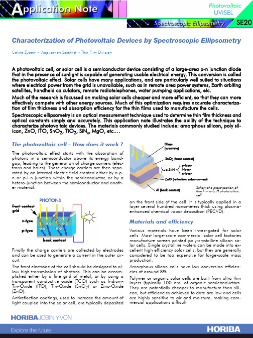
Characterization of Photovoltaic Devices by Spectroscopic Ellipsometry Céline Eypert - Application Scientist - Thin Film DivisionA photovoltaic cell, or solar cell is a semiconductor device consisting of a large-area p-n junction diode that in the presence of sunlight is capable of generating usable electrical energy. This conversion is called the photovoltaic effect. Solar cells have many applications, and are particularly well suited to situations where electrical power from the grid is unavailable, such as in remote area power systems, Earth orbiting satellites, handheld calculators, remote radiotelephones, water pumping applications, etc.Much of the research is focussed on making solar cells cheaper and more efficient, so that they can more effectively compete with other energy sources. Much of this optimization requires accurate characteriza-tion of film thickness and absorption efficiency for the thin films used to manufacture the cells. Spectroscopic ellipsometry is an optical measurement technique used to determine thin film thickness and optical constants simply and accurately. This application note illustrates the ability of the technique to characterize photovoltaic devices. The materials commonly studied include: amorphous silicon, poly sil-icon, ZnO, ITO, SnO2, TiO2, SiN x, MgO, etc.…The photovoltaic cell – How does it work ?The photovoltaic effect starts with the absorption ofphotons in a semiconductor above its energy band-gap, leading to the generation of charge carriers (elec-trons and holes). These charge carriers are then sepa-rated by an internal electric field created either by a p-n or p-i-n junction within the semiconductor, or by ahetero-junction between the semiconductor and anoth-er material.Finally the charge carriers are collected by electrodes and can be used to generate a current in the outer cir-cuit.The front electrode of the cell should be designed to al-low high transmission of photons. This can be accom-plished either by a fine grid of metal, or by using a transparent conductive oxide (TCO) such as Indium-Tin-Oxide (ITO), Tin-Oxide (SnO2) or Zinc-Oxide (ZnO).Antireflection coatings, used to increase the amount of light coupled into the solar cell, are typically deposited on the front side of the cell. It is typically applied in a layer several hundred nanometers thick using plasma-enhanced chemical vapor deposition (PECVD).Materials and efficiencyVarious materials have been investigated for solar cells. Most large-scale commercial solar cell factories manufacture screen printed poly-crystalline silicon so-lar cells. Single crystalline wafers can be made into ex-cellent high efficiency solar cells, but they are generally considered to be too expensive for large-scale mass production.Amorphous silicon cells have low conversion efficien-cies of around 8%.Polymer or organic solar cells are built from ultra thin layers (typically 100 nm) of organic semiconductors. They are potentially cheaper to manufacture than sili-con, but efficiencies achieved to date are low and cells are highly sensitive to air and moisture, making com-mercial applications difficult.PHOTONS front contactgridn-typep-typeback contactGlass(substrate)SnO2 (front contact)a-Si:Hp-layeri-layern-layerZnO (reflection enhancement)Al (back contact)Schematic cross-section ofthin film a-Si:H photovoltaiccellSE20Photovoltaic device characterization Three examples of samples commonly characterized by spectroscopic ellipsometers are presented below.The analysis were performed using a HORIBA Jobin Yvon UVISEL spectroscopic phase modulated ellipsom-eter controlled by DeltaPsi2 software. Ellipsometric data were acquired at an angle of inci-dence of 70°, across the extended spectral range from 0.6 to 6.5 eV (190 – 2100 nm).Graded microcrystalline silicon layerThe microcrystalline silicon layer is inhomogeneous in depth. The model includes a graded layer (linear func-tion) used to specify one value at the bottom of the lay-er and another one for the layer top.The optical constants of the microcrystalline silicon were represented using a dispersion formula.The result obtained shows the excellent agreement be-tween the model (line) and the experimental data (dots) on the whole spectral range, with χ2 =0.81 (result quality parameter). Inhomogeneous ZnO layerThe sample consists of a ZnO layer deposited on c-Si. T o represent the inhomogeneity in depth of the ZnO layer, a three layer model was used. The sample exhib-its a small roughness on top, and the density of the ZnO increases from the c-Si interface (1st layer) to the top (2nd layer). It provides an increase of the refractive index from the 1st to the 2nd layer.Graded microcrystalline silicon layerc-Si substrate1226 Åc-Si substrateroughnessZnO82.2% ZnO + 17.8% void27 Å508 Å302 ÅThickness Mapping of SiN x layerBy using a motorized XY sample stage and a mapping recipe it is simple to automate the analysis at different positions on the sample. Both thicknesses and optical constants were determined at each points.The mapping shows a variation of SiN x thickness be-tween 600 and 750 Å over the surface of the sample.ConclusionSpectroscopic ellipsometry is an ideal technique to characterize film thicknesses and optical constants for photovoltaic applications. Spectroscopic ellipsometers are also sensitive to the presence of rough overlayer and graded optical constants.The technique provides the advantage to be fast, sim-ple to operate and non-destructive for the characteriza-tion of the samples.SiNx mc-Si substrate∼ 700 ÅT h i s d o c u m e n t i s n o t c o n t r a c t u a l l y b i n d i n g u n d e r a n y c i r c u m s t a n c e s - P r i n t e d i n F r a n c e - 03/2007。
Datasheet中常用英语词汇翻译

106 107 108 地电位 trimmed bandgap 平衡带隙 dropout voltage 压差 large bulk capacitance 大容量电容 circuit breaker 断路器 charge pump 电荷泵
Datasheet 中常用英语词汇翻译 序号 英文术语 中文术语 1 backplane 背板 2 Band gap voltage reference 带隙电压参考 3 benchtop supply 工作台电源 4 Block Diagram 方块图 5 Bode Plot 波特图 6 Bootstrap 自举 7 Bottom FET Bottom FET 8 bucket capcitor 桶形电容 9 chassis 机架 10 Combi-sense Combi-sense 11 constant current source 恒流源 12 Core Sataration 铁芯饱和 13 crossover frequency 交*频率 14 current ripple 纹波电流 15 Cycle by Cycle 逐周期 16 cycle skipping 周期跳步 17 Dead Time 死区时间 18 DIE Temperature 核心温度 19 Disable 非使能,无效,禁用,关断 20 dominant pole 主极点 21 Enable 使能,有效,启用 22 ESD Rating ESD 额定值 23 Evaluation Board 评估板 24 Exceeding the specifications below may result in permanent damage to the device, or device malfunction. Operation outside of the parameters specified in the Electrical Characteristics section is not implied. 超 过下面的规格使用可能引起永 久的设备损害或设备故障。建议不要工作在电特性表规定的参 数范围以外。 25 Failling edge 下降沿 26 figure of merit 品质因数 27 float charge voltage 浮充电压 28 flyback power stage 反驰式功率级 29 forward voltage drop 前向压降
AE中particular插件中英文对照
AE中particular插件中英文对照(一)Emitter(发射器)Particular/sec (粒子/秒)——每秒钟发射粒子的数量。
Emitter Type(发射器类型)——它决定发射粒子的区域和位置。
Point(点)——从一点发射出粒子Box(盒子)—-粒子会从立体盒子中发射出来,(Emitter Size中XYZ是指发射器大小)Sphere(球形)——和Box很像,只不过发射区域是球形Grid(网格)--(在图层中虚拟网格)从网格的交叉点发射粒子Light(灯光)-—(要先新建一个Light Layer)几个Light Layer可以共用一个Particular。
Layer——使用合成中的3D图层生成粒子,Layer Grid—-同上,发射器从图层网格发射粒子,像Grid一样。
Direction(方向)Uniform(统一)——任一粒子发射类型发射粒子时,会向各个方向移动。
Directional(特定方向)——(如枪口喷射)通过调节X、Y、Z Rotation来实现。
Bi—Directional(相反特定方向)——和Directional十分相似,但是向着两个完全相反的方向发射。
通常为180度。
Disc(盘状)—-通常只在两个维度上,形成一个盘形.Outwards (远离中心)——粒子会始终向远离发射点的方向移动。
而Uniform是随机的。
Direction Spread(方向拓展)——可以控制粒子发射方向的区域。
粒子会向整个区域的百分之几运动。
(即粒子发射方向有多宽) Velocity(速度)——粒子每秒钟运动的像素数。
Velocity Random——每个粒子Velocity的随机性会随机增加或者减小每个粒子的Velocity。
Velocity Distribution()—— Velocity from Motion(速度跟随运动)—-粒子在向外运动的同时也会跟随发射器的运动方向运动。
光光转换效率英文
光光转换效率英文介绍光光转换效率英文是指太阳能电池将光能转化为电能的效率。
在太阳能领域,光光转换效率是一个重要的指标,影响着太阳能电池的实际应用和经济效益。
光光转换效率的提高可以有效地提高太阳能电池的性能和产能,加速太阳能产业的发展。
本文将详细探讨光光转换效率的英文表达,包括相关术语和常用表述。
术语及表述在讨论光光转换效率英文之前,先介绍一些与光光转换效率相关的术语: 1. Photovoltaic conversion efficiency:光伏转换效率 2. Incident light:入射光 3. Absorption:吸收 4. Electron-hole pair:电子空穴对 5. Exciton:激子 6. Charge carrier:载流子 7. Energy band gap:能带间隙 8. Open-circuit voltage:开路电压 9. Short-circuit current:短路电流 10. Fill factor:填充因子 11. Power conversion efficiency:功率转换效率光光转换效率的影响因素光光转换效率受多种因素的影响,下面将逐一介绍这些因素及其英文表述。
材料选择1.Band gap engineering:能带调控2.Semiconducting material:半导体材料3.Absorption coefficient:吸收系数4.Doping concentration:掺杂浓度结构设计1.Surface texture:表面处理2.Anti-reflection coating:抗反射涂层3.Tandem structure:串联结构4.Multi-junction solar cells:多结太阳能电池光学特性1.Quantum efficiency:量子效率2.Reflectance:反射率3.Transmittance:透过率4.Light trapping:光捕获电子输运1.Mobility:迁移率2.Diffusion length:扩散长度3.Recombination:复合4.Tunneling effect:隧穿效应界面特性1.Heterojunction:异质结2.Contact resistance:接触电阻3.Interface trap density:界面态密度4.Passivation:表面钝化设备参数1.Open-circuit voltage:开路电压2.Short-circuit current:短路电流3.Fill factor:填充因子4.Power conversion efficiency:功率转换效率提高光光转换效率的方法在太阳能电池领域,提高光光转换效率是一个持续的研究方向。
赛米控丹佛斯电子 Board_93_GB_SKYPER_42_R 数据表

®Adaptor boardIGBT Driver CoreBoard 93 GB SKYPER 42 R Preliminary Data Features•Two output channels •Gold nickel finish •Failure managementTypical Applications*•Adaptor board for SKYPER 42 IGBT drivers in bridge circuits for industrial applications •PCB with gold plating •DC bus up to 1200VFootnotesIsolation test voltage with external high voltage diodeThe isolation test is not performed as a series test at SEMIKRONThe driver power can be expanded to 50µC with external boost capacitorsIsolation coordination in compliance with EN50178 PD2Operating temperature is real ambient temperature around the driver core Degree of protection: IP00This is an electrostatic discharge sensitive device (ESDS), international standard IEC 60747-1, Chapter IX* The specifications of our components may not be considered as an assurance of component characteristics. Components have to be tested for the respective application. Adjustments may be necessary. The use of SEMIKRON products in life support appliances and systems is subject to prior specification and written approval by SEMIKRON. We therefore strongly recommend prior consultation of our staff.Absolute Maximum Ratings SymbolConditionsValuesUnitV s Supply voltage primary 16V Iout PEAK Output peak current 30A Iout AVmax Output average current 150mA f max Max. switching frequency100kHz V CECollector emitter voltage sense across the IGBT1700V V isol IO Isolation test voltage input - output (AC, rms, 2s)4000V V isolPD Partial discharge extinction voltage, rms, Q PD ≤ 10pC1500V V isol12Isolation test voltage output 1 - output 2 (AC, rms, 2s)1500V R Gon min Minimum rating for external R Gon 0.8ΩR Goff min Minimum rating for external R Goff 0.8ΩT op Operating temperature -40...85°C T stgStorage temperature-40 (85)°CCharacteristics SymbolConditionsmin.typ.max.UnitV s Supply voltage primary side 14.41515.6V V i Input signal voltage on / off 15 / 0V V IT+Input treshold voltage HIGH 12.3V V IT-Input threshold voltage (LOW) 4.6V V G(on)Turn on output voltage 15V V G(off)Turn off output voltage-8V t d(on)IO Input-output turn-on propagation time 1.1µs t d(off)IOInput-output turn-on propagation time1.1µsAdaptor Board 93 SKYPER® 42 RTechnical ExplanationsRevision 04------------------------------------------------------------------------------------------------------------------------------------------------------------------------------------------ This Technical Explanation is valid for the following parts:Related documents:Prepared by: Johannes Krapp------------------------------------------------------------------------------------------------------------------------------------------------------------------------------------------ ContentApplication and Handling Instructions (2)Further application support (2)General Description (2)Dimensions (3)PIN Array (3)Setting Dynamic Short Circuit Protection (4)Collector Series Resistance (4)Adaptation Gate Resistors (5)Boost Capacitors (6)Environmental conditions (6)Mounting Notes (6)Please note:All values in this technical explanation are typical values. Typical values are the average values expected in large quantities and are provided for information purposes only. These values can and do vary in different applications. All operating parameters should be validated by user’s technical experts for each application.Application and Handling Instructions▪Please provide for static discharge protection during handling. As long as the hybrid driver is not completely assembled, the input terminals have to be short-circuited. Persons working with devices have to wear a grounded bracelet. Any synthetic floor coverings must not be statically chargeable. Even during transportation the input terminals have to be short-circuited using, for example, conductive rubber. Worktables have to be grounded. The same safety requirements apply to MOSFET- and IGBT-modules.▪Any parasitic inductances within the DC-link have to be minimised. Over-voltages may be absorbed by C- or RCD-snubber networks between main terminals for PLUS and MINUS of the power module.▪When first operating a newly developed circuit, SEMIKRON recommends to apply low collector voltage and load current in the beginning and to increase these values gradually, observing the turn-off behaviour of the free-wheeling diode and the turn-off voltage spikes generated across the IGBT. An oscillographic control will be necessary. Additionally, the case temperature of the module has to be monitored. When the circuit works correctly under rated operation conditions, short-circuit testing may be done, starting again with low collector voltage.▪It is important to feed any errors back to the control circuit and to switch off the device immediately in failure events.Repeated turn-on of the IGBT into a short circuit with a high frequency may destroy the device.▪The inputs of the hybrid driver are sensitive to over-voltage. Voltages higher than V S +0,3V or below -0,3V may destroy these inputs. Therefore, control signal over-voltages exceeding the above values have to be avoided.▪The connecting leads between hybrid driver and the power module should be as short as possible (max. 20cm), the driver leads should be twisted.Further application supportLatest information is available at . For design support please read the SEMIKRON Application Manual Power Modules available at .General DescriptionThe Board 93 GB SKYPER® 42 is an adaptor board for the IGBT module SKiM® 93 (spring contact). The board is paralleling three channels so the SKiM module can be used in half bridge configuration. The board can be customized allowing adaptation and optimization to the used IGBT module.The switching characteristic of the IGBT can be influenced through user settings, e.g. changing turn-on and turn-off speed by variation of R Gon and R Goff. Furthermore, it is possible to adjust the monitoring level and blanking time for the DSCP (see Technical Explanations SKYPER® 42 R).Please note:This technical explanation is based on the Technical Explanations for SKYPER®42 R. Please read the Technical Explanations SKYPER® 42 R before using the Adaptor Board.Dimensions116 PIN ArraySetting Dynamic Short Circuit ProtectionThe Vce formula for the Vce monitoring is described in the technical explanation of SKYPER 42 R. Collector Series ResistanceDesignation Shape SettingR105 MiniMELF (SMD) R VCE*Factory setting: not equippedTOPR205 MiniMELF (SMD) R VCE *Factory setting: not equippedBOTAdaptation Gate ResistorsBoost CapacitorsEnvironmental conditionsPlease refer to the technical explanation of SKYPER 42 R for the environmental conditions.Mounting NotesDISCLAIMERSEMIKRON reserves the right to make changes withoutfurnished in this document is believed to be accurate and reliable. However, no representation or warranty is given and no liability is assumed with respect to the accuracy or use of such information. SEMIKRON does not assume any liability arising out of the application or use of any product or circuit described herein. Furthermore,。
Photovoltaic cell
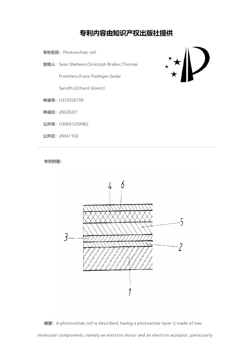
专利名称:Photovoltaic cell 发明人:Sean Shaheen,Christoph Brabec,Thomas
Fromherz,Franz Padinger,Sedar Sariciftci,Erhard Gloetzl 申请号:US10258709 申请日:20020227 公开号:US06812399B2 公开日:2004 1102 专利附图:
Hale Waihona Puke a conjugated polymer component and a fullerene component, and having two metallic electrodes () provided on both sides of the photoactive layer (). In order to provide advantageous construction conditions, it is suggested that an intermediate layer () made of a conjugated polymer, which has doping corresponding to the electrode potential and, in regard to the electron energy, has a band gap between the valence band and the conduction band of at least 1.8 eV, be provided between the photoactive layer () and at least one electrode ().
摘要:A photovoltaic cell is described, having a photoactive layer () made of two molecular components, namely an electron donor and an electron acceptor, particularly
晶硅太阳电池效率提升方向及影响各电性能参数的因素

高丝网印刷太阳电池效率的路径Roadmap to Enhance the Efficiency of a Screen Printed Solar Cell生产程序概况如下:1.初始表面处理与绒面成型(Etching,Cleaning and Texturing Surfaces)2.磷扩散制p/n结与参数测试(Phosphorus Diffusion and Test)3.等离子周边刻蚀与表面腐蚀清洗(Plasma Etching and PSG Chemical Etching)4.减反射膜淀积,钝化与正面电场(Si3N4 Anti-reflection - AR Coating)5.丝网印刷电极和烧结背场(Screen Printing, Sintering and Back Surface Field)6.电池性能测试和分类(Measurement and Sorting)从1970年代至2003年左右,规模化生产太阳能电池的效率最高14%。
低成本、高效率,相互联系,高效率是关键,现在生产18%。
光-电能量转换效率η为:在太阳能电池I-V 特性曲线上作出Rs 和Rsh (ΔV/ΔI = Rs,ΔV/ΔI = Rsh)的图示。
作出最大功率点Pm及表示FF的方框图,写出用I,V表示FF和Pm的公式。
Pm = ImVm = IscVocFF图 p-n结的品质与FF、Rs 和Rsh的关系1.与能量转换效率η相关的参数(The Components of Efficiency)(1)开路电压Voc(Open circuit voltage Voc)式中, Io是无光照时电池的反向饱和电流;q是电子电荷;k是玻尔兹曼常数;T是绝对温度;n是二极管理想因子.(2)短路电流密度Jsc(Short circuit current density Jsc)短路电流Isc:理想状态下,应等于光生电流IL,即Isc=IL 。
光电子学第5章_光电探测器

Yang Jun Photonics Research Center School of Science Harbin Engineering University 2008.12
专业词汇选编
Potodiode
hv Eg
The photodiode is normally reverse biased, the applied reverse bias Vr drops across the highly resistive depletion layer width W and makes the voltage across W equal to Vo+Vr where Vo is the built-in voltage. The field is found by the integration of the net space charge density ρnet across W subject to a voltage difference of Vo+Vr . The field only exists in the depletion region and is not uniform. It varies across penetrates into the n-side. The regions outside the depletion layer are the neutral regions in which there are majority carriers. It is sometimes convenient to treat these neutral regions simply as resistive extensions of electrodes to the depletion layer.
- 1、下载文档前请自行甄别文档内容的完整性,平台不提供额外的编辑、内容补充、找答案等附加服务。
- 2、"仅部分预览"的文档,不可在线预览部分如存在完整性等问题,可反馈申请退款(可完整预览的文档不适用该条件!)。
- 3、如文档侵犯您的权益,请联系客服反馈,我们会尽快为您处理(人工客服工作时间:9:00-18:30)。
Emitter-wrap-through photovoltaic dipole antenna with solar concentratorM.J.Roo Ons,S.V.Shynu,M.J.Ammann,S.J.McCormack and B.NortonA novel photovoltaic dipole antenna employing a solar concentrator as a reflector is proposed.Four identical emitter-wrap-through rear contact solar cells connected in series as a folded dipole are simultaneously used for power generation and as the antenna radiating element,which is located in the focal line of a parabolic solar concentrator.The parabolic structure acts as a solar concentrator for the photovoltaic cells as well as a reflector for the folded dipole antenna.Full-wave elec-tromagnetic simulation with supportive experimental work validates this design.The measured fractional impedance bandwidth and gain were 21%and 11.1dBi,respectively.The antenna /solar arrangement provide a power output of 73.7mW for an irradiance of 1000Wm 22.Introduction:The combination of solar cells and radiating elements into a single device is very attractive in communication systems in order to save space and to reduce installation costs by increasing the potential of emerging compact technologies.It has been shown in space satellite applications that photovoltaic (PV)cells can be located close to micro-strip antennas,avoiding the region where the effective electric fringing field exists [1].The development of thin amorphous silicon technology on flexible polymer substrates enables solar cells to fit into complex antenna geometries,but with lower photovoltaic cell efficiency [2].In recent years increased attention has been focused on the use of polycrys-talline silicon solar cells.They have been used as radiating patches owing to their homogenous metallic rear contact,and also as a ground plane for microstrip antennas [3,4].A new approach in solar antenna design is proposed using a parabolic solar concentrator to increase the illuminated flux on the PV surface,thus reducing the amount of PV material required,and simultaneously acting as an antenna reflector.The electrically conductive emitter-wrap-through (EWT)solar cells are used as antenna elements,where the solar array is connected in series in the form of a folded dipole.A compact decoupling circuit at the dipole feed is used to separate the RF and DC currents.DL1yxzL2ABfocal lineC GG1Fig.1Solar folded dipole with dimensions L1¼85mm,L2¼82mm,D ¼4mm,G ¼5mm,G1¼2mmLtHpLpPa bzB ADC llines 50 W coaxslots CCLLs × WsxyFig.2Solar folded dipole antenna with parabolic reflectora Perspective view of proposed antenna with dimensions Lt ¼205mm,Hp ¼75mm,Lt ¼245mm for parabolic reflector with focal line at P ¼55mmb RF-DC decoupling network with dimensions Ls ¼45mm,Ws ¼1.9mm for slot illustrating balun on 50V lineUse of EWT rear contact solar cell:Conventional crystalline and amor-phous silicon solar cells used so far in solar antenna approaches have contact metallisation on both front and rear surfaces to extract current [5].In the EWT,the front surface of the cells used is devoid of any metallisation so that the complete cell surface is available for light absorption [6].Even though the emitter is located near the front,both negative and positive polarity contacts are placed on the rear surfacewith the negative contact connected to the front through emitter wrapped holes.Consequently,for this type of cell there is no fully covered metallisation on any side,just an interdigitated structure alter-nating positive and negative polarity metal fingers.The RF behaviour was investigated at microwave frequencies and it was found to behave very closely to that of a conducting strip.Antenna design:The proposed folded dipole consists of four identical 40Â3mm rear contact solar cells interconnected in series,as shown in Fig.1.The dimensions of the folded dipole arms are L 1¼85mm and L 2¼82mm,with a feed gap of G ¼5mm.The spacing between the arms is D ¼4mm.The 300V input impedance of the folded dipole is reduced to 200V by the introduction of the parabolic solar con-centrator (see Fig.2a ).A split-coaxial balun is implemented by introdu-cing two identical slots of dimensions Ls ¼45mm and Ws ¼1.5mm on opposite sides of the outer conductor of the semi-rigid Flexiform 402NM 50V coaxial line,as shown in Fig.2b .A 4:1impedance trans-formation is achieved with this balun by adjusting the slot length [7].Since the solar cells in the presented structure are working simul-taneously as power sources and microwave radiating elements,a DC /RF decoupling circuit is necessary,which is integrated into the feed gap of the folded dipole solar antenna.A standard arrangement of chip capacitors and inductors (C ¼100pF,L ¼68nH)is used to isolate the DC and RF,as shown in Fig.2b .The folded solar dipole antenna is then positioned along the focal line of the parabolic concen-trator,with the active side of the cells facing the reflector.The DC con-nection and feedline pass through a 9mm radius hole to the back of the reflector.The design was optimised using a full-wave electromagnetic simu-lator,CST Microwave Studio.For a parabolic trace following the curve z ¼0.005y 2,the vertical distance between the antenna and reflec-tor for a 200V input impedance at the dipole was found to be P ¼55mm.The required parabolic reflector dimensions are Lt .85mm and Hp .55mm for maximum light concentration,but the actual dimensions chosen were Lt ¼205mm and Hp ¼75mm to ensure a minimum gain of 10dBi over the entire band.3M Vikuiti TM Enhanced Specular Reflector Film was used as the conducting reflector surface.The advantage of selecting a folded dipole over an ordinary dipole is the fact that the series connection of solar cells provides addi-tive DC voltages,as well as its broader bandwidth and convenient matching.Results and discussion:The simulated and measured S 11of the pro-posed antenna is shown in Fig.3with good agreement.The measured return loss was found to be greater than 10dB in the frequency range 1.35–1.68GHz,which corresponds to a fractional impedance band-width of 21%.The measured and simulated E-and H-plane normalised radiation patterns for centre frequency are shown in Fig.4.The measured gain at the centre frequency was found to be 11.1dBi with little variation across the band.The front-to-back ratios for the E-and H-planes were better than 27and 30dB respectively.The measured cross-polar rejec-tion is better than 20dB for bothplanes.50–5–10–15S 11, d B–20–25–301.01.52.0frequency, GHz2.53.0Fig.3Simulated and measured S 11plots for proposed EWT dipole antenna ___measurement -----simulationELECTRONICS LETTERS 26th February 2009Vol.45No.5150120900–10–20–20–30–40–100–20–30–40–100–30–400–10–20–30–406030270180180021024015012090270a b2102403003306030300330Fig.4Measured radiation patterns at 1.49GHz a E-plane (zx )___co-polar measurement _Â_cross-polar measurement -----co-polar simulation b H-plane (zy )___co-polar measurement _Â_cross-polar measurement -----co-polar simulationSingle junction silicon solar cells provide approximately 0.5–0.6V,independently of the cell size.The dipole comprising four cells in series realised a voltage of 2.22V.The behaviour of the solar dipole as a power source was investigated by illumination with a Griven INSE 1200MSR metal halide lamp continuous solar simulator.The solar cells face towards the parabolic reflector and a 10%increase in current was achieved where the dipole was placed at the concentrator focal line,in comparison to the standalone dipole directly facing the light.The four cell solar dipole supplies 73.7mW (I ¼33.2mA,V ¼2.22V)at an irradiance of 1000Wm 22for the reflector with 3M Vikuiti ESR film.Conclusions:A novel folded dipole comprising EWT rear contact solar cells with a parabolic solar concentrator reflector is proposed.The full integration of solar cells and antenna in one device where the PV cells act as the RF radiating element is demonstrated.A maximum antenna gain of 11.1dBi is achieved over a 21%bandwidth.The parabolicreflector works simultaneously as an antenna reflector and as a solar con-centrator increasing the current output by 10%.Acknowledgment:This work was supported by Science Foundation Ireland (SFI)and the research support unit of DIT.#The Institution of Engineering and Technology 200917December 2008Electronics Letters online no:20093617doi:10.1049/el:20093617M.J.Roo Ons,S.V.Shynu and M.J.Ammann (School of Electronic and Communications Engineering,Dublin Institute of Technology,Kevin Street,Dublin 8,Ireland )E-mail:mariajose.rooons@student.dit.ieS.J.McCormack and B.Norton (Dublin Energy Lab,Focas Institute,Camden Row,Dublin 8,Ireland )References1Tanaka,M.,Suzuki,Y.,Araki,K.,and Suzuki,R.:‘Microstrip antennas with solar cells for microsatellites’,Electron.Lett.,1996,31,pp.263–2662Vaccaro,S.,Mosig,J.R.,and De Maagt,P.:‘Two advanced solar antenna SOLANT designs for satellite and terrestrial communications’,IEEE Trans.Antennas Propag.,2000,AP-51,(8),pp.2028–20343Bendel, C.,Henze,N.,Weitz,M.,Hofmann,P.,and Kirchhof,J.:‘Investigations on planar antennas with photovoltaic solar cells for mobile communications’.IEEE Int.Symp.on Personal,Indoor and Mobile Radio Communication (PIMRC),2004,Vol.1,pp.622–6264Shynu,S.V.,Roo Ons,M.J.,Ammann,M.J.,McCormack,S.J.,and Norton, B.:‘Inset-fed microstrip patch antenna with integrated polycrystalline photovoltaic solar cell’.Second European Conf.on Antennas and Propagation (EuCAP),Edinburgh,UK,November 20075Lasnier,F.,and Gan Ang,T.:‘Photovoltaic engineering handbook’(CRC Press,1990)6Van Kerschaver,G.,and Beaucarne,G.:‘Back-contact solar cells:a review’,Prog.Photovolt.:Res.Appl.,2006,14,pp.107–1237Makarov,R.,and Ludwig,R.:‘Analytical model of the split-coaxial balun and its application to a linearly polarized dipole or a CP turnstile’,IEEE Trans.Antennas Propag.,2007,AP-55,(7),pp.1909–1918ELECTRONICS LETTERS 26th February 2009Vol.45No.5。