计算DDR3系统内存的功耗
DDR3必读内容介绍DDR3

1.DDR的发展:2003年秋季Intel公布了DDR2内存的发展计划。
而随着当时CPU 前端总线带宽的提高和高速局部总线的出现,内存带宽成为系统越来越大的瓶颈。
处于主流DDR技术已经发展到极至,因此DDR2脱颖而出。
DDR2的实际工作频率是DDR的两倍。
这得益于DDR2内存拥有两倍于标准 DDR内存的4bit预读取能力。
下图为DDR和DDR2预读取能力的对比。
DDR2内存技术最大的突破点其实不在于用户们所认为的两倍于DDR的传输能力,而是在采用更低发热量、更低功耗的情况下(由2.5V降为1.8V),DDR2 可以获得更快的频率提升,突破标准DDR的400MHZ限制。
DDR内存通常采用TSOP芯片封装形式,这种封装形式可以很好的工作在 200MHz上,当频率更高时,它过长的管脚就会产生很高的阻抗和寄生电容,这会影响它的稳定性和频率提升的难度。
这也就是 DDR的核心频率很难突破275MHZ的原因。
而DDR2内存均采用FBGA封装形式。
不同于目前广泛应用的 TSOP 封装形式,FBGA封装提供了更好的电气性能与散热性,为DDR2内存的稳定工作与未来频率的发展提供了良好的保障。
2007年中Intel表示支持DDR3的发展,随后DDR3慢慢走上了历史的舞台,根据由JEDEC协会所制定的规格来看,由技术面来切入DDR3与DDR2的异同点,DDR3拥有高频率低电压的优点,DDR3可以比DDR2运作时省下约30%的电力,速度方面DDR3从800Mbps起跳最高可以至1600Mbps,几乎是DDR2的二倍速度,正因为高传输率的关系,DDR3可以在一个时序(Clock)之中传出8bit的数据,比起DDR2的4bit也是二倍的数据传输量,低电压更是DDR3的优势之一,1.5V 的电压比DDR2的1.8V降低了17%。
下面的图表总结了DDR,DDR2,以及DDR3的一些重要的区别:2、认识内存相关工作流程与参数首先,我们先了解一下内存的大体结构工作流程,这样会比较容量理解这些参数在其中所起到的作用。
lpddr3参数计算表
lpddr3参数计算表LPDDR3(Low Power DDR3)是一种低功耗的DDR3 SDRAM (Synchronous Dynamic Random Access Memory)标准,广泛应用于移动设备和嵌入式系统中。
LPDDR3具有较低的功耗、较高的带宽和较低的延迟,相对于标准的DDR3,更适合于电池供电的移动设备。
LPDDR3的参数计算表包括动态参数和静态参数。
动态参数包括数据速率、预取长度和工作频率。
LPDDR3的数据速率通常以每秒传输的数据位数来表示,例如LPDDR3-1600表示每个时钟周期传输1600Mb的数据。
预取长度表示每个存取周期传输的连续数据字节数。
工作频率则是LPDDR3与设备通信的时钟频率。
静态参数包括地址总线宽度、数据总线宽度、内存容量和电压。
地址总线宽度决定了LPDDR3能够寻址的内存地址数量,数据总线宽度决定了LPDDR3每个存取周期能够传输的数据量。
内存容量表示LPDDR3可以存储的数据量大小,通常以GB为单位。
电压表示LPDDR3的工作电压,通常是1.2V。
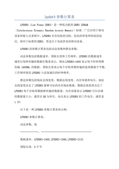
以下是一种LPDDR3参数计算表的示例:LPDDR3参数计算表:动态参数,值-------------,------------------------------------数据速率,LPDDR3-1600,LPDDR3-1866,LPDDR3-2133预取长度,8字节工作频率,800MHz,933MHz,1066MHz静态参数数据总线宽度,32位(每个存取周期传输32位数据)内存容量,1GB,2GB,4GB,8GB电压,1.2V通过LPDDR3参数计算表,我们可以确定LPDDR3内存的具体规格,以便于选型和设计。
参数的选择需要根据具体应用的需求来进行权衡,包括功耗、带宽和容量等方面。
在移动设备和嵌入式系统中,通常需要考虑功耗的优化,因此LPDDR3成为一种较为理想的内存选择。
同时,通过选择合适的数据速率、预取长度和工作频率,可以提供满足应用需求的性能。
ddr3芯片
ddr3芯片DDR3芯片是一种双倍数据速率第三代动态随机存取存储器(DRAM)芯片。
它在电子计算机中扮演着重要的角色,广泛用于个人电脑、服务器、工作站和其他高性能计算设备中。
下面是关于DDR3芯片的介绍,总计1000字。
首先,DDR3芯片是在DDR2芯片的基础上进行了改进和优化的产品。
DDR3芯片的主频可以达到800MHz至2133MHz,从而提供更高的数据传输速度。
这使得计算机可以更快地读取和写入数据,从而提高系统的整体性能和响应速度。
DDR3芯片的工作电压为1.5伏特,相比于之前的DDR2芯片的1.8伏特,功耗更低,能够提供更高的能效。
这在笔记本电脑和其他移动设备中尤其重要,因为它可以延长电池的使用时间。
DDR3芯片采用了更复杂的内部组织结构和电路设计,从而提高了数据传输的稳定性和可靠性。
它引入了8位预取机制,使得每次读写操作可一次传输8个字节的数据,进一步提高了内存的访问速度。
DDR3芯片支持双通道和三通道内存架构,这意味着计算机可以同时访问多个内存模块,并将数据传输分配到不同的通道上,从而提高数据传输的并行性和吞吐量。
这使得DDR3芯片在处理大量数据和多任务处理时表现优秀。
DDR3芯片有着较大的容量范围,从1GB到16GB不等。
这使得计算机可以安装更大容量的内存,进一步提高系统的性能和响应能力。
特别是在高性能应用和大型数据库处理中,DDR3芯片能够提供足够的内存容量来处理大量的数据和运行复杂的应用程序。
此外,DDR3芯片具有良好的兼容性。
它可以与之前的DDR2芯片和之后的DDR4芯片共存,并且可以与各种操作系统和处理器架构配合使用,包括英特尔、AMD和ARM等。
这样,用户可以在不更换整个系统的情况下,仅仅通过更换内存模块来升级和扩展内存容量。
最后,DDR3芯片的价格相对较低,因为它是较早的技术,并且已经有成熟的制造工艺和规模化生产。
这使得DDR3芯片成为广大用户的首选,特别是那些对于性价比有要求的用户。
ad ddr3规则
ad ddr3规则(实用版)目录1.DDR3 内存条的基本概念2.DDR3 内存条的主要特点3.DDR3 内存条的规则4.DDR3 内存条的市场应用正文DDR3 内存条的基本概念DDR3(Double Data Rate 3)是一种内存条(RAM)的标准,用于计算机系统中。
内存条是计算机中用于暂时存储数据和指令的一种硬件设备,当计算机运行时,CPU(中央处理器)会从内存条中读取数据和指令。
内存条的速度和性能对于计算机的整体性能至关重要,而 DDR3 内存条以其高性能和低功耗特性,成为市场上主流的内存条之一。
DDR3 内存条的主要特点DDR3 内存条具有以下主要特点:1.传输速率:DDR3 内存条的传输速率比其前代 DDR2 内存条快很多,最高可达 2666 MT/s(每秒百万次传输)。
2.芯片密度:DDR3 内存条的芯片密度比 DDR2 高,这意味着在同样的物理空间内,DDR3 内存条可以提供更多的内存容量。
3.电压:DDR3 内存条的电压比 DDR2 低,从 1.8V 降至 1.5V,这有助于降低功耗,提高计算机的续航时间。
4.芯片间距:DDR3 内存条的芯片间距比 DDR2 大,这可以降低内存条的制造成本,提高可靠性。
DDR3 内存条的规则DDR3 内存条遵循一些基本规则,包括:1.接口类型:DDR3 内存条通常使用 260-pin SO-DIMM 接口,与 DDR2 的 200-pin SO-DIMM 接口不同。
2.模块容量:DDR3 内存条通常以 1GB、2GB、4GB、8GB 等容量出售,容量越大,价格越高。
3.频率和延迟:DDR3 内存条的频率和延迟是其性能的关键指标。
频率越高,传输速率越快;延迟越低,性能越好。
4.电压:DDR3 内存条的电压应与主板的电压兼容,通常为 1.5V。
DDR3 内存条的市场应用由于其高性能和低功耗特性,DDR3 内存条广泛应用于各种计算机系统,包括:1.台式电脑:DDR3 内存条是台式电脑的主流内存选择,适用于各种办公和娱乐应用。
DDR3和DDR2和DDR的工作原理及技术区别
DDR3和DDR2和DDR的工作原理及技术区别DDR3、DDR2和DDR(又称为DDR1)是计算机系统中常见的内存标准。
它们在工作原理和技术上有一些区别,下面是关于它们的详细介绍。
1. DDR3(Double Data Rate 3):DDR3是一种内存技术标准,它是DDR2的升级版本。
DDR3相比于DDR2有更高的带宽和更低的功耗。
工作原理:DDR3内存的工作原理是在时钟的上升沿和下降沿两个时刻读取数据,因此它被称为双倍数据率。
数据传输速度是时钟速度的两倍,例如DDR3-1600的内存模块实际传输速度为3200MB/s。
技术区别:-电压:DDR3的工作电压为1.5V,比DDR2的电压低,可以节省功耗并降低发热。
-带宽:DDR3的带宽比DDR2更高。
DDR2的带宽是每个内存信号线上每个时钟周期传输的位数乘以时钟速度,而DDR3通过使用更高的时钟速度和每个时钟周期传输的字节大小来提高带宽。
-寻址能力:DDR3的寻址能力比DDR2更高,可以支持更大的内存容量。
-内存频率:DDR3支持更高的内存频率,从800MHz到2133MHz以上。
2. DDR2(Double Data Rate 2):DDR2是DDR的升级版,它具有更高的频率、更低的功耗和更高的密度。
工作原理:DDR2内存也是在上升沿和下降沿两个时刻读取数据,实现双倍数据率传输。
技术区别:-电压:DDR2的工作电压为1.8V,比DDR的电压低,能够降低功耗。
-带宽:DDR2的带宽比DDR更高。
DDR2使用更高的频率和每个时钟周期传输的字节大小来提高带宽。
-寻址能力:DDR2具有更高的寻址能力,能够支持更大的内存容量。
-内存频率:DDR2的内存频率从400MHz到1066MHz。
3. DDR(Double Data Rate):DDR是首个双倍数据率内存技术的标准,它在之前的SDRAM的基础上提高了数据传输速率和带宽。
工作原理:DDR内存是在上升沿读取数据。
ad ddr3规则
ad ddr3规则一、什么是DDR3内存DDR3(Double Data Rate 3)是一种计算机内存标准,它是DDR2内存的后继者。
DDR3内存在传输速度、能耗和容量方面都有了显著的改进。
它是目前主流的计算机内存类型之一。
二、DDR3内存规则DDR3内存有一些规则和要求,下面将详细介绍这些规则。
1. 内存插槽DDR3内存需要插入主板上的内存插槽中。
在插入之前,需要确保内存插槽和内存条的插槽类型匹配。
通常,DDR3内存使用240针的插槽。
2. 内存容量DDR3内存的容量可以根据需求选择,常见的容量有2GB、4GB、8GB等。
在选择内存容量时,需要考虑操作系统和应用程序的需求,以及主板的支持能力。
3. 内存频率DDR3内存的频率也是一个重要的参数。
频率越高,内存的数据传输速度越快。
常见的DDR3内存频率有1333MHz、1600MHz等。
在选择内存频率时,需要根据主板的支持能力和处理器的兼容性来确定。
4. 内存时序DDR3内存的时序参数也需要注意。
时序参数包括CL(CAS Latency)、tRCD(RAS to CAS Delay)、tRP(RAS Precharge Delay)等。
这些参数决定了内存的响应速度和稳定性。
一般来说,时序参数越小,内存性能越好,但也需要注意与主板和处理器的兼容性。
三、DDR3内存的优势DDR3内存相比于前代的内存标准有许多优势。
1. 更高的传输速度DDR3内存采用了更高的频率和更低的供电电压,使得数据传输速度更快。
这对于处理大量数据的应用程序和游戏来说非常重要。
2. 更低的能耗DDR3内存相比于DDR2内存,能耗更低。
这意味着在相同的工作负载下,DDR3内存的功耗更少,从而延长了电池续航时间。
3. 更大的容量支持DDR3内存支持更大的容量,这对于运行内存要求较高的应用程序和虚拟化环境非常重要。
更大的容量可以提供更好的性能和稳定性。
4. 更好的兼容性DDR3内存具有良好的兼容性,可以与各种主板和处理器配合使用。
分析DDR3内存
分析DDR3内存与DDR2相比,DDR3内存将工作在更高的频率下,这也意味着更快的数据传输速度和整机系统性能的又一次提升。
除此之外,DDR3内存还有低功耗的优点,其访问延迟也比DDR2内存有了可观的下降。
在产业界都做好准备的情况下,DDR3内存将会逐渐切入市场,并在未来的1~2年内完成向主流市场的过渡。
有意思的是,与英特尔前卫的作风不同,AMD似乎并不愿意冒推广新技术的风险,但它也宣布将在2008年实现对DDR3内存的支持,届时DDR2很有可能被提前终结,DDR3毋庸置疑将成为内存市场新的主导力量。
内存技术的回顾与发展在PC发展历史中,CPU速度与内存速度总是在交替中提升,两者的关系也密不可分。
CPU运算所需的所有数据都来自于内存,同样,CPU运算生成的数据也必须存放在内存,如果内存速度跟不上,那么CPU就会浪费很多时间在数据等待上面,这不可避免影响了CPU 性能的发挥。
正因为如此,CPU与内存总是捆绑在一起构成一套“运算子系统(平台)”,而这个“平台”的升级也往往是以内存规格的升级为主要标志的。
想当初,DDR2内存从2003年开始切入市场,第一代DDR发展到400MHz便嘎然而止,尽管内存厂商能够量产出500MHz甚至更高频率的产品,但JEDEC并没有考虑对DDR规范进行扩充,而是直接转入DDR2体系。
DDR2标准同样是从400MHz起步,分别为DDR2 400、DDR2 533、DDR2 667和DDR2 800。
但由于DDR2的访问延迟比DDR多了几个周期,导致DDR2 400和DDR2 533内存都没有表现出比DDR 400更好的性能优势;直到DDR2 667之后,更高的时钟频率有效缩短了内存的整体延迟,同时带宽的提升也在应用中表现出明显的性能增益,此时的DDR2才被大规模接受,事实上我们也可以认为DDR2的时代是从DDR2 667开始的。
目前业界正在向DDR2 800过渡,英特尔和AMD平台都可以良好支持DDR2 800。
SDRAM功耗计算
sdram/ddr 功耗计算标签:工作存储嵌入式百度测试2012-04-18 22:58 4907人阅读评论(5) 收藏举报分类:硬件(151)版权声明:本文为博主原创文章,未经博主允许不得转载。
在进行嵌入式系统设计过程中总功耗的计算是一个无法绕开的问题,在总功耗的计算过程中尤其以SDRAM、DDR、DDR2等动态随机存储器件的功耗难以把握和计算。
本人在进行电源IC选型时采用估算措施,一般嵌入式系统总电流不会超过400mA,所以选择电源IC只要在500mA以上即可;电子工程师在选电源IC计算系统总功耗时,总是会在计算DRAM器件功耗时难以下手而不得不对其进行估算。
本人本着将革命进行到底的精神,在闲暇时间百度一些相关资料后进行了学习总结。
1.DDR功耗计算现以DDR为例进行功耗计算,此过程可以推广到SDRAM和DDR2功耗计算。
DRAM器件功耗难以准确计算的原因是由于该类器件工作状态繁多,且系统运行过程这些状态还不断切换,这些都为功耗的计算造成了阻碍。
具体计算内存的功耗不是很容易的事,我们计算的结果只是一个假定工作条件下的平均值。
为了估算内存芯片功耗,首先必须了解芯片的一些基本功能,下图是DDR功能模块图:从上图可以看到,每个BANK都有一个SENSE AMPLIRERS(读出放大器),在进行读、写、自动刷新等操作时,需要先把存储阵列中的数据进行缓存后才能进行操作,SENSE AMPLIRERS就是这个缓存器。
DDR大致有以下几种工作状态,特总结如下:ACTIVE(激活)、Precharge(预充电)、读、写、自动刷新、自刷新ACTIVE(激活)用简单的一句话来描述,激活命令的作用就是将选择地址的bit信号送入读出放大器,以供下一步的读或写做准备。
从字面上来理解,就是将存储矩阵电路中位信号发送到读出放大器以供外设使用,也就是将存储信号激活。
预充电(Precharge)指关闭所有行地址线(rowline),所有列地址线(bitline)接1/2Vcc源经过足够长时间冲或放电使列地址电容电压值达到1/2VCC的动作。
ddr3工作原理

ddr3工作原理
DDR3(Double Data Rate 3)是一种电脑内存标准,与早期的DDR(DDR1)和DDR2相比,DDR3具有更高的频率、更低
的功耗和更高的数据传输速度。
DDR3工作原理如下:
1. 现场二进制编码(BL,Burst Length):DDR3内存以8位
为编码单元,每次传输的数据长度通常为8位或64位。
传输
长度的设置可以在读写命令中进行调整,以适应不同的访问需求。
2. 频率倍增(Double Data Rate):DDR3内存通过在每个时钟周期的上升和下降沿传递数据,从而实现了数据传输速度的翻倍。
这意味着DDR3内存在与系统总线通信时,每个时钟周
期可以传输两个数据位,从而提高了整体数据传输效率。
3. 预充电和负载(Precharge and Load):DDR3内存模块在发
送数据之前,首先要将内部触发器的电平预充电至一定的电压。
预充电后,内存模块可以更快地从内部电容中加载数据,从而减少了延迟时间。
4. 自适应写时延调整(Adaptive Write Latency Adjustment):DDR3内存会根据当前的操作模式和数据传输需求自动调整写
时延。
这样可以确保数据的稳定传输,同时减少了写操作的等待时间。
5. 数据校验和纠错(Error Checking and Correction,ECC):
一些DDR3内存模块支持ECC技术,可以检测和纠正内存的
错误。
ECC功能通过添加冗余校验位来实现,确保数据在传输过程中的准确性和完整性。
通过以上的工作原理,DDR3内存可以实现更高的数据传输速度和稳定性,从而提升计算机的整体性能。
DDR3内存深度解析

DDR3内存深度解析2007年第⼆季度开始,DDR3平台就会全⾯启动。
从去年开始,全球各⼤内存芯⽚⼚商已经陆续推出DDR3颗粒,在今年秋季IDF展会上已经出现⽐较成熟的DDR3内存模组,估计明年开始将⼤量投⼊⽣产。
另⼀⽅⾯,全球最⼤的主板芯⽚供应商Intel 已经在蓝图上公布明年第⼆季度就会推出⽀持DDR3内存的新平台,看来草船、东风皆备,内存终于再次⾯临更新换代。
DDR2内存技术简单回顾 IT业界的正式内存规格是由JEDEC-- Joint Electronioc Device Engineering Council制定的,这包括了DDR、DDR2以及准备推出的DDR3,在官⽅规格中DDR最⾼速度为DDR400,但由于制程进步,DDR的速度已经完全超越了官⽅原定标准,故此后期出现了超⾼速DDR566并⾮官⽅规格。
继DDR400之后,JEDEC已认定DDR2为现时主流内存标准,虽然名字上只差毫厘,但DDR2和DDR2是完全不兼容的,⾸先DDR2的为240Pin接⼝⽐DDR的184Pin长,另外电压也⽐DDR的2.5v低许多,在1.8v的同频率下DDR2可⽐DDR低⼀半功耗,⾼频低功耗是DDR2内存的优点,⽽缺点则是DDR的延迟值⽐较⾼,在同频率下效能较低。
不单在规格上不兼容,其实DDR和DDR2在技术上有很⼤分别。
我们⽤的内存是透过不停充电及放电的动作记录数据的,上代SDRAM内存的核⼼频率就相等于传送速度,⽽每⼀个Mhz只会有传送1 Bit的数据,采⽤1 Bit Prefetch。
故此SDRAM 100Mhz的频宽为100Mbps。
但随着系统内部组件速度提升,对内存速度的要求增加,单纯提升内存频率已经不能应付需求,幸好及时发展出DDR技术。
DDR与SDRAM的分别在于传统SDRAM只能于充电那⼀刻存取数据,故此每⼀下充电放电的动作,只能读写⼀次,⽽DDR却把技术提升⾄在充电及放电时都能存取数据,故此每Mhz有两次存取动作,故此DDR会⽐SDRAM在同⼀频率下效能提⾼⼀倍,⽽100Mhz的DDR却可达⾄200Mbps存取速度,由于每⼀个Mhz都要有⼆次的资料存取,故此DDR每⼀Mhz会传送2Bit,称为2Bit Prefetch,⽽DDR颗粒频率每提升1Mhz,所得的效果是SDRAM的两倍。
ddr3读写时序描述、数据吞吐量与ddr3容量计算方式
ddr3读写时序描述、数据吞吐量与ddr3容量计算方式DDR3 is a type of synchronous dynamic random-access memory (SDRAM) that is commonly used in computer systems. It operates at a higher clock speed compared to DDR2, which allows for increased data transfer rates. In this discussion, we will explore the description of DDR3read/write timing, the calculation of its data throughput, and how to determine its capacity.DDR3读写时序描述DDR3的读写时序是指内存模块在数据传输过程中所遵循的时间规则。
它涉及到如下几个关键参数:CAS latency (CL),RAS-to-CASdelay (tRCD),RAS Precharge time (tRP),以及RAS Activetime (tRAS)。
1. CAS Latency(CL): 它表示从列地址被访问到数据开始输出的延迟时间。
较低的CAS latency值意味着内存响应更快,但会增加功耗和稳定性要求。
2. RAS-to-CAS Delay(tRCD): 这是指行地址被访问后多久才能开始访问列地址。
较低的tRCD值可提高内存性能。
3. RAS Precharge Time(tRP): 它表示在 RAS 操作之后行被关闭所需的时间。
较低的 tRP 值可以提高内存效率和性能。
4. RAS Active Time(tRAS): 行保持激活状态的时间。
越长,内存性能和吞吐量越好,但同时会增加功耗。
c6678 ddr3倍频和分频参数
c6678 ddr3倍频和分频参数随着计算机技术的不断发展,内存条的性能对于计算机整体性能的影响越来越大。
在众多内存条型号中,DDR3内存以其高速度、高容量和稳定性受到了用户的喜爱。
本文将详细介绍DDR3内存的倍频和分频参数,帮助大家更好地了解和选择适合自己的DDR3内存。
一、DDR3内存概述DDR3(Double Data Rate 3)内存是一种第三代双倍数据传输率内存,相较于前代产品DDR2,DDR3内存具有更高的传输速率和更低的功耗。
它采用了On-die termination(ODT)技术,使得信号传输更加稳定。
此外,DDR3内存还支持多种电压版本,如1.5V、1.35V和1.0V等。
二、DDR3倍频和分频的含义1.倍频:倍频是指内存模块的工作频率,即内存模块每秒钟可以进行多少次数据传输。
DDR3内存的倍频范围为400-2133MHz。
倍频越高,内存的传输速率越快,但同时也可能导致更高的功耗和发热。
2.分频:分频是指内存控制器与内存模块之间的数据传输速率比例。
分频值越小,内存控制器与内存模块之间的数据传输速率越接近,性能越好。
但分频过低可能导致内存带宽浪费,因此需要在实际应用中根据需求进行合理选择。
三、DDR3倍频和分频的计算方法DDR3内存的倍频和分频计算方法如下:1.倍频计算:内存模块的倍频等于内存控制器的工作频率除以2。
例如,当内存控制器工作频率为1066MHz时,内存模块的倍频为1066MHz / 2 = 533MHz。
2.分频计算:分频值等于内存控制器的工作频率除以内存模块的倍频。
例如,当内存控制器工作频率为1066MHz,内存模块倍频为533MHz时,分频值为1066MHz / 533MHz = 2。
四、DDR3倍频和分频参数的实用意义1.匹配性能:合理选择倍频和分频参数,可以使内存控制器与内存模块达到较高的传输速率,提高计算机整体性能。
2.系统稳定性:合适的倍频和分频参数有助于降低内存模块与控制器之间的信号衰减,提高系统稳定性。
内存条ddr3和ddr4的区别
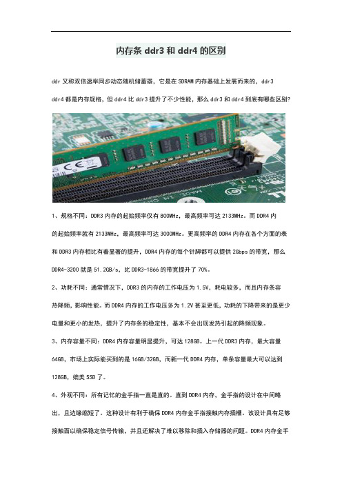
内存条ddr3和ddr4的区别ddr又称双倍速率同步动态随机储蓄器,它是在SDRAM内存基础上发展而来的,ddr3ddr4都是内存规格,但ddr4比ddr3提升了不少性能,那么ddr3和ddr4到底有哪些区别?1、规格不同:DDR3内存的起始频率仅有800MHz,最高频率可达2133MHz。
而DDR4内的起始频率就有2133MHz,最高频率可达3000MHz。
更高频率的DDR4内存在各个方面的表和DDR3内存相比有着显著的提升,DDR4内存的每个针脚都可以提供2Gbps的带宽,那么DDR4-3200就是51.2GB/s,比DDR3-1866的带宽提升了70%。
2、功耗不同:通常情况下,DDR3的内存的工作电压为1.5V,耗电较多,而且内存条容热降频,影响性能。
而DDR4内存的工作电压多为1.2V甚至更低,功耗的下降带来的是更少电量和更小的发热,提升了内存条的稳定性,基本不会出现发热引起的降频现象。
3、内存容量不同:DDR4内存容量明显提升,可达128GB。
上一代DDR3内存,最大容量64GB,市场上实际能买到的是16GB/32GB,而新一代DDR4内存,单条容量最大可以达到128GB,媲美SSD了。
4、外观不同:所有记忆的金手指一直是直的。
直到DDR4内存,金手指的设计在中间略出,且边缘缩短了。
这种设计有利于确保DDR4内存金手指接触内存插槽。
该设计具有足够接触面以确保稳定信号传输,并且还解决了难以移除和插入存储器的问题。
DDR4内存金手中间的凹口(防呆口)比DDR3更靠近中间。
这意味着,DDR4内存不再兼容DDR3,老平台电法升级DDR4内存,除非将CPU和主板都更换为新平台。
ddr3协议规范文档
ddr3协议规范文档DDR3 协议规范概述DDR3(双倍数据率 3)是一种用于计算机主内存的高速动态随机存取存储器(DRAM)技术。
它在 DDR2 技术的基础上进行改进,以提供更快的速度、更低的功耗和更高的容量。
速度和性能DDR3 的数据传输速率比 DDR2 快一倍,达到 800 MHz。
它还采用了突发访问模式,允许一次传输多个相邻数据块,进一步提高了性能。
功耗DDR3 针对低功耗进行了优化,具有多种功耗节能功能。
它允许使用部分阵列自刷新(PAR)和温度补偿自刷新(TCR),以在不需要时关闭阵列部分或降低刷新速率。
容量DDR3 支持高达 8GB 的单条容量,比 DDR2 的 4GB 容量有所增加。
这允许更快的内存容量扩展和更高的系统性能。
时序和命令DDR3 使用一个称为 JEDEC 标准的时序规范,定义了内存模块和内存控制器之间的通信。
它还引入了新的命令,例如 WRITE TO PRECHARGE(WTP),以提高突发访问的效率。
DRAM 结构DDR3 采用与 DDR2 相同的基本 DRAM 单元结构。
它由存储单元、行和列选通器以及输入/输出缓冲器组成。
不过,DDR3 中的存储单元经过重新设计,具有更低的电容,从而可以实现更高的速度。
电源管理DDR3 具有一个称为自适应接口电源管理(AIPM)的电源管理系统。
AIPM 允许内存模块根据系统的负载和活动水平调节其电源消耗。
封装和引脚数DDR3 模块通常采用 DIMM(双列直插式内存模块)封装,具有240 个引脚。
DIMM 由一个连接器连接到主板上的内存插槽。
兼容性DDR3 内存模块与 DDR2 内存插槽不兼容。
因此,在 DDR2 系统中无法使用 DDR3 模块,反之亦然。
应用DDR3 主要用于个人计算机、服务器和嵌入式系统。
它提供了高速、低功耗和高容量的内存解决方案,可满足现代计算应用程序的苛刻要求。
SDRAM功耗计算分析
sdram/ddr 功耗计算标签:工作存储嵌入式百度测试2012-04-18 22:58 4907人阅读评论(5) 收藏举报分类:硬件(151)版权声明:本文为博主原创文章,未经博主允许不得转载。
在进行嵌入式系统设计过程中总功耗的计算是一个无法绕开的问题,在总功耗的计算过程中尤其以SDRAM、DDR、DDR2等动态随机存储器件的功耗难以把握和计算。
本人在进行电源IC选型时采用估算措施,一般嵌入式系统总电流不会超过400mA,所以选择电源IC只要在500mA以上即可;电子工程师在选电源IC计算系统总功耗时,总是会在计算DRAM器件功耗时难以下手而不得不对其进行估算。
本人本着将革命进行到底的精神,在闲暇时间百度一些相关资料后进行了学习总结。
1.DDR功耗计算现以DDR为例进行功耗计算,此过程可以推广到SDRAM和DDR2功耗计算。
DRAM器件功耗难以准确计算的原因是由于该类器件工作状态繁多,且系统运行过程这些状态还不断切换,这些都为功耗的计算造成了阻碍。
具体计算内存的功耗不是很容易的事,我们计算的结果只是一个假定工作条件下的平均值。
为了估算内存芯片功耗,首先必须了解芯片的一些基本功能,下图是DDR功能模块图:从上图可以看到,每个BANK都有一个SENSE AMPLIRERS(读出放大器),在进行读、写、自动刷新等操作时,需要先把存储阵列中的数据进行缓存后才能进行操作,SENSE AMPLIRERS就是这个缓存器。
DDR大致有以下几种工作状态,特总结如下:ACTIVE(激活)、Precharge(预充电)、读、写、自动刷新、自刷新ACTIVE(激活)用简单的一句话来描述,激活命令的作用就是将选择地址的bit信号送入读出放大器,以供下一步的读或写做准备。
从字面上来理解,就是将存储矩阵电路中位信号发送到读出放大器以供外设使用,也就是将存储信号激活。
预充电(Precharge)指关闭所有行地址线(rowline),所有列地址线(bitline)接1/2Vcc源经过足够长时间冲或放电使列地址电容电压值达到1/2VCC的动作。
ddr3电气参数
DDR3电气参数1. 什么是DDR3?DDR3(Double Data Rate 3)是一种电脑内存标准,是DDR2的后继者。
它是一种同步动态随机存取存储器(SDRAM),用于提供计算机系统所需的临时存储。
DDR3内存模块使用184引脚的DIMM(双列直插式内存模块)封装,其电气参数对于DDR3内存的性能和稳定性至关重要。
2. DDR3电气参数的重要性DDR3电气参数是指内存模块在工作过程中的电气特性,包括电压、时序、噪声等。
这些参数对于内存模块的性能、稳定性和兼容性非常重要。
通过合理设置和控制DDR3电气参数,可以确保内存模块在各种工作负载下的稳定性和可靠性。
同时,了解和理解DDR3电气参数也有助于优化内存性能,提高计算机系统的整体性能。
3. DDR3电气参数的详细解析3.1 电压(Voltage)DDR3内存模块的标准电压为1.5V,但也有低电压版本的DDR3内存模块,其电压为1.35V。
电压是内存模块工作所需的电力,合适的电压水平对于内存的稳定性和功耗都有重要影响。
3.2 时序(Timing)时序是指内存模块在读取和写入数据时的时钟信号和延迟时间。
DDR3内存模块的时序参数包括CAS延迟(CL)、RAS到CAS延迟(tRCD)、RAS预充电时间(tRP)等。
合理设置时序参数可以提高内存模块的响应速度和数据传输效率,但过高的时序参数可能会导致内存模块的稳定性下降。
3.3 带宽(Bandwidth)带宽指的是内存模块在单位时间内能够传输的数据量。
DDR3内存模块的带宽与时钟频率、数据位宽和读写命令等因素相关。
较高的带宽可以提高计算机系统的数据处理能力,提升性能。
3.4 噪声(Noise)DDR3内存模块在工作过程中会产生一定的噪声,包括电磁干扰、串扰等。
合理设计内存模块的布局和电路结构,以及使用屏蔽和隔离技术,可以有效减少噪声对内存模块性能的影响。
3.5 内存容量(Capacity)DDR3内存模块的容量可以根据需求选择,常见的容量有2GB、4GB、8GB等。
SDRAM功耗计算
sdram/ddr 功耗计算标签:工作存储嵌入式百度测试2012-04-18 22:58 4907人阅读评论(5) 收藏举报分类:硬件(151)版权声明:本文为博主原创文章,未经博主允许不得转载。
在进行嵌入式系统设计过程中总功耗的计算是一个无法绕开的问题,在总功耗的计算过程中尤其以SDRAM、DDR、DDR2等动态随机存储器件的功耗难以把握和计算。
本人在进行电源IC选型时采用估算措施,一般嵌入式系统总电流不会超过400mA,所以选择电源IC只要在500mA以上即可;电子工程师在选电源IC计算系统总功耗时,总是会在计算DRAM器件功耗时难以下手而不得不对其进行估算。
本人本着将革命进行到底的精神,在闲暇时间百度一些相关资料后进行了学习总结。
1.DDR功耗计算现以DDR为例进行功耗计算,此过程可以推广到SDRAM和DDR2功耗计算。
DRAM器件功耗难以准确计算的原因是由于该类器件工作状态繁多,且系统运行过程这些状态还不断切换,这些都为功耗的计算造成了阻碍。
具体计算内存的功耗不是很容易的事,我们计算的结果只是一个假定工作条件下的平均值。
为了估算内存芯片功耗,首先必须了解芯片的一些基本功能,下图是DDR功能模块图:从上图可以看到,每个BANK都有一个SENSE AMPLIRERS(读出放大器),在进行读、写、自动刷新等操作时,需要先把存储阵列中的数据进行缓存后才能进行操作,SENSE AMPLIRERS就是这个缓存器。
DDR大致有以下几种工作状态,特总结如下:ACTIVE(激活)、Precharge(预充电)、读、写、自动刷新、自刷新ACTIVE(激活)用简单的一句话来描述,激活命令的作用就是将选择地址的bit信号送入读出放大器,以供下一步的读或写做准备。
从字面上来理解,就是将存储矩阵电路中位信号发送到读出放大器以供外设使用,也就是将存储信号激活。
预充电(Precharge)指关闭所有行地址线(rowline),所有列地址线(bitline)接1/2Vcc源经过足够长时间冲或放电使列地址电容电压值达到1/2VCC的动作。
计算DDR3系统内存的功耗
计算DDR3系统内存的功耗
DDR3系统内存的功耗是指在使用中所消耗的电力。
系统内存的功耗是由多个因素决定的,例如内存的容量、时钟频率、电压和工作模式等。
首先,内存的容量是影响功耗的重要因素之一、一般来说,内存容量越大,功耗也越高。
这是因为更多的存储单元需要更多的电能来驱动。
例如,Kbyte级别的内存功耗通常低于Gbyte级别的内存功耗。
其次,内存的时钟频率也会直接影响功耗。
时钟频率越高,每个时钟周期需要更多能量来工作,从而增加了内存的功耗。
内存的时钟频率通常以MHz或GHz为单位进行标识。
对于DDR3内存,常见的时钟频率包括800MHz、1066MHz、1333MHz等。
此外,内存的电压也是影响功耗的因素之一、内存的工作电压通常以伏特为单位进行标识。
DDR3内存的标准工作电压为1.5V,但也有低电压版本的DDR3内存,其工作电压为1.35V。
较低的电压可以降低内存的功耗,但也可能降低内存的性能。
最后,内存的工作模式也会对功耗产生影响。
一般来说,内存可以在不同的模式下工作,例如活动模式和休眠模式。
在活动模式下,内存需要持续地接收和发送数据,功耗相对较高。
而在休眠模式下,内存则可以降低功耗,但也无法进行数据的读写操作。
综上所述,DDR3系统内存的功耗受多个因素的影响,包括内存的容量、时钟频率、电压和工作模式等。
具体的功耗数值需要根据实际情况进行测量和计算。
在选择内存时,可以根据功耗要求进行合理的选择,以平衡性能和功耗之间的关系。
电脑主机功耗计算公式
电脑主机功耗计算公式电脑主机功耗这事儿啊,听起来可能有点复杂,但其实搞清楚了也不难。
咱们先来说说电脑主机里那些耗电的家伙。
CPU 算是个“电老虎”,不同型号、不同工作状态下,它的功耗差别可不小。
比如说,当你在玩大型游戏,让CPU 全力工作的时候,它消耗的电可比只是浏览网页、处理文档的时候多得多。
还有显卡,这也是个吃电的大户。
特别是那些高端显卡,玩起 3A大作来,那功率呼呼地往上涨。
主板呢,虽然单个看起来耗电不多,可也不能小瞧。
上面的各种芯片、电路,都在悄悄地消耗着电能。
内存、硬盘这些相对来说耗电少点,但也不是不耗电。
那怎么计算电脑主机的功耗呢?其实有个简单的办法,就是把各个硬件的典型功耗加起来。
比如说,你的 CPU 典型功耗是 65 瓦,显卡是 150 瓦,主板 30 瓦,内存 10 瓦,硬盘 10 瓦,这样加起来就是 65 + 150 + 30 + 10 + 10 = 265 瓦。
但这只是个大概的数,实际使用中可能会有上下浮动。
我之前帮朋友装电脑的时候,就特别在意功耗这事儿。
他预算有限,又想要性能不错的电脑,还想省电。
我就给他精心挑选了低功耗但性能也还可以的硬件。
像 CPU 选了个能耗比不错的型号,显卡也是找了个功耗不太高但能满足他游戏需求的。
装完之后,我用软件测了一下实际功耗,跟我之前计算的差不多。
朋友可高兴了,说既省钱又省电,还能愉快地玩游戏。
不过要注意,电脑在不同的工作负载下,功耗是会变化的。
比如说,你同时开着好几个大型程序,或者进行视频渲染,这时候功耗就会比平时高很多。
所以啊,在选择电源的时候,不能只按照刚刚计算出来的那个数字来,要留一定的余量,免得电源过载出问题。
总之,计算电脑主机功耗,既能帮我们了解电脑的用电情况,也能在装机的时候合理选择电源,避免浪费或者不够用的情况。
希望大家都能算清楚自己电脑主机的功耗,让电脑高效又省电地为我们服务!。
电脑怎么算功耗

电脑功耗计算原理及方法电脑作为现代人们工作、学习和娱乐的重要工具,功耗问题一直备受关注。
计算机功耗是指在运行过程中消耗的电能,它与硬件配置、使用时间和负载程度等因素密切相关。
正确计算电脑功耗有助于合理规划能源使用,降低能源浪费,本文将介绍电脑功耗的计算原理及方法。
电脑功耗计算原理电脑整体功耗由两部分组成:静态功耗和动态功耗。
静态功耗是指电脑在空闲状态下的能耗,主要来自于主板、内存、硬盘等组件;动态功耗则是指在电脑运行时处理器、显卡等组件产生的功耗,它随着负载的增加而增加。
通常情况下,动态功耗占据电脑整体功耗的大部分。
电脑功耗计算方法1. 使用电表测量法最简单的方法是使用电表来测量电脑的功耗。
首先,将电脑插入电表中,记录初始功耗数值;然后,让电脑运行一段时间,记录结束时的功耗数值。
两者之差即为电脑在该时段的功耗。
这种方法简单易行,但并不精确。
2. 软件监测法另一种方法是通过软件来监测电脑的功耗。
有一些专门的软件工具可以实时监测电脑的功耗情况,用户可以通过这些软件来获取电脑在不同负载下的功耗数值。
这种方法相对准确,但可能会受软件本身的影响。
3. 硬件监测法最精确的方法是使用专门的功耗监测设备来监测电脑的功耗。
这些设备通常连接在电脑的电源线上,可以实时监测电脑整体的功耗情况。
虽然这种方法价格较高且操作复杂,但可以提供最为准确的功耗数据。
总结电脑功耗的准确计算对于能源的合理利用至关重要。
通过了解电脑功耗的计算原理及方法,用户可以更好地了解电脑的能耗情况,从而采取相应的节能措施。
希望本文能帮助读者更好地了解电脑功耗相关知识,提高能源利用效率。
- 1、下载文档前请自行甄别文档内容的完整性,平台不提供额外的编辑、内容补充、找答案等附加服务。
- 2、"仅部分预览"的文档,不可在线预览部分如存在完整性等问题,可反馈申请退款(可完整预览的文档不适用该条件!)。
- 3、如文档侵犯您的权益,请联系客服反馈,我们会尽快为您处理(人工客服工作时间:9:00-18:30)。
Technical NoteCalculating Memory System Power for DDR3IntroductionDDR3 SDRAM provides additional bandwidth over previous DDR and DDR2 SDRAM. Inaddition to the premium performance, DDR3 has a lower operating voltage range. Theresult can be a higher bandwidth performing system while consuming equal or lesssystem power. However, it is not always easy to determine the power consumptionwithin a system application from the data sheet specification.This technical note details how DDR3 SDRAM consumes power and provides the toolsthat system designers can use to estimate power consumption in any specific system. Inaddition to offering tools and techniques for calculating system power, Micron’s DDR3-1067 “Data Sheet Specifications” on page20 and a DDR3 Power Spreadsheet UsageExample on page20 are provided.Table1 describes the command abbreviations found in the following sections.Table 1: Abbreviation DefinitionsAbbreviation DefinitionACT ACTIVATEBL Burst lengthBC Burst chopPRE PRECHARGEODT On-die terminationRD READREF REFRESHWR WRITEDRAM OperationTo estimate the power consumption of a DDR3 SDRAM, it is necessary to understand thebasic functionality of the device (see Figure1 on page2). The operation of a DDR3device is similar to that of a DDR2. For both devices, the master operation of the DRAMis controlled by clock enable (CKE).If CKE is LOW, the input buffers are turned off. To allow the DRAM to receive commands,CKE must be HIGH, thus enabling the input buffers and propagates the command/address into the logic/decoders on the DRAM.During normal operation, the first command sent to the DRAM is typically an ACTcommand. This command selects a bank and row address. The data, which is stored inthe cells of the selected row, is then transferred from the array into the sense amplifiers.The portion of the DRAM consuming power in the ACT command is shown in blue andgold in Figure1 on page2.PDF: 09005aef829559ff/Source: 09005aef828dcdbf Micron Technology, Inc., reserves the right to change products or specifications without notice. TN41_01DDR3 Power.fm-Rev. B 8/07 EN©2007 Micron Technology, Inc. All rights reserved.Eight different array banks exist on the DDR3 SDRAM. Each bank contains its own set ofsense amplifiers and can be activated separately with a unique row address. When oneor more banks has data stored in the sense amplifiers, the DRAM is in the active state.The data remains in the sense amplifiers until a PRE command to the same bankrestores the data to the cells in the array. Every ACT command must have a PREcommand associated with it; that is, ACT and PRE commands occur in pairs unless aPRECHARGE ALL command is used.Figure 1: 1Gb DDR3 SDRAM Functional Block DiagramIn the active state, the DDR3 device can perform READs and WRITEs. A READ commanddecodes a specific column address associated with the data that is stored in the senseamplifiers (shown in green in Figure1). The data from this column is driven through theI/O, gating to the internal READ latch. From there, it is multiplexed onto the outputdrivers. The circuits used in this function are shown in purple in Figure1.The process for a WRITE is similar to the READ except the data propagates in the oppo-site direction. Data from the DQ pins is latched into the data receivers/registers and istransferred to the internal data drivers. The internal data drivers then transmit the datato the sense amplifiers through the I/O gating and into the decoded column addresslocation.DDR3, like DDR2, includes ODT on the data I/O pins. This feature is controlled by theODT pin and consumes additional power when activated. The ODT and the outputdriver on DDR3 includes additional mode register settings over previous DRAM toincrease system flexibility and to optimize signal integrity. This power needs to beincluded in total power calculations (see “I/O Termination Power” on page12).DRAM Power CalculatorsThe I DD values referenced in this article are taken from Micron’s preliminary 1Gb DDR3-1067 data sheet, and they are listed in “Data Sheet Specifications” on page20. While thevalues provided in data sheets may differ from between vendors and different devices,the concepts for calculating power are the same. It is important to verify all data sheetparameters before using the information in this article.Methodology OverviewThe following four steps are required to calculate system power:1.Calculate the power subcomponents from the data sheet specifications. (This calcula-tion is denoted as Pds(XXX), where XXX is the subcomponent power.)2.Derate the power based on the command scheduling in the system (Psch[XXX]).3.Derate the power to the system’s actual operating V DD and clock frequency(Psys[XXX]).4.Sum the subcomponents of the system’s operating conditions to calculate the totalpower consumed by the DRAM.Background PowerAs discussed previously, CKE is the master on-off switch for the DRAM. When CKE isLOW, most inputs are disabled. This is the lowest power state in which the device canoperate, and if all banks are precharged, it is specified in the data sheet as I DD2P. If anybank is open, the current consumed is I DD3P. I DD2P has two possible conditions,depending on whether mode register bit 12 is set for a slow or fast power-down exit time.The appropriate I DD2P value should be used for the power calculations based on howthe application sets this mode register.CKE must be taken HIGH to allow the DRAM to receive ACT, PRE, READ, and WRITEcommands. When CKE goes HIGH, commands start propagating through the DRAMcommand decoders, and the activity increases the power consumption. The currentconsumed is specified in the data sheet as I DD2N if all banks are precharged or I DD3N ifany bank is active.Figure2 on page4 shows the typical current usage of a DDR3 device when CKE transi-tions, assuming all banks are precharged. When CKE is HIGH, the device draws amaximum I DD2N of 65mA of current; when CKE goes LOW, that figures drops to anI DD2P of ~10–25mA, depending on how slow or how fast the power-down exit time is. Allof these values assume the DRAM is in the precharged state. Similarly, if the device is inthe active state, it consumes I DD3P current in power-down (CKE = LOW) and I DD3Ncurrent in standby (CKE = HIGH).Figure 2: Effects of CKE on I DD ConsumptionCalculation of the power consumed by a DDR3 device operating in these standby condi-tions is easily completed by multiplying the I DD and the voltage applied to the device,V DD.Pds(PRE_PDN) = I DD2P × V DD(Eq. 1) Pds(PRE_STBY) = I DD2N × V DD(Eq. 2) Pds(ACT_PDN) = I DD3P × V DD(Eq. 3) Pds(ACT_STBY) = I DD3N × V DD(Eq. 4) The data sheet specification for all I DD values is taken at the worst-case V DD, which is1.575V for DDR3. The calculations for maximum DDR3 standby powers using theassumptions in “Data Sheet Specifications” are as follows:Pds(PRE_PDN) = 25mA × 1.575VPds(PRE_PDN) = 39mW(Eq. 5) Pds(PRE_STBY) = 65mA × 1.575VPds(PRE_STBY) = 102mW(Eq. 6) Pds(ACT_PDN) = 45mA × 1.575VPds(ACT_PDN) = 71mW(Eq. 7) Pds(ACT_STBY) = 75mA × 1.575VPds(ACT_STBY) = 118mW(Eq. 8) Note:I DD2P in the above equations assumes MR[12] = 0.During normal operation, the DRAM always consumes background power. This back-ground power can be in one of the four categories above. Therefore, the total averagebackground power is a ratio of these four individual powers. This ratio is determined bythe percentage of time the DRAM is precharged (all of the banks are precharged) oractive (one or more banks are open). Additionally, the percent of time that CKE is LOWor HIGH during each of the conditions determines the ratio between the standby andthe power-down conditions. To complete these ratios, three parameters are required asshown in Table2.Table 2: DDR3 Background Power ComponentsComponent DescriptionBNK_PRE%Percentage of time all banks are prechargedCKE_LO_PRE%Percentage bank precharge time (BNK_PRE%) when CKE is LOWCKE_LO_ACT%Percentage bank active time (100% - BNK_PRE%) when CKE is LOWEquation 9 is used to ratio the data sheet background powers to the specific systemusage conditions based on CKE HIGH/LOW times. Note that these numbers cover 100percent of the normal device operating time.Psch(PRE_PDN) = Pds(PRE_PDN) × BNK_PRE% × CKE_LO_PRE%Psch(PRE_STBY) = Pds(PRE_STBY) × BNK_PRE% × [1 – CKE_LO_PRE%]Psch(ACT_PDN) = Pds(ACT_PDN) × [1 – BNK_PRE%] × CKE_LO_ACT%Psch(ACT_STBY) = Pds(ACT_STBY) × [1 – BNK_PRE%] × [1 – CKE_LO_ACT%](Eq. 9) Activate PowerTo allow a DDR3 SDRAM to READ or WRITE data, a bank and row must first be selectedusing an ACT command. For every ACT command, there is a corresponding PREcommand. The ACT command opens a row, and the PRE closes the row.Figure3 on page6 illustrates a typical current profile for I DD0. Following an ACTcommand, the device uses a significant amount of current to decode the command/address and then transfer the data from the DRAM array to the sense amplifiers. Whenthis is complete, the DRAM is maintained in an active state until a PRE command isissued. The PRE command restores the data from the sense amplifiers into the memoryarray and resets the bank for the next ACT command. This leaves the bank in itsprecharged state.Figure 3: I DDcific DDR3 DRAM device.The data sheet specifies I DD 0 averaged over time with the interval between ACTcommands being t RC. This is represented by the blue line in Figure 3. During this opera-tion, a background current, shown in orange, is always consumed (I DD 3N when the row is active and I DD2N when the row is precharged). This background current must be subtracted from I DD 0 to identify the power consumed due to the ACT and PRE commands. This is shown in Equation 10, where I DD 3N is subtracted from I DD 0 during the row active time (t RAS) and I DD 2N is subtracted during the remaining time.(Eq. 10)Equation 10 provides the maximum power consumed only if the DRAM is used at MIN tRC cycle time as specified in the data sheet. This is noted as Pds(ACT), meaning “power under data sheet conditions.” However, most systems do not operate in this manner. Fortunately, it is easy to scale the ACT power for other modes of operation. The scaling factor is represented as t RRDscheduled (t RRDsch), which is the average scheduled row-to-row activate timing. Two examples of scaling activate power with different command spacings are shown. One example is when t RRDsch > t RC, and a second when the device is in bank interleave mode.Figure 4: ACT -ACT Current with t RRDsch = 65.625nsIn Figure 4, the average ACT-ACT cycle time is greater than the specified t RC = 50.625ns. t RRDsch is stretched to 35 clock cycles, which is 65.625ns for a 533 MHz clock.The active power can easily be scaled as the ratio of the actual t RRDsch value to the data sheet t RC condition. The calculation is as follows:(Eq. 11)Therefore, by changing the ACT-ACT time from 50.625ns to 65.625ns, the maximum acti-vation power, Psch(ACT), drops from 63mW to 49mW. Note that this power is only the activation power and does not include the background power contributed by I DD 2N and I DD 3N.Because a DDR3 device has multiple banks, it is possible to have several open rows at one time. Therefore, it is also possible to have ACT commands closer together than t RC. Figure 5 on page 8 shows an example in which two banks are interleaved within 50.625ns, making the average t RRDsch = 25.3ns. Because t RRDsch is an average, it does not matter that some commands are spaced 7.5ns apart while others are 43.125ns apart (see Figure 5). The yellow current profile represents the first bank activated and includes the I DD 3N component. This is only included in one instance on the device, even if other banks are open. The purple current profile, which represents the second bank activated, shows only the additional current introduced due to the second bank activated. The green curve represents the sum of the two banks.Figure 5: ACT-ACT Current for t RRDsch = 25.3nsThe calculation to determine the power consumption for the activation power is thesame as before:(Eq. 12) The maximum Psch(ACT) for two interleaved banks increases from 63mW to 126mWbecause twice the amount of ACT and PRE power is consumed when operating twobanks compared to one.With this basic equation, the ACT-PRE power can be calculated for any usage condition,from eight interleaved banks to one bank that is seldom opened.Write PowerAfter a bank is open, data can be either read from or written to the DDR3 SDRAM. Thetwo cases are similar. Figure6 on page9 illustrates an example of two WRITE commandsutilizing BL = 8 operation.Figure 6: Current Profile – WRITEsWhen several WRITEs are added between ACT commands, the consumption of currentassociated with the WRITE is I DD4W. To identify the power associated with only theWRITEs and not the standby current, I DD3N must be subtracted. The calculation for thedata sheet write component of power, Pds(WR), is shown in Equation 13.Pds(WR) = (I DD4W - I DD3N) × V DDPds(WR) = (240mA - 75mA) × 1.575VPds(WR) = 260mW(Eq. 13) To scale the data sheet power to actual power based on command scheduling, it must becalculated as a ratio of the write bandwidth. This is noted as WRsch%, which is the totalnumber of clock cycles that write data is on the bus (not WRITE commands) versus thetotal number of clock cycles. The WRsch% calculation for the example show in Figure6is shown in Equation 14.(Eq. 14)When the ratio of WRITEs is known, the power associated with the scheduled WRITEs,Psch(WR), can be easily calculated from the data sheet write power, as shown in Equa-tion 15.The data sheet conditions specify I DD4W with a BL = 8. DDR3 devices may also operatewith a BC = 4. However, internally the DDR3 DRAM continues operate as if it were doingBL = 8WRITEs and masks off the last four data bits. Therefore, if a WRITE using BC = 4 iscompleted, it will require approximately the same amount of power as a WRITE withBL=8(four clock cycles). The multiplication of the (8/BL) at the end of the equationadjusts for this difference in burst length.Psch(WR) = Pds(WR) × WRsch%Psch(WR) = 260mW × 22%Psch(WR) = 57mW(Eq. 15) Read PowerThe power required to read data is similar to that needed to write data, as shown inFigure7. A row is opened with an ACT command, and then a set of two BL=8READs iscompleted from columns in that row. After the READs are complete, the row is closedwith a PRE command and the sequence is restarted.Figure 7: Current Profile – READsThe read current profile looks very similar to the write current profile. The average current is calculated exactly the same as in the write case, except I DD4R is substituted for I DD4W.Pds(RD) = (I DD4R - I DD3N) × V DDPds(RD) = (220mW - 75mA) × 1.575VPds(RD) = 228mW(Eq. 16) To scale the data sheet power to actual power based on command scheduling, it must be calculated as a ratio of the read bandwidth. This is denoted as RDsch%, which is the total number clock cycles containing read data (not READ commands) that are on the data bus versus the total number of clock cycles. The RDsch% calculation is shown in Equa-tion 15.(Eq. 17) After the ratio of READs is known, the power associated with the scheduled READs, Psch(RD), can be easily calculated from the data sheet read power in Equation 18.Psch(RD) = Pds(RD) × RDsch%Psch(RD) = 228mW × 25%Psch(RD) = 57mW(Eq. 18)I/O Termination PowerPsch(RD) and Psch(WR) are only part of the total power for read and write sequences. Data sheet specifications do not include output driver power or ODT power. These powers are system-dependent and must be calculated for each system.DDR3 systems can vary greatly depending on the application’s density and form factor requirements. A typical small density system is shown in Figure 8. The data bus connects the controller to two DDR3 DRAM. Additionally, the controller and the DRAM utilize ODT for the data lines so no external passive components are required for this example system.Figure 8:Typical System DQ TerminationThe drivers in the system have an impedance of R ON which pulls the bus towards V DD Q for a “1” or V SS Q for a “0”. The termination on the die is functionally a pull-up resistor and a pull-down resistor where R TTPU = R TTPD = 2 x R TT . R TT is the selected Thevenin equivalent termination value selected for the device.A simple termination scheme for the example system is shown in Table 3 on page 12. Because this is a point-to-two-point system, all output drivers are set to 34Ω and termi-nations are set.Two methods can be used to calculate the power consumed by the output driver and ODT. One is to simulate the system data bus using SPICE models of the components and then average the power consumed over a sufficiently long pattern of pseudo-random data. A simpler method, however, is to calculate the DC power of the output driver against the termination. This is usually not worst-case, but it provides a first-order approximation of the output power.Table 3:Termination ConfigurationController DRAM 1DRAM 2R ONR TT R ON R TT R ON R TT WRITEs to DRAM 134ΩOff Off 120ΩOff 30ΩREADs from DRAM 1Off 75Ω34ΩOff Off 30ΩWRITEs to DRAM 234ΩOff Off 30ΩOff 120ΩREADs from DRAM 2Off75ΩOffOff34ΩOffThe I/O powers that must be calculated are:•PdqRD: The output driver power when driving the bus•PdqWR: The termination power when terminating a WRITE to the DRAM•PdqRDoth: The termination power when terminating a READ from another DRAM•PdqWRoth: The termination power when terminating write data to another DRAMThe nominal DRAM I/O termination DC power for the memory system can be calcu-lated using Thevenin equivalent circuits (see Figure9 and Figure10). The resultant I/Otermination DC power values for the DRAM, per I/O pin, are listed in Table4 on page14.The controller and board series termination powers are not accounted for in the DRAMI/O termination power values even though they are shown for reference.Figure 9: DRAM READFigure 10: DRAM WRITETable 4: Nominal I/O Termination Power ConsumptionDC PowerDRAM 1DRAM 2DRAM READ pdqRD = 3.2mW/DQ pdqRDoth = 24.9mW/DQDRAM WRITE pdqWR = 5.6mW/DQ pdqWRoth = 20.8mW/DQTo calculate the power for output or termination on the DRAM, the power per DQ mustbe multiplied by the number of DQ and strobes on the device (num_DQR). For writetermination, data masks must also be included in the sum of the total number of writesignals that must be terminated (num_DQW). This will vary depending on data width ofthe DRAM.Equation 19 on page 14 calculates the DRAM power for the following four I/O bufferoperations:•Pds(DQ): DRAM output driver power when driving the bus•Pds(termW): DRAM termination power when terminating a WRITE to the DRAM•Pds(termRoth): DRAM termination power when terminating a READ from anotherDRAM•PPds(termWoth): DRAM termination power when terminating write data to anotherDRAMPds(DQ) = Pdq(RD) × num_DQRPds(termW) = Pdq(WR) × num_DQWPds(termRoth) = Pdq(RDoth) × num_DQRPds(termWoth) = Pdq(WRoth) × num_DQW(Eq. 19) To illustrate how the power is calculated, an assumption using a x8 device is shown. Forthis example, num_DQR includes eight DQ and two DQS signals for a total of ten,whereas num_DQW totals 11 to account for the addition of the data mask. The DCpower values from Table4 on page14 are also used, and the results are presented inEquation 20.Pds(DQ) = 5.3mW × 10 = 53mWPds(termW) = 0mW × 11 = 0mWPds(termRoth) = 0mW × 10 = 131mWPds(termWoth) = 13.2mW × 11 = 145mW(Eq. 20) To complete the I/O and termination power calculation, the 100 percent usage datasheet specification must be derated based on the data bus utilization. The read and writeutilization has already been provided as RDschd% and WRschd%. Two additional termsare required to cover the termination case for data to/from another DRAM. These aretermRDsch% (terminating read data from another DRAM) and termWRsch% (termi-nating write data to another DRAM). The power based on command scheduling is thencalculated as:(Eq. 21)Sample calculations showing how to determine the output and termination percentages are provided in “DDR3 Power Spreadsheet Usage Example” on page 20.Refresh PowerRefresh is the final power component that must be calculated for the device to retain data integrity. DDR3 memory cells store data information in small capacitors that lose their charge over time and must be recharged. The process of recharging these cells is called refresh.The specification for refresh in the DDR3 data sheet is I DD 5. I DD 5 assumes the DRAM is operating continuously at minimum REFRESH-to-REFRESH command spacing, tRFC (MIN). During this operation, the DRAM is also consuming I DD 3N standby current. Thus, to calculate only the power due to refresh, I DD 3N must be subtracted, as shown in Equation 22.(Eq. 22)However, REFRESH operations are typically distributed evenly over time at a refresh interval of t REFI. Thus, the scheduled refresh power, Psch(REF), is the ratio of t RFC (MIN) to t REFI, multiplied by Pds(REF), as shown in Equation 23.(Eq. 23)Power DeratingThus far, the power calculations have assumed a system operating at worst-case V DD . They have also assumed the clock frequency in the system is the same as the frequency defined in the data sheet. The resulting power is denoted as Psch(XXX). Most systems, however, operate at different voltages or clock frequencies than the ones defined in the data sheet. Each of the power components must be derated to the actual system condi-tions, with the resulting power denoted as Psys(XXX).Psch(DQ) = Pds(DQ) × RDsch%Psch(termW) = Pds(termW) × WRsch%Psch(termRoth) = Pds(termRoth) × termRDsch Psch(termWoth) = Pds(termWoth) × termWRschPds(REF) = (255mA - 75mA) × 1.575V Pds(REF) = 284mWPds(REF) = (I DD 5 - I DD 3N) × V DDThe following section explains how to derate each of the power components to an actual system.Voltage Supply ScalingMost applications operate near the nominal V DD , not at the absolute maximum V DD . The only power parameters that do not scale with V DD are the data I/O and termination power because the system V DD is already assumed when the initial power is calculated. On DRAM, power is typically related to the square of the voltage. This is because most of the power is dissipated by capacitance, with P = CV 2f where C = internal capacitance, V = supply voltage, and f = frequency of the clock or command (see “Frequency Scaling” on page 16). Thus, to scale power to a different supply voltage:(Eq. 24)Frequency ScalingMany power components, such as Psch(ACT_PDN), Psch(ACT_STBY), Psch(PRE_STBY), Psch(WR), and Psch(RD), are dependent on the clock frequency at which a device oper-ates. Psch(PRE_PDN) is dependent on a slow or fast exit time. If a fast exit time is selected, the power will scale with frequency. However, if a slow exit time is selected, there is no scaling because the clock is disabled during power-down mode.Similarly, Psch(REF) does not scale with clock frequency, and Psch(ACT) is dependent on the interval between ACT commands, rather than clock frequency.The power for components dependent on an operating frequency can be scaled for actual operating frequency:(Eq. 25)The freq_used is the actual clock frequency at which a device operates in the system. The spec_freq is the clock frequency at which the device was tested during the I DD tests. This information is provided in the test condition notes in a data sheet. The test condition notes also describe tests at the minimum clock rate for a specific CAS latency, and that value is specified under the t CK parameter.The combination of all V DD and clock frequency scaling is presented in Equation 26.(Eq. 26)Calculating Total DRAM PowerThe tools are now in place to calculate the system power for any usage condition. Thelast task is to put them together. The various system power subcomponents are summedtogether, as shown in Equation 27.Psys(TOT) =Psys(PRE_PDN) + Psys(PRE_STBY)+ Psys(ACT_PDN) + Psys(ACT_STBY) + Psys(WR)+ Psys(RD) + Psys(REF) + Psys(DQ)+ Psys(termW) + Psys(termRoth) + Psys(termWoth)(Eq. 27) Having compensated for all primary variables that can affect device power, the totalpower dissipation of a DDR3 device operating under specific system usage conditionshas now been calculated.DDR3 Power SpreadsheetCalculating all of these equations by hand can be tedious. For this reason, Micron haspublished an online worksheet to simplify the process. Micron’s DDR3 SDRAM System-Power Calculator, as well as detailed instructions for its use, are available on Micron’sWeb site at /systemcalc. An example of using the system-power calcu-lator is provided in “DDR3 Power Spreadsheet Usage Example” on page20.To utilize the online spreadsheet, enter the device data sheet conditions on the “DDR3Spec” tab. Starting values are provided, but it is important to verify all data sheet param-eters prior to using the spreadsheet. Note that multiple speed bins and DRAM densitiesare included and that correct inputs are required for each column utilized.After the data sheet values are entered, the actual DRAM configuration to be used for thepower calculations is selected on the “DDR3 Config” tab, as shown in Figure11. Thedensity, I/O configuration, and speed grade are selected with pull-down menus. In addi-tion, the mode register configuration is selected for the differential strobe, TDQS, andPD exit mode. These inputs correctly configure the calculator for a specific DRAM basedon the data input on the “DDR3 Spec” worksheet.Figure 11: Spreadsheet – DRAM Configuration TabAfter the DRAM configuration has been selected, the system operating conditions areinput on the “System Config” tab, as shown in Figure12 on page19. The actual systemoperating V DD and clock frequency are entered. Output power consumption and busutilization are also entered, along with CKE conditions.Figure 12: Spreadsheet – System Configuration TabTo assist calculating t RRDsch, one new parameter is added to this table which has notbeen previously discussed. This parameter is the PageHit% rate. The PageHit% is thepercentage of READ and WRITE commands executed to an open row that has alreadybeen read from or written to previously divided by the total number of READ and WRITEcommands. The PageHit% is application/system dependent. Desktop and notebookapplications tend to have a high PageHit% while server and networking applicationstend to have a very low PageHit%.The PageHit% is used to calculated t RRDsch, as shown in Equation 28.(Eq. 28) After all the inputs are entered, the actual DRAM device power derated to the systemconditions can be found on the “Summary” tab. Note that the interim power calcula-tions for data sheet power and scheduled power can also be found on the “Power Calcs”worksheet.。