无缝高清混合矩阵HS-6608M-08HD
HDMI矩阵说明书
HDMI矩阵操作手册安全操作指南为确保设备可靠使用及人员的安全,在安装,使用和维修时,请遵守以下事项:1.系统接地。
系统必须有完善的接地,否则,不仅造成讯号干扰,不稳定或机械损坏,而且还可能因漏电引起人身事故;请使用标准的三线电源插座,其地线接地电阻应小于1Ω。
2.禁止改变原设计。
禁止对本产品的机械和电器设计更改或增添任何部件。
否则。
本公司对由此所带来的后果不负责任。
3.请勿使用两芯插头,确保设备的输入电源为220V50Hz的交流电。
4.机器内有220V高压部件,请勿打开机壳,以免触电。
5.不要将机器置于过冷或过热的地方。
6.设备电源在工作时会发热,因此要确保工作环境的良好通风。
以免温度过高而损坏机器。
7.阴雨潮湿天气或长时间不用时,应关闭设备电源总闸。
一、产品简介…………………………………………..……………….1.关于HDMI系列矩阵切换器………..…….2.HDMI矩阵连接示意图………………二、矩阵系统的安装………..…………………….1、矩阵与控制电脑的连接……………………………….……….三、前面板功能键…………………………..………………..……….1、切换指令……………………………………..…………….2、UP、Down状态查询指令……………………..………….3、SAVE存储指令…………………………………………….4、RECALL调用指令…………………………………...…….5、CANCEL键…………………………………………..…….四、矩阵控制软件…………………….……….….五、R S232通讯协议…………………………………………………产品简介:1.1关于HDMI系列矩阵切换器HDMI数字视频矩阵切换器是为了将计算机数字视频信号进行重新分配和组合的矩阵交换设备,该设备可将多路HDMI数字视频输入信号切换到多路输出通道的任意通道上去。
可广泛用于所有需要进行HDMI信号分配和组合的场合,应用领域涉及军工、多媒体教学、电视电话会议、金融、科研、气象等领域。
8进8出高清混合矩阵
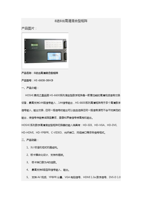
8进8出高清混合型矩阵产品图片:产品名称:8进出高清混合型矩阵产品型号:HS-6608-08HD一、产品介绍:HOSHI昊视之星品牌HS-6600系列混合型数字矩阵是一款高性能的高清视频信号交换设备,最高支持144路信号输入,144信号输出,HS-6600系列高清矩阵用于多个高清数字信号输入、输出交换,任何一路信号的输出可以自由选择任何一路信号源而不会干扰其他的输出,使信号传输衰减降至最低,图像和声音信号棱高抱枕输出。
HOSHI系列数字高清混合型矩阵切换器的输入端具有:HD-SDI、HD-VGA、HD-DVI、HD-HDMI、HD-YPBPR、C-VIDEO、光纤接口、网络接口等多种信号格式。
二、产品功能:1、3U标准机柜式机箱结构。
2、板卡模块化设计、支持热插拔。
3、板卡端口数为4的倍数。
4、最高支持8路各种信号输入、输出。
5、支持AV视频、YPBPR分量、VGA电脑信号、HDMI 1.3a数字信号、DVI-D 1.0数字信号、3G SDI 数字信号、1芯光纤信号(单多模合用)、2芯光纤信号(单多模合用)、4芯光纤信号(单多模合用)、HD Bast等信号输入。
6、支持AV视频、YPBPR分量、VGA电脑信号、HDMI 1.3a数字信号、DVI-D 1.0数字信号、3G SDI 数字信号、1芯光纤信号(单多模合用)、2芯光纤信号(单多模合用)、4芯光纤信号(单多模合用)、HD Bast等信号输输出。
7、支持FULL EDID模式,无需任何操作,插上即用。
8、Optic部分支持单模、多模光纤合用。
9、输入端、输出端内置ESD静电保护电路,即时保护设备不受外界环境干扰。
10、输入端、输出端内置EQ(信号放大)功能,无需外加信号放大器,高清信号有效传输20米、使用特定线材有效传输30米。
11、支持使用特定输出板卡HDMI-M 、DVI-M,实现无缝交换。
(可选)12、支持使用特定输出板卡HDMI-M 、DVI-M,实现信号格式转换、行频转换、场频转换、解决各种复杂的应用环境。
HDMI8808矩阵说明书V10

2 SWT 3 END
(2)、AND键:即与操作,在LCD上显示'&'字符,当一个输入 端口同时切换到 多个输出端口时,使用这个命令可以快速实现切换操作。 命令格式:输入端 口号 S WT 输出端口号 A ND 输出端口 号…AND 输出端 口 号 END 举例说明:第二路输入端口切换到第三路、第四路和第八路输出端口,应 执行以下按键操作:
图 3 搜索 2000 操作 如果此 时H D M 88 08主机已 接通电 源并且L A N网线已 连接好,将会搜索到当前局域 网内 所有的C2 0 0 0网络 设备,选 择一个 未被系统 使用的 串口,如 图4所 示:
T568B 接线顺序
引脚序号 1 2 3 4 5 6 7 8
网线颜色 橙白 橙 绿白 蓝 蓝白 绿 棕白 棕
6.2 L A N通信软件安装及使用
-7-
HDMI矩阵(HDM-8808)使用说明书 在使用L AN接口前,先安装C 2 0 0 0软件包(这个软件可 向我可以申请),安装过程采
用默 认方式即可。安 装完成后 ,在开 始菜单可 以找到如下安装 好的程序,如图2所示 。
-4-
HDMI矩阵(HDM-8808使用说明书
STO 3
( 5)、R C L键: 全称R ecal l即调用键,可以将保 存在F 0~F 9存储区中对应关系直接 调 用出来使用,省去重新设置的麻烦。 命令格式:RCL存储区(F0~F 9 ) 举例说明:调用存储 区F3的 路由 关系 ,应执行 以下按 键操作:
3.2 H D M I矩阵背面
序号 1 2 3 4 5 6 7
32进32出高清混合矩阵

32进32出高清混合矩阵 HS-6632-32HD一、产品介绍:HOSHI品牌HS-6600系列高清混合矩阵/混合高清矩阵是一款高性能的高清数字信号、模拟信号交换设备。
设备具有远程升级、远程控制、远程操作、wifi 无线控制等网络控制端口,也具有现场USB升级端口和RS232控制端口,独特的内置RTC时钟控制电路,用户可根据自身需求设定设备运行时间列表,实现无人值守。
HOSHI品牌HS-6600系列高清混合矩阵/混合高清矩阵,HS-6632-32HD规格支持32*32数字矩阵、32*32模拟矩阵、32*32数字模拟混合矩阵、32*32高清混合矩阵、32*32混合高清矩阵。
最高支持矩阵8块输入输出板卡(4路矩阵输入输出板卡/块)。
矩阵输入输出板卡任意组合、任意交换、HOSHI品牌HS-6600系列高清混合矩阵/混合高清矩阵带有断电保护、过流过压电路保护功能,所有板卡都采用支持热插拔插卡式结构设计,便于现场客户应用安装、功能升级和产品维护。
目前此机箱支持VGA视频(AV视频、CVBS视频、YPBPR分量、VGA电脑)、DVI、HDMI、3G/HD/SD-SDI、HD-Bast60米、HD-Bast100米、单芯光纤(OPTICAL)、两芯光纤(OPTICAL)、四芯光纤(OPTICAL)等信号输入输出。
HOSHI品牌HS-6600系列高清混合矩阵/混合高清矩阵用于多个高清数字信号输入输出交换、多个模拟信号输入输出交换,任何一路输入输出信号源不会干扰其他路数的输入输出信号源。
产品外观简洁化的设计,超大的OSD液晶屏幕显示(可选)、不锈钢无指纹按键(可选)、7寸液晶显示触摸屏(可选)、直观式电源管理装置(组数可选)让用户随时掌握设备的运行状态。
二、产品功能:◆9U标准机柜式机箱结构。
◆最高支持分辨率1920*1200.◆板卡模块化设计、支持热插拔。
◆板卡端口数为4的倍数。
◆最高支持32路各种信号输入、输出。
高清矩阵说明书

智能数字会议系统此次承蒙您选购高清混插矩阵系统,谨致谢意。
为了使您有正确的使用方法,请务必详读此操作说明书,并长期使用我们的产品。
敬读者尊敬的顾客,承蒙您使用我们的产品,我们谨致以衷心的感谢,产品从设计到最后的检查,中间每一步骤的质量检定都非常严谨精确,因此,我们有极大的信心保证我们的新产品能使您称心满意,在使用本产品前,请您先阅读随新产品附送的安装使用说明书,以掌握正确的使用要求。
阅读后请将本使用说明书妥善保管,以备以后操作本产品遇到问题时阅。
重要的安全事项及注意点A C100V240V~,50/60 H z1、本机可用于-。
2、为了减少火灾和触电的危险性,请不要将本机遭受雨淋或潮湿。
3、不要将线路检测器放置于直射的阳光下或靠近热源的地方。
4、不要拆除线路检测器的外壳,触摸机壳内的部件可能会导致触电和损坏线路检测器,如需进行机内维修和调整,请与指定的经销商联系。
5、线路检测器内部元件被非正式的触及,可能发生严重电击事故和损坏线路检测器,对此本公司概不负责。
6、当发现异常气味或烟雾时,请立即切断电源并拔下插头,停止使用并请专业人员检修。
7、线路检测器内部自带微处理器,切勿快速切换开关机。
8、如有任何问题,请尽快与经销商联系。
概述TS-9208H/9216H/9232H/9272H混合矩阵切换器是一款配置灵活的矩阵信号切换器。
采用高性能的硬件设计,完美支持各类高清晰数字/模拟信号切换处理,并支持双向RS-232、双向IR信号分配切换功能。
为各行业的多种视频及控制信号分配切换处理提供一站式解决方案,可广泛应用于广播电视工程、多媒体会议厅、大屏幕显示工程、电视教学、指挥控制中心等场所。
TS-9208H/9216H/9232H/9272H混合矩阵切换器提供HDMI、DVI、VGA、CVBS、S-Video、YPbPr信号本地直连输入,以及HDMI、DVI直连输出。
除此之外,还提供双绞线(HDBaseT)输入输出板卡,配合双绞线传输器可通过双绞线延长输入与输出的信号传输距离到100M,另外还提供光纤输入输出板卡,配合光纤传输器通过单芯多模光纤延长输入与输出的信号传输距离到300M,更可更换为使用单模光纤传输的单模收发器提升传输距离达20KM。
S-mix无缝切换矩阵说明书

为确保设备可靠,使用及人员的安全,在安装、使用和维护时,请遵守以下事项:
请注意机箱接地良好
设备通电前,需要检查确保机箱接地良好,以防止机壳产生静电放电而危及设备和 人身安全,并起到良好的屏蔽效果。
� � �
不要将系统设备置于过冷或过热的地方。 设备电源在工作时会发热, 因此要保持工作环境的良好通风, 以免温度过高而损坏设备。 阴雨潮湿天气或长时间不使用时,应关闭电源总闸。 非专业人士未经许可,请不要试图拆开设备机箱,不要私自维修,以免发生意外 事故或加重设备的损坏程度。
图三 切换界面---输入端口
图四 切换界面---输出端口
如按照图三和图四的操作,可以实现将输入通道 1 切换到输出通道 1,2,11,12,18。
5.4 通讯端口定义
矩阵提供标准串行通讯端口、LAN 网络控制口,除了可以利用液晶触控方式进行切 换操作外,还允许用户使用各种控制系统(如个人电脑、其他控制系统)进行控制或通过以 太网进行远程控制。可用串口直连线与电脑串口连接,安装好应用软件后,即可利用电脑对 矩阵进行控制。 用户可使用矩阵附带的应用软件作为电脑控制软件, 也可以自行编写控制软 件,详情可参考“矩阵RS232 通讯协议及控制代码” 。S-Mix和电脑连接时需要使用交叉性 RS232线缆。
�
不要将任何化学品或液体洒在设备上或其附近。
一、 二、 三、 四、 五、 5.1 5.2 5.3 5.4 5.5
产品简介...........................................................................................................................3 产品指标...........................................................................................................................3 规格指标...........................................................................................................................4 标配清单...........................................................................................................................4 设备操作及功能说明.......................................................................................................5 设备操作.......................................................................................................................5 混合矩阵切换系统应用............................................................................................... 5 S-MIX 矩阵切换说明...................................................................................................6 通讯端口定义............................................................................................................... 8 矩阵 PC 软件使用方法............................................................................................... 8 A. B. 串口 RS232 控制矩阵操作步骤............................................................................. 9 LAN 口控制矩阵操作步骤....................................................................................12
HWT-DEC808网络矩阵8通道HDMI输出说明书

HWT-DEC808Network Matrixwith 8ch HDMI outputFeaturesSpecificationsModel work Matrix with 8ch HDMI output Module or Interface Input none Output 8ch HDMI output Ethernet 100M/1000M self adaptive Audio input 4ch ,by Ф3.5 audio interface Audio output 4ch ,by Ф3.5 audio interface Alarm output support network alarm input USB2.0support RS232/422/485support VideoNetwork videodecodingH.265,H.264Network videoinput4K, 1080P,1080I,720P,D1HDMI ouput resolution 1024×768P@60hz,1280×720P@60hz,1366×768P@60hz,1920×1080P@60hz,3840×2160@60hz Video decodeand display8ch 4K or 64ch 1080P or 128ch 720P or 256ch D1Monitor splicing 8 monitor to splice and display one videoSplitmaximum 64 split,1/4/6/8/9/10/16/25/36/64 splittingmode and display ,or split by user-define.OSD Window, Channel,label, alarm, etc. information AudioAudio Codec G.711,G.726,ADPCM encode/decode On/Mute Supports all channels and single channel set individually Audio input 4ch audio encode, it can open/close audio input.Management and MaintenanceBasic applications maximum 72users online at same timeusers permission definition ;video switch and control Cruise, patrol, split,etc.display mode management, Planconfiguration and call.Management &ConfigurationPETNET protocol available, third party Net client orplatform can configure and manage this matrix on usersoperation permission definition & managementMaintenancesystem log , System status detection,Fault detection andreport, support online updatingInitialization set it can configure accordingly.Othertimesynchronization interior RTC, it could time automatic sync.in cascading .PENET or standard port, to keep sync. to time serverinside the system.Alarm network alarm input, alarm action to call video display Alarm process manual or automatic Power supply AC100 to 230Consumption ≤96W Working temp.0~45℃Workinghumidity 10%~90%Weight Gross/net weight: 6.5kgs/4.5kgsDimensioncarton size: 580.0mm(L)×540.0mm(W)×160.0mm(H)product size:482.0mm(L)×371.3mm(W)×44.0mm(H)In generalHWT-DEC808 Network matrix is with 8ch hdmi output,can decode stream of onvif/H265/264 & RTSP, etc.from ip camera or platform, restore HD signal and display on monitors, perfect video wall management, including split, splicing, PIP, Plan, Cruise, etc.simple operation likeanalog system.Besides it offers audio codec, alarm action, etc. functions for multiple applications.Dimension◼Support network media input ;◼Support multiple resolution of output, it can manually set output resolution ;◼Output supports maximum 3840x2160@60Hz ;◼Support 4K,1080P ,1080I,720P ,D1video formats ;◼H265/H264compatible ;◼Support 8ch 4K or 64ch 1080P or 128ch 720P decoding and display ;◼Support video-splitting output,up to 64windows split on one monitor ;◼Support Cruise,Plan,split,splicing,etc.display mode ;◼Support Plan configuration and management ;◼Optimize video ,it can make video stream smooth andimprove network jammed . ◼Support intelligent connection ;◼Support audio input and output◼Support alarm linkage action and contact closure output ;◼Support OSD, title, time and warning messages canoverlap on the displayed video ;◼Support multiple label program, can configure labelposition freely;。
DS-HX7308BTJFA%20Datasheet--Ver04[1]
![DS-HX7308BTJFA%20Datasheet--Ver04[1]](https://img.taocdn.com/s3/m/ebe48281680203d8ce2f240e.png)
Himax Display, Inc.( DOC No. HX7308BTJFA-DS )HX7308BTJFA1024X768 0.45” LCOS ModuleVersion 04 February, 2011DA T A SHEET2 0 1 1 . 0 2 .D C Ce ‡ö{¡R 6Himax 立景光電股份有限公司 文 件 發 行 及 參 考 文 件 TO :中科院半导体研究所 Date :2011/02/24DOCUMENT CONTROL CENTERHimax Display, Inc.Revision HistoryVersion Date Author Description of Changes012009/12Linda LeeNew setup02 2010/04Linda Lee Angela Lu1. Modified Figure10.7 R-V Curves Y-V Curves2. Revised Table 9.1:add ESD data3. Revised Table 9.2:add Operation frequency data(Max.:64MHz)4. Revised Table 9.45. Revised section 8.96. Revised Table 10.2 Optical specification(CR:300 350,Wx:0.318 0.34,Wy:0.345 0.37) 7. Revised Figure14.1 Mechanicaldrawing(Shift:X/Y:+/-0.3mm +/-0.15mm)8. Revised Table10.2:Response time Effective LC response time9. Modified Table10.2(Note4): Definition of effective LC response time T eff 10. M odified Table 8.203 2010/08 Linda Lee1. Update Table8.1 Horizontal Total:138(Min) 148(Min)04 2011/02 Linda Lee1. Update Figure10.5 Panel reflection spectrum and Figure10.6 YV curves2. Revised Reliability specificationHTHHST: 85 ºC,85%RH,120 hrs-->60ºC,90%RH,240 hrs 3. Revised Table 4.1 Note2 description 4. Modified section 8.2 and 9.2 data 5. Revised section 8.9 and 9.3 formatHX7308BTJFA1024X768 0.45” LCOS ModuleVersion 04February, 20112 0 1 1 . 0 2D C Ce‡NContents1.About This Document (4)2.General Description (4)3.Features (4)4.Quick Reference Data (5)5.Block Diagram (6)6.Pin Assignment (6)7.Pin Description (7)8.Function Description (8)8.1Embedded Timing Controller (8)8.2Input Timing (8)8.3Relationship between Input Data and Output Position (9)8.4Relationship between Input Data and Output Voltage (10)8.5Gamma Correction Characteristic Curve (10)8.6Programmable Gamma Buffer (11)8.7Serial Interface (11)8.8Details of Read/Write Sequence Through Two-Wired Serial Interface (12)8.9I2C Description (13)9.Electrical Characteristics (15)9.1Absolute Maximum Ratings (15)9.2Recommended Operating Conditions (15)9.3DC Electrical Characteristics (16)9.3.1DC Characteristics (16)9.3.2Power Consumption (16)9.4AC Electrical Characteristics (17)10.Optical Characteristics (18)10.1Test Conditions (18)10.2Optical Specifications (18)10.3HX7308 Panel Reflection Spectrum (22)10.4HX7308 Panel Y-V Curves (22)11.Reliability Specification (23)12.Package Specifications (24)12.1Packing Procedure (24)12.2Label Information13.Green Product14.Mechanical DimensionFigure 5.1 Block Diagram (6)Figure 8.1 Display Result (9)Figure 8.2 Timing diagram of CLK, input data, and start pulse input/output (this is LR=H) (9)Figure 8.3 Positive Polarity (10)Figure 8.4 Negative Polarity (10)Figure 8.5 Read/Write Sequence of the Two-Wired Serial Bus (12)Figure 8.6 Timing Diagrams of SCL and SDA (12)Figure 9.1 Input Timing Diagram (17)Figure 10.1 MDIS Optic Measurement Systems (19)Figure 10.2 Polarization Direction of Entrance (19)Figure 10.3 Definition of ANSI 9 Points on Panel (20)Figure 10.4 Definition of T eff (21)Figure 10.5 Panel Reflection Spectrum (22)Figure 10.6 HX7308 Y-V Curve (22)Figure 12.1 Packing Procedure (24)Figure 12.2 Label Information (25)Figure 12.3 Green Product Label (25)Figure 14.1 Mechanical Dimension (26)List of TablesTable 4.1 Reference Data (5)Table 7.1 Pin Description (7)Table 8.1 Timing Parameter (8)Table 8.2 Relationship between Input Data and Output Position (9)Table 8.3 I2C Registers for Standard Settings (13)Table 8.4 Description of Control Setting (13)Table 8.5 I2C Registers for Default Settings (13)Table 9.1 Absolute Maximum Ratings (15)Table 9.2 Recommended Operation Conditions (15)Table 9.3 DC Electrical Characteristics (16)Table 9.4 Power Consumption (16)Table 9.5 AC Electrical Characteristics (17)Table 10.1 Test Condition (18)Table 10.2 Optical Specifications (18)Table 11.1 Reliability Specification (23)This document is the HX7308BTJFA draft datasheet.Note: HX7308BTJFA is already under Mass production.2. General DescriptionHX7308BTJFA is an active matrix liquid crystal display with resolutions of 1024X768. Horizontal digital data drivers and vertical scan drivers are integrated with pixel device to meet the performance demands of high-speed and high–resolution display applications.HX7308BTJFA embedded timing controller generates internal control signals and display high-brightness and high-contrast ratio image quality by color sequential process. HX7308BTJFA received 8-bits x 4 dots of digital display data per positive clock edge and 8-bits x 4 dots of digital display data per negative clock edge from external, and generates corresponding voltage output of 256-level gray scale.HX7308BTJFA embedded Two-wired serial bus that can be used to programming gamma voltage and COM directly.3. FeaturesLCOS color sequential panel with resolution 1024X768.Support display mode: 1024 x 768 color sequential.Support display sequence: RGBRGB,RRGGBB,RRGGBBGGNo spacers in the display area.Integrated horizontal data and vertical scan drivers.Capable of displaying 256 gray scales by 8 internal gamma reference voltages.Embedded 8 channels programmable gamma reference voltages.Embedded programmable reference voltage generators are for setting LC common electrical node voltage.Embedded programmable reference voltage generators are for pixel reset and discharge all single cells.Embedded timing controller.Horizontal and vertical bi-directional scanning.Two-wired serial interface for internal register setting.Interface is 4 port dual-edge.COM modulation.Operation powers : analog power(6V), and digital power(1.8V).Module Pin number=45Ideal for mini-projector applicationTable 4.1 Reference DataDescription Specification Unit Active Area Diagonal 0.45” InchesActive Area Dimensions 9.215 X 6.915 mmNative Aspect Ratio 4:3 -Display Resolution 1024 X 768 pixelsPixel Pitch 9 X 9 um Pixel Configuration Orthogonal -Gray Level 256 ( 8-bits ) - Typical Contrast ratio @ F/2.5 350 - Typical Reflectance 66(Note 1)%Optical Mode Reflective - Liquid Crystal Mode Twist Nematic Mode -Operation Mode Normally White -Effective LC Response Time (Teff)0.2 ms Operation Temperature 0~50(Note 2)℃All values specified at a display ambient temperature of 25℃.Note 1: For light with wavelength from 430mm to 650mmNote2: Due to the characteristics of Liquid Crystal, the imager's display quality might be worse at low or high temperature.Even Source DriverDisplay Area (1024x768)Odd Source DriverGate DriverBus ControlProgrammable Gamma BufferTwo-WiredSerial BusTCONSCL/SDAVideo InputPowerPower InFigure 5.1 Block Diagram6. Pin AssignmentPin Pin Name Pin Pin Name Pin Pin Name 1 COM 16 RESETB 31 DC1 2 VDDA 17 DB0 32 DC2 3 RREF 18 DB1 33 DC3 4 VSSA 19 DB2 34 DC4 5 SDA 20 DB3 35 DC5 6 SCL 21 DB4 36 DC6 7 DA0 22 DB5 37 DC7 8 DA1 23 DB6 38 DD0 9 DA2 24 DB7 39 DD1 10 DA3 25 CLKX 40 DD2 11 DA4 26 DE 41 DD3 12 DA5 27 INV1 42 DD4 13 DA6 28 VSSD 43 DD5 14 DA7 29 INV2 44 DD6 15VDDD30DC045DD7Table 7.1 Pin DescriptionPin name Pin#Type Function DescriptionDA[7:0] DB[7:0] DC[7:0] DD[7:0]7~14,17~24,30~45InputTTL display data input. The display data is input in 8-bit × 4 dotsper positive CLKX edge, and 8-bit × 4 dots per negative CLKXedge. For each input dot, Dx0 is LSB and Dx7 is MSB.DE 26 Input Display active. CMOS input pin.CLKX 25 Input X-axis shift clock input. The display data is stored to the internal data register at the rising edge and falling edge of CLKX.INV1 27 Input INV signal for DA[7:0] & DB[7:0] to decrease EMI issue. INV2 29 Input INV signal for DC[7:0] & DD[7:0] to decrease EMI issue.SDA 5 I/O Data for Two-wired serial interface. Connect to VDDD with a pull-up resistor.SCL 6 Input Clock for Two-wired serial interface. Connect to VDDD with a pull-up resistor.COM 1 Output Reference common voltage output. Internal reference common voltage output. (No current)RREF 3 Output Bias control pin. Connect to VSSA with a bias resistor 39KΩ to generate driver bias current.RESETB 16 Input Active low reset. When RESETB=0, panel is reset. VDDA 2 Power Driver power supply. Connect to 6V power source. VDDD 15 Power Logic power supply. Connect to 1.8V power source. VSSA 4 Ground Ground for VDDAVSSD 28 Ground Ground for VDDDThis section describes about the following topic:Embedded timing ControllerInput TimingRelationship between Input Data and Output PositionRelationship between Input Data and Output VoltageGamma Correction Characteristic CurveProgrammable Gamma BufferSerial InterfaceDetails of Read/Wire Sequence Through Two-Wired Serial Interface8.1 Embedded Timing ControllerEmbedded timing controller (TCON) is controlled by Two-wired serial interface for programming internal register file. The addressing of register mapping file is shown Table 8.3I2C Register Table.8.2 Input TimingXGA:Table 8.1 Timing ParameterDescription Min. Typ. Max. UnitHorizontal Total 148 168 189 8 PixelHorizontal Display - 128 - 8 PixelHorizontal Blanking - 40 - 8 PixelVertical Total 792 806 2160 LineVertical Display - 768 - LineVertical Blanking - 38 - LineFrame Rate - 360 - HzPixel Clock - 48.75 64 MHzData Rate - 97.5 128 Mbps8.3 Relationship between Input Data and Output PositionTable 8.2 Relationship between Input Data and Output PositionInput data format:8-bit × 4 (4 pixels per CLK)Input data width: 32bits (4 pixels data) with X7 is MSB and X0 is LSBData first→ Data lastLR DA [7:0] DB [7:0] DC [7:0] DD [7:0] ••• DA [7:0] DB [7:0] DC [7:0] DD [7:0] “H” OUT1/ OUT2/ OUT3/ OUT4••• OUT1021/ OUT1022/ OUT1023/OUT1024Data last← Data firstLR DD [7:0] DC [7:0] DB [7:0] DA [7:0] ••• DD [7:0] DC [7:0] DB [7:0] DA [7:0] “L” OUT1/ OUT2/ OUT3/ OUT4••• OUT1021/ OUT1022/ OUT1023/OUT1024UD Scan first → Scan last “H” Line 1 ••• Line 768 UD Scan last ← Scan first “L” Line 1•••Line 768Figure 8.1 Display ResultCLKXDD[7:0]Out4Out8Out12Out16Out1024Out1020Out1016Out1012DC[7:0]Out3Out7Out11Out15Out1023Out1019Out1015Out1011DB[7:0]Out2Out6Out10Out14Out1022Out1018Out1014Out1010DA[7:0]Out1Out5Out9Out13Out1021Out1017Out1013Out10098.4 Relationship between Input Data and Output VoltageThe output voltage is determined by the 8-bit digital input data, positive polarity, negative polarity, Gamma correction reference voltage inputs. V gma1p ~ V gma8p are for positive polarity gamma voltage output. V gma1n ~ V gma8n are for negative polarity gamma voltage output.8.5 Gamma Correction Characteristic CurveFigure 8.3 Positive PolarityFigure 8.4 Negative PolarityCOMNV gma8nV gma7nV gma6nV gma5nV gma4n V gma3nV gma2nV gma1n0 40 76 112 148 184 220 255Input dataCOMP V gma8pV gma7pV gma6pV gma5p V gma4p V gma3p V gma2pV gma1p0 40 76 112148 184 220 255 VDDAVSSAVDDAVSSA8.6 Programmable Gamma BufferHX7308BTJFA contains 16 programmable Gamma buffers. Each contains rail-to-rail output buffer and 8 bit resolution DAC (Digital to Analog Converter) with resistor-string voltage reference input. Reference voltage level is written by Two-wired serial interface. Detail programmable address and default value refer to Table 8.3 Since the input coding to the DAC is straight binary and functions of positive polarity, negative polarity, gamma voltage and COM, the ideal output voltage is given by:D VDDAVDDA V out ×−=255Where D = decimal equivalent (0~255) of the binary code that is loaded to the DAC register.8.7 Serial InterfaceHX7308BTJFA is controlled via a Two-wired serial interface. The device isconnected to this bus as slave devices. HX7308BTJFA has a 7-bit slave address. Seven MSBs are 1001001.The Two-wired serial bus protocol operates as follows: 1. The master initiates data transfer by establishing a START condition, when ahigh-to-low transition on the SDA line occurs while SCL is high. The following byte is the address byte, which consist 7-bit slave address followed by an R/W bit (this bit determines whether data will be read from or written to the slave device).The slave’s address corresponds to the transmitted address responds by pulling SDA low during the 9th clock pulse (this is termed the Acknowledge bit). At this stage, all other devices on the bus remain idle while the selected device waits for data to be written to or read from its shift register.2. Data is transmitted over the serial bus in sequences of nine clock pulses (eightdata bits followed by an Acknowledge bit). The transitions on the SDA line must occur during the low period of SCL and remain stable during the high period of SCL.3. When all data bits have been read or written to, a STOP condition isestablished. In Write/Read mode, the master will pull the SDA line high during the 10th clock pulse to establish a STOP condition. The master will then bring the SDA line low before the 10th clock pulse and then high during the 10th clock pulse to establish a STOP condition.DATA SHEET V048.8 Details of Read/Write Sequence Through Two-Wired Serial InterfaceS1001001W APS111W S 1001001R A PAA AA A S1001001W AAAAA PS1001001W S 1001001R AA AA PA7 b it a d d re s s7 b it a d d re ss7 b it a d d re s sS T A R T c o n d itio nre g is te r a d d re ss re g is te r d a taA ck n o w le d g eA c k n o w le d g eT O P c o n d itio n re g is te r a d d re ssre g is te r d a tare g is te r d a taA c k n o w le d g e S T A R T c o n d itio nW R IT E co m m a n dD ire c tio n :F ro m m a s te r to d e vic eF ro m d e v ic e to m a s te rN o te : R =R E A D =1 a n d W = W rite =0Figure 8.5 Read/Write Sequence of the Two-Wired Serial BusFigure 8.6 Timing Diagrams of SCL and SDA1DATA SHEET V04 8.9 I2C DescriptionTable 8.3 I2C Registers for Standard SettingsADDR.A7 A6 A5 A4 A3 A2 A1 A0 Suggest Value note[ 00 ]h LR UD INV12_EN 1 0 SC_I2C 1 0 [ 1111 0010 ] control setting[ 01 ]h0 1 0 0 0 1 1 1 [ 0100 1111 ] standard setting [ 47 ]h0 TRIGMA 1 1 1 1 0 0 [ 0111 1111 ] standard setting [ 0c ]h0 0 0 0 0 0 0 0 [ 0001 0100 ] COMN[ 0d ]h 1 1 1 1 1 1 1 1 [ 1110 1001 ] COMPTable 8.4 Description of Control SettingRegister Setting Description0, Display right to leftLR1, Display left to right (Default)0, Display down to upUD1, Display up to down (Default)0, Disable INV functionINV12_EN1, Enable INV function (Default)0, Disable single cell (Default)SC_I2C1, Enable single cell0, All refer to R gamma (Default)TRIGMA1, Enable R/G/B gamma select functionTable 8.5 I2C Registers for Default SettingsADDR.A7 A6 A5 A4 A3 A2 A1 A0 note[ 10 ]h0 0 0 0 0 0 0 0 GMAR1P[ 11 ]h0 0 0 0 0 0 0 0 GMAG1P[ 12 ]h0 0 0 0 0 0 0 0 GMAB1P[ 13 ]h 1 1 1 1 1 1 1 1 GMAR1N[ 14 ]h 1 1 1 1 1 1 1 1 GMAG1N[ 15 ]h 1 1 1 1 1 1 1 1 GMAB1N[ 16 ]h0 1 1 0 1 0 0 0 GMAR2P[ 17 ]h0 1 1 0 1 0 0 0 GMAG2P[ 18 ]h0 1 1 0 1 0 0 0 GMAB2P[ 19 ]h 1 0 0 1 0 1 1 1 GMAR2N[ 1a ]h 1 0 0 1 0 1 1 1 GMAG2N[ 1b ]h 1 0 0 1 0 1 1 1 GMAB2N[ 1c ]h0 1 1 1 1 1 1 1 GMAR3P[ 1d ]h0 1 1 1 1 1 1 1 GMAG3P[ 1e ]h0 1 1 1 1 1 1 1 GMAB3P[ 1f ]h 1 0 0 0 0 0 0 0 GMAR3N[ 20 ]h 1 0 0 0 0 0 0 0 GMAG3N[ 21 ]h 1 0 0 0 0 0 0 0 GMAB3N[ 22 ]h 1 0 0 1 0 1 0 0 GMAR4P[ 23 ]h 1 0 0 1 0 1 0 0 GMAG4P[ 24 ]h 1 0 0 1 0 1 0 0 GMAB4P[ 25 ]h0 1 1 0 1 0 1 1 GMAR4N[ 26 ]h0 1 1 0 1 0 1 1 GMAG4N[ 27 ]h0 1 1 0 1 0 1 1 GMAB4N[ 28 ]h 1 0 1 0 1 0 1 0 GMAR5P [ 29 ]h 1 0 1 0 1 0 1 0 GMAG5P [ 2a ]h 1 0 1 0 1 0 1 0 GMAB5P [ 2b ]h0 1 0 1 0 1 0 1 GMAR5N [ 2c ]h0 1 0 1 0 1 0 1 GMAG5N [ 2d ]h0 1 0 1 0 1 0 1 GMAB5N [ 2e ]h 1 0 1 1 1 1 1 1 GMAR6P [ 2f ]h 1 0 1 1 1 1 1 1 GMAG6P [ 30 ]h 1 0 1 1 1 1 1 1 GMAB6P [ 31 ]h0 1 0 0 0 0 0 0 GMAR6N [ 32 ]h0 1 0 0 0 0 0 0 GMAG6N [ 33 ]h0 1 0 0 0 0 0 0 GMAB6N [ 34 ]h 1 1 0 1 0 1 0 1 GMAR7P [ 35 ]h 1 1 0 1 0 1 0 1 GMAG7P [ 36 ]h 1 1 0 1 0 1 0 1 GMAB7P [ 37 ]h0 0 1 0 1 0 1 0 GMAR7N [ 38]h0 0 1 0 1 0 1 0 GMAG7N [ 39]h0 0 1 0 1 0 1 0 GMAB7N [ 3a ]h 1 1 1 1 1 1 1 1 GMAR8P [ 3b ]h 1 1 1 1 1 1 1 1 GMAG8P [ 3c ]h 1 1 1 1 1 1 1 1 GMAB8P [ 3d ]h0 0 0 0 0 0 0 0 GMAR8N [ 3e ]h0 0 0 0 0 0 0 0 GMAG8N [ 3f ]h0 0 0 0 0 0 0 0 GMAB8N [ 40 ]h 1 1 1 1 1 1 1 1 RINGP [ 41 ]h0 0 0 0 0 0 0 0 RINGN9. Electrical CharacteristicsThis section describes about the following topic: Absolute Maximum Ratings Recommended Operating Conditions DC Electrical Characteristics AC Electrical Characteristics9.1 Absolute Maximum RatingsTable 9.1 Absolute Maximum RatingsParameter Symbol Rating Unit VDDA -0.5 to +6.8 V Power supply voltage VDDD -0.5 to +2.3 V Input voltageCMOS/TTL Input-0.5 to +2.3 V HBM±2000 V MM ±200 V CDM ±1000 V ESDLatch-up±100mANote: The device is subject to be damaged permanently if stresses beyond thoseabsolute maximum ratings listed above.9.2 Recommended Operating ConditionsTable 9.2 Recommended Operation ConditionsRating Parameter Symbol Min. Typ. Max. Unit VDDA 5.8 6.0 6.6 V Power supply voltage VDDD 1.65 1.8 1.95 V Vgma1n ~ Vgma8n 0.2 - 5.8 V Gamma correction reference voltage @VDDA=6.0V Vgma1p ~ Vgma8p0.2 - 5.8 V Operation frequency f CLKX - 48.75 64 MHz Operation data rateDR-97.5128Mbps9.3.1 DC CharacteristicsTable 9.3 DC Electrical CharacteristicsSpecification Parameter Symbol ConditionMin. Typ. Max.UnitHigh level inputvoltageVIH1 0.7×VDDD- VDDDLow level input voltage VIL1DA[7:0], DB[7:0],DC[7:0], DD[7:0],CLKX, DE, RESETB0 - 0.3×VDDDVHigh level inputvoltageVIH2 0.8×VDDD- VDDDLow level input voltage VIL2SDA, SCL0 - 0.2×VDDDVInput leakagecurrentIIH/IIL Digital Input Pins -1 - 1 µAStatic current I VDDD_STA VDDD=1.8VRESET=0- 1 - uANote:All values specified at a display ambient temperature of 25℃.9.3.2 Power ConsumptionTable 9.4 Power ConsumptionSpecification Parameter Symbol ConditionMin. Typ. Max.UnitPattern=256-Gray f CLKX=48.75MHz - 6 - mACurrent of VDDAI VDDA_ACT@VDDA=6.0V Patte rn=1 Pixel On/Offf CLKX=64MHz- 10 - mAPattern=256-Grayf CLKX=48.75MHz- 11 - mA Current of VDDDI VDDD_ACT@VDDD=1.8V Pattern=8 Pixel On/Offf CLKX=64MHz- 18 - mATable 9.5 AC Electrical CharacteristicsSpecification Parameter Symbol Min. Typ. Max. Unit Clock pulse width t CLKX 15.6 20.50 - ns Clock pulse low period t CLKX(L) 7.8 10.25 - ns Clock pulse high period t CLKX(H) 7.8 10.25 - ns Data setup time1 t SETUP1 1 - - ns Data hold time1 t HOLD1 2 - - ns Data setup time2 t SETUP2 1 - - ns Data hold time2t HOLD22--nsCLKXt CLKXt CLKX(H)t CLKX(L)t SETUP1t HOLD1t SETUP2t HOLD2DD[7:0]Out4Out8Out12Out16Out1024Out1020Out1016Out1012DC[7:0]Out3Out7Out11Out15Out1023Out1019Out1015Out1011DB[7:0]Out2Out6Out10Out14Out1022Out1018Out1014Out1010DA[7:0]Out1Out5Out9Out13Out1021Out1017Out1013Out1009Figure 9.1 Input Timing Diagram10. Optical CharacteristicsReflective twisted-nematic liquid crystal mode is employed in HX7308BTJFA.When no voltage is applied, HX7308BTJFA presents bright state (i.e. the normally white mode). The images darken up as the applied voltage increases. Different gray-level can be obtained by tuning the applied voltage. HX7308BTJFA is a color sequential LCOS display that exhibits color images by single panel.10.1 Test ConditionsTable 10.1 Test ConditionItemSymbol Value UnitAmbient Temperature Ta 25±5℃ Ambient Humidity Ha 50±20%RH Supply Voltage VDDA6.0 VInput SignalAccording to typical value in “ELECTRICAL CHARACTERISTICS”10.2 Optical SpecificationsTable 10.2 Optical SpecificationsItemConditionMin. Typical Max. UnitNotesReflectance %(430~650nm) @F/2.5 58 66 - % Note (1) Uniformity of Reflectance Measure 9 points asfigure 10.3 80 90 - % Note (2) Contrast Ratio Full white/black @F/2.5200 350 - - Note (3)x 0.30 0.34 0.38 - White Balancey%(430~650nm)@F/2.5 0.33 0.37 0.41 - Effective LCResponse TimeT eff Transition from 90%10% @ 50 deg.C-0.2-msNote (4)PS. All values are measured the normal direction to the panel.Note (1) Definition of Reflectance and white coordinates : Reflectance and white coordinates are measured by MDIS (Westar Inc.) Measure the Reflectance and white coordinates of gray scale 255 at center point. Figure 10.1 shows the optic measurement system of MDIS. Figure 10.2 shows the polarization direction of entrance light.Figure 10.1 MDIS Optic Measurement SystemsFigure 10.2 Polarization Direction of EntranceEntrance LightPolarization DirectionDATA SHEET V04 Note (2) Definition of Uniformity of ReflectanceMeasure the luminance of gray 255 at 9 points by MDIS.Uniformity = Minimum[L(1),L(2),L(3),L(4),L(5),L(6),L(7),L(8),L(9)] /Maximum[L(1),L(2),L(3),L(4),L(5),L(6),L(7),L(8),L(9)]Figure 10.3 Definition of ANSI 9 Points on PanelNote (3) Definition of Contrast Ratio:Luminance of gray 255 and gray 0 was measured by MDIS at the center point.The contrast ratio can be calculated by the following expression.CR=L255/L0PS: 1. L255 = Luminance of gray level 2552. L0 = Luminance of gray level 0DATA SHEET V04Note (4) Definition of effective LC response time T effMeasured by HIMAX DISPLAY photo diode sensor & oscilloscope under temperature 50℃.Figure 10.4 Definition of T effThe effective LC response time, T eff , is defined as the response time of LC at the color interchange period. It is the response time that influences the color gamut and the maximum LED duty.Ex: When showing red image, the slow T eff will cause green light leakage as in the oblique line area. Therefore, it will contaminate the purity of the red image.LC response curveR LED IlluminationG LED IlluminationG light leakage90%10%TimeT effIntensityHX7308BTJFA 1024X768 0.45” LCOS ModuleDATA SHEET V0410.3HX7308 Panel Reflection SpectrumReflection spectrum is measured by MDIS (Westar Inc.)White Spectral Response01020304050607080400440480520560600640680720Wavelength (nm)R e f l e c t a n c e (%)Figure 10.5 Panel Reflection Spectrum10.4 HX7308 Panel Y-V CurvesThe Y-V Curve is measured by MDIS (Westar Inc.).0%10%20%30%40%50%60%70%80%90%100%0123456Voltage(volt.)N o r m a l i z e d Y (%)Figure 10.6 HX7308 Y-V CurveY (CIE1931) can be calculated by panel reflectance as shown below.whereR is the reflectance of the panel λ is the wavelength and k is a constant :is a color matching functionNormalized Y = Y/Ymax∫×=nm nm d y R k Y 650430)()(λλλλλd y k nmnm∫=650430)(100y 2 0 1 1 . 0 2 H i x D i yD C Ce ‡ö{¡R 6HX7308BTJFA1024X768 0.45” LCOS ModuleDATA SHEET V0411. Reliability SpecificationTable 11.1 Reliability SpecificationItemSpecification Judgment CriteriaHTST :High Temperature Storage Test95 ºC , 240 hrsLTST :Low Temperature Storage Test-40ºC , 240 hrsHTHHST :High Temperature and High Humidity Storage Test60 ºC , 90%RH , 240 hrs TS : Thermal Shock Test -40 ºC (1 hr ) / 85ºC (1 hr ), 30 cycles HTOP :High Temperature Operation Test 70 ºC , 240 hrsHTHHOP High Temperature and High Humidity Operation Test 50 ºC, 90%RH , 240 hrs LTOP :Low Temperature Operation Test-20 ºC, 240 hrs ALT Altitude Test193mbar(12,000m) ,72 hrsAfter being returned tothe normal temperatureand being left for morethan 2 hours , the judgment is made according to Note A 、B 、C 、DCNTPIOConnector Plug In and Out20 timesFPCBFPC Bending Test ± 90 degree, 10 times Package Vibration Proof Follow ISTA Spec, 1 BoxPackage Drop TestFollow ISTA Spec, 1 BoxAfter test , the judgment is made according to Note B 、C 、DNote:A. CR after RA test is higher than one half of the initial CR.B. No functional failure.C. No extra mura or defect.D. No obvious deformation or break.2 0 1 1 . 0 2 H i m a x D i s pD C Ce‡N öHX7308BTJFA1024X768 0.45” LCOS ModuleDATA SHEET V0412. Package Specifications․ Box content :12 trays + cover tray. (Note: Each tray can contain 20 panels). ․ Box dimension :368 (L) x 175 (W) x 245 (H) (Unit : mm) ․ Gross Weight :Approximately 1.5 kg12.1 Packing ProcedureFigure 12.1 Packing Procedure12trays + cover 20panels per traySpongeCartonGreen product labelGreen product labelPlasticsCarton label2 0 1 1 . 0 2 . 2 H i m a x D i s p D C Ce‡N ö{R 612.2 Label Information12.2.1 Carton labelLabel information indicate grading of LCOS module, part ID, module name and shipping quantity.14. Mechanical DimensionThe mechanical dimensions are for customer’s reference design-in purpose. The mechanical dimensions has indicated as the drawing number, 7308FA5600AA00 as shown on the following page.Figure 14.1 Mechanical Dimension。
- 1、下载文档前请自行甄别文档内容的完整性,平台不提供额外的编辑、内容补充、找答案等附加服务。
- 2、"仅部分预览"的文档,不可在线预览部分如存在完整性等问题,可反馈申请退款(可完整预览的文档不适用该条件!)。
- 3、如文档侵犯您的权益,请联系客服反馈,我们会尽快为您处理(人工客服工作时间:9:00-18:30)。
无缝高清混合矩阵 HS-6608M-08HD
一、产品介绍:
HOSHI品牌HS-6600M系列无缝高清混合矩阵/无缝混合高清矩阵是一款高性能的高清数字信号、模拟信号交换设备。
设备具有远程升级、远程控制、远程操作、wifi无线控制等网络控制端口,也具有现场USB升级端口和RS232控制端口,独特的内置RTC时钟控制电路,用户可根据自身需求设定设备运行时间列表,实现无人值守。
HOSHI品牌HS-6600M系列无缝高清混合矩阵/无缝混合高清矩阵,
HS-6604M-04HD规格支持8*8数字矩阵、8*8模拟矩阵、8*8数字模拟混合矩阵、8*8高清混合矩阵、8*8混合高清矩阵。
最高支持矩阵2块输入输出板卡(4路矩阵输入输出板卡/块)。
矩阵输入输出板卡任意组合、任意交换、HOSHI品牌HS-6600M系列无缝高清混合矩阵/无缝混合高清矩阵带有断电保护、过流过压电路保护功能,所有板卡都采用支持热插拔插卡式结构设计,便于现场客户应用安装、功能升级和产品维护。
目前此机箱支持VGA视频(AV视频、CVBS视频、YPBPR分量、VGA电脑)、DVI、HDMI、3G/HD/SD-SDI、HD-Bast60米、HD-Bast100米、单芯光纤(OPTICAL)、两芯光纤(OPTICAL)、四芯光纤(OPTICAL)等信号输入输出。
HOSHI品牌HS-6600M系列无缝高清混合矩阵/无缝混合高清矩阵用于多个高清数字信号输入输出交换、多个模拟信号输入输出交换,任何一路输入输出信号源不会干扰其他路数的输入输出信号源。
产品外观简洁化的设计,超大的OSD
液晶屏幕显示(可选)、不锈钢无指纹按键(可选)、7寸液晶显示触摸屏(可选)、直观式电源管理装置(组数可选)让用户随时掌握设备的运行状态。
二、产品功能:
1、3U标准机柜式机箱结构。
板卡模块化设计、支持热插拔。
板卡端口数为4的倍数。
最高支持08路各种信号输入、输出。
2、支持AV视频、YPBPR分量、VGA电脑信号、HDMI 1.3a数字信号、DVI-D 1.0数字信号、3G SDI 数字信号、1芯光纤信号(单多模合用)、2芯光纤信号(单多模合用)、4芯光纤信号(单多模合用)、HD Bast等信号输入。
3、支持AV视频、YPBPR分量、VGA电脑信号、HDMI 1.3a数字信号、DVI-D 1.0 数字信号、3G SDI 数字信号、1芯光纤信号(单多模合用)、2芯光纤信号(单多模合用)、4芯光纤信号(单多模合用)、HD Bast等信号输输出。
4、支持FULL EDID模式,无需任何操作,插上即用。
Optic部分支持单模、多模光纤合用。
5、输入端、输出端内置ESD静电保护电路,即时保护设备不受外界环境干扰。
6、输入端、输出端内置EQ(信号放大)功能,无需外加信号放大器,高清信号有效传输20米、使用特定线材有效传输30米。
7、支持使用特定输出板卡HDMI-M 、DVI-M,实现无缝交换。
(可选)
8、支持使用特定输出板卡HDMI-M 、DVI-M,实现信号格式转换、行频转换、场频转换、解决各种复杂的应用环境。
(可选)
9、6.7英寸高清液晶触摸控制屏(可选)。
10、低灰低黑字不锈钢无指纹控制按键+液晶显示屏(可选)。
黑低白字不锈钢无指纹控制按键+液晶显示屏(可选)。
11、内置RTC时钟控制电路,USB现场软件升级更新;LED升级指示。
12、PC端控制无需安装,支持简体中文、全英文控制界面
13、R232控制功能;10/100 Base-T 以太网远程管理;
14、交换时间200ns;可插拔AC-DC电源;
15、可插拔电源板卡,各显示LED灯即时监控机器的各路电源运转状况。
16、过流/过压电路保护,产品不受异常干扰。
17、支持AC 100 ~ 240 V (+/- 10 %), 50/60 Hz
18、整套机箱功耗≤8W(不含各类输入/输出板卡)
19、最高支持分辨率1920*1200。
20、产品整机质保3年。
四、常用规格:
8*8纯VGA无缝高清混合矩阵、8*8纯DVI无缝高清数字矩阵、8*8纯HDMI 无缝高清数字矩阵切、8*8 3G-SDI纯无缝高清数字矩阵、8*8光纤矩阵、8*8高清混合光纤矩阵、8*8混合高清矩阵、8*8高清混合矩阵、8*8无缝高清混合矩阵、8*8无缝混合高清矩阵等多种规格;更多无缝/混合高清矩阵、无缝/高清混合矩阵、无缝/纯模拟矩阵、无缝/纯数字矩阵等矩阵产品可联系我们,也可根据您的需要定制产品提供给贵公司。