SAA7114中文资料
saa7111a
DATA SHEETProduct specification Supersedes data of 1997May26 File under Integrated Circuits, IC221998May15SAA7111AEnhanced Video Input Processor (EVIP)Enhanced Video Input Processor (EVIP)SAA7111ACONTENTS1FEATURES2APPLICATIONS3GENERAL DESCRIPTION4QUICK REFERENCE DATA5ORDERING INFORMATION6BLOCK DIAGRAM7PINNING8FUNCTIONAL DESCRIPTION8.1Analog input processing8.2Analog control circuits8.2.1Clamping8.2.2Gain control8.3Chrominance processing8.4Luminance processing8.5RGB matrix8.6VBI-data bypass8.7VPO-bus (digital outputs)8.8Reference signals HREF, VREF and CREF 8.9Synchronization8.10Clock generation circuit8.11Power-on reset and CE input8.12RTCO output8.13The Line-21 text slicer8.13.1Suggestions for I2C-bus interface of the displaysoftware reading line-21 data9BOUNDARY-SCAN TEST9.1Initialization of boundary-scan circuit9.2Device identification codes10GAIN CHARTS11LIMITING VALUES12CHARACTERISTICS13TIMING DIAGRAMS14CLOCK SYSTEM14.1Clock generation circuit14.2Power-on control15OUTPUT FORMATS16APPLICATION INFORMATION16.1Layout hints17I2C-BUS DESCRIPTION17.1I2C-bus format17.2I2C-bus detail 17.2.1Subaddress0017.2.2Subaddress0217.2.3Subaddress0317.2.4Subaddress0417.2.5Subaddress0517.2.6Subaddress0617.2.7Subaddress0717.2.8Subaddress0817.2.9Subaddress0917.2.10Subaddress0A17.2.11Subaddress0B17.2.12Subaddress0C17.2.13Subaddress0D17.2.14Subaddress0E17.2.15Subaddress1017.2.16Subaddress1117.2.17Subaddress1217.2.18Subaddress1317.2.19Subaddress1517.2.20Subaddress1617.2.21Subaddress1717.2.22Subaddress 1A (read-only register)17.2.23Subaddress 1B (read-only register)17.2.24Subaddress 1C (read-only register)17.2.25Subaddress 1F (read-only register)18FILTER CURVES18.1Anti-alias filter curve18.2TUF-block filter curve18.3Luminance filter curves18.4Chrominance filter curves19I2C-BUS START SET-UP20PACKAGE OUTLINES21SOLDERING21.1Introduction21.2Reflow soldering21.3Wave soldering21.4Repairing soldered joints22DEFINITIONS23LIFE SUPPORT APPLICATIONS24PURCHASE OF PHILIPS I2C COMPONENTSEnhanced Video Input Processor (EVIP)SAA7111A1FEATURES•Four analog inputs, internal analog source selectors,e.g. 4×CVBS or 2×Y/C or (1×Y/C and2×CVBS)•Two analog preprocessing channels•Fully programmable static gain for the main channels orautomatic gain control for the selected CVBS or Y/C channel•Switchable white peak control•Two built-in analog anti-aliasing filters•Two 8-bit video CMOS analog-to-digital converters •On-chip clock generator•Line-locked system clock frequencies•Digital PLL for horizontal-sync processing and clock generation•Requires only one crystal (24.576MHz) for all standards •Horizontal and vertical sync detection•Automatic detection of 50and60Hz field frequency, and automatic switching between PAL and NTSC standards•Luminance and chrominance signal processing for PAL BGHI, PAL N, PAL M, NTSC M, NTSC N,NTSC4.43, NTSC-Japan and SECAM•User programmable luminance peaking or aperture correction•Cross-colour reduction for NTSC by chrominance comb filtering•PAL delay line for correcting PAL phase errors•Real time status information output (RTCO)•Brightness Contrast Saturation (BCS) control on-chip •The YUV (CCIR-601) bus supports a data rate of:–864×f H=13.5MHz for 625line sources–858×f H=13.5MHz for 525line sources.•Data output streams for16,12or8-bit width with the following formats:–YUV4:1:1 (12-bit)–YUV4:2:2 (16-bit)–YUV4:2:2 (CCIR-656) (8-bit)–RGB(5,6,and5) (16-bit) with dither–RGB(8,8,and8) (24-bit) with special application.•Odd/even field identification by a non interlace CVBS input signal•Fix level for RGB output format during horizontal blanking•720active samples per line on the YUV bus•One user programmable general purpose switch on an output pin•Built-in line-21 text slicer•A 27MHz Vertical Blanking Interval (VBI) data bypass programmable by I2C-bus for INTERCAST applications •Power-on control•Two via I2C-bus switchable outputs for the digitized CVBS or Y/C input signals AD1(7to0) and AD2(7to0)•Chip enable function (reset for the clock generator and power save mode up from chip version3)•Compatible with memory-based features (line-locked clock)•Boundary scan test circuit complies with the‘IEEE Std. 1149.1−1990’ (ID-Code=0F11102B)•I2C-bus controlled (full read-back ability by an external controller)•Low power (<0.5W), low voltage (3.3V), small package (LQFP64)•5V tolerant digital I/O ports.2APPLICATIONS•Desktop/Notebook (PCMCIA) video•Multimedia•Digital television•Image processing•Video phone•Intercast.Enhanced Video Input Processor (EVIP)SAA7111A3GENERAL DESCRIPTIONThe Enhanced Video Input Processor (EVIP) is a combination of a two-channel analog preprocessing circuit including source selection, anti-aliasing filter and ADC, an automatic clamp and gain control, a Clock Generation Circuit (CGC), a digital multi-standard decoder (PAL BGHI, PAL M, PAL N, NTSC M,NTSC-Japan NTSC N and SECAM), abrightness/contrast/saturation control circuit, a colour space matrix (see Fig.1) and a 27MHz VBI-data bypass.The pure 3.3V CMOS circuit SAA7111A, analogfront-end and digital video decoder, is a highly integrated circuit for desktop video applications. The decoder is based on the principle of line-locked clock decoding and is able to decode the colour of PAL, SECAM and NTSC signals into CCIR-601 compatible colour component values. The SAA7111A accepts as analog inputs CVBS or S-video (Y/C) from TV or VTR sources. The circuit is I 2C-bus controlled. The SAA7111A then supports several text features as Line 21 data slicing and a high-speed VBI data bypass for Intercast.4QUICK REFERENCE DATA 5ORDERING INFORMATION SYMBOLPARAMETERMIN.TYP .MAX.UNITV DDD digital supply voltage 3.0 3.3 3.6V V DDA analog supply voltage3.1 3.3 3.5V T amb operating ambient temperature 02570°C P A+D analog and digital power−0.5−WTYPE NUMBERPACKAGENAME DESCRIPTIONVERSION SAA7111AHZ LQFP64plastic low profile quad flat package; 64leads; body 10×10×1.4mm SOT314-2SAA7111AHQFP64plastic quad flat package; 64leads (lead length 1.6mm);body 14×14×2.7mmSOT393-1Enhanced Video Input Processor (EVIP)SAA7111A6BLOCK DIAGRAMFig.1 Block diagram.handbook, full pagewidthSDA XTAL XTALI RESIICSA TRST TDI HS VSCLOCK GENERATION CIRCUIT POWER-ON CONTROLINTERFACEI 2C-BUS SYNCHRONIZATIONCIRCUITLUMINANCE CIRCUITSAA7111ACHROMINANCECIRCUIT ANDBRIGHTNESSCONTRASTSATURATION CONTROLVBI DATA BYPASS UPSAMPLING FILTERI 2C-BUS CONTROL CLOCKS Y31ANALOG PROCESSINGANDANALOG-TO-DIGITAL CONVERSION AI11AI12AI21AI22121086AD2AD1ANALOG CONTROLCONBYPASS302717292860151624RTS0555*******LLC2CREF 5234 to 3942 to 5153FEI HREFVPO (0 : 15)GPSW 63626123V SSSn.c.n.c.641013AOUT 14RTCOCEMGG061RTS1LLC V SSA0V DDA0VSSD1-5V DDD1-557,41,33,25,1856,40,32,26,19V SSA1-2VDDA1-29,511,7Y/CVBSC/CVBS TCK 5945823TMS TDOVREF YUV-to-RGB CONVERSIONAND OUTPUT FORMATTERUV YPROCESSING YLFCOTEST CONTROL BLOCK FOR BOUNDARY SCAN TESTAND SCAN TESTSCLEnhanced Video Input Processor (EVIP)SAA7111A 7PINNINGSYMBOLPINI/O/P DESCRIPTION (L)QFP64n.c.1−Do not connect.TDO2O Test data output for boundary scan test; note1.TDI3I Test data input for boundary scan test; note1.TMS4I Test mode select input for boundary scan test or scan test; note1.V SSA25P Ground for analog supply voltage channel2.AI226I Analog input22.V DDA27P Positive supply voltage for analog channel2 (+3.3V).AI218I Analog input21.V SSA19P Ground for analog supply voltage channel1.AI1210I Analog input12.V DDA111P Positive supply voltage for analog channel1 (+3.3V).AI1112I Analog input11.V SSS13P Substrate ground connection.AOUT14O Analog test output; for testing the analog input channels.V DDA015P Positive supply voltage for internal Clock Generator Circuit (CGC) (+3.3V).V SSA016P Ground for internal CGC.VREF17O Vertical reference output signal (I2C-bit COMPO=0) or inverse composite blankingsignal (I2C-bit COMPO=1) (enabled via I2C-bus bit OEHV).V DDD518P Digital supply voltage5 (+3.3V).V SSD519P Ground for digital supply voltage5.LLC20O Line-locked system clock output (27MHz).LLC221O Line-locked clock1⁄2output (13.5MHz).CREF22O Clock reference output: this is a clock qualifier signal distributed by the internal CGCfor a data rate of LLC2. Using CREF all interfaces on the VPO bus are able togenerate a bus timing with identical phase. If CCIR656format is selected(OFTS0=1 and OFTS1=1) an inverse composite blanking signal (pixel qualifier) isprovided on this pin.RES23O Reset output (active LOW); sets the device into a defined state. All data outputs arein high impedance state. The I2C-bus is reset (waiting for start condition).CE24I Chip enable; connection to ground forces a reset, up from version3 power savefunction additionally available.V DDD425P Digital supply voltage input4 (+3.3V).V SSD426P Ground for digital supply voltage input4.HS27O Horizontal sync output signal (programmable); the positions of the positive andnegative slopes are programmable in 8LLC increments over a complete line(equals64µs) via I2C-bus bytes HSB and HSS. Fine position adjustment in 2LLCincrements can be performed via I2C-bus bits HDEL1 and HDEL0.RTS128O Two functions output; controlled by I2C-bus bit RTSE1.RTSE1=0: PAL line identifier (LOW=PAL line); indicates the inverted andnon-inverted R−Y component for PAL signals. RTSE1=1: H-PLL locked indicator;a high state indicates that the internal horizontal PLL has locked.Enhanced Video Input Processor (EVIP)SAA7111ARTS029OTwo functions output; controlled by I 2C-bus bit RTSE0.RTSE0=0: odd/even field identification (HIGH =odd field). RTSE0=1: verticallocked indicator; a HIGH state indicates that the internal Vertical Noise Limiter (VNL)has locked.VS 30OVertical sync signal (enabled via I 2C-bus bit OEHV); this signal indicates the vertical sync with respect to the YUV output. The HIGH period of this signal is approximately six lines if the VNL function is active. The positive slope contains the phase information for a deflection controller.HREF 31OHorizontal reference output signal (enabled via I 2C-bus bit OEHV); this signal is used to indicate data on the digital YUV bus. The positive slope marks the beginning of a new active line. The HIGH period of HREF is 720Y samples long. HREF can be used to synchronize data multiplexer/demultiplexer. HREF is also present during the vertical blanking interval.V SSD332P Ground for digital supply voltage input 3.V DDD333P Digital supply voltage 3 (+3.3V).VPO(15to 10)34to 39ODigital VPO-bus (Video Port Out) signal; higher bits of the 16-bit VPO-bus or the 16-bit RGB-bus output signal. The output data rate, the format and multiplexingscheme of the VPO-bus are controlled via I 2C-bus bits OFTS0 and OFTS1. If I 2C-bus bit VIPB =1 the six MSBs of the digitized input signal are connected to these outputs,configured by the I 2C-bus ‘MODE’ bits (see Figs 33to 40):LUMA →VPO15to VPO8, CHROMA →VPO7to VPO0.V SSD240P Ground for digital supply voltage input 2.V DDD241P Digital supply voltage 2 (+3.3V).VPO (9to 0)42to 51ODigital VPO-bus output signal; lower bits of the 16-bit YUV-bus or the 16-bit RGB-bus output signal. The output data rate, the format and multiplexing schema of theVPO-bus are controlled via I 2C-bus bits OFTS0 and OFTS1. If I 2C-bus bit VIPB =1the digitized input signal are connected to these outputs, configured by the I 2C-bus ‘MODE’ bits (see Figs 33to 40): LUMA →VPO15to VPO8,CHROMA →VPO7to VPO0.FEI 52IFast enable input signal (active LOW); this signal is used to control fast switching on the digital YUV-bus. A HIGH at this input forces the IC to set its Y and UV outputs to the high impedance state.GPSW 53O General purpose switch output; the state of this signal is set via I 2C-bus control and the levels are TTL compatible.XTAL 54O Second terminal of crystal oscillator; not connected if external clock signal is used.XTALI 55I Input terminal for 24.576MHz crystal oscillator or connection of external oscillator with CMOS compatible square wave clock signal.V SSD156P Ground for digital supply voltage input 1.V DDD157P Digital supply voltage input 1 (+3.3V).TRST 58I Test reset input not (active LOW), for boundary scan test; notes 1,2and 3.TCK 59I Test clock for boundary scan test; note 1.RTCO60OReal time control output: contains information about actual system clock frequency,subcarrier frequency and phase and PAL sequence.SYMBOL PIN I/O/P DESCRIPTION(L)QFP64Enhanced Video Input Processor (EVIP)SAA7111ANotes1.In accordance with the ‘IEEE1149.1’ standard the pads TCK, TDI, TMS and TRST are input pads with an internalpull-up transistor and TDO a 3-state output pad.2.This pin provides easy initialization of BST circuit.TRST can be used to force the TAP (Test Access Port) controllerto the Test-Logic-Reset state (normal operation) at once.3.For board design without boundary scan implementation (pin compatibility with the SAA7110) connect the TRST pinto ground.IICSA61II 2C-bus slave address select;0=48H for write, 49H for read 1=4AH for write, 4BH for read.SDA 62I/O Serial data input/output (I 2C-bus).SCL 63I/O Serial clock input/output (I 2C-bus).n.c.64−Not connect.SYMBOL PIN I/O/P DESCRIPTION(L)QFP64Enhanced Video Input Processor (EVIP)SAA7111AFig.2 Pin configuration (LQFP64/QFP64).handbook, full pagewidthSAA7111AMGG06012345678910111213141516484746454443424140393837363534331718192021222324252627282930313264636261605958575655545352515049T C KI I C S AS D AR T C On .c .TDO TDI TMS V SSA2n.c.AI22V DDA2VPO15VPO14VPO13VPO12VPO11VPO10VPO9VPO8VPO7VPO6VPO5VPO4VPO3V P O 2V P O 1V P O 0F E IG P S WX T A LX T A L IV S S D 1V D D D 1V DDD3V DDD2V SSD2AI21AI11AOUT V SSA1V SSA0V S S D 5L L C L L C 2C R E F C E H S R T S 1R T S 0V S H R E F V S S D 3V S S D 4V D D D 4V R E F V SSS V DDA1V DDA0V D D D 5AI12S C LT R S TR E SEnhanced Video Input Processor (EVIP)SAA7111A8FUNCTIONAL DESCRIPTION 8.1Analog input processingThe SAA7111A offers four analog signal inputs, two analog main channels with source switch, clamp circuit,analog amplifier, anti-alias filter and video CMOS ADC (see Fig.5).8.2Analog control circuitsThe anti-alias filters are adapted to the line-locked clock frequency via a filter control circuit. During the vertical blanking time, gain and clamping control are frozen.8.2.1C LAMPINGThe clamp control circuit controls the correct clamping of the analog input signals. The coupling capacitor is also used to store and filter the clamping voltage. An internal digital clamp comparator generates the information with respect to clamp-up or clamp-down. The clamping levels for the two ADC channels are fixed for luminance (60) and chrominance (128). Clamping time in normal use is set with the HCL pulse at the back porch of the video signal.8.2.2G AIN CONTROLSignal (white) peak control limits the gain at signalovershoots. The flow charts (see Figs 13and 14) show more details of the AGC. The influence of supply voltage variation within the specified range is automatically eliminated by clamp and automatic gain control.The gain control circuit receives (via the I 2C-bus) the static gain levels for the two analog amplifiers or controls one of these amplifiers automatically via a built-in automatic gain control (AGC) as part of the Analog Input Control (AICO).Fig.3Analog line with clamp (HCL) and gain range (HSY).handbook, halfpageHCLMGL065HSYanalog line blankingTV line160255GAINCLAMPThe AGC (automatic gain control for luminance) is used to amplify a CVBS or Y signal to the required signal amplitude, matched to the ADCs input voltage range.The AGC active time is the sync bottom of the video signal.8.3Chrominance processingThe 8-bit chrominance signal is fed to the multiplication inputs of a quadrature demodulator, where two subcarrier signals from the local oscillator DTO1 are applied(0and 90° phase relationship to the demodulator axis).The frequency is dependent on the present colour standard. The output signals of the multipliers arelow-pass filtered (four programmable characteristics) to achieve the desired bandwidth for the colour difference signals (PAL and NTSC) or the 0and 90° FM-signals (SECAM).The colour difference signals are fed to theBrightness/Contrast/Saturation block (BCS), which includes the following five functions:•AGC (Automatic Gain Control for chrominance PAL and NTSC)•Chrominance amplitude matching (different gain factors for R −Y and B −Y to achieve CCIR-601 levels Cr and Cb for all standards)•Chrominance saturation control •Luminance contrast and brightness•Limiting YUV to the values 1 (min.) and 254 (max.) to fulfil CCIR-601 requirements.Fig.4 Automatic gain range.handbook, halfpageanalog input levelcontrolled ADC input levelmaximum minimumrange tbf 0 dB0 dBMGG063+4.5 dB−7.5 dB(1 V(p-p) 27/47 Ω)Enhanced Video Input Processor (EVIP)SAA7111AThe SECAM-processing contains the following blocks:•Baseband ‘bell’ filters to reconstruct the amplitude and phase equalized 0and90° FM-signals•Phase demodulator and differentiator(FM-demodulation)•De-emphasis filter to compensate the pre-emphasised input signal, including frequency offset compensation (DB or DR white carrier values are subtracted from the signal, controlled by the SECAM-switch signal).The burst processing block provides the feedback loop of the chroma PLL and contains;•Burst gate accumulator•Colour identification and killer•Comparison nominal/actual burst amplitude (PAL/NTSC standards only)•Loop filter chrominance gain control (PAL/NTSC standards only)•Loop filter chrominance PLL (only active for PAL/NTSC standards)•PAL/SECAM sequence detection, H/2-switch generation•Increment generation for DTO1 with divider to generate stable subcarrier for non-standard signals.The chrominance comb filter block eliminates crosstalk between the chrominance channels in accordance with the PAL standard requirements. For NTSC colour standards the chrominance comb filter can be used to eliminate crosstalk from luminance to chrominance (cross-colour) for vertical structures. The comb filter can be switched off if desired. The embedded line delay is also used for SECAM recombination (cross-over switches).The resulting signals are fed to the variable Y-delay compensation, RGB matrix, dithering circuit and output interface, which contains the VPO output formatter and the output control logic (see Fig.6).8.4Luminance processingThe 8-bit luminance signal, a digital CVBS format or a luminance format (S-VHS, HI8), is fed through a switchable prefilter. High frequency components are emphasized to compensate for loss. The following chrominance trap filter (f0=4.43or3.58MHz centre frequency selectable) eliminates most of the colour carrier signal, therefore, it must be bypassed for S-video(S-VHS and HI8) signals.The high frequency components of the luminance signal can be peaked (control for sharpness improvement viaI2C-bus) in two band-pass filters with selectable transfer characteristic. This signal is then added to the original (unpeaked) signal. A switchable amplifier achieves common DC amplification, because the DC gains are different in both chrominance trap modes. The improved luminance signal is fed to the BCS control located in the chrominance processing block (see Fig.7).8.5RGB matrixY, Cr and Cb data are converted after interpolation into RGB data in accordance with CCIR-601 recommendations. The realized matrix equations consider the digital quantization:R=Y+1.371CrG=Y−0.336Cb−0.698 CrB=Y+1.732Cb.After dithering (noise shaping) the RGB data is fed to the output interface within the VPO-bus output formatter.8.6VBI-data bypassFor a 27MHz VBI-data bypass the offset binary CVBS signal is upsampled behind the ADCs. Upsampling of the CVBS signal from 13.5to27MHz is possible, because the ADCs deliver high performance at 13.5MHz sample clock. Suppressing of the back folded CVBS frequency components after upsampling is achieved by an interpolation filter (see Fig.42).The TUF block on the digital top level performs the upsampling and interpolation for the bypassed CVBS signal (see Fig.6).For bypass details see Figs8to10.8.7VPO-bus (digital outputs)The 16-bit VPO-bus transfers digital data from the output interfaces to a feature box or a field memory, a digital colour space converter (SAA7192DCSC), a video enhancement and digital-to-analog processor(SAA7165VEDA2) or a colour graphics board(Targa-format) as a graphical user interface.Enhanced Video Input Processor (EVIP)SAA7111AThe output data formats are controlled via the I2C-bus bits OFTS0, OFTS1 and RGB888. Timing for the data stream formats, YUV(4:1:1) (12-bit), YUV(4:2:2) (16-bit), RGB(5,6and5)(16-bit) and RGB(8,8and8) (24-bit) with an LLC2 data rate, is achieved by marking each second positive rising edge of the clock LLC in conjunction with CREF (clock reference) (except RGB(8,8and8), see special application in Fig.32). The higher output signals VPO15to VPO8 in the YUV format perform the digital luminance signal. The lower output signalsVPO7to VPO0 in the YUV format are the bits of the multiplexed colour difference signals (B−Y)and(R−Y). The arrangement of the RGB(5,6and5) andRGB(8,8and8) data stream bits on the VPO-bus is given in Table6.The data stream format YUV4:2:2 (the 8higher output signals VPO15to VPO8) in LLC data rate fulfils the CCIR-656 standard with its own timing reference code at the start and end of each video data block.A pixel in the format tables is the time required to transfer a full set of samples. If 16-bit 4:2:2 format is selected two luminance samples are transmitted in comparison to one (B−Y) and one (R−Y) sample within a pixel.The time frames are controlled by the HREF signal.Fast enable is achieved by setting input FEI to LOW. The signal is used to control fast switching on the digital VPO-bus. HIGH on this pin forces the VPO outputs to a high-impedance state (see Figs18and19). The I2C-bus bit OEYC has to be set HIGH to use this function.The digitized PAL, SECAM or NTSC signals AD1(7to0) and AD2(7to0) are connected directly to the VPO-bus via I2C-bus bit VIPB=1 and MODE=4,5,6or7.AD1(7to0)→VPO(15to8) andAD2(7to0)→VPO(7to0).The selection of the analog input channels is controlled via I2C-bus subaddress 02MODE select.The upsampled 8-bit offset binary CVBS signal (VBI-data bypass) is multiplexed under control of the I2C-bus to the digital VPO-bus (see Fig.8).8.8Reference signals HREF, VREF and CREF •HREF: The positive slope of the HREF output signal indicates the beginning of a new active video line.The high period is 720luminance samples long and is also present during the vertical blanking.The description of timing and position from HREF is illustrated in Figs15, 16, 21and23.•VREF: The VREF output delivers a vertical reference signal or an inverse composite blank signal controlled via the I2C-bus [subaddress11, inverse composite blank (COMPO)]. Furthermore four different modes of vertical reference signals are selectable via the I2C-bus [subaddress13, vertical reference output control (VCTR1and VCTR0)]. The description of VREF timing and position is illustrated in Figs15,16,24and25.•CREF: The CREF output delivers a clock/pixel qualifier signal for external interfaces to synchronize to the VPO-bus data stream.Four different modes for the clock qualifier signal are selectable via the I2C-bus [subaddress13, clock reference output control (CCTR1and CCTR0)].The description of CREF timing and position is illustrated in Figs16,18,20and21.8.9SynchronizationThe prefiltered luminance signal is fed to the synchronization stage. Its bandwidth is reduced to 1MHz in a low-pass filter. The sync pulses are sliced and fed to the phase detectors where they are compared with the sub-divided clock frequency. The resulting output signal is applied to the loop filter to accumulate all phase deviations. Internal signals (e.g. HCL and HSY) are generated in accordance with analog front-end requirements. The output signals HS, VS, and PLIN are locked to the timing reference, guaranteed between the input signal and the HREF signal, as further improvements to the circuit may change the total processing delay. It is therefore not recommended to use them for applications which require absolute timing accuracy on the input signals. The loop filter signal drives an oscillator to generate the line frequency control signal LFCO(see Fig.7).8.10Clock generation circuitThe internal CGC generates all clock signals required for the video input processor. The internal signal LFCO is a digital-to-analog converted signal provided by the horizontal PLL. It is the multiple of the line frequency Internally the LFCO signal is multiplied by a factor of 2or4 in the PLL circuit (including phase detector, loop filtering, VCO and frequency divider) to obtain the LLC and LLC2 output clock signals. The rectangular output clocks have a50% duty factor (see Fig.26).6.75MHz429432---------fH×=Enhanced Video Input Processor (EVIP)SAA7111A8.11Power-on reset and CE inputA missing clock, insufficient digital or analog V DDA0 supply voltages (below 2.7V) will initiate the reset sequence; all outputs are forced to 3-state. The indicator output RES is LOW for approximately 128LLC after the internal reset and can be applied to reset other circuits of the digital TV system.It is possible to force a reset by pulling the chip enable (CE) to ground. After the rising edge of CE and sufficient power supply voltage, the outputs LLC, LLC2, CREF, RTCO, RTS0, RTS1, GPSW and SDA return from 3-state to active, while HREF, VREF, HS and VS remain in 3-state and have to be activated via I2C-bus programming (see Table5).8.12RTCO outputThe real time control and status output signal contains serial information about the actual system clock (increment of the HPLL), subcarrier frequency [increment and phase (via reset) of the FSC-PLL] and PAL sequence bit. The signal can be used for various applications in external circuits, e.g. in a digital encoder to achieve clean encoding (see Fig.20).8.13The Line-21 text slicerThe text slicer block detects and acquires Line-21 Closed Captioning data from a 525-line CVBS signal. Extended data services on Line-21 Field2 are also supported.If valid data is detected the two data bytes are stored in two I2C-bus registers. A parity check is also performed and the result is stored in the MSB of the corresponding byte.A third I2C-bus register is provided for data valid and data ready flags. The two bits F1VAL and F2VAL indicate that the input signal carries valid Closed Captioning data in the corresponding fields. The data ready bits F1RDY andF2RDY have to be evaluated if asynchronous I2C-bus reading is used.8.13.1S UGGESTIONS FOR I2C-BUS INTERFACE OF THEDISPLAY SOFTWARE READING LINE-21DATAThere are two methods by which the software can acquire the data:1.Synchronous reading once per frame (or once perfield); It can use either the rising edge (Line-21 Field1) or both edges (Line-21 Field1or2) of the ODD signal (pin RTSO) to initiate an I2C-bus read transfer of the three registers1A,1B and1C.2.Asynchronous reading; It can poll either the F1RDY bit(Line-21 Field1) or both F1RDY/F2RDY bits (Line-21 Field1or2). After valid data has been read thecorresponding F*RDY bit is set to LOW until new data has arrived. The polling frequency has to be slightly higher than the frame or field frequency, respectively.。
安士能手持单元4
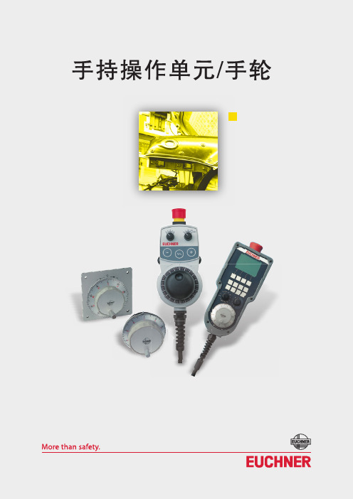
这里一个专利的开关系统确保当开关从3级状态回到1级状态, 在经过2级授权状态时不会让授权功能恢复。授权功能只有当开关完 全复位时,才能再次授权操作。也就是说,只有顺向操作开关(从1 级到2级),授权功能可以激活;而逆向操作开关(从3级到1级), 授权功能受到保护,不能被激活。
手持操作单元的功能和技术
1级 释放状态
2级 授权状态
带有授权功能的手持操作单元
带有授权功能的手持操作单元相当于传统意义上的授权开关。 授权开关是用手操作的控制装置,配合其他功能开关,并对他们 进行正确连续的操作,就可以通过其发出的指令来操控具有危险性的 机械运作。这些授权开关广泛使用在这样的状况下,操作人员必须直 接在机器和设备的危险区域内进行工作。例如,在安装、编程、检测 或维修工作中需要这种授权开关。机器运作指令只有在授权开关的安 全保护下才能传递,一旦动作有危险,指令可随时被取消或中断,另 外还必须有个可锁止的装置(例如电键式开关)来二次保护,这样只 有通过二次单独的操作才能使机器重新开动。为了使操作者能够在一 个机器的危险区域内使机器产生一个运动,还应该另外设置一个可移 动的授权装置。 通过该授权装置,操作者也必须能够使机器停止运动。这个任务 是由授权开关完成的。每个处于危险区域中的人必须随身带有这样一 个授权装置,以便在出现危险时能够及时采取应对措施。
用于手持操作单元的附件 用于所有结构形式的手持操作单元的附件 用于HBA系列手持操作单元的附件 用于HBE/HBL系列手持操作单元的附件
用于手持操作单元的托架
电子手轮 手轮的功能和技术 HKD系列手轮 HKC系列手轮 HKA系列手轮 HWA系列手轮 HWB系列手轮 HWD系列手轮 HWE系列手轮 HWF系列手轮 用于手轮的附件
SAA7324中文资料
The SAA7324 (CD10 II) is a single chip combining the functions of a CD decoder, digital servo and bitstream DAC. The decoder/servo part is based on the SAA737x (CD7) and is software compatible with this design. Extra functions are controlled by use of ‘shadow’ registers (see Section 7.15.3). Supply of this Compact Disc IC does not convey an implied license under any patent right to use this IC in any Compact Disc application.
SAA7324
Servo part Diode signal processing Signal conditioning Focus servo system Radial servo system Off-track counting Defect detection Off-track detection High-level features Driver interface Laser interface Radial shock detector Microcontroller interface Microcontroller interface (4-wire bus mode) Microcontroller interface (I2C-bus mode) Decoder registers and shadow registers Summary of functions controlled by decoder registers 0 to F Summary of functions controlled by shadow registers Summary of servo commands Summary of servo command parameters LIMITING VALUES CHARACTERISTICS OPERATING CHARACTERISTICS (SUBCODE INTERFACE TIMING) OPERATING CHARACTERISTICS (I2S-BUS TIMING) OPERATING CHARACTERISTICS (MICROCONTROLLER INTERFACE TIMING) APPLICATION INFORMATION PACKAGE OUTLINE SOLDERING Introduction to soldering surface mount packages Reflow soldering Wave soldering Manual soldering Suitability of surface mount IC packages for wave and reflow soldering methods DATA SHEET STATUS DEFINITIONS DISCLAIMERS PURCHASE OF PHILIPS I2C COMPONENTS
Amtech Tacky 助焊膏系列安全数据表说明书

Inventec Performance Chemicals USA, LLCSAFETY DATA SHEET (SDS)SECTION 1: PRODUCT AND COMPANY IDENTIFICATIONPRODUCT NAME: Amtech Tacky Paste Flux Series: 200, 400, 500, 600, 4000, SynTECH, WSFC-305L and #61 SYNONYMS:Tacky FluxMANUFACTURER: Inventec Performance Chemicals USA, LLCADDRESS:PO Box 989 Deep River, CT 06417 USAPHONE:860-526-8300FAX:860-526-8243EMERGENCY:Infotrac-(800)535-5035REVISION DATE:December 19, 2014REVISION DATE: 3DOCUMENT NAME:SDS-Tacky Flux-008PRODUCT USE:Bonding solder joints in production and repair of circuit boardsSECTION 2: HAZARDS IDENTIFICATIONCHEMICAL NAME:N/ACHEMICAL FAMILY:MixtureCHEMICAL FORMULA:N/AROUTES OF ENTRY: Inhalation, Ingestion, Skin/Eye ContactGHS:Signal Word: WarningHazard statement(s)H302 Harmful if swallowedH317 May cause an allergic skin reactionH320 Causes eye irritationH335 May cause respiratory irritationPrecautionary statement(s)P102 Keep out of reach of childrenP233 Keep container tightly closedP264 Wash hands thoroughly after handlingP270 Do not eat, drink or smoke when using this productP280 Wear protective gloves/protective clothing/eye protection/face protectionP302+P352 IF ON SKIN: Wash with plenty of soap and waterP305+P351 IF IN EYES: Rinse continuously with water for several minutesP404 Store in a closed containerP501 Dispose of contents/containers in accordance with Federal, State/Provincial, and/or local regulations POTENTIAL HEALTH EFFECTS:EYE CONTACT: May cause moderate irritation. Do not allow material to come in contact with eyes.SKIN CONTACT: May cause moderate skin irritation.INHALATION: May cause irritation to the respiratory tract.INGESTION: Harmful if swallowed. May cause irritation to the mouth, throat, and stomach. May cause abdominal discomfort, nausea, vomiting, and/or diarrhea.CHRONIC: Not established.SECTION 2 NOTES:Inventec Performance Chemicals USA, LLC does not recommend, manufacture, market, or endorse any of its products for human consumption.SECTION 3: COMPOSITION/INFORMATION ON INGREDIENTSIngredient CAS Number Exposure LimitsModified Rosins N/A N/APine Oil Derivatives 8000-41-7 N/AProprietary Ingredients N/A N/AMixed Carboxylic Acids N/A N/ASECTION 3 NOTES:Percentages of individual components are not listed as this information is considered a trade secret.SECTION 4: FIRST AID MEASURESEYES: Flush with plenty of water, contact a physician. If contact lenses can be removed easily, flush eyes without contact lenses. SKIN: Wash affected area with plenty of warm, soapy water. If irritation persists, seek medical attention.INGESTION: Call a physician or Poison Control Center immediately. Do not induce vomiting.INHALATION: Remove to fresh air. If not breathing, seek immediate medical attention.SECTION 5: FIRE-FIGHTING MEASURESEXTINGUISHING MEDIA: Dry chemical, foamSPECIAL FIRE FIGHTING PROCEDURES: Do not use water. Use NIOSH-approved self-contained Breathing Apparatusand full protective clothing if involved in a fire.UNUSUAL FIRE AND EXPLOSION HAZARDS:This product does not present any unusual fire and explosion hazards. SECTION 6: ACCIDENTAL RELEASE MEASURESACCIDENTAL RELEASE MEASURES: If material spills or leaks, collect and place into a properly labeled waste container. Remove traces of tacky flux using cloth rags or paper towels moistened with Isopropyl Alcohol. Follow on-site personal protective equipment recommendations.SECTION 6 NOTES:See Sections 2, 4, and 7 for additional information.SECTION 7: HANDLING AND STORAGEHANDLING/STORAGE: Keep containers tightly closed when not in use. Use care to avoid spills. Avoid inhalation of fumes or dust. Avoid contact with eyes, skin, and clothing.OTHER PRECAUTIONS: Empty containers may retain product residues in vapor, liquid, and/or solid form. All labeled hazard precautions should be observed.WORK HYGIENIC PRACTICES: Cosmetics/Food/Drink/Tobacco should not be consumed or used in work areas. Always wash hands after handling material and before applying or using cosmetics/food/drink/tobacco.SECTION 7 NOTES:For industrial use only.SECTION 8: EXPOSURE CONTROLS/PERSONAL PROTECTIONVENTILATION: Provide sufficient mechanical (general and/or local exhaust) ventilation to maintain exposure below TLVs. RESPIRATORY PROTECTION: Use with adequate ventilation.EYE PROTECTION: Use with appropriate safety glasses.SKIN PROTECTION: Protective gloves and clothing should be worn when handling material. Wash hands thoroughly with soap and water upon leaving the work area.SECTION 9: PHYSICAL AND CHEMICAL PROPERTIESAPPEARANCE: Clear, White, or Yellow to Dark Amber gelODOR: Mild odorODOR THRESHOLD: Not establishedpH as SUPPLIED: N/ASECTION 9: PHYSICAL AND CHEMICAL PROPERTIES (continued)MELTING POINT: Not establishedFREEZING POINT: Not establishedINITIAL BOILING POINT: Not establishedBOILING RANGE: Not establishedFLASH POINT: Not establishedEVAPORATION RATE: Not establishedFLAMMABILITY (solid): Not establishedUPPER/LOWER FLAMMABILITY: Not establishedUPPER/LOWER EXPLOSIVE LIMITS:Not establishedVAPOR PRESSURE (mmHg): N/A (°F/°C)VAPOR DENSITY (AIR = 1): N/A (°F/°C)RELATIVE DENSITY: Not establishedSOLUBILITY IN WATER: PartiallyPARTITION COEFFICIENT (n-octanol/water): Not establishedAUTOIGNITION TEMPERATURE: Not establishedDECOMPOSITION TEMPERATURE: Not establishedVISCOSITY: N/A (°F/°C)SECTION 10: STABILITY AND REACTIVITYSTABILITY: StableCONDITIONS TO AVOID (STABILITY): Freezing temperatures. High temperatures. INCOMPATIBILITY (MATERIAL TO AVOID): Strong oxidizing materialsHAZARDOUS DECOMPOSITION/BY-PRODUCTS: Harmful organic fumes and toxic oxide fumes may form at elevatedtemperatures.POSSIBILITY OF HAZARDOUS REACTIONS: Will not occurSECTION 11: TOXICOLOGICAL INFORMATIONACUTE TOXICITY: Not availableSKIN CORRISION/IRRITATION: Not establishedSERIOUS EYE DAMAGE/IRRITATION: Not availableRESPIRATORY OR SKIN SENSITIZATION: Not establishedGERM CELL MUTAGENICITY: Not availableCARCINOGENICITY: Not availableREPRODUCTIVE TOXICITY: Not availableSTOT-SINGLE EXPOSURE: Not availableSTOT-REPEATED EXPOSURE: Not availableASPIRATION HAZARD: Not availableSECTION 12: ECOLOGICAL INFORMATIONTOXICITY: Product not testedPERSISTENCE AND DEGRADIBILITY: Product not testedBIOACCUMULATIVE POTENTIAL: Product not testedMOBILITY IN SOIL: Product not testedOTHER ADVERSE EFFECTS: Product not testedSECTION 13: DISPOSAL CONSIDERATIONSWASTE DISPOSAL METHOD: Scrap and waste solder should be stored in a dry, sealed container for later disposal. Disposal must be in accordance with Federal, State/Provincial, and Local Regulations.SECTION 14: TRANSPORT INFORMATIONTransport in accordance with applicable regulations and requirements.UN Number: Not availableUN Proper Shipping Name: Not availablePackaging Group:Not applicableEnvironmental Hazards:NoneTRANSPORT HAZARD CLASSES:US DOT Hazardous Material Classification: Tacky Flux is not listed as a DOT hazardous materialWater Transportation: Tacky Flux is not listed as a hazardous materialIATA Hazardous Material Classification: Tacky Flux is not listed as IATA hazardous materialSECTION 15: REGULATORY INFORMATIONAll ingredients used to manufacture this product are listed on the EPA TSCA Inventory.U.S. FEDERAL REGULATIONS: Not regulatedSTATE REGULATIONS: Not regulatedINTERNATIONAL REGULATIONS: Not regulatedSECTION 16: OTHER INFORMATIONHMIS Rating: Health=1 Flammability=1 Physical Hazard=0 Personal Protection=X KEY:N/A: Not applicableGHS: Global Harmonized SystemOSHA: Occupational Safety and Health AdministrationACGIH: American Conference of Governmental Industrial HygienistsNTP: National Toxicology ProgramIARC: International Agency for Research on CancerCAS: Chemical Abstract ServiceNIOSH: National Institute for Occupational Safety & HealthSTOT: Specific target organ toxicityTLV: Threshold limit valueUS DOT: United States Department of TransportationDOT: Department of TransportationIATA: International Air Transport AssociationEPA:Environmental Protection AgencyTSCA:Toxic Substance Control ActHMIS:Hazardous Material Identification SystemPREPARATION INFORMATION:This update supersedes all previously released documents.PREPARED BY: Wendy W. GesickAPPROVED BY: Leigh W. GesickDISCLAIMER:The information contained herein is based on data considered to be accurate but does not purport to be all-inclusive and shall be used only as a guide. No warranty is expressed or implied regarding the accuracy of this data and Inventec Performance Chemicals USA, LLC shall not be held liable for any damage resulting from any handling or contact with the above product. Liability is expressly disclaimed for loss or injury arising out of use of this information or the use of any materials designated. This material is not for resale, unauthorized distribution, or personal use.。
6N134中文资料

6N134中⽂资料FeaturesDual Marked with Device Part Number and DSCC Drawing NumberManufactured and Tested on a MIL-PRF-38534 Certified LineQML-38534, Class H and K Five Hermetically Sealed Package Configurations Performance Guaranteed over -55°C to +125°C ? High Speed: 10 M Bit/sCMR: > 10,000 V/µs Typical 1500 Vdc Withstand Test Voltage2500 Vdc Withstand Test Voltage for HCPL-565X High Radiation Immunity 6N137, HCPL-2601, HCPL-2630/-31 Function Compatibility ? Reliability DataTTL Circuit CompatibilityApplicationsMilitary and SpaceHigh Reliability SystemsTransportation, Medical, and Life Critical SystemsLine ReceiverVoltage Level ShiftingIsolated Input Line Receiver Isolated Output Line Driver Logic Ground Isolation Harsh Industrial EnvironmentsIsolation for Computer,Communication, and Test Equipment SystemsDescriptionThese units are single, dual and quad channel, hermetically sealed optocouplers. The products are capable of operation and storage over the full military temperature range and can be purchased as either standard product or with full MIL-PRF-38534 Class Level H or K testing or from the appropri-ate DSCC Drawing. All devices are manufactured and tested on a MIL-PRF-38534 certified line and are included in the DSCC Quali-fied Manufacturers List QML-38534 for Hybrid Microcircuits.Quad channel devices areavailable by special order in the 16 pin DIP through hole packages.Truth Table(Positive Logic)Multichannel DevicesInput Output On (H)L Off (L)HFunctional DiagramMultiple Channel Devices AvailableSingle Channel DIP Input Enable Output On (H)H L Off (L)H H On (H)L H Off (L)LH*See matrix for available extensions.Hermetically Sealed, High Speed,High CMR, Logic Gate Optocouplers Technical Data6N134*81028HCPL-563X HCPL-663X HCPL-565X 5962-98001HCPL-268K HCPL-665X 5962-90855HCPL-560XCAUTION: It is advised that normal static precautions be taken in handling and assembly of this component to prevent damage and/or degradation which may be induced by ESD.V CC V OUTV E GNDThe connection of a 0.1 µF bypass capacitor between V CC and GND is recommended.Selection Guide–Package Styles and Lead Configuration OptionsPackage16 Pin DIP 8 Pin DIP 8 Pin DIP 8 Pin DIP 16 Pin Flat Pack 20 Pad LCCC Lead Style Through Hole Through Hole Through Hole Through Hole Unformed Leads Surface MountChannels 212242Common Channel V CC , GND None V CC , GND V CC , GND V CC , GND None WiringWithstand Test Voltage 1500 Vdc 1500 Vdc 1500 Vdc 2500 Vdc 1500 Vdc 1500 Vdc Agilent Part # & Options Commercial6N134*HCPL-5600HCPL-5630HCPL-5650HCPL-6650HCPL-6630MIL-PRF-38534, Class H 6N134/883BHCPL-5601HCPL-5631HCPL-5651HCPL-6651HCPL-6631MIL-PRF-38534, Class K HCPL-268K HCPL-560K HCPL-563K HCPL-665K HCPL-663K Standard Lead Finish Gold Plate Gold Plate Gold Plate Gold Plate Gold PlateSolder PadsSolder Dipped Option #200Option #200Option #200Option #200Butt Cut/Gold Plate Option #100Option #100Option #100Gull Wing/Soldered Option #300Option #300Option #300Class H SMD Part #Prescript for all below None 5962-None None None None Either Gold or Solder 8102801EX 9085501HPX 8102802PX 8102805PX 8102804FX 81028032XGold Plate 8102801EC 9085501HPC 8102802PC 8102805PC 8102804FCSolder Dipped 8102801EA 9085501HPA 8102802PA 8102805PA81028032A Butt Cut/Gold Plate 8102801UC 9085501HYC 8102802YC Butt Cut/Soldered 8102801UA 9085501HYA 8102802YA Gull Wing/Soldered 8102801TA 9085501HXA8102802ZA Class K SMD Part #Prescript for all below 5962-5962-5962-5962-5962-Either Gold or Solder 9800101KEX 9085501KPX 9800102KPX 9800104KFX 9800103K2XGold Plate 9800101KEC 9085501KPC 9800102KPC 9800104KFCSolder Dipped 9800101KEA 9085501KPA 9800102KPA 9800103K2AButt Cut/Gold Plate 9800101KUC 9085501KYC 9800102KYC Butt Cut/Soldered 9800101KUA 9085501KYA 9800102KYA Gull Wing/Soldered9800101KTA 9085501KXA 9800102KZA*JEDEC registered part.Each channel contains a GaAsP light emitting diode which isoptically coupled to an integrated high speed photon detector. The output of the detector is an open collector Schottky clamped transistor. Internal shields provide a guaranteed common mode transient immunityspecification of 1000 V/µs. For Isolation Voltage applications requiring up to 2500 Vdc, the HCPL-5650 family is also available. Package styles for these parts are 8 and 16 pin DIP through hole (case outlines P andE respectively), and 16 pin surface mount DIP flat pack(case outline F), leadless ceramic chip carrier (case outline 2).Devices may be purchased with a variety of lead bend and plating options. See Selection Guide Table for details. Standard Microcircuit Drawing (SMD)parts are available for each package and lead style.Because the same electrical die (emitters and detectors) are used for each channel of each device listed in this data sheet, absolute maximum ratings, recommended operating conditions, electrical specifications, and performance characteristics shown in the figures are identical for all parts.Occasional exceptions exist due to package variations and limitations,and are as noted. Additionally, the same package assembly processes and materials are used in all devices. These similarities give justification for the use of data obtained from one part torepresent other parts’ performance for reliability and certain limited radiation test results.Outline Drawings16 Pin DIP Through Hole, 2 ChannelsFunctional DiagramsNote: All DIP and flat pack devices have common V CC and ground. Single channel DIP has an enable pin 7. LCCC (leadless ceramic chip carrier) package has isolated channels with separate VCC and ground connections. All diagrams are “top view.”Leaded Device MarkingLeadless Device MarkingNOTE: DIMENSIONS IN MILLIMETERS (INCHES).COMPLIANCE INDICATOR,*DATE CODE, SUFFIX (IF NEEDED)COUNTRY OF MFR.Agilent CAGE CODE*Agilent DESIGNATORDSCC SMD*PIN ONE/ ESD IDENTAgilent P/N DSCC SMD** QUALIFIED PARTS ONLYCOMPLIANCE INDICATOR,*DATE CODE, SUFFIX (IF NEEDED)DSCC SMD*Agilent CAGE CODE*Agilent DESIGNATORCOUNTRY OF MFR.Agilent P/N PIN ONE/ ESD IDENTDSCC SMD** QUALIFIED PARTS ONLYOutline Drawings (continued)16 Pin Flat Pack, 4 Channels8 Pin DIP Through Hole, 2 Channels 2500 Vdc Withstand Test Voltage20 Terminal LCCC Surface Mount,2Channels8 Pin DIP Through Hole, 1 and 2 Channels0.36 (0.014)NOTE: DIMENSIONS IN MILLIMETERS (INCHES).2.29 (0.090) 2.79 (0.110)NOTE: DIMENSIONS IN MILLIMETERS (INCHES).NOTE: DIMENSIONS IN MILLIMETERS (INCHES).NOTE: DIMENSIONS IN MILLIMETERS (INCHES). SOLDER THICKNESS 0.127 (0.005) MAX.Hermetic Optocoupler OptionsRecommended Operating ConditionsParameterSymbol Min.Max.Units Input Current, Low Level, Each Channel I FL 0250µA Input Current, High Level, Each Channel*I FH 1020mA Supply Voltage, OutputV CC 4.55.5VFan Out (TTL Load) Each ChannelN6*Meets or exceeds DSCC SMD and JEDEC requirements.Absolute Maximum Ratings(No derating required up to +125°C)Storage Temperature Range, T S ...................................-65°C to +150°C Operating Temperature, T A..........................................-55°C to +125°C Case Temperature, T C ................................................................+170°C Junction Temperature, T J ...........................................................+175°C Lead Solder Temperature ...............................................260°C for 10 s Peak Forward Input Current, I F PK , (each channel,≤1 ms duration)......................................................................40 mA Average Input Forward Current, I F AVG (each channel)................20 mA Input Power Dissipation (each channel).....................................35 mW Reverse Input Voltage, V R (each channel).........................................5 V Supply Voltage, V CC (1 minute maximum)........................................7 V Output Current, I O (each channel)...............................................25 mA Output Power Dissipation (each channel). (40)mW Output Voltage, V O (each channel)..................................................7 V*Package Power Dissipation, P D (each channel)........................200 mW*Selection for higher output voltages up to 20 V is available.Single Channel Product OnlyEmitter Input Voltage, V E ...............................................................5.5 VNote enable pin 7. An external 0.01 µF to 0.1 µF bypass capacitor must be connected between V CC and ground for each package type.8 Pin Ceramic DIP Single Channel SchematicESD Classification(MIL-STD-883, Method 3015)HCPL-5600/01/0K ...............................................................(?), Class 16N134, 6N134/883B, HCPL-5630/31/3K, HCPL-5650/51, HCPL-6630/31/3K and HCPL-6650/51/5K.......................(Dot), Class 3Electrical Characteristics (T= -55°C to +125°C, unless otherwise specified)*Identified test parameters for JEDEC registered parts.**All typical values are at V CC = 5 V , T A = 25°C. Recommended Operating Conditions (cont’d.)Single Channel Product Only [10]ParameterSymbol Min.Max.Units High Level Enable Voltage V EH 2.0V CC V Low Level Enable VoltageV EL0.8VElectrical Characteristics, (Contd.) T= -55°C to +125°C unless otherwise specifiedSingle Channel Product Only Low Level I EL V CC = 5.5 V,1, 2, 3-1.45-2.0mA Enable Current V E = 0.5 V High Level V EH 1, 2, 3 2.0V10Enable Voltage Low Level V EL 1, 2, 30.8VEnable Voltage*Identified test parameters for JEDEC registered part.**All typical values are at V CC = 5 V , T A = 25°C.Typical Characteristics, T = 25°C, V = 5 VDual and Quad Channel Product Only Input-Input I I-I 0.5nA Relative Humidity = 45%4Leakage CurrentV I-I = 500 V, t = 5 s Resistance (Input-Input)R I-I 1012V I-I = 500 V 4Capacitance (Input-Input)C I-I0.55pF f = 1 MHz4Notes:1. Each channel.2. All devices are considered two-terminal devices; I I-O is measured between all input leads or terminals shorted together and alloutput leads or terminals shorted together.3. Measured between each input pair shorted together and all output connections for that channel shorted together.4. Measured between adjacent input pairs shorted together for each multichannel device.5. t PHL propagation delay is measured from the 50% point on the leading edge of the input pulse to the 1.5 V point on the leadingedge of the output pulse. The t PLH propagation delay is measured from the 50% point on the trailing edge of the input pulse to the1.5 V point on the trailing edge of the output pulse.6. The HCPL-6630, HCPL-6631, and HCPL-663K dual channel parts function as two independent single channel units. Use the singlechannel parameter limits for each channel.7. CM L is the maximum rate of rise of the common mode voltage that can be sustained with the output voltage in the logic low state(V O < 0.8 V). CM H is the maximum rate of fall of the common mode voltage that can be sustained with the output voltage in the logic high state (V O > 2.0 V).8. This is a momentary withstand test, not an operating condition.9. It is essential that a bypass capacitor (0.01 to 0.1 µF, ceramic) be connected from V CC to ground. Total lead length between bothends of this external capacitor and the isolator connections should not exceed 20 mm.10. No external pull up is required for a high logic state on the enable input.11. The t ELH enable propagation delay is measured from the 1.5 V point on the trailing edge of the enable input pulse to the 1.5 Vpoint on the trailing edge of the output pulse.12. The t EHL enable propagation delay is measured from the 1.5 V point on the leading edge of the enable input pulse tothe 1.5 Vpoint on the leading edge of the output pulse.13. Standard parts receive 100% testing at 25°C (Subgroups 1 and 9). SMD and 883B parts receive 100% testing at 25, 125, and-55°C (Subgroups 1 and 9, 2 and 10, 3 and 11, respectively).14. Parameters are tested as part of device initial characterization and after design and process changes. Parameters are guaranteedto limits specified for all lots not specifically tested.15. Not required for 6N134, 6N134/883B, 8102801, HCPL-268K and 5962-9800101 types.16. Required for 6N134, 6N134/883B, 8102801, HCPL-268K and 5962-9800101 types.17. Not required for HCPL-5650, HCPL-5651 and 8102805 types.18. Required for HCPL-5650, HCPL-5651 and 8102805 types only.Figure 1. High Level Output Currentvs. Temperature.5 VV O * C L INCLUDES PROBE AND STRAY WIRING CAPACITANCE. Figure 4. Test Circuit for t PHL and t PLH .*I +5 V OUTPUT V O MONITORING NODEFigure 7. Test Circuit for Common Mode Transient Immunity and Typical Waveforms.11OUTPUT V OMONITORINGNODET A = +125 °C* ALL CHANNELS TESTED SIMULTANEOUSLY.V CCI O = 25 mAFigure 10. Operating Circuit for Burn-In and Steady State Life Tests. Figure 8. Test Circuit for t EHL and t ELH.Figure 9. Enable Propagation Delayvs. Temperature.MIL-PRF-38534 Class H,Class K, and DSCC SMDTest ProgramAgilent’s Hi-Rel Optocouplers arein compliance with MIL-PRF-38534 Classes H and K. Class Hand Class K devices are also incompliance with DSCC drawings81028, 5962-90855 and 5962-98001.Testing consists of 100% screen-ing and quality conformanceinspection to MIL-PRF-38534./doc/4e2d970a03d8ce2f006623a8.htmlData subject to change.Copyright ? 1999 Agilent TechnologiesObsoletes 5968-4743E5968-9407E (10/00)。
飞利浦 SAA7115 说明书
COMB FILTER • Universal VBI Slicer • Macrovision ®P h i l i p s S e m i c o n d u c t o r sw w w .s e m i c o n d u c t o r s .p h i l i p s .c o mThe SAA7115 provides the front-end digitization and processing of analog video inputs for next-generation set-top boxes,digital televisions,video projectors,personal video,and DVD recorders.A single-chip 9-bit video decoder with 2x-oversampling,the SAA7115provides video capture for a range of applications including advanced large-screen devices such as LCD projectors and HDTVs.Decoding NTSC,PAL and SECAM signals using fully automatic standarddetection,the SAA7115 also includes a pixel accurate H/V scaler,a frame accurate audio clock and an optional square pixel output rate.Designed with service providers in mind the SAA7115complies with Macrovision’s Copy Protection Detect Specification Revision 1.00 and is also well suited for video surveillance systems requiring ultra-fast frame switching.In addition,it is fully pin-to-pin compatible with Philips’ highly successful SAA7114 Video Decoder,making it the ideal solution for a multitude of applications.Product highlightsThe SAA7115 from Philips Semiconductors is a feature-packed video-capture device,offering these major benefits:• Dual 9-bit low noise analog-to-digital converters with 2x-oversampling• Worldwide NTSC/PAL/SECAM decoding with full auto-detection• 6 analog inputs allow flexible combinations of CVBS and S-Video • Best-in-class dynamically adaptive worldwide 4-line comb filter • High performance,pixel-accurate,horizontal and vertical scaler • Automatic VCR detection and optimization • Optional square pixel output rate• Universal VBI data slicer including WST 525/625 T eletext,VPS,US/European Close Captioning (CC),WSS 525/625 (CGMS),US NABTS,VITC 525/625,Gemstar ®1x/2x and Moji Japanese T eletext• Flexible VBI read back via industry standard I 2C-bus• Comprehensive three-level hardware Macrovision ®detection certification• Ultra fast field-lock for advanced video surveillance and security applications• Patented real-time control (RTC) for video editing and time-shift applications• LQFP100 package,pin-to-pin compatible with Philips highly successful SAA7114.T argeting next generation digital video applications For superior performance in today’s PC and consumer video products,as well as tomorrow’s hot new digital video applications,check out the SAA7115 for the following:• PC video capture and editing• Personal Video Recorders (time shifting)• Cable,terrestrial,and satellite set-top boxes • Video projectors • Flat Panel Displays • DVD recorders • Digital televisions• Line doublers and scan converters • Video surveillance and security • Video editing and post production • Video conferencing • Digital VCRs.Multistandard video decoding,scaling,and data processing on one ICWhen a video application demands high quality decoding – flexible scaling and robust data processing – look to the SAA7115 video decoder.Highly integrated and supporting worldwide video standards,the SAA7115 is designed to provide a digital video stream for any video-input application.This includes input to the image port of a VGA controller,for capture to system memory,or to provide digital baseband video to any MPEG encoder,LCD scaler or picture-improvement processor.The SAA7115 features a two-channel analog preprocessing circuit,dual Clock Generation Circuits (CGCs),a digital multistandard decoder and a high-performance pixel-accurate scaler.It accurately decodes all variations of PAL,SECAM,and NTSC signals intostandard ITU-601 compatible component colour values.It accepts CVBS or S-Video (Y+C) from TV or VCR sources as analog inputs – including weak and distorted signals – as well as digital video via an integrated bi-directional expansion port (X Port).At its image port (I Port),the SAA7115 supports scaled 8- or 16-bit output data with auxiliary reference data for interfacing to VGA controllers.For capturing serially coded data in the vertical blanking interval (VBI data),the SAA7115 can use its scaler for interpolating raw video samples to the required data output.Programmable on a line-by-line basis to one of 15 data types,the versatile data slicer can also output through the image port or via the industry standard I 2C-bus.The SAA7115 incorporates frame-locked audio clock generation,to ensure the same number of audio samples is always associated with a frame,or a set of fields.This prevents loss of synchronization between video and audio during capture or playback.Furthermore the second,integrated CGC can be optionally used to enhance this audio clock for an ultra low jitter frame-locked audio clock.Controlled via the I 2C-bus,the SAA7115 offers full write-read capability for all programming registers,at up to 400 kbits/s.RTC OUTPUT RTSx6 ANALOG INPUTS ALLOW FLEXIBLE COMBINATIONS OF CVBS AND S-VIDEOCONTROLPOWER-ON CONTROL AUX PULSE CONTROL XTAL AND VIDEO CLOCKS CHROMAPROCESSINGLUMINANCE PROCESSINGINPUT DATA CONTROLANALOG INPUT PROCESSINGCbCrCDYNAMIC COMBING ENGINESYNCHRONIZATIONSAA7115 VCVBSYADC1ADC2SSSYVideo acquisition and clock generation featuresThe analog pre-processing circuit incorporates source selection,anti-aliasing filters and two low-noise analog-to-digital converters.This sub-system includes input clamps,white-peak control and user-selectable automatic or fully programmable gain control to match specific signal properties.The 9-bit low-noise CMOS analog-to-digital converters provide high performance with oversampling at 27 MHz – twice the ITU-601 standard.On-chip line-locked clock generation also complies with ITU-601and offers free-running capability with horizontal and vertical synchronization generation.• Six analog inputs with internal analog source selectors,e.g.6x CVBS or (2 x YC and 2 x CVBS) or (1 x YC and 4 x CVBS)• T wo built in analog anti-aliasing filters• Dual 9-bit low noise analog-to-digital converters with 2x-oversampling• Fully programmable static gain or automatic gain control (AGC) for the selected CVBS or Y/C channel• Automatic Clamp Control (ACC) for CVBS,Y and C • Switchable white peak control• Requires only one crystal (32.11 MHz or 24.576 MHz) for all standards• Independent gain and offset adjustment for raw data path • On-chip line locked clock generation according to ITU-601• Generation of a frame locked audio master clock to support a constant number of audio clocks per video field • Second onboard analog PLL can be used for:- on-chip line-locked square pixel clock generation for PAL and NTSC square pixel video output or- optional generation of a low jitter frame-locked audio clock from the audio master clock,through reuse of the analog square pixel PLL.Supports audio clock frequencies of 256*fs,384*fs and 512*fs (fs = 32 kHz,44.1 kHz or 48 kHz).• Versatile universal VBI-data decoder,slicer,clock regeneration and byte synchronization for:- WST 525/625 T eletext - VPS- US/European Close Captioning (CC)- WSS 525/625 (CGMS)- US NABTS - VI TC 525/625- Gemstar ®1x/2x- Moji Japanese T eletext.• Flexible VBI read back via industry standard I 2C-bus of the following decoded data types:- US/European Close Captioning (CC)- WSS 525/625 (CGMS)- Gemstar ®1x/2x.Video decoder featuresThe decoder in the SAA7115 is based on the principle ofline-locked clock decoding,yielding the highest quality video with maximum discrimination and automation.The decoder features advanced two-dimensional chrominance/luminance separation using a dynamically adaptive comb filter.• Digital PLL for synchronization and clock generation for all stan-dards and from non-standard video sources,e.g.consumer grade VCR• Automatic detection of 50 Hz / 60 Hz field frequency,and auto-matic recognition of all common broadcast standards • Enhanced horizontal and vertical sync detection• Luminance and chrominance signal processing for PAL BGDHIN,combination-PAL N,PAL M,NTSC M,NTSC-Japan,NTSC 4.43and SECAM (50 Hz / 60 Hz)• High performance 2/4-line comb filter for two-dimensional chrominance/luminance-separation operating with dynamically adaptive comb filter parameters• Independent Brightness Contrast Saturation (BCS) adjustment • User programmable sharpness control • Automatic TV/VCR detection • X-port video output as:- noise shaped 8-bit ITU-656 video or- full 10-bit ITU-656 interface (DC-performance 9-bit).• Certification for detection of copy protected input signals:- according to Macrovision’s Copy Protection Detect Specification Revision 1.00- indicating level of protection.8- or 16-BIT SCALED DATAI 2S CLOCKSI 2CX PORT DATA AND SYNCX PORT I 2C PORTAUDIO CLOCKSMSD805BOUNDARY SCANDECODER OUTPUT CONTROLI PORT OUTPUT FORMATTERAND VIDEO FIFOY Cb CrY Cb Cr SY Cb Cr SUNIVERSAL VBI ENGINEHORIZONTAL PROCESSINGH PORT VIDEO DECODERTASK AND EVENT CONTROLLERBCS CONTROLVERTICAL PROCESSINGSCALER FIR-PREFILTER SAA7115Leading CompetitorSAA7115Leading CompetitorPhilipsSemiconductorsP h i l i p s S e m i c o n d u c t o Additional featuresThe SAA7115 provides flexibility for easy,cost-effective design of today’s video applications.• Generation of an audio serial and left/right (channel) clock signal• Real-time signal port includes continuous line-locked reference clock and real-time status information to support RTC level 3.1 standard • Power-on control• CMOS 3.3 V device with 5 V tolerant digital inputs and I/O ports• Software controlled power-saving standby modes• Programming via serial I 2C-bus;full read-back by an external controller,at a rate of up to 400 kbits/s• Boundary-scan test circuit conforming to IEEE-1149.b1-1994• Available in LQFP100 (SOT407-CD5) package• Pin-to-Pin compatible with Philips Semiconductors SAA7114video decoder.Video scaler featuresThe versatile scaler provides variable horizontal and vertical up- and down-scaling to randomly sized windows and has independent brightness,contrast and saturation control for scaled outputs.Vertical scaling offers linear phase interpolation;6-bit phase accuracy and an accumulating filter for anti-aliasing.Horizontal phase-correct up- and down-scaling means improved signal quality of scaled data,especially for compression and video conferencing applications.This scaling,at 6-bit phase accuracy (1.2 ns step width),uses an anti-aliasing and accumulating filter.• Horizontal and vertical down-scaling and up-scaling to randomly sized windows• Horizontal and vertical scaling range:variable zoom to 1/64(icon) (Note:H and V zoom are restricted by the transfer data rates)• Vertical scaling with linear phase interpolation andaccumulating filter for anti-aliasing (6 bit phase accuracy)• Conversion to square pixel format• Generation of a video output stream with improved synchronization grid at the I-Port• T wo independent programming sets (tasks) for scaler,which define two “ranges” per field or two sequences over frames • Fieldwise switching between decoder and expansion port (X-port) input• Brightness,contrast and saturation controls for scaled outputs.SCB 73November 2001 9397 750 09016The Netherlands。
SWP香港昌晖仪表产品目录
SWP香港昌晖仪表产品目录SWP香港产品目录、SWP-S805-020-23-HL-P昌晖仪表、SWP-ST803-01-12-HL-P-W昌晖仪表、SWP-D935-092-1212-HL-A/M昌晖仪表、SWP-201TC-03-21-A-W昌晖仪表、SWP-S403-02-12-HL昌晖仪表、SWP-S401-02-12-N昌晖仪表、SWP-S804-02-12-HL、SWP-MS808-01-09-N昌晖仪表、SWP-MS809-00-09-N昌晖、SWP-202TR-0808-22-A昌晖仪表、SWP-S403-01-12-HL昌晖仪表、SWP-C803-01-23-HL-P昌晖仪表、SWP-C403-02-12-HL-P昌晖仪表、SWP-201DL-12-22-A-W昌晖仪表、SWP-201TL-02-22-A-W昌晖仪表、SWP-MD806-02-09-N昌晖仪表、SWP-MD809-02-09-N昌晖仪表、SWP-C803-02-08-HL昌晖仪表、SWP-C401-00-12-N昌晖仪表、SWP-ST805-020-03-HL昌晖仪表、SWP-C801-00-12-N-P昌晖仪表、SWP-C801-00-09-N昌晖仪表、SWP-C803-02-08-HL-W昌晖仪表、SWP-S803-01-23-HL昌晖仪表、SWP-C903-01-09-HL昌晖仪表、SWP-C803-01-23-HL-P昌晖仪表、SWP-LCD-P805-010-23-HL昌晖仪表、SWP-C804-02-12-HHLL-P昌晖仪表、SWP-S405-072-09-HL昌晖仪表、SWP-ST823-011-2323-HLHL昌晖仪表、SWP-LCD-NLQ812-010-AGG-HL-P昌晖仪表、SWP-C801-00-12-N-P昌晖、SWP-LK803-81-AAG-HL-2P香港昌晖、SWP-S823-011-0909-HLHL昌晖自动化、SWP-S803-01-12-HL-P昌晖总代理、SWP-MD809-00-23-N昌晖、SWP-T801-02-23-N-P-X昌晖仪表、SWP-MD807-01-23-HL-K昌晖仪表、SWP-MD814-01-23-HL-K昌晖、SWP-C803-21-08-HL昌晖、SWP-8083昌晖仪表、SWP-S835-822-1212-HL昌晖仪表/SWP-D835-012-1212-HL、昌晖仪表总代理SWP-C703-01-09-HL昌晖总代理、SWP-C103-01-23-HL昌晖自动化、SWP-LCD-NLQ812-01-AGG-HL-P昌晖仪表、SWP-LK801-02-C-HL-P昌晖仪表、SWP-C903-01-23-HL昌晖、SWP-X803-0-N-A自动化、SWP-C803-02-23-HL总代理、SWP-LK802-82-AAG-HL-2P国内总代理、WP-C901-00-01-N、WP-C901-00-23-N、SWP-D835-022-1212-HL昌晖自动化仪表有限公司、SWP-D803-01-23-HL-P山东飞创仪表、SWP-D703-02-09-HL昌晖自动化系统有限公司、SWP-C903-01-23-HL-P香港昌晖仪表有限公司、SWP-9036昌晖仪表有限公司、SWP-S823-011-0808-HLHL福州昌晖自动化系统有限公司、SWP-USB128MB福州昌晖自动化仪器仪表有限公司、SWP-C703-01-12-HL昌晖自动化仪表有限公司、SWP-ST803-01-12-HL昌晖仪表、SWP-ST805-022-09-HL昌晖仪表、SWP-C903-01-23-HL-P南京昌晖、SWP-C803-02-23-HL-P、SWP-9035、SWP-C803-01-23-HL、SWP-D805-020-23-HL-P、WP-LEAVC900HLT、SWP-C703-01-03-HL、SWP-ZKH-B3、SWP-P905-040-23-HL、SWP-C801-02-03-N、SWP-C801-02-12-N-P、SWP-MD807-01-23-HL-K、WP-S816-04-23-HL、WP-T804-02-12-HHLL、WP-D925-010-1212-HL-P、SWP-AC-C901-02-05-N、SWP-D905-040-23-HL、SWP-ST805-022-23-HL-P、SWP-S821-000-2323-N、SWP-S801-00-23-N-P-T、SWP-ST803-01-12-HL-P-T、SWP-C803-02-23-HL-P、WP-C804-01-23-HLHL-P、SWP-C803-01-23-HL-P、SWP-LK802-02-AAG-HL-2P、WP-S405-220-09-HL、WP-L804-81-FAN-HL-P、SWP-201IC-12-22-A-D-W、SWP-C903-01-08-HL-P、SWP-S803-01-12-HL-P、SWP-ST803-01-12-HL-P、SWP-S801-00-12-N-P、SWP-LK802-02-AAG-HK-2P、SWP-AC-C401-02-05-N、SWP-C401-02-23-N、SWP-D405-080-23-N、SWP-C403-02-09-HL-W、WP-LEAV-C900HLT、SWP-LK802-02-AAG-HL-2P、SWP-C401-02-12-N-W、SWP-RP-C403-02-24-HL-W、SWP-RP-C403-05-C-HL-W、SWP-LK801-01-A-HC-P、WP-Z403-01-09-HL、WP-Z403-01-12-HL-P、SWP-LK801-02-A-HL-P、SWP-MD806-00-23-N、SWP-202TR-0808-22-A、SWP-C701-00-18-N、SWP-T803-02-12-HL-P-X、SWP-RP-C401-02-24-N-W、SWP-CA102、SWP-C803-01-12-HL、SWP-TC-C403-01-18-H、SWP-AC-C403-01-18-HL、SWP-AC-C401-00-05-N、SWP-S825-020-1212-HL-P、SWP-LK802-82-AAG-HL-2P、SWP-T803-02-12-HL-P-X、SWP-C103-01-23-HL-W、WP-LEAA-C100、SWP-C403-02-23-HL-P、SWP-C901-02-12-N-P、SWP-201IC-12-60-B-W、WP-LC802-82-AAG-HL、WP-D805-820-23-N-T、WP-C803-81-08-HL-P、WP-C403-01-03-HL、SWP-C103-01-23-HH-T、SWP-C401-00-23-N-T、SWP-C901-02-12-N-P、SWP-S805-033-14-HL-P、WP-9035、WP-LEAA-C900、WP-LE3A-C200-3N、WP-LE3V-C200-3N、SWP-LCD-NLR802-02-AAG-HL-2P、SWP-S823-822-1212-HLHL-2P、SWP-S805-822-12-HL-P、SWP-LK801-02-A-HL-P、WP-9035、SWP-LCD-NLQ812-01-AGG-HL-2P、SWP-C804-01-23-HLHL-P、SWP-9035、SWP-S835-010-23-HL、SWP-LCD-NL804-02-AAA-HL-2P-T、WP-6231、SWP-D903-01-23-HL、SWP-C803-02-12-HL-P-T、SWP-LCD-NLQ812-01-AGG-HL-2P、SWP-D905-020-12-N-P、SWP-9083、SWP-8083、SWP-ND805-0230-23-HL-P、SWP-D403-01-23-HL-P、WP-D405-010-09-HL、WP-L803-02-AAG-HL-2P、SWP-X803-0N-A、SWP-D805-020-23-HL-P、SWP-C803-01-23-HL-P、SWP-D401-02-23-N、SWP-D935-010-2323-HL、WP-D804-01-08-HLHL-P、SWP-C101-00-09-N、WP-LC802-02-AAG-HL-2P、SWP-C801-80-23-N、WP-LC802-82-AAG-HL-2P、SWP-AC-C401-02-05-N-P、SWP-D805-02-12(23)-HL、SWP-LCD-P805-020-23-HL、SWP-LK801-01-A-HL-P、SWP-201IC-24-21-B、SWP-S405-022-12-L、SWP-C803-01-23-HL-P、SWP-D821-022-0808-N-2P、WP-D821-022-0808-N-2P、SWP-9034、SWP-9035、SWP-C901-02-12-N-P、WP-C801-00-23-N、SWP-LK802-02-AAG-HL、SWP-C901-80-23-N、SWP-AC-C401-02-05-N、SWP-USB128MB、SWP-LK801-02-A-HL-P、SWP-ST803-01-23-HL-P、SWP-201IC-18-21-B、SWP-C803-01-23-HL-P、SWP-C904-01-23-HHLL、SWP-C904-01-10-HLHL-P、SWP-D905-022-23-HL-P-T、SWP-LCD-D805-020-08-HL、SWP-D915-022-08/12-HL、SWP-D805-020-12-HL、SWP-D935-010-1212-HL、SWP-S405-020-09-HL、SWP-C701-02-12-N、WP-C801-80-12-N-T、SWP-C701-80-23-N-P、SWP-C803-01-23-HL-P、SWP-S804-01-23-HHLL、SWP-D923-021-12/09-HHLL-P、SWP-D903-02-23-HL、WP-D807-01-08-HL-W、SWP-VSR112、SWP-C803-01-23-HL、SWP-C401-00-12-N、SWP-LCD-NLR801-82-A-HL-P、SWP-D935-010-12/12-HL、NJSWP-D923、SWP-C801-00-12-N-W、SWP-ST803-01-23-HL-P、WP-C804-81-12-HL-T、SWP-S403-02-12-HL-P-T、SWP-C401-02-23-N、SWP-RD806-00-23-N 带打印、SWP-NLR802-02-AAG-HL-2P、SWP-C803-02-12-HL、SWP-C803-02-23-HL-P、SWP-LCD-MD814、SWP-D823-011-23/23-HLHL-2P、打印机、SWP-MSR102-1-0/P1/J4/PID/SSR/C2、SWP-C403-01-23-HL-P、SWP-MD814-01-09-HL-W、SWP-RP-C403-01-24-HL-W、SWP-C403-01-23-HL、SWP-C403-01-12-HL-P、SWP-LK801-02-A-HL-P、SWP-D905-022-23-HL-P、SWP-C403-01-18-HL、SWP-D805-020-23-HL、SWP-C403-01-23-HL-P、SWP-D935-020-23-HL、SWP-201TC-06-22-A-T、SWP-MD814-01-09-HL-W、SWP-C401-00-18-W 0-10V 100A、SWP-C403-00-18-HL-W 5V/2.0MPa、WP-LEAV-C680N(1500V/100V)、WP-LEAV-C680N(10V/10V)、WP-LEAV-C680N(100V/100V)、WP-LEAA-C680N(100A/5A)、WP-LEAA-C680N(3000A/5A)、WP-LEAA-C680N(5A/5A)、WP-LE3V-C9803N(500V/500V)、WP-LE3A-C9803N(100A/5A)、SWP-C803-01-23-HL-P、SWP-USB128MB、SWP-TC-C401-00-D-N、SWP-C103-01-23-HL-P、SWP-8083、SWP-C903-01-23-HL-P、SWP-LK801-02-A-HL-P、SWP-TSR108-1-0/USB128MB、SWP-S403-02-23-HL、SWP-C103-01-23-HL-W、SWP-C904-02-23-HHLL、SWP-T51DP3E22M1B3C2 0-6MPa、SWP-MD807-01-08-HL-K-T、WP-L804-81-FAN-HL-P、SWP-C701-02-12-N。
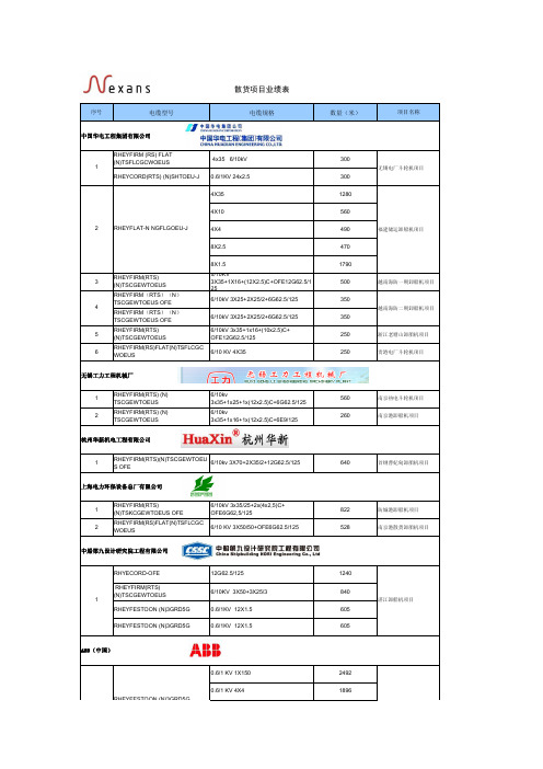
Nexans___售__表
散货项目业绩表序号电缆型号电缆规格数量(米)项目名称RHEYFIRM (RS) FLAT(N)TSFLCGCWOEUS4x35 6/10kV 300RHEYCORD(RTS) (N)SHTOEU-J0.6/1KV 24x2.53004X3512804X105604X44908X2.54708X1.517903RHEYFIRM(RTS)(N)TSCGEWTOEUS 6/10KV3X35+1X16+(12X2.5)C+OFE12G62.5/125500越南海防一期卸船机项目RHEYFIRM (RTS )(N )TSCGEWTOEUS OFE 6/10kV 3X25+2X25/2+6G62.5/125350RHEYFIRM (RTS )(N )TSCGEWTOEUS OFE 6/10kV 3X25+2X25/2+6G62.5/1253505RHEYFIRM(RTS)(N)TSCGEWTOEUS6/10kV 3x35+1x16+(10x2.5)C+OFE12G62.5/125250浙江老塘山卸船机项目6RHEYFIRM(RS)FLAT(N)TSFLCGC WOEUS6/10 KV 4X35250贵港电厂斗轮机项目1RHEYFIRM(RTS) (N)TSCGEWTOEUS 6/10kv3x35+1x25+1x(12x2.5)C+6G62.5/125560南京热电斗轮机项目2RHEYFIRM(RTS) (N)TSCGEWTOEUS6/10kv3x35+1x16+1x(12x2.5)C+6E9/125260南京港卸船机项目1RHEYFIRM(RTS)(N)TSCGEWTOEUS OFE6/10kv 3X70+2X35/2+12G62.5/125640首钢曹妃甸卸船机项目1RHEYFIRM(RTS)(N)TSKCGEWTOEUS OFE 6/10kV 3x35/25+2x(4x2,5)C+OFE6G62,5/125822防城港卸船机项目2RHEYFIRM(RS)FLAT(N)TSFLCGC WOEUS6/10 KV 3X50/50+OFE6G62.5/125528南京港散货卸船机项目RHYECORD-OFE 12G62.5/1251240 RHEYFIRM(RTS)(N)TSCGEWTOEUS6/10KV 3X50+3X25/3840RHEYFESTOON (N)3GRD5G 0.6/1KV 12X1.5605RHEYFESTOON (N)3GRD5G0.6/1KV 12X1.56050.6/1 KV 1X15024920.6/1 KV 4X41896中国华电工程集团有限公司4杭州华新机电工程有限公司无锡工力工程机械厂上海电力环保设备总厂有限公司中船第九设计研究院工程有限公司ABB(中国)1湛江卸船机项目12越南海防二期卸船机项目无锡电厂斗轮机项目福建储运卸船机项目RHEYFLAT-N NGFLGOEU-J RHEYFESTOON (N)3GRD5G0.6/1 KV 4X103700.6/1 KV 4X16288RHEYFESTOON (C)(N)3GRDGC5G (6X(2X1)C)C 580RHEYFESTOON (C)(N)3GRDGC5G 12X2.5 C950RHEYFESTOON (N)3GRD5G 1X2405120RHEYFESTOON (N)3GRD5G 18X1.52560RHEYFESTOON (N)3GRD5G 18X2.51280RHEYFESTOON (N)3GRD5G 1X955120RHEYFESTOON (N)3GRD5G6X(2X1)C 1280RHEYFESTOON (N)3GRD5G 1X1507040RHEYFESTOON (N)3GRD5G 4X25640RHEYFESTOON (N)3GRD5G 1X502560RHEYCORD-OFE M 12G62.5/1251280RHEYFIRM(RTS)(N)TSCGEWTOEUS OFE6/10KV 3X70+2X35/2+12G62.5/125u1040RHEYFIRM(RTS)(N)TSCGEWTOEUS 6/10 KV 3x50/25+2x(6x2.5)C+OFE12G62.5/125340RHEYCORD-OFE M12G62.5/1252204X42004X162001X352006X(2X1)C43218X2.5297RHEYCORD-OFE M12G62.5/125400RHEYCORD(RTS) (N)SHTOEU-J 25X2.5+1X(12E9/125)530RHEYFIRM(RTS)(N)TSCGEWTOEUS OFE 6/10kV 3X50+3X25/3380RHEYFIRM(RTS)(N)TSCGEWTOEUS6/10kV 3X35+3X25/31503RHEYFIRM(RTS)(N)TSCGEWTOEUS6/10KV 3X35+2X25/2 OFE 6G62.5/125870新加坡PSA STS 项目4RHEYFIRM(RTS)(N)TSCGEWTOEUS OFE6/10kV 3x70+2x35/2+6 OFE720韩国釜山STS 项目5RHEYFIRM(RTS)(N)TSCGEWTOEU S OFE 3.6/6kV 3x120 + 2 x 70/2 + 1FO 18E(9/125mm SM )1472新加坡PSA STS 项目1RHEYFIRM(RTS)(N)TSCGEWTOEUS 6/10KV3X185+1X95+2X(2X2.5)C+1X(6G62.5/125)6402RHEYFIRM(RTS)(N)TSCGEWTOEUS6/10KV3X185+1X95+2X(2X2.5)C+1X(6G62.5/125)28054817宝钢罗泾280T行车项目扬州江都船厂龙门吊项目中船江南重工股份有限公司上海振华港机(集团)股份有限公司1印度卸船机项目大连重工.起重集团有限公司2RHEYFESTOON (N)3GRD5G 宝钢湛江码头卸船机项目11威海卸船机项目RHEYFESTOON (N)3GRD5G集装箱项目业绩表序号电缆型号电缆规格数量(米)项目名称1RHEYCORD(BS) YSLZ3SSOE-J 300/500 36X2.5471岳阳RTG 项目RHEYFIRM(RTS)(N)TSCGEWTOEUS8.7/15kV 3X25+3X25/3760RHEYCORD(BS) YSLZ3SSOE-J 300/500 36X2.5424RHEYCORD-OFE M 12G62.5/125400RHEYFIRM(RTS)(N)TSCGEWTOEUS6/10kV 3X25+3X25/3380RHEYCORD(BS) YSLZ3SSOE-J 300/500 36X2.5197RHEYCORD-OFE M12G62.5/125190RHEYCORD(RTS)(N)SHTOEU-J 0.6/1 KV 3x120+3x70/32240RHEYCORD(RTS)(N)SHTOEU-J0.6/1 KV 3x120+3x70/31280RHEYCORD(RTS)(N)SHTOEU-J 0.6/1 KV 3x150+3x70/34480RHEYCORD(RTS)(N)SHTOEU-J0.6/1 KV 3x150+3x70/325605RHEYCORD(RTS) (N)SHTOEU-J SPREADER 44x2.5166福州RTG 项目6RHEYCORD(RTS) (N)SHTOEU-J3x120+3x70/32100韩国仁川STS 项目RHEYFIRM(RTS)(N)TSCGEWTOEUS3.6/6 KV 3x25+3x25/3960RHEYCORD(BS) YSLZ3SOE-J 300/500V 42x2.5110RHEYFESTOON(N)3GRD5G0.6/1KV 4X25258RHEYFESTOON(N)3GRD5G 0.6/1KV 24X2.5258RHEYFESTOON(N)3GRD5G 0.6/1KV 6X(2X1)C 258RHEYCORD OFE M12G62.5/125278RHEYFIRM(RTS)(N)TSCGEWTOEUS6/10 KV 3x50+2x25/2+6E9/1252502RHEYCORD(RTS)(N)SHTOEU-J SPREADER0.6/1KV 56x2.5552RHEYFESTOON(N)3GRD5G0.6/1KV 5X251146RHEYFESTOON(N)3GRD5G 0.6/1KV 18X2.51337RHEYFESTOON(N)3GRD5G 0.6/1KV 6X(2X1)C 1337RHEYCORD OFE M12G62.5/1251400RHECORD(RTS)(N)SHTOEU-J0.6/1 KV 3X95+2X50/2+(2X2.5)C 5400RHEYCORD(BS) YSLZ3SOE0.6/1kv 36X2.545610H07RNF,RHEYFLEX592887深圳大铲湾RTG 项目RHEYFIRM(RTS)(N)TSCGEWTOEUS12/20kV 3X25+3X25/31160上海振华港机(集团)股份有限公司2津唐港1期STS 项目3津唐港2期STS 项目4天津欧亚E-RTG 项目7南通港STS 项目8宁波梅山STS 项目9宁波梅山E-RGT 项目大连重工.起重集团有限公司RHEYCORD(BS) YSLZ3SSOE-J 300/500 54X2.5320RHEYFESTOON(C) (N)3GRDGC5G3X16+3X16/3 C 2560RHEYFESTOON (N)3GRD5G 12X2.52560RHEYFESTOON (N)3GRD5G 6X(2X1)C 1280RHEYFESTOON (N)3GRD5G 4X101280RHEYCORD-OFE M12G62.5/125740RHEYFIRM (N)TSCGEWTOEUS OFE8.7/15 kV 3x35+2x25/2+12G(62.5/125)570RHEYCORD(RTS) (N)SHTOEU-J spreader44x2.51653RHEYFIRM (RTS)(N)TSCGEWTOEUS OFE 6/10kV 3x95+2x50/2+12E 9/125µ470印度卸船机项目RHEYFESTOON(N)3GRD5G 0.6/1KV 12x2.52240RHEYFESTOON(C)(N)3GRDGC5G 0.6/1KV 3X25+3X16/31120RHEYFESTOON(N)3GRD5G 0.6/1KV 4X10560RHEYFESTOON(N)3GRD5G0.6/1KV 4X161120RHEYFESTOON(N)3GRD5G 0.6/1KV 1X50560RHEYFESTOON(N)3GRD5G 0.6/1KV 6X(2X1)C 1120RHEYCORD-OFE M 12G62.5/125600RHEYFIRM(RTS)(N)TSCGEWTOEUS 12/20KV 3X25+3X25/31200RHEYCORD(BS)YSLZ3SOE-J0.6/1KV 54x2.53205RHEYFIRM (RTS )(N )TSCGEWTOEUS8.7/15kV 3X25+3X25/31800泰国曼谷港备件项目RHEYFESTOON(N)3GRD5G 0.6/1KV 12x2.52240RHEYFESTOON(C)(N)3GRDGC5G 0.6/1KV 3X25+3X16/3c 1120RHEYFESTOON(N)3GRD5G 0.6/1KV 4X10560RHEYFESTOON(N)3GRD5G0.6/1KV 4X161120RHEYFESTOON(N)3GRD5G 0.6/1KV 1X50560RHEYFESTOON(N)3GRD5G 0.6/1KV 6X(2X1)C 1120RHEYCORD-OFE M 12G62.5/125600RHEYFIRM(RTS)(N)TSCGEWTOEUS 8.7/15KV 3x25+3x25/31000RHEYCORD(BS)YSLZ3SOE-J 0.6/1KV 54x2.5320RHEYCORD(RTS)(N)SHTOEU-J SPREADER0.6/1 kv 44x2.5165RHEYFIRM (N)TSCGEWTOEUS OFE8.7/15 kV 3x35+2x25/2+6FO5701BUFLEX X'Prem6/10(12)KV 3X35+3X1033602RHEYCORD(BS)YSLZ3SOE-J42X2.5465659732中铁山桥集团工程机械有限公司中铁集装箱轨道吊项目6泰国曼谷港三期STS项目7东营港二期多用途门机项目4泰国曼谷港二期STS 项目泰国曼谷港一期STS 项目12东营港一期多用途门机项目。
saa7121中文资料
GM7121C型(视频解码电路)1概述视频编码电路主要实现接收8位CCIR656格式的YUV数据,(例如MPEG解码数据),并编码成亮度Y和色度信号C,以及合成CVBS信号,经过D/A转换后输出。
基本的编码功能包括副载波产生,色差信号调制,同步信号内插。
主要应用在视频处理,军事图像处理。
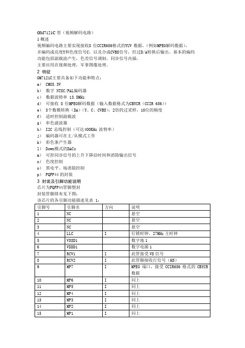
2 特征GM7121C主要具备如下功能和特点:a) CMO3.3Vb)数字 NTSC/PAL编码器c)数据波特率 13.5MHzd)可接收 8位MPEG解码数据(输入数据格式为CBYCR(CCIR 656))e) 3个数模转换(DA)(Y、C、CVBS),2倍的过采样,10位的精度f)适时控制副载波g)串色滤波器h) I2C总线控制(可达400KHz波特率)j)编码器可在主/从模式工作k)彩色条产生器l) Down模式的DACsm)可控同步信号的上升下降沿时间和消隐输出信号n)色度控制o)黑电平、场消隐控制p) PQFP44的封装3 封装及引脚功能说明芯片为PQFP44管脚塑封封装管脚排布见下图:该芯片的各引脚功能描述见表 1:引脚号引脚名方向说明1 NC 悬空2 NC 悬空3 NC 悬空4 LLC I 行锁时钟,27MHz主时钟5 VSSD1 数字地16 VDDD1 数字电源17 RCV1 I 此管接受VS信号8 RCV2 I 此管脚接收行信号(HS)9 MP7 I MPEG端口,接受CCIR656格式的CBYCR数据10 MP6 I 同上11 MP5 I 同上12 MP4 I 同上13 MP3 I 同上14 MP2 I 同上15 MP1 I 同上16 MP0 I 同上17 VDDD2 数字电源218 VSSD2 数字地219 RTCI I 适时控制输入;如果LLC时钟由SAA7111或SAA7151提供,RTCI信号应该链接到对应解码器的RTCO端口,以提高信号质量20 NC 悬空21 SA I I2C总线地址选择输入管脚;、为低电平:从地址为88H为高电平:从地址为8CH22 NC 悬空23 NC 悬空24 C O 色差信号模拟输出25 VDDA1 模拟电源1,供给C路DA电源26 NC 悬空27 Y O 亮度信号模拟输出28 VDDA2 模拟电源2 供给Y路DA电源29 NC 悬空30 CVBS O CVBS符合信号模拟输出31 VDDA3 模拟电源3,供给CVBS路DA电源32 VDDA1 模拟地133 VDDA2 模拟地234 XTAL0 O 晶振输出35 XTAl1 I 晶振输入36 VDDA4 模拟电源4,提供给晶振和参考电压37 XCLK O 晶振时钟输出38 VSSD3 数字地339 VDDD3 数字电源340 RSTN I 复位输入,低有效41 SCl I I2C串行时钟输出42 SDA I/O I2C串行数据端口43 NC44 NC4 功能描述视频编码器对数字亮度和色差信号进行编码,并转换成模拟复合电视信号CVBS和模拟分离电视信号S-video信号输出。
LOC111中文资料
LOC111中⽂资料LOC111Linear OptocouplersApplicationsFeaturesDescriptionApprovalsOrdering Information Pin ConfigurationLOC111 is a linear optocoupler for use in telecom, med-ical and power supply isolation circuits. They are available in 8 pin DIP , surface mount or flatpack packages.Modem Transformer Replacement With No Insertion LossDigital Telephone IsolationPower Supply Feedback Voltage/Current Medical Sensor Isolation Audio Signal InterfacingIsolation of Process Control TransducersUL Recognized: File Number E76270CSA Certified: File Number LR 43639-10BSI Certified:BS EN 60950:1992 (BS7002:1992)Certificate #:7344 BS EN 41003:1993Certificate #:73448 Pin Flatpack or DIP PAckage (PCMCIA Compatible)?Couples Analog and Digital Signals ?Wide Bandwidth (>200kHz)?High Gain StabilityLow Input/Output Capacitance Low Power Consumption 0.01% Servo Linearity THD 87dB TypicalMachine Insertable, Wave SolderableSurface Mount and Tape Reel Versions Available VDE CompatibleLOC111 PinoutDLED +LED +V cc 1I1NC NC +V cc 2I 2LOC111Absolute Maximum Ratings are stress ratings. Functional operation of the device at these or any other conditions beyond those indicated in the operational sections of this data sheet is not implied. Exposure of the device to the absolute maximum ratings for an extended period may degrade the device and effect its reliability.Absolute Maximum Ratings (@ 25o C)Electrical Characteristics2Derate Linearly 6.67 mW/°CK3 Sorted Bins Bin A= 0.550-0.605Bin B = 0.606-0.667Bin C = 0.668-0.732Bin D = 0.733-0.805Bin E = 0.806-0.886Bin F = 0.887-0.974Bin G = 0.975-1.072Bin H = 1.073-1.179Bin I = 1.180-1.297Bin J= 1.298-1.426The LOC110/LOC111/LOC112 are shipped in anti-static tubes of 50pieces. Each tube will contain one K3 sorted bin.Bin designation marked on each device (A-J).Orders for the LOC110 product will be shipped using bins available at the date of the order. Any bin (A-J) can be shipped.For customers requiring selected bins D E F G we offer part num-bers LOC111 or LOC112.LOC111Performance Data*The Performance data shown in the graphs above is typical of device performance. For guaranteed parameters not indicated in the written specifications, please contact our application department.LOC111Dimensionsmm (inches)Mechanical DimensionsCPC7581 Mechanical DimensionsDimensionsmm(inches)CLARE LOCATIONSClare Headquarters78 Cherry Hill DriveBeverly, MA01915Tel: 1-978-524-6700Fax: 1-978-524-4900Toll Free: 1-800-27-CLARE Clare Micronix Division 145 ColumbiaAliso Viejo, CA92656-1490 Tel: 1-949-831-4622Fax: 1-949-831-4628SALES OFFICES AMERICASAmericas HeadquartersClare78 Cherry Hill DriveBeverly, MA01915Tel: 1-978-524-6700Fax: 1-978-524-4900Toll Free: 1-800-27-CLARE Eastern RegionClareP.O. Box 856Mahwah, NJ 07430Tel: 1-201-236-0101Fax: 1-201-236-8685Toll Free: 1-800-27-CLARE Central RegionClare Canada Ltd.3425 Harvester Road, Suite 202 Burlington, Ontario L7N 3N1 Tel: 1-905-333-9066 Fax: 1-905-333-1824Western RegionClare1852 West 11th Street, #348 Tracy, CA95376Tel: 1-209-832-4367Fax: 1-209-832-4732Toll Free: 1-800-27-CLARE CanadaClare Canada Ltd.3425 Harvester Road, Suite 202 Burlington, Ontario L7N 3N1 Tel: 1-905-333-9066 Fax: 1-905-333-1824EUROPEEuropean HeadquartersCP Clare nvBampslaan 17B-3500 Hasselt (Belgium)Tel: 32-11-300868Fax: 32-11-300890FranceClare France SalesLead Rep99 route de Versailles 91160 ChamplanFranceTel: 33 1 69 79 93 50Fax: 33 1 69 79 93 59 GermanyClare Germany Sales ActiveComp Electronic GmbH Mitterstrasse 1285077 ManchingGermanyTel: 49 8459 3214 10Fax: 49 8459 3214 29ItalyC.L.A.R.E.s.a.s.Via C. Colombo 10/AI-20066 Melzo (Milano) Tel: 39-02-95737160Fax: 39-02-95738829 SwedenClare SalesComptronic ABBox 167S-16329 Sp?ngaTel: 46-862-10370Fax: 46-862-10371United KingdomClare UK SalesMarco Polo HouseCook WayBindon RoadTauntonUK-Somerset TA2 6BG Tel: 44-1-823 352541Fax: 44-1-823 352797ASIA PACIFICAsian HeadquartersClareRoom N1016, Chia-Hsin, Bldg II,10F, No. 96, Sec. 2Chung Shan North RoadTaipei, Taiwan R.O.C.Tel: 886-2-2523-6368Fax: 886-2-2523-6369/doc/0fd841f2770bf78a64295400.html Worldwide Sales OfficesSpecification: DS-LOC111-R6Copyright 2001, Clare, Inc.All rights reserved. Printed in USA.02/23/01Clare cannot assume responsibility for use of any circuitry other than circuitry entirely embodied in this Clare product. No circuit patent licenses nor indemnity are expressed or implied. Clare reserves the right to change the specification and circuitry, with-out notice at any time. The products described in this document are not intended for use in medical implantation or other direct life support applications where malfunction may result in direct phys-ical harm, injury or death to a person.。
萨维科AC-IR-3Fq地址可控 传统型红外火焰探测器说明书

Addressable/ConventionalIR Flame DetectorSalwico AC-IR-3FqPart no.5200236-00ASystem:Depends on base.See Datasheet for:5200235-00A Salwico AC-IR-3Fq Conventional Base and 5200237-00ASalwico AC-IR-3Fq Addressable BaseGeneral DescriptionThe AC-IR-3Fq is a triple frequency infrared flame detector produced using the latest inmanufacturing technology.It is supplied with an array of advanced features,making it ‘better by design’.The detector uses infrared elements suitable for the detection of smokeless combustible liquid and gas fires,as well as smoke-forming open fire involving carbonaceous materials as contained in wood,plastics,gases,oil products etc.The fire evaluation process is done by triple infrared (3Fq)sensor,protected by a sapphire glass filtering >6.0µm wavelength radiation.The sensor measures the hot carbon dioxide in a specific flame wavelength;the B and C sensors simultaneously measure the interference radiation in near wavelengths.This technique together with intelligent signal processing through microprocessor and custom algorithms,achieves excellent detection reliability while maintaining the highest immunity to interference radiation and sunlight.Features•Triple frequency IR detector •Low current draw•Suitable for installation in damp environment •Easy maintenance •Remote LED option•Approved to UNI EN54-10Ed.2002T estingFor functional test,use Salwico IR T est lamp,part no.5100553-00A.Due to the detectors high immunity to unwanted alarms,it is difficult to test the detector without the IR test lamp.T est with gas torchA test with real fire can also be conducted using gaseous combustible,such as butane,propane,LPG etc.,by using a gas torch.Adjust to obtain a flame of about 25cm in length.The detection distance,with Class 3detector,is about 2 m.T o obtain a red flame,it is necessary to partially obstruct the nozzle adjustment air holes.NOTE!Correction factor in the table is referred to Ethyl alcohol.FuelDistance correction factor Ethyl alcohol puriss. 1.0Petrol (Heptan purum) 1.5Diesel oil (gas oil)0.8Kerosene (jet fuel A1) 1.0Methyl alcohol purum 0.8Acetone1.5DataElectrical Specifications Conventional Mode (incl.Base)Working voltage 14-30VDC Working current 0.45mA Alarm currentMax 30mAElectrical Specifications Addressable Mode (incl.Base)Working voltage 22-38VDC Working current 0.6mA Alarm current 1mA Current when short circuited12mAEnvironmental SpecificationsApplication T emperatureRange-25°C to+75°CHumidity Up to95%Mechanical InformationHeight69mm(including base)Diameter103mmWeight250g±5%Weight with IP65Base380g±5%Wire Gauge for T erminals 2.5mm2Colour White RAL9010Material Polycarbonate FlameRetarded Cl.UL94V0IP Rating Depends on baseCertified according to0474/yyyyyyyy=year of productionDetector Base5200235-00A Salwico AC-IR-3Fq Conventional Base5200237-00A Salwico AC-IR-3Fq Addressable Base5100874-00A AC-IR-3Fq Rugged Addressable BaseT est Equipment5100553-00A Salwico IR T est lampInstallationBase alternatives:•T o reach IP65,use conventional or addressablebase with bayonet and locking screws.NOTE!The plastic covering the screw holes(diaphragm)has to be removed first.A)Diaphragm•T o reach IP67or IP66,use rugged base.Do not remove the plastic covering the screwholes(diaphragm)when using this base.If diaphram is broken,tighten the screw byusing a bolt and a washer.Certain factors need to be considered whendesigning an installation:•The sensors should not be mounted exposedto direct or reflected sunlight.•The sensors should be mounted so thatobjects do not block their field-of-view(FOV).This includes glass,Plexiglas and other visiblytransparent materials.Contact Consilium formore information.•Whenever possible,sensors should bemounted so their ranges and fields-of-viewoverlap.•Sensors should be mounted so their FOVcannot be choppered by moving machinery orhuman operators during normal operationswithin the area.Therefore they should beinstalled as high as possible or on the ceiling.•The detector window should not be exposedto hot or cold intermittent airflow which couldchange the temperature of the detector itselfor detector FOV background.•T o ensure optimum sensitivity andperformance,sensors should be mounted sothey do not point directly at hot surfaces:ifthis is necessary first follow procedure toensure no chopper is present.•When monitoring hot spots(eg engine exhaust)the minimum distance should be atleast3meters.If not possible,move thedetectors optical FOV so it is not completelydirected towards the hot area to control.•The sensors should be mounted so that they are easily and safely accessible for inspectionand maintenance.•If mechanical,high-temperature damage,or window contamination is likely to occur in the installed location,the sensor should beprotected.However the protection methodcannot obstruct the sensors FOV with anymaterial,including visibly transparent materials, such as glass and Plexiglas.•The sensor can be mounted in anyorientation,as long as captive screws areremoved or can be removed.•Mounting the sensor so that it pointsdownwards is recommended as this generally results in minimal window contamination.•The best form of room monitoring is achieved by mounting the detector high in the cornerof the room with detector inclined towardsthe floor.Angle of inclination of detectoraxis=45°and lateral angle=45°.•In the case of ceiling mounting it is necessary to calculate the coverage area according tothe installation height.In this installation therecan be a slight obstruction of vision by smoke from the fire.For this reason it is advisable that the detector is mounted below the ceiling atabout10%of the room height.•Care must be taken to avoid that sensor installation exceeds environmental approvalssuch as temperature,shocks,vibrations.•Care must be taken to avoid that sensor installation exceeds electromagneticinterference approval:in particular installdetectors in places out-of-reach of personnel(including contractors and crew members).•It is important NOT to leave any extra cable slack when installing this detector.•Cable shield shall be connected to the ground on one side only.•The DIP-Switch Setting recommended by Consilium is to turn Sw.No.2ON for thehighest sensitivity.For more details,seeSettings.For more details,see Flame Detector Installation manual5100512.Angle ofReceptionDimensions(mm)SettingsS1DIP-SwitchsetupFigure 1.DIP-Switch Setting.Use the 4-ways Dip-switch S1to set the detectoras Conventional or Addressable and preset sensitivity threshold (Class).Angle of Reception ±42°in all configurations.Table 1.DIP-Switch SettingSensitivit y class Sw.No.1Sw.No.2Sensitivity Class 1*OFFONHigh,up to 25mSensitivit y class Sw.No.1Sw.No.2Sensitivity Class 2ON OFF Medium,up to 17m Class 3**OFFOFFLow,up to 12mTable 2.Conventional Mode Mode Sw.No.3Sw.No.4ConventionalONONOnly when used with Base 5200235-00A.Table 3.Addressable Mode ModeSw.No.3Sw.No.4Addressable**OFFOFFOnly when used with Base 5200237-00A.*Recommended setting by Consilium **Default factory settingDirectional sensitivity and cover area。
基于SAA7114H的图像无级缩放功能的实现

总第169期2008年第7期 舰船电子工程S hi p E lectronic Engineering V ol .28N o .7 162 基于SAA 7114H 的图像无级缩放功能的实现3徐小梅 冯彬彬 王 珩(武汉数字工程研究所 武汉 430074)摘 要 在实际工程应用中,对图像无级缩放功能的需求日益增多。
由此,介绍一种已经在实际应用中得到验证的图像无级缩放功能的实现方案。
该方案通过对单片机的控制,完成解码器SA A 7114H 和其他器件之间的I 2C 总线通讯,同时,在FPGA 内部集成全部控制逻辑。
关键词 SAA 7114H;解码;图像;无级缩放;M CU FPGA 中图分类号 T P391.41I m p lem entation of I m age No -gradeScaling Based on SAA 7114HX u X iaom e i Feng B in bin W ang H eng(W uhan D igital E nginee ri ng Institute,W uhan 430074)A b s tra c t The dem and for functions of i m age no -grade scaling i s progressively increasing in m any app lica tions .In t hispaper,a m e thod of i m age no -grade scaling w hi ch has been va lidated i n p racti ca l app lications is proposed .T he I2C bus co mm u 2nicati on bet w een the vi deo decoder SAA 7114H and othe r chi ps i s i mp lem ented via the con trol of the M CU.B esides,a ll the l ogic controls are integrateed in the FPGA.Ke y w o rd s SAA 7114H,decode i m age,no -grade,scaling,M CU FPGA C l a s s N um be r TP391.411 引言跟语音和文字信息相比,图像包含的信息量更大、更直观,具有更高的使用效率和更广泛的适用性,图像处理已经成为众多领域中,研究视觉感知的有效工具,图像处理技术已经广泛应用于医学、军事、遥感、气象等众多领域。
Alpha Wire 711 Lidgerwood Avenue 07207 产品说明书
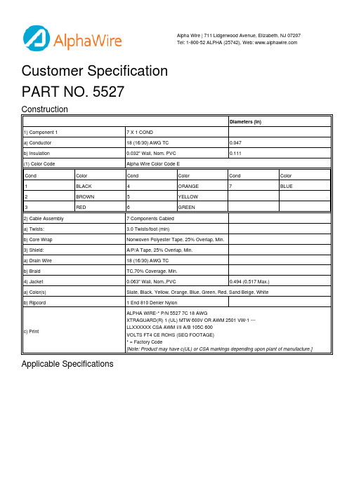
Alpha Wire | 711 Lidgerwood Avenue, Elizabeth, NJ 07207Tel: 1-800-52 ALPHA (25742), Web: Customer SpecificationPART NO. 5527ConstructionDiameters (In)1) Component 17 X 1 CONDa) Conductor18 (16/30) AWG TC0.047b) Insulation0.032" Wall, Nom. PVC0.111(1) Color Code Alpha Wire Color Code ECond Color Cond Color Cond Color1BLACK4ORANGE7BLUE2BROWN5YELLOW3RED6GREEN2) Cable Assembly7 Components Cableda) Twists: 3.0 Twists/foot (min)b) Core Wrap Nonwoven Polyester Tape, 25% Overlap, Min.3) Shield:A/P/A Tape, 25% Overlap, Min.a) Drain Wire18 (16/30) AWG TCb) Braid TC,70% Coverage, Min.4) Jacket0.063" Wall, Nom.,PVC0.494 (0.517 Max.)a) Color(s)Slate, Black, Yellow, Orange, Blue, Green, Red, Sand Beige, Whiteb) Ripcord 1 End 810 Denier Nylonc) Print ALPHA WIRE-* P/N 5527 7C 18 AWGXTRAGUARD(R) 1 (UL) MTW 600V OR AWM 2501 VW-1 ---LLXXXXXX CSA AWM I/II A/B 105C 600VOLTS FT4 CE ROHS (SEQ FOOTAGE)* = Factory Code[Note: Product may have c(UL) or CSA markings depending upon plant of manufacture.]Applicable Specifications1) ULa) Component 1AWM/STYLE 1015105°C / 600 V RMSMTW90°C Dry / 60°C Wet / 600 V RMSb) Overall MTW90°C Dry / 60°C Wet / 600 V RMSAWM/STYLE 2501105°C / 600 V RMSVW-12) CSA Internationala) Component 1TEW105°C / 600 V RMSb) Overall AWM I/II A/B105°C / 600 V RMSFT43) CE:EU Low Voltage Directive 2006/95/ECEnvironmental1) EU Directive 2002/95/EC(RoHS):All materials used in the manufacture of this part are in compliance with EU Directive2002/95/EU regarding the restriction of use of certain hazardous substances in electrical andelectronic equipment. Consult Alpha Wire's web site for compliance Date of Manufacture.2) REACH Regulation (EC 1907/2006):This product does not contain Substances of Very High Concern (SVHC) listed on the EuropeanUnion's REACH candidate list in excess of 0.1% mass of the item. For up-to-date information,please see Alpha's REACH SVHC Declaration.3) California Proposition 65:The outer surface materials used in the manufacture of this part meet the requirements of California Proposition 65.PropertiesPhysical & Mechanical Properties1) Temperature Range-30 to 105°C2) Bend Radius10X Cable Diameter3) Pull Tension107 Lbs, Maximum4) Sunlight Resistance YesElectrical Properties(For Engineering purposes only)1) Voltage Rating600 V RMS2) Capacitance36 pf/ft @1 kHz, Nominal Conductor to Conductor3) Ground Capacitance65 pf/ft @1 kHz, Nominal4) Inductance0.22 µH/ft, Nominal5) Conductor DCR7.2 /1000ft @20°C, Nominal6) OA Shield DCR 2.05 /1000ft @20°C, NominalOtherPackaging Flange x Traverse x Barrel (inches)a) 1000 FT24 x 14 x 12 Continuous lengthb) 500 FT18 x 12 x 8 Continuous lengthc) 100 FT16 x 11 x 8 Continuous lengthd) Bulk(Made-to-order)[Spool dimensions may vary slightly]Alpha Wire | 711 Lidgerwood Avenue, Elizabeth, NJ 07207Tel: 1-800-52 ALPHA (25742)Although Alpha Wire (“Alpha”) makes every reasonable effort to ensure there accuracy at the time of publication, information and specifications described herein are subject to errors or omissions and to changes without notice, and the listing of such information and specifications does not ensure product availability.Alpha provides the information and specifications herein on an “AS IS” basis, with no representations or warranties, whether express, statutory or implied. In no event will Alpha be liable for any damages (including consequential, indirect, incidental, special, punitive, or exemplary) whatsoever, even if Alpha had been advised of the possibility of such damages, whether in an action under contract, negligence or any other theory, arising out of or in connection with the use, or inability to use, the information or specifications described herein.Alpha Wire | 711 Lidgerwood Avenue, Elizabeth, NJ 07207Tel: 1-800-52 ALPHA (25742), Web: RoHS CERTIFICATE OF COMPLIANCETo Whom It May Concern:Alpha Wire Part Number:55275527 , RoHS-Compliant Commencing With8/1/2005ProductionThis document certifies that the Alpha part numbers cited above are manufactured in accordancewith Directive 2002/95/EC of the European Parliament and of the Council of 27 January 2003,better known as the RoHS Directives, with regards to restrictions of the use of certain hazardoussubstances used in the manufacture of electrical and electronic equipment. The reader is referredto these Directives for the specific definitions and extents of these Directives. No Exemptions arerequired for RoHS Compliance on this item.Substance Maximum Control ValueLead0.1% by weight (1000 ppm)Mercury0.1% by weight (1000 ppm)Cadmium0.01% by weight (100 ppm)Hexavalent Chromium0.1% by weight (1000 ppm)Polybrominated Biphenyls (PBB)0.1% by weight (1000 ppm)Polybrominated Diphenyl Ethers (PBDE)Including Deca-BDE0.1% by weight (1000 ppm)The information provided in this document and disclosure is correct to the best of Alpha Wire'sknowledge, information and belief at the date of its release. The information provided is designedonly as a general guide for the safe handling, storage, and any other operation of the productitself or the one that it will become part of. The intent of this document is not to be considered awarranty or quality specification. Regulatory information is for guidance purposes only. Productusers are responsible for determining the applicability of legislation and regulations based ontheir individual usage of the product.Authorized Signatory for the Alpha Wire Company:Dave Watson, Director of Engineering & QA11/1/2012。
7314中文资料

®
TDA7314
DIGITAL CONTROLLED AUDIO PROCESSOR WITH LOUDNESS
1 STEREO INPUT SELECTABLE INPUT GAIN FOR OPTIMAL ADAPTION TO DIFFERENT SOURCES INPUT AND OUTPUT FOR EXTERNAL EQUALIZER OR NOISE REDUCTION SYSTEM LOUDNESS FUNCTION VOLUME CONTROL IN 1.25dB STEPS TREBLE AND BASS CONTROL FOUR SPEAKER ATTENUATORS: - 4 INDEPENDENT SPEAKERS CONTROL IN 1.25dB STEPS FOR BALANCE AND FADER FACILITIES - INDEPENDENT MUTE FUNCTION ALL FUNCTIONS PROGRAMMABLE VIA SERIAL BUS DESCRIPTION The TDA7314 is a volume, tone (bass and treble) balance (Left/Right) and fader (front/rear) processor for quality audio applications in car radio and Hi-Fi systems. PIN CONNECTION (Top view)
AUDIO OUTPUTS
VOCL RL CL ROUT VOUT Clipping Level Output Load Resistance Output Load Capacitance Output resistance DC Voltage Level 30 4.2 75 4.5 d = 0.3% 2 2 10 120 4.8 2.5 Vrms KΩ nF Ω V
AT-41411中文资料
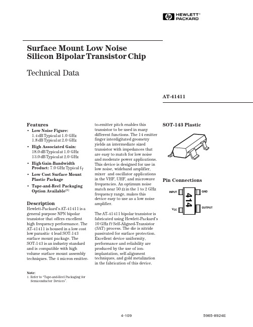
Surface Mount Low NoiseSilicon␣Bipolar Transistor Chip Technical DataFeatures•Low Noise Figure:1.4 dB Typical at 1.0␣GHz 1.8 dB Typical at 2.0␣GHz •High Associated Gain:18.0 dB Typical at 1.0␣GHz 13.0 dB Typical at 2.0␣GHz •High Gain-BandwidthProduct: 7.0 GHz Typical f T •Low Cost Surface Mount Plastic Package •Tape-and-Reel Packaging Option Available [1]AT-41411SOT-143 PlasticNote:1. Refer to “Tape-and-Reel Packaging forSemiconductor Devices”.DescriptionHewlett-Packard’s AT-41411 is a general purpose NPN bipolar transistor that offers excellent high frequency performance. The AT-41411 is housed in a low cost low parasitic 4 lead SOT-143surface mount package. The SOT-143 is an industry standard and is compatible with highvolume surface mount assembly techniques. The 4 micron emitter-to-emitter pitch enables this transistor to be used in manydifferent functions. The 14 emitter finger interdigitated geometry yields an intermediate sized transistor with impedances that are easy to match for low noise and moderate power applications.This device is designed for use in low noise, wideband amplifier,mixer and oscillator applications in the VHF, UHF, and microwave frequencies. An optimum noise match near 50 Ω in the 1 to 2 GHz frequency range, makes thisdevice easy to use as a low noise amplifier.The AT-41411 bipolar transistor is fabricated using Hewlett-Packard’s 10 GHz f T Self-Aligned-Transistor (SAT) process. The die is nitride passivated for surface protection.Excellent device uniformity,performance and reliability are produced by the use of ion-implantation, self-alignmenttechniques, and gold metalization in the fabrication of this device.Pin ConnectionsGNDOUTPUTINPUTV CCAT-41411 Absolute Maximum RatingsAbsolute Symbol Parameter Units Maximum[1] V EBO Emitter-Base Voltage V 1.5V CBO Collector-Base Voltage V20V CEO Collector-Emitter Voltage V12I C Collector Current mA50P T Power Dissipation[2,3]mW225T j Junction Temperature°C150T STG Storage Temperature°C-65 to 150Thermal Resistance[2,4]:θjc = 550°C/WNotes:1.Permanent damage may occur ifany of these limits are exceeded.2.T CASE= 25°C.3.Derate at 1.8 mW/°C for T C > 26°C.4.See MEASUREMENTS section“Thermal Resistance” for moreinformation.Part Number Ordering InformationPart Number Increment CommentsAT-41411-TR13000ReelAT-41411-BLK100BulkNote:For more information, see “Tape and Reel Packaging for Semiconductor Devices”.Electrical Specifications, T A = 25°CSymbol Parameters and Test Conditions[1]Units Min.Typ. Max. |S21E|2Insertion Power Gain; V CE = 8 V, I C = 20 mA f = 1.0 GHz dB14.516.5f = 2.0 GHz11.0P1 dB Power Output @ 1 dB Gain Compression f = 2.0 GHz dBm17.0 V CE = 8 V, I C = 20 mAG1 dB 1 dB Compressed Gain; V CE = 8 V, I C = 20 mA f = 2.0 GHz dB13.0NF O Optimum Noise Figure: V CE = 8 V, I C = 10 mA f = 1.0 GHz dB 1.4f = 2.0 GHz 1.8f = 4.0 GHz 3.5G A Gain @ NF O; V CE = 8 V, I C = 10 mA f = 1.0 GHz dB18.0f = 2.0 GHz13.0f = 4.0 GHz9.0f T Gain Bandwidth Product: V CE = 8 V, I C = 20 mA GHz7.0h FE Forward Current Transfer Ratio; V CE = 8 V, I C = 10 mA—30150270 I CBO Collector Cutoff Current; V CB = 8 VµA0.2 I EBO Emitter Cutoff Current; V EB = 1 VµA 1.0Notes:1.Refer to PACKAGING Section, “Tape-and-Reel Packaging for Semiconductor Devices.”AT-41411 Typical Performance, T A = 25°CFREQUENCY (GHz)G A I N (d B )I C (mA)Figure 2. Optimum Noise Figure and Associated Gain vs. Collector Current and Frequency. V CE = 8 V, f = 2.0 GHz.Figure 1. Noise Figure and Associated Gain vs. Frequency. V CE = 8 V, I C =10mA.G A IN(d B )0102030FREQUENCY (GHz)Figure 4. Insertion Power Gain, Maximum Available Gain andMaximum Stable Gain vs. Frequency. V CE = 8 V, I C = 20 mA.G A I N (d B )0.10.50.3 1.03.06.02421181512963042N F O (d B )420N F O (d B )0.52.01.0 3.0 4.016141210G AG A NF ONF OI C (mA)Figure 3. Insertion Power Gain vs. Collector Current and Frequency. V CE = 8 V.20161284|S 21E |2 G A I N (d B )01020304035302520151050AT-41411 Typical Scattering Parameters,Common Emitter, Z O = 50 Ω, T A=25°C, V CE=8V,I C␣=␣10 mAFreq.S11S21S12S22 GHz Mag.Ang.dB Mag.Ang.dB Mag.Ang.Mag.Ang.0.1.85-3027.323.20158-37.7.01364.93-110.5.58-11221.712.18109-29.1.03544.62-301.0.49-15616.5 6.7085-27.2.04443.50-331.5.4917813.2 4.5871-25.0.05647.46-362.0.5016010.83.4559-23.4.06847.45-412.5.531539.0 2.8253-22.5.07556.43-433.0.551427.5 2.3743-21.0.08954.43-533.5.56133 6.1 2.0233-19.8.10252.44-634.0.56121 4.9 1.7623-18.8.11549.46-73 AT-41411 Typical Scattering Parameters,Common Emitter, Z O = 50 Ω, T A=25°C, V CE=8V,I C␣=␣20 mAFreq.S11S21S12S22 GHz Mag.Ang.dB Mag.Ang.dB Mag.Ang.Mag.Ang.0.1.65-4630.433.07150-40.0.01059.89-150.5.46-13722.413.21100-32.0.02556.57-261.0.43-17516.7 6.8580-28.4.03858.52-291.5.4416313.3 4.6367-26.4.04861.51-322.0.4714810.83.4756-24.2.06261.50-372.5.501409.0 2.8250-22.9.07160.47-393.0.531327.5 2.3640-20.7.09261.46-483.5.55122 6.1 2.0230-19.6.10557.45-604.0.56112 4.8 1.7419-18.3.12253.45-73A model for this device is available in the DEVICE MODELS section.AT-41411 Noise Parameters: V CE = 8 V, I C = 10 mAFreq.NF OΓoptGHz dB Mag Ang R N/500.1 1.3.1240.170.5 1.3.10230.171.0 1.4.07570.162.0 1.8.09-1580.164.0 3.5.31-870.38SOT-143 Plastic DimensionsDIMENSIONS ARE IN MILLIMETERS (INCHES)TOP VIEW END VIEWSIDE VIEW。
西门子S1131消防产品手册
选配(最大配置):
BCH1935 双琴台
(1)
1个
Rack/WG 立柜(带玻璃门)
(1)
1个
ZA2711B/24 火警通讯盘
1个
ZA2711B/40 火警通讯盘
*
1个
ZA5711A 总线制火警通讯盘
*
1个
ZA2715/10 电话主机
*
1个
ZA2715/30 电话主机
*
1个
ZA2721A 广播录放盘
*
设备外观
3
S1131 产品手册
类型
功能描述 / 技术参数
部件号
FS1120
FS1120 CC114x-/A/Rack 分布式系统控制器 (上柜式)
CC114x-/A/Rack (瑞士部件,中国组装)
● 适用 S1131 分布式系统。 ● 设计容量:2000 点。 ● 标准 H67 安装底板组件,可安装于 BCH1950 双琴台或 Rack/WG
AC220V,± 15%,50/60Hz DC24V,38AH 0 ~ 50℃ - 20 ~ 60℃ ≤ 95%(40 ± 2℃) IP30 RAL 7035 淡灰色 434 X 1130 X 300 (mm)
基本配置:
CC1142 主 CPU 控制单元
1个
CT1142 控制面板终端
1个
E3M111 回路卡(4 回路) B2F020 电源(DC29V/6A)
基本配置:
BCH1950 双琴台
(1)
1个
CC1142 主 CPU 控制单元
1个
E3M111 回路卡(4 回路)
*
1块
B2F020 电源(DC29V/6A)
电脑显卡视频双显示器输出全攻略
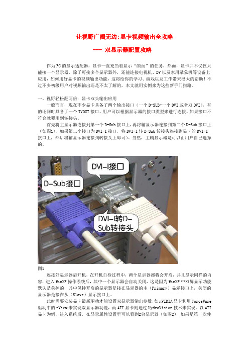
让视野广阔无边:显卡视频输出全攻略--- 双显示器配置攻略作为PC的显示适配器,显卡一直充当着显示“颜面”的任务,然而,显卡并不仅仅只能接一个显示器,除了可接多个显示器外,还能连接电视机、DV以及家用录象机等设备上应用,如何用好显卡的视频输出功能,这将给你的学习、游戏以及工作带来很大的帮助!不过不少初级用户对视频输出还是不太了解的,本文就用实例来为这些新手门指路。
一、视野轻松翻两倍:显卡双头输出应用一般而言,现在不少显卡具备了两个输出接口(一个D-SUB+一个DVI或者双DVI),有的还同时具备了一个TVOUT接口。
用户可以根据显示器的接口类型来进行连接。
如果接口不符合就要用到转接头。
首先将主显示器连接到第一个D-Sub接口上,再将辅显示器连接到第二个D-Sub接口上(如图1),如果第二个接口为DVI-I接口,将DVI-I转D-Sub转接头连接到显卡的DVI-I 接口上,然后将辅显示器连接到转接头上即可)。
当然,主辅显示器是可以由用户自己选择的。
图1连接好显示器后开机,在开机自检过程中,两个显示器都将会开启,并且显示同样的内容,进入WinXP操作系统后,其中一个显示器会自动关闭,这是因为WinXP中双屏显示功能默认是关掉的,其中保持开启的显示器是接在显示器的主(Primary)显示接口上,关闭的显示器是接在从(Slave)显示接口上。
此时需要安装显卡最新驱动才能设置双显示器输出参数,如nVIDIA显卡利用ForceWare 驱动中的nView来实现双显示器功能,而ATI显卡则通过HydraVision技术来实现。
以ATI 显卡为例,进入系统后,在显示属性设置里可以看到2台显示器(如图2),如果是第一次使用,第2台显示器是灰色的,表示没有启用。
双击第2台显示器,系统会弹出对话框,询问是否启用显示器。
图2选择“是”之后,第二台显示器就会正确的显示扩展的WINDWOS桌面。
点击“高级”—“显示”进入显示设备设置窗口(如图3)。
BA3314中文资料

217
元器件交易网 Audio ICs
FAbsolute maximum ratings (Ta = 25_C)
BA3314F
FRecommended operating conditions (Ta = 25_C)
FElectrical characteristics (unless otherwise noted, Ta = 25_C, VCC = 8V and f= 1kHz)
219
元器件交易网 Audio ICs
FApplication example
BA3314F
FElectrical characteristics curve
FExternal dimensions (Units: mm)
220
218
元器件交易网 Audio ICs
FMeasurement circuit
FOperation notes Changing the input resistor R g , and the ALC time constant influences the ALC transient characteristics. In particular, if Rg is less than 3.9kΩ or the time constant capacitor is less than 47µF, the ALC may operate excessively. Do not use smaller values than those recommended for these components.
元器件交易网 Audio ICs
Dual preamplifier with ALC detector circuit
(整理)彩色液晶屏接口及其驱动电路
(整理)彩色液晶屏接口及其驱动电路彩色液晶屏接口及其驱动电路市场上有大批的各种型号的液晶屏,广大用户及电子爱好者都想利用二手屏开发液晶电视或制作投影机,但目前有关这方面的资料和书籍比较少,很多人拿到液晶屏却找不到相关资料,而束手无策。
本人从事彩色液晶行业多年,愿将相关资料和经验与广大电子爱好者共享。
一、市场流行二手屏简介目前市场上主要是STN 型彩色液晶屏(俗称伪彩屏)和TFT 型彩色液晶屏(俗称真彩屏)。
从接口方式上分有数字屏和模拟屏。
目前在我国市场上电子爱好者通常能买到的大部分是二手屏,一般以日本公司的产品为主,品种很多。
但由于此类液晶屏大都为日本的PACHINKO (俗称柏青哥,一种小钢珠的赌博游戏)机的拆机屏。
由于此类屏数量多,价格便宜,市场拥有量大,所以本文重点介绍此类液晶屏的接口及其驱动电路。
日本PACHINKO(柏青哥)游戏机用液晶屏一览表如附表所示。
需说明的是:关于液晶屏的图象分辨率,许多厂家的标注方法不同,象320×234,有的液晶屏资料上标注为960×234,这实际上是将R、G、B 三基色乘上了320。
即3×320=960。
同样地,7" 16:9 的屏有的标为480×234,有的标为1440×234,它也是将3×480=1440 而得出的。
图象的分辨率指标主要是看垂直方向的线数,比如,两个分别标有800×480 和1440×234的7"液晶屏,哪个像素点多,分辨率高呢?显然应该是800×480的分辨率高,它是数字屏,可以支持VGA输入。
那么是不是数字屏就分辨率高呢?也不尽然。
象附表中的夏普LM32C041,EPSON 4"、 5.6"、 6.5",ALPS LFUBK9111A/LFUBK3041A 虽然是数字屏,但其分辨率也只有320×234。
- 1、下载文档前请自行甄别文档内容的完整性,平台不提供额外的编辑、内容补充、找答案等附加服务。
- 2、"仅部分预览"的文档,不可在线预览部分如存在完整性等问题,可反馈申请退款(可完整预览的文档不适用该条件!)。
- 3、如文档侵犯您的权益,请联系客服反馈,我们会尽快为您处理(人工客服工作时间:9:00-18:30)。
2000 Mar 15
2
元器件交易网
Philips Semiconductors
Preliminary specification
PAL/NTSC/SECAM video decoder with adaptive PAL/NTSC comb filter, VBI-data slicer and high performance scaler
Preliminary specification File under Integrated Circuits, IC22 2000 Mar 15
元器件交易网
Philips Semiconductors
Preliminary specification
PAL/NTSC/SECAM video decoder with adaptive PAL/NTSC SAA7114H comb filter, VBI-data slicer and high performance scaler
• Versatile VBI-data decoder, slicer, clock regeneration and byte synchronization e.g. for World Standard Teletext (WST), North-American Broadcast Text System (NABTS), close caption, Wide Screen Signalling (WSS) etc. 1.4 Audio clock generation
CONTENTS 1 1.1 1.2 1.3 1.4 1.5 1.6 2 3 4 5 6 7 8 8.1 8.2 8.3 8.4 8.5 8.6 9 9.1 9.2 9.3 9.4 9.5 9.6 9.7 FEATURES Video decoder Video scaler Vertical Blanking Interval (VBI) data decoder and slicer Audio clock generation Digital I/O interfaces Miscellaneous APPLICATIONS GENERAL DESCRIPTION QUICK REFERENCE DATA ORDERING INFORMATION BLOCK DIAGRAM PINNING FUNCTIONAL DESCRIPTION Decoder Decoder output formatter Scaler VBI-data decoder and capture (subaddresses 40H to 7FH) Image port output formatter (subaddresses 84H to 87H) Audio clock generation (subaddresses 30H to 3FH) INPUT/OUTPUT INTERFACES AND PORTS Analog terminals Audio clock signals Clock and real-time synchronization signals Video expansion port (X-port) Image port (I-port) Host port for 16-bit extension of video data I/O (H-port) Basic input and output timing diagrams I-port and X-port 16 16.1 16.2 16.3 16.4 17 18 18.1 18.2 18.3 18.4 18.5 19 20 21 10 10.1 10.2 11 12 13 14 15 15.1 15.2 15.3 15.4 15.5 BOUNDARY SCAN TEST Initialization of boundary scan circuit Device identification codes LIMITING VALUES THERMAL CHARACTERISTICS CHARACTERISTICS APPLICATION INFORMATION I2C-BUS DESCRIPTION I2C-bus format I2C-bus details Programming register audio clock generation Programming register VBI-data slicer Programming register interfaces and scaler part PROGRAMMING START SET-UP Decoder part Audio clock generation part Data slicer and data type control part Scaler and interfaces PACKAGE OUTLINE SOLDERING Introduction to soldering surface mount packages Reflow soldering Wave soldering Manual soldering Suitability of surface mount IC packages for wave and reflow soldering methods DEFINITIONS LIFE SUPPORT APPLICATIONS PURCHASE OF PHILIPS I2C COMPONENTS
1 1.1 FEATURES Video decoder
SAA7114H
• Six analog inputs, internal analog source selectors, e.g. 6 × CVBS or (2 × Y/C and 2 × CVBS) or (1 × Y/C and 4 × CVBS) • Two analog preprocessing channels in differential CMOS style inclusive built-in analog anti-alias filters • Fully programmable static gain or Automatic Gain Control (AGC) for the selected CVBS or Y/C channel • Automatic Clamp Control (ACC) for CVBS, Y and C • Switchable white peak control • Two 9-bit video CMOS Analog-to-Digital Converters (ADCs), digitized CVBS or Y/C signals are available on the expansion port • On-chip line-locked clock generation according “ITU 601” • Digital PLL for synchronization and clock generation from all standards and non-standard video sources e.g. consumer grade VTR • Requires only one crystal (32.11 or 24.576 MHz) for all standards • Horizontal and vertical sync detection • Automatic detection of 50 and 60 Hz field frequency, and automatic switching between PAL and NTSC standards • Luminance and chrominance signal processing for PAL BGDHIN, combination PAL N, PAL M, NTSC M, NTSC-Japan, NTSC 4.43 and SECAM • Adaptive 2/4-line comb filter for two dimensional chrominance/luminance separation – Increased luminance and chrominance bandwidth for all PAL and NTSC standards – Reduced cross colour and cross luminance artefacts • PAL delay line for correcting PAL phase errors • Independent Brightness Contrast Saturation (BCS) adjustment for decoder part • User programmable sharpness control • Independent gain and offset adjustment for raw data path. 1.2 Video scaler
元器件交易网
ห้องสมุดไป่ตู้
INTEGRATED CIRCUITS
DATA SHEET
SAA7114H PAL/NTSC/SECAM video decoder with adaptive PAL/NTSC comb filter, VBI-data slicer and high performance scaler
• Horizontal and vertical down-scaling and up-scaling to randomly sized windows • Horizontal and vertical scaling range: variable zoom to 1⁄ (icon); it should be noted that the H and V zoom are 64 restricted by the transfer data rates • Anti-alias and accumulating filter for horizontal scaling • Vertical scaling with linear phase interpolation and accumulating filter for anti-aliasing (6-bit phase accuracy) • Horizontal phase correct up and down scaling for improved signal quality of scaled data, especially for compression and video phone applications, with 6-bit phase accuracy (1.2 ns step width) • Two independent programming sets for scaler part, to define two ‘ranges’ per field or sequences over frames • Fieldwise switching between decoder part and expansion port (X-port) input • Brightness, contrast and saturation controls for scaled outputs. 1.3 Vertical Blanking Interval (VBI) data decoder and slicer
