Contact and Interconnection
国际备用证惯例ISP98(英文)

INTERNATIONAL STANDBY PRACTICES (ISP98) ForewordPROLOGUEby Dr. Gerold Herrmann, Secretary, United Nations Commission on International Trade Law (UNCITRAL)It was an extremely interesting and enriching experience for me to assist in drafting ISP98. This participation allowed me to witness (and now bear witness to) the very thorough and pragmatic drafting process in a superbly selected group, with representatives of all interested sectors actively involved in standby letter of credit practice such as: bankers, especially those responsible for letter of credit operations and global trade transactions, bank counsel, attorneys, academics, regulators, government officials, corporate treasurers, and likely influential beneficiaries. The treasure trove of experience and expertise and the diversity of interests and perspectives proved invaluable in determining- as was continuously done by examining concrete practical examples- whether on a given issue an operational rule would be desirable and useful and, if so, which solution would work best and reflect good practice.Continued participation in the preparatory work has also convinced me- as, I am sure, it would have anyone else- of the special characteristics of standbys at the operational level of practical detail and usage. Their special features, in my view, not only justify but also necessitate special contractual rules designed for standbys. As the constant comparison with the UCP clearly revealed, quite a few UCP Articles are inappropriate for standbys and quite a few issues of paramount importance in standby practice are not addressed at all in the UCP. While a similar disparity in practice exists between the standby and the independent guarantee (the bank or demand guarantee European style), this seems particularly, if not exclusively, true for those types of actual use (e.g. financial standby, direct-pay standby) hitherto found only extremely rarely in guarantee practice. For this and other reasons, including firmness of the undertaking, I would not be surprised to see not only standbys but also some demand guarantees issued subject to ISP98.For a professional unifier of law, participation in the preparatory work was particularly satisfying because of its interconnection with other harmonisation and reform efforts. In addition to the concordance with revised Article 5 UCC (the letter-of-credit law of the homeland of the standby) and the similarly close contact (and personal overlap) with the 1993 UCP revision task force, I am referring in particular to UNCITRAL's work which culminated in the adoption in 1995 by the General Assembly of the "United Nations Convention on Independent Guarantees and Stand-by Letters of Credit." The idea of preparing special operational rules for standbys was born during the extensive debates comparing national laws as well as the two instruments to be married by that Convention. Since bride and groom were presented there in all facets and critically scrutinized by their future in-laws, UNCITRAL's travaux preparatoires make for highly informative reading (as will future abstracts of court decisions to be published in UNCITRAL'scase collection system called CLOUT; homepage: www.un.or.at/uncitral). It was gratifying to see the group preparing ISP98 refer continuously to the UNCITRAL Convention in order to ensure complete consistency. I must admit to special gratification by overhearing one of the world's leading letter of credit expert's remark to his banking colleague: "The more I look at this UN Convention, the more I really like it."The above coordination or cooperation in the universal harmonisation and modernization efforts is welcome and in fact crucial because of the (often neglected or ignored) interdependence between the two very different levels of legal norms: the contractual level, where such sets of rules like ISP98, UCP 500, or URDG become effective by agreement of the individual parties, and the statutory level, where internationally elaborated law like the UN Convention or domestic law (e.g. Art. 5 UCC) recognise and give full effect to the exercise of that party autonomy and regulate certain issues that can effectively be settled only at that level (e.g. standards of fraud exception, injunctive relief and other court matters). Therefore, ISP98 and the Convention supplement each other in an ideal manner and together lay the necessary basis for a smooth functioning of standby practice worldwide.PrefaceThe International Standby Practices (ISP98) reflects generally accepted practice, custom, and usage of standby letters of credit. It provides separate rules for standby letters of credit in the same sense that the Uniform Customs and Practice for Documentary Credits (UCP) and the Uniform Rules for Demand Guarantees (URDG) do for commercial letters of credit and independent bank guarantees.The formulation of standby letter of credit practices in separate rules evidences the maturity and importance of this financial product. The amounts outstanding of standbys greatly exceed the outstanding amounts of commercial letters of credit. While the standby is associated with the United States where it originated and where it is most widely used, it is truly an international product. Non-U.S. bank outstandings have exceeded those of U.S. banks in the United States alone. Moreover, the standby is used increasingly throughout the world.For convenience, standbys are commonly classified descriptively (and without operative significance in the application of these Rules) based on their function in the underlying transaction or other factors not necessarily related to the terms and conditions of the standby itself. For example:ll A "Performance Standby" supports an obligation to perform other than to pay money including for the purpose of covering losses arising from a default of the applicant in completion of the underlying transactions.l An "Advance Payment Standby" supports an obligation to account for an advance payment made by the beneficiary to the applicant.l A "Bid Bond/Tender Bond Standby" supports an obligation of the applicant to execute a contract if the applicant is awarded a bid.l A "Counter Standby" supports the issuance of a separate standby or other undertaking by the beneficiary of the counter standby.l A "Financial Standby" supports an obligation to pay money, including any instrument evidencing an obligation to repay borrowed money.l A "Direct Pay Standby" supports payment when due of an underlying payment obligation typically in connection with a financial standby without regard to a default.l An "Insurance Standby" supports an insurance or reinsurance obligation of the applicant.l A "Commercial Standby" supports the obligations of an applicant to pay for goods or services in the event of non-payment by other methods.In the past, many standbys have been issued subject to the UCP even though it was intended for commercial letters of credit. The UCP reinforced the independence and documentary character of the standby. It also provided standards for examination and notice of dishonor and a basis to resist market pressures to embrace troublesome practices such as the issuance of standbys without expiration dates.Despite these important contributions, it has long been apparent that the UCP was not fully applicable nor appropriate for standbys, as is recognized in UCP 500 Article 1 which provides that it applies to the extent to which they may be applicable. Even the least complex standbys (those calling for presentation of a draft only) pose problems not addressed by the UCP. More complex standbys (those involving longer terms or automatic extensions, transfer on demand, requests that the beneficiary issue its own undertaking to another, and the like) require more specialized rules of practice. The ISP fills these needs.The ISP differs from the UCP in style and approach because it must receive acceptance not only from bankers and merchants, but also from a broader range of those actively involved in standby law and practice corporate treasurers and credit managers, rating agencies, government agencies and regulators, and indenture trustees as well as their counsel. Because standbys are often intended to be available in the event of disputes or applicant insolvency, their texts are subject to a degree of scrutiny not encountered in the commercial letter of credit context. As a result, the ISP is also written to provide guidance to lawyers and judges in the interpretation of standby practice.Differences in substance result either from different practices, different problems, or the need for more precision. In addition, the ISP proposes basic definitions should the standby permit or require presentation of documents by electronic means. Since standbys infrequently require presentation of negotiable documents, standby practice is currently more conducive to electronic presentations, and the ISP provides definitions and rules encouraging such presentations. The development of S.W.I.F.T. message types for the ISP is anticipated.The ISP, like the UCP for commercial letters of credit, simplifies, standardizes, and streamlines the drafting of standbys, and provides clear and widely accepted answers to common problems. There are basic similarities with the UCP because standby and commercial practices are fundamentally the same. Even where the rules overlap, however, the ISP is more precise, stating the intent implied in the UCP rule, in order to make the standby more dependable when a drawing or honor is questioned.Like the UCP and the URDG, the ISP will apply to any independent undertaking issued subject to it. This approach avoids the impractical and often impossible task of identifying and distinguishing standbys from independent guarantees and, in many cases, commercial letters of credit. The choice of which set of rules to select is, therefore, left to the parties as it should be. One may well choose to use the ISP for certain types of standbys, the UCP for others, and the URDG for still others. While the ISP is not intended to be used for dependent undertakings such as accessory guarantees and insurance contracts, it may be useful in some situations inindicating that a particular undertaking which might otherwise be treated as dependent under local law is intended to be independent.For the ISP to apply to a standby, an undertaking should be made subject to these Rules by including language such as (but not limited to):l This undertaking is issued subject to the International Standby Practices 1998.orl Subject to ISP98.Although the ISP can be varied by the text of a standby, it provides neutral rules acceptable in the majority of situations and a useful starting point for negotiations in other situations. It will save parties (including banks that issue, confirm, or are beneficiaries of standbys) considerable time and expense in negotiating and drafting standby terms.The ISP is designed to be compatible with the United Nations Convention on Independent Guarantees and Stand-by Letters of Credit (which represents a useful and practical formulation of basic standby and independent guarantee law) and also with local law, whether statutory or judicial, and to embody standby letter of credit practice under that law. If these rules conflict with mandatory law on issues such as assignment of proceeds or transfer by operation of law, applicable law will, of course, control. Nonetheless, most of these issues are rarely addressed by local law and progressive commercial law will often look to the practice as recorded in the ISP for guidance in such situations, especially with respect to cross border under-takings. As a result, it is expected that the ISP will complement local law rather than conflict with it.The ISP is intended to be used also in arbitration as well as judicial proceedings (such as the expert based letter of credit arbitration system developed by the International Center for Letter of Credit Arbitration (ICLOCA) Rules or general commercial ICC arbitration) or with alternative methods of dispute resolution. Such a choice should be made expressly and with appropriate detail. At a minimum, it can be made in connection with the clause relating to ISP98 - e.g. This undertaking is issued subject to ISP98, and all disputes arising out of it or related to it are subject to arbitration under ICLOCA Rules (1996).Although translations of the ISP into other languages are envisioned and will be monitored for integrity, the English text is the official text of the ISP in the event of disputes.The ISP is the product of the work of the ISP Working Group under the auspices of the Institute of International Banking Law and Practice, Inc. which interacted with hundreds of persons over a five year period, and has benefited from comments received from individuals, banks, and national and international associations. In particular, the participation of the International Financial Services Association (formerly the USCIB) and the Ad Hoc Working Group under the chairmanship of Gary Collyer (which led to its endorsement by the ICC Banking Commission) is gratefully recognized. In addition, the sponsorship and support of Citibank N.A., The Chase Manhattan Bank, ABN-AMRO, Baker and McKenzie, and the National Law Center for Inter-American Free Trade is acknowledged. Perhaps the greatest significance of the ISP is that its creation marks a new chapter in the collaboration between the international banking operations community and the legal community at an international level. In this respect, the active role played in this process by the Secretariat of the United Nations Commission on International Trade Law has been invaluable.The ISP is drafted as a set of rules intended for use in daily practice. It is not intended toprovide introductory information on standbys and their uses. While it is recognized that specific rules would benefit from explanatory comments, such comments are not appended to the ISP because the resulting work would be too cumbersome for daily use. Instead, introductory materials and Official Comments are available in the Official Commentary on the International Standby Practices (ISP98). For further information on support materials and developments on the ISP and to pose queries, consult the ISP98 website: .Professor James E. ByrneDirector, Institute of International Banking Law and Practice, Inc.; Chair and Reporter, P Working GroupJames G. BarnesBaker and McKenzie; Vice Chair, ISP Working GroupGary W. CollyerVice President, Citibank, N.A; Chair, ICC Ad Hoc Working Group and Technical Adviser to the ICC Banking Commission1. GENERAL PROVISIONSScope, Application, Definitions, and Interpretation of These Rules1.01 Scope and Applicationa. These Rules are intended to be applied to standby letters of credit (including performance, financial, and direct pay standby letter of credit)b. A standby letter of credit or other similar undertaking, however named or described, whether for domestic or international use, may be made subject to these Rules by express reference to them.c. An undertaking subject to these Rules may expressly modify or exclude their application.d. An undertaking subject to these Rules is hereinafter referred to as a "standby".1.02 Relationship to Law and Other Rulesa. These Rules supplement the applicable law to the extent not prohibited by that law.b. These Rules supersede conflicting provisions in any other rules of practice to which a standby letter of credit is also made subject.1.03 Interpretative PrinciplesThese Rules shall be interpreted as mercantile usage with regard for:a. integrity of standbys as reliable and efficient undertakings to payb. practice and terminology of banks and businesses in day-to-day transactionsc. consistency within the worldwide system of banking operations and commerce; andd. worldwide uniformity in their interpretation and application.。
PMP英文项目经验范文十一例(经过PMI协会认证)(可编辑)

PMP英文项目经验范文十一例(经过PMI协会认证)Building Professionalism in projectmanagement. TMProject Management InstituteGlobal Operations Center14 Campus Blvd., Newtown Square, PA 19073-3299 USATel: +610-356-4600, Fax: +610-356-4647E-mail:*************,Internet://0>.Project Management Experience Audit ReportPMI ID Number Reference Experience NumberLast Name, First NameOrganization NameContact Name Email Address Phone Number1Project TitleShandong telecom base station power environmental monitoring projectStart Date End Date07/2009 11/2009DomainsInitiating Planning Executing Controlling Closing89.00 77.00 58.00 82.00 59.00Project DescriptionProject Name: Shandong telecom base station power environmentalmonitoring projectTarget: Shandong Telecom wireless base station power for remotemonitoring and management environmentProject deliverables: 1700 base stations across the province toachieve the power and the environment all theparameters such as remote capture and remote control and management.The output of the project: program testing, technical proposals, theimplementation of the program, completionof the test report.Candidate: Page 1 of 3Building Professionalism in project management.TMProject Management InstituteGlobal Operations Center14 Campus Blvd., Newtown Square, PA 19073-3299 USATel: +610-356-4600, Fax: +610-356-4647E-mail:*************,Internet://.Project Management Experience Audit ReportPMI ID Number Reference Experience NumberLast Name, First NamePMP? Experience Verification FormThe PMI credentials are the most recognized credentials in project managementTo maintain and enhance the high standard ofthese credentials PMI must ensure that project management practitioners who apply for the PMI credential examinations meetthe predefined requirements for eligibility One way in which PMI works to ensure that all educational and experientialrequirements are met and the integrity of its credentials are maintained is to conduct candidate auditsThe applicant who has presented you with this form has been randomly selected to participate in this auditPlease verify the accuracy of thecandidate’s experience presented on the Project Management Experience Report by providing your signature and contact information in the spaces belowPlease place these forms in an envelope, seal and sign your name over the back flap andreturn it to the candidatePMI appreciates your assistance in preserving the value of our credentials.I hereby verify that the information provided is correct. orYes NoIf NO, please provide the reason; if additional space is needed, continue on the back of this page:Name:Title:Organization:Address:Phone Number: Email:SignatureCandidate: Page 2 of 3Building Professionalism in project management. TMProject Management InstituteGlobal Operations Center14 Campus Blvd., Newtown Square, PA 19073-3299 USATel: +610-356-4600, Fax: +610-356-4647E-mail:*************,Internet://.Project Management Experience Audit ReportPMI ID Number Reference Experience NumberLast Name, First NameIf you have any questions regarding the audit, please contact the Project Management Institute at:Project Management InstituteAtt: Certification Audit14 Campus Blvd.Newtown Square, PA 19073-3299 USA************************Candidate: 1622191 Page 3 of 3Building Professionalism in project management. TMProject Management InstituteGlobal Operations Center14 Campus Blvd., Newtown Square, PA 19073-3299 USATel: +610-356-4600, Fax: +610-356-4647E-mail:*************,Internet://.Project Management Experience Audit ReportPMI ID Number Reference Experience NumberLast Name, First NameOrganization NameContact Name Email Address Phone Number1Project TitleShandong Commercial Group WAN ProjectStart Date End Date11/2007 03/2008DomainsInitiating Planning Executing Controlling Closing204.00 254.00 240.00 72.00 144.00Project DescriptionProject Name: Shandong Business Group WAN interconnection project Objectives: Group under the various industries and business systemsin real time based data processingbusiness.Project deliverables: Division by 52 nationwide green way to access groups through the headquarters, to meetthe retail, real estate, newspapers, car trade, logistics, educationand other daily operations of the industry.The output of the project: project planning, technical proposals, implementation plans, test reports and deviceconfiguration documentationCandidate: Page 1 of 3Building Professionalism in project management. TMProject Management InstituteGlobal Operations Center14 Campus Blvd., Newtown Square, PA 19073-3299 USATel: +610-356-4600, Fax: +610-356-4647E-mail:*************,Internet://.Project Management Experience Audit ReportPMI ID Number Reference Experience NumberLast Name, First NamePMP? Experience Verification FormThe PMI credentials are the most recognized credentials in project managementTo maintain and enhance the high standard ofthese credentials PMI must ensure that project management practitioners who apply for the PMI credential examinations meetthe predefined requirements for eligibility One way in which PMI works to ensure that all educational and experientialrequirements are met and the integrity of its credentials are maintained is to conduct candidate auditsThe applicant who has presented you with this form has been randomly selected to participate in this auditPlease verify the accuracy of thecandida te’s experience presented on the Project Management Experience Report by providing your signature and contact information in the spaces belowPlease place these forms in an envelope, seal and sign your name over the back flap andreturn it to the candidatePMI appreciates your assistance in preserving the value of our credentials.I hereby verify that the information provided is correct. orYes NoIf NO, please provide the reason; if additional space is needed, continue on the back of this page:Name:Title:Organization:Address:Phone Number: Email:SignatureCandidate: Page 2 of 3Building Professionalism in project management. TMProject Management InstituteGlobal Operations Center14 Campus Blvd., Newtown Square, PA 19073-3299 USATel: +610-356-4600, Fax: +610-356-4647E-mail:*************,Internet://.Project Management Experience Audit ReportPMI ID Number Reference Experience NumberLast Name, First NameIf you have any questions regarding the audit, please contact the Project Management Institute at:Project Management InstituteAtt: Certification Audit14 Campus Blvd.Newtown Square, PA 19073-3299 USA************************Candidate: Page 3 of 3Building Professionalism in project management.TMProject Management InstituteGlobal Operations Center14 Campus Blvd., Newtown Square, PA 19073-3299 USATel: +610-356-4600, Fax: +610-356-4647E-mail:*************,Internet://.Project Management Experience Audit ReportPMI ID Number Reference Experience NumberLast Name, First NameOrganization NameContact Name Email Address Phone Number1Project TitleShenzhen Airlines Jinan Branch information technology projectStart Date End Date04/2007 06/2007DomainsInitiating Planning Executing Controlling Closing130.00 174.00 178.00 50.00 122.00Project DescriptionProject Name: Shenzhen Airlines Jinan Branch information technology projectsGoal: data sharing and interoperability with HeadquartersProject deliverables: The new office building cabling, deployment, floor access and aggregation switches,firewalls deployed in exports, to ensure authorized access and external network data isolation.The output of the project: technical proposals, the implementationof the program, completion of the testreport.Candidate: Page 1 of 3Building Professionalism in project management. TMProject Management InstituteGlobal Operations Center14 Campus Blvd., Newtown Square, PA 19073-3299 USATel: +610-356-4600, Fax: +610-356-4647E-mail:*************,Internet://.Project Management Experience Audit ReportPMI ID Number Reference Experience NumberLast Name, First NamePMP? Experience Verification FormThe PMI credentials are the most recognized credentials in project managementTo maintain and enhance the high standard ofthese credentials PMI must ensure that project managementpractitioners who apply for the PMI credential examinations meetthe predefined requirements for eligibility One way in which PMI works to ensure that all educational and experientialrequirements are met and the integrity of its credentials are maintained is to conduct candidate auditsThe applicant who has presented you with this form has been randomly selected to participate in this auditPlease verify the accuracy of thecandidate’s experience presented on the Project Management Experience Report by providing your signature and contact information in the spaces belowPlease place these forms in an envelope, seal and sign your name over the back flap andreturn it to the candidatePMI appreciates your assistance in preserving the value of our credentials.I hereby verify that the information provided is correct. orYes NoIf NO, please provide the reason; if additional space is needed, continue on the back of this page:Name:Title:Organization:Address:Phone Number: Email:SignatureCandidate: Page 2 of 3Building Professionalism in project management. TMProject Management InstituteGlobal Operations Center14 Campus Blvd., Newtown Square, PA 19073-3299 USATel: +610-356-4600, Fax: +610-356-4647E-mail:*************,Internet://.Project Management Experience Audit ReportPMI ID Number Reference Experience NumberLast Name, First NameIf you have any questions regarding the audit, please contact the Project Management Institute at:Project Management InstituteAtt: Certification Audit14 Campus Blvd.Newtown Square, PA 19073-3299 USA************************Candidate: Page 3 of 3Building Professionalism in project management. TMProject Management InstituteGlobal Operations Center14 Campus Blvd., Newtown Square, PA 19073-3299 USATel: +610-356-4600, Fax: +610-356-4647E-mail:*************,Internet://.Project Management Experience Audit ReportPMI ID Number Reference Experience NumberLast Name, First NameOrganization NameContact Name Email Address Phone Number1Project TitleChina Ministry of Information System Project Phase II Shandong node Start Date End Date01/2006 02/2006DomainsInitiating Planning Executing Controlling Closing56.00 85.00 72.00 38.00 50.00Project DescriptionProject Name: Ministry of Public Security, Shandong secondary network nodesGoal: Wide Area Network expansion and backup routesProject deliverables: router card replacement 155M, and open to Beijing and Shanghai, two 155M circuit, thenode with the Ministry of Public Security a bidirectional high-speed communications.The output of the project: implementation of the program, completion of the test report.Candidate: Page 1 of 3Building Professionalism in project management. TMProject Management InstituteGlobal Operations Center14 Campus Blvd., Newtown Square, PA 19073-3299 USATel: +610-356-4600, Fax: +610-356-4647E-mail:*************,Internet://.Project Management Experience Audit ReportPMI ID Number Reference Experience NumberLast Name, First NamePMP? Experience Verification FormThe PMI credentials are the most recognized credentials in project managementTo maintain and enhance the high standard ofthese credentials PMI must ensure that project management practitioners who apply for the PMI credential examinations meet the predefined requirements for eligibility One way in which PMI works to ensure that all educational and experientialrequirements are met and the integrity of its credentials aremaintained is to conduct candidate auditsThe applicant who has presented you with this form has been randomly selected to participate in this auditPlease verify the accuracy of thecandidate’s experience presented on the Project Management Experience Report by providing your signature and contact information in the spaces belowPlease place these forms in an envelope, seal and sign your name over the back flap andreturn it to the candidatePMI appreciates your assistance in preserving the value of our credentials.I hereby verify that the information provided is correct. orYes NoIf NO, please provide the reason; if additional space is needed, continue on the back of this page:Name:Title:Organization:Address:Phone Number: Email:SignatureCandidate: Page 2 of 3Building Professionalism in project management. TMProject Management InstituteGlobal Operations Center14 Campus Blvd., Newtown Square, PA 19073-3299 USATel: +610-356-4600, Fax: +610-356-4647E-mail:*************,Internet://.Project Management Experience Audit ReportPMI ID Number Reference Experience NumberLast Name, First NameIf you have any questions regarding the audit, please contact the Project Management Institute at:Project Management InstituteAtt: Certification Audit14 Campus Blvd.Newtown Square, PA 19073-3299 USA************************Candidate: Page 3 of 3Building Professionalism in project management. TMProject Management InstituteGlobal Operations Center14 Campus Blvd., Newtown Square, PA 19073-3299 USATel: +610-356-4600, Fax: +610-356-4647E-mail:*************,Internet://.Project Management Experience Audit ReportPMI ID Number Reference Experience NumberLast Name, First NameOrganization NameContact Name Email Address Phone Number1Project TitleState Taxation Bureau of Shandong Province WAN transformation project Start Date End Date03/2005 06/2005DomainsInitiating Planning Executing Controlling Closing78.00 70.00 71.00 44.00 48.00Project DescriptionProject Name: Shandong Province, State Administration of Taxation network speed projectGoal: Wide Area Network expansion and backup routesProject deliverables: the provincial bureau to PUC to 17 speed wide area network by the 2M to 10M dual-routeback up, 3 years to meet the business tax system in Shandong data channel is not congested.The output of the project: technical proposals, the implementationof the program, completion of the testreport.Candidate: Page 1 of 3Building Professionalism in project management. TMProject Management InstituteGlobal Operations Center14 Campus Blvd., Newtown Square, PA 19073-3299 USATel: +610-356-4600, Fax: +610-356-4647E-mail:*************,Internet://.Project Management Experience Audit ReportPMI ID Number Reference Experience NumberLast Name, First NamePMP? Experience Verification FormThe PMI credentials are the most recognized credentials in project managementTo maintain and enhance the high standard ofthese credentials PMI must ensure that project management practitioners who apply for the PMI credential examinations meetthe predefined requirements for eligibility One way in which PMI works to ensure that all educational and experientialrequirements are met and the integrity of its credentials are maintained is to conduct candidate auditsThe applicant who has presented you with this form has been randomly selected to participate in this auditPlease verify the accuracy of thecandidate’s experience presented on the Project Management Experience Report by providing your signature and contact information in the spaces belowPlease place these forms in an envelope, seal and sign your name over the back flap andreturn it to the candidatePMI appreciates your assistance in preserving the value of our credentials.I hereby verify that the information provided is correct. orYes NoIf NO, please provide the reason; if additional space is needed, continue on the back of this page:Name:Title:Organization:Address:Phone Number: Email:SignatureCandidate: Page 2 of 3Building Professionalism in project management. TMProject Management InstituteGlobal Operations Center14 Campus Blvd., Newtown Square, PA 19073-3299 USATel: +610-356-4600, Fax: +610-356-4647E-mail:*************,Internet://.Project Management Experience Audit ReportPMI ID Number Reference Experience NumberLast Name, First NameIf you have any questions regarding the audit, please contact the Project Management Institute at:Project Management InstituteAtt: Certification Audit14 Campus Blvd.Newtown Square, PA 19073-3299 USA************************Candidate: Page 3 of 3Building Professionalism in project management. TMProject Management InstituteGlobal Operations Center14 Campus Blvd., Newtown Square, PA 19073-3299 USATel: +610-356-4600, Fax: +610-356-4647E-mail:*************,Internet://.Project Management Experience Audit ReportPMI ID Number Reference Experience NumberLast Name, First NameOrganization NameContact Name Email Address Phone Number1Project TitleProject of Jinan Telecom MANStart Date End Date11/2003 06/2004DomainsInitiating Planning Executing Controlling Closing244.00 186.00 314.00 96.00 104.00Project DescriptionProject name: Jinan Telecom MAN PojectGoal: high-speed broadband network coverage area of JinanProject deliverables: Construction of dual-core, 12 the convergence layer, 50 IP metro network access layer tomeet the 2 years of Jinan Broadband telecommunications business. The output of the project: network planning, technical proposals, the implementation of the program,completed the test report.Candidate: Page 1 of 3Building Professionalism in project management. TMProject Management InstituteGlobal Operations Center14 Campus Blvd., Newtown Square, PA 19073-3299 USATel: +610-356-4600, Fax: +610-356-4647E-mail:*************,Internet://。
微电子中英文专业词汇

Abrupt junction 突变结 Accelerated testing 加速实验 Acceptor 受主 Acceptor atom 受主原子 Accumulation 积累、堆积 Accumulating contact 积累接触 Accumulation region 积累区 Accumulation layer 积累层 Active region 有源区 Active component 有源元 Active device 有源器件 Activation 激活 Activation energy 激活能 Active region 有源(放大)区 Admittance 导纳 Allowed band 允带 Alloy-junction device合金结器件 Aluminum(Aluminium)铝 Aluminum - oxide 铝氧化物 Aluminum passivation 铝钝化 Ambipolar 双极的 Ambient temperature 环境温度 Amorphous 无定形的,非晶体的 Amplifier 功放扩音器放大器 Analogue(Analog) comparator 模拟比较器 Angstrom 埃 Anneal 退火 Anisotropic 各向异性的 Anode 阳极 Arsenic (AS)砷 Auger 俄歇 Auger process 俄歇过程 Avalanche 雪崩 Avalanche breakdown 雪崩击穿 Avalanche excitation雪崩激发 Background carrier 本底载流子 Background doping 本底掺杂 Backward 反向 Backward bias 反向偏置 Ballasting resistor 整流电阻 Ball bond 球形键合 Band 能带 Band gap 能带间隙 Barrier 势垒 Barrier layer 势垒层 Barrier width 势垒宽度 Base 基极 Base contact 基区接触 Base stretching 基区扩展效应 Base transit time 基区渡越时间 Base transport efficiency基区输运系数 Base-width modulation基区宽度调制 Basis vector 基矢 Bias 偏置 Bilateral switch 双向开关 Binary code 二进制代码 Binary compound semiconductor 二元化合物半导体 Bipolar 双极性的 Bipolar Junction Transistor (BJT)双极晶体管 Bloch 布洛赫 Blocking band 阻挡能带 Blocking contact 阻挡接触 Body - centered 体心立方 Body-centred cubic structure 体立心结构 Boltzmann 波尔兹曼 Bond 键、键合 Bonding electron 价电子 Bonding pad 键合点 Bootstrap circuit 自举电路 Bootstrapped emitter follower 自举射极跟随器 Boron 硼 Borosilicate glass 硼硅玻璃 Boundary condition 边界条件 Bound electron 束缚电子 Breadboard 模拟板、实验板 Break down 击穿 Break over 转折 Brillouin 布里渊 Brillouin zone 布里渊区 Built-in 内建的 Build-in electric field 内建电场 Bulk 体/体内 Bulk absorption 体吸收 Bulk generation 体产生 Bulk recombination 体复合 Burn - in 老化 Burn out 烧毁 Buried channel 埋沟 Buried diffusion region 隐埋扩散区 Can 外壳 Capacitance 电容 Capture cross section 俘获截面 Capture carrier 俘获载流子 Carrier 载流子、载波 Carry bit 进位位 Carry-in bit 进位输入 Carry-out bit 进位输出 Cascade 级联 Case 管壳 Cathode 阴极 Center 中心 Ceramic 陶瓷(的) Channel 沟道 Channel breakdown 沟道击穿 Channel current 沟道电流 Channel doping 沟道掺杂 Channel shortening 沟道缩短 Channel width 沟道宽度 Characteristic impedance 特征阻抗 Charge 电荷、充电 Charge-compensation effects 电荷补偿效应 Charge conservation 电荷守恒 Charge neutrality condition 电中性条件 Charge drive/exchange/sharing/transfer/storage 电荷驱动/交换/共享/转移/存储 Chemmical etching 化学腐蚀法 Chemically-Polish 化学抛光 Chemmically-Mechanically Polish (CMP)化学机械抛光 Chip 芯片 Chip yield 芯片成品率 Clamped 箝位 Clamping diode 箝位二极管 Cleavage plane 解理面 Clock rate 时钟频率 Clock generator 时钟发生器 Clock flip-flop 时钟触发器 Close-packed structure 密堆积结构 Close-loop gain 闭环增益 Collector 集电极 Collision 碰撞 Compensated OP-AMP 补偿运放 Common-base/collector/emitter connection 共基极/集电极/发射极连接 Common-gate/drain/source connection 共栅/漏/源连接 Common-mode gain 共模增益 Common-mode input 共模输入 Common-mode rejection ratio (CMRR)共模抑制比 Compatibility 兼容性 Compensation 补偿 Compensated impurities 补偿杂质 Compensated semiconductor补偿半导体 Complementary Darlington circuit 互补达林顿电路 Complementary Metal-Oxide-Semiconductor Field-Effect-Transistor(CMOS) 互补金属氧化物半导体场效应晶体管 Complementary error function 余误差函数 Computer-aided design(CAD)/test(CAT)/manufacture(CAM)计算机辅助设计/ 测试 /制造 Compound Semiconductor 化合物半导体 Conductance 电导 Conduction band (edge)导带(底) Conduction level/state 导带态 Conductor 导体 Conductivity 电导率 Configuration 组态 Conlomb 库仑 Conpled Configuration Devices 结构组态 Constants 物理常数 Constant energy surface 等能面 Constant-source diffusion恒定源扩散 Contact 接触 Contamination 治污 Continuity equation 连续性方程 Contact hole 接触孔 Contact potential 接触电势 Continuity condition 连续性条件 Contra doping 反掺杂 Controlled 受控的 Converter 转换器 Conveyer 传输器 Copper interconnection system 铜互连系统 Couping 耦合 Covalent 共阶的 Crossover 跨交 Critical 临界的 Crossunder 穿交 Crucible坩埚 Crystal defect/face/orientation/lattice 晶体缺陷/晶面/晶向/晶格 Current density 电流密度 Curvature 曲率 Cut off 截止 Current drift/dirve/sharing 电流漂移/驱动/共享 Current Sense 电流取样 Curvature 弯曲 Custom integrated circuit 定制集成电路 Cylindrical 柱面的 Czochralshicrystal 直立单晶 Czochralski technique 切克劳斯基技术(Cz法直拉晶体J) Dangling bonds 悬挂键 Dark current 暗电流 Dead time 空载时间 Debye length 德拜长度 De.broglie 德布洛意 Decderate 减速 Decibel (dB)分贝 Decode 译码 Deep acceptor level 深受主能级 Deep donor level 深施主能级 Deep impurity level 深度杂质能级 Deep trap 深陷阱 Defeat 缺陷 Degenerate semiconductor 简并半导体 Degeneracy 简并度 Degradation 退化 Degree Celsius(centigrade) /Kelvin 摄氏/开氏温度 Delay 延迟 Density 密度 Density of states 态密度 Depletion 耗尽 Depletion approximation 耗尽近似 Depletion contact 耗尽接触 Depletion depth 耗尽深度 Depletion effect 耗尽效应 Depletion layer 耗尽层 Depletion MOS 耗尽MOS Depletion region 耗尽区 Deposited film 淀积薄膜 Deposition process 淀积工艺 Design rules 设计规则 Die 芯片(复数dice) Diode 二极管 Dielectric 介电的 Dielectric isolation 介质隔离 Difference-mode input 差模输入 Differential amplifier 差分放大器 Differential capacitance 微分电容 Diffused junction 扩散结 Diffusion 扩散 Diffusion coefficient 扩散系数 Diffusion constant 扩散常数 Diffusivity 扩散率 Diffusion capacitance/barrier/current/furnace 扩散电容/势垒/电流/炉 Digital circuit 数字电路 Dipole domain 偶极畴 Dipole layer 偶极层 Direct-coupling 直接耦合 Direct-gap semiconductor 直接带隙半导体 Direct transition 直接跃迁 Discharge 放电 Discrete component 分立元件 Dissipation 耗散 Distribution 分布 Distributed capacitance 分布电容 Distributed model 分布模型 Displacement 位移 Dislocation 位错 Domain 畴 Donor 施主 Donor exhaustion 施主耗尽 Dopant 掺杂剂 Doped semiconductor 掺杂半导体 Doping concentration 掺杂浓度 Double-diffusive MOS(DMOS)双扩散MOS. Drift 漂移 Drift field 漂移电场 Drift mobility 迁移率 Dry etching 干法腐蚀 Dry/wet oxidation 干/湿法氧化 Dose 剂量 Duty cycle 工作周期 Dual-in-line package (DIP)双列直插式封装 Dynamics 动态 Dynamic characteristics 动态属性 Dynamic impedance 动态阻抗 Early effect 厄利效应 Early failure 早期失效 Effective mass 有效质量 Einstein relation(ship)爱因斯坦关系 Electric Erase Programmable Read Only Memory(E2PROM)一次性电可擦除只读存储器 Electrode 电极 Electrominggratim 电迁移 Electron affinity 电子亲和势 Electronic -grade 电子能 Electron-beam photo-resist exposure 光致抗蚀剂的电子束曝光 Electron gas 电子气 Electron-grade water 电子级纯水 Electron trapping center 电子俘获中心 Electron Volt (eV)电子伏 Electrostatic 静电的 Element 元素/元件/配件 Elemental semiconductor 元素半导体 Ellipse 椭圆 Ellipsoid 椭球 Emitter 发射极 Emitter-coupled logic 发射极耦合逻辑 Emitter-coupled pair 发射极耦合对 Emitter follower 射随器 Empty band 空带 Emitter crowding effect 发射极集边(拥挤)效应 Endurance test =life test 寿命测试 Energy state 能态 Energy momentum diagram 能量-动量(E-K)图 Enhancement mode 增强型模式 Enhancement MOS 增强性MOS Entefic (低)共溶的 Environmental test 环境测试 Epitaxial 外延的 Epitaxial layer 外延层 Epitaxial slice 外延片 Expitaxy 外延 Equivalent curcuit 等效电路 Equilibrium majority /minority carriers 平衡多数/少数载流子 Erasable Programmable ROM (EPROM)可搽取(编程)存储器 Error function complement (erfc)余误差函数 Etch 刻蚀 Etchant 刻蚀剂 Etching mask 抗蚀剂掩模 Excess carrier 过剩载流子 Excitation energy 激发能 Excited state 激发态 Exciton 激子 Extrapolation 外推法 Extrinsic 非本征的 Extrinsic semiconductor 杂质半导体 Face - centered 面心立方 Fall time 下降时间 Fan-in 扇入 Fan-out 扇出 Fast recovery 快恢复 Fast surface states 快界面态 Feedback 反馈 Fermi level 费米能级 Fermi-Dirac Distribution 费米-狄拉克分布 Femi potential 费米势 Fick equation 菲克方程(扩散) Field effect transistor 场效应晶体管 Field oxide 场氧化层 Filled band 满带 Film 薄膜 Flash memory 闪烁存储器 Flat band 平带 Flat pack 扁平封装 Flicker noise 闪烁(变)噪声 Flip-flop toggle 触发器翻转 Floating gate 浮栅 Fluoride etch 氟化氢刻蚀 Forbidden band 禁带 Forward bias 正向偏置 Forward blocking /conducting正向阻断/导通 Frequency deviation noise频率漂移噪声 Frequency response 频率响应 Function 函数 Gain 增益 Gallium-Arsenide(GaAs)砷化钾 Gamy ray r 射线 Gate 门、栅、控制极 Gate oxide 栅氧化层 Gauss(ian)高斯 Gaussian distribution profile 高斯掺杂分布 Generation-recombination 产生-复合 Geometries 几何尺寸 Germanium(Ge)锗 Graded 缓变的 Graded (gradual) channel 缓变沟道 Graded junction 缓变结 Grain 晶粒 Gradient 梯度 Grown junction 生长结 Guard ring 保护环 Gummel-Poom model 葛谋-潘模型 Gunn - effect 狄氏效应 Hardened device 辐射加固器件 Heat of formation 形成热 Heat sink 散热器、热沉 Heavy/light hole band 重/轻空穴带 Heavy saturation 重掺杂 Hell - effect 霍尔效应 Heterojunction 异质结 Heterojunction structure 异质结结构 Heterojunction Bipolar Transistor(HBT)异质结双极型晶体 High field property 高场特性 High-performance MOS.( H-MOS)高性能MOS. Hormalized 归一化 Horizontal epitaxial reactor 卧式外延反应器 Hot carrior 热载流子 Hybrid integration 混合集成 Image - force 镜象力 Impact ionization 碰撞电离 Impedance 阻抗 Imperfect structure 不完整结构 Implantation dose 注入剂量 Implanted ion 注入离子 Impurity 杂质 Impurity scattering 杂质散射 Incremental resistance 电阻增量(微分电阻) In-contact mask 接触式掩模 Indium tin oxide (ITO)铟锡氧化物 Induced channel 感应沟道 Infrared 红外的 Injection 注入 Input offset voltage 输入失调电压 Insulator 绝缘体 Insulated Gate FET(IGFET)绝缘栅FET Integrated injection logic 集成注入逻辑 Integration 集成、积分 Interconnection 互连 Interconnection time delay 互连延时 Interdigitated structure 交互式结构 Interface 界面 Interference 干涉 International system of unions国际单位制 Internally scattering 谷间散射 Interpolation 内插法 Intrinsic 本征的 Intrinsic semiconductor 本征半导体 Inverse operation 反向工作 Inversion 反型 Inverter 倒相器 Ion 离子 Ion beam 离子束 Ion etching 离子刻蚀 Ion implantation 离子注入 Ionization 电离 Ionization energy 电离能 Irradiation 辐照 Isolation land 隔离岛 Isotropic 各向同性 Junction FET(JFET)结型场效应管 Junction isolation 结隔离 Junction spacing 结间距 Junction side-wall 结侧壁 Latch up 闭锁 Lateral 横向的 Lattice 晶格 Layout 版图 Lattice binding/cell/constant/defect/distortion 晶格结合力/晶胞/晶格/晶格常熟 /晶格缺陷/晶格畸变 Leakage current (泄)漏电流 Level shifting 电平移动 Life time 寿命 linearity 线性度 Linked bond 共价键 Liquid Nitrogen 液氮 Liquid-phase epitaxial growth technique 液相外延生长技术 Lithography 光刻 Light Emitting Diode(LED)发光二极管 Load line or Variable 负载线 Locating and Wiring 布局布线 Longitudinal 纵向的 Logic swing 逻辑摆幅 Lorentz 洛沦兹 Lumped model 集总模型 Majority carrier 多数载流子 Mask 掩膜板,光刻板 Mask level 掩模序号 Mask set 掩模组 Mass - action law质量守恒定律 Master-slave D flip-flop主从D触发器 Matching 匹配 Maxwell 麦克斯韦 Mean free path 平均自由程 Meandered emitter junction梳状发射极结 Mean time before failure (MTBF)平均工作时间 Megeto - resistance 磁阻 Mesa 台面 MESFET-Metal Semiconductor金属半导体FET Metallization 金属化 Microelectronic technique 微电子技术 Microelectronics 微电子学 Millen indices 密勒指数 Minority carrier 少数载流子 Misfit 失配 Mismatching 失配 Mobile ions 可动离子 Mobility 迁移率 Module 模块 Modulate 调制 Molecular crystal分子晶体 Monolithic IC 单片IC MOSFET金属氧化物半导体场效应晶体管 Mos. Transistor(MOST )MOS. 晶体管 Multiplication 倍增 Modulator 调制 Multi-chip IC 多芯片IC Multi-chip module(MCM)多芯片模块 Multiplication coefficient倍增因子 Naked chip 未封装的芯片(裸片) Negative feedback 负反馈 Negative resistance 负阻 Nesting 套刻 Negative-temperature-coefficient 负温度系数 Noise margin 噪声容限 Nonequilibrium 非平衡 Nonrolatile 非挥发(易失)性 Normally off/on 常闭/开 Numerical analysis 数值分析 Occupied band 满带 Officienay 功率 Offset 偏移、失调 On standby 待命状态 Ohmic contact 欧姆接触 Open circuit 开路 Operating point 工作点 Operating bias 工作偏置 Operational amplifier (OPAMP)运算放大器 Optical photon =photon 光子 Optical quenching光猝灭 Optical transition 光跃迁 Optical-coupled isolator光耦合隔离器 Organic semiconductor有机半导体 Orientation 晶向、定向 Outline 外形 Out-of-contact mask非接触式掩模 Output characteristic 输出特性 Output voltage swing 输出电压摆幅 Overcompensation 过补偿 Over-current protection 过流保护 Over shoot 过冲 Over-voltage protection 过压保护 Overlap 交迭 Overload 过载 Oscillator 振荡器 Oxide 氧化物 Oxidation 氧化 Oxide passivation 氧化层钝化 Package 封装 Pad 压焊点 Parameter 参数 Parasitic effect 寄生效应 Parasitic oscillation 寄生振荡 Passination 钝化 Passive component 无源元件 Passive device 无源器件 Passive surface 钝化界面 Parasitic transistor 寄生晶体管 Peak-point voltage 峰点电压 Peak voltage 峰值电压 Permanent-storage circuit 永久存储电路 Period 周期 Periodic table 周期表 Permeable - base 可渗透基区 Phase-lock loop 锁相环 Phase drift 相移 Phonon spectra 声子谱 Photo conduction 光电导 Photo diode 光电二极管 Photoelectric cell 光电池 Photoelectric effect 光电效应 Photoenic devices 光子器件 Photolithographic process 光刻工艺 (photo) resist (光敏)抗腐蚀剂 Pin 管脚 Pinch off 夹断 Pinning of Fermi level 费米能级的钉扎(效应) Planar process 平面工艺 Planar transistor 平面晶体管 Plasma 等离子体 Plezoelectric effect 压电效应 Poisson equation 泊松方程 Point contact 点接触 Polarity 极性 Polycrystal 多晶 Polymer semiconductor聚合物半导体 Poly-silicon 多晶硅 Potential (电)势 Potential barrier 势垒 Potential well 势阱 Power dissipation 功耗 Power transistor 功率晶体管 Preamplifier 前置放大器 Primary flat 主平面 Principal axes 主轴 Print-circuit board(PCB)印制电路板 Probability 几率 Probe 探针 Process 工艺 Propagation delay 传输延时 Pseudopotential method 膺势发 Punch through 穿通 Pulse triggering/modulating 脉冲触发/调制 Pulse Widen Modulator(PWM)脉冲宽度调制 punchthrough 穿通 Push-pull stage 推挽级 Quality factor 品质因子 Quantization 量子化 Quantum 量子 Quantum efficiency量子效应 Quantum mechanics 量子力学 Quasi - Fermi-level准费米能级 Quartz 石英 Radiation conductivity 辐射电导率 Radiation damage 辐射损伤 Radiation flux density 辐射通量密度 Radiation hardening 辐射加固 Radiation protection 辐射保护 Radiative - recombination辐照复合 Radioactive 放射性 Reach through 穿通 Reactive sputtering source 反应溅射源 Read diode 里德二极管 Recombination 复合 Recovery diode 恢复二极管 Reciprocal lattice 倒核子 Recovery time 恢复时间 Rectifier 整流器(管) Rectifying contact 整流接触 Reference 基准点基准参考点 Refractive index 折射率 Register 寄存器 Registration 对准 Regulate 控制调整 Relaxation lifetime 驰豫时间 Reliability 可*性 Resonance 谐振 Resistance 电阻 Resistor 电阻器 Resistivity 电阻率 Regulator 稳压管(器) Relaxation 驰豫 Resonant frequency共射频率 Response time 响应时间 Reverse 反向的 Reverse bias 反向偏置 Sampling circuit 取样电路 Sapphire 蓝宝石(Al2O3) Satellite valley 卫星谷 Saturated current range电流饱和区 Saturation region 饱和区 Saturation 饱和的 Scaled down 按比例缩小 Scattering 散射 Schockley diode 肖克莱二极管 Schottky 肖特基 Schottky barrier 肖特基势垒 Schottky contact 肖特基接触 Schrodingen 薛定厄 Scribing grid 划片格 Secondary flat 次平面 Seed crystal 籽晶 Segregation 分凝 Selectivity 选择性 Self aligned 自对准的 Self diffusion 自扩散 Semiconductor 半导体 Semiconductor-controlled rectifier 可控硅 Sendsitivity 灵敏度 Serial 串行/串联 Series inductance 串联电感 Settle time 建立时间 Sheet resistance 薄层电阻 Shield 屏蔽 Short circuit 短路 Shot noise 散粒噪声 Shunt 分流 Sidewall capacitance 边墙电容 Signal 信号 Silica glass 石英玻璃 Silicon 硅 Silicon carbide 碳化硅 Silicon dioxide (SiO2)二氧化硅 Silicon Nitride(Si3N4)氮化硅 Silicon On Insulator 绝缘硅 Siliver whiskers 银须 Simple cubic 简立方 Single crystal 单晶 Sink 沉 Skin effect 趋肤效应 Snap time 急变时间 Sneak path 潜行通路 Sulethreshold 亚阈的 Solar battery/cell 太阳能电池 Solid circuit 固体电路 Solid Solubility 固溶度 Sonband 子带 Source 源极 Source follower 源随器 Space charge 空间电荷 Specific heat(PT)热 Speed-power product 速度功耗乘积 Spherical 球面的 Spin 自旋 Split 分裂 Spontaneous emission 自发发射 Spreading resistance扩展电阻 Sputter 溅射 Stacking fault 层错 Static characteristic 静态特性 Stimulated emission 受激发射 Stimulated recombination 受激复合 Storage time 存储时间 Stress 应力 Straggle 偏差 Sublimation 升华 Substrate 衬底 Substitutional 替位式的 Superlattice 超晶格 Supply 电源 Surface 表面 Surge capacity 浪涌能力 Subscript 下标 Switching time 开关时间 Switch 开关 Tailing 扩展 Terminal 终端 Tensor 张量 Tensorial 张量的 Thermal activation 热激发 Thermal conductivity 热导率 Thermal equilibrium 热平衡 Thermal Oxidation 热氧化 Thermal resistance 热阻 Thermal sink 热沉 Thermal velocity 热运动 Thermoelectricpovoer 温差电动势率 Thick-film technique 厚膜技术 Thin-film hybrid IC薄膜混合集成电路 Thin-Film Transistor(TFT)薄膜晶体 Threshlod 阈值 Thyistor 晶闸管 Transconductance 跨导 Transfer characteristic 转移特性 Transfer electron 转移电子 Transfer function 传输函数 Transient 瞬态的 Transistor aging(stress)晶体管老化 Transit time 渡越时间 Transition 跃迁 Transition-metal silica 过度金属硅化物 Transition probability 跃迁几率 Transition region 过渡区 Transport 输运 Transverse 横向的 Trap 陷阱 Trapping 俘获 Trapped charge 陷阱电荷 Triangle generator 三角波发生器 Triboelectricity 摩擦电 Trigger 触发 Trim 调配调整 Triple diffusion 三重扩散 Truth table 真值表 Tolerahce 容差 Tunnel(ing)隧道(穿) Tunnel current 隧道电流 Turn over 转折 Turn - off time 关断时间 Ultraviolet 紫外的 Unijunction 单结的 Unipolar 单极的 Unit cell 原(元)胞 Unity-gain frequency 单位增益频率 Unilateral-switch单向开关 Vacancy 空位 Vacuum 真空 Valence(value) band 价带 Value band edge 价带顶 Valence bond 价键 Vapour phase 汽相 Varactor 变容管 Varistor 变阻器 Vibration 振动 Voltage 电压 Wafer 晶片 Wave equation 波动方程 Wave guide 波导 Wave number 波数 Wave-particle duality 波粒二相性 Wear-out 烧毁 Wire routing 布线 Work function 功函数 Worst-case device 最坏情况器件 Yield 成品率 Zener breakdown 齐纳击穿。
Bonitron KIT 3628T M3628R产品说明书

KIT 3628TModel M3628RStorage Bank DischargerAnd Resistor BankCustomer Reference ManualWeb: ●Tel: 615-244-2825 ●Email:*****************Bonitron, Inc.2Bonitron, Inc.Nashville, TNAn industry leader in providing solutions for AC drives.A BOUTB ONITRONBonitron designs and manufactures quality industrial electronics that improve the reliability of processes and variable frequency drives worldwide. With products in numerous industries, and an educated and experienced team of engineers, Bonitron has seen thousands of products engineered since 1962 and welcomes custom applications.With engineering, production, and testing all in the same facility, Bonitron is able to ensure its products are of the utmost quality and ready to be applied to your application.The Bonitron engineering team has the background and expertise necessary to design, develop, and manufacture the quality industrial electronic systems demanded in today’s market. A strong academic background supported by continuing education is complemented by many years of hands-on field experience. A clear advantage Bonitron has over many competitors is combined on-site engineering labs and manufacturing facilities, which allows the engineering team to have immediate access to testing and manufacturing. This not only saves time during prototype development, but also is essential to providing only the highest quality products.The sales and marketing teams work closely with engineering to provide up-to-date information and provide remarkable customer support to make sure you receive the best solution for your application. Thanks to this combination of quality productsandsuperior customer support, Bonitron has products installed in critical applications worldwide.Bonitron, Inc.3AC D RIVE O PTIONSIn 1975, Bonitron began working with AC inverter drive specialists at synthetic fiber plants to develop speed control systems that could be interfaced with their plant process computers. Ever since, Bonitron has developed AC drive options that solve application issues associated with modern AC variable frequency drives and aid in reducing drive faults. Below is a sampling of Bonitron’s current product offering.W ORLD C LASS P RODUCTSUndervoltage SolutionsOvervoltage SolutionsUninterruptible Power for Drives(DC Bus Ride-Thru) Voltage Regulators Chargers and DischargersEnergy StorageBraking Transistors Braking Resistors Transistor/Resistor ComboLine RegenerationDynamic Braking for Servo DrivesCommon Bus SolutionsPortable Maintenance SolutionsSingle Phase Power Supplies 3-Phase Power Supplies Common Bus DiodesCapacitor Formers Capacitor TestersPower Quality SolutionsGreen Solutions12 and 18 Pulse KitsLine RegenerationKIT 3628T & M3628R1.I NTRODUCTION (7)1.1.Who Should Use This Manual (7)1.2.Purpose and Scope (7)1.3.Manual Revision (7)Figure 1-1: KIT 3628T (7)1.4.Symbol Conventions Used in this Manual and on Equipment (8)2.P RODUCT D ESCRIPTION (9)2.1.Related Products (9)2.2.Part Number Breakdown (9)Figure 2-1: Example of Part Number Breakdown for KIT 3628T (9)Table 2-1: System Voltage Ratings for KIT 3628T (9)Figure 2-2: Example of Part Number Breakdown for M3628R (10)Table 2-2: Chassis Sizes for M3628R (10)2.3.General Specifications (10)Table 2-3: KIT 3628T General Specifications (10)Table 2-4: M3628R General Specifications (11)2.4.General Precautions and Safety Warnings (11)3.I NSTALLATION I NSTRUCTIONS (13)3.1.Environment (13)3.2.Unpacking (13)3.3.Mounting (13)3.4.Wiring and User Connections (13)3.4.1.Power Wiring (13)Table 3-1: M7001 Wiring Connections (14)Table 3-2: M7009 Wiring Connections (14)Table 3-3: P105/P115 Relay Wiring Connections (14)Table 3-4: HX200 Relay Wiring Connections (14)Figure 3-1: KIT 3628T Typical Wiring (15)Figure 3-2: Recommended External Temperature Sensor Placement for M3628R (16)4.O PERATION (17)4.1.Functional Description (17)4.2.I/O and Features (17)4.2.1.Indicators (17)4.3.Startup Procedure (17)5.M AINTENANCE, AND T ROUBLESHOOTING (19)5.1.Maintenance (19)5.2.Troubleshooting (19)Table 5-1: Troubleshooting Guide (19)5.3.Technical Help – Before You Call (19)6.E NGINEERING D ATA (21)6.1.Ratings (21)Table 6-1: KIT 3628T Ratings (21)6.2.Dimensions and Mechanical Drawings (21)Table 6-2: M3628R Chassis Dimensions (21)Figure 6-1: M3628R Chassis Dimensional Outline (21)Figure 6-2: M7009 24VDC Buffer Module Dimensional Outline (22)Figure 6-3: M7001 24VDC Power Supply Dimensional Outline (23)4Table of Contents Figure 6-4 P105/P115 Relay Dimensional Outline (23)Figure 6-5: HX200 Relay Dimensional Outline (24)5KIT 3628T & M3628RThis page intentionally left blank 6User’s Manual71. I NTRODUCTION1.1. W HO S HOULD U SE T HIS M ANUALThis manual is intended for use by anyone who is responsible for integrating, installing, maintaining, troubleshooting, or using this equipment with any capacitive energy storage system.Please keep this manual for future reference.1.2. P URPOSE AND S COPEThis manual i s a user’s guide for the KIT 3628T capacitor storage bank discharger. It will provide the user with the necessary information to successfully install, integrate, and use the KIT 3628T in a capacitive energy storage system.In the event of any conflict between this document and any publication and/or documentation related to the capacitive energy storage system, the latter shall have precedence.1.3. M ANUAL R EVISIONThe initial release of this manual is Rev 00a.Figure 1-1: KIT 3628TKIT 3628T & M3628R8 1.4. S YMBOL C ONVENTIONS U SED IN THIS M ANUAL AND ONE QUIPMENTEarth Ground or Protective EarthAC VoltageDC VoltageDANGER!DANGER: Electrical hazard - Identifies a statement that indicatesa shock or electrocution hazard that must be avoided.DANGER!DANGER: Identifies information about practices or circumstancesthat can lead to personal injury or death, property damage, oreconomic loss.CAUTION!CAUTION: Identifies information about practices or circumstancesthat can lead to property damage, or economic loss. Attentionshelp you identify a potential hazard, avoid a hazard, andrecognize the consequences.CAUTION!CAUTION: Heat or burn hazard - Identifies a statement regardingheat production or a burn hazard that should be avoided.User’s Manual2. P RODUCT D ESCRIPTIONCapacitors are taking the place of batteries as the preferred method of storing energy for many industrial applications that experience short term power outages. One major advantage capacitors have over batteries is that the energy can be completely drained for safer maintenance and shipping. The downside is that the capacitors can take a significant amount of time to self-discharge. It is for this purpose Bonitron developed the KIT 3628T capacitor discharger.KIT 3628T is a combination of a relay, 24V power supply, and 24V backup module. In conjunction with an appropriately sized M3628R discharge resistor. The system will discharge an attached capacitor bank to below 50V in 1 minute. Automatic discharge can be set up using an aux contact on the cabinet disconnect switch or breaker, or manual discharge can be triggered locally or remotely via PLC control.KIT 3628T is available in voltages up to 1000 VDC, and in peak currents up to 600 amps.Complementary M3628R resistors are available up to 4000 kJ, and can be paralleled for faster discharge times or for larger energy banks.2.1. R ELATED P RODUCTSM3460S ERIES R IDE-T HRU M ODULESVoltage regulators used for sag or outage protection of higher power systems.M3534S ERIES R IDE-T HRU M ODULESVoltage regulators used for sag or outage protection of lower power systems.M3528B ATTERY AND U LTRACAPACITOR C HARGERSChargers for high voltage storage strings.2.2. P ART N UMBER B REAKDOWNFigure 2-1: Example of Part Number Breakdown for KIT 3628TKIT3628T Y200B ASE M ODEL N UMBERV OLTAGE R ATINGC URRENT R ATINGB ASE M ODEL N UMBERThe base model number for all storage bank discharger kits is KIT 3628T.S YSTEM V OLTAGE R ATINGThe system voltage rating indicates the nominal voltage of the system the KIT 3628Tis intended to be a part of.Table 2-1: System Voltage Ratings for KIT 3628T9KIT 3628T & M3628R10C URRENT R ATINGThe current rating indicates the rated instantaneous peak current for the KIT 3628T, which is equal to the DC storage bus voltage divided by the M3628R resistance. For example, a 600 Amp peak KIT 3628T is 600.B ASE M ODEL N UMBERThe Base Model Number for all M3628 resistor banks is M3628R.R ESISTANCE V ALUEThe resistance value indicates the value of the M3628R resistor bank inohms. For example, a 3 ohm resistor bank is 03.0.K ILOJOULE R ATINGThe kilojoule rating indicates the energy rating of the M3628R resistor bank in kilojoules. For example, a resistor bank rated at 1500 kilojoules is 1500.C HASSIS S IZEThe chassis size indicates the chassis used for the M3628R. It is determined by the kilojoule rating of the M3628R.Table 2-2: Chassis Sizes for M3628R2.3. G ENERAL S PECIFICATIONSTable 2-3: KIT 3628T General SpecificationsTable 2-4: M3628R General Specifications2.4. G ENERAL P RECAUTIONS AND S AFETY W ARNINGSDANGER!CAUTION!ANY QUESTIONS AS TO APPLICATION, INSTALLATION OR SERVICE SAFETY SHOULD BE DIRECTED TO THE EQUIPMENT SUPPLIER.This page intentionally left blank3. I NSTALLATION I NSTRUCTIONSThe KIT 3628T is intended to be part of a larger variable frequency drive system and will require different hardware for interconnection based on the installation. An appropriate enclosure may need to be provided to protect personnel from contact and the systemfrom damage. The enclosure may also need to protect the equipment from theinstallation environment.Please read this manual completely before designing the drive system or enclosurelayout to ensure all required elements are included.3.1. E NVIRONMENTThe maximum ambient operating temperature of the KIT 3628T should not exceed50 C. Temperatures above this can cause overheating during operation.The M3628R discharge resistor is designed to dissipate energy in the form of heat andcan cause overheating of other components in the system if not cooled properly.Non-condensing, filtered air may be required to cool the system. This is especiallytrue if the M3628R is mounted inside the enclosure.3.2. U NPACKINGInspect the shipping crate of the KIT 3628T for damage.Notify the shipping carrier if damage is found.3.3. M OUNTINGMounting dimensions can be found in Section 6.The M3628R should be mounted with a clearance of 4 inches on each side with noequipment mounted above the resistor. Connection wires should not be above theresistor elements.3.4. W IRING AND U SER C ONNECTIONSReview this entire Section before attempting to wire the KIT 3628T.OWER IRINGDANGER!EBEFORE ATTEMPTING SERVICE OR INSTALLATION FAILUREDEATH!This section provides information pertaining to the field wiring connections of the KIT 3628T and M3628R. Actual connection points and terminal numbers of the storage capacitors will be found in the documentation provided with the drive system.Be sure to review all pertinent AC drive system documentation as well as the connection details listed below before proceeding.Table 3-1: M7001 Wiring ConnectionsTable 3-2: M7009 Wiring ConnectionsTable 3-4: HX200 Relay Wiring ConnectionsThe total wiring distance between the capacitor bank, KIT 3628T relay, and M3628R should not be longer than 50 feet. Wire in the discharge path can be sized for 2/3 of the peak discharge current (Vdc/R).Ensure correct polarity for the connection between M7001 and M7009, and the connection between the capacitor bank and M7001. Failure to do so can cause severe damage to the system.DANGER!AENSURE THEY ARE AT SAFE LEVELS BEFORE MAKING CONNECTIONSFigure 3-1: KIT 3628T Typical WiringFigure 3-2: Recommended External Temperature Sensor Placement for M3628RBOTTOMTOP*LOCAL SHUTDOWN TEMP SENSORTOPBACKFRONTACCESS PLATE FOR WIRINGVERTICAL MOUNTINGON BACK PLATEINSIDE RACK*REMOTE INDICATION TEMP SENSORLOCAL SHUTDOWN TEMP SENSORHORIZONTAL MOUNTING OUTSIDE, ON TOP OF CABINETACCESS PLATE FOR CONDUIT WIRINGUSE 0A220 (open at 220 c)WITH M3628T IGBT SWITCH*REMOTE INDICATION TEMP SENSOR1. USE TEFLON HIGH TEMP WIRE2. SECURE WIRES TO EXTERNAL MOUNT, PULLING THEM AWAY FORM CHASSIS DO NOT SECURE WIRE TO CHASSIS4. O PERATION4.1. F UNCTIONAL D ESCRIPTIONThe KIT 3628T discharger and M3628R resistor are used together to safely and quickly discharge a capacitor bank. The kit is composed of an M7001 power supply, a M7009 buffer module, and a normally-open relay. Since the M7001 runs directly off the capacitor bank, discharge can be accomplished even with no external power feed. During power-down conditions, the open relay and resistor are connected across the capacitor bank. When the capacitor bank begins charging and the voltage increases to approximately 190VDC, the M7001 power supply will begin operating, the power LED on its front panel turns on, and 24VDC is available at its output terminals. This 24VDC is fed directly to the M7009 buffer module. When the user wishes to initiate a discharge event, a user-defined contact closes the buffered 24VDC to the relay coil. This contact is typically either a PLC command or an auxiliary contact on the door handle.During a typical discharge cycle, the KIT 3628T would be enabled and the capacitor bank voltage would begin to decrease. When the capacitor bank voltage gets down to approximately 60VDC, the M7001 will deactivate. The M7009 will support the relay coil for approximately 60 additional seconds, allowing the system to complete discharging to a safe level.To prevent resistor overheating, a normally-closed temperature sensor may be connected in series with the relay coil.4.2. I/O AND F EATURES 4.2.1. I NDICATORS4.2.1.1. M7001 P OWER LEDThe Power light illuminates green when the internal power supply is operating.4.3. S TARTUP P ROCEDURECAUTION !∙∙DANGER !1. Ensure all system components are wired properly.2. Enable the charger, and allow capacitor bank voltage to increase.∙ Charge time is dependent on capacitor bank value and charge currentlevel.∙ M7001 “POWER” light should illuminate as DC bus increases past190VDC.3. After the capacitor bank has fully charged, remove power from charger and close24V to the discharge relay. This will turn the relay on and begin discharging the capacitor bank.∙Capacitor bank voltage should decrease.∙M3628R will begin to emit heat.4. M7001 will turn off when the capacitor bank voltage drops below approximately60VDC. M7009 will hold the relay closed for approximately 60 seconds past this point.5. M AINTENANCE, AND T ROUBLESHOOTING5.1. M AINTENANCEThe KIT 3628T and M3628R require no maintenance.5.2. T ROUBLESHOOTINGBelow are suggestions on how to check some common issues.If you continue to have problems after going over this list, please contact Bonitron.Table 5-1: Troubleshooting GuideCAUTION! RBEQUIPMENT BY PERSONNEL NOT APPROVED BY REMAINING5.3. T ECHNICAL H ELP –B EFORE Y OU C ALLIf possible, please have the following information when calling for technical help:∙Exact model number of affected units∙Serial number of unit∙Name and model number of attached drives∙Name of original equipment supplier∙Brief description of the application∙The AC line to line voltage on all 3 phases∙The DC bus voltage∙KVA rating of power source∙Source configuration Wye/Delta and groundingThis information will help us support you much more quickly. Please contact us at (615) 244-2825 or through This page intentionally left blankUser’s Manual216. E NGINEERING D ATA6.1. R ATINGS(1)calculated from the capacitor bank energy being discharged.6.2. D IMENSIONS AND M ECHANICAL D RAWINGSFigure 6-1: M3628R Chassis Dimensional OutlineKIT 3628T & M3628R22Figure 6-2: M7009 24VDC Buffer Module Dimensional OutlineUser’s Manual23Figure 6-3: M7001 24VDC Power Supply Dimensional OutlineFigure 6-4 P105/P115 Relay Dimensional OutlineKIT 3628T & M3628R24 Figure 6-5: HX200 Relay Dimensional OutlineUser’s Manual This page intentionally left blank25KIT 3628T & M3628RNOTES 26D_KIT_3628_CMAN_vall_00a 04/05/2016 521 Fairground Court ● Nashville, TN 37211 ● USATel: (615) 244-2825 ● Fax: (615) 244-2833 ● Web: ● Email:*****************。
Molex2.0-2.54

The 2.00mm Advantage2.00 t o 2.50m m (.079 t o .098") P i t c h P C B a n d W i r e C o n n e c t o r sMilli-Grid ™ 2.00mm (.079")Pitch Interconnection System Wire-to-Board System2.00 t o 2.50m m (.079 t o .098") P i t c h P C B a n d W i r e C o n n e c t o r sMilli-Grid ™2.00mm (.079") Pitch Interconnection System2.00 t o 2.50m m (.079 t o .098") P i t c h P C B a n d W i r e C o n n e c t o r s2.00mm (.079") Pitch Milli-Grid ™Crimp Terminal50394Features and BenefitsEarly entry terminal design for superior contact • Reference InformationProduct Specification: PS-51110-001Packaging: Reel UL File No.: E29179 CSA File No.: LR19980Mates With: 0.50mm square pins Use With: 51110Designed In: MillimetersElectrical Voltage: 125V Current:AWG242628302.0A1.5A1.0A0.5AContact Resistance: 40 milliohms max.Dielectric Withstanding Voltage: 500V Insulation Resistance: 1000 Megohms min.MechanicalContact Insertion Force: 9.8N max.Mating Force: 1.96N per circuit max.Unmating Force: 0.392N per circuit min. PhysicalContact: Phosphor Bronze Plating: See TableWire Range: 26 to 30 AWGInsulation Range: 1.40mm dia. max.Order No. AWG PlatingLead-free 50394-805126 - 3015m " min. selective Gold Yes50394-805230m " min. selective Gold2.00mm (.079") Pitch Milli-Grid ™Crimp Housing51110Features and Benefits Sizes 4 to 32 circuits• Front latches for added retention forces • after matingOptions include center polarization key and • front latches version (14 to 32 circuits only), center polarization key only (8 to 12 circuits) Reference Information Product Specification: PS-51110 Packaging: Bag UL File No.: E29179 CSA File No.: LR19980Mates With: 87831, 87832, 87833, 87858, 87859, 87760 Use With: 50394Designed In: MillimetersPhysicalHousing: Black glass-filled polyester, UL 94V-0Circuits Order No.Plain With Polarization Keys4 51110-045051110-0460 6 51110-065051110-0660 8 51110-085051110-086010 51110-105051110-106012 51110-125051110-126014 51110-145051110-145116 51110-165051110-16511851110-185051110-1851Circuits Order No.Plain With Polarization Keys20 51110-205051110-205122 51110-225051110-225124 51110-245051110-245126 51110-265051110-265128 51110-285051110-285130 51110-305051110-30513251110-325051110-32512.00 t o 2.50m m (.079 t o .098") P i t c h P C B a n d W i r e C o n n e c t o r s79107Vertical, Dual Row Through HoleMolded-in void locations offered for polarization to • mating connectorPC tails have tapered lead-in on for ease of • insertion into the PC boardAlso available with shortened 1.91mm (.075") tail • length for 0.79mm (.031") thick PC boards Reference Information Product Specification: PS-79107 Packaging: Tube UL File No.: E29179 CSA File No.: LR19980Mates With: 0.50mm square pin headers 87760, 87758, 87759 and 87762Designed In: MillimetersMechanicalMating Force: 8 oz max. Unmating Force: 1.5 oz min.Normal Force: 100gDurability: 15m " Gold contacts—50 cycles min. 30m " Gold contacts—100 cycles min. PhysicalHousing: Black glass-filled LCP , UL 94V-0 Contact: Phosphor Bronze Plating: See TableCircuits Order No.Lead-freePC Tail Length = 3.00mm (.118")15m " Select Gold 30m " Select Gold 2079107-700979107-7059Yes 2279107-701079107-70602479107-701179107-70612679107-701279107-70622879107-701379107-70633079107-701479107-70643279107-701579107-70653479107-701679107-7066Circuits Order No.Lead-freePC Tail Length = 3.00mm (.118")15m " Select Gold 30m " Select Gold 3679107-701779107-7067Yes3879107-701879107-70684079107-701979107-70694279107-702079107-70704479107-702179107-70714679107-702279107-70724879107-702379107-70735079107-702479107-70742.00mm (.079") Pitch Milli-Grid ™Board-to-Board Receptacle79109Vertical, Dual Row Top/Bottom Entry SMT, with PegsFeatures and Benefits Sizes 4 to 50 circuits• Dual beam contact design ensures reliable electrical • performanceMolded-in void locations offered for polarization to • mating connectorCan be used as either a top or bottom entry receptacle • Pegs offer press-fit retention to PC board • Reference Information Product Specification: PS-79107 Packaging: Tube or tape and reel UL File No.: E29179 CSA File No.: LR19980Mates With: 0.50mm square pin headers 87760, 87758, 87759 and 87762 Designed In: MillimetersElectrical Voltage: 125V Current: 1.0AContact Resistance: 25 milliohms max.Dielectric Withstanding Voltage: 1250V Insulation Resistance: 1000 Megohms min.MechanicalMating Force: 8 oz max. Unmating Force: 1.5 oz min.Normal Force: 100gDurability: 15m " Gold contacts—50 cycles min. 30m " Gold contacts—100 cycles min. PhysicalHousing: Black glass-filled LCP , UL 94V-0 Contact: Phosphor Bronze Plating: See TableCircuits Order No.Lead-free15m " Gold30m " GoldTube Tape and ReelTube Tape and Reel4 79109-1201*79109-1251*Yes 6 79109-120279109-860279109-125279109-8652 8 79109-120379109-860379109-125379109-865310 79109-120479109-860479109-125479109-865412 79109-120579109-860579109-125579109-865514 79109-120679109-860679109-125679109-865616 79109-120779109-860779109-125779109-865718 79109-120879109-860879109-125879109-865820 79109-120979109-860979109-125979109-865922 79109-121079109-861079109-126079109-866024 79109-121179109-861179109-126179109-86612679109-121279109-861279109-126279109-8662* Contact MolexCircuits Order No.Lead-free15m " Gold30m " GoldTube Tape and Reel Tube Tape and Reel 28 79109-121379109-861379109-126379109-8663Yes30 79109-121479109-861479109-126479109-866432 79109-121579109-861579109-126579109-866534 79109-121679109-861679109-126679109-866636 79109-121779109-861779109-126779109-866738 79109-121879109-861879109-126879109-866840 79109-121979109-861979109-126979109-866942 79109-122079109-862079109-127079109-867044 79109-122179109-862179109-127179109-867146 79109-122279109-862279109-127279109-867248 79109-122379109-862379109-127379109-86735079109-122479109-862479109-127479109-86742.00 t o 2.50m m (.079 t o .098") P i t c h P C B a n d W i r e C o n n e c t o r s79109Vertical, Dual Row Top/Bottom EntrySMT, without PegsCan be used as either top or bottom entry • receptacleReference Information Product Specification: PS-79107Packaging: Tube or tape and reel UL File No.: E29179CSA File No.: LR19980Mates With: 0.50mm square pin headers 87760, 87758, 87759 and 87762Designed In: MillimetersMechanicalMating Force: 2.22N (.50 lb) max.Unmating Force: 0.42N (.09 lb) min.Normal Force: 0.98N (.22 lb)Durability: 15m " Gold contacts—50 cycles min. 30m " Gold contacts—100 cycles min.PhysicalHousing: Black glass-filled LCP , UL 94V-0Contact: Phosphor Bronze Plating: See TableCircuits Order No.Lead-free15m " Gold30m " GoldTube Tape and ReelTube Tape and Reel4 79109-1001*79109-1051*Yes 6 79109-100279109-840279109-105279109-8452 8 79109-100379109-840379109-105379109-845310 79109-100479109-840479109-105479109-845412 79109-100579109-840579109-105579109-845514 79109-100679109-840679109-105679109-845616 79109-100779109-840779109-105779109-845718 79109-100879109-840879109-105879109-845820 79109-100979109-840979109-105979109-845922 79109-101079109-841079109-106079109-846024 79109-101179109-841179109-106179109-84612679109-101279109-841279109-106279109-8462* Contact MolexCircuits Order No.Lead-free15m " Gold30m " GoldTubeTape and Reel Tube Tape and Reel 28 79109-101379109-841379109-106379109-8463Yes30 79109-101479109-841479109-106479109-846432 79109-101579109-841579109-106579109-846534 79109-101679109-841679109-106679109-846636 79109-101779109-841779109-106779109-846738 79109-101879109-841879109-106879109-846840 79109-101979109-841979109-106979109-846942 79109-102079109-842079109-107079109-847044 79109-102179109-842179109-107179109-847146 79109-102279109-842279109-107279109-847248 79109-102379109-842379109-107379109-84735079109-102479109-842479109-107479109-84742.00mm (.079") Pitch Milli-Grid ™Receptacle87264Side EntryFeatures and Benefits Sizes 8 to 50 circuits • Surface Mount Compatible• Reference Information Product Specification: PS-87264Packaging: Tube (contact Molex for embossed tape)UL File No.: E29179CSA File No.: LR19980-182Mates With: 0.50mm square pin headers Designed In: MillimetersElectrical Voltage: 125V Current: 1.0AContact Resistance: 15 milliohms max.Dielectric Withstanding Voltage: 500V Insulation Resistance: 1000 Megohms min.MechanicalContact Insertion Force: 180g max.Normal Force: 50g min.PhysicalHousing: Black high-temperature nylon, UL 94V-0Contact: Phosphor Bronze Plating: See TablePCB Thickness: 1.60 ± 0.10mmCircuits Order No.Lead-free 15m " Select Gold 30m " Select Gold 8 87264-085287264-0853Yes 10 87264-105287264-105312 87264-125287264-125314 87264-145287264-145316 87264-165287264-165318 87264-185287264-185320 87264-205287264-20532287264-225287264-2253Circuits Order No.Lead-free 15m " Select Gold 30m " Select Gold 2487264-245287264-2453Yes26 87264-265287264-265328 87264-285287264-285330 87264-305287264-305332 87264-325287264-325334 87264-345287264-345336 87264-365287264-36533887264-385287264-3853Circuits Order No.Lead-free15m " Select Gold 30m " Select Gold 4087264-405287264-4053Yes42 87264-425287264-425344 87264-445287264-445346 87264-465287264-465348 87264-485287264-48535087264-505287264-50532.00 t o 2.50m m (.079 t o .098") P i t c h P C B a n d W i r e C o n n e c t o r s2.00mm (.079") Pitch Milli-Grid ™Receptacle87368Side EntrySMTFeatures and Benefits Sizes 10 to 50 circuits • MCC compatible• Polarization peg version standard • Optional without peg version• Reference Information Product Specification: PS-87264Packaging: Tube (contact Molex for embossed tape)Mates With: 0.50mm square pin headers Designed In: MillimetersElectrical Voltage: 125V Current: 1.0AContact Resistance: 15 milliohms max.Dielectric Withstanding Voltage: 500V Insulation Resistance: 1000 Megohms min.MechanicalContact Insertion Force: 180g max.Normal Force: 50g min.PhysicalHousing: Black nylon, UL 94V-0Contact: Phosphor Bronze Plating: See TablePCB Thickness: 1.60 ± 0.10mmCircuits Order No.Lead-free 15m " Select Gold 30m " Select Gold 10 87368-102487368-1025Yes12 87368-122487368-122514 87368-142487368-142516 87368-162487368-162518 87368-182487368-182520 87368-202487368-202522 87368-222487368-222524 87368-242487368-242526 87368-262487368-262528 87368-282487368-28253087368-302487368-3025Circuits Order No.Lead-free15m" Select Gold 30m " Select Gold 32 87368-322487368-3225Yes34 87368-342487368-342536 87368-362487368-362538 87368-382487368-382540 87368-402487368-402542 87368-422487368-422544 87368-442487368-442546 87368-462487368-462548 87368-482487368-48255087368-502487368-50252.00mm (.079") Pitch Milli-Grid ™Receptacle87263Bottom Entry SMTFeatures and Benefits Sizes 4 to 42 circuits• Locating peg version standard • Optional without peg version• Reference Information Product Specification: PS-87263Packaging: Tube (contact Molex for embossed tape and cap)UL File No.: E29179 CSA File No.: LR19980Mates With: 0.50mm square pin headers Designed In: MillimetersElectrical Voltage: 125V Current: 1.0AContact Resistance: 15 milliohms max. Dielectric Withstanding Voltage: 1000V Insulation Resistance: 1000 Megohms min. MechanicalContact Insertion Force: 180g max. Normal Force: 50g min.PhysicalHousing: Black high-temperature nylon, UL 94V-0 Contact: Phosphor Bronze Plating: See TableCircuits Order No.Lead-free 15m " Select Gold 30m " Select Gold 4 87263-042387263-0425Yes 6 87263-062387263-0625 8 87263-082387263-082510 87263-102387263-102512 87263-122387263-122514 87263-142387263-142516 87263-162387263-162518 87263-182387263-182520 87263-202387263-20252287263-222387263-2225Circuits Order No.Lead-free15m " Select Gold 30m " Select Gold 24 87263-242387263-2425Yes26 87263-262387263-262528 87263-282387263-282530 87263-302387263-30253287263-322387263-32253487263-342387263-34253687263-362387263-36253887263-382387263-38254087263-402387263-40254287263-422387263-42252.00 t o 2.50m m (.079 t o .098") P i t c h P C B a n d W i r e C o n n e c t o r s2.00mm (.079") Pitch Milli-Grid ™Receptacle87381Dual Row, SMTTop EntryFeatures and BenefitsSize 6 to 24, 28 to 50 circuits• Other plating and void pin options available • Cap version for robotic delivery • Contact Molex for peg version• Reference Information Product Specification: PS-87380Packaging: Tube (Contact Molex for tape and reel packaging)UL File No.: E29179CSA File No.: LR19980AMates With: 0.50mm (.020") square pin headers Designed In: MillimetersElectricalCurrent: 1.9A max.Contact Resistance: 15 milliohms max.Dielectric Withstanding Voltage: 1000V AC/1min.Insulation Resistance: 1000 Megohms min.MechanicalContact Insertion Force: 180g max.Contact Retention to Housing: 5.38N (1.21 lb) min.Durability: 25 cyclesPhysicalHousing: Black high-temp thermoplactic Contact: Copper Alloy Plating: See TableCircuits Order No.Lead-free 0.38mm (15m ") Gold0.76mm (30m ") Gold687381-066487381-0663Yes 887381-086487381-08631087381-106487381-10631287381-126487381-12631487381-146487381-14631687381-166487381-166********-186487381-186********-206487381-20632287381-226487381-22632487381-246487381-24632887381-286487381-2863Circuits Order No.Lead-free0.38mm (15m ") Gold0.76mm (30m ") Gold3087381-306487381-3063Yes3287381-326487381-32633487381-346487381-34633687381-366487381-36633887381-386487381-38634087381-406487381-40634287381-426487381-42634487381-446487381-44634687381-466487381-46634887381-486487381-48635087381-506487381-50632.00mm (.079") Pitch Milli-Grid ™Receptacle87340 Top Entry SMT (VLPR2)Features and Benefits Sizes 4 to 20 circuits• Locating peg version standard • Very low profile height 2.15mm • End-to-end stackable• Optional without peg version• Contact Molex for pick-and-place cap or • embossed tapeReference Information Product Specification: PS-87340 Packaging: Tube UL File No.: E29179 CSA File No.: LR19980Mates With: 0.50mm square pin headers Designed In: MillimetersElectrical Voltage: 125V Current: 1.0AContact Resistance: 15 milliohms max. Dielectric Withstanding Voltage: 1000V Insulation Resistance: 1000 Megohms min. MechanicalContact Insertion Force: 180g max.Contact Retention to Housing: 0.32kg min. Normal Force: 50g min. PhysicalHousing: Black LCP , UL 94V-0 Contact: Phosphor Bronze Plating: See TableCircuits Order No.Lead-free15m " Select Gold 30m " Select Gold 4 87340-042487340-0423Yes6 87340-062487340-0623 8 87340-082487340-082310 87340-102487340-102312 87340-122487340-122314 87340-142487340-142316 87340-162487340-162318 87340-182487340-18232087340-202487340-20232.00 t o 2.50m m (.079 t o .098") P i t c h P C B a n d W i r e C o n n e c t o r s2.00mm (.079") Pitch Milli-Grid ™Cable-to-Board Receptacle87568Dual Row, IDTFeatures and BenefitsPre-loaded upper housing offers precise cover-to-base • alignment, ensuring a reliable terminationEarly-entry single-beam contact provides long wiping • action during matingOptional polarization and locking ramp • Optional strain relief is available • Reference InformationProduct Specification: PS-87568-004Packaging: TrayWire Style: UL2651, UL2678UL File No.: E29179CSA File No: LR19980Mates With: Milli-Grid 2.00mm (.079") Headers Use With: 87569 Strain Relief Designed In: MillimetersElectricalVoltage: 125V DC Current: 1.0AContact Resistance: 30 milliohms max.Dielectric Withstanding Voltage: 500V AC Insulation Resistance: 5000 Megohms min.MechanicalContact Retention to Housing: 1.96N (0.44 lb) max.Wire Pull-Out Force: 2.45N (0.55 lb) max.Mating Force: 1.96N (0.44 lb) max.Unmating Force: 0.39N (0.09 lb) min.Durability: 600 cycles max.PhysicalHousing: Black glass-filled PBT Contact: Copper AlloyPlating: Contact Area—See Table Below Underplating—NickelCable: 1.00mm Flat Cable, 7 Strands, 28 AWGCircuits Order No.X=4 With Center PolarizationX=6 Without Polarization and Locking RampX=7 With Single Locking RampX=9With Polarization and Locking RampLead-free0.38m m (15m ") Gold 0.76m m (30m ") Gold 1087568-10X387568-10X4NoYesYesNoYes1287568-12X387568-12X41487568-14X387568-14X4YesNoYes1687568-16X387568-16X42087568-20X387568-20X42287568-22X387568-22X42487568-24X387568-24X42687568-26X387568-26X43087568-30X387568-30X43487568-34X387568-34X44087568-40X387568-40X44487568-44X387568-44X45087568-50X387568-50X42.00mm (.079") Pitch Milli-Grid ™Cable-to-Board Strain Relief87569IDTFeatures and Benefits Sizes 10 to 50 circuits• Provide additional cable retention • Reference InformationProduct Specification: PS-87568-004Packaging: Bag Use With: 87568Designed In: MillimetersPhysicalHousing: Black thermoplastic, UL 94V-0Circuits Order No.1087569-10101287569-10121487569-10141687569-10162087569-10202287569-10222487569-1024Circuits Order No.2687569-10263087569-10303487569-10344087569-10404487569-10445087569-10502.to2.5mm(.79to.98")PitchPCBandWireConnectors 2.00mm (.079") PitchMilli-Grid™Header87831ShroudedVertical, SMCFeatures and BenefitsSizes 4 to 50 circuits•Fully shrouded to protect pins during•mating/unmatingCenter slot for polarization•Front latches for mechanical locking•Center polarization slot (6 to 12 circuits); center•polarization slot and front latches (14 to 50 circuits)Reference InformationProduct Specification: PS-87831-027Packaging: Tube (contact Molex for embossed tape)UL File No.: E29179CSA File No.: LR19980Mates With: 50394, 51110 and 87568Designed In: MillimetersElectricalVoltage: 125VCurrent: 2.0ADielectric Withstanding Voltage: 1000VInsulation Resistance: 1000 Megohms min.PhysicalHousing: Black 4/6 nylon, UL 94V-0Contact: Phosphor BronzePlating: See TableCircuitsOrder No.Lead-free15m" Select Gold 30m" Select Gold4 87831-042087831-0421Yes6 87831-062087831-06218 87831-082087831-082110 87831-102087831-102112 87831-122087831-122114 87831-142087831-142116 87831-162087831-162118 87831-182087831-062120 87831-202087831-202122 87831-222087831-222124 87831-242087831-242126 87831-262087831-2621CircuitsOrder No.Lead-free15m" Select Gold 30m" Select Gold28 87831-282087831-2821Yes30 87831-302087831-302132 87831-322087831-322134 87831-342087831-342136 87831-362087831-362138 87831-382087831-382140 87831-402087831-402142 87831-422087831-422144 87831-442087831-442146 87831-462087831-462148 87831-482087831-482150 87831-502087831-50212.00mm (.079") PitchMilli-Grid™Header87832ShroudedSMTFeatures and BenefitsSizes 4 to 50 circuits•Fully shrouded to protect pins during•mating/unmatingCenter slot for polarization•Front latches for mechanical locking•Locating pegs for automatic insertion process•Center polarization slot (6 to 12 circuits); center•polarization and front latches (14 to 50 circuits)Contact Molex for embossed tape•Reference InformationProduct Specification: PS-87831-027Packaging: Tube (contact Molex for tape and reel)UL File No.: E29179CSA File No.: LR19980Mates With: 50394, 51110 and 87568Designed In: MillimetersElectricalCurrent: 2.0ADielectric Withstanding Voltage: 1000VInsulation Resistance: 1000 Megohms min.PhysicalHousing: Black 4/6 nylon, UL 94V-0Contact: Phosphor BronzePlating: See Table2.00 t o 2.50m m (.079 t o .098") P i t c h P C B a n d W i r e C o n n e c t o r s2.00mm (.079") Pitch Milli-Grid ™ Header87833 ShroudedRight AngleFeatures and Benefits Sizes 4 to 50 circuits• Fully shrouded to protect pins during • mating/unmatingCenter slot for polarization• Front latches for mechanical locking• Center polarization slot (6 to 12 circuits); center • polarization slot and front latches (14 to 50 circuits)Surface Mount Compatible• Contact Molex for embossed tape• Reference InformationProduct Specification: PS-87831-027Packaging: Tube (contact Molex for tape and reel)UL File No.: E29179 CSA File No.: LR19980Mates With: 50394, 51110 and 87568 Designed In: MillimetersElectrical Current: 2.0ADielectric Withstanding Voltage: 1000V Insulation Resistance: 1000 Megohms min. PhysicalHousing: Black 4/6 nylon, UL 94V-0 Contact: Phosphor Bronze Plating: See TableCircuits Order No.Lead-free 15m " Select Gold 30m " Select Gold 4 87833-042087833-0421Yes 6 87833-062087833-0621 8 87833-082087833-082110 87833-102087833-102112 87833-122087833-122114 87833-142087833-142116 87833-162087833-162118 87833-182087833-182120 87833-202087833-202122 87833-222087833-222124 87833-242087833-24212687833-262087833-2621Circuits Order No.Lead-free15m " Select Gold 30m" Select Gold 28 87833-282087833-2821Yes30 87833-302087833-302132 87833-322087833-322134 87833-342087833-342136 87833-362087833-362138 87833-382087833-382140 87833-402087833-402142 87833-422087833-422144 87833-442087833-442146 87833-462087833-462148 87833-482087833-48215087833-502087833-50212.00mm (.079") Pitch Milli-Grid ™ Header87981/87982/87983/87984With Latch HookFeatures and BenefitsEarly entry system provides long pin wipe • Polarization slot to prevent reversed mating• Polarization peg in vertical type (series 87982/87983) • ensures proper orientation during mounting to PCB Reference InformationProduct Specification: PS-87981-018 Packaging: See tableMates With: 87985 IDT Receptacle ElectricalVoltage: 125V AC Current: 2.0A max.Contact Resistance: 30 milliohms max.Dielectric Strength: 500V ACInsulation Resistance: 1000 Megohms min.MechanicalContact Retention to Housing: 0.85kgf Mating Force: 200gf per circuit max.Unmating Force: 40gf per circuit min.Durability: 30 cyclesPhysicalHousing: See tableContact: Phosphor Bronze Plating: C ontact Area—0.38m m (15m ") min. GoldSolder Tail Area—Tin Underplating: NickelPCB Thickness: 1.60mm +/-0.10mmCircuits Order No.Orientation PCB Mounting Packaging HousingLead-free3087982-3030Vertical Through Hole Tube Black glass-filled nylon, UL 94V-0Yes4087982-3040Vertical Through Hole Tube Black glass-filled nylon, UL 94V-04087984-3040Right Angle Through Hole Tube Black glass-filled nylon, UL 94V-04487981-3044Right Angle Straddle Mount Tube Black glass-filled LCP , UL 94V-04487982-3044Vertical Through Hole Tube Black glass-filled nylon, UL 94V-04487983-3044Vertical SMT Tape and Reel Black glass-filled nylon, UL 94V-05087981-3050Right Angle Straddle Mount Tube Black glass-filled LCP , UL 94V-05087982-3050Vertical Through Hole Tube Black glass-filled nylon, UL 94V-0Contact Molex for availability of other circuit sizes (4-50 circuits)2.00 t o 2.50m m (.079 t o .098") P i t c h P C B a n d W i r e C o n n e c t o r s2.00mm (.079") Pitch Milli-Grid ™ IDT Cable-to-Board Receptacle87985Dual Row, IDTWith Metal LatchFeatures and BenefitsMetal latches provide strong retention and • full mate to headerStrain relief provides greater retention to header • Reference InformationProduct Specification: PS-87985-026Packaging: TrayMates With: 87981, 87982, 87983 and 87984 headers ElectricalVoltage: 125V AC (RMS)/DC max.Current: 1.0A max.Contact Resistance: 30 milliohms max.Dielectric Withstanding Voltage: 500V AC Insulation Resistance: 1000 Megohms min.MechanicalContact Retention to Housing: 0.20kgf min.Mating Force: 200gf max. per circuit Unmating Force: 40gf min. per circuit Durability: 30 cyclesPhysicalHousing: Gray glass-filled PBT, UL 94V-0Contact: Copper Alloy Plating: C ontact Area—0.38m m (15m ") GoldSolder Tail Area—Tin Underplating: NickelWire Gauge: 26 and 28 AWG stranded flat ribbon cableCircuits Order No.Lead-free 3087985-3030Yes4087985-30404487985-30445087985-3050Contact Molex for availability of other circuit sizes (4-50 circuits)2.00 t o 2.50m m (.079 t o .098") P i t c h P C B a n d W i r e C o n n e c t o r sMi II ™ (2.00 x 2.50mm)Connection SystemFeatures2.00mm pitch low profile wire-to-board connector • Single and dual row, crimp and IDT• Low insertion force design, locking features and • high reliability Kinked header pins• Clip allows back-to-back stacking of single row IDT • assembliesApplication tooling for use in assembling harnesses• Board-in type is available in vertical and right angle types• Eject Lever TypeMulti HarnessesWith Clip Connection TypeB2.to2.5mm(.79to.98")PitchPCBandWireConnectors Mi II™ System Chart502122.00 t o 2.50m m (.079 t o .098") P i t c h P C B a n d W i r e C o n n e c t o r s2.00mm (.079") Pitch Mi II ™ System Wire-to-Board Housing51090 Single RowCrimpFeatures and Benefits Sizes 2 to 15 circuits• Reference InformationProduct Specification: Refer to Mates With items Packaging: Bag UL File No.: E29179Mates With: 53324, 53325 and 53358 Use With: 50212Designed In: MillimetersElectricalVoltage: 125V max.Current:AWG22242628302.5A2.0A1.5A1.0A0.5AContact Resistance: 20 milliohms max.Dielectric Withstanding Voltage: 500V AC/1 min.Insulation Resistance: 1000 Megohms min. PhysicalHousing: PBT, UL 94V-0Circuits Order No. 2 51090-0200 3 51090-0300 4 51090-0400 5 51090-0500 6 51090-0600 7 51090-0700 8 51090-0800Circuits Order No. 9 51090-090010 51090-100011 51090-110012 51090-120013 51090-130014 51090-140015 51090-15002.00mm (.079") Pitch Mi II ™ System Wire-to-Board Receptacle52484Single RowIDTFeatures and Benefits Sizes 2 to 15 circuits• IDT provides secure and cost-effective termination • Reference InformationProduct Specification: Refer to Mates With items Packaging: Bag UL File No.: E29179CSA File No.: LR19980Mates With: 53324, 53325, 53358 and 53313 (with 51094 clip)Designed In: MillimetersElectricalVoltage: 125V max. Current:AWG26 28 1.5A1.0AContact Resistance: 20 milliohms max.Dielectric Withstanding Voltage: 500V AC/1 min.Insulation Resistance: 1000 Megohms min.PhysicalHousing: Glass-filled Nylon, UL 94V-0Contact: Phosphor Bronze Plating: TinWire Range: 26 to 28 AWGInsulation Range: 0.85 to 1.05mm dia.Circuits Order No. Lead-free2 52484-0210Yes3 52484-03104 52484-04105 52484-05106 52484-06107 52484-07108 52484-0810Circuits Order No. Lead-free9 52484-0910Yes10 52484-101011 52484-111012 52484-121013 52484-131014 52484-141015 52484-1510。
MOLEX端子2.0~~2.50pitch规格

The Milli-Grid family includes crimp terminals, housings, headers and receptacles. The crimp terminals feature an early entry design that provides longer wiping action for more reliable contact. The receptacles boast a choice of mating styles in top, side and bottom entry in PCB, IDT and FPC versions. Headers are available in both shrouded and unshrouded styles.
ቤተ መጻሕፍቲ ባይዱ
Wire-to-Wire and Wire-to-Board Connectors.....................................................................................................B-67 to B-68 Board-In Connectors....................................................................................................................................B-69 to B-71 Board-to-Board Connectors...........................................................................................................................B-73 to B-74 Panel Detachable Connectors................................................................................................................................... B-75 Wire-to-Board Connectors.............................................................................................................................B-76 to B-77 IDT Connectors—Appli-Mate™................................................................................................................................. B-78
计算机专业英语课件4

Notes
[5] In this context, there will be the need to create the right situation-aware development environment for stimulating the creation of services and proper intelligent middleware, to understand and interpret the information, to ensure protection from fraud and malicious attack and to guarantee privacy. 译文:在这种情况下,需要建立恰当的有情景意识的开发环 境来激发创建服务和适当智能中间件、了解和解释信息、确 保防止欺骗和恶意攻击并保护隐私。 说明:本句的四个动词不定式短语“to create the right…, to understand…, to ensure protection… and to guarantee privacy”作 定语,修饰和限定“the need”,“for stimulating the creation…” 是一个介词短语,作定语,修饰“development environment”。
1
• Several complementary technical developments provide capabilities that taken together help to bridge the gap between the virtual and physical world. These capabilities include: – Communication and cooperation – Addressability – Identification – Sensing – Actuation – Embedded information processing – Localization – User interfaces
摩托车线束电器检测工序流程

摩托车线束电器检测工序流程1.工序开始前,检查所有工具和设备,确保安全使用。
Before starting the process, check all tools and equipment to ensure safe use.2.开始检查电器线束连接是否牢固。
Begin by checking the connections of the electrical wiring harness for firmness.3.检查线束是否完好无损,无破损或断裂。
Inspect the wiring harness for any damage, such as cuts or breaks.4.使用万用表测量电气线束的导通和绝缘情况。
Use a multimeter to measure the conductivity and insulation of the electrical wiring harness.5.检查线束接头的插头和槽口是否清洁,无腐蚀。
Check if the plugs and slots of the wiring harness connectors are clean and free of corrosion.6.测试线束电器接口的电压和电流是否正常。
Test if the voltage and current of the electrical interfaces of the wiring harness are normal.7.使用示波器检测线束电器的信号波形和频率。
Use an oscilloscope to detect the signal waveform and frequency of the electrical components of the wiring harness.8.检查线束的整体外观和布线方式是否符合要求。
Check if the overall appearance and wiring method of the wiring harness meet the requirements.9.检测线束中所有电器元件的工作性能和状态。
Vision TechConnect TC3 控制器用户手册说明书
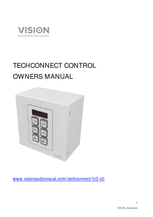
TECHCONNECT CONTROL OWNERS MANUAL/techconnect/tc3-ctlDECLARATION OF CONFORMITYWhere applicable Vision products are certified and comply with all known local regulations to a ‘CB Certification’ standard. Vision commits to ensure all products are fully compliant with all applicable certification standards for sale in the EU and other participating countries.The product described in this owner manual is in compliance with RoHS (EU directive2002/95/EC), and WEEE (EU directive 2002/96/EC) standards. This product should be returned to the place of purchase at the end of its useful life for recycling.WARNINGSCAUTION: TO REDUCE THE RISK OF ELECTRIC SHOCK DO NOT REMOVE COVER (OR BACK). NO USER-SERVICEABLE PARTS INSIDE. REFER SERVICING TO QUALIFIEDSERVICE PERSONNEL.The lightning flash with arrowhead symbol, within an equilateral triangle, is intended to alert theuser to the presence of uninsulated “dangerous voltage” within the product’s enclosure that may beof sufficient magnitude to constitute a risk of electric shock to persons.The exclamation point within an equilateral triangle, is intended to alert the user to the presence ofimportant operating and maintenance (servicing) instructions in the literature accompanying theappliance.WARNING: TO REDUCE THE RISK OF FIRE OR ELECTRIC SHOCK, DO NOT EXPOSETHIS APPLIANCE TO RAIN OR MOISTURE.All products are designed and imported into the EU by ‘Vision’ who is wholly owned by ‘Azlan Logistics Ltd.’, Registered in England Nr. 04625566 at Lion House, 4 Pioneer Business Park, Clifton Moor, York, YO30 4GH. WEEE Registration: GD0046SYDECLARATION OF ORIGINAll Vision products are made in the People’s Republic of China (PRC).USE ONLY DOMESTIC AC OUTLETSConnecting the unit to an outlet supplying a higher voltage may create a fire hazard.HANDLE THE POWER CORD WITH CAREDo not disconnect the plug from the AC outlet by pulling the cord; always pull the plug itself. Pulling the cord may damage it. If you do not intend to use your unit for any considerable length of time, unplug the unit. Do not place furniture or other heavy objects on the cord, and try to avoid dropping heavy objects on it. Do not tie a knot in the power cord. Not only could the cord be damaged, but a short circuit could also be caused with a consequent fire hazard. PLACE OF INSTALLATIONAvoid installing this product under the following conditions:• Moist or humid places• Places exposed to direct sunlight or close to heating equipment• Extremely cold locations• Places subject to excessive vibration or dust• Poorly ventilated placesDo not expose this product to dripping or splashing. DO NOT PLACE OBJECTS FILLED WITH LIQUIDS ON OR NEAR THIS PRODUCT!MOVING THE UNITBefore moving the unit, be sure to pull out the power cord from the AC outlet and disconnect the interconnection cords with other units.WARNING SIGNSIf you detect an abnormal smell or smoke, turn this product off immediately and unplug the power cord. Contact your reseller or Vision.PACKAGINGSave all packing material. It is essential for shipping in the event the unit ever needs repair.IF ORIGINAL PACKAGING IS NOT USED TO RETURN THE UNIT TO THE SERVICE CENTRE, DAMAGE IN TRANSIT WILL NOT BE COVERED BY WARRANTY.FRONT AND REAR PANELS1. Learn Confirmation LED (green)2. Learn Mode LED (red)3. IR Receiver4. Internal IR Blaster / Emitter5. Function Buttons6. RS-2327. PWR in (12V 0.5A)8. 12V Trigger out9. RS-48510. IR outBUTTONS1546789101 23 45 6CONTROL OPTIONS IRTechconnect Control learns and replicates codes sent from a device’s infrared remote control. An IR emitter integrated into the front panel is adequate for small rooms.For larger rooms three external wired IR emitters are included – one with a 10m cable, and two without cables. Techconnect Minijack cables are suitable to extend these.RS-232Professional control format used to control a variety of devices including projectors. Morereliable than IR and uses two-way communication with the control device to confirm commands has been received.Requires 3-core cable.12v TriggerSimple trigger voltage commonly used to activate projection screens. Requires 2-core unshielded cable.RS-485Using the same codes as RS-232, this protocol offers longer cable distances of around 100m, and only requires 2-core cable. Few AV devices can decode RS-485.If using an additional Control module to extend the keypad this terminal is used to connect the slave module to the master.Note: Tx is normally wired to Rx. Extron requires you to wire Tx to Tx.EXTENDED PANELIf you’re using two devices next to each other they are setup as a master/slave. They connect via RS-485 A to A, B to B.INSTALLATION1. FIT LABELS Use flat-head screwdriver to unclip clear button covers, then apply labels asshown:2.SELECT POWER SOURCE The control module is set to be powered by mains power by default. If you choose to power with 2 x AAA batteries (not included) move switch inside the battery compartment to BATT.3. CONNECT CABLES Connect appropriate cables and fit the module into the surround. In very simple installations it may not be necessary to connect any cables.SIMPLE MODE PROGRAMMINGAppropriate for controlling one IR device only, e.g. projector.1. PUT DEVICE INTO LEARN MODE Press and hold button 3 then press and hold button 4,(middle buttons). The learn LED on the front panel will turn red and stay on.2. PRESS BUTTON TO ASSIGN CODE TO Press function button on the front panel which theincoming code will be assigned to. One code can be assigned to each button.3. TEACH CODE Point remote control at the front panel of Control module. Press and hold thebutton on the remote until the green confirmation LED flashes.If red LED flashes it has failed to learn the code. Try again.4. REPEAT The device will revert back to normal mode once it has learnt a code. Repeat stepsabove to program other buttons.ADVANCED MODE PROGRAMMINGUse when you need to•Program multiple codes to each button•Use RS-232 or 12v trigger•Add an extension keypad•Program scheduled actions•Duplicate to multiple devices1.LOAD SOFTWARE ONTO PC Download from Vision’s website:/techconnect/tc3-ctl2.CONNECT CONTROL MODULE VIA USB In the battery compartment there is a standardUSB-B mini connector. (USB cable not included)The software can be used without a control module connected, but if learning IR codes you will need to connect a control module.UNCH SOFTWARE You can create a new program, edit program saved on PC, or editprogram saved on device.To find firmware version of your device click “Read CTL3Time”4.START BY ASSIGNING CODES click a button on the image. This window allows you to set the codes for that button 1.5.SELECT EXISTING CODES If codes are already in the library then select the device and function in the drop-down menus. The code will appear.Repeat: when you hold the button down the codes are repeatedly sent Sequential: 1st press sends command 1, 2nd press sendscommand 2, etc.Simultaneous: All commands are send at the same time Select RS-232 / IR / 12V Note: it is not possible to seta delay for 12v triggers6.SET UP NEW CODES select “Add New” in any of the device columns. A new windowappears:a.Type over existing text in Device / Brand / Model fields.b.RS-232 only: Baud Rate and Parity settings are normally unchanged. Theprojector manual will advise if they need to be changed.c.Type over existing text in Function fields and enter code.d.If adding IR codes a learn button will be to the right of each code.i.Connect a TC2-CTL3 to PC with a USB cable.ii.Press learn then wait until the red LED lights on the moduleiii.Point original remote at front of module and press and hold buttoniv.Once you have finished the button will be blue to show codes aree. The save button will not un-grey until all fields are complete.f. Click Save. You will have just created a list of new codes, so you need to assign a specific new code to the button using the drop-down menus.Must type a model name before Save is available.7.EDIT CODES Click on edit. You can only edit codes that have been created by users. Thepreset library Vision includes cannot be modified.8.EXTENSION PANELS If six buttons isn’t enough you can use two panels side by side:a.Assign commands to buttons 1-6b.Tick the extension keypadc.Assign commands to buttons 7-12d.Program MASTER (1-6) devicei.Untick boxii.Connect MASTER device to PCiii.Select copy to devicee.Program SLAVE (7-12) devicei.Tick boxii.Connect SLAVE device to PCiii.Select copy to devicef.Connect two devices together with RS-485 terminals. All RS-232, IR, and 12vtrigger cables should be terminated to the master unit.9.SCHEDULE LAST If setting up the scheduling function do this last. All of the codes havebeen learnt first.TROUBLESHOOTINGIf your system is not operating properly, please refer to the following information. If the problem persists, disconnect from power and contact your AV reseller immediately.Problem CorrectionNo LED when buttons pressed •If powered by batteries make sure switch underbatteries set to BATT or PWR as appropriate•Replace batteries. Voltage must be higher than2.8V•Check mains power connection (if using).•If using mains power remove batteries•Make sure codes have been learntModule fails to learn the code •Make sure the original remote is 50mm away fromthe IR receiver on the top/front of the module, andat 90 degrees•Make sure the original remote has fresh batteries.•Hold down the button on the original remote forlonger and release only after the green LED lightson the moduleModule learns code but doesn’t control the projector •Re-program the buttons.•If you programmed in simple mode tryprogramming in advanced mode•Use external IR blaster•Check IR blaster cable to make sure it hasn’t been damagedSPECIFICATIONSPRODUCT DIMENSIONS: 71 x 42 x 31mm (length x width x height)PRODUCT WEIGHT: 63 gramsCONSTRUCTION MATERIAL: PlasticCOLOUR: WhitePOWER SUPPLY: 100-240v AC 50/60Hz 12 volt / 0.5 ampTransformer integrated into plug. Includes interchangeable plugs: UK/EU/US/AU. DC tail length: 4m. Transformer dimensions: 66 x 43 x 30mmPOWER CONSUMPTIONStatic: <= 5uASending: <= 20mACopying: <= 10MaCOMPLIANCE: RoHS, WEEE & CE CompliantACCESSORIES INCLUDED5 x Blanking buttons1 x Labels1 x Single-Gang Techconnect Backbox1 x Single-Gang Techconnect Surround1 x IR Blaster with 150mm cable (terminated with female minijack)1 x IR Blaster with 20m cable1 x RS-232 male D-Sub to phoenix 150mm cableWARRANTYThis product comes with a 2-year return to base warranty, effective from the date of purchase. This warranty applies only to the original purchaser and is not transferable. For the avoidance of doubt, this will be taken from the information held by the appointed national distributor at the point of sale. If the product is DOA (dead on arrival), you have 21 days from purchase date to notify the national distributor via your AV reseller. The liability of the manufacturer and its appointed service company is limited to the cost of repair and/or replacement of the faulty unit under warranty, except for death or injury (EU85/374/EEC). This warranty protects you against the following:• Failure of any components, including the power supply.• Damage when the product is first removed from its packaging if reported within 24 hours of purchase.If you find you do have a problem with this product, you should contact the AV reseller you purchased this product from. The original purchaser is responsible for shipment of the product to the manufacturer’s appointed service centre for repair.We will endeavour to return repaired units within 5 working days, however this may not always be possible, in which case it will be returned as soon as practicably possible. In line with our WEEE commitments, the manufacturer endeavours to replace the faulty parts of the product rather than replacing the whole unit. This warranty does not protect this product against faults caused by abuse, misuse, incorrect installation, unstable or faulty power input, which might be caused by ignoring the guidelines set out in this manual.LEGAL DISCLAIMER: Because we are committed to improving our products, the details above may change without prior warning. This User Manual is published without warranty and any improvements or changes to the User Manual necessitated by typographical errors, inaccuracies of current information, or improvements to programs and/or equipment, may be made at any time and without notice. Such changes will be incorporated into new editions of the User Manual.。
- 1、下载文档前请自行甄别文档内容的完整性,平台不提供额外的编辑、内容补充、找答案等附加服务。
- 2、"仅部分预览"的文档,不可在线预览部分如存在完整性等问题,可反馈申请退款(可完整预览的文档不适用该条件!)。
- 3、如文档侵犯您的权益,请联系客服反馈,我们会尽快为您处理(人工客服工作时间:9:00-18:30)。
Chapter 8 Contact and InterconnectionI.Contact and Interconnection–Increasing importance forVLSI/ULSI TechnologyII. Advanced Contact & Interconnection Technology –Integration of various thin film materials and process techniquesIII. Contact ResistanceIV. Al/Si Ohmic Contact and InterconnectV. Cu Interconnection by Damascene TechnologyVI. Silicide. Polycide and SalicideChapter 8 Contact and InterconnectionI. Contact and Interconnection–Increasing importance forVLSI/ULSI TechnologyRequirements and problems of C&I for IC Progress(1) High Speed:Low interconnect resistanceLow contact resistanceLow capacitanceProblem: RC ↑wt L R ρ= (+ Contact resistance)ii t Lw C ε= (+ Line-to-Line C) i i s t R L RC ε2= ↑(2) High reliabilityUniform metal/Si interfaceLow electromigrationProblem:-- Metal/Si: interdiffusion &interaction ÆAl “Spiking” –Contactfailure-- Electromigration – void formation– interconnect failure(3) High density-- Smaller contact, more narrow metal line-- Multilevel metallizationNPG A 3/2=A – Chip areaG – Number of IC gatesP – Metal pitch (line width + space )N – Number of metal levelsProblems: Increasing process complexity∴C&I – One of the bottlenecks for deep sub µ IC technology!II. Advanced Contact & Interconnection Technology –Integration of various thin film materials and process techniques1.Various materials for C&Iz For early IC: Alz At medium stage: (≥2-3 µm)Al + Doped Poly-Siz For Advanced VLSI/ULSI:(1)High conductive metal & itsalloy: Al, Al-Si, Al-Si-Cu, Cu(2) Heavily doped poly Si: n+-Poly-Si, p+-Poly-Si(3) Refractory metals: W, Ta ...(4) Metal silicide: TiSi2 , CoSi2 ,PtSi , NiSi, WSi2(5) Other metal alloy and compound: TiN , WN …+ Different dielectric films:Inorganic: SiO2 , PSG , BSG , BPSGOrganic polymersbination of various processing technology(1) Self-aligned technology:*Self-aligned poly-Si gate and polycide gate technology*Self-aligned silicide contact and gate technology (salicide)(2) Diffusion barrier technology(3) Multilevel interconnectionCMOS: 0.5 µm---3-4 Levels; 0.35 µm---4-5 Levels;130nm--8Levels; 90nm--9Levels; 65nm--10Levels (by ITRS2001) (4) Layered matallization structureSi (Al) / Contact (adhesion) layer/ Diffusion barrier layer/ Vertical interconnect/ Lateral interconnect/ Anti-reflection (capping) coating(5) New materials and process techniques supporting above technologiesz Typical cross section of future advanced CMOS interconnectionFuture C & ITechnologydepends on:*Introduction ofnew materials*Integration ofnew processes andstructures3.Various thin film deposition, formation and etchingtechnologiesSputteringEvaporationCVDSolid state reactionReactive ion etchingSelective etching (wet & dry)Planarization techniques: CMP; Etching back process 4.Requirements for Gate Electrode and InterconnectsMaterials-- Low resistivity-- High temperature stability (~1000°C)-- Fine line etching capability-- Easy to passivation-- Chemical stability to the commonly used solutions in IC process-- Low contact resistance with Si & metals-- Resistance to Electromigration5. Requirements for Ohmic Contacts-- Low contact resistivity-- Limited interface interaction-- Interface uniformity-- Stabilityz RC Delay Time of 1 cm interconnect line on SiO 2 (1 µm) / Si for different materialsMaterial Resistivity (µΩ·cm)Thickness (nm)R S (Ω/□)RC (ns/cm)Al 2.72500.110.4Cu 2.02500.080.3W 82500.32 1.1Mo 82500.32 1.1TiSi 2152500.6 2.1CoSi 2152500.6 2.1NiSi 152500.62.1WSi 270250 2.89.7MoSi 2~100250413.8TaSi 255250 2.27.6TiN 502502 6.9PolySi ~10005002069III. Contact ResistanceTwo types of M/Si contactsSchottky contact on n --SiOhmic contact on n +-Siz ForN D ≤1017cm -3 Current flow bythermionic emission]1))[exp(/exp(2*−−=KTqV KT q T A J B φA*: Richardson constant; ΦB : Barrier heightz Specific contact resistance (R c ))exp(*0KTq T qA K dJ dV R BV c φ=== [Ω·cm 2] If ΦB =0.85V → R c =4.7x10⁵Ω·cm 2ΦB =0.25V → R c =4x10⁻⁷Ω·cm 2R c (on p-Si) < R c (on n-Si)z For N D > 1019cm -3: Current flow by carrier tunneling)](*4exp[DB c N h m A R φεπ≈ ε – Dielectric permittivity;m* – Effective mass of carrierA – ConstantExample:If 26101cm R c•Ω×≈−; for contact hole µµ11×→ Ω==−−100)10(10246R Ω=×400:5.05.0R µµ∴Lower R c is needed for deepsub-µ CMOSz Total resistance of a contactr=r s +r c r s – spreading resistance ofsemiconductor under contact (Ω)r c – contact resistance (Ω)Both r s , r c depend on doping and contact size▲ Typical value of total resistance for a contact: r ≈ 10-100Ω/contact▲ With shrinkage of contact size lower specific contact resistance is requiredIV. Al/Si Ohmic Contact and Interconnect1. Al -- Extensively used interconnect material for IC-- No.3 material for Si devices fabrication after Si, SiO2▲ Low Resistivity: P ≈2.7Ω·cm▲ Compatibility with Si & SiO2Good adhesion with SiO2 due toslight reaction to form Al2O3 atAl/SiO2 interface▲ Mature Al processing technologyDeposition (evaporation Æsputtering)Etching (wet Æ dry)2.Two problems(1) Al spikingAl melting point -- 660°CAl-Si eutectic T-- 577°CAt T< 577°C:z High solubility & diffusivity of Si inAl: Æ “Etching” of Si by AlÆ Si, Al interdiffustionÆ Pits in Si surface Æ Al-SpikingÆ pn junction failurez Orientation effect of Al spiking▲ A Spiking is more severe on (100)Si-substrate▲ Reason –anisotropical Al/Siinterface interaction▲ “Etching” of Si by metal (likewet etching) – slow etchingplanes – {111} Æ (111) planes actas an etch stop (slow dissolvingplanes)*(111)Si: Triangular pits*(100)Si: Square – toppedpyramidal pitsIn practice : due to residual interfacial SiOx Æ nouniform interaction Æ Spiking▲ Alloy transistors of Si & Ge were made on (111) substrate(2)Al Electromigration▲ Effect of momentum transfer from electron to metal ions Noticeable in the case of high current density (In IC, current density may: j ≈105 A/cm 2)▲ Metal ion transport flux, j mKT j e NDZ j m ρ*=N – Density of metal ionsD – Self-diffusion coeff. of metalZ* -- Effective charge of ionΡ – Resistivity of metalJ – current density in meta lÆ Hillocks growth toward the positive endVoids formation near the negative end of the lead Æ Interconnect break, IC failure▲ Temperature dependence of electromigration failure KT E a eD D /0−=E a – Diffusion activation energyMTF – median time to failureKT E m a e j A MTF /'−= A’ – constant, m ≈1-3 Experimental MTF for Al evaporated on cold sub. KTeABj MTF /48.0216)(101.4−×= A – Cross section of Al line (cm 2)B – 1 A 2·hr/cm 6 (a unit conversation constant) For Al evap. on hot sub Ægrain ÇÆE a Ç(~0.7eV)ÆMTF Ç▲ Stress induced migration failure3. Improvement of Al metallization(1) Al-Si alloy: Al + 0.5-2% Si*Reduce Si-dissolution into Al*Problems: -- Resistivity increasing ;– Al-doping Æp-type ÆR c Ç(2) Al-Cu Alloy (+0.5-4% Cu)Reduce Al electromigration Æ MTF ÇProblems : ρÇ, Dry etching difficulty(3) Diffusion barrier between Si & Al: TiW, TiN, TaN…V. CuInterconnection byDamasceneTechnologyz Typical Cu-interconnectionprocessing:(a)沟槽刻蚀(b) TiN, Cu 淀积(c) 化学机械抛光(d) 过抛蚀(e) TiWN淀积(f) 化学机械抛光z Dual Cu Damascene ProcessFormation of vertical(via) andlateral interconnection(line) bycombined Cu damascene processz Combination of Cuinterconnection with low Kdielectrics material andprocess—key of the success of future advancedinterconnection technologyVI. Silicide. Polycide and Salicide1.Metal Silicides -- Important Si based materials for ULSI (1)Type of silicides:Variety of differentsilicides (>200)z Transition metalsilicides*Refractory metalsilicides (from IVb, Vb,VIb refractory metals)-- TiSi2,WSi2,MoSi2,TaSi2 …-- Formation T ≥600°C-- High melting point-- Diffusion species during formation – Si*Near-Noble metal silicides (from VIII group metals)-- CoSi2,NiSi2,PtSi,NiSi,Pd2Si …-- Formation T lower (200 - 600°C)-- Lower melting point-- Diffusion species during formation –Si, or metal(2) Properties interesting for IC application-- Metal-like high conductivity (10-100 µΩ)-- High T thermal stability-- Good chemical stability (in oxidizing ambient, wet & plasma chemicals)-- Uniform silicide / Si interface▲ Low leakage Schottky barrier contact▲ Low contact resistance Ohmic contact(3) Variety of application for microelectronics-- SBD devices for bipolar IC-- Ohmic contact-- Gate electrode for self-aligned device technology in both Si-MOS and GaAs-MESFET-IC-- Low barrier devices for infrared detector (PtSi/p-Si…) -- Local interconnect2. Silicide Film Formation Method(1) Solid state reaction of M/S-- Different phase at different T-- MSix/Si interface formed beneath original Si surface-- Lower ρ than deposited film-- Possible impurity segregation during reaction-- Consumption of Si: mM+nSi Æ M m Si n(t m) (t si) (t silicide)TiSi2 1.00 2.24 2.50CoSi2 1.00 3.63 3.49PtSi 1.00 1.32 1.98NiSi 1.00 1.84 2.22Pd2Si 1.00 0.68 1.42 (2) Physical depositon-- Sputtering from composite targets-- Co-sputtering (or co-evaporation) from elemental targets -- Low ρ phase formation by thermal annealing-- composition and stoichiometry control(3) CVD-- By chemical reaction Æ WSi2, TiSi2, TaSi2, MoSi2*WF6(vapor) + 2SiH4(vapor) Æ WSi2(solid) +6HF + H2*TiCl6+ 2SiH4Æ TiSi2 +4HCl+2H2-- Better step coverage, higher purity and higher throughput -- CVD WSi2 – more applicationAs-deposited film ρ≈600-900 µΩ·cmAfter annealing ρ≈35-80 µΩ·cm-- Commercial cold-wall system available3. Polycide – Composite structure of silicide on poly-Si▲ Polycide process technology-- Poly-Si deposition & doping-- Silicide (e.g. WSi2) depositionby CVD or PVD-- Thermal annealing-- Gate mask lithography-- Reactive ion etching (RIE) of WSi 2 and poly-Si-- S/D implant▲ Advantages-- Low gate resistance20-30 Ω⁄□ Æ 1-4Ω⁄□ (Depends on thickness)-- Remain excellent PolySi/SiO 2/Si interface-- Poly-Si pad prevents metal diffusion into gate oxide -- Possibility of growing stable SiO 2 ° SiO 2 formation with unchanged silicide film (WSi 2,TiSi 2 …) by Si consumption from poly-Si layer° Oxide growth may follow similar kinetics)(2τ+=+t B AX X or BtX =2 For WSi 2/PolySi: BtX =82.1▲ Applications-- High density memory chips, DRAM, SRAM; -- ASICs 4. Salicide – Self-aligned Silicide Technology(1) Main process steps:-- Self-aligned PolySi & S/Dprocess-- Dielectric deposition-- RIE Æ sidewall dielectricformation on poly-Si line-- Metal deposition by sputtering (Ti, Co …)-- 1st step annealing by RTA at lower T Æ reaction oncrystalline Si(S/D) and poly-Si(G)-- Selective etching Æ Remove metal from FOX and sidewall -- 2nd step annealing by RTA at higher T Æ Formation highconductive silicide phase(2) Key technology-- Solid state reaction of metal with both C-Si & Poly-Si ° Ti/Si, Co/Si, Pt/Si, Ni/Si° Elimination of lateral growth-- No reaction with SiO 2-- Integrity of Poly-Si and S/D junctions(3) Advantages-- A self-aligned technology –simultaneous silicidation of S/D region & gate line-- Significant reduction of R□ & Rc of S/D regions-- Significant reduction of gate level interconnects-- Remain excellent PolySi/SiO2/Si interface-- Good for small geometry & shallow junction devices Improve density, speed and reliability-- Possibility for developing new technology for VLSI(4) Silicides for Salicide Technologyz Ti/Si Æ TiSi2▲Most common used▲ Low resistivity (C54 phase)▲ Easy to formProblem: Difficulty in transformation of C49 Æ C54 for small geometry lines(<0.25µm)z Co/Si Æ CoSi2▲ Already application by some companies▲ As Low resistivity as TiSi2▲ More chemically stable▲ Close lattice structure withSi Æ possible epi. GrowthProblem: Consume more Si thanTiSi2, for the same R□, ~16% more Siz Ni/Si Æ NiSi▲L ow resistivity▲L ow Si consumptionProblem: Low thermal stability;non-maturePossible application for CMOSbelow 90nm with lower back–end processing TIntensive R&D of salicide material & technology for nanometer scale CMOS fabrication(From Dr. K. Han’s report at WIMNCT-2002)。