RB751S40;中文规格书,Datasheet资料
B0540WS-7;中文规格书,Datasheet资料
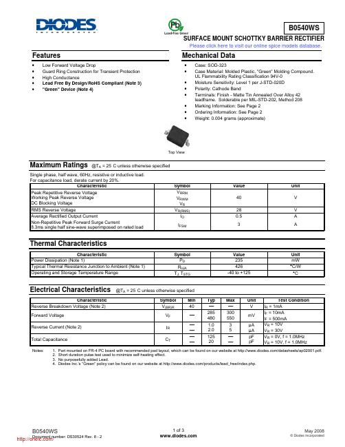
SURFACE MOUNT SCHOTTKY BARRIER RECTIFIERFeatures• Low Forward Voltage Drop• Guard Ring Construction for Transient Protection • High Conductance• Lead Free By Design/RoHS Compliant (Note 3) • "Green" Device (Note 4)Mechanical Data• Case: SOD-323• Case Material: Molded Plastic, "Green" Molding Compound.UL Flammability Rating Classification 94V-0• Moisture Sensitivity: Level 1 per J-STD-020D• Polarity: Cathode Band• Terminals: Finish - Matte Tin Annealed Over Alloy 42leadframe. Solderable per MIL-STD-202, Method 208 • Marking Information: See Page 2• Ordering Information: See Page 2• Weight: 0.004 grams (approximate)Top ViewMaximum Ratings@T A = 25°C unless otherwise specifiedSingle phase, half wave, 60Hz, resistive or inductive load.For capacitance load, derate current by 20%.Characteristic Symbol Value UnitPeak Repetitive Reverse Voltage Working Peak Reverse Voltage DC Blocking Voltage V RRMV RWMV R40 VRMS Reverse Voltage V R(RMS)28 V Average Rectified Output Current I O0.5 ANon-Repetitive Peak Forward Surge Current8.3ms single half sine-wave superimposed on rated load I FSM3 A Thermal CharacteristicsCharacteristic Symbol Value Unit Power Dissipation (Note 1) P D235 mW Typical Thermal Resistance Junction to Ambient (Note 1) RθJA426 °C/W Operating and Storage Temperature Range T J, T STG-40 to +125 °CElectrical Characteristics@T A = 25°C unless otherwise specifiedCharacteristic Symbol Min Typ Max Unit Test Condition Reverse Breakdown Voltage (Note 2) V(BR)R40 ⎯⎯V I R = 1mAForward Voltage V F⎯285480300550mVI F = 10mAI F = 500mAReverse Current (Note 2) I R ⎯⎯1.02.035μAμAV R = 10VV R = 30VTotal Capacitance C T ⎯⎯12520⎯⎯pFpFV R = 0V, f = 1.0MHzV R = 10V, f = 1.0MHzNotes: 1. Part mounted on FR-4 PC board with recommended pad layout, which can be found on our website at /datasheets/ap02001.pdf.2. Short duration pulse test used to minimize self-heating effect.3. No purposefully added Lead.4. Diodes Inc.'s "Green" policy can be found on our website at /products/lead_free/index.php.Please click here to visit our online spice models database.10100V, INSTANTANEOUS REVERSE VOLTAGE (V)Fig. 2 Typical Reverse CharacteristicsRI,INSTANTANEOUSFORWARDCURRENT(mA)FV, INSTANTANEOUS FORWARD VOLTAGE (V)Fig. 1 Typical Forward CharacteristicsF100C,TOTALCAPACITANCE(pF)TV, DC REVERSE VOLTAGE (V)Fig. 3 Total Capacitance vs. Reverse VoltageR0.250.50050100I,AVE150RAGEFORWARDCURRENT(A)F(AV)T, TERMINAL TEMPERATURE (C)Fig. 4 Forward Current Derating CurveT°0.751.02575125Ordering Information(Note 5)Part Number Case PackagingB0540WS-7 SOD-323 3000/Tape & ReelNotes: 5. For packaging details, go to our website at /datasheets/ap02007.pdf.Marking InformationSF SF = Product Type Marking CodePackage Outline DimensionsSuggested Pad LayoutIMPORTANT NOTICEDiodes Incorporated and its subsidiaries reserve the right to make modifications, enhancements, improvements, corrections or other changes without further notice to any product herein. Diodes Incorporated does not assume any liability arising out of the application or use of any product described herein; neither does it convey any license under its patent rights, nor the rights of others. The user of products in such applications shall assume all risks of such use and will agree to hold Diodes Incorporated and all the companies whose products are represented on our website, harmless against all damages.LIFE SUPPORTDiodes Incorporated products are not authorized for use as critical components in life support devices or systems without the expressed written approval of the President of Diodes Incorporated.SOD-323 Dim Min Max A 0.25 0.35 B 1.20 1.40 C 2.30 2.70 H 1.60 1.80 J 0.00 0.10 K 1.0 1.1 L0.20 0.40 M 0.10 0.15α0° 8°All Dimensions in mmDimensions Value (in mm)Z 3.75 G 1.05 X 0.65 Y 1.35 C 2.40分销商库存信息: DIODESB0540WS-7。
NCV7517BFTR2G;中文规格书,Datasheet资料
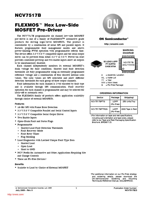
NCV7517BFLEXMOS t Hex Low-Side MOSFET Pre-DriverThe NCV7517B programmable six channel low−side MOSFET pre−driver is one of a family of FLEXMOS TM automotive grade products for driving logic−level MOSFETs. The product is controllable by a combination of serial SPI and parallel inputs. It features programmable fault management modes and allows power−limiting PWM operation with programmable refresh time. The device offers 3.3 V/5.0 V compatible inputs and the serial output driver can be powered from either 3.3 V or 5.0 V. Power−on resetprovides controlled powerup and two enable inputs allow all outputs to be simultaneously disabled.Each channel independently monitors its external MOSFET’s drain voltage for fault conditions. Shorted load fault detection thresholds are fully programmable using an externally programmed reference voltage and a combination of four discrete internal ratio values. The ratio values are SPI selectable and allow different detection thresholds for each group of three output channels.Fault information for each channel is 2−bit encoded by fault type and is available through SPI communication. Fault recovery operation for each channel is programmable and may be selected for latch−off or automatic retry.The FLEXMOS family of products offers application scalability through choice of external MOSFETs.Features•16−Bit SPI with Frame Error Detection•3.3 V/5.0 V Compatible Parallel and Serial Control Inputs •3.3 V/5.0 V Compatible Serial Output Driver•Two Enable Inputs•Open−Drain Fault and Status Flags•Programmable−Shorted Load Fault Detection Thresholds−Fault Recovery Mode−Fault Retry Timer−Flag Masking•Load Diagnostics with Latched Unique Fault Type Data−Shorted Load−Open Load−Short to GND•NCV Prefix for Automotive and Other Applications Requiring Site and Change Controls•These are Pb−Free Devices*Benefits•Scalable to Load by Choice of External MOSFET32 LEAD LQFPFT SUFFIXCASE 873AMARKINGDIAGRAMDevice Package Shipping†ORDERING INFORMATIONNCV7517BFTG LQFP(Pb−Free)250 Units/Tray†For information on tape and reel specifications, including part orientation and tape sizes, please refer to our T ape and Reel Packaging Specification Brochure, BRD8011/D.NCV7517BAWLYYWWGA= Assembly LocationWL= Wafer LotYY= YearWW= Work WeekG= Pb−Free PackageNCV7517BFTR2G LQFP(Pb−Free)2000 T ape & Reel*For additional information on our Pb−Free strategy and soldering details, please download the ON Semiconductor Soldering and Mounting T echniques Reference Manual, SOLDERRM/D.Figure 1. Block DiagramFigure 2. Application DiagramPIN FUNCTION DESCRIPTIONSymbol DescriptionFLTREF Analog Fault Detect Threshold: 5.0 V Compliant DRN0 – DRN5Analog Drain Feedback: Internally ClampedGAT0 – GAT5Analog Gate Drive: 5.0 V CompliantENA1, ENA2Digital Master Enable Inputs: 3.3 V/5.0 V (TTL) CompatibleIN0 – IN5Digital Parallel Input: 3.3 V/5.0 V (TTL) CompatibleCSB Digital Chip Select Input: 3.3 V/5.0 V (TTL) CompatibleSCLK Digital Shift Clock Input: 3.3 V/5.0 V (TTL) CompatibleSI Digital Serial Data Input: 3.3 V/5.0 V (TTL) CompatibleSO Digital Serial Data Output: 3.3 V/5.0 V CompliantSTAB Digital Open−Drain Output: 3.3 V/5.0 V CompliantFLTB Digital Open−Drain Output: 3.3 V/5.0 V CompliantVCC1Power Supply − Low Power PathGND Power Return − Low Power Path – Device SubstrateVCC2Power Supply − Gate DriversVDD Power Supply − Serial Output DriverVSS Power Return – VCC2, VDD, Drain ClampsFigure 3. 32 Pin LQFP Pinout (Top View)MAXIMUM RATINGS(Voltages are with respect to device substrate.)Rating Value UnitDC Supply (V CC1, V CC2, V DD)−0.3 to 6.5V Difference Between V CC1 and V CC2"0.3V Difference Between GND (Substrate) and V SS"0.3VOutput Voltage (Any Output)−0.3 to 6.5VDrain Feedback Clamp Voltage (Note 1)−0.3 to 47VDrain Feedback Clamp Current (Note 1)10mAInput Voltage (Any Input)−0.3 to 6.5V Junction T emperature, T J−40 to 150°C Storage T emperature, T STG−65 to 150°CPeak Reflow Soldering T emperature: Lead−Free60 to 150 seconds at 217°C (Note 2)260 peak°CStresses exceeding Maximum Ratings may damage the device. Maximum Ratings are stress ratings only. Functional operation above the Recommended Operating Conditions is not implied. Extended exposure to stresses above the Recommended Operating Conditions may affect device reliability.ATTRIBUTESCharacteristic ValueESD CapabilityHuman Body Model Machine Model w" 2.0 kV w" 200 VMoisture Sensitivity (Note 2)MSL3 Package Thermal Resistance (Note 3)Junction–to–Ambient, R q JA Junction–to–Pin, R Y JL 86.0 °C/W 58.5 °C/W1.An external series resistor must be connected between the MOSFET drain and the feedback input in the application. Total clamp powerdissipation is limited by the maximum junction temperature, the application environment temperature, and the package thermal resistances.2.For additional information, see or download ON Semiconductor’s Soldering and Mounting T echniques Reference Manual, SOLDERRM/D, andApplication Note AND8003/D.3.Values represent still air steady−state thermal performance on a 4 layer (42 x 42 x 1.5 mm) PCB with 1 oz. copper on an FR4 substrate, usinga minimum width signal trace pattern (384 mm2 trace area).RECOMMENDED OPERATING CONDITIONSSymbol Parameter Min Max Unit V CC1Main Power Supply Voltage 4.75 5.25V V CC2Gate Drivers Power Supply Voltage V CC1− 0.3V CC1+ 0.3VV DD Serial Output Driver Power Supply Voltage 3.0V CC1V V IN High Logic High Input Voltage 2.0V CC1V V IN Low Logic Low Input Voltage00.8VT A Ambient Still−Air Operating T emperature−40125°CELECTRICAL CHARACTERISTICS (4.75 V v V CCX v5.25 V, V DD = V CCX, −40°C v T J v125°C, unless otherwise specified.) (Note 4) Characteristic Symbol Conditions Min Typ Max Unit V CC1 SupplyOperating Current –V CC1= 5.25 V, V FLTREF=1.0 V ENA X= 0ENA1= ENA2= V CC1,V DRNX= 0 V, GAT X drivers offENA1= ENA2= V CC1,GAT X drivers on–––2.803.102.805.05.05.0mAPower−On Reset Threshold V CC1 Rising 3.65 4.20 4.60V Power−On Reset Hysteresis−0.1500.385–V Digital I/OV IN High ENA X, IN X, SI, SCLK, CSB 2.0––V V IN Low ENA X, IN X, SI, SCLK, CSB––0.8V V IN Hysteresis ENA X, IN X, SI, SCLK, CSB100330500mV Input Pullup Current CSB V IN= 0 V−25−10–m A Input Pulldown Current ENA2, IN X, SI, SCLK,V IN= V CC1–1025m A Input Pulldown Resistance ENA1100150200k W SO Low Voltage V DD= 3.3 V, I SINK= 5.0 mA–0.110.25VSO High Voltage V DD= 3.3 V, I SOURCE= 5.0 mA V DD−0.25V DD−0.11–VSO Output Resistance Output High or Low–22–W SO Tri−State Leakage Current CSB = 3.3 V−10–10m A STAB Low Voltage STAB Active, I STAB= 1.25 mA–0.10.25V STAB Leakage Current V STAB= V CC1––10m A FLTB Low Voltage FLTB Active, I FLTB= 1.25 mA–0.10.25V FLTB Leakage Current V FLTB= V CC1––10m A Fault Detection – GAT X ONFLTREF Input Current V FLTREF=0 V−1.0––m A FLTREF Input Linear Range(Note 5)0–V CC1−2.0V FLTREF Op−amp V CC1 PSRR(Note 5)30––dBDRN X Clamp Voltage V CL I DRNX= 10 m AI DRNX= I CL(MAX) = 10 mA 27–3442–47VDRN X Shorted Load Threshold GAT X Output HighV FLTREF= 1.0 V Register 2: R1= 0, R0= 0 orR4= 0, R3= 0202530%V FLTREF Register 2: R1= 0, R0= 1 orR4= 0, R3= 1455055%V FLTREF Register 2: R1= 1, R0= 0 orR4= 1, R3= 0707580%V FLTREF Register 2: R1= 1, R0= 1 orR4= 1, R3= 195100105%V FLTREFDRN X Input Leakage Current V CC1= V CC2= V DD= 5.0 V,ENA X= IN X= 0 V,V DRNX = V CL(MIN)V CC1= V CC2= V DD= 0 V,ENA X= IN X= 0 V,V DRNX = V CL(MIN)−1.0– 1.0m A4.Designed to meet these characteristics over the stated voltage and temperature recommended operating ranges, though may not be 100%parametrically tested in production.5.Guaranteed by design.Characteristic Symbol Conditions Min Typ Max UnitFault Detection – GAT X OFFDRN X Diagnostic Current I SG Short to GND Detection,V DRNX= 0.30 V CC1−27−20−10m AI OL Open Load Detection,V DRNX= 0.75 V CC1306080m A DRN X Fault Threshold Voltage V SG Short to GND Detection273033%V CC1V OL Open Load Detection727578%V CC1DRN X Off State Bias Voltage V CTR−–50–%V CC1 Gate Driver OutputsGAT X Output Resistance Output High or Low200350500W GAT X High Output Current V GATX = 0 V−26.25–−9.5mA GAT X Low Output Current V GATX = V CC29.5–26.25mATurn−On Propagation Delay t P(ON)IN X to GAT X (Figure 4)–– 1.0m sCSB to GAT X (Figure 5)Turn−Off Propagation Delay t P(OFF)IN X to GAT X (Figure 4)–– 1.0m sCSB to GAT X (Figure 5)Output Rise Time t R20% to 80% of V CC2,C LOAD = 400 pF(Figure 4, Note 5)––277nsOutput Fall Time t F80% to 20% of V CC2,C LOAD = 400 pF(Figure 4, Note 5)––277nsFault TimersChannel Fault Blanking Timer t BL(ON)V DRNX = 5.0 V; IN X rising toFLTB falling (Figure 6)112131m st BL(OFF)V DRNX = 0 V; IN X falling toFLTB falling (Figure 6)90120150m s Channel Fault Filter Timer t FF Figure 77.01217m sGlobal Fault Refresh Timer (Auto−retry Mode)t FR Register 2: Bit R2= 0 or R5= 07.51012.5ms Register 2: Bit R2 = 1 or R5 = 1304050msTimer Clock ENA1 = 1–500–kHzSerial Peripheral Interface (Figure 9) V ccx = 5.0 V, V DD = 3.3 V, F SCLK = 4.0 MHz, C LOAD = 200 pFSO Supply Voltage V DD 3.3 V Interface 3.0 3.3 3.6V5.0 V Interface 4.5 5.0 5.5VSCLK Clock Period−–250–nsMaximum Input Capacitance Sl, SCLK (Note 7)––12pFSCLK High Time SCLK = 2.0 V to 2.0 V125––nsSCLK Low Time SCLK = 0.8 V to 0.8 V125––nsSl Setup Time Sl = 0.8 V/2.0 V toSCLK = 2.0 V (Note 7)25––nsSl Hold Time SCLK = 2.0 V toSl = 0.8 V/2.0 V (Note 7)25––ns6.Designed to meet these characteristics over the stated voltage and temperature recommended operating ranges, though may not be 100%parametrically tested in production.7.Guaranteed by design.Characteristic Symbol Conditions Min Typ Max UnitSerial Peripheral Interface (continued) (Figure 9) V ccx = 5.0 V, V DD = 3.3 V, F SCLK = 4.0 MHz, C LOAD = 200 pF–2550ns SO Rise Time(20% V SO to 80% V DD)C LOAD = 200 pF (Note 9)––50ns SO Fall Time(80% V SO to 20% V DD)C LOAD = 200 pF (Note 9)CSB Setup Time CSB = 0.8 V to SCLK = 2.0 V60––ns(Note 9)75––ns CSB Hold Time SCLK = 0.8 V to CSB = 2.0 V(Note 9)CSB to SO Time CSB = 0.8 V to SO Data Valid–65125ns(Note 9)–65125ns SO Delay Time SCLK = 0.8 V to SO Data Valid(Note 9)Transfer Delay Time CSB Rising Edge to Next1.0––m sFalling Edge (Note 9)8.Designed to meet these characteristics over the stated voltage and temperature recommended operating ranges, though may not be 100%parametrically tested in production.9.Guaranteed by design.Figure 4. Gate Driver Timing Diagram – Parallel InputFigure 5. Gate Driver Timing Diagram – Serial InputFigure 6. Blanking Timing DiagramFigure 7. Filter Timing DiagramFigure 9. SPI Timing Diagram分销商库存信息: ONSEMINCV7517BFTR2G。
RB751SL;中文规格书,Datasheet资料
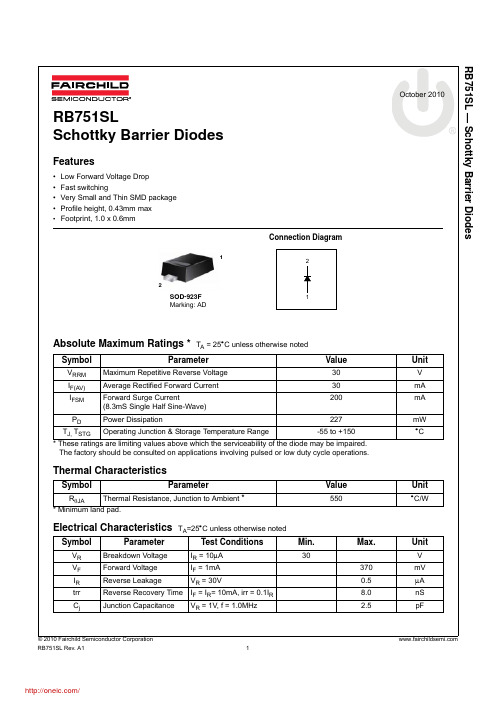
Absolute Maximum Ratings * T A = 25°C unless otherwise noted* These ratings are limiting values above which the serviceability of the diode may be impaired. The factory should be consulted on applications involving pulsed or low duty cycle operations.Thermal Characteristics* Minimum land pad.Electrical Characteristics T A =25°C unless otherwise notedSymbolParameterValueUnitV RRM Maximum Repetitive Reverse Voltage 30V I F(AV)Average Rectified Forward Current 30mA I FSM Forward Surge Current(8.3mS Single Half Sine-Wave)200mA P D Power Dissipation227mW T J, T STGOperating Junction & Storage Temperature Range-55 to +150°CSymbolParameterValueUnitR θJA Thermal Resistance, Junction to Ambient *550°C/WSymbolParameterTest ConditionsMin.Max.UnitV R Breakdown Voltage I R = 10μA 30V V F Forward Voltage I F = 1mA 370mV I R Reverse Leakage V R = 30V0.5μA trr Reverse Recovery Time I F = I R = 10mA, irr = 0.1I R8.0nS C jJunction CapacitanceV R = 1V, f = 1.0MHz2.5pFConnection Diagram2121SOD-923F Marking: ADThe following includes registered and unregistered trademarks and service marks, owned by Fairchild Semiconductor and/or its global subsidiaries, and is notAccuPower¥Auto-SPM¥Build it Now¥CorePLUS¥CorePOWER¥CROSSVOLT¥CTL¥Current Transfer Logic¥DEUXPEED®Dual Cool™ EcoSPARK®EfficientMax¥ESBC¥®Fairchild®Fairchild Semiconductor®FACT Quiet Series¥FACT®FAST®FastvCore¥FETBench¥FlashWriter®*FPS¥F-PFS¥FRFET®Global Power Resource SMGreen FPS¥Green FPS¥ e-Series¥G max¥GTO¥IntelliMAX¥ISOPLANAR¥MegaBuck¥MICROCOUPLER¥MicroFET¥MicroPak¥MicroPak2¥MillerDrive¥MotionMax¥Motion-SPM¥OptoHiT™OPTOLOGIC®OPTOPLANAR®®PDP SPM™Power-SPM¥PowerTrench®PowerXS™Programmable Active Droop¥QFET®QS¥Quiet Series¥RapidConfigure¥¥Saving our world, 1mW/W/kW at a time™SignalWise¥SmartMax¥SMART START¥SPM®STEALTH¥SuperFET®SuperSOT¥-3SuperSOT¥-6SuperSOT¥-8SupreMOS®SyncFET¥Sync-Lock™®*The Power Franchise®TinyBoost¥TinyBuck¥TinyCalc¥TinyLogic®TINYOPTO¥TinyPower¥TinyPWM¥TinyWire¥TriFault Detect¥TRUECURRENT¥*P SerDes¥UHC®Ultra FRFET¥UniFET¥VCX¥VisualMax¥XS™* Trademarks of System General Corporation, used under license by Fairchild Semiconductor.DISCLAIMERFAIRCHILD SEMICONDUCTOR RESERVES THE RIGHT TO MAKE CHANGES WITHOUT FURTHER NOTICE TO ANY PRODUCTS HEREIN TO IMPROVE RELIABILITY, FUNCTION, OR DESIGN. FAIRCHILD DOES NOT ASSUME ANY LIABILITY ARISING OUT OF THE APPLICATION OR USE OF ANY PRODUCT OR CIRCUIT DESCRIBED HEREIN; NEITHER DOES IT CONVEY ANY LICENSE UNDER ITS PATENT RIGHTS, NOR THE RIGHTS OF OTHERS. THESE SPECIFICATIONS DO NOT EXPAND THE TERMS OF FAIRCHILD’S WORLDWIDE TERMS AND CONDITIONS, SPECIFICALLY THE WARRANTY THEREIN, WHICH COVERS THESE PRODUCTS.LIFE SUPPORT POLICYFAIRCHILD’S PRODUCTS ARE NOT AUTHORIZED FOR USE AS CRITICAL COMPONENTS IN LIFE SUPPORT DEVICES OR SYSTEMS WITHOUT THE EXPRESS WRITTEN APPROVAL OF FAIRCHILD SEMICONDUCTOR CORPORATION.As used herein:1. Life support devices or systems are devices or systems which, (a) areintended for surgical implant into the body or (b) support or sustain life, and (c) whose failure to perform when properly used in accordance with instructions for use provided in the labeling, can be reasonably expected to result in a significant injury of the user. 2. A critical component in any component of a life support, device, orsystem whose failure to perform can be reasonably expected to cause the failure of the life support device or system, or to affect its safety or effectiveness.ANTI-COUNTERFEITING POLICYFairchild Semiconductor Corporation's Anti-Counterfeiting Policy. Fairchild's Anti-Counterfeiting Policy is also stated on our external website, , under Sales Support.Counterfeiting of semiconductor parts is a growing problem in the industry. All manufacturers of semiconductor products are experiencing counterfeiting of their parts. Customers who inadvertently purchase counterfeit parts experience many problems such as loss of brand reputation, substandard performance, failed applications, and increased cost of production and manufacturing delays. Fairchild is taking strong measures to protect ourselves and our customers from the proliferation of counterfeit parts. Fairchild strongly encourages customers to purchase Fairchild parts either directly from Fairchild or from Authorized Fairchild Distributors who are listed by country on our web page cited above. Products customers buy either from Fairchild directly or from Authorized Fairchild Distributors are genuine parts, have full traceability, meet Fairchild's quality standards for handling and storage and provide access to Fairchild's full range of up-to-date technical and product information. Fairchild and our Authorized Distributors will stand behind all warranties and will appropriately address any warranty issues that may arise. Fairchild will not provide any warranty coverage or other assistance for parts bought from Unauthorized Sources. Fairchild is committed to combat this global problem and encourage our customers to do their part in stopping this practice by buying direct or from authorized distributors.PRODUCT STATUS DEFINITIONSDefinition of TermsDatasheet Identification Product Status Definition分销商库存信息: FAIRCHILDRB751SL。
CD4511BNSR;CD4511BPWR;CD4511BE;CD4511BPWRE4;CD4511BPWRG4;中文规格书,Datasheet资料
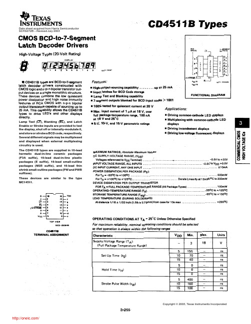
PACKAGING INFORMATIONOrderable Device Status(1)PackageType PackageDrawingPins PackageQtyEco Plan(2)Lead/Ball Finish MSL Peak Temp(3)CD4511BE ACTIVE PDIP N1625Pb-Free(RoHS)CU NIPDAU N/A for Pkg TypeCD4511BEE4ACTIVE PDIP N1625Pb-Free(RoHS)CU NIPDAU N/A for Pkg Type CD4511BF ACTIVE CDIP J161TBD A42N/A for Pkg Type CD4511BF3A ACTIVE CDIP J161TBD A42N/A for Pkg Type CD4511BNSR ACTIVE SO NS162000Green(RoHS&no Sb/Br)CU NIPDAU Level-1-260C-UNLIMCD4511BNSRE4ACTIVE SO NS162000Green(RoHS&no Sb/Br)CU NIPDAU Level-1-260C-UNLIMCD4511BNSRG4ACTIVE SO NS162000Green(RoHS&no Sb/Br)CU NIPDAU Level-1-260C-UNLIMCD4511BPW ACTIVE TSSOP PW1690Green(RoHS&no Sb/Br)CU NIPDAU Level-1-260C-UNLIMCD4511BPWE4ACTIVE TSSOP PW1690Green(RoHS&no Sb/Br)CU NIPDAU Level-1-260C-UNLIMCD4511BPWG4ACTIVE TSSOP PW1690Green(RoHS&no Sb/Br)CU NIPDAU Level-1-260C-UNLIMCD4511BPWR ACTIVE TSSOP PW162000Green(RoHS&no Sb/Br)CU NIPDAU Level-1-260C-UNLIMCD4511BPWRE4ACTIVE TSSOP PW162000Green(RoHS&no Sb/Br)CU NIPDAU Level-1-260C-UNLIMCD4511BPWRG4ACTIVE TSSOP PW162000Green(RoHS&no Sb/Br)CU NIPDAU Level-1-260C-UNLIM(1)The marketing status values are defined as follows:ACTIVE:Product device recommended for new designs.LIFEBUY:TI has announced that the device will be discontinued,and a lifetime-buy period is in effect.NRND:Not recommended for new designs.Device is in production to support existing customers,but TI does not recommend using this part in a new design.PREVIEW:Device has been announced but is not in production.Samples may or may not be available.OBSOLETE:TI has discontinued the production of the device.(2)Eco Plan-The planned eco-friendly classification:Pb-Free(RoHS),Pb-Free(RoHS Exempt),or Green(RoHS&no Sb/Br)-please check /productcontent for the latest availability information and additional product content details.TBD:The Pb-Free/Green conversion plan has not been defined.Pb-Free(RoHS):TI's terms"Lead-Free"or"Pb-Free"mean semiconductor products that are compatible with the current RoHS requirements for all6substances,including the requirement that lead not exceed0.1%by weight in homogeneous materials.Where designed to be soldered at high temperatures,TI Pb-Free products are suitable for use in specified lead-free processes.Pb-Free(RoHS Exempt):This component has a RoHS exemption for either1)lead-based flip-chip solder bumps used between the die and package,or2)lead-based die adhesive used between the die and leadframe.The component is otherwise considered Pb-Free(RoHS compatible)as defined above.Green(RoHS&no Sb/Br):TI defines"Green"to mean Pb-Free(RoHS compatible),and free of Bromine(Br)and Antimony(Sb)based flame retardants(Br or Sb do not exceed0.1%by weight in homogeneous material)(3)MSL,Peak Temp.--The Moisture Sensitivity Level rating according to the JEDEC industry standard classifications,and peak solder temperature.Important Information and Disclaimer:The information provided on this page represents TI's knowledge and belief as of the date that it is provided.TI bases its knowledge and belief on information provided by third parties,and makes no representation or warranty as to the accuracy of such information.Efforts are underway to better integrate information from third parties.TI has taken and continues to take reasonable steps to provide representative and accurate information but may not have conducted destructive testing or chemical analysis on incoming materials and chemicals.TI and TI suppliers consider certain information to be proprietary,and thus CAS numbers and other limited information may not be available for release.In no event shall TI's liability arising out of such information exceed the total purchase price of the TI part(s)at issue in this document sold by TI to Customer on an annual basis.TAPE AND REEL INFORMATION*All dimensions are nominalDevicePackage Type Package Drawing Pins SPQReel Diameter (mm)Reel Width W1(mm)A0(mm)B0(mm)K0(mm)P1(mm)W (mm)Pin1Quadrant CD4511BNSR SO NS 162000330.016.48.210.5 2.512.016.0Q1CD4511BPWRTSSOPPW162000330.012.46.95.61.68.012.0Q1*All dimensions are nominalDevice Package Type Package Drawing Pins SPQ Length(mm)Width(mm)Height(mm) CD4511BNSR SO NS162000367.0367.038.0CD4511BPWR TSSOP PW162000367.0367.035.0分销商库存信息:TICD4511BNSR CD4511BPWR CD4511BECD4511BPWRE4CD4511BPWRG4CD4511BNSRE4 CD4511BNSRG4CD4511BEE4CD4511BPW CD4511BPWE4CD4511BPWG4。
S40B资料
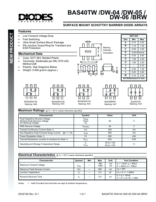
Mechanical Data
· · · · Case: SOT-363, Molded Plastic Terminals: Solderable per MIL-STD-202, Method 208 Polarity: See Diagrams Below Weight: 0.006 grams (approx.)
SOT-363
A
Dim A Marking Indicates B C Orientation B C D E G
Min 0.10 1.15 2.00 0.30 1.80 1.80 ¾ 0.90 0.25 0.10
Max 0.30 1.35 2.20 0.40 2.20 2.20 0.10 1.00 0.40 0.25
1. Valid Provided that terminals are kept at ambient temperature.
DS30156 Rev. D-1
1 of 1
BAS40TW /DW-04 /DW-05 /DW-06 /BRW
Electrical Characteristics
Characteristic Maximum Forward Voltage Maximum Peak Reverse Current Junction Capacitance Reverse Recovery Time Notes:
@ TA = 25°C unless otherwise specified Symbol VFM IRM Cj trr Min ¾ ¾ ¾ ¾ Max 380 1000 200 5.0 5.0 Unit mV mV nA pF ns Test Condition IF = 1.0mA, tp < 300ms IF = 40mA, tp < 300ms VR = 30V VR = 0, f = 1.0MHz IF = IR = 10mA, Irr = 0.1 x IR, RL = 100W
G751中文资料
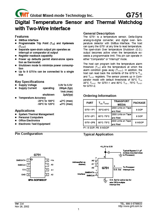
with Two-Wire Interface FeaturesSMBus interfaceProgrammable Trip Point (T OS) and Hysteresis (T HYST)Separate open-drain output pin operates as interrupt or comparator at outputRegister readback capabilityPower up defaults permit stand-alone opera-tion as thermostatShutdown mode to minimize power consump-tionUp to 8 G751s can be connected to a single busKey SpecificationsSupply Voltage 3.0V to 5.5V Supply Current operating 280µA (typ)1mA (max)shutdown 2µA(typ) Temperature Accuracy-25°C to 100°C ±2°C (max)-55°C to 125°C ±3°C (max) ApplicationsSystem Thermal ManagementPersonal ComputersOffice ElectronicsElectronic Test Equipment General DescriptionThe G751 is a temperature sensor, Delta-Sigma analog-to-digital converter, and digital over- tem-perature detector with SMBus interface. The host can query the G751 at any time to read temperature. The open-drain Over temperature Shutdown (O.S.) output becomes active when the temperature ex-ceeds a programmable limit. This pin can operate in either “Comparator” or “Interrupt” mode.The host can program both the temperature alarm threshold (T OS) and the temperature at which the alarm condition goes away (T HYST). In addition, the host can read back the contents of the G751’s T OS and T HYST registers. The sensor powers up in Com-parator mode with default thresholds of 50°C T OS 45°C T HYST. for G751-1 and 80°C T OS , 75°C T HYST for G751-2.Ordering InformationPART T OS T HYSTTRANSPORTMEDIAPACKAGE G751-1P1 50°C/45°C2500 Units on Tapeand Reel8 SOPG751-2P1 80°C/75°C2500 Units on Tapeand Reel8 SOPG751-2P8 80°C/75°C2500 Units on Tapeand Reel8 MSOP P1: 8 SOP; P8: 8 MSOPTypical ApplicationSMBDATA8Pin SOP/MSOP +Vs A0 A1 A2SMBCLKGND Address(Set asInterfaceinterrupt line desired)A0A1A2Supply Voltage………….…………………-0.3V to 6.5V Voltage at any Pin……………….…-0.3V to +Vs +0.3V Input Current at any Pin…………………………….5mA Package Input Current…………………………….20mA O.S. Output Sink Current………………………….10mA O.S. Output Voltage…………………….…………..6.5V Storage Temperature…………………-65°C to +150°C Soldering Information, Lead TemperatureSOP PackageVapor Phase (60 seconds)……………………….215°C Infrared (15 seconds)……………………………..220°C ESD SusceptibilityHuman Body Model (2000V)Machine Model……………………………………...200V Specified Temperature Range…………….T MIN to T MAX-55°Cto+125°C Supply Voltage Range (+Vs)…………..+3.0V to +5.5VTemperature-to-Digital Converter CharacteristicsUnless otherwise noted, these specifications apply for +Vs=+3.3v Vdc. Boldface limits apply for T A=T J=T MIN toT MAX; all other limits T A=T J= +25°C, unless otherwise noted.PARAMETER CONDITIONSTYPICALLIMITSUNITSAccuracy TA=-25°C to +100°CTA=-55°C to +125°C±2.0±3.0 °C (max)Resolution9BitsTemperature Conversion Time 100 MsQuiescent Current SMBus InactiveSMBus ActiveShutdown Mode0.2511.0MamA (max)µAO.S. Output Saturation Voltage I OUT = 4.0mA 0.8 V (max)O.S. Delay 16Conversions (min)Conversions (max)T OS Default Temperature G751-1/G751-2 50/80 °C T HYST Default Temperature G751-1/G751-2 45/75 °CBlock DiagramA0SMBDATAA1A2SMBCLKDigital DC CharacteristicsUnless otherwise noted, these specifications apply for +Vs=+3.3 Vdc. Boldface limits apply for T A =T J =T MIN to T MAX ; all other limits T A =T J =+25°C, unless otherwise noted. SYMBOL PARAMETER CONDITIONS TYPICAL LIMITS UNITSV IN (1) Logical “1” Input Voltage +Vs × 0.7 +Vs + 0.5 V (min) V (max) V IN (0) Logical “0” Input Voltage-0.3 +Vs ×0.3V (min) V (max) I IN (1) Logical “1”Intput Current V IN =5V 0.005 1.0 µA I IN (0) Logical “0”Intput Current V IN =0V -0.005 -1.0µA C IN All Digital Inputs20 PF I OH High Level Output Current V OH =5V 100 µA (max) V OL Low Level Output Voltage I OL =3ma 0.4 V (max) t OFOutput Fall TimeC L =400pF,I O =3ma 250ns (max)SMBus Digital Switching CharacteristicsUnless otherwise noted, these specifications apply for +Vs = +3.3 Vdc and C L (load capacitance) on output lines = 80pF unless otherwise specified. Boldface limits apply for T A = T J = T MIN to T MAX ; all other limits T A = T J = +25°C, unless otherwise noted.The switching characteristics of the G751 fully meet or exceed the published specifications of the SMBus. The following parameters are the timing relationships between SMBCLK and SMBDATA signals related to the G751. They are not the SMBus specifications.SYMBOL PARAMETER CONDITIONS TYPICAL LIMITSUNITSt 1 SMBCLK (Clock) Period2.5 µs (min) t 2 Data in Set-Up Time to SMBCLK High 100 ns (min) t 3 Data Out Stable after SMBCLK Low0 ns (min) t 4 SMBDATA Low Set-Up Time to SMBCLK Low (Start Condition) 100 ns (min) t 5SMBDATA High Hold Time after SMBCLK High (Stop Condition)100ns (min)Pin DescriptionPIN LABELFUNCTIONTYPICAL CONNECTION1 SMBDATA SMBus Serial Bi-Directional Data Line From Controller2 SMBCLK SMBus Clock Input From Controller3 O.S. Overtemperature Shutdown Open Drain Output Pull Up Resistor, Controller Interrupt Line4 GND Power Supply GroundGround5,6,7 A0-A2 User-Set SMBus Address Inputs Ground (Low, “0”) or +Vs (High, “1”) 8 +Vs Positive Supply Voltage InputDC Voltage from 3V to 5.5VLogic Electrical CharacteristicsSMBDATASMBDATA SMBCLKData inData outTemperature-to-Digital Transfer Function (Non-linear scale for clarity)Functional DescriptionThe G751 temperature sensor incorporates a band-gap type temperature sensor and 9-bit ADC (Delta-Sigma Analog- to-Digital Converter). The temperature data output of the G751 is available at all times via the SMBus. If a conversion is in pro-gress, it will be stopped and restarted after the read.A digital comparator is also incorporated that com-pares a series of readings, the number of which is user-selectable, to user-programmable setpoint and hysteresis values. The comparator trips the O.S. output line, which is programmable for mode and polarity.O.S. Output, T OS and T HYST LimitsIn Comparator mode the O.S. Output behaves like a thermostat. The output becomes active when tem-perature exceeds the T OS limit, and leaves the active state when the temperature drops below the T HYST limit. In this mode the O.S. output can be used to turn a cooling fan on, initiate an emergency system shutdown, or reduce system clock speed. Shutdown mode does not reset O.S. state in a comparator mode.In interrupt mode exceeding T OS also makes O.S. active but O.S. will remain active indefinitely until reset by reading any register via the SMBus inter-face. Once O.S. has been activated by crossing T OS, then reset, it can activated again only by Tempera-ture going below T HYST. Again, it will remain active indefinitely until being reset by a read. Placing the G751 in shutdown mode also resets the O.S. output. Default ModesG751 always powers up in a known state. G751 power up default conditions are:1. Comparator mode2. T OS set to 50°C for G751-1, to 80°C for G751-23. T HYST set to 45°C for G751-1, to 75°C for G751-24. O.S. active low5. Pointer set to “00”; Temperature RegisterWith these operating conditions G751 can act as a stand-alone thermostat with the above temperature settings. Connection to an SMBus is not required. SMBus InterfaceThe G751 operates as a slave on the SMBus, so the SMBCLK line is an input (no clock is generated bythe G751) and the SMBDATA line is a bi-directional serial data path. According to SMBus specifications,the G751 has a 7-bit slave address. The four most significant bits of the slave address are hard wired inside the G751 and are “1001”. The three least sig-nificant bits of the address are assigned to pinsA2-A0, and are set by connecting these pins to ground for a low, (0); or to +Vs for a high, (1). Therefore, the complete slave address is:1 0 0 1 A2 A1 A0 MSB LSBFigure1 O.S. Output Temperature Response Diagram Temperature Data FormatTemperature data can be read from the Temperature, T OS Set Point, and T HYST Set Point registers; and written to the T OS Set Point, and T HYST Set Point reg-isters. Temperature data is representedby a 9-bit, two’s complement word with an LSB (Least Significant Bit) equal to 0.5°C:DIGITAL OUTPUTTEMPERATUREBINARY HEX+125°C 0 1111 1010 0FAh +25°C 0 0011 0010 032h +0.5°C 0 0000 0001 001h 0°C 0 0000 0000 000h -0.5°C 1 1111 1111 1FFh -25°C 1 1100 1110 1CEh -55°C 1 1001 0010 192hShutdown ModeShutdown mode is enabled by setting the shutdown bit in the Configuration register via the SMBus. Shut-down mode reduces power supply current to 1 µA typical. In interrupt mode O.S. is reset if previously set and is undefined in Compatator mode during shutdown. The SMBus interface remains active. Ac-tivity on the clock and data lines of the SMBus may slightly increase shutdown mode quiescent current. T OS , T HYST , and Configuration registers can be read from and written to in shutdown mode.Fault QueueA fault queue of up to 6 faults is provided to prevent false tripping of O.S. when the G751 is used in noisy environments. The number of faults set in the queue must occur consecutively to set the O.S. output. Comparator/Interrupt ModeAs indicated in the O.S. Output Temperature Re-sponse Diagram, Figure 1, the events that trigger O.S. are identical for either Comparator or Interrupt mode. The most important difference is that in Inter-rupt mode the O.S. will remain set indefinitely once it has been set. To reset O.S. while in Interrupt mode, perform a read from any register in the G751. O.S. OutputThe O.S. output is an open-drain output and does not have an internal pull-up. A ”high” level will not be observed on this pin until pull-up current is provided from some external source, typically a pull-up resis-tor. Choice of resistor value depends on many sys-tem factors but, in general, the pull-up resistor should be as large as possible. This will minimize any errors due to internal heating of the G751. The maximum resistance of the pull up, based on G751 specification for High Level Output Current, to pro-vide a 2V high level, is 30k Ω.O.S. PolarityThe O.S. output can be programmed via the con-figuration register to be either active low (default mode), or active high. In active low mode the O.S. output goes low when triggered exactly as shown on the O.S. Output Temperature Response Diagram, Figure 1. Active high simply inverts the polarity of the O.S. output.T T O ST H Y S TO .S .(C o m p a r a t o r M o d e )O .S .(I n t e r r u p t M o d e )e m p e r a t u S h o w nf o r O .S . s e t f o r a c t i v e l o w .*r e a d a n y r e g i s t e r o r p l a c e d i n s h u t d o w nThere are four data registers in the G751, selected by the Pointer register. At power-up the Pointer is set to “00”; the location for the Temperature Register. The Pointer register latches whatever the last loca-tion it was set to. In Interrupt Mode, a read from the G751, or placing the device in shutdown mode, re-sets the O.S. output. All registers are read and write, except the Temperature register which is read only. A write to the G751 will always include the address byte and the Pointer byte. A write to the Configura-tion register requires one data byte, and the T OS and T HYST registers require two data bytes.Reading the G751 can take place either of two ways: If the location latched in the Pointer is correct (most of the time it is expected that the Pointer will point to Temperature register because it will be the data most frequently read from the G751), then the read can simply consist of an address byte, followed by retrieving the corresponding number of data bytes. If the Pointer needs to be set, than an address byte, pointer byte, repeat start, and another address byte will accomplish a read.The first data byte is the most significant byte with most signification bit first, permitting only as much data as necessary to be read to determine tempera-ture condition. For instance, if the first four bits of the temperature data indicates an overtemperature con-dition, the host processor could immediately take action to remedy the excessive temperatures. At the end of a read, the G751 can accept either Acknowl-edge or No Acknowledge from the Master (No Ac-knowledge is typically used as a signal for the salve that the Master has read its last byte).An inadvertent 8-bit read from a 16-bit register, with the D7 bit low, can cause the G751 to stop in a state where the SDA line is held low as shown in Figure 2. This can prevent any further bus communication until at least 9 additional clock cycles have occurred. Al-ternatively, the master can issue clock cycles until SDA goes high, at which time issuing a “Stop” condi-tion will reset the G751.Figure 2. Inadvertent 8-Bit Read from 16-Bit Register where D7 is ZeroMaster but G751 locks SMBDATA low Master detects the errorSMBCLKSMBDATAIntended Stop byof its ways(Selects which registers will be read from or written to):P7 P6 P5 P4 P3 P2 P1 P00 0 0 0 0 0 RegisterSelectP0-P1 :Register Select:P1 P0 REGISTER0 0 Temperature (Read only) (Power-up default)Configuration(Read/Write)0 1T HYST (Read/Write)1 0T OS (Read/Write)1 1P2-P7 :Must be kept zero.Temperature Register(Read Only):D15 D14 D13 D12 D11 D10 D9 D8 D7 D6 D5 D4 D3 D2 D1 D0MSB Bit 7 Bit 6 Bit 5 Bit 4 Bit 3 Bit 2 Bit 1 LSB X X X X X X XD0-D6 :UndefinedD7-D15 :Temperature Data. One LSB = 0.5°C. Two’s complement format.Configuration Register(Read/Write):D7 D6 D5 D4 D3 D2 D1 D0Cmp/IntShutdownPolarity0 0 0 FaultO.S.QueuePower up default is with all bits “0” (zero).D0 :Shutdown : When set to 1 the G751 goes to low power shutdown mode.D1 :Comparator / Interrupt mode : 0 is Comparator mode, 1 is Interrupt mode.D2 :O.S. Polarity : 0 is active low, 1 is active high. O.S. is an open-drain output under all conditions.D3-D4 :Fault Queue : Number of faults necessary to detect before setting O.S. output to avoid false tripping dueto noise :OFFAULTS D4 D3NUMBER0 0 1 (Power-up default)0 1 21 0 41 1 6D5-D7 :These bits are used for production testing and must be kept zero for normal operation.T HYST and T OS Register(Read/Write):D15 D14 D13 D12 D11 D10 D9 D8 D7 D6 D5 D4 D3 D2 D1 D0MSB Bit 7 Bit 6 Bit 5 Bit 4 Bit 3 Bit 2 Bit 1 LSB X X X X X X XD0-D6 :UndefinedD7-D15 :T HYST Or T OS Trip Temperature Data. Power up default is T OS = 50°C /80°C for G751-1/G751-2, T HYST =45°C /75°C for G751-1/G751-2.StartG751AckStartG751Master NoCondRepeat Ack Ack No Cond StartG751G751CondbyMasterAddress Byte AckbyPointer BytebyG751byMasterAddress Byte AckbyMost Significant Data ByteAckbyAckbyMasterStopbyMasterLeast Significant Data ByteStartby Master Address BytebyG751Most Significant Data BytebyMasterAckbyMasterStopbyMasterLeast Significant Data BytebyMasterAddress Byte AckbyPointer ByteAckbyStopbyMasterS n S A A A S A A A C t o p C o d b y M a s t e rt a r t b y M a s t e rA d d r e s sB y t ec k b y G 751P o i n t e r B y t e c k b y M a s t e r N o A c k b y M a s t e r A d r e s s B y t e919199R e p e a t S t a r t b y M a s t e r D a t a B y t ec k b y G 751t a r t b y M a s t e rA d d r e s sB y t ec k b y G 751P o i n t e r B y t e c k b y M a s t e r c k b y G 751S t o p o n d b y M a s t e rC o n f i g u r a t i o n B y t et o p o n d b y s t e r1(a ) T y p i c a l P o i n t e r S e t f o l l o w e d b y I m m e d i a t e R e a d f r o m C o n f i g u r a t i o n R e g i s t e r(b ) C o n f i g u r a t i o n R e g i s t e r W r i t e(c ) T O S a n d T H Y S T W r i t e8 Pin SOP PackageNote:1. Package body sizes exclude mold flash and gate burrs2. Dimension L is measured in gage plane3. Tolerance 0.10mm unless otherwise specified4. Controlling dimension is millimeter converted inch dimensions are not necessarily exact.DIMENSION IN MM DIMENSION IN INCHSYMBOLMIN. NOM. MAX. MIN. NOM. MAX.A 1.35 1.60 1.75 0.053 0.063 0.069 A1 0.10 ----- 0.25 0.004 ----- 0.010 A2 ----- 1.45 ----- ----- 0.057 -----B 0.33 ----- 0.51 0.013 ----- 0.020C 0.19 ----- 0.25 0.007 ----- 0.010D 4.80 ----- 5.00 0.189----- 0.197 E 3.80 ----- 4.00 0.150 ----- 0.157 e ----- 1.27 ----- ----- 0.050 ----- H 5.80 ----- 6.20 0.228 ----- 0.244 L 0.40 ----- 1.27 0.016 ----- 0.050 y ----- ----- 0.10 ----- ----- 0.004 θ 0º ----- 8º 0º ----- 8ºVer: 2.4Nov 26, 2002TEL: 886-3-5788833 118 Pin MSOP PackageDIMENSION IN MM DIMENSION IN INCHSYMBOLMIN. NOM. MAX. MIN. NOM. MAX.A ----- ----- 1.10 ----- ----- 0.043 A1 0.05 ----- 0.15 0.002 ----- 0.006A2 0.81 0.86 0.91 0.032 0.034 0.036 b 0.25 ----- 0.40 0.008----- 0.012b1 0.25 0.30 0.35 0.010 0.012 0.014 c 0.13 ----- 0.23 0.005 0.009 c1 0.13 0.15 0.18 0.005 0.006 0.007 D 2.90 3.00 3.10 0.114 0.118 0.122 E1 2.90 3.00 3.10 0.1140.118 0.122 e 0.65 BSC 0.026 BSC E 4.90 BSC 0.193 BSC L 0.445 0.55 0.648 0.0175 0.0217 0.0255 θ1 0° ----- 6° 0° ----- 6° θ2 12 REF 12 REF θ3 12 REF 12 REF R 0.09 ----- ----- 0.004 ----- ----- R1 0.09 ----- ----- 0.004 ----- ----- JEDEC MO-187AATaping SpecificationGMT Inc. does not assume any responsibility for use of any circuitry described, no circuit patent licenses are implied and GMT Inc. reserves the right at any time without notice to change said circuitry and specifications.Typical SOP/MSOP Package OrientationC b1E18E1DETAIL “A”Leb DA2AA1SEATING PLANEbWITH PLATINGBASE METALc1cθ1GAUGE PLANE0.25RR1Lθ3θ2元器件交易网。
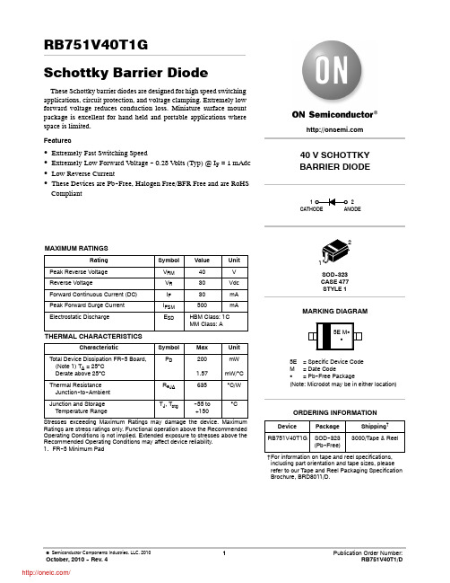
RB751S40T1G中文资料
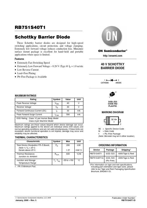
RB751S40T1Schottky Barrier DiodeThese Schottky barrier diodes are designed for high−speed switching applications, circuit protection, and voltage clamping. Extremely low forward voltage reduces conduction loss. Miniature surface mount package is excellent for hand−held and portable applications where space is limited.Features•Extremely Fast Switching Speed•Extremely Low Forward V oltage − 0.28 V (Typ) @ I F = 1.0 mAdc •Low Reverse Current•Lead−Free Plating•Pb−Free Package is AvailableMAXIMUM RATINGSRating Symbol Value Unit Peak Reverse Voltage V RM40V Reverse Voltage V R30V Forward Continuous Current (DC)I F30mA Peak Forward Surge Current I FSM500mA ESD Rating:Class 1C per Human Body ModelClass A per Machine ModelMaximum ratings are those values beyond which device damage can occur. Maximum ratings applied to the device are individual stress limit values (not normal operating conditions) and are not valid simultaneously. If these limits are exceeded, device functional operation is not implied, damage may occur and reliability may be affected.THERMAL CHARACTERISTICSCharacteristic Symbol Max Unit Total Device Dissipation FR−5 Board,(Note 1) T A = 25°CDerate above 25°C P D2001.57mWmW/°CThermal Resistance, Junction−to−Ambient Rq JA635°C/WJunction and StorageTemperature RangeT J, T stg−55 to +150°C 1.FR−5 Minimum Pad.Device Package Shipping†ORDERING INFORMATIONRB751S40T1SOD−5234000/Tape & Reel RB751S40T1G SOD−523(Pb−Free)4000/Tape & Reel†For information on tape and reel specifications, including part orientation and tape sizes, please refer to our Tape and Reel Packaging Specification Brochure, BRD8011/D.ELECTRICAL CHARACTERISTICS (T A = 25°C unless otherwise noted)CharacteristicSymbol Min Typ Max Unit Reverse Breakdown Voltage (I R = 10 m A)V (BR)R 30−−V Total Capacitance(V R = 1.0 V, f = 1.0 MHz)C T − 2.0 2.5pF Reverse Leakage (V R = 30 V)I R −300500nAdc Forward Voltage (I F = 1.0 mAdc)V F−0.280.37Vdc101.00.1V R , REVERSE VOLTAGE (VOLTS)I F , F O R W A R D C U R R E N T (m A )Figure 3. Typical CapacitancePACKAGE DIMENSIONSSOD−523CASE 502−01ISSUE BNOTES:1.DIMENSIONING AND TOLERANCING PER ANSI Y14.5M,1982.2.CONTROLLING DIMENSION: MILLIMETER.3.MAXIMUM LEAD THICKNESS INCLUDES LEAD FINISHTHICKNESS. MINIMUM LEAD THICKNESS IS THE MINIMUM THICKNESS OF BASE MATERIAL.DIMMIN NOM MAX MILLIMETERS A 1.10 1.20 1.30B 0.700.800.90C 0.500.600.70D 0.250.300.35J 0.070.140.20K 0.150.200.25S 1.50 1.60 1.700.0430.0470.0510.0280.0320.0350.0200.0240.0280.0100.0120.0140.00280.00550.00790.0060.0080.0100.0590.0630.067MIN NOM MAX INCHES*For additional information on our Pb−Free strategy and solderingdetails, please download the ON Semiconductor Soldering and Mounting Techniques Reference Manual, SOLDERRM/D.SOLDERING FOOTPRINT*ǒmm inchesǓSCALE 10:1ON Semiconductor and are registered trademarks of Semiconductor Components Industries, LLC (SCILLC). SCILLC reserves the right to make changes without further notice to any products herein. SCILLC makes no warranty, representation or guarantee regarding the suitability of its products for any particular purpose, nor does SCILLC assume any liability arising out of the application or use of any product or circuit, and specifically disclaims any and all liability, including without limitation special, consequential or incidental damages.“Typical” parameters which may be provided in SCILLC data sheets and/or specifications can and do vary in different applications and actual performance may vary over time. All operating parameters, including “Typicals” must be validated for each customer application by customer’s technical experts. SCILLC does not convey any license under its patent rights nor the rights of others. SCILLC products are not designed, intended, or authorized for use as components in systems intended for surgical implant into the body, or other applications intended to support or sustain life, or for any other application in which the failure of the SCILLC product could create a situation where personal injury or death may occur. Should Buyer purchase or use SCILLC products for any such unintended or unauthorized application, Buyer shall indemnify and hold SCILLC and its officers, employees, subsidiaries, affiliates, and distributors harmless against all claims, costs, damages, and expenses, and reasonable attorney fees arising out of, directly or indirectly, any claim of personal injury or death associated with such unintended or unauthorized use, even if such claim alleges that SCILLC was negligent regarding the design or manufacture of the part. SCILLC is an Equal Opportunity/Affirmative Action Employer. This literature is subject to all applicable copyright laws and is not for resale in any manner.PUBLICATION ORDERING INFORMATION。
LRB751V-40T1中文资料
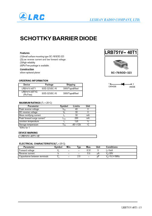
10
1 Ta = 25oC 100n Ta = -25oC Typ. pulse measurement 5 10 15 20 25 30 REVERSE VOLTAGE : VR (V) 35
10n
1n 0
Fig. 2 Reverse characteristics
DEVICE MARKING
LRB751V-40T1= 5E
ELECTRICAL CHARACTERISTICS(TA = 25°C)
Parameter Forward voltage Reverse current Capacitance between terminals Symbol VF IR CT Min. Typ 2.0 Max. 0.37 0.5 Unit V µA pF Conditions IF=1mA VR=30V VR=1V,f=1MHz
LRB751V-40T1–1/3
元器件交易网
LESHAN RADIO COMPANY, LTD.
LRB751V-40T1 Electrical characteristic curves(TA = 25°C)
1000m Typ. pulse measurement 100m 10m 1m 100 10 1
LRB751V- 40T1
Construction
silicon epitaxial planar
SC-76/SOD-323
ORDERING INFORMATION
Device LRB751V-40T1 LRB751V-40T1G (Pb-Free) Package SOD-323/SC-76 SOD-323/SC-76 Shipping 3000/Tape&Reel 3000/Tape&Reel
FOSAN富信电子 二级管 RB751S-40-产品规格书
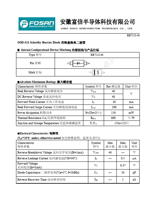
安徽富信半导体科技有限公司ANHUI FOSAN SEMICONDUCTOR TECHNOLOGY CO.,LTD.RB751S-40SOD-523Schottky Barrier Diode 肖特基势垒二极管▉Internal Configuration&DeviceMarking 内部结构与产品打标Type 型号RB751S-40Pin 管脚Mark 打标▉AbsoluteMaximum Ratings 最大额定值Characteristic 特性参数Symbol 符号Rat 额定值Unit 单位Peak Reverse V oltage 反向峰值电压V RM 40V DC Reverse Voltage 直流反向电压V R 40Forward Work Current 正向工作电流I O 30mA Peak Forward Surge Current 正向峰值浪涌电流I FSM200mA Power dissipation 耗散功率P D (Ta=25℃)150mW Thermal Resistance J-A 结到环境热阻R θJA 668℃/WJunction and Storage Temperature 结温和储藏温度T J ,T stg-55to+125℃■Electrical Characteristics 电特性(T A =25℃unless otherwise noted 如无特殊说明,温度为25℃)Characteristic 特性参数Symbol 符号Min 最小值Max 最大值Unit 单位Reverse Breakdown Voltage 反向击穿电压(I R =1mA)V (BR)40—V Reverse Leakage Current 反向漏电流(V R =30V)I R —0.5µA Forward V oltage 正向电压(I F =1mA)V F 0.37V Diode Capacitance 二极管电容(V R =1V,f=1MHz)C D—10pF Reverse Recovery Time 反向恢复时间T rr—5nSANHUI FOSAN SEMICONDUCTOR TECHNOLOGY CO.,LTD.RB751S-40■Typical Characteristic Curve典型特性曲线ANHUI FOSAN SEMICONDUCTOR TECHNOLOGY CO.,LTD.RB751S-40■Dimension外形封装尺寸。
RB751CS-40中文资料
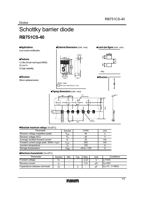
8 7 6 5 4 3 2 1 0 AVE:1.81pF
310
300
290 AVE:304.2mV 280 VF DISPERSION MAP
IR DIቤተ መጻሕፍቲ ባይዱPERSION MAP
Ct DISPERSION MAP
20
30 25 20 15 10 AVE:11.7ns 5 0 IFSM DISRESION MAP trr DISPERSION MAP
10
1 0 5 10 15 20 25 30 35 REVERSE VOLTAGE:VR(V) VR-IR CHARACTERISTICS 40
0.1 0 5 10 15 20 25 30 REVERSE VOLTAGE:VR(V) VR-Ct CHARACTERISTICS
330
1000
10 Ta=25℃ VR=30V n=30pcs 9 Ta=25℃ f=1MHz VR=0V n=10pcs
2/3
元器件交易网
RB751CS-40
Diodes
0.003
0.1
0.1 VR D=t/T VR=20V Tj=125℃
AVERAGE RECTIFIDE FORWARD CURRENT:Io(A)
0.08
AVERAGE RECTIFIED FORWARD CURRENT:Io(A)
DC D=1/2
D=1/2
0.02
Sin(θ=180) 0 0 10 20 30 40 REVERSE VOLTAGE:VR(V) VR-PR CHARACTERISTICS
0 0 25 50 75 100 125
AMBIENT TEMPERATURE:Ta(℃) Derating Curve゙(Io-Ta)
SEL-751A中文 datasheet

{CLOSE} 和 {TRIP} 操作控制 (见图2)用于连接断路器 的合闸和跳闸操作。可设定延时控制,用于开关柜安装 断路器的操作要求。采用该功能可使操作员按下
{CLOSE}或 {TRIP}按钮后,有足够的时间在断路器控 制命令执行前转移到安全地带。
一次重合闸(可选)
SEL-751A在进入锁定状态前,可完成对断路器的一次 重合。应用SELOGIC 控制方程设定SEL-751A实现下列 重合功能:
深圳市中电电力技术有限公司 2
SEL-751A 简介
图1 星型或开口三角电压连接到SEL-751A三相电压输入
电压断线逻辑
SEL-751A 包含电压断线逻辑,可检测单相、两相或三 相电压回路断线。这种专利的电压断线检测逻辑不需设 定,适用于各种应用。
电压断线特性可用于闭锁保护元件,增加在断线时的安 全性。
此外,SEL-751A还支持单电压输入。对于采用单电压 输入的用户,SEL-751A将按照三相电压平衡的假定, 完成所以的保护和测量功能。
用于相故障检测的过电流元件
相和负序过电流元件用于检测相间故障。负序电流不反 映三相负荷电流,从而提供更高的相间故障灵敏性。三 相故障没有显著的负序分量,可通过相过流元件检测。
电压 VA,B,C
星型连接电压输入
电压 VAB,BC,CA
三角形连接电压输入
功率 KW3P,KVAR3P
三相有功和无功
电能 KWh3P, KVARh3P
三相有功和无功电度
功率因数 Factor PF3P
三相功率因数;超前或滞后
序分量 3I2, 3I0, 3V2, 3V0
负序和零序电流和电压
频率 FREQ (Hz)
启动重合闸(如特定的保护跳闸动作) 闭锁重合闸 (如当特定的光隔输入复位时) 延时重合闸(如近端严重故障跳闸后)
RB751V40T1G;RB751V40T1;中文规格书,Datasheet资料
820 +10 V 2k 100 H 0.1 F DUT 50 OUTPUT PULSE GENERATOR 50 INPUT SAMPLING OSCILLOSCOPE 90% VR IR iR(REC) = 1 mA OUTPUT PULSE (IF = IR = 10 mA; measured at iR(REC) = 1 mA) IF 0.1 F tr 10% tp t IF trr t
40 V SCHOTTKY BARRIER DIODE
1 CATHODE
2 ANODE
MAXIMUM RATINGS
Rating Peak Reverse Voltage Reverse Voltage Forward Continuous Current (DC) Peak Forward Surge Current Electrostatic Discharge Symbol VRM VR IF IFSM ESD Value 40 30 30 500 HBM Class: 1C MM Class: A Unit V Vdc mA mA 1
Stresses exceeding Maximum Ratings may damage the device. Maximum Ratings are stress ratings only. Functional operation above the Recommended Operating Conditions is not implied. Extended exposure to stresses above the Recommended Operating Conditions may affect device reliability. 1. FR--5 Minimum Pad
RB751V40中文资料
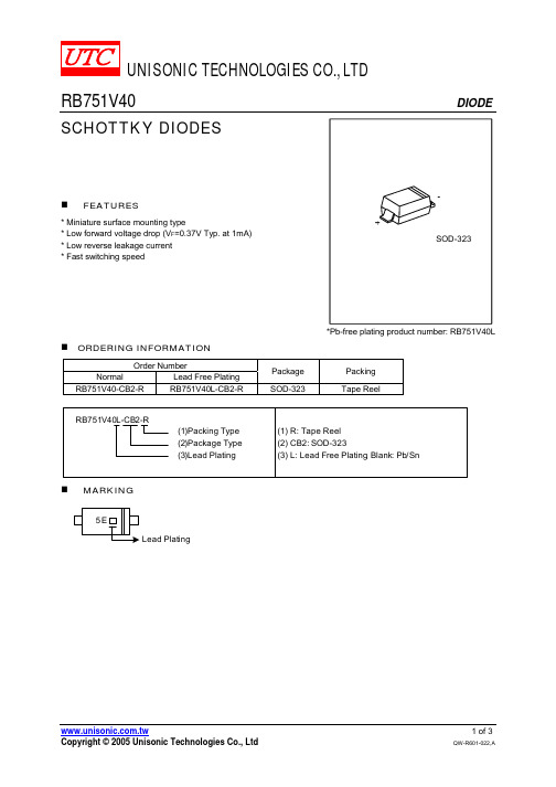
1µ
0
0.2
0.4
0.6
0.8
1.0
1.2
1.4
1.6
1n 0 5 10 15 20 25 30 35 Reverse Voltage, VR (V)
Fonward Voltage, VF (V)
Capacitance Between Terminals Characteristics 100
Capacitance Between Terminals, CT (pF)
DIODE
PARAMETER SYMBOL RATINGS UNIT Peak Reverse Voltage VRM 40 V Maximum Reverse Voltage (DC) VR 30 V Mean Rectifying Current IOUT 30 mA Non-repetitive Peak Forward Surge Current IFSM 200 mA 125 ℃ Junction Temperature TJ ℃ Storage Temperature TSTG -40 ~ +125 Note: Absolute maximum ratings are those values beyond which the device could be permanently damaged. Absolute maximum ratings are stress ratings only and functional device operation is not implied.
50
Ta = 25℃ f = 1MHz
20 10 5
2
1 0 2 4 6 8 10 12 Reverse Voltage, VR (V)
RB751S-40C2中文资料

Small Signal Schottky diodeRB751S-40C2DescriptionPlanar silicon Schottky barrier diode encapsulated in a SOD-523 plastic SMD package.Features•Extremely small surface mounting type.(SC-79/SOD523)•Low reverse current and low forward voltage•High reliabilityApplicationsLow current rectification and high speed switchingSymbol OutlineRB751S-40C2Absolute Maximum Ratings• Maximum TemperaturesStorage Temperature Tstg.................................................................................................... -45~+125°C Junction Temperature Tj.............................................................................................................. +125°C • Maximum V oltages and Currents (Ta=25°C)Peak Reverse V oltage V RM………………………………………………………………………….40 V DC Reverse V oltage V R...................................................................................................................... 30 V Mean Rectifying Current I F........................................................................................................... 30 mA Peak Forward Surge Current I FSM………………………………….. ……………………………………….200 mACharacteristics (Ta=25°C)Characteristic Symbol Condition Min. Typ Max. UnitForward V oltage V F I F1mA - - 370 mV Reverse Leakage Current I R V R 30V - - 0.5 µA Capacitance Between TerminalsC TV R =1V, f=1MHz - 2 - pFCharacteristic CurvesSOD-523 Dimension*: TypicalMillimeters MillimetersDIMMin .Max. DIMMin. Max.A 0.5 0.7 E 0.7 0.9 b p 0.25 0.35 H E 1.5 1.7 c 0.1 0.2 V 0.15(typ) D 1.1 1.3Notes: 1.Maximum lead thickness includes lead finish thickness, and minimum lead thickness is the minimum thickness of base material. 2.If there is any question with packing specification or packing method, please contact your local CYStek sales office.Material:• Lead: 42 Alloy; solder plating• Mold Compound: Epoxy resin family, flammability solid burning class: UL94V-0Important Notice:• All rights are reserved. Reproduction in whole or in part is prohibited without the prior written approval of CYStek. • CYStek reserves the right to make changes to its products without notice.• CYStek semiconductor products are not warranted to be suitable for use in Life-Support Applications, or systems.• CYStek assumes no liability for any consequence of customer product design, infringement of patents, or application assistance.Marking Code :52-lead SOD-523 Plastic Package CYStek Package Code : C2Style : Pin 1. Cathode 2. Anode212 1。
78S40资料
LM78S40Universal Switching Regulator SubsystemGeneral DescriptionThe LM78S40is a monolithic regulator subsystem consisting of all the active building blocks necessary for switching regu-lator systems.The device consists of a temperature com-pensated voltage reference,a duty-cycle controllable oscilla-tor with an active current limit circuit,an error amplifier,high current,high voltage output switch,a power diode and an uncommitted operational amplifier.The device can drive ex-ternal NPN or PNP transistors when currents in excess of 1.5A or voltages in excess of 40V are required.The device can be used for step-down,step-up or inverting switching regulators as well as for series pass regulators.It features wide supply voltage range,low standby power dissipation,high efficiency and low drift.It is useful for any stand-alone,low part count switching system and works extremely well in battery operated systems.Featuresn Step-up,step-down or inverting switching regulators n Output adjustable from 1.25V to 40Vn Peak currents to 1.5A without external transistors n Operation from 2.5V to 40V input n Low standby current drain n 80dB line and load regulationn High gain,high current,independent op amp nPulse width modulation with no double pulsingBlock and Connection DiagramsApril 1998LM78S40Universal Switching Regulator Subsystem©1998National Semiconductor Corporation Ordering InformationPart Number NS Package Temperature Range LM78S40J/883J16A Ceramic DIP−55˚C to+125˚C LM78S40N N16E Molded DIP−40˚C to+125˚C LM78S40CN N16E Molded DIP0˚C to+70˚C2Absolute Maximum Ratings(Note1)If Military/Aerospace specified devices are required, please contact the National Semiconductor Sales Office/ Distributors for availability and specifications.Storage Temperature RangeCeramic DIP−65˚C to+175˚C Molded DIP−65˚C to+150˚C Operating Temperature RangeExtended(LM78S40J)−55˚C to+125˚C Industrial(LM78S40N)−40˚C to+125˚C Commercial(LM78S40CN)0˚C to+70˚C Lead TemperatureCeramic DIP(Soldering,60sec.)300˚C Molded DIP(Soldering,10sec.)265˚C Internal Power Dissipation(Note2)(Note3)16L-Ceramic DIP 1.50W 16L-Molded DIP 1.04W Input Voltage from V IN to GND40V Input Voltage from V+(Op Amp)to GND40V Common Mode Input Range(Comparator and Op Amp)−0.3to V+ Differential Input Voltage(Note4)±30V Output Short CircuitDuration(Op Amp)Continuous Current from V REF10mA Voltage from SwitchCollectors to GND40V Voltage from SwitchEmitters to GND40V Voltage from SwitchCollectors to Emitter40V Voltage from Power Diode to GND40V Reverse Power Diode Voltage40V Current through Power Switch 1.5A Current through Power Diode 1.5A ESD Susceptibility(to be determined)LM78S40Electrical Characteristics(Note5)T A=Operating temperature range,V IN=5.0V,V+(Op Amp)=5.0V,unless otherwise specified.Symbol Parameter Conditions Min Typ Max Units GENERAL CHARACTERISTICSI CC Supply Current V IN=5.0V 1.8 3.5mA(Op Amp Disconnected)V IN=40V 2.3 5.0mAI CC Supply Current V IN=5.0V 4.0mA(Op Amp Connected)V IN=40V 5.5mA REFERENCE SECTIONV REF Reference Voltage I REF=1.0mA Extend−55˚C<T A<+125˚C,Comm0<T A<+70˚C, 1.180 1.245 1.310VIndus−40˚C<T A<+85˚CV R LINE Reference Voltage V IN=3.0V to V IN=40V,0.040.2mV/V Line Regulation I REF=1.0mA,T A=25˚CV R LOAD Reference Voltage I REF=1.0mA to I REF=10mA,0.20.5mV/mA Load Regulation T A=25˚COSCILLATOR SECTIONI CHG Charging Current V IN=5.0V,T A=25˚C2050µAI CHG Charging Current V IN=40V,T A=25˚C2070µAI DISCHG Discharge Current V IN=5.0V,T A=25˚C150250µAI DISCHG Discharge Current V IN=40V,T A=25˚C150350µAV OSC Oscillator Voltage Swing V IN=5.0V,T A=25˚C0.5Vt on/t off Ratio of Charge/ 6.0µs/µs Discharge TimeCURRENT LIMIT SECTIONV CLS Current Limit SenseVoltageT A=25˚C250350mV OUTPUT SWITCH SECTIONV SAT1Output Saturation Voltage1I SW=1.0A(Figure1) 1.1 1.3VV SAT2Output Saturation Voltage2I SW=1.0A(Figure2)0.450.7VLM78S40Electrical Characteristics(Note5)(Continued)T A=Operating temperature range,V IN=5.0V,V+(Op Amp)=5.0V,unless otherwise specified.Symbol Parameter Conditions Min Typ Max Units OUTPUT SWITCH SECTIONh FE Output Transistor CurrentI C=1.0A,V CE=5.0V,T A=25˚C70GainI L Output Leakage Current V O=40V,T A=25˚C10nA POWER DIODEV FD Forward Voltage Drop I D=1.0A 1.25 1.5V I DR Diode Leakage Current V D=40V,T A=25˚C10nA COMPARATORV IO Input Offset Voltage V CM=V REF 1.515mV I IB Input Bias Current V CM=V REF35200nA I IO Input Offset Current V CM=V REF 5.075nA V CM Common Mode VoltageT A=25˚C0V IN–2V RangeV IN=3.0V to40V,T A=25˚C7096dB PSRR Power Supply RejectionRatioOPERATIONAL AMPLIFIERV IO Input Offset Voltage V CM=2.5V 4.015mV I IB Input Bias Current V CM=2.5V30200nA I IO Input Offset Current V CM=2.5V 5.075nA A VS+Voltage Gain+R L=2.0kΩto GND;25250V/mVV O=1.0V to2.5V,T A=25˚CA VS−Voltage Gain−R L=2.0kΩto V+(Op Amp)25250V/mVV O=1.0V to2.5V,T A=25˚CV CM Common Mode VoltageT A=25˚C0V CC−2V RangeCMR Common Mode Rejection V CM=0V to3.0V,T A=25˚C76100dB PSRR Power Supply RejectionV+(Op Amp)=3.0V to40V,T A=25˚C76100dB RatioI O+Output Source Current T A=25˚C75150mA I O−Output Sink Current T A=25˚C1035mA SR Slew Rate T A=25˚C0.6V/µs V OL Output Voltage LOW I L=−5.0mA,T A=25˚C 1.0V V OH Output Voltage High I L=50mA,T A=25˚C V+(Op VAmp)−3VNote1:Absolute Maximum Ratings indicate limits beyond which damage to the device may occur.Electrical specifications do not apply when ordering the device beyond its rated operating conditions.Note2:T J Max=150˚C for the Molded DIP,and175˚C for the Ceramic DIP.Note3:Ratings apply to ambient temperature at25˚C.Above this temperature,derate the16L-Ceramic DIP at10mW/˚C,and the16L-Molded DIP at8.3mW/˚C.Note4:For supply voltages less than30V,the absolute maximum voltage is equal to the supply voltage.Note5:A military RETS specification is available on request.At the time of printing,the LM78S40RETS specification complied with the Min and Max limits in this table.The LM78S40J may also be procured as a Standard Military Drawing.4Typical Performance CharacteristicsDesign FormulasCharacteristic Step-Down Step-Up Inverting UnitsFunctional DescriptionSWITCHING FREQUENCY CONTROLThe LM78S40is a variable frequency,variable duty cycle device.The initial switching frequency is set by the timing capacitor.(Oscillator frequency is set by a single external capacitor and may be varied over a range of100Hz to 100kHz).The initial duty cycle is6:1.This switching fre-quency and duty cycle can be modified by two mechanisms—the current limit circuitry(I pk sense)and the comparator.The comparator modifies the OFF time.When the output voltage is correct,the comparator output is in the HIGH state and has no effect on the circuit operation.If the out-put voltage is too high then the comparator output goes LOW.In the LOW state the comparator inhibits the turn-on of the output stage switching transistors.As long as the comparator is LOW the system is in OFF time.As the out-put current rises the OFF time decreases.As the output current nears its maximum the OFF time approaches its minimum value.The comparator can inhibit several ON cycles,one ON cycle or any portion of an ON cycle.Once the ON cycle has begun the comparator cannot inhibit un-til the beginning of the next ON cycle.The current limit modifies the ON time.The current limit is activated when a300mV potential appears between lead 13(V CC)and lead14(I pk).This potential is intended to re-sult when designed for peak current flows through R SC. When the peak current is reached the current limit is turned on.The current limit circuitry provides for a quick end to ON time and the immediate start of OFF time. Generally the oscillator is free running but the current limit action tends to reset the timing cycle.Increasing load results in more current limited ON time and less OFF time.The switching frequency increases with load current.USING THE INTERNAL REFERENCE,DIODE,AND SWITCHThe internal1.245V reference(pin8)must be bypassed, with0.1µF directly to the ground pin(pin11)of the LM78S40,to assure its stability.V FD is the forward voltage drop across the internal power diode.It is listed on the data sheet as1.25V typical,1.5V maximum.If an external diode is used,then its own for-ward voltage drop must be used for V FD.V SAT is the voltage across the switch element(output tran-sistors Q1and Q2)when the switch is closed or ON.This is listed on the data sheet as Output Saturation Voltage.“Output saturation voltage1”is defined as the switching element voltage for Q2and Q1in the Darlington configu-ration with collectors tied together.This applies to Figure 1,the step down mode.“Output saturation voltage2”is the switching element volt-age for Q1only when used as a transistor switch.This ap-plies to Figure2,the step up mode.For the inverting mode,Figure3,the saturation voltage of the external transistor should be used for V SAT.Typical ApplicationsCharacteristic Condition TypicalValue Output Voltage I O=200mA10V Line Regulation20V≤V I≤30V 1.5mV Load Regulation 5.0mA≤I O 3.0mVI O≤300mAMax Output Current V O=9.5V500mA Output Ripple I O=200mA50mV Efficiency I O=200mA74% Standby Current I O=200mA 2.8mA Note7:For I O≥200mA use external diode to limit on-chip power dissipation.DS010057-3 FIGURE1.Typical Step-Down Regulator andOperational Performance(T A=25˚C)6Typical Applications(Continued)Characteristic Condition TypicalValue Output Voltage I O=50mA25V Line Regulation 5.0V≤V I≤15V 4.0mV Load Regulation 5.0mA≤I O 2.0mVI O≤100mAMax Output Current V O=23.75V160mA Output Ripple I O=50mA30mV Efficiency I O=50mA79% Standby Current I O=50mA 2.6mACharacteristic Condition TypicalValue Output Voltage I O=100mA−15V Line Regulation8.0V≤V I≤18V 5.0mV Load Regulation 5.0mA≤I O 3.0mVI O≤150mAMax Output Current V O=14.25V160mA Output Ripple I O=100mA20mV Efficiency I O=100mA70% Standby Current I O=100mA 2.3mADS010057-4FIGURE2.Typical Step-Up Regulator and Operational Performance(T A=25˚C)DS010057-5FIGURE3.Typical Inverting Regulator andOperational Performance(T A=25˚C)Typical Applications(Continued)8Physical Dimensions inches(millimeters)unless otherwise noted16-Lead Molded Dual-In-Line Package(N)Order Number LM78S40N or LM78S40CNNS Package Number N16ALIFE SUPPORT POLICYNATIONAL’S PRODUCTS ARE NOT AUTHORIZED FOR USE AS CRITICAL COMPONENTS IN LIFE SUPPORT DE-VICES OR SYSTEMS WITHOUT THE EXPRESS WRITTEN APPROVAL OF THE PRESIDENT OF NATIONAL SEMI-CONDUCTOR CORPORATION.As used herein:1.Life support devices or systems are devices or sys-tems which,(a)are intended for surgical implant intothe body,or (b)support or sustain life,and whose fail-ure to perform when properly used in accordancewith instructions for use provided in the labeling,can be reasonably expected to result in a significant injury to the user.2.A critical component in any component of a life support device or system whose failure to perform can be rea-sonably expected to cause the failure of the life support device or system,or to affect its safety or effectiveness.National Semiconductor Corporation AmericasTel:1-800-272-9959Fax:1-800-737-7018Email:support@National Semiconductor EuropeFax:+49(0)180-5308586Email:europe.support@Deutsch Tel:+49(0)180-5308585English Tel:+49(0)180-5327832Français Tel:+49(0)180-5329358Italiano Tel:+49(0)180-5341680National Semiconductor Asia Pacific Customer Response Group Tel:65-2544466Fax:65-2504466Email:sea.support@National Semiconductor Japan Ltd.Tel:81-3-5620-6175Fax:81-3-5620-6179L M 78S 40U n i v e r s a l S w i t c h i n g R e g u l a t o r S u b s y s t e mNational does not assume any responsibility for use of any circuitry described,no circuit patent licenses are implied and National reserves the right at any time without notice to change said circuitry and specifications.。
NCV7513BFTR2G;中文规格书,Datasheet资料

DRN0 – DRN5
Analog Drain Feedback: Internally Clamped
GAT0 – GAT5
Analog Gate Drive: 5.0 V Compliant
ENA1, ENA2
Digital Master Enable Inputs: 3.3 V/5.0 V (TTL) Compatible
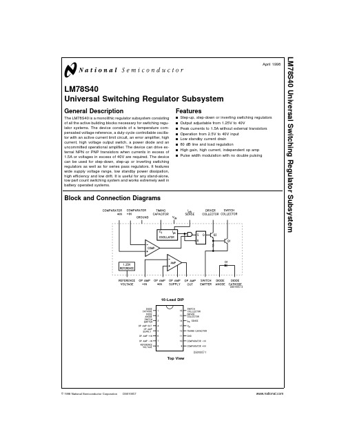
Fault information for each channel is 2−bit encoded by fault type and is available through SPI communication. Fault recovery operation for each channel is programmable and may be selected for latch−off or automatic retry.
• These are Pb−Free Devices*
Benefits
• Scalable to Load by Choice of External MOSFET
*For additional information on our Pb−Free strategy and soldering details, please download the ON Semiconductor Soldering and Mounting Techniques Reference Manual, SOLDERRM/D.
IN0 – IN5
Digital Parallel Input: 3.3 V/5.0 V (TTL) Compatible
CSB
Digital Chip Select Input: 3.3 V/5.0 V (TTL) Compatible
on semi元器件rb751s40的命名方法
on semi元器件rb751s40的命名方法标题:深度解析on semi元器件rb751s40的命名方法在现代科技高速发展的时代,电子元器件在各行各业中扮演着至关重要的角色。
而在这些元器件中,on semi元器件rb751s40作为一种特定型号的器件,其命名方法更是引人注目。
在本文中,将对on semi元器件rb751s40的命名方法进行深入探讨,帮助读者更加全面地了解这一主题。
1. rb751s40的命名解析当我们看到on semi元器件rb751s40的型号时,可能会觉得有些晦涩难懂。
事实上,这个型号是由若干部分构成的,而每一部分都代表着特定的含义。
rb751s40中的“rb”代表着这是一种整流器,而“751”则表示了器件的特定型号。
而最后的“s40”则是指器件的工作电压或其他特性。
通过这种命名方法,我们可以快速了解到这个元器件的基本属性和特点。
2. rb751s40的功能和应用领域针对on semi元器件rb751s40的功能和应用领域,我们可以发现它主要用于电子设备中的功率整流和电源管理。
由于其稳定可靠的特性,它在各种电子产品中都有着广泛的应用,包括手机、笔记本电脑、数码相机等等。
这些应用领域也进一步展示了rb751s40的重要性和价值。
3. rb751s40的命名方法对比相比于其他类型的元器件,on semi rb751s40的命名方法可能会让人觉得更加复杂和专业。
但实际上,这种命名方法能够更加直观地传达出元器件的特性和用途。
相比之下,一些其他型号的命名方法可能显得更加晦涩,需要进一步的解析才能理解其含义。
rb751s40的命名方法在某种程度上也体现了其简洁和明了。
4. 个人观点和总结从个人角度来看,rb751s40的命名方法虽然可能会给初学者带来一定的困扰,但它所蕴含的丰富信息和直观性也使得我们能够更快速地理解和应用该元器件。
rb751s40所代表的整流器类型和特定型号也让它在市场上有着重要的地位,对于电子产业的发展也起到了至关重要的作用。
RB751S40,115;RB751V40,115;RB751CS40,315;中文规格书,Datasheet资料

Package SOD882 SOD523 SOD323
Description 2 mm pitch, 8 mm tape and reel 2 mm pitch, 8 mm tape and reel 4 mm pitch, 8 mm tape and reel 4 mm pitch, 8 mm tape and reel
junction temperature ambient temperature storage temperature
Device mounted on an FR4 Printed-Circuit Board (PCB), single-sided copper, tin-plated and standard footprint. Reflow soldering is the only recommended soldering method.
Product data sheet
Rev. 01 — 21 May 2007
3 of 10
/
NXP Semiconductors
RB751 series
Schottky barrier single diodes
102
IF (mA)
mlc361
103 IR (µA)
[1]
1 1
001aab540
2
sym001
2
[1]
The marking bar indicates the cathode.
3. Ordering information
Table 4. Ordering information Package Name RB751CS40 RB751S40 RB751V40 SC-79 SC-76 Description leadless ultra small plastic package; 2 terminals; body 1.0 × 0.6 × 0.5 mm plastic surface-mounted package; 2 leads plastic surface-mounted package; 2 leads Version SOD882 SOD523 SOD323 Type number
RB751S-40LP-TP;中文规格书,Datasheet资料

RB 751S -40L P30 mASchottky Rectifier40 VoltsFeatures• Small surface mounting typeMicro Commercial Componentsomp onents 20736 Marilla Street Chatsworth! "# $ % ! "#Symbol Rating Rating Unit V R DC Reverse Voltage 30V I O Mean Rectifying Current 30 mA I FSM Peak Forward Surge Current* 150 m A T J Junction Temperature 125 кT STG Storage Temperature -40 to +125 кElectrical Characteristics @ 25O C Unless Otherwise SpecifiedSymbolParameter Min Typ Max UnitsV F Forward Voltage(I F =1mAdc) --- --- 0.37 VdcI RReverse Current(V R =30Vdc)--- --- 0.5 uAdc• Lead Free Finish/RoHS Compliant ("P" Suffix designates RoHS Compliant. See ordering information)• Marking: 5V RM Peak Reverse Voltage 40 V • Epoxy meets UL 94 V-0 flammability rating • Moisture Sensitivity Level 1Micro Commercial Components Typical CharacteristicsMicro Commercial ComponentsOrdering Information :Device PackingPart Number-TP Tape&Reel: 10Kpcs/Reel***IMPORTANT NOTICE***Micro Commercial Components Corp. reserve s the right to make changes without further notice to any product herein to make corrections, modifications , enhancements , improvements , or other changes . Micro Commercial Components Corp . does not assume any liability arising out of the application or use of any product described herein; neither does it convey any license under its patent rights ,nor the rights of others . The user of products in such applications shall assume all risks of such use and will agree to hold Micro Commercial Components Corp . and all the companies whose products are represented on our website, harmless against all damages.***LIFE SUPPORT***MCC's products are not authorized for use as critical components in life support devices or systems without the express writtenapproval of Micro Commercial Components Corporation.***CUSTOMER AWARENESS***Counterfeiting of semiconductor parts is a growing problem in the industry. Micro Commercial Components (MCC) is taking strong measures to protect ourselves and our customers from the proliferation of counterfeit parts. MCC strongly encourages customers to purchase MCC parts either directly from MCC or from Authorized MCC Distributors who are listed by country on our web page cited below. Products customers buy either from MCC directly or from Authorized MCC Distributors are genuine parts, have full traceability, meet MCC's quality standards for handling and storage. MCC will not provide any warranty coverage or other assistance for parts bought from Unauthorized Sources. MCC is committed to combat this global problem and encourage our customers to do their part in stopping this practice by buying direct or from authorized distributors./分销商库存信息: MICRO-COMMERICAL-CO RB751S-40LP-TP。
- 1、下载文档前请自行甄别文档内容的完整性,平台不提供额外的编辑、内容补充、找答案等附加服务。
- 2、"仅部分预览"的文档,不可在线预览部分如存在完整性等问题,可反馈申请退款(可完整预览的文档不适用该条件!)。
- 3、如文档侵犯您的权益,请联系客服反馈,我们会尽快为您处理(人工客服工作时间:9:00-18:30)。
2. A critical component in any component of a life support, device, or system whose failure to perform can be reasonably expected to cause the failure of the life support device or system, or to affect its safety or effectiveness.
Units
VRRM
Maximum Repetitive Reverse Voltage
40
V
IF(AV)
Average Rectified Forward Current
30
mA
IFSM
Non-Repetitive Peak Forward Current
500
mA
TJ
Operating Junction Temperature Range
TRADEMARKS
The following includes registered and unregistered trademarks and service marks, owned by Fairchild Semiconductor and/or its global subsidiaries, and is not
®*
The Power Franchise®
TinyBoost¥ TinyBuck¥ TinyCalc¥ TinyLogic® TINYOPTO¥ TinyPower¥ TinyPWM¥ TinyWire¥ TriFault Detect¥ TRUECURRENT¥* PSerDes¥
UHC® Ultra FRFET¥ UniFET¥ VCX¥ VisualMax¥ XS™
ANTI-COUNTERFEITING POLICY
Fairchild Semiconductor Corporation's Anti-Counterfeiting Policy. Fairchild's Anti-Counterfeiting Policy is also stated on our external website, , under Sales Support.
intended to be an exhaustive list of all such trademarks.
AccuPower¥ Auto-SPM¥ Build it Now¥ CorePLUS¥ CorePOWER¥ CROSSVOLT¥ CTL™ Current Transfer Logic™ EcoSPARK® EfficentMax™ EZSWITCH™*
Value 200 500
Units mW °C/W
Electrical Characteristics TA=25°C unless otherwise noted
Symbol
Parameter
Test Condition
BVR Breakdown Voltage IR Reverse Leakage Current VF Forward Voltage
-55 to +125
°C
TSTG
Storage Temperature Range
-55 to +125
°C
* These ratings are limiting values above which the serviceability of any semiconductor device may be impaired.
As used herein:
1. Life support devices or systems are devices or systems which, (a) are intended for surgical implant into the body or (b) support or sustain life, and (c) whose failure to perform when properly used in accordance with instructions for use provided in the labeling, can be reasonably expected to result in a significant injury of the user.
RB751S40 — Schottky Barrier Diodes
Physical Dimension
SOD-523F
© 2009 Fairchild Semiconductor Corporation
RB751S40 Rev. A2
4
/
®
PDP SPM™ Power-SPM¥
PowerTrench® PowerXS™ Programmable Active Droop¥ QFET® QS¥ Quiet Series¥ RapidConfigure¥
™ Saving our world, 1mW/W/kW at a time™ SmartMax™ SMART START¥ SPM® STEALTH™ SuperFET¥ SuperSOT¥-3 SuperSOT¥-6 SuperSOT¥-8 SupreMOS™ SyncFET™ Sync-Lock™
* Trademarks of System General Corporation, used under license by Fairchild Semiconductor.
DISCLAIMER
FAIRCHILD SEMICONDUCTOR RESERVES THE RIGHT TO MAKE CHANGES WITHOUT FURTHER NOTICE TO ANY PRODUCTS HEREIN TO IMPROVE RELIABILITY, FUNCTION, OR DESIGN. FAIRCHILD DOES NOT ASSUME ANY LIABILITY ARISING OUT OF THE APPLICATION OR USE OF ANY PRODUCT OR CIRCUIT DESCRIBED HEREIN; NEITHER DOES IT CONVEY ANY LICENSE UNDER ITS PATENT RIGHTS, NOR THE RIGHTS OF OTHERS. THESE SPECIFICATIONS DO NOT EXPAND THE TERMS OF FAIRCHILD’S WORLDWIDE TERMS AND CONDITIONS, SPECIFICALLY THE WARRANTY THEREIN, WHICH COVERS THESE PRODUCTS.
™*
®
Fairchild® Fairchild Semiconductor® FACT Quiet Series™ FACT® FAST® FastvCore¥ FETBench¥ FlashWriter®*
FPS¥ F-PFS¥ FRFET® Global Power ResourceSM Green FPS¥ Green FPS¥ e-Series¥ Gmax™ GTO¥ IntelliMAX¥ ISOPLANAR¥ MegaBuck™ MICROCOUPLER¥ MicroFET¥ MicroPak¥ MillerDrive™ MotionMax™ Motion-SPM™ OPTOLOGIC® OPTOPLANAR®
LIFE SUPPORT POLICY
FAIRCHILD’S PRODUCTS ARE NOT AUTHORIZED FOR USE AS CRITICAL COMPONENTS IN LIFE SUPPORT DEVICES OR SYSTEMS WITHOUT THE EXPRESS WRITTEN APPROVAL OF FAIRCHILD SEMICONDUCTOR CORPORATION.
• Green Mold Compound
SOD-523F Band Indicates Cathode RB751S40 Marking : 4B
Absolute Maximum Ratings * TA=25°C unless otherwise noted
Symbol
Parameter
Value
RB751S40 — Schottky Barrier Diodes
Typical Performance Characteristics
© 2009 Fairchild Semiconductor Corporation
RB751S40 Rev Schottky Barrier Diodes
Typical Performance Characteristics (Continue)
© 2009 Fairchild Semiconductor Corporation
RB751S40 Rev. A2
3
/
IR=10μA VR=30V IF=1mA
Min. 30
Typ.
Max.
0.5 0.37
Units V μA V
© 2009 Fairchild Semiconductor Corporation
RB751S40 Rev. A2
1
/
• Extremely Small Outline Plastic Package SOD523F
Cathode
Anode
• Moisture Level Sensitivity 1 • Pb-free Version and RoHS Compliant
