R4519中文资料
AT89C51中文资料

A T89C51中文资料A T89C51是美国A TMEL公司生产的低电压,高性能CMOS8位单片机,片内含4k bytes的可反复擦写的只读程序存储器(PEROM)和128 bytes的随机存取数据存储器(RAM),器件采用A TMEL公司的高密度、非易失性存储技术生产,兼容标准MCS-51指令系统,片内置通用8位中央处理器(CPU)和Flash存储单元,功能强大A T89C51单片机可为您提供许多高性价比的应用场合,可灵活应用于各种控制领域。
主要性能参数:·与MCS-51产品指令系统完全兼容·4k字节可重擦写Flash闪速存储器·1000次擦写周期·全静态操作:0Hz-24MHz·三级加密程序存储器·128×8字节内部RAM·32个可编程I/O口线·2个16位定时/计数器·6个中断源·可编程串行UART通道·低功耗空闲和掉电模式功能特性概述:A T89C51提供以下标准功能:4k字节Flash闪速存储器,128字节内部RAM,32个I/O口线,两个16位定时/计数器,一个5向量两级中断结构,一个全双工串行通信口,片内振荡器及时钟电路。
同时,A T89C51可降至0Hz的静态逻辑操作,并支持两种软件可选的节电工作模式。
空闲方式停止CPU的工作,但允许RAM,定时/计数器,串行通信口及中断系统继续工作。
掉电方式保存RAM中的内容,但振荡器停止工作并禁止其它所有部件工作直到下一个硬件复位。
A T89C51方框图引脚功能说明·Vcc:电源电压·GND:地·P0口:P0口是一组8位漏极开路型双向I /O 口,也即地址/数据总线复用口。
作为输出口用时,每位能吸收电流的方式驱动8个TTL 逻辑门电路,对端口写“1”可作为高阻抗输入端用。
在访问外部数据存储器或程序存储器时,这组口线分时转换地址(低8位)和数据总线复用,在访问期间激活内部上拉电阻。
AT89C51RD2-IM中文资料
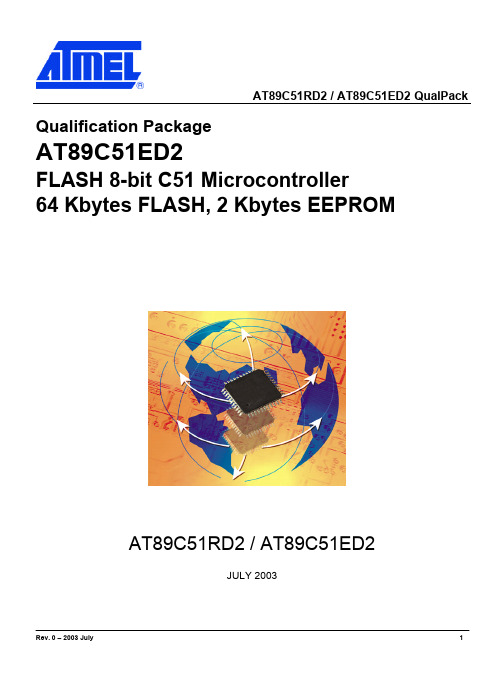
AT89C51RD2 / AT89C51ED2 QualPack Qualification PackageAT89C51ED2FLASH 8-bit C51 Microcontroller64 Kbytes FLASH, 2 Kbytes EEPROMAT89C51RD2 / AT89C51ED2JULY 2003AT89C51RD2 / AT89C51ED2 QualPack 1 Table of contents1TABLE OF CONTENTS (2)2GENERAL INFORMATION (3)3TECHNOLOGY INFORMATION (4)3.1W AFER P ROCESS T ECHNOLOGY (4)3.2P RODUCT D ESIGN (5)3.3D EVICE CROSS SECTION (6)4QUALIFICATION (7)4.1Q UALIFICATION M ETHODOLOGY (7)4.2Q UALIFICATION T EST M ETHODS (8)4.3W AFER L EVEL R ELIABILITY (9)4.3.1Electromigration (9)4.3.2Hot Carriers Injection (11)4.3.3Time Dependent Dielectric Breakdown (12)4.3.4FLASH Characteristics (14)4.4D EVICE R ELIABILITY (18)4.4.1Operating Life Testing (18)4.4.2ESD / Latch-up (18)4.4.3FLASH and EEPROM Data Retention and Endurance Cycling (18)4.4.4AT89C51ED2 Operating Reliability Calculation (20)4.5AT89C51ED2 P ACKAGING RELIABILITY (21)4.6AT89C51ED2 Q UALIFICATION STATUS (21)5ENVIRONMENTAL INFORMATION (22)6OTHER DATA (23)6.1ISO / TS16949 : 2002 C ERTIFICATE (23)6.2D ATA B OOK R EFERENCE (24)6.3R EVISION H ISTORY (24)AT89C51RD2 / AT89C51ED2 QualPack 2 General InformationProduct Name: AT89C51RD2Function: 8-bit Microcontroller with 64 Kbytes FLASHSPI InterfaceProduct Name: AT89C51E2Function: 8-bit Microcontroller with 64 Kbytes FLASH, 2 Kbytes EEPROMSPI InterfaceWafer Process: Logic CMOS 0.35 um with embedded FLASHAvailable Package Types PLCC 44, VQFP 44, PLCC 68, VQFP 68 ,PDIL 40Other Forms: Die, WaferLocations:Process Development, Atmel Colorado Springs, USAProduct Development Atmel Nantes, FranceWafer Plant Atmel Colorado Springs, USAQC Responsibility Atmel Nantes, FranceProbe Test Atmel Colorado Springs, USAAssembly Depending on packageFinal Test Atmel TSTI Manila, PhilippinesLot Release Atmel Nantes, FranceShipment Control Global Logistic Center, PhilippinesQuality Assurance Atmel Nantes, FranceReliability Testing Atmel Nantes, FranceFailure Analysis Atmel Nantes, FranceQuality ManagementAtmel Nantes, FranceSigned: Pascal LECUYERAT89C51RD2 / AT89C51ED2 QualPack 3 Technology Information3.1 Wafer Process TechnologyProcess Type (Name): Logic 0.35um with embedded FLASH (AT56800)Base Material: Epitaxied SiliconWafer Thickness (final) 475 umWafer Diameter 150 mmNumber Of Masks 27Gate Oxide (Logic transistors)Material Silicon DioxideThickness 68AGate Oxide (EPROM cell)Material Silicon DioxideThickness 390APolysiliconNumber of Layers 2Thickness Poly 1 1400A AmorphousThickness Poly 2 3200AMetalNumber of Layers 3Material: Aluminum CopperLayer 1 Thickness 5000ALayer 2 Thickness 5000ALayer 3 Thickness 8000APassivationMaterial Oxide HDP/ Oxy-nitrideThickness 21000AAT89C51RD2 / AT89C51ED2 QualPack 3.2 Product DesignDie Size 17,9 mm2Pad Size Opening / Pitch 66 um * 66 um / 111 umLogic Effective Channel Length 0.35 µmGate Poly Width (min.) 0.35 µmGate Poly Spacing (min.) 0.42 µmMetal 1 Width 0.42 µmMetal 1 Spacing 0.49 µmMetal 2 Width 0.56 µmMetal 2 Spacing 0.49 µmMetal 3 Width 0.56 µmMetal 3 Spacing 0.49 µmContact Size 0.35 µmContact Spacing 0.42 µmVia 1 Size 0.42 µmVia 2 Size 0.42 µmRev. 0 – 2003 July 5AT89C51RD2 / AT89C51ED2 QualPack 3.3 Device cross sectionAT56Kxx cross sectionAT89C51RD2 / AT89C51ED2 QualPack 4 Qualification4.1 Qualification MethodologyAll product qualifications are split into three distinct steps as shown below. Before a product is released for use, successful qualification testing are required at wafer, device and package level.- Wafer Level Reliability consists in testing individually basic process modules regarding their well known potential limitations (Electro-migration, Hot Carriers Injection, Oxide Breakdown, NVM Data Retention).Each test is performed using wafer process specific structures.- Device reliability is covering either dice design and processing aspects. The tests are performed on device under qualification, but generic data may also be considered for reliability calculation.- For each package type proposed in the Datasheet, it is verified that qualification data are available. If not qualification tests are carried out for the new package types. In addition, one package type is selected to verify packaging reliability of the device under qualification.AT89C51RD2 / AT89C51ED2 QualPack 4.2 Qualification Test MethodsGeneral Requirements for Plastic packaged CMOS ICs:Standard Test Description AcceptanceMIL-STD 883 Method 1005 Electrical Life Test (Early Failure Rate)48 hours 140°C0/300 - 48hMIL-STD 883 Method 1005 Electrical Life Test (Latent Failure Rate)1000 hours 140°C Dynamic or Static0/100 - 500hMIL-STD 883 Method 3015.7Electrostatic Discharge HBM+/-2000v 1.5kOhm/100pF/3 pulses0/3 per levelJEDEC 78 Latch up50mW power injection, 50% overvoltage @125°C0/5 per stressAEC Q100 Method 005NVM EnduranceProgram Erase Cycles 25°C0/50 - 10kcAEC Q100 Method 005NVM Data RetentionHigh Temperature Storage 165°C0/50 - 500hMIL-STD 883 Method 1010Temperature Cycling1000 cycles –65°C/150°C air/air0/50 - 500cAtmel PAQA0184 HAST after Preconditioning144 hours 130°C/85%RH0/50 – 96hEIA JESD22-A10185/85 Humidity Test1000 hours 85°C/85%RH0/50 - 500hEIA JESD22-A110HAST336 hours 130°C/85%RH0/50 - 168hEIA JEDEC 20-STDPreconditioningSoldering Stress 220°C/235°c/3 times0/11 per classMIL-STD 883Method 2003Solderability 0/3MIL-STD 883Method 2015Marking Permanency 0/5AT89C51RD2 / AT89C51ED2 QualPack 4.3 Wafer Level Reliability4.3.1 ElectromigrationPurpose:To evaluate the AT56800, AT35500, and AT37000 processes for Metal 1, Metal 3 &Via Electromigration Reliability. These 3 processes have the same steps for interconnect levels.Test Parameters:Metal 1 & Metal 3:Sample Size = 15Temp = 250C with Joule heating .J = 3.5E06 A/cm2.Via:Sample Size = 15Temp = 200C with Joule heating.J = 2.5E06 A/cm2.Black’s Equation Parameters:Failure Criteria - 10% increase in resistance. Data taken every 1% change.n = 2Ea = 0.6eVLifetime Predictions:Metal 1 :Split 1 - Tf.1% exp = ~ 28 hrs Tf.01% op = ~ 28 hrs x 39706 accel = 127 years.(Sigma = 2.7118 hours, Accel temp = 130, Accel current = 306)Metal 3 :Split 3 - Tf.1% exp = ~ 140 hrs Tf.01% op = ~ 140 hrs x 39706 accel = 634 years.(Sigma = 1.8782 hours, Accel temp = 130, Accel current = 306)VIA :Split 4 - Tf.1% exp = ~ 22 hrs Tf.1% op = ~ 22 hrs x 7144 accel = 18 years.(Sigma = 2.59 hours, Accel temp = 31.75, Accel current = 225) (9/15 fails)Conclusion:All splits pass the minimum 10 years lifetime.AT89C51RD2 / AT89C51ED2 QualPack Test results :AT56800 metal 1 results AT56800 metal 3 resultsAT56800 VIA resultsElectromigration summary table:Level SampleSizeFails @10%Tf.1%Lifetime (yrs)M1 15 9 140M3 15 7 1088Via 15 9 19AT89C51RD2 / AT89C51ED2 QualPack 4.3.2 Hot Carriers InjectionTest conditionsThe test is performed by forcing a high drain bias on the test device (Vds>Vddmax) to accelerate the carriers to the maximum. At the same time the gate bias (Vgs) is chosen in order to maximize the injection of carriers into the gate oxide and also the substrate. WLR_B n-channel W/L 0.35um/25um the stress is performed on a number of transistors, each at a different stress condition Vds,stress and Vgs,stress. For each transistor, the time to reach the failure criteria (dIdsat/Idsat=10%) is obtained. NMOS is more sensitive to hot carriers compared to PMOS. Consequently NMOS is the only structure tested.MeasurementAT568T7 lot 1J0433 has been measured using the WLR_B hot electron structure with standard drain.NMOS W/L = 25/0.35 um.ResultsConclusionThe extrapolated life time in the worst case conditions (@Vds=Vdd max & Vgs set to maximize substrate current) is much greater than 0.2 years in DC mode (qualification requirement) which is equivalent to more than 10 years in AC mode.AT89C51RD2 / AT89C51ED2 QualPack 4.3.3 Time Dependent Dielectric BreakdownPurpose:To evaluate the AT56800 thin gate oxide TDDB performance as follows:a) To determine the activation energy of gate oxide failures on STI active edge capacitorsb) To determine the field acceleration factor for intrinsic gate oxide failuresc) To determine the sigma the lognormal standard deviation of the time to breakdown distribution of theintrinsic gate oxideTest Parameters:Lot 9G3470 (wafers 4, 5, 18)Min thickness: 72.9AMax thickness: 74.7ACapacitor size: 6.267 um2The stress conditions used are shown below:Temperature/Field 9.5MV/cm 10.0MV/cm 10.5MV/cm225C N=5 N=5 N=5200C N=5 N=5 N=5175C N=5 N=5 N=6Accumulated total stress time: 132 hours / 46 capacitorsCalculation Parameters:Failure Criteria: 0.01% failuresTemp/Voltage use: 105°C / 3.3VOxide thickness: 63A (target –10%)Lifetime Prediction:The equation used to describe the breakdown of gate oxides is:Tbd(i) = exp(SIGMA*Z(i) + GAMMA*Eox +Ea/kT + T0)WhereTbd(i) is the time to breakdown of the i th capacitor,SIGMA is the lognormal standard deviation of the breakdown distribution,Z(i) is the Z-score of the i th capacitor (essentially the difference between its breakdown time and the mean measured in standard deviations),GAMMA is the Field acceleration constant,Eox is the oxide field,Ea is the activation energy of this failure mechanism,K is Boltzmann’s constant,T is the Kelvin Temperature, andT0 is a fitting constant.AT89C51RD2 / AT89C51ED2 QualPack The best fit coefficients in the regression analysis are:T0= 14.25034317 LN-secEa= 1.060043152 eVGAMMA= -3.2454227 LN-sec-cm/MVSIGMA= 0.414655753 LN-secwith an adjusted r-squared of 97.99%. The intrinsic lifetime at use conditions calculated from this regression is 56174 years.Conclusion:Using the coefficients determined above, the time to reach any cumulative percent failure level can be estimated given the stress conditions. Using 105C and 3.3 volts on 63 Angstrom N-Channel gate2 oxide, we may expect0.01% of capacitors having 6,267 square microns area with 6,174 microns of active edge to fail in about 613 years, exceeding the technology requirement of ten years.Test results :AT89C51RD2 / AT89C51ED2 QualPack 4.3.4 FLASH Characteristics4.3.4.1 Cell endurancePurpose:To evaluate the ability of memory cell to withstand high number of program/erase cycles without change of electrical characteristics.Test Parameters:Measurements have been done on lot 0R5414.Test done on 2 cells in a byte :- cell near byte select transistor, called bit0 (1st column)- cell near Vss contact, called bit 7 (8th column).Cycling is done for various programming voltages :- write : 13.5V on BL / 15.6V on select - clear : 13.5V on sense / 15.6V on select@5ms 14.5V on BL / 16.6V on select @5ms 14.5V on sense / 16.6V on select15.5V on BL / 17.6V on select 15.5V on sense / 17.6V on select16.5V on sense / 17.6V on selectAT89C51RD2 / AT89C51ED2 QualPack Conclusions:- Vt_wrt shift of 200 mV after 10k cycles- I_read decrease of 2.5 uA after 10kcycles (- 7 to 9 %)- No big difference between bit0 and bit 7 in terms of Vt or current variations Using the coefficients4.3.4.2 Cell retentionPurpose:To extrapolate cell life duration at 125°C from bake measurements at high temperature.Test parameters:Lot: 9T0930Temperature: 250°C and 200°CDuration: 92 hoursLifetime Prediction:The equation used to describe memory cell retention is:DVt (V) = A * (t[h])^m * exp (-1.05eV/kT[K])Results :Test measurements Extrapolated Life TimeConclusions :Extrapolation to 125°C - 10years = Vt loss is less than 0.8 mVAT89C51RD2 / AT89C51ED2 QualPack 4.3.4.3 Cell Read DisturbPurpose:To measure read disturb influence on 56k8 memory cell.Test parameters:Lot: 0t0348Programming: 14V on WL and sensegate @5msTemperature: 25°C and 140°CThe cell is stressed with BL voltage much higher than standard read conditions (around 6V) to accelerate disturb phenomenon : electrons from the Floating gate can move through the tunnel oxide. This charge loss is measured after stress by a Vt measurement.Test results:Conclusion:Extrapolation to 10 years lifetime give a maximum BL voltage of around 4V in read operation, which is much higher than nominal BL read voltage (~1V). So there is no sensitivity to read disturb either at room temperature or high temperature.AT89C51RD2 / AT89C51ED2 QualPack 4.3.4.4 Wafer probe Data retention measurementData retention has been verified after bake for 168 hours at 250°C on 3 wafers of a standard production lot. The results are summarized in the table below:Time to failureLot Wafer % Retention loss Failure rateextrapolation at 55°C1G4448 6 0% 3.91fit >> 10 years1G4448 8 0% 4.19fit >> 10 years1G4448 12 0% 3..96fit >> 10 yearsTotal 0% 1.34fit >> 10 years Conclusion:Data Retention measurements at wafer probe stand out high data retention capability of AT56800 products, exceeding the technology requirement of ten years.AT89C51RD2 / AT89C51ED2 QualPack 4.4 Device Reliability4.4.1 Operating Life TestingAT89C51ED2 test results are summarized in the table below.Lot Device Type Test Description Step Result CommentA01948K AT89C51ED2PLCC 44 EFR Dynamic Life Test 12h48h0/3000/300LFR Dynamic Life Test 500h1000h0/1000/1004.4.2 ESD / Latch-upAT89C51ED2 test results are summarized in the table below.Lot Device Type Test Description Step Result CommentA01948 AT89C51ED2PLCC 44 ESD-HBM Model 2000V3000V4000V5000V0/31/31/31/3Class 2 of MIL STD 883LATCH-UPOver-VoltagePower Injection5.5v50mW0/50/5Test done at 125°CClassified latch-up free4.4.3 FLASH and EEPROM Data Retention and Endurance CyclingAT89C51ED2 test results are summarized in the table below.Lot Device Type Test Description Step Result CommentA01948K AT89C51ED2PLCC 44 Data Retention 500h1000h0/500/50Program / EraseEndurance Cycling100kc 0/30 32k USER memoryProgram / EraseEndurance Cycling100kc 0/30 2k DATA memoryAT89C51RD2 / AT89C51ED2 QualPack AT56800 Program / Erase Endurance:Temperature acceleration factor calculation:AT56800 FLASH / EEPROM Reliability Calculation:Global Calculation AT56800MicrocontrollersData-Retention Test 165°c250°c0/11010000/251496For current sample sizeexpressed in device*hours,Ea = 0.7eV, CL = 60%, T = 55°:?DR= 0.29 fitEndurance Cycling 55°c 1/109850k Failure : 1 bit charge lossFor sample size expressed inequivalent cycles at 55°c, andassuming one cycle per day,Ea = 0.25eV, CL = 60%:?EC= 0.76 fitAT89C51RD2 / AT89C51ED2 QualPack4.4.4 AT89C51ED2 Operating Reliability CalculationIn the next table, it is proposed a AT89C51ED2 reliability prediction calculated at 55°c for 60% confidence level from generic test data collected over the 12 last months process monitor.Lots Device Type Test Description Step Result CommentA00648 P01709 A00988B T89C51CC01VQFP 44EFR Dynamic Life Test 48h 0/3787A01459AA01460EA01615BLFR Dynamic Life Test 1000h 0/266A01110C A01110D T89C51CC02SOIC28EFR Dynamic Life Test 48h 1/1260 1 Ipd drift caused by scratch onmetal 1A01185FA01366ELFR Dynamic Life Test 1000h 0/280A01679A A01679B T89C51RC2PLCC 44EFR Dynamic Life Test 48h 0/1856LFR Dynamic Life Test 1000h 0/100A00808A A00943E T89C51RB2PLCC 44EFR Dynamic Life Test 48h 0/300LFR Dynamic Life Test 1000h 0/100A01487Q A02179 T85C5121T89C5121EFR Dynamic Life Test 48h 0/684 SSOP24 LFR Dynamic Life Test 1000h 0/100A01435H A01435K AT89C5114SOIC20EFR Dynamic Life Test 48h 0/1887A02293C LFR Dynamic Life Test 1000h 0/200A00960C A01808A AT89C51SND1AT83C51SND1EFR Dynamic Life Test 48h 1/550 Consumption hot spot in DCLKinput bufferA01914J VQFP 80 LFR Dynamic Life Test 1000h 0/170A01584A AT89C5131VQFP64EFR Dynamic Life Test 48h 0/350LFR Dynamic Life Test 1000h 0/100Global EFR Dynamic Life Test 48h 2/10674 187 ppmLFR Dynamic Life Test - 0/1316 4.4 fitAT89C51RD2 / AT89C51ED2 QualPack4.5 AT89C51ED2 Packaging reliabilityIn this section are presented the packaging qualification measurements carried out in PLCC 44.Lots Device Type Test Description Step Result CommentA01948K AT89C51ED2PLCC 44 Humidity 85/85 postPreconditioning level 1500h 0/500/50Thermal Cycles postPreconditioning L1500c1000c0/500/50Autoclave post thermalshocks and Precond. L196h 0/50A01679C AT89C51RC2PLCC44 Preconditioning level 1 SAMVisualElect.0/110/500/50 Thermal Cycles postPreconditioning L1500c1000c0/500/50Humidity 85/85 postPreconditioning level 1500h 0/500/50Autoclave post thermalshocks and Precond. L196h 0/50High TemperatureStorage500h1000h0/500/50 Marking permanency Visual 0/54.6 AT89C51ED2 Qualification statusAtmel digital 0.35 um wafer process is qualified since 1999, October.Derived from this technology, AT89C51RD2 / AT89C51ED2 have passed successfully Reliability Testing. Full qualification has been pronounced in June 2003.All package pass Level 1 of Moisture Sensitivity Ranking as per JESD 20B. Therefore, Dry Packing is not mandatory.AT89C51RD2 / AT89C51ED2 QualPack5 Environmental InformationAtmel Nantes Environmental Policy aims are :- Reducing the use of harmful chemicals in its processes- Reducing the content of harmful materials in its products- Using re-usable materials wherever possible- Reducing the energy content of its productsAs part of that plan, Ozone Depleting Chemicals are being replaced either by Atmel Nantes or its sub-contractors. Atmel Nantes site is ISO14001 certified since May 2000.AT89C51RD2 / AT89C51ED2 QualPack 6 Other Data6.1 ISO / TS16949 : 2002 CertificateAT89C51RD2 / AT89C51ED2 QualPack6.2 Data Book ReferenceThe data sheet is available upon request to sales representative or upon direct access on Atmel web site:/Address ReferencesAll inquiries relating to this document should be addressed to the following:Atmel NantesBP7060244306 Nantes Cedex 3FranceTelephone (33) 2 40 18 18 18Telefax (33) 2 40 18 19 00Or direct contactPascal LECUYERTelephone (33) 2 40 18 17 73Telefax (33) 2 40 18 19 466.3 Revision HistoryIssue Modification Notice Application Date0 Initial Product Evaluation 2003 JulyRemarks:The information given in this document is believed to be accurate and reliable. However, no responsibility is assumed by Atmel for its use. No specific guarantee or warranty is implied or given by this data unless agreed in writing elsewhere.Atmel reserves the right to update or modify this information without notification, at any time, in the interest of providing the latest information.Parts of this publication may be reproduced without special permission on the condition that our author and source are quoted and that two copies of such extracts are placed at our disposal after publication. Before use of such reproduced material the user should check that the information is current.Written permission must be obtained from the publisher for complete reprints or translations。
AT89C51单片机中文资料

AT89C51单片机中文资料AT89C51是一种带4K字节闪烁可编程可擦除只读存储器(FPEROM—Falsh Programmable and Erasable Read Only Memory)的低电压,高性能CMOS8位微处理器,俗称单片机.2.管脚说明:VCC:供电电压。
GND:接地。
P0口:P0口为一个8位漏级开路双向I/O口,每脚可吸收8TTL门电流。
当P1口的管脚第一次写1时,被定义为高阻输入。
P0能够用于外部程序数据存储器,它可以被定义为数据/地址的第八位。
在FIASH编程时,P0 口作为原码输入口,当FIASH进行校验时,P0输出原码,此时P0外部必须被拉高。
P1口:P1口是一个内部提供上拉电阻的8位双向I/O口,P1口缓冲器能接收输出4TTL门电流。
P1口管脚写入1后,被内部上拉为高,可用作输入,P1口被外部下拉为低电平时,将输出电流,这是由于内部上拉的缘故。
在FLASH编程和校验时,P1口作为第八位地址接收.P2口:P2口为一个内部上拉电阻的8位双向I/O口,P2口缓冲器可接收,输出4个TTL门电流,当P2口被写“1"时,其管脚被内部上拉电阻拉高,且作为输入。
并因此作为输入时,P2口的管脚被外部拉低,将输出电流。
这是由于内部上拉的缘故.P2口当用于外部程序存储器或16位地址外部数据存储器进行存取时,P2口输出地址的高八位.在给出地址“1”时,它利用内部上拉优势,当对外部八位地址数据存储器进行读写时,P2口输出其特殊功能寄存器的内容。
P2口在FLASH编程和校验时接收高八位地址信号和控制信号。
P3口:P3口管脚是8个带内部上拉电阻的双向I/O口,可接收输出4个TTL门电流.当P3口写入“1”后,它们被内部上拉为高电平,并用作输入。
作为输入,由于外部下拉为低电平,P3口将输出电流(ILL)这是由于上拉的缘故。
P3口也可作为AT89C51的一些特殊功能口,如下表所示:口管脚备选功能P3.0 RXD(串行输入口)P3。
RC4190资料

125 70 150
375 4.17 6.25 8.33
mA mW/°C mW/°C mW/°C
Operating Conditions
Parameter θJC θJA Thermal resistance Thermal resistance CerDIP SOIC PDIP CerDIP Min Typ 45 200 160 120 Max Units °C/W °C/W °C/W °C/W
3
PRODUCT SPECIFICATION
பைடு நூலகம்
RC4190
Electrical Characteristics
(+VS = +6.0V, IC = 5.0 µA, and TA = +25°C unless otherwise noted.) RM4190 Symbol +VS VREF ISW ISY ef Parameters Supply Voltage Reference Voltage (Internal) Switch Current Supply Current Efficiency Line Regulation LI FO IC ICO Load Regulation Operating Frequency Range Reference Set Current Switch Leakage Current Supply Current (Disabled) Low Battery Bias Current Capacitor Charging Current Oscillator Frequency Tolerance +VTHX -VTHX IFB ILBD Capacitor Threshold Voltage + Capacitor Threshold Voltage – Feedback Input Current Low Battery Output Current V7 = 1.3V V8 = 0.4V, V1 = 1.1V 500 V4 = 24V (RC4190) 30V (RM4190, RC4190A) VC ≤ 200 mV V1 = 1.2V 0.5 VOUT < VS < VOUT VS = +0.5 VOUT PL = 150 mW 0.1 1.0 V4 = 400 mV Measure at Pin 5 I4 = 0 Conditions Min 2.2 1.29 100 1.31 200 215 85 0.04 0.2 25 5.0 0.01 0.2 0.5 75 50 5.0 0.1 1.0 300 Typ Max 30 1.33 Min 2.2 1.24 100 1.31 200 215 85 0.04 0.2 25 5.0 0.01 0.5 0.5 75 50 5.0 300 RC4190 Typ Max 24 1.38 Units V V mA µA % % VO % VO kHz µA µA
P89V51中文手册
P89V51RB2/RC2/RD2 器件手册
专注的力量成就梦想
资料翻译
资料翻译
目录
目录
第 1 章 概述 ....................................................................................................................................1 第 2 章 特性 ....................................................................................................................................2 第 3 章 订购信息 ............................................................................................................................3
5.1 管脚....................................................................................................................................5 5.2 管脚描述............................................................................................................................7 第 6 章 特殊功能寄存器...............................................................................................................10 第 7 章 功能描述 ..........................................................................................................................13 7.1 存储器结构......................................................................................................................13
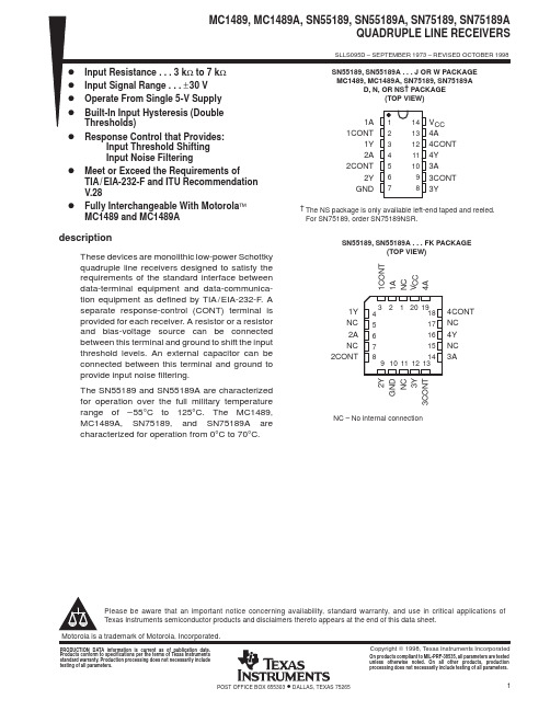
SN55189FK中文资料
元器件交易网IMPORTANT NOTICETexas Instruments and its subsidiaries (TI) reserve the right to make changes to their products or to discontinueany product or service without notice, and advise customers to obtain the latest version of relevant informationto verify, before placing orders, that information being relied on is current and complete. All products are soldsubject to the terms and conditions of sale supplied at the time of order acknowledgement, including thosepertaining to warranty, patent infringement, and limitation of liability.TI warrants performance of its semiconductor products to the specifications applicable at the time of sale inaccordance with TI’s standard warranty. Testing and other quality control techniques are utilized to the extentTI deems necessary to support this warranty. Specific testing of all parameters of each device is not necessarilyperformed, except those mandated by government requirements.CERTAIN APPLICATIONS USING SEMICONDUCTOR PRODUCTS MAY INVOLVE POTENTIAL RISKS OFDEATH, PERSONAL INJURY, OR SEVERE PROPERTY OR ENVIRONMENTAL DAMAGE (“CRITICALAPPLICATIONS”). TI SEMICONDUCTOR PRODUCTS ARE NOT DESIGNED, AUTHORIZED, ORWARRANTED TO BE SUITABLE FOR USE IN LIFE-SUPPORT DEVICES OR SYSTEMS OR OTHERCRITICAL APPLICATIONS. INCLUSION OF TI PRODUCTS IN SUCH APPLICATIONS IS UNDERSTOOD TOBE FULLY AT THE CUSTOMER’S RISK.In order to minimize risks associated with the customer’s applications, adequate design and operatingsafeguards must be provided by the customer to minimize inherent or procedural hazards.TI assumes no liability for applications assistance or customer product design. TI does not warrant or representthat any license, either express or implied, is granted under any patent right, copyright, mask work right, or otherintellectual property right of TI covering or relating to any combination, machine, or process in which suchsemiconductor products or services might be or are used. TI’s publication of information regarding any thirdparty’s products or services does not constitute TI’s approval, warranty or endorsement thereof.Copyright © 1998, Texas Instruments Incorporated。
RE46C190光电式烟雾探测器
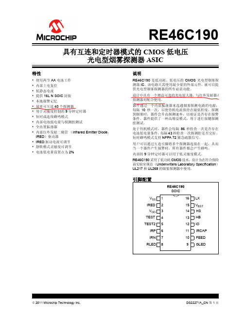
LX 16 VBST 15
HS 14 HB 13 IO 12 IRCAP11 FEED10 GLED 9
L1 10 µH
D1
R4 C5 1.5M 1 nF
R5 C6 330 33 µF
VBST
R3 200K
C4 4.7 µF
至其他器件
注 1: C2 应尽可能靠近器件电源引脚放置, C1 应尽可能靠近 VSS 引脚放置。 2: R3、 R4 和 C5 均为典型值,可通过调节它们来最大程度提高声压。
VBST = 5V, IRCAP = 5V,
(选择 150 mA 选项;
TA = 27°C)
IIRED200
2
180
200
220
mA IRED 点亮, VIRED = 1V,
VBST = 5V, IRCAP = 5V,
(选择 200 mA 选项;
TA = 27°C)
IRED 电流温度系数 TCIRED
VBST = 5V, IRCAP = 5V,
(选择 50 mA 选项;
TA = 27°C)
IIRED100
2
90
100
110
mA IRED 点亮, VIRED = 1V,
VBST = 5V, IRCAP = 5V,
(选择 100 mA 选项;
TA = 27°C)
IIRED150
2
135
150
165
mA IRED 点亮, VIRED = 1V,
µA VIN = VDD
输出低电压 输出高电压
IPDIO2
12
—
—
140
µA VIN = 15V
VOL1
13, 14
74和cd系列详细资料

常用74系列标准数字电路的中文名称资料器件代号器件名称74 74LS 74HC00 四2输入端与非门√ √ √01 四2输入端与非门(OC) √ √02 四2输入端或非门√ √ √03 四2输入端与非门(OC) √ √04 六反相器√ √ √05 六反相器(OC) √ √06 六高压输出反相器(OC,30V) √ √07 六高压输出缓冲,驱动器(OC,30V) √ √ √08 四2输入端与门√ √ √09 四2输入端与门(OC) √ √ √10 三3输入端与非门√ √ √11 三3输入端与门√ √12 三3输入端与非门(OC) √ √ √13 双4输入端与非门√ √ √14 六反相器√ √ √15 三3输入端与门(OC) √ √16 六高压输出反相器(OC,15V) √17 六高压输出缓冲,驱动器(OC,15V) √20 双4输入端与非门√ √ √21 双4输入端与门√ √ √22 双4输入端与非门(OC) √ √25 双4输入端或非门(有选通端) √ √ √26 四2输入端高压输出与非缓冲器√ √ √27 三3输入端或非门√ √ √28 四2输入端或非缓冲器√ √ √30 8输入端与非门√ √ √32 四2输入端或门√ √ √33 四2输入端或非缓冲器(OC) √ √37 四2输入端与非缓冲器√ √38 四2输入端与非缓冲器(OC) √ √40 双4输入端与非缓冲器√ √ √42 4线-10线译码器(BCD输入) √ √43 4线-10线译码器(余3码输入) √44 4线-10线译码器(余3葛莱码输入) √48 4线-7段译码器√49 4线-7段译码器√50 双2路2-2输入与或非门√ √ √51 2路3-3输入,2路2-2输入与或非门√ √ √52 4路2-3-2-2输入与或门√53 4路2-2-2-2输入与或非门√54 4路2-3-3-2输入与或非门√ √55 2路4-4输入与或非门√60 双4输入与扩展器√ √61 三3输入与扩展器√62 4路2-3-3-2输入与或扩展器√64 4路4-2-3-2输入与或非门√65 4路4-2-3-2输入与或非门(OC) √70 与门输入J-K触发器√71 与或门输入J-K触发器√72 与门输入J-K触发器√74 双上升沿D型触发器√ √78 双D型触发器√ √85 四位数值比较器√86 四2输入端异或门√ √ √87 4位二进制原码/反码√95 4位移位寄存器√101 与或门输入J-K触发器√102 与门输入J-K触发器√107 双主-从J-K触发器√108 双主-从J-K触发器√109 双主-从J-K触发器√110 与门输入J-K触发器√111 双主-从J-K触发器√ √112 双下降沿J-K触发器√113 双下降沿J-K触发器√114 双下降沿J-K触发器√116 双4位锁存器√120 双脉冲同步驱动器√121 单稳态触发器√ √ √122 可重触发单稳态触发器√ √ √123 可重触发双稳态触发器√ √ √125 四总线缓冲器√ √ √126 四总线缓冲器√ √ √128 四2输入端或非线驱动器√ √ √132 四2输入端与非门√ √ √常用4000系列标准数字电路的中文名称资料型号器件名称厂牌备注CD4000 双3输入端或非门+单非门TICD4001 四2输入端或非门HIT/NSC/TI/GOLCD4002 双4输入端或非门NSCCD4006 18位串入/串出移位寄存器NSCCD4007 双互补对加反相器NSCCD4008 4位超前进位全加器NSCCD4009 六反相缓冲/变换器NSCCD4010 六同相缓冲/变换器NSCCD4011 四2输入端与非门HIT/TICD4012 双4输入端与非门NSCCD4013 双主-从D型触发器FSC/NSC/TOSCD4014 8位串入/并入-串出移位寄存器NSCCD4015 双4位串入/并出移位寄存器TICD4016 四传输门FSC/TICD4017 十进制计数/分配器FSC/TI/MOTCD4018 可预制1/N计数器NSC/MOTCD4019 四与或选择器PHICD4020 14级串行二进制计数/分频器FSCCD4021 08位串入/并入-串出移位寄存器PHI/NSCCD4022 八进制计数/分配器NSC/MOTCD4023 三3输入端与非门NSC/MOT/TICD4024 7级二进制串行计数/分频器NSC/MOT/TICD4025 三3输入端或非门NSC/MOT/TICD4026 十进制计数/7段译码器NSC/MOT/TICD4027 双J-K触发器NSC/MOT/TICD4028 BCD码十进制译码器NSC/MOT/TICD4029 可预置可逆计数器NSC/MOT/TICD4030 四异或门NSC/MOT/TI/GOLCD4031 64位串入/串出移位存储器NSC/MOT/TICD4032 三串行加法器NSC/TICD4033 十进制计数/7段译码器NSC/TICD4034 8位通用总线寄存器NSC/MOT/TICD4035 4位并入/串入-并出/串出移位寄存NSC/MOT/TI CD4038 三串行加法器NSC/TICD4040 12级二进制串行计数/分频器NSC/MOT/TICD4041 四同相/反相缓冲器NSC/MOT/TICD4042 四锁存D型触发器NSC/MOT/TICD4043 4三态R-S锁存触发器("1"触发) NSC/MOT/TI CD4044 四三态R-S锁存触发器("0"触发) NSC/MOT/TI CD4046 锁相环NSC/MOT/TI/PHICD4047 无稳态/单稳态多谐振荡器NSC/MOT/TICD4048 4输入端可扩展多功能门NSC/HIT/TICD4049 六反相缓冲/变换器NSC/HIT/TICD4050 六同相缓冲/变换器NSC/MOT/TICD4051 八选一模拟开关NSC/MOT/TICD4052 双4选1模拟开关NSC/MOT/TICD4053 三组二路模拟开关NSC/MOT/TICD4054 液晶显示驱动器NSC/HIT/TICD4055 BCD-7段译码/液晶驱动器NSC/HIT/TI CD4056 液晶显示驱动器NSC/HIT/TICD4059 “N”分频计数器NSC/TICD4060 14级二进制串行计数/分频器NSC/TI/MOT CD4063 四位数字比较器NSC/HIT/TICD4066 四传输门NSC/TI/MOTCD4067 16选1模拟开关NSC/TICD4068 八输入端与非门/与门NSC/HIT/TICD4069 六反相器NSC/HIT/TICD4070 四异或门NSC/HIT/TICD4071 四2输入端或门NSC/TICD4072 双4输入端或门NSC/TICD4073 三3输入端与门NSC/TICD4075 三3输入端或门NSC/TICD4076 四D寄存器CD4077 四2输入端异或非门HITCD4078 8输入端或非门/或门CD4081 四2输入端与门NSC/HIT/TICD4082 双4输入端与门NSC/HIT/TICD4085 双2路2输入端与或非门CD4086 四2输入端可扩展与或非门CD4089 二进制比例乘法器CD4093 四2输入端施密特触发器NSC/MOT/ST CD4094 8位移位存储总线寄存器NSC/TI/PHICD4095 3输入端J-K触发器CD4096 3输入端J-K触发器CD4097 双路八选一模拟开关CD4098 双单稳态触发器NSC/MOT/TICD4099 8位可寻址锁存器NSC/MOT/STCD40100 32位左/右移位寄存器CD40101 9位奇偶较验器CD40102 8位可预置同步BCD减法计数器CD40103 8位可预置同步二进制减法计数器CD40104 4位双向移位寄存器CD40105 先入先出FI-FD寄存器CD40106 六施密特触发器NSC\TICD40107 双2输入端与非缓冲/驱动器HAR\TICD40108 4字×4位多通道寄存器CD40109 四低-高电平位移器CD40110 十进制加/减,计数,锁存,译码驱动STCD40147 10-4线编码器NSC\MOTCD40160 可预置BCD加计数器NSC\MOTCD40161 可预置4位二进制加计数器NSC\MOTCD40162 BCD加法计数器NSC\MOTCD40163 4位二进制同步计数器NSC\MOTCD40174 六锁存D型触发器NSC\TI\MOTCD40175 四D型触发器NSC\TI\MOTCD40181 4位算术逻辑单元/函数发生器CD40182 超前位发生器CD40192 可预置BCD加/减计数器(双时钟) NSC\TI CD40193 可预置4位二进制加/减计数器NSC\TICD40194 4位并入/串入-并出/串出移位寄存NSC\MOT CD40195 4位并入/串入-并出/串出移位寄存NSC\MOT CD40208 4×4多端口寄存器CD4501 4输入端双与门及2输入端或非门CD4502 可选通三态输出六反相/缓冲器CD4503 六同相三态缓冲器CD4504 六电压转换器CD4506 双二组2输入可扩展或非门CD4508 双4位锁存D型触发器CD4510 可预置BCD码加/减计数器CD4511 BCD锁存,7段译码,驱动器CD4512 八路数据选择器CD4513 BCD锁存,7段译码,驱动器(消隐)CD4514 4位锁存,4线-16线译码器CD4515 4位锁存,4线-16线译码器CD4516 可预置4位二进制加/减计数器CD4517 双64位静态移位寄存器CD4518 双BCD同步加计数器CD4519 四位与或选择器CD4520 双4位二进制同步加计数器CD4521 24级分频器CD4522 可预置BCD同步1/N计数器CD4526 可预置4位二进制同步1/N计数器CD4527 BCD比例乘法器CD4528 双单稳态触发器CD4529 双四路/单八路模拟开关CD4530 双5输入端优势逻辑门CD4531 12位奇偶校验器CD4532 8位优先编码器CD4536 可编程定时器CD4538 精密双单稳CD4539 双四路数据选择器CD4541 可编程序振荡/计时器CD4543 BCD七段锁存译码,驱动器CD4544 BCD七段锁存译码,驱动器CD4547 BCD七段译码/大电流驱动器CD4549 函数近似寄存器CD4551 四2通道模拟开关CD4553 三位BCD计数器CD4555 双二进制四选一译码器/分离器CD4556 双二进制四选一译码器/分离器CD4558 BCD八段译码器CD4560 "N"BCD加法器CD4561 "9"求补器CD4573 四可编程运算放大器CD4574 四可编程电压比较器CD4575 双可编程运放/比较器CD4583 双施密特触发器CD4584 六施密特触发器CD4585 4位数值比较器CD4599 8位可寻址锁存器CD22100 4×4×1交叉点开关。
at89c51中文资料_数据手册_参数

万联芯城 电子元器件物料全国供应,专业提 供电子元器件原装现货产品,1 片起订,价格优势明显,电子元 器件采购网万联芯城目前为长电科技,顺络电子,先科 ST 等多 家知名原厂的指定授权代理商,专为客户提供电子元器件配单业 务,提交物料清单即可当天报价当天发货,点击进入万联芯城。
AT89C51是一种低功耗、高性能的CMOS 8位微型计算机,具有4Kbytes的Flash可编程只读 存储器(PEROM)。该设备使用Atmel的高密度非易失性存储器技术制造,与工业标准的 MCS-51指令集和pinout兼容。芯片上的闪存可以让程序内存在系统内重新编程,也可以 由一个召集人的非易失性内存程序员来重新编程。Atmel AT89C51是一种功能强大的微型 计算机,它将一个多用途的8位CPU与闪存芯片结合在一起,为许多嵌入式控制应用程序 提供了一种高灵活性和高性价比的解决方案。AT89C51提供了以下标准特性:4Kbytes的 Flash, 128字节的RAM, 32个I/O行,两AT89C51个16位的计时器/计数器,一个五个矢量的 二级中断架构,一个完整的双工串口,片上振荡器和时钟圈-cuitry。此外,AT89C51采用 静态逻辑设计,可将操பைடு நூலகம்频率降至零,支持两种软件可选择的节能模式。空闲的适当操 作CPU,同时允许RAM、计时器/计数器、串行端口和中断系统继续运行。电源关闭模式 保存RAM内容,但冻结振荡器禁用所有其他芯片功能,直到下一个硬件复位。销 DescriptionVCCSupply voltage.GNDGround。端口0Port 0是一个8位开路双向I/O端口。作为 输出端口,每个引脚可以接收8个TTLAT89C51输入。当1被写入端口0时,这些引脚可以 作为高阻抗输入。端口0也可以配置为在访问外部pro-gram和数据内存期间的多路低阶地 址/数据总线。在这种模式下,P0具有内浆。端口0也在Flash编程期间接收代码字节,并 输出代码字节du环编程验证。AT89C51在程序验证过程中需要外部的pullups。端口1是一 个8位双向I/O端口,具有内部pullups。端口1输出缓冲区可以接收/源4个TTL输入。当1s被 写入端口1引脚时,它们被内部的脉冲拉高,并可作为输入。作为输入,外部被拉低的端 口1引脚会因为内部的pullups而变酸(IIL)。端口1也在flash编程和验证过程中接收低阶地址 字节。端口2Port 2是一个带有内部pullups的8位双向I/O端口。端口2输出缓冲区可以接收/ 源4个TTL输入。当1s被写到端口2时,它们被内部的pullups拉得很高,可以用作输入。作 为输入,外部被拉低的端口2引脚会因为内部的脉冲而变酸。端口2在从外部程序内存获 取和访问使用16位地址的外部数据内存(MOVX @DPTR)期间发出高阶地址字节。在这个 应用中,当发射1s时,它使用强的内部拉升。在访问使用8位地址(MOVX @ RI)的外部数 据存储器时,端口2发出P2专AT89C51用函数寄存器的核心。端口2还在Flash编程和验证 过程中接收高阶地址位和somecontrol信号。端口3Port 3是一个8位双向I/O端口,具有内部 pullups。端口3输出缓冲区可以接收/源四个TTL输入。当1s被写到端口3时,它们被内部的 pullups拉得很高,可以用作输入。作为输入,外部被拉低的端口3引脚会因为pullups而变 酸(IIL)。端口3还具有AT89C51的各种特殊功能,如下所示在每次访问外部数据时都跳过 了pulse。如果需要,可以通过设置sfr位置8EH的0位来禁用ALE操作。在位集上,ALE只 在一个MOVX或MOVC指令中活动。否则,大头针就会弱拉高。如果微控制器处于外部 执行模式,则设置禁用“禁用”的位就没有效果。PSENProgram Store启用的是read strobe 到外部的pro-AT89C51gram内存。当AT89C51执行来自外部pro-gram内存的代码时,每个 machinecycle都会激活PSEN两次,除了在每次访问外部数据内存时跳过两次PSEN激 活。EA / VPPExternal访问启用AT89C51。必须将EA绑定到GND,以使设备能够从从从 0000H到FFFFH的外部pro-gram内存位置获取代码。然而,请注意,如果锁位1被编 程,EA将在复位时被内部锁住。EA应该绑定到VCC以执行内部程序。在Flash编程中,这 个pin还能接收12伏的编程实现volt-age (VPP),这是需要12伏VPP的部件。XTAL1Input输入到逆变振荡器放大器,输入到内部时 钟运行电路。XTAL2Output逆变振荡器放大器的输出。振荡器特性sxtal1和XTAL2分别是 逆变放大器的输入和输出,可以配置为使用asan片上振荡器,如图1所示。可以使用石英 晶体或陶瓷谐振器。要从外部时钟源驱动设备,XTAL2应该保持左连接,而XTAL1应该 被驱动,如图2所示。在外部时钟信号的工作周期中没有要求,因为内部时钟电路的输入 是通过两个触发器,但是最小和最大的电压高AT89C51和低的时间规格必须被观察。在 空闲模式下,CPU自动进入休眠状态,而所有的片上外围设备仍然处于活动状态。模式 是由软件调用的。在此模式下,片上RAM的内容和所有的spe函数寄存器都保持不变。空 闲模式可以通过任何启用的中断或硬件重置来终止。应该注意的是,当空闲被硬件 AT89C51重置终止时,设备通常会恢复程序执行,从它停止的地方开始,直到内部复位 算法控制之前的两个机器周期。在这种情况下,芯片上的硬件存储限制了对内部RAM的 访问,AT89C51但是对端口引脚的访问是不受限制的。为了消除AT89C51在空闲时对端口 pin进行意外写入的可能性,可以通过重置来终止,调用idleshnd的指令后面的指令不应该 是写入端口pin或外部内存的指令
新编俄罗斯电子器件对照手册资料

俄型号:К133ИЕ2十进制计数器说明相应国内外产品К133ИЕ2型单片TTL中规模半□中国型号导体集成电路,由四个主从触发器和附加推荐替换 SG5490A门电路组成,功能为具有清零和置9输入生产厂家 4435厂端的负沿触发异步十进制计数器。
其计数□国外型号 SN5490A (美国)长度可以是2、5、10分频。
К133ИЕ2主要参数 5490A主要参数 (T A=25℃)К133ИЕ2逻辑图和外引线排列 5490A功能表和外引线排列俄型号:К133ИЕ54位二进制计数器说明相应国内外产品К133ИЕ5型单片TTL中规模半□中国型号导体集成电路,由四个主从触发器和附加推荐替换 SG5493A门电路组成。
可组成二分频计数器和三级生产厂家 4435厂二进制计数器,具有清零输入端。
□国外型号 SN5493A (美国)AК133ИЕ5逻辑图和外引线排列 5493A功能表和外引线排列俄型号:К133ЛА28输入与非门说明相应国内外产品К133ЛА2型单片TTL小规模半□中国型号导体集成电路,功能为8输入端与非门。
推荐替换 JT5430生产厂家 4435厂□国外型号 SN5430 (美国)К133ЛА2逻辑图和外引线排列 5430逻辑图和外引线排列俄型号:К133ЛА3四2输入与非门说明相应国内外产品К133ЛА3型单片TTL小规模半□中国型号导体集成电路,由四个独立的而又完全相推荐替换 JT5400同的2输入端与非门组成。
生产厂家 4435厂□国外型号 SN5400 (美国)AК133ЛА3逻辑图和外引线排列 5400逻辑图和外引线排列说明相应国内外产品К133ЛА4型单片TTL小规模半□中国型号导体集成电路,由三个独立的而又完全相推荐替代 JT5410同的3输入端与非门组成。
生产厂家 4435厂□国外型号 SN5410 (美国)AК133ЛА4逻辑图和外引线排列* 5410逻辑图和外引线排列*注:俄产品输出脚顺序与5410不同,选用时应注意。
常用4000系列标准数字电路的中文名称

常用4000系列标准数字电路的中文名称资料74系列芯片功能大全〔点击型号查货〕常用74系列标准数字电路的中文名称资料器件代号器件名称74 74LS 74HCCD4000 双3输入端或非门+单非门TI 7400 TTL 2输入端四与非门00 四2输入端与非门√√√CD4001 四2输入端或非门HIT/NSC/TI/GOL 7401 TTL 集电极开路2输入端四与非门01 四2输入端与非门(OC) √√CD4002 双4输入端或非门NSC 7402 TTL 2输入端四或非门02 四2输入端或非门√√√CD4006 18位串入/串出移位存放器NSC 7403 TTL 集电极开路2输入端四与非门03 四2输入端与非门(OC) √√CD4007 双互补对加反相器NSC 7404 TTL 六反相器04 六反相器√√√CD4008 4位超前进位全加器NSC 7405 TTL 集电极开路六反相器05 六反相器(OC) √√CD4009 六反相缓冲/变换器NSC 7406 TTL 集电极开路六反相高压驱动器06 六高压输出反相器(OC,30V) √√CD4010 六同相缓冲/变换器NSC 7407 TTL 集电极开路六正相高压驱动器07 六高压输出缓冲,驱动器(OC,30V) √√√CD4011 四2输入端与非门HIT/TI 7408 TTL 2输入端四与门08 四2输入端与门√√√CD4012 双4输入端与非门NSC 7409 TTL 集电极开路2输入端四与门09 四2输入端与门(OC) √√√CD4013 双主-从D型触发器FSC/NSC/TOS 7410 TTL 3输入端3与非门10 三3输入端与非门√√√CD4014 8位串入/并入-串出移位存放器NSC7411 TTL 3输入端3与门11 三3输入端与门√√CD4015 双4位串入/并出移位存放器TI 7412 TTL 开路输出3输入端三与非门12 三3输入端与非门(OC) √√√CD4016 四传输门FSC/TI 7413 TTL 4输入端双与非施密特触发器13 双4输入端与非门√√√CD4017 十进制计数/分配器FSC/TI/MOT 7414 TTL 六反相施密特触发器14 六反相器√√√CD4018 可预制1/N计数器NSC/MOT 7415 TTL 开路输出3输入端三与门15 三3输入端与门(OC) √√CD4019 四与或选择器PHI 7416 TTL 开路输出六反相缓冲/驱动器16 六高压输出反相器(OC,15V) √CD4020 14级串行二进制计数/分频器FSC 7417 TTL 开路输出六同相缓冲/驱动器17 六高压输出缓冲,驱动器(OC,15V) √CD4021 08位串入/并入-串出移位7420 TTL 4输入端双与非20 双4输入端与非门√√√存放器PHI/NSC 门CD4022 八进制计数/分配器NSC/MOT7421 TTL 4输入端双与门21 双4输入端与门√√√CD4023 三3输入端与非门NSC/MOT/TI 7422 TTL 开路输出4输入端双与非门22 双4输入端与非门(OC) √√CD4024 7级二进制串行计数/分频器NSC/MOT/TI 7427 TTL 3输入端三或非门25 双4输入端或非门(有选通端) √√√CD4025 三3输入端或非门NSC/MOT/TI 7428 TTL 2输入端四或非门缓冲器26 四2输入端高压输出与非缓冲器√√√CD4026 十进制计数/7段译码器NSC/MOT/TI7430 TTL 8输入端与非门27 三3输入端或非门√√√CD4027 双J-K触发器NSC/MOT/TI7432 TTL 2输入端四或门28 四2输入端或非缓冲器√√√CD4028 BCD码十进制译码器NSC/MOT/TI 7433 TTL 开路输出2输入端四或非缓冲器30 8输入端与非门√√√CD4029 可预置可逆计数器NSC/MOT/TI 7437 TTL 开路输出2输入端四与非缓冲器32 四2输入端或门√√√CD4030 四异或门NSC/MOT/TI/GOL 7438 TTL 开路输出2输入端四与非缓冲器33 四2输入端或非缓冲器(OC) √√CD4031 64位串入/串出移位存储器NSC/MOT/TI 7439 TTL 开路输出2输入端四与非缓冲器37 四2输入端与非缓冲器√√CD4032 三串行加法器NSC/TI 7440 TTL 4输入端双与非缓冲器38 四2输入端与非缓冲器(OC) √√CD4033 十进制计数/7段译码器NSC/TI 7442 TTL BCD—十进制代码转换器40 双4输入端与非缓冲器√√√CD4034 8位通用总线存放器NSC/MOT/TI 7445 TTL BCD—十进制代码转换/驱动器42 4线-10线译码器(BCD输入) √√CD4035 4位并入/串入-并出/串出移位存放NSC/MOT/TI 7446 TTL BCD—7段低有效译码/驱动器43 4线-10线译码器(余3码输入) √CD4038 三串行加法器NSC/TI 7447 TTL BCD—7段高有效译码/驱动器44 4线-10线译码器(余3葛莱码输入) √CD4040 12级二进制串行计数/分频器NSC/MOT/TI 7448 TTL BCD—7段译码器/内部上拉输出驱动48 4线-7段译码器√CD4041 四同相/反相缓冲器NSC/MOT/TI 7450 TTL 2-3/2-2输入端双与或非门49 4线-7段译码器√CD4042 四锁存D型触发器NSC/MOT/TI 7451 TTL 2-3/2-2输入端双与或非门50 双2路2-2输入与或非门√√√CD4043 4三态R-S锁存触发器("1"7454 TTL 四路输入与或51 2路3-3输入,2路2-2输入与或非门√触发) NSC/MOT/TI 非门√√CD4044 四三态R-S锁存触发器("0"触发) NSC/MOT/TI 7455 TTL 4输入端二路输入与或非门52 4路2-3-2-2输入与或门√CD4046 锁相环NSC/MOT/TI/PHI 7473 TTL 带去除负触发双J-K触发器53 4路2-2-2-2输入与或非门√CD4047 无稳态/单稳态多谐振荡器NSC/MOT/TI 7474 TTL 带置位复位正触发双D触发器54 4路2-3-3-2输入与或非门√√CD4048 4输入端可扩展多功能门NSC/HIT/TI 7476 TTL 带预置去除双J-K触发器55 2路4-4输入与或非门√CD4049 六反相缓冲/变换器NSC/HIT/TI 7483 TTL 四位二进制快速进位全加器60 双4输入与扩展器√√CD4050 六同相缓冲/变换器NSC/MOT/TI 7485 TTL 四位数字比拟器61 三3输入与扩展器√CD4051 八选一模拟开关NSC/MOT/TI 7486 TTL 2输入端四异或门62 4路2-3-3-2输入与或扩展器√CD4052 双4选1模拟开关NSC/MOT/TI 7490 TTL 可二/五分频十进制计数器64 4路4-2-3-2输入与或非门√CD4053 三组二路模拟开关NSC/MOT/TI 7493 TTL 可二/八分频二进制计数器65 4路4-2-3-2输入与或非门(OC) √CD4054 液晶显示驱动器NSC/HIT/TI 7495 TTL 四位并行输入\输出移位存放器70 与门输入J-K触发器√CD4055 BCD-7段译码/液晶驱动器NSC/HIT/TI 7497 TTL 6位同步二进制乘法器71 与或门输入J-K触发器√CD4056 液晶显示驱动器NSC/HIT/TI 74107 TTL 带去除主从双J-K触发器72 与门输入J-K触发器√CD4059 “N〞分频计数器NSC/TI 74109 TTL 带预置去除正触发双J-K触发器74 双上升沿D型触发器√√CD4060 14级二进制串行计数/分频器NSC/TI/MOT 74112 TTL 带预置去除负触发双J-K触发器78 双D型触发器√√CD4063 四位数字比拟器NSC/HIT/TI 74121 TTL 单稳态多谐振荡器85 四位数值比拟器√CD4066 四传输门NSC/TI/MOT 74122 TTL 可再触发单稳态多谐振荡器86 四2输入端异或门√√√CD4067 16选1模拟开关NSC/TI 74123 TTL 双可再触发单稳态多谐振荡器87 4位二进制原码/反码√CD4068 八输入端与非门/与门NSC/HIT/TI 74125 TTL 三态输出高有效四总线缓冲门95 4位移位存放器√CD4069 六反相器NSC/HIT/TI 74126 TTL 三态输出低有101 与或门输入J-K触发器√效四总线缓冲门CD4070 四异或门NSC/HIT/TI 74132 TTL 2输入端四与非施密特触发器102 与门输入J-K触发器√CD4071 四2输入端或门NSC/TI 74133 TTL 13输入端与非门107 双主-从J-K触发器√CD4072 双4输入端或门NSC/TI 74136 TTL 四异或门108 双主-从J-K触发器√CD4073 三3输入端与门NSC/TI 74138 TTL 3-8线译码器/复工器109 双主-从J-K触发器√CD4075 三3输入端或门NSC/TI 74139 TTL 双2-4线译码器/复工器110 与门输入J-K触发器√CD4076 四D存放器74145 TTL BCD—十进制译码/驱动器111 双主-从J-K触发器√√CD4077 四2输入端异或非门HIT 74150 TTL 16选1数据选择/多路开关112 双下降沿J-K触发器√CD4078 8输入端或非门/或门74151 TTL 8选1数据选择器113 双下降沿J-K触发器√CD4081 四2输入端与门NSC/HIT/TI 74153 TTL 双4选1数据选择器114 双下降沿J-K触发器√CD4082 双4输入端与门NSC/HIT/TI 74154 TTL 4线—16线译码器116 双4位锁存器√CD4085 双2路2输入端与或非门74155 TTL 图腾柱输出译码器/分配器120 双脉冲同步驱动器√CD4086 四2输入端可扩展与或非门74156 TTL 开路输出译码器/分配器121 单稳态触发器√√√CD4089 二进制比例乘法器74157 TTL 同相输出四2选1数据选择器122 可重触发单稳态触发器√√√CD4093 四2输入端施密特触发器NSC/MOT/ST 74158 TTL 反相输出四2选1数据选择器123 可重触发双稳态触发器√√√CD4094 8位移位存储总线存放器NSC/TI/PHI 74160 TTL 可预置BCD异步去除计数器125 四总线缓冲器√√√CD4095 3输入端J-K触发器74161 TTL 可予制四位二进制异步去除计数器126 四总线缓冲器√√√CD4096 3输入端J-K触发器74162 TTL 可预置BCD同步去除计数器128 四2输入端或非线驱动器√√√CD4097 双路八选一模拟开关74163 TTL 可予制四位二进制同步去除计数器132 四2输入端与非门√√√CD4098 双单稳态触发器NSC/MOT/TI 74164 TTL 八位串行入/并行输出移位存放器CD4099 8位可寻址锁存器NSC/MOT/ST 74165 TTL 八位并行入/串行输出移位存放器CD40100 32位左/右移位存放器74166 TTL 八位并入/串出移位存放器74169 TTL 二进制四位加/减同步计数器CD40101 9位奇偶较验器74170 TTL 开路输出4×4存放器堆CD40102 8位可预置同步BCD减法计数器74173 TTL 三态输出四位D型存放器CD40103 8位可预置同步二进制减法计数器74174 TTL 带公共时钟和复位六D触发器CD40104 4位双向移位存放器74175 TTL 带公共时钟和复位四D触发器CD40105 先入先出FI-FD存放器74180 TTL 9位奇数/偶数发生器/校验器CD40106 六施密特触发器NSC\TI 74181 TTL 算术逻辑单元/函数发生器CD40107 双2输入端与非缓冲/驱动器HAR\TI 74185 TTL 二进制—BCD 代码转换器CD40108 4字×4位多通道存放器74190 TTL BCD同步加/减计数器CD40109 四低-高电平位移器74191 TTL 二进制同步可逆计数器CD40110 十进制加/减,计数,锁存,译码驱动ST 74192 TTL 可预置BCD 双时钟可逆计数器CD40147 10-4线编码器NSC\MOT 74193 TTL 可预置四位二进制双时钟可逆计数器CD40160 可预置BCD加计数器NSC\MOT 74194 TTL 四位双向通用移位存放器CD40161 可预置4位二进制加计数器NSC\MOT 74195 TTL 四位并行通道移位存放器CD40162 BCD加法计数器NSC\MOT 74196 TTL 十进制/二-十进制可预置计数锁存器CD40163 4位二进制同步计数器NSC\MOT 74197 TTL 二进制可预置锁存器/计数器CD40174 六锁存D型触发器NSC\TI\MOT 74221 TTL 双/单稳态多谐振荡器CD40175 四D型触发器NSC\TI\MOT 74240 TTL 八反相三态缓冲器/线驱动器CD40181 4位算术逻辑单元/函数发生器74241 TTL 八同相三态缓冲器/线驱动器CD40182 超前位发生器74243 TTL 四同相三态总线收发器CD40192 可预置BCD加/减计数器(双时钟) NSC\TI 74244 TTL 八同相三态缓冲器/线驱动器CD40193 可预置4位二进制加/减计数器NSC\TI 74245 TTL 八同相三态总线收发器CD40194 4位并入/串入-并出/串出移位存放NSC\MOT 74247 TTL BCD—7段15V 输出译码/驱动器CD40195 4位并入/串入-并出/串出移位存放NSC\MOT 74248 TTL BCD—7段译码/升压输出驱动器CD40208 4×4多端口存放器74249 TTL BCD—7段译码/开路输出驱动器74251 TTL 三态输出8选1数据选择器/复工器CD4501 4输入端双与门及2输入端或非门74253 TTL 三态输出双4选1数据选择器/复工器CD4502 可选通三态输出六反相/缓冲器74256 TTL 双四位可寻址锁存器CD4503 六同相三态缓冲器74257 TTL 三态原码四2选1数据选择器/复工器CD4504 六电压转换器74258 TTL 三态反码四2选1数据选择器/复工器CD4506 双二组2输入可扩展或非门74259 TTL 八位可寻址锁存器/3-8线译码器CD4508 双4位锁存D型触发器74260 TTL 5输入端双或非门CD4510 可预置BCD码加/减计数器74266 TTL 2输入端四异或非门CD4511 BCD锁存,7段译码,驱动器74273 TTL 带公共时钟复位八D触发器CD4512 八路数据选择器74279 TTL 四图腾柱输出S-R锁存器CD4513 BCD锁存,7段译码,驱动器(消隐) 74283 TTL 4位二进制全加器CD4514 4位锁存,4线-16线译码器74290 TTL 二/五分频十进制计数器CD4515 4位锁存,4线-16线译码器74293 TTL 二/八分频四位二进制计数器CD4516 可预置4位二进制加/减计数器74295 TTL 四位双向通用移位存放器CD4517 双64位静态移位存放器74298 TTL 四2输入多路带存贮开关CD4518 双BCD同步加计数器74299 TTL 三态输出八位通用移位存放器CD4519 四位与或选择器74322 TTL 带符号扩展端八位移位存放器CD4520 双4位二进制同步加计数器74323 TTL 三态输出八位双向移位/存贮存放器CD4521 24级分频器74347 TTL BCD—7段译码器/驱动器CD4522 可预置BCD同步1/N计数器74352 TTL 双4选1数据选择器/复工器CD4526 可预置4位二进制同步1/N 计数器74353 TTL 三态输出双4选1数据选择器/复工器CD4527 BCD比例乘法器74365 TTL 门使能输入三态输出六同相线驱动器CD4528 双单稳态触发器74366 TTL 门使能输入三态输出六反相线驱动器CD4529 双四路/单八路模拟开关74367 TTL 4/2线使能输入三态六同相线驱动器CD4530 双5输入端优势逻辑门74368 TTL 4/2线使能输入三态六反相线驱动器CD4531 12位奇偶校验器74373 TTL 三态同相八D 锁存器CD4532 8位优先编码器74374 TTL 三态反相八D 锁存器CD4536 可编程定时器74375 TTL 4位双稳态锁存器CD4538 精密双单稳74377 TTL 单边输出公共使能八D锁存器CD4539 双四路数据选择器74378 TTL 单边输出公共使能六D锁存器CD4541 可编程序振荡/计时器74379 TTL 双边输出公共使能四D锁存器CD4543 BCD七段锁存译码,驱动器74380 TTL 多功能八进制存放器CD4544 BCD七段锁存译码,驱动器74390 TTL 双十进制计数器CD4547 BCD七段译码/大电流驱动器74393 TTL 双四位二进制计数器CD4549 函数近似存放器74447 TTL BCD—7段译码器/驱动器CD4551 四2通道模拟开关74450 TTL 16:1多路转接复用器多工器CD4553 三位BCD计数器74451 TTL 双8:1多路转接复用器多工器CD4555 双二进制四选一译码器/别离器74453 TTL 四4:1多路转接复用器多工器CD4556 双二进制四选一译码器/别离器74460 TTL 十位比拟器CD4558 BCD八段译码器74461 TTL 八进制计数器CD4560 "N"BCD加法器74465 TTL 三态同相2与使能端八总线缓冲器CD4561 "9"求补器74466 TTL 三态反相2与使能八总线缓冲器CD4573 四可编程运算放大器74467 TTL 三态同相2使能端八总线缓冲器CD4574 四可编程电压比拟器74468 TTL 三态反相2使能端八总线缓冲器CD4575 双可编程运放/比拟器74469 TTL 八位双向计数器CD4583 双施密特触发器74490 TTL 双十进制计数器74491CD4584 六施密特触发器74498 TTL 八进制移位存放器CD4585 4位数值比拟器74502 TTL 八位逐次逼近存放器CD4599 8位可寻址锁存器74503 TTL 八位逐次逼近存放器74533 TTL 三态反相八D锁存器74534 TTL 三态反相八D 锁存器74540 TTL 八位三态反相输出总线缓冲器74563 TTL 八位三态反相输出触发器74564 TTL 八位三态反相输出D触发器74573 TTL 八位三态输出触发器74574 TTL 八位三态输出D触发器74645 TTL 三态输出八同相总线传送接收器74670 TTL 三态输出4×4存放器堆。
1RK91不锈钢简介讲解
1RK91 不锈钢02Cr12Ni9Mo4Cu2TiAl(1RK91)是瑞典山特维克(Sandvik)公司20世纪90年代初研制的超高强度、高韧性超马氏体不锈钢。
与传统的以合金碳化物或氮化物为主要的强化相使钢达到高强度的观念不同,该钢以Fe-Cr-Ni为基体,以Cu、Mo、Ti、Al作为强化元素,将C控制到≤0.02%的水平。
首先通过固溶处理,使合金元素充分溶入基体中,然后快冷,获得合金元素过饱和的板条状马氏体组织;再进行时效处理,从马氏体基体中析出以金属间化合物为主的沉淀硬化相,同时使部分马氏体产生逆转变,形成逆转奥氏体。
1RK91钢以金属间化合物作为强化相,以逆转奥氏体作为韧化相,使钢获得最佳的强韧性配合,而C作为对强韧性起有害作用的元素,被列入控制存在行列。
无论从理论上,还是实践上,该钢种的研制被看成是超高强度钢的突破性的进展。
1RK91钢通过1 000℃左右固溶后,可冷加工制成棒材、板材、钢丝和钢带等冶金产品,再经450~475℃时效处理,在获得3 000 MPa的高强度条件下仍具有良好的塑性和优异的断裂韧性;同时还具有优良的冷加工性能和焊接性能,良好的耐腐蚀性能和抗过时效性能,用于制造在多种复杂条件下使用的零部件和器械。
山特维克(Sandvik)的1RK91通过Vitro(细胞毒性)试验,验证钢不具有任何潜在的细胞毒性,因此能安全地与人类组织、体液或血液接触,符合所有相关过敏和皮肤刺激试验标准的要求。
目前主要用于制造电动剃须刀网孔刀片,医用缝合针、手术刀片、钻孔器、剪刀、锉刀、夹钳、冲子、导向器等外科医疗器械。
1 瑞典山特维克(Sandvik)1RK91钢1.1 1RK91钢的品种和主要技术参数1、2山特维克(Sandvik)产品说明书给出的1RK91的化学成分见表1,钢的统一数字代号为UNS S46910,相应产品标准有:ASTM A959-2009(ASTM F899)和ISO 16061。
051-451-9019中文资料
Assembly Instruction BBAI-1231 (Apply ITT Cannon Sales Dept.) Right Angle Crimp Plug Screw Coupling
BBAI-1247 BBAI-1248 BBAI-1247 BBAI-1248
(Apply ITT Cannon Sales Dept.)
* Apply ITT Cannon Sales Department
Mounting Plan BB (Page 109). Maximum Panel Thickness 2,00 (.078)
Straight Crimp Plug Screw Coupling
Part Number F50-A24-3002A90 F50-A24-3003A90 F50-A24-3033A90 F50-A24-3035A90 Assembly Instructions F50-A24-3002A90 F50-A24-3003A90 F50-A24-3033A90 F50-A24-3035A90 Cable Numbers 2YCCY 0.4/2.5 2YCY 0.7/4.4 BT2003 BT3002, TZC75024
元器件交易网
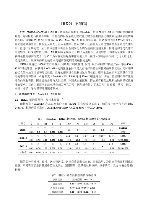
RF Coaxial Connectors
Introduction
The ITT Cannon range of 1.6/5.6 Connectors are suitable for use in 75 ohm communication systems. These connectors have become the recognised standard in telecommunication systems in many parts of the world. Designed to meet the requirements of DIN 47295, CECC 22240 and IEC 169-13, these connectors feature screw couplings to ensure mating integrity and snap coupling for ease of connection and disconnection (New Push-Pull coupling will be introduced in 1996). The range of parts shown in this publication includes plug and jack connectors for a variety of cables, together with PCB styles and U links. Other cable types and connector styles may be available on request.
protel 元件封装列表

Protel 99元件封装列表元件代号封装备注电阻R AXIAL0.3电阻R AXIAL0.4电阻R AXIAL0.5电阻R AXIAL0.6电阻R AXIAL0.7电阻R AXIAL0.8电阻R AXIAL0.9电阻R AXIAL1.0电容C RAD0.1方型电容电容C RAD0.2方型电容电容C RAD0.3方型电容电容C RAD0.4方型电容电容C RB.2/.4电解电容电容C RB.3/.6电解电容电容C RB.4/.8电解电容电容C RB.5/1.0电解电容保险丝FUSE FUSE二极管D DIODE0.4IN4148 二极管D DIODE0.7IN5408 三极管Q T0-126三极管Q TO-33DD15 三极管Q T0-663DD6 三极管Q TO-220TIP42 电位器VR VR1电位器VR VR2电位器VR VR3电位器VR VR4电位器VR VR5元件代号封装备注插座CON2 SIP2 2脚插座CON3 SIP3 3插座CON4 SIP4 4插座CON5 SIP5 5插座CON6 SIP6 6插座CON16 SIP16 16插座CON20 SIP20 20整流桥堆D D-37R 1A直角封装整流桥堆D D-38 3A四脚封装整流桥堆D D-44 3A直线封装整流桥堆D D-46 10A四脚封装集成电路U DIP8(S) 贴片式封装集成电路U DIP16(S) 贴片式封装集成电路U DIP8(S) 贴片式封装集成电路U DIP20(D) 贴片式封装集成电路U DIP4 双列直插式集成电路U DIP6 双列直插式集成电路U DIP8 双列直插式集成电路U DIP16 双列直插式集成电路U DIP20 双列直插式集成电路U ZIP-15H TDA7294集成电路U ZIP-11H1. 标准电阻:RES1、RES2;封装:AXIAL-0.3到AXIAL-1.0两端口可变电阻:RES3、RES4;封装:AXIAL-0.3到AXIAL-1.0三端口可变电阻:RESISTOR TAPPED,POT1,POT2;封装:VR1-VR52.电容:CAP(无极性电容)、ELECTRO1或ELECTRO2(极性电容)、可变电容CAPVAR封装:无极性电容为RAD-0.1到RAD-0.4,有极性电容为RB.2/.4到RB.5/1.0.3.二极管:DIODE(普通二极管)、DIODE SCHOTTKY(肖特基二极管)、DUIDE TUNNEL(隧道二极管)DIODE VARCTOR(变容二极管)ZENER1~3(稳压二极管)封装:DIODE0.4和DIODE 0.7;(上面已经说了,注意做PCB时别忘了将封装DIODE的端口改为A、K)4.三极管:NPN,NPN1和PNP,PNP1;引脚封装:TO18、TO92A(普通三极管)TO220H(大功率三极管)TO3(大功率达林顿管)以上的封装为三角形结构。
RC4559中文资料
POST OFFICE BOX 655303 • DALLAS, TEXAS 75265V IO Input offset voltage V O = 0V O = 0V O = 0mV nA nAI IO Input offset current I IB Input bias currentV IInput voltage range V/mVRC4559DUAL HIGH-PERFORMANCE OPERATIONAL AMPLIFIERPOST OFFICE BOX 655303 •DALLAS, TEXAS 75265元器件交易网元器件交易网IMPORTANT NOTICETexas Instruments and its subsidiaries (TI) reserve the right to make changes to their products or to discontinueany product or service without notice, and advise customers to obtain the latest version of relevant informationto verify, before placing orders, that information being relied on is current and complete. All products are soldsubject to the terms and conditions of sale supplied at the time of order acknowledgement, including thosepertaining to warranty, patent infringement, and limitation of liability.TI warrants performance of its semiconductor products to the specifications applicable at the time of sale inaccordance with TI’s standard warranty. Testing and other quality control techniques are utilized to the extentTI deems necessary to support this warranty. Specific testing of all parameters of each device is not necessarilyperformed, except those mandated by government requirements.CERTAIN APPLICATIONS USING SEMICONDUCTOR PRODUCTS MAY INVOLVE POTENTIAL RISKS OFDEATH, PERSONAL INJURY, OR SEVERE PROPERTY OR ENVIRONMENTAL DAMAGE (“CRITICALAPPLICATIONS”). TI SEMICONDUCTOR PRODUCTS ARE NOT DESIGNED, AUTHORIZED, ORWARRANTED TO BE SUITABLE FOR USE IN LIFE-SUPPORT DEVICES OR SYSTEMS OR OTHERCRITICAL APPLICATIONS. INCLUSION OF TI PRODUCTS IN SUCH APPLICATIONS IS UNDERSTOOD TOBE FULLY AT THE CUSTOMER’S RISK.In order to minimize risks associated with the customer’s applications, adequate design and operatingsafeguards must be provided by the customer to minimize inherent or procedural hazards.TI assumes no liability for applications assistance or customer product design. TI does not warrant or representthat any license, either express or implied, is granted under any patent right, copyright, mask work right, or otherintellectual property right of TI covering or relating to any combination, machine, or process in which suchsemiconductor products or services might be or are used. TI’s publication of information regarding any thirdparty’s products or services does not constitute TI’s approval, warranty or endorsement thereof.Copyright © 1998, Texas Instruments Incorporated。
NRF9E5中文资料
表 3 SFR 存储器映射表 1.2 PWM
nRF9E5 有一个可编程脉宽调制输出,它是 P0.7 的复用脚。PWM 可通过编程设置成 6,7,8 位脉宽 调制。占空比通过设置一个 8 位寄存器可设置在 0%和 100%间。 1.3 SPI
nRF9E5 以 SPI 接口控制为特点。SPI 的 3 根数据线(MISO,SCK 和 MOSI)具有多种复用功能。SPI 硬件不产生片选择信号。设计人员可以通过 GPIO 来设置一个或多个外部 SPI 的片选。EECSN 引脚是通用 I/O 接口,它在这里作为导入 EEPROM 的片选端。
应用领域:
无线数据通讯 报警和安全系统 自动测试系统 家庭自动化控制 遥控装置 监测 车辆安全系统 工业控制 无线通信 电信终端
适合高频应用
载波检测功能
低供电电流,发射时的典型值为 11mA@-10dBm,接收的典型值为 12.5mA
概述: nRF9E5是真正的系统级无线射频收发芯片,内嵌高性能8051MCU,4通道12位ADC。内置nRF905收
片内微控制器的指令周期为 4 到 20 个时钟周期,8051 为 12 到 48 个时钟周期。中断控制器支持 5 个扩展 中断源:ADC 中断, SPI 中断, 两个无线收发中断、一个唤醒中断。微控制器内有 3 个与 8052 相同的 定时器。一个与 8051 相同的串行通讯端口 UART。 CPU 备有两个数据指针,使得片外 RAM 存取数据变 得更为方便。系统时钟频率由晶体振荡器提供。 1.1. 1 存储器结构
AT89C51中文资料

A T89C51中文资料A T89C51是美国A TMEL公司生产的低电压,高性能CMOS8位单片机,片内含4k bytes的可反复擦写的只读程序存储器(PEROM)和128 bytes的随机存取数据存储器(RAM),器件采用A TMEL公司的高密度、非易失性存储技术生产,兼容标准MCS-51指令系统,片内置通用8位中央处理器(CPU)和Flash存储单元,功能强大A T89C51单片机可为您提供许多高性价比的应用场合,可灵活应用于各种控制领域。
主要性能参数:·与MCS-51产品指令系统完全兼容·4k字节可重擦写Flash闪速存储器·1000次擦写周期·全静态操作:0Hz-24MHz·三级加密程序存储器·128×8字节内部RAM·32个可编程I/O口线·2个16位定时/计数器·6个中断源·可编程串行UART通道·低功耗空闲和掉电模式功能特性概述:A T89C51提供以下标准功能:4k字节Flash闪速存储器,128字节内部RAM,32个I/O口线,两个16位定时/计数器,一个5向量两级中断结构,一个全双工串行通信口,片内振荡器及时钟电路。
同时,A T89C51可降至0Hz的静态逻辑操作,并支持两种软件可选的节电工作模式。
空闲方式停止CPU的工作,但允许RAM,定时/计数器,串行通信口及中断系统继续工作。
掉电方式保存RAM中的内容,但振荡器停止工作并禁止其它所有部件工作直到下一个硬件复位。
A T89C51方框图引脚功能说明·Vcc:电源电压·GND:地·P0口:P0口是一组8位漏极开路型双向I /O 口,也即地址/数据总线复用口。
作为输出口用时,每位能吸收电流的方式驱动8个TTL 逻辑门电路,对端口写“1”可作为高阻抗输入端用。
在访问外部数据存储器或程序存储器时,这组口线分时转换地址(低8位)和数据总线复用,在访问期间激活内部上拉电阻。
AT89C51RD2-IM中文资料
AT89C51RD2 / AT89C51ED2 QualPack Qualification PackageAT89C51ED2FLASH 8-bit C51 Microcontroller64 Kbytes FLASH, 2 Kbytes EEPROMAT89C51RD2 / AT89C51ED2JULY 2003AT89C51RD2 / AT89C51ED2 QualPack 1 Table of contents1TABLE OF CONTENTS (2)2GENERAL INFORMATION (3)3TECHNOLOGY INFORMATION (4)3.1W AFER P ROCESS T ECHNOLOGY (4)3.2P RODUCT D ESIGN (5)3.3D EVICE CROSS SECTION (6)4QUALIFICATION (7)4.1Q UALIFICATION M ETHODOLOGY (7)4.2Q UALIFICATION T EST M ETHODS (8)4.3W AFER L EVEL R ELIABILITY (9)4.3.1Electromigration (9)4.3.2Hot Carriers Injection (11)4.3.3Time Dependent Dielectric Breakdown (12)4.3.4FLASH Characteristics (14)4.4D EVICE R ELIABILITY (18)4.4.1Operating Life Testing (18)4.4.2ESD / Latch-up (18)4.4.3FLASH and EEPROM Data Retention and Endurance Cycling (18)4.4.4AT89C51ED2 Operating Reliability Calculation (20)4.5AT89C51ED2 P ACKAGING RELIABILITY (21)4.6AT89C51ED2 Q UALIFICATION STATUS (21)5ENVIRONMENTAL INFORMATION (22)6OTHER DATA (23)6.1ISO / TS16949 : 2002 C ERTIFICATE (23)6.2D ATA B OOK R EFERENCE (24)6.3R EVISION H ISTORY (24)AT89C51RD2 / AT89C51ED2 QualPack 2 General InformationProduct Name: AT89C51RD2Function: 8-bit Microcontroller with 64 Kbytes FLASHSPI InterfaceProduct Name: AT89C51E2Function: 8-bit Microcontroller with 64 Kbytes FLASH, 2 Kbytes EEPROMSPI InterfaceWafer Process: Logic CMOS 0.35 um with embedded FLASHAvailable Package Types PLCC 44, VQFP 44, PLCC 68, VQFP 68 ,PDIL 40Other Forms: Die, WaferLocations:Process Development, Atmel Colorado Springs, USAProduct Development Atmel Nantes, FranceWafer Plant Atmel Colorado Springs, USAQC Responsibility Atmel Nantes, FranceProbe Test Atmel Colorado Springs, USAAssembly Depending on packageFinal Test Atmel TSTI Manila, PhilippinesLot Release Atmel Nantes, FranceShipment Control Global Logistic Center, PhilippinesQuality Assurance Atmel Nantes, FranceReliability Testing Atmel Nantes, FranceFailure Analysis Atmel Nantes, FranceQuality ManagementAtmel Nantes, FranceSigned: Pascal LECUYERAT89C51RD2 / AT89C51ED2 QualPack 3 Technology Information3.1 Wafer Process TechnologyProcess Type (Name): Logic 0.35um with embedded FLASH (AT56800)Base Material: Epitaxied SiliconWafer Thickness (final) 475 umWafer Diameter 150 mmNumber Of Masks 27Gate Oxide (Logic transistors)Material Silicon DioxideThickness 68AGate Oxide (EPROM cell)Material Silicon DioxideThickness 390APolysiliconNumber of Layers 2Thickness Poly 1 1400A AmorphousThickness Poly 2 3200AMetalNumber of Layers 3Material: Aluminum CopperLayer 1 Thickness 5000ALayer 2 Thickness 5000ALayer 3 Thickness 8000APassivationMaterial Oxide HDP/ Oxy-nitrideThickness 21000AAT89C51RD2 / AT89C51ED2 QualPack 3.2 Product DesignDie Size 17,9 mm2Pad Size Opening / Pitch 66 um * 66 um / 111 umLogic Effective Channel Length 0.35 µmGate Poly Width (min.) 0.35 µmGate Poly Spacing (min.) 0.42 µmMetal 1 Width 0.42 µmMetal 1 Spacing 0.49 µmMetal 2 Width 0.56 µmMetal 2 Spacing 0.49 µmMetal 3 Width 0.56 µmMetal 3 Spacing 0.49 µmContact Size 0.35 µmContact Spacing 0.42 µmVia 1 Size 0.42 µmVia 2 Size 0.42 µmRev. 0 – 2003 July 5AT89C51RD2 / AT89C51ED2 QualPack 3.3 Device cross sectionAT56Kxx cross sectionAT89C51RD2 / AT89C51ED2 QualPack 4 Qualification4.1 Qualification MethodologyAll product qualifications are split into three distinct steps as shown below. Before a product is released for use, successful qualification testing are required at wafer, device and package level.- Wafer Level Reliability consists in testing individually basic process modules regarding their well known potential limitations (Electro-migration, Hot Carriers Injection, Oxide Breakdown, NVM Data Retention).Each test is performed using wafer process specific structures.- Device reliability is covering either dice design and processing aspects. The tests are performed on device under qualification, but generic data may also be considered for reliability calculation.- For each package type proposed in the Datasheet, it is verified that qualification data are available. If not qualification tests are carried out for the new package types. In addition, one package type is selected to verify packaging reliability of the device under qualification.AT89C51RD2 / AT89C51ED2 QualPack 4.2 Qualification Test MethodsGeneral Requirements for Plastic packaged CMOS ICs:Standard Test Description AcceptanceMIL-STD 883 Method 1005 Electrical Life Test (Early Failure Rate)48 hours 140°C0/300 - 48hMIL-STD 883 Method 1005 Electrical Life Test (Latent Failure Rate)1000 hours 140°C Dynamic or Static0/100 - 500hMIL-STD 883 Method 3015.7Electrostatic Discharge HBM+/-2000v 1.5kOhm/100pF/3 pulses0/3 per levelJEDEC 78 Latch up50mW power injection, 50% overvoltage @125°C0/5 per stressAEC Q100 Method 005NVM EnduranceProgram Erase Cycles 25°C0/50 - 10kcAEC Q100 Method 005NVM Data RetentionHigh Temperature Storage 165°C0/50 - 500hMIL-STD 883 Method 1010Temperature Cycling1000 cycles –65°C/150°C air/air0/50 - 500cAtmel PAQA0184 HAST after Preconditioning144 hours 130°C/85%RH0/50 – 96hEIA JESD22-A10185/85 Humidity Test1000 hours 85°C/85%RH0/50 - 500hEIA JESD22-A110HAST336 hours 130°C/85%RH0/50 - 168hEIA JEDEC 20-STDPreconditioningSoldering Stress 220°C/235°c/3 times0/11 per classMIL-STD 883Method 2003Solderability 0/3MIL-STD 883Method 2015Marking Permanency 0/5AT89C51RD2 / AT89C51ED2 QualPack 4.3 Wafer Level Reliability4.3.1 ElectromigrationPurpose:To evaluate the AT56800, AT35500, and AT37000 processes for Metal 1, Metal 3 &Via Electromigration Reliability. These 3 processes have the same steps for interconnect levels.Test Parameters:Metal 1 & Metal 3:Sample Size = 15Temp = 250C with Joule heating .J = 3.5E06 A/cm2.Via:Sample Size = 15Temp = 200C with Joule heating.J = 2.5E06 A/cm2.Black’s Equation Parameters:Failure Criteria - 10% increase in resistance. Data taken every 1% change.n = 2Ea = 0.6eVLifetime Predictions:Metal 1 :Split 1 - Tf.1% exp = ~ 28 hrs Tf.01% op = ~ 28 hrs x 39706 accel = 127 years.(Sigma = 2.7118 hours, Accel temp = 130, Accel current = 306)Metal 3 :Split 3 - Tf.1% exp = ~ 140 hrs Tf.01% op = ~ 140 hrs x 39706 accel = 634 years.(Sigma = 1.8782 hours, Accel temp = 130, Accel current = 306)VIA :Split 4 - Tf.1% exp = ~ 22 hrs Tf.1% op = ~ 22 hrs x 7144 accel = 18 years.(Sigma = 2.59 hours, Accel temp = 31.75, Accel current = 225) (9/15 fails)Conclusion:All splits pass the minimum 10 years lifetime.AT89C51RD2 / AT89C51ED2 QualPack Test results :AT56800 metal 1 results AT56800 metal 3 resultsAT56800 VIA resultsElectromigration summary table:Level SampleSizeFails @10%Tf.1%Lifetime (yrs)M1 15 9 140M3 15 7 1088Via 15 9 19AT89C51RD2 / AT89C51ED2 QualPack 4.3.2 Hot Carriers InjectionTest conditionsThe test is performed by forcing a high drain bias on the test device (Vds>Vddmax) to accelerate the carriers to the maximum. At the same time the gate bias (Vgs) is chosen in order to maximize the injection of carriers into the gate oxide and also the substrate. WLR_B n-channel W/L 0.35um/25um the stress is performed on a number of transistors, each at a different stress condition Vds,stress and Vgs,stress. For each transistor, the time to reach the failure criteria (dIdsat/Idsat=10%) is obtained. NMOS is more sensitive to hot carriers compared to PMOS. Consequently NMOS is the only structure tested.MeasurementAT568T7 lot 1J0433 has been measured using the WLR_B hot electron structure with standard drain.NMOS W/L = 25/0.35 um.ResultsConclusionThe extrapolated life time in the worst case conditions (@Vds=Vdd max & Vgs set to maximize substrate current) is much greater than 0.2 years in DC mode (qualification requirement) which is equivalent to more than 10 years in AC mode.AT89C51RD2 / AT89C51ED2 QualPack 4.3.3 Time Dependent Dielectric BreakdownPurpose:To evaluate the AT56800 thin gate oxide TDDB performance as follows:a) To determine the activation energy of gate oxide failures on STI active edge capacitorsb) To determine the field acceleration factor for intrinsic gate oxide failuresc) To determine the sigma the lognormal standard deviation of the time to breakdown distribution of theintrinsic gate oxideTest Parameters:Lot 9G3470 (wafers 4, 5, 18)Min thickness: 72.9AMax thickness: 74.7ACapacitor size: 6.267 um2The stress conditions used are shown below:Temperature/Field 9.5MV/cm 10.0MV/cm 10.5MV/cm225C N=5 N=5 N=5200C N=5 N=5 N=5175C N=5 N=5 N=6Accumulated total stress time: 132 hours / 46 capacitorsCalculation Parameters:Failure Criteria: 0.01% failuresTemp/Voltage use: 105°C / 3.3VOxide thickness: 63A (target –10%)Lifetime Prediction:The equation used to describe the breakdown of gate oxides is:Tbd(i) = exp(SIGMA*Z(i) + GAMMA*Eox +Ea/kT + T0)WhereTbd(i) is the time to breakdown of the i th capacitor,SIGMA is the lognormal standard deviation of the breakdown distribution,Z(i) is the Z-score of the i th capacitor (essentially the difference between its breakdown time and the mean measured in standard deviations),GAMMA is the Field acceleration constant,Eox is the oxide field,Ea is the activation energy of this failure mechanism,K is Boltzmann’s constant,T is the Kelvin Temperature, andT0 is a fitting constant.AT89C51RD2 / AT89C51ED2 QualPack The best fit coefficients in the regression analysis are:T0= 14.25034317 LN-secEa= 1.060043152 eVGAMMA= -3.2454227 LN-sec-cm/MVSIGMA= 0.414655753 LN-secwith an adjusted r-squared of 97.99%. The intrinsic lifetime at use conditions calculated from this regression is 56174 years.Conclusion:Using the coefficients determined above, the time to reach any cumulative percent failure level can be estimated given the stress conditions. Using 105C and 3.3 volts on 63 Angstrom N-Channel gate2 oxide, we may expect0.01% of capacitors having 6,267 square microns area with 6,174 microns of active edge to fail in about 613 years, exceeding the technology requirement of ten years.Test results :AT89C51RD2 / AT89C51ED2 QualPack 4.3.4 FLASH Characteristics4.3.4.1 Cell endurancePurpose:To evaluate the ability of memory cell to withstand high number of program/erase cycles without change of electrical characteristics.Test Parameters:Measurements have been done on lot 0R5414.Test done on 2 cells in a byte :- cell near byte select transistor, called bit0 (1st column)- cell near Vss contact, called bit 7 (8th column).Cycling is done for various programming voltages :- write : 13.5V on BL / 15.6V on select - clear : 13.5V on sense / 15.6V on select@5ms 14.5V on BL / 16.6V on select @5ms 14.5V on sense / 16.6V on select15.5V on BL / 17.6V on select 15.5V on sense / 17.6V on select16.5V on sense / 17.6V on selectAT89C51RD2 / AT89C51ED2 QualPack Conclusions:- Vt_wrt shift of 200 mV after 10k cycles- I_read decrease of 2.5 uA after 10kcycles (- 7 to 9 %)- No big difference between bit0 and bit 7 in terms of Vt or current variations Using the coefficients4.3.4.2 Cell retentionPurpose:To extrapolate cell life duration at 125°C from bake measurements at high temperature.Test parameters:Lot: 9T0930Temperature: 250°C and 200°CDuration: 92 hoursLifetime Prediction:The equation used to describe memory cell retention is:DVt (V) = A * (t[h])^m * exp (-1.05eV/kT[K])Results :Test measurements Extrapolated Life TimeConclusions :Extrapolation to 125°C - 10years = Vt loss is less than 0.8 mVAT89C51RD2 / AT89C51ED2 QualPack 4.3.4.3 Cell Read DisturbPurpose:To measure read disturb influence on 56k8 memory cell.Test parameters:Lot: 0t0348Programming: 14V on WL and sensegate @5msTemperature: 25°C and 140°CThe cell is stressed with BL voltage much higher than standard read conditions (around 6V) to accelerate disturb phenomenon : electrons from the Floating gate can move through the tunnel oxide. This charge loss is measured after stress by a Vt measurement.Test results:Conclusion:Extrapolation to 10 years lifetime give a maximum BL voltage of around 4V in read operation, which is much higher than nominal BL read voltage (~1V). So there is no sensitivity to read disturb either at room temperature or high temperature.AT89C51RD2 / AT89C51ED2 QualPack 4.3.4.4 Wafer probe Data retention measurementData retention has been verified after bake for 168 hours at 250°C on 3 wafers of a standard production lot. The results are summarized in the table below:Time to failureLot Wafer % Retention loss Failure rateextrapolation at 55°C1G4448 6 0% 3.91fit >> 10 years1G4448 8 0% 4.19fit >> 10 years1G4448 12 0% 3..96fit >> 10 yearsTotal 0% 1.34fit >> 10 years Conclusion:Data Retention measurements at wafer probe stand out high data retention capability of AT56800 products, exceeding the technology requirement of ten years.AT89C51RD2 / AT89C51ED2 QualPack 4.4 Device Reliability4.4.1 Operating Life TestingAT89C51ED2 test results are summarized in the table below.Lot Device Type Test Description Step Result CommentA01948K AT89C51ED2PLCC 44 EFR Dynamic Life Test 12h48h0/3000/300LFR Dynamic Life Test 500h1000h0/1000/1004.4.2 ESD / Latch-upAT89C51ED2 test results are summarized in the table below.Lot Device Type Test Description Step Result CommentA01948 AT89C51ED2PLCC 44 ESD-HBM Model 2000V3000V4000V5000V0/31/31/31/3Class 2 of MIL STD 883LATCH-UPOver-VoltagePower Injection5.5v50mW0/50/5Test done at 125°CClassified latch-up free4.4.3 FLASH and EEPROM Data Retention and Endurance CyclingAT89C51ED2 test results are summarized in the table below.Lot Device Type Test Description Step Result CommentA01948K AT89C51ED2PLCC 44 Data Retention 500h1000h0/500/50Program / EraseEndurance Cycling100kc 0/30 32k USER memoryProgram / EraseEndurance Cycling100kc 0/30 2k DATA memoryAT89C51RD2 / AT89C51ED2 QualPack AT56800 Program / Erase Endurance:Temperature acceleration factor calculation:AT56800 FLASH / EEPROM Reliability Calculation:Global Calculation AT56800MicrocontrollersData-Retention Test 165°c250°c0/11010000/251496For current sample sizeexpressed in device*hours,Ea = 0.7eV, CL = 60%, T = 55°:?DR= 0.29 fitEndurance Cycling 55°c 1/109850k Failure : 1 bit charge lossFor sample size expressed inequivalent cycles at 55°c, andassuming one cycle per day,Ea = 0.25eV, CL = 60%:?EC= 0.76 fitAT89C51RD2 / AT89C51ED2 QualPack4.4.4 AT89C51ED2 Operating Reliability CalculationIn the next table, it is proposed a AT89C51ED2 reliability prediction calculated at 55°c for 60% confidence level from generic test data collected over the 12 last months process monitor.Lots Device Type Test Description Step Result CommentA00648 P01709 A00988B T89C51CC01VQFP 44EFR Dynamic Life Test 48h 0/3787A01459AA01460EA01615BLFR Dynamic Life Test 1000h 0/266A01110C A01110D T89C51CC02SOIC28EFR Dynamic Life Test 48h 1/1260 1 Ipd drift caused by scratch onmetal 1A01185FA01366ELFR Dynamic Life Test 1000h 0/280A01679A A01679B T89C51RC2PLCC 44EFR Dynamic Life Test 48h 0/1856LFR Dynamic Life Test 1000h 0/100A00808A A00943E T89C51RB2PLCC 44EFR Dynamic Life Test 48h 0/300LFR Dynamic Life Test 1000h 0/100A01487Q A02179 T85C5121T89C5121EFR Dynamic Life Test 48h 0/684 SSOP24 LFR Dynamic Life Test 1000h 0/100A01435H A01435K AT89C5114SOIC20EFR Dynamic Life Test 48h 0/1887A02293C LFR Dynamic Life Test 1000h 0/200A00960C A01808A AT89C51SND1AT83C51SND1EFR Dynamic Life Test 48h 1/550 Consumption hot spot in DCLKinput bufferA01914J VQFP 80 LFR Dynamic Life Test 1000h 0/170A01584A AT89C5131VQFP64EFR Dynamic Life Test 48h 0/350LFR Dynamic Life Test 1000h 0/100Global EFR Dynamic Life Test 48h 2/10674 187 ppmLFR Dynamic Life Test - 0/1316 4.4 fitAT89C51RD2 / AT89C51ED2 QualPack4.5 AT89C51ED2 Packaging reliabilityIn this section are presented the packaging qualification measurements carried out in PLCC 44.Lots Device Type Test Description Step Result CommentA01948K AT89C51ED2PLCC 44 Humidity 85/85 postPreconditioning level 1500h 0/500/50Thermal Cycles postPreconditioning L1500c1000c0/500/50Autoclave post thermalshocks and Precond. L196h 0/50A01679C AT89C51RC2PLCC44 Preconditioning level 1 SAMVisualElect.0/110/500/50 Thermal Cycles postPreconditioning L1500c1000c0/500/50Humidity 85/85 postPreconditioning level 1500h 0/500/50Autoclave post thermalshocks and Precond. L196h 0/50High TemperatureStorage500h1000h0/500/50 Marking permanency Visual 0/54.6 AT89C51ED2 Qualification statusAtmel digital 0.35 um wafer process is qualified since 1999, October.Derived from this technology, AT89C51RD2 / AT89C51ED2 have passed successfully Reliability Testing. Full qualification has been pronounced in June 2003.All package pass Level 1 of Moisture Sensitivity Ranking as per JESD 20B. Therefore, Dry Packing is not mandatory.AT89C51RD2 / AT89C51ED2 QualPack5 Environmental InformationAtmel Nantes Environmental Policy aims are :- Reducing the use of harmful chemicals in its processes- Reducing the content of harmful materials in its products- Using re-usable materials wherever possible- Reducing the energy content of its productsAs part of that plan, Ozone Depleting Chemicals are being replaced either by Atmel Nantes or its sub-contractors. Atmel Nantes site is ISO14001 certified since May 2000.AT89C51RD2 / AT89C51ED2 QualPack 6 Other Data6.1 ISO / TS16949 : 2002 CertificateAT89C51RD2 / AT89C51ED2 QualPack6.2 Data Book ReferenceThe data sheet is available upon request to sales representative or upon direct access on Atmel web site:/Address ReferencesAll inquiries relating to this document should be addressed to the following:Atmel NantesBP7060244306 Nantes Cedex 3FranceTelephone (33) 2 40 18 18 18Telefax (33) 2 40 18 19 00Or direct contactPascal LECUYERTelephone (33) 2 40 18 17 73Telefax (33) 2 40 18 19 466.3 Revision HistoryIssue Modification Notice Application Date0 Initial Product Evaluation 2003 JulyRemarks:The information given in this document is believed to be accurate and reliable. However, no responsibility is assumed by Atmel for its use. No specific guarantee or warranty is implied or given by this data unless agreed in writing elsewhere.Atmel reserves the right to update or modify this information without notification, at any time, in the interest of providing the latest information.Parts of this publication may be reproduced without special permission on the condition that our author and source are quoted and that two copies of such extracts are placed at our disposal after publication. Before use of such reproduced material the user should check that the information is current.Written permission must be obtained from the publisher for complete reprints or translations。
- 1、下载文档前请自行甄别文档内容的完整性,平台不提供额外的编辑、内容补充、找答案等附加服务。
- 2、"仅部分预览"的文档,不可在线预览部分如存在完整性等问题,可反馈申请退款(可完整预览的文档不适用该条件!)。
- 3、如文档侵犯您的权益,请联系客服反馈,我们会尽快为您处理(人工客服工作时间:9:00-18:30)。
Information furnished by HAMAMATSU is believed to be reliable. However, no responsibility is assumed for possible inaccuracies or omissions. Specifications are subject to change without notice. No patent rights are granted to any of the circuits described herein. ©1999 Hamamatsu Photonics K.K
Subject to local technical requirements and regulations, availability of products included in this promotional material may vary. Please consult with our sales office.GENERAL
Parameter
Description/Value
Unit Spectral Response
Wavelength of Maximum Response
Photocathode
Window Dynode
Base
Suitable Socket
nm nm —mm dia.—————
400 to 930
550Multialkali
50Fiber optic Box-and-grid
10
14-pin base JEDEC No. B14-38
E678-14A (supplied)
Material
Minimum Effective Area
Material
Structure
Number of Stages
PHOTOMULTIPLIER TUBES
R4519, R4519-01
MAXIMUM RATINGS (Absolute Maximum Values)
Supply Voltage: 1000 V dc, K: Cathode, Dy: Dynode, P: Anode
Do not cooled the R4519 to lower than -30 °C. The fixing glue of the base may cause cracking in the glass bulb.
Use the R4519-01 instead. The voltage divider should be assembled on a PC board or similar with at least 5 to 10 mm apart from the PMT stem.
Extended Red Multialkali Photocathode Fiber Optic Faceplate, 10-Stage, Head-on
CHARACTERISTICS (at 25 °C)
VOLTAGE DISTRIBUTION RATIO AND SUPPLY VOLTAGE
Parameter
Min.Unit Parameter
Value Unit Supply Voltage Average Anode Current Ambient Temperature
15002500.1
-30 to +50 (R4519) -80 to +50 (R4519-01)
Vdc Vdc mA °C
Between Anode and Cathode Between Anode and Last Dynode
Cathode Sensitivity
Anode Sensitivity Gain
Anode Dark Current (after 30 min. storage in darkness)
Time Response
Electrode Ratio K G Dy1Dy21Dy31Dy41Dy51Dy61Dy71Dy81Dy9Dy10111P Luminous (2856K)
Quantum Efficiency at 850 nm Red / White Ratio (with R-68 filter)Luminous (2856K)
Anode Pulse Rise Time
Electron Transit Time
200—0.4520————
27030.52007.4 × 105
40970
µA/lm %—A/lm —nA ns ns
—————200——
Typ.Max.11
PHOTOMULTIPLIER TUBES R4519, R4519-01
Figure 1: Typical Spectral Response
TPMH1269E01NOV. 1999 IP
Figure 2: Dimensional Outline and Basing Diagram (Unit: mm)
R4519
R4519-01
TPMHA0462EA
TPMHA0461EA
HAMAMATSU PHOTONICS K.K., Electron Tube Center
314-5, Shimokanzo, Toyooka-village, Iwata-gun, Shizuoka-ken, 438-0193, Japan, Telephone: (81)539/62-5248, Fax: (81)539/62-2205
U.S.A.: Hamamatsu Corporation: 360 Foothill Road, P. O. Box 6910, Bridgewater. N.J. 08807-0910, U.S.A., Telephone: (1)908-231-0960, Fax: (1)908-231-1218
Germany: Hamamatsu Photonics Deutschland GmbH: Arzbergerstr. 10, D-82211 Herrsching am Ammersee, Germany, Telephone: (49)8152-375-0, Fax: (49)8152-2658
France: Hamamatsu Photonics France S.A.R.L.: 8, Rue du Saule Trapu, Parc du Moulin de Massy, 91882 Massy Cedex, France, Telephone: (33)1 69 53 71 00, Fax: (33)1 69 53 71 10
United Kingdom: Hamamatsu Photonics UK Limited: Lough Point, 2 Gladbeck Way, Windmill Hill, Enfield, Middlesex EN2 7JA, United Kingdom, Telephone: 44(20)8-367-3560, Fax: 44(20)8-367-6384North Europe: Hamamatsu Photonics Norden AB: Smidesvägen 12, SE-171-41 SOLNA, Sweden, Telephone: (46)8-509-031-00, Fax: (46)8-509-031-01Italy: Hamamatsu Photonics Italia: S.R.L.: Strada della Moia, 1/E, 20020 Arese, (Milano), Italy, Telephone: (39)02-935 81 733, Fax: (39)02-935 81 741
HOMEPAGE URL
10-2
10-1
100
101
102
C A T H O
D
E R A D I A N T S E N S I T I V I T Y (m A /W )Q U A N T U M E
F F
I C I E N C Y (%)
WAVELENGTH (nm)
DY4
P。