PCB电路板术语
pcb常用的专业术语
pcb常用的专业术语PCB常用的专业术语PCB,即印刷电路板,是电子产品中不可或缺的一部分。
在PCB制造过程中,有许多专业术语需要了解。
本文将从材料、工艺、设计等方面介绍PCB常用的专业术语。
一、材料1.基板(Substrate)基板是指印刷电路板上的主体部分,通常由玻璃纤维和树脂复合材料构成。
基板的质量直接影响着整个PCB的性能。
2.铜箔(Copper Foil)铜箔是印刷电路板上最重要的导电层材料,其厚度通常为18um至105um之间。
铜箔的质量和厚度对于PCB的导电性能和可靠性有着重要影响。
3.覆铜板(Copper Clad Board)覆铜板是指在基板表面涂覆一层铜箔而成,通常有单面、双面和多层三种形式。
不同类型的覆铜板适用于不同种类的电路设计需求。
4.阻焊(Solder Mask)阻焊是一种涂在印刷电路板上以保护未焊接区域免受污染和短路的材料。
阻焊通常为绿色、红色或蓝色,具有良好的耐高温性和化学稳定性。
5.沉金(ENIG)沉金是一种表面处理技术,可以在印刷电路板上形成一层金属保护层,提高PCB的可靠性和耐腐蚀性。
沉金通常用于高端PCB产品中。
二、工艺1.蚀刻(Etching)蚀刻是印刷电路板制造中最重要的工艺之一,其目的是去除不需要的铜箔以形成电路图案。
蚀刻过程需要使用化学溶液和光敏树脂等材料。
2.钻孔(Drilling)钻孔是指在印刷电路板上钻洞以安装元器件或连接不同层之间的导线。
钻孔需要使用高速钻头和自动化设备完成。
3.压合(Lamination)压合是指将多个覆铜板通过热压技术粘合在一起形成多层PCB结构。
压合过程需要控制温度、压力和时间等参数,确保PCB质量符合要求。
4.喷锡(Soldering)喷锡是一种表面处理技术,可以在印刷电路板上形成一层锡保护层,提高PCB的可靠性和耐腐蚀性。
喷锡通常用于中端PCB产品中。
5.贴片(SMT)贴片是指将元器件直接安装在印刷电路板上的一种技术。
PCB专业术语大汇集
PCB专业术语大汇集PCB专业术语大汇集PCB是Printed Circuit Board的缩写,即印制电路板。
作为现代电子制造中不可或缺的一个组成部分,PCB技术已经成为电子制造的核心技术之一。
如果你在PCB制造领域工作或学习,那么理解并熟练掌握一些常见的PCB专业术语是非常重要的。
在这篇文章中,我们将罗列一些重要的PCB专业术语和技术名词,以帮助大家更好地理解PCB的制造和设计。
一、PCB制造基础1. PAD:焊盘,指印制电路板上用于焊接元器件的金属区域。
2. VIA:通孔,指在印制电路板上打开的金属通孔,连接不同层之间的电路。
3. Solder mask:焊膜,是一种覆盖在PCB表面的保护层,用于防止无意中的短路和腐蚀。
4. Silk screen:丝印,是印刷在印制电路板上的文字和图像,用于标记焊点、元器件和引脚等信息。
5. Cooper:铜箔,是一种用于制造PCB的材料。
6. Substrate:衬底,指PCB中负责固定和支撑电路的材料。
7. Copper weight:铜厚度,指PCB上铜箔的厚度,单位是oz。
8. Panel:板子,指PCB制造中一组连续的PCB,通常需要在单个板子上打印多个电路。
9. Plating:镀,指将金属材料沉积在印制电路板表面或内部的过程。
10. Tolerance:公差,指PCB制造和设计中可以接受的误差范围。
二、PCB设计技术1. Trace:走线,指印制电路板上的导线,用于连接不同的元器件和电路板上的不同部分。
2. Clearance:间隙,指PCB上不同元器件或电路之间的距离。
3. Net:网络,指一个电路的连接点集合,通常用来描述PCB上的一组连通电路。
4. Gerber:杰伯,是一种文件格式,通常用于将PCB设计转化为PCB生产所需的制造文件。
5. Footprint:插件,指印制电路板上元器件焊盘的设计,用于确保元器件和焊盘正确对齐和正确连接。
pcb专业术语英文及翻译
pcb专业术语英文及翻译摘要:本文介绍了PCB(Printed Circuit Board,印刷电路板)专业术语的英文表达和翻译,根据内容实际需求分为三大类:PCB制造术语、PCB组装术语和PCB测试术语。
在每个类别下,将列举相关术语及其英文表达和翻译,从而帮助读者更好地理解和运用PCB专业术语。
正文:I. PCB制造术语1. 单、双面板 (Single-sided, Double-sided board)单面板:一种仅在板的一侧进行布线和元件安装的印刷电路板。
双面板:一种在两侧布线和元件安装的印刷电路板。
2. 环氧树脂 (Epoxy Resin)环氧树脂是一种常用的PCB基材,具有良好的绝缘性和耐热性。
3. 铜盖膜 (Copper Foil)铜盖膜是覆盖在印刷电路板表面的一层铜箔,用于电气连接。
4. 阻焊层 (Solder Mask Layer)阻焊层是一种覆盖在印刷电路板表面的保护层,用于防止元件的误焊。
5. 玻璃纤维布 (Glass Fiber Cloth)玻璃纤维布是PCB制造中一种常用的增强材料,用于提高印刷电路板的强度和耐磨性。
6. 焊盘 (Pad)焊盘是印刷电路板上用于连接元件引脚的焊接区域。
7. 过孔 (Through-hole)过孔是印刷电路板上贯穿两侧的孔洞,用于连接不同电子元器件。
8. 排针 (Pin Header)排针是一种插针式连接器,常用于将PCB与其他设备连接。
9. 焊接 (Soldering)焊接是将电子元件与印刷电路板焊接在一起的一种连接方法。
II. PCB组装术语1. 表面贴装技术 (Surface Mount Technology, SMT)表面贴装技术是一种将电子元件直接焊接在印刷电路板表面的组装方法。
2. 波峰焊接 (Wave Soldering)波峰焊接是一种通过将印刷电路板浸入焊锡浪涌中来实现电子元件的连接。
3. 焊接膏 (Solder Paste)焊接膏是表面贴装技术中使用的一种黏性材料,用于在印刷电路板上确定元件的位置并进行焊接。
PCB专业用语中英文对照

PCB专业用语中英文对照PCB,全称是Printed Circuit Board,即印制电路板,是电子器件中不可缺少的一部分。
在PCB的生产和使用过程中,有许多特定的专业术语,以下将列出一些常见的PCB专业用语的中英文对照,以帮助PCB行业的从业人员更好地了解和使用这些术语。
1. Pad - 表面贴装元件引脚焊盘2. Via - 通孔3. Trace - 线路走线4. Solder mask - 焊盘阻焊5. Silkscreen - 字体绘制6. Substrate - 基板7. RoHS - 过度有害物质限制指令8. PCB Assembly - PCB组装9. Panel - 夹板10. Gerber file - Gerber文件(PCB板图文件的一种)11. Copper weight - 铜箔厚度12. SMD - 表面贴装元件13. Through-hole - 贯通孔除此之外,还有一些专业用语需要注意:1. Blind via - 盲孔2. Buried via - 埋孔3. Soldering - 焊接4. Copper pour - 铜泡5. Annular ring - 环形垫片6. Plated through-hole - 化学镀铜孔7. Gold finger - 金手指(PCB板边部的带触点金属部件)8. OSP - 有机锡防护(一种PCB表面处理方法)以上仅列举了部分PCB专业用语的中英文对照,如需更全面的了解,需要从事相关行业或有专业经验的人士掌握更多知识。
在PCB制造和使用过程中,正确使用这些专业用语是非常重要的,它们不仅可以帮助我们更好地了解PCB的生产过程和使用方法,还可以提高工作效率和避免出现误解和错误。
PCB电路板术语
PCB电路板术语-钻孔、成型作业1、Algorithm 算法(钻孔、成型作业)在各种计算机数值操控(CNC,Computer Numerical Control)的设备中,其软件有限指令的集合体,称为"算法"。
可用以执行简单的机械动作,如钻孔的呆板严谨的程或(Program)即根据某一算法所写出的。
算法需满足五要素:(1)输入可有可无,(2)至少一个输出,(3)每个指令清晰明确定义,(4)执行需在有限步骤内结束,(5)每个指令需可由人仅用笔和纸执行。
2、Back Taper 反锥斜角(钻孔、成型作业)指钻针自其尖部向柄部延伸之主干上,其外缘之投影稍呈现头大尾小之外形,如此将可减少钻针外表与孔壁的摩擦面积。
此一反斜角称为 Back Taper ,其角度约1~2°之间。
3、Back﹣up 垫板(钻孔、成型作业)是钻孔时垫在电路板下,与机器台面直接接触的垫料,可避免钻针伤及台面,并有降低钻针温度,清除退屑沟中之废屑,及减少铜面出现毛头等功用。
一般垫板可采酚醛树脂板或木浆板为原料。
4、Bevelling 切斜边(钻孔、成型作业)指金手指的接触前端,为方便进出插座起见,特将其板边两面的直角缘线削掉,使成 30~45℃ 的斜角,这种特定的动作称为 "切斜边"。
5、Bits 头(钻孔、成型作业)指各种金属工具可替换之尖端,例如钻针(头)Drill Bits,板子外形成形用的旋切头 Rounting Bits,或烙铁头 Solder Iron Bits 等。
6、Blanking 冲空断开(钻孔、成型作业)利用冲模方式,将板子中央无用的部份予以冲掉。
7、Burrr 毛头(钻孔、成型作业)在 PCB 中常指钻孔或切外形时,所出现的机械加工毛头即是。
偶而也用以表达电镀层之粗糙情形。
8、Carbide 碳化物(钻孔、成型作业)在 PCB 工业中,此字最常出现在钻孔所用的钻针(头)上,这种耗材的主要成份为"碳化钨Tungsten Carbide (WC),约占94%,其余6%为金属钴粉(当成黏结)。
PCB电路板术语
PCB电路板术语电路板是一种重要的电子元器件,主要用于连接电子元器件并传输电信号。
PCB电路板术语是PCB制造中常用的技术术语的总称,本文将介绍一些基本的PCB电路板术语。
一、PCBPCB是印制电路板的缩写,它是电子设备中的重要组成部分。
PCB是基于导电材料(如铜)和一种绝缘材料(通常是FR-4)的板式结构,通过打孔和逐层聚合形成的复杂电路。
PCB有许多种不同的类型和结构,根据需要可以选择最合适的类型。
二、Gerber文件Gerber文件是PCB制造过程中不可或缺的文件之一。
Gerber文件包含有关PCB电路板的重要参数,如元件位置、距离、孔位置等。
Gerber文件可以被PCB制造工厂使用,用来制造出最终的电路板。
三、BOMBOM是制造产品所需的所有材料的清单。
在PCB制造中,BOM包括原材料、电子元件和其他组件,如螺丝和连接器等。
BOM是PCB制造和组装中的重要文档,可以确保PCB制造过程中使用的所有材料和元件的可追溯性。
四、PCBAPCBA是印制电路板组装的缩写,它是将电子元器件焊接到PCB上的过程。
PCBA制造一般包括贴片和穿孔两种工艺。
1.贴片:贴片是将表面贴装元件直接固定在PCB的表面。
这种工艺可以提高制造效率,并减少生产成本,但需要使用高精度仪器。
2.穿孔:穿孔技术是将元件的引脚穿过PCB的孔中并固定在板子的反面。
这种技术通常用于连接较大的元件或较厚的电线。
五、PTH和NPTHPTH代表“穿越孔”,是一种在PCB上穿孔的方法,用于穿过板的电气连接。
NPTH代表“非穿越孔”,不会跨过整个电路板,通常用于连接连接器或装置到电路板上。
六、层在PCB制造中,一件PCB一般都由许多层组成。
PCB层数通常都以偶数为主,常用的层数为2层、4层、6层、8层、10层和12层等。
每层都用不同的颜色来表示。
七、SMTSMT代表“表面贴装技术”,是一种高效的电子元件连接方式。
SMT将电子元件直接贴在PCB表面,省去了通过PCB穿孔的过程,大大提高了制造效率和减少了体积。
PCB电路板术语
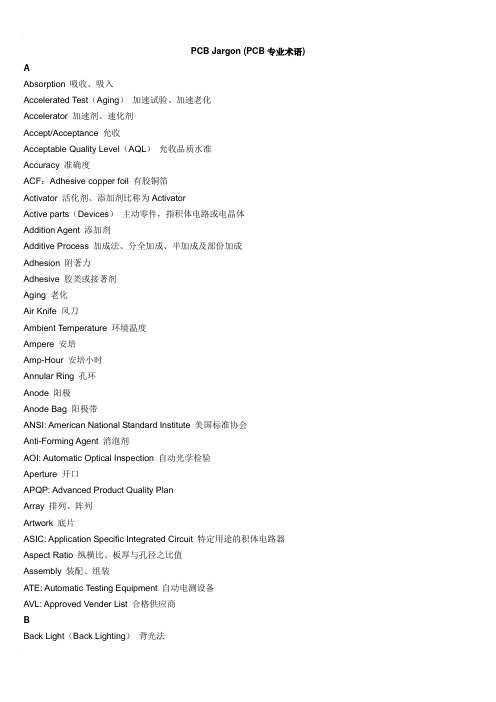
PCB Jargon (PCB专业术语) AAbsorption 吸收、吸入Accelerated Test(Aging)加速试验、加速老化Accelerator 加速剂、速化剂Accept/Acceptance 允收Acceptable Quality Level(AQL)允收品质水准Accuracy 准确度ACF:Adhesive copper foil 有胶铜箔Activator 活化剂、添加剂比称为ActivatorActive parts(Devices)主动零件,指积体电路或电晶体Addition Agent 添加剂Additive Process 加成法、分全加成、半加成及部份加成Adhesion 附著力Adhesive 胶类或接著剂Aging 老化Air Knife 风刀Ambient Temperature 环境温度Ampere 安培Amp-Hour 安培小时Annular Ring 孔环Anode 阳极Anode Bag 阳极带ANSI: American National Standard Institute 美国标准协会Anti-Forming Agent 消泡剂AOI: Automatic Optical Inspection 自动光学检验Aperture 开口APQP: Advanced Product Quality PlanArray 排列、阵列Artwork 底片ASIC: Application Specific Integrated Circuit 特定用途的积体电路器Aspect Ratio 纵横比、板厚与孔径之比值Assembly 装配、组装ATE: Automatic Testing Equipment 自动电测设备AVL: Approved Vender List 合格供应商BBack Light(Back Lighting)背光法Back-UP 垫板Backpanels/ Backplanes 背板、支持板,厚度较厚,Ball Grid Array(BGA)球脚车列(封装)Barrel 孔壁Base Material 基材Batch 批(同时间发料某一数量的板子)Bevelling 切斜边Binder 黏结剂Black oxide 黑氧化层,另有棕氧化(Brown Oxide)Blind Via Hole 盲导孔Blister 局部性分层或起泡Blockout 封网,网板之空网处以水溶胶涂满Blow Hole 吹孔,PTH孔壁有破洞(void)所造成Boiler (Water Tube Boiler/ Fire Tube Boiler)BOM: Bill of Material 用料表Bond Strength 结合强度Bonding Sheet(Layer) 接合片、接著层,指PP Bonding Wire 结合线,IC之晶片与PCB之引线Bow 板弯Break-away Panel 可断开板或者说Break Away Tab Break Point 出像点、影像点Break-Out 破出(钻孔破出开成断环情形)Bridging 搭桥、桥接Brightener 光泽剂Brush Plating 刷镀BTU/British Thermal Unit 英制热量单位Bump 突块Buried Via Hole 埋导孔Burn-in 高温加速老化试验Burning 烧焦Burr 毛头Buy-off 认可CCAD: Computer Aided Design 电脑辅助设计CAM: Computer Aided Manufacturing 电脑辅助制造CAT: Computer Aided Testing 电脑辅助测试Capacitance 电容Carbide 碳化物、碳化钨钻头CAR: Corrective Action Report 改善报告Carbon Treatment 活性碳处理Card 卡板Carrier 载体Cartridge 滤芯Cathode 阴极CCL: Copper Clad Laminates 铜箔基板Ceramics 陶瓷Certificate 证明书CFC 氟氯碳化物Chloro-Fluoro-CarbonChamfer 倒角、去掉直角Characteristic Impedance 特性阻抗Cheek list 检察清单Chip 晶粒、晶片Chip On Board 晶片黏著板Clean Room 无尘室(Class 100)Cleanliness 清洁度Clearance 余隙、余环COB(Chip on Board)晶片在板上直接组装COC(Certificate of Compliance)出货合格书COF(Chip on Flexible PCB)COG(Chip glass)Coefficient of Thermal Expansion 热膨胀系数(CTE)Cold Solder Joint 冷焊点Component Hole 零件孔Component Side 组件面、零件面Conditioning 整孔Conductivity 导电度Connector 连接器Continuity Test 连通性试验Copper Foil 铜箔、铜皮Copper Ball 铜球Corner Crack 镀通孔转角断角Cp: Capability of Process 制程能力指数Crack 裂痕Crazing 白斑(基板外观上的缺点)Crosstalk 杂讯、串讯Cure/Curing 硬化、热化Current Density (C.D.)电流密度(1 ASD=9.1 ASF)Curtain Coating 液涂法DDatum 基准点Deburring 去毛头Defect 不良缺点Degreasing 脱脂Delamination 分层、爆板Dent 凹陷、缓和均匀的下陷Desmearing 除胶渣Developer 显像液Deviation 偏差Device 电子元件Dewetting 缩锡DFM: Design for Manufacturing/Dirty foreign Materials 异物、杂质Die 冲模Dielectric 介质Dielectric Constant 介质常数Dimensional Stability 尺度安定性DIP(Dual Inline Package)双排脚封装体Direct Plating 直接电镀DI Water 纯水(De-Ionize Water)DOE/Design of Experiment 实验计划法DPPM(Defect Parts Per Million)Drilling 钻孔Drill Bit 钻针Dry Film 干膜Dummy 假镀EECN: Engineering Change Notice 工程变更通知Elongation 延伸性EMI 电磁干扰Electromagnetic InterferenceENIG: Electroless Nickel Immersion Gold 化镍浸金Entek 有机护铜处理Entry Material 盖板E.T/Electric Test 电测、电气测试Epoxy Resin 环氧树脂ESD: Electro-Static Discharge 静电流量Etching 蚀刻Etchback 加蚀Etch Factor 蚀刻函数Etching Resist 抗蚀阻剂Expose Copper 漏铜Exposure 曝光Eyelet 铆钉RivetFFAAR(First Article Approval Report)Failure 故障、损坏Fault 缺陷、瑕疵FCC/Federal Communication Commission 美国联邦通讯委员会Fiber Exposure 玻织显露Fiducial Mark 基准记号、光学点Film 底片Filter 过滤器Fine Line 细线Finger 手指Finishing 制成品在外观上的最后处理First Article 试产的首件或首批小量产品First Pass-Yield 初检良品率Fixture 夹具、治具(Rig and Fixture)Flame Resistant 耐燃性(分HB、VO、V1及V2等四级)Flux 助焊剂Foil Burr 铜箔毛边Foot Pint(Land Pattern)脚垫Foreign Material 外来物、异物FR4/Flame Resistant Laminates 耐燃性积层板材Frequency 频率GGauge 量规Gel Time 胶化时间Gerber Data/Gerber File 格搏档案Glass Fiber 玻璃纤维Glass Fiber Protrusion 玻纤突出Glass Transition Temperature/Tg 玻璃态转化温度Golden Board 测试用标准板Grid 标准格Ground Plane 接地层Guide Pin 导针HHaloing 白圈、白边(在钻孔、开槽等机械动作一旦过猛时将造成内部树脂之破碎或微小分层裂开的现象)Hardener 硬化剂Hardness 硬度Heat Dissipation 散热Hertz(Hz)赫芝HEPA/High Efficiency Particulate Air Filter 高效空气尘粒过滤机Hipot Test 高压电测High Potential Test Hit 擎Holding Time 停区时间Hole Block 孔塞Hole Breakout 孔位破出,简称BreakoutHole counter 数孔机Hole Density 孔数密度Hole Pull Strength 孔壁强度Hole Void 破洞Hot Air Levelling 喷锡HASL/HALTHE(High Temperature Elongation) 高温延伸性II.C.Socket 积体电路插座Image Transfer 影像转移IMC: Inter-metallic compound 介面合金共化物Immersion Plating 浸镀Impedance 阻抗In-Circuit Testing 组装板电测,ICTIndexing Hole 基准孔Infrared(IR) 红外线Ink 油墨Inner Layer 内层Input/Output 输入、输出Insert/Insertion 插接、插装Insulation Resistance 绝缘电阻Integrated Circuit (IC) 积体电路器Interconnection互连Intermatallic Compound(IMC) 介面合金共化物Internal Stress 内应力Ion Cleanliness 离子清洁度Ionic Contamination 离子污染IPC: The Institute for Interconnecting and Packaging Electronic Circuits 美国印刷电路板协会ISO: International Organization for Standardization 国际标准组织Isolation 隔离性JJPCA/Japan Print Circuit Association 日本印刷电路工业会Just-In-Time(JIT) 适时供应KKeyboard 键盘Kraft Paper 牛皮纸LLaminate(s) 基板、积层板Laminator 压膜机Land 孔环焊垫、独立点Landless Hole 无环通孔Laser Direct Imaging/LDI 雷射直接成像Laser Photoplotter 雷射曝光机、绘图机Lay Out 布线、布局(configuration, general arrangement)Lay Up 叠合Lead Frame 脚架Lead 引脚、接脚Legend 文字标记Levelling 整平Light Intensity 光强度LMW: License Manufacturing Warehouse 保税厂Lot Size 批量LRR(Lot Reject Rate)MMajor Defect 严重缺点、主要缺点Marking 标记Mask 阻剂Mass Lamination 大型压板MCM/Multi-Chip Module 多晶片模组Measling 白点Membrane Switch 薄膜开关Microctching 微蚀Microsectioning 微切片法Migration迁移Mil 英丝0.001 inmisregistration 对不准、对不准度MLB/Multi-Layer Board 多层板Modem 调变及解调器、数据机Modification 修改、改变Module 模组Mother Board 主机板NNail Head 钉头N.C.数值控制(Numerical Control)Negative 负片Negative etch-back 反回蚀Nick 缺口Node 节点Nodule 瘤Non-Conformance 不合格品Non-flammable 非燃性Non-wetting 不沾锡Normal Distribution 常态分配NPI:New project introduction)NRE Charge-Non-Recurring Engineering Charge 不会重收的工程费用OOhm 欧姆Omega Meter 离子污染检测仪Open Circuits 断线Optical Density 光密度Optical Inspection 光学检验Organic Solderability Preservatives(OSP) 有机保焊剂Outgassing 出气、吹气Output 产出、输出Overflow 溢流Oxidation氧化Ozone Depletion 臭氧层耗损PPackaging 封装、购装Packing 包装Pad 配圈、孔环焊垫Panel Plating 全板镀铜Passive Parts 被动零件,如电阻、电容Past 膏(锡膏Solder Paste)Pattern Plating 线路电镀PCB/Printed Circuit Board 印刷电路板Peel Strength 抗撕强度Peripheral 周边附属设备Phototool 底片(一般指偶氮棕片Diazo Film)Pin Grid Array(PGA) 矩阵式针脚封装Pinhole 针孔Pin 接脚、插梢、插针Pink Ring 粉红圈Pits 凹点(小面积下陷)Pitch 脚距、垫距、线距Plasma 电浆Plated through Hole/PTH 镀通孔Plug 插脚、塞孔Polarization 分极、极化Polyimide(PI) 聚亚酸胺Popcorn Effect 爆米花效应Post Cure 疏孔度试验Power Plane 后续硬化、后烤Power Supply 电源层PPM/Parts Per Million 百万分之几Preheat 预热Prepreg 胶片、树脂片Press Plate 压合钢板Press-Fit Contact 挤入式接触Printing 印刷Probe 探针Profile 轮廓、部面图、升温曲线图积线Punch 横切、冲床QQIT(Quality improvement Team) 品质改善小组Qualified Products List 合格产品(供应者)名单RRadiometer 辐射计、光度计Radius 尺角、半径Reference Dimension 参考尺度、参考尺寸Reflow Soldering 重熔焊接、熔焊Registration 对准度Reject 剔退、拒收Reliability 可靠度、信赖度Repair 修理Resin Content 胶含量、树脂含量Resin Flow 胶流量、树脂流量Resist 阻剂、阻膜Resistor 电阻器、电阻Resolution 解像、解像度、解析度Resolving Power 解析力、解像力(分辨力)Rework(ing) 重工、再加工Ring 套环Roller Cutter 混切机(俗称锯板机)Roller Coating 滚动涂布法Routing 切外型、捞外型RRM: Revolutions per Minute 转速(每分钟)Run-out 偏转、绕转、累积距差SSCAR(Supplier CA Request) 供应商改善报告SCM: Supply chain Management 供应商管理系统Scratch 刮痕Screen Printing 网版印刷Scrubber 磨刷机、磨刷器Selective Plating 选择性电镀SEM/Scanning Electron Microscope 扫瞄式电子显微镜Semi-Conductor 半导体Shearing 剪、裁切Short 短路SIR(Surface Insulation Resistance) 表面绝缘电阻Side Wall 侧壁Sigma(Standard Deviation) 标准差Signal 讯号Silicon 矽Silk Screen 网版印刷、丝网印刷Skin Effect 集肤效应Skip Printing 漏印Slot 槽孔Smear 胶渣SMT/Surface Mount Technology 表面黏装技术Solder 焊锡Solderability 焊锡性Solder Ball 锡球Solder Bridging 锡桥Solder Bump 焊锡凸块Solder Dam 锡堤(IC脚间的防焊)Solder Levelling 喷锡、热风整平Solder Mask(S/M) 绿漆、防焊膜Solder Paste 锡膏Solder Plug 锡塞、锡柱Solder Pot 锡炉Solder Side 焊锡面Soldering Fluid/Soldering Oil 助焊液、护焊汕Solid Content 固体含量SOP(Standard Operation Procedure) 标准作业程序Spacing 间距SPC/Statistical Process Control 统计制程管制Specific Gravity SG比重Specification(Spec) 规范、规格Specimen 样品、试样Spindle 钻轴Spray Coating 喷著涂装Stencil 版膜、网版Storage condition 储存条件Stress Relief 消除应力Substrate 底材Surface Insulation Resistance(SIR) 表面绝缘电阻Surface Tenting 表面张力Surface-Mount Device 表面黏装零件Swelling Agents/Sweller 膨胀剂SWR(Special Working Request) 试产前之“特殊工作要求”TTab 接点、金手指Tape 撕胶带试验Teflon 铁氟龙Temperature Profile 温度曲线Template 模板Tensile Strength 抗拉强度Tenting 盖孔法Terminal 端子Thermal Stress 热应力Thermal Shock 热冲击Thin Copper Foil 薄铜箔Then film Technology 薄膜技术Throwing Power 分布力Tolerance 公差Touch Up 检修(简单的工具在手操作下即可进行的小规范的检修,称之T ouch Up或Rewok 有些类似)Trace 线路、导线Traceability 追溯性、可溯性Transistor 电晶体Transmission Line 传输线Twist 板翘、板扭UUL 保险业试验Underwriters Laboratories/INCUltra Violet Curing(UV Curing) 紫外线硬化Ultrasonic Cleaning 超音波清洗Undercut/Undercutting 侧蚀Universal Tester 万用型电测机VVacuum Lamination 真空压合Vacuum Packing 真空包装Viscosity 黏滞度、黏度Vision Systems 视觉系统Visual Examination(Inspection) 目视检查Voltage 电压WWafer 晶圆Warp/Warpage 板弯Warp and Twist 板弯翘Washer 垫圈Waste Treatment 废弃处理Water Absorption 吸水性Water Break 水膜破散、水破Watermark 水印Wave Soldering 波焊Weave Exposure 织纹显露Weave Texture 织纹隐现Welding 熔接Wet Process 湿式制程Wetting Balance 沾锡、沾湿White Spot 白点Wicking effect 灯芯效应Wire Bonding 打线结合WIP(Working Piece in Process) 在制品XX Axis X轴X-Ray X光YY-Axis Y轴Yield 良品率、良率、产率ZZ-Axis X轴OtherHDI-High Density inter-connect 高密度内连接SWOT Strengths Weaknesses Opportunities ThreatsCD: Compact DiscCPU: Central Process UnitDLD: Direct Laser Drilling (CO2 Laser, YAG Laser)DVD: Digital Versatile DiscEEPROM: Electrically Erasable Programmable Read Only MemoryEMS: Electronics Manufacturing ServiceGPS: Global Positioning ServiceHDD: Hard Disk DriveHDTV: High Density TVLCD: Liquid Crystal DisplayLED: Light Emitting DiodeVCD: Video Compact DiskQuality System Requirements QS-9000(質量體系要求)Advanced Product Quality Planning and Control Plan APQP (產品質量先期策劃和控制計劃) Measurement Systems Analysis MSA(測量系統分析)Potential Failure Mode and Effects Analysis FMEA(潜在失效模式與後果分析)Production Part Approval Process PPAP (生產件批准程序)Statistical Process Control SPC (統計過程控制)IPC-A-600Classification 分级Acceptance Criteria 允收规格Applicable Documents 参考资料Dimensions And Tolerances 尺度与公差Terms And Definitions 术语及定义Workmanship 工艺水准Externally Observable Characteristics 外观特性Board Edges 板边Burrs 看头、毛刺Nonmetallic Burrs 非金属性毛头Metallic Burrs 金属毛头Nicks 缺口Haloing 白边Base Material 基材Weave Exposure 织纹显露Weave Texture 织纹隐现Exposed/Disrupted Fibers 玻织曝露/扰乱Pits and Voids 凹点与凹坑Base Material Subsurface 基材次表面Measling白点Crazing白斑Delamination/Blister分层/起泡Foreign Inclusions外来夹杂物Solder Coatings and Fused Tin Lead喷锡板或熔锡板Nonwetting拒锡(不沾锡)Dewetting缩锡Holes-Plated-Through-General镀通孔概要Nodules/Burrs镀瘤/毛头Pink Ring粉红圈Voids-Copper Plating镀铜层破洞Voids-Finished Coating完工皮膜之镀层破洞Lifted Lands-(Visual)孔环浮离(目检)Holes-Unsupported未镀孔Haloing白圈Printed Contacts板边接触金手指Surface Plating-General表面镀层通则Surface Plating-Wire Bond Pads打线承垫之表面Burrs on Edge-Board Contacts板边接点之毛头Adhesion of Overplate表面镀层之附着力Marking标记Etched Marking蚀刻标记Screened or Ink Stamped Marking纲印或盖印之标记Solder Resist(Solder Mask)防焊绿漆Coverage Over Conductors (Skip Coverage) 边线表面之覆盖性(覆盖不全、跳印)Registration to Holes (All Finishes) 对孔之套准度(各种表处理层)Registration to Other Conductive Patterns 其他防焊的对准性Ball Grid Array (Solder Resist-Defined Lands) 球脚格列体之焊垫(绿漆设限之焊垫)Ball Grid Array (Copper-Defined Lands) 球脚格列体(铜面设限之焊垫)Ball Grid Array (Solder Dam) 球脚格列体(防焊堤)Blisters/Delamination起泡/分层Adhesion(Flaking or Peeling)附著力(破片或剥落)Waves/Wrinkles/Ripples起浪/起皱/纹路Tenting(Via Holes)盖孔(导通孔、过孔)Pattern Definition-Dimensional圆形尺度特性Conductor Width and Spacing线宽与间距Conductor Width线宽Conductor Spacing导线间距External Annular Ring-Measurement孔环测量External Annular Ring-Supported Holes有孔壁支援的外孔环External Annular Ring-Unsupported Holes无孔壁支援的外孔环Flatness平坦度Internally Observable Characteristics可观察到的内在特性Dielectric Materials介质材料Laminate Voids(Outside Thermal Zone)压板空洞(或热区之外)Registration/Conductors to Holes导体与通孔之间的对准度Clearance Hole/Unsupported/to Power/Ground Planes 针对电源层或接地层具隔环之非镀通孔Delamination/Blister分层/起泡Etchback回蚀Negative Etchback反回蚀Smear Removal除胶渣Dielectric Material/Clearance/Metal Plane for Supported Holes 金属层与通孔壁之介质隔距Layer-to-Layer Spacing层与层之间距Resin Recession树脂缩陷Conductive Patterns-General导线概论Etching Characteristics蚀刻特性Print and Etch印后即蚀刻(指正片法)Surface Conductor Thickness(Foil Plus Plating)表导体厚度(铜箔加电镀铜)Foil Thickness-Internal Layers内层箔厚Plated-Through Holes-General镀通孔概论Annular Ring-Internal Layers各内层之孔环Lifted Lands-(Cross-Sections)焊环浮起(切片上所见)Foil Crack-(Internal Foil)“C”Crack内层铜箔之裂纹Foil Crack-(External Foil)镀层破裂Plating Crack-(Barrel)“E”Crack孔壁镀层破裂Plating Crack-(Corner)“F”Crack孔角镀层破裂Plating Nodules镀层长瘤Copper Plating Thickness-Hole Wall孔壁镀铜厚度Plating Voids镀层破洞Solder Coating Thickness (Only When Specified) 焊锡皮膜厚度(当已规定检查者)Solder Resist Thickness绿漆厚度Wicking灯芯效应(指玻织束渗入化学铜)Wicking/Clearance Holes隔离孔之渗铜Innerlayer Separation-Vertical (Axial) Microsection 内层(环)分离-垂直(纵断面)微切片Innerlayer Separation-Horizontal (Transverse) Microsection 内层(环)分离-水平(横断面)微切片Material Fill of Blind and Buried Vias盲孔与埋孔之填充材料钻孔式镀通孔Plated-Through Holes-Drilled钻孔式镀通孔Burrs毛头Nailheading钉头Plated-Through Holes-Punched冲孔式镀通孔Roughness and Nodules粗糙与镀瘤Flare喇叭口Miscellaneous其他离顶Flexible And Rigid-Flex Printed Wiring软性及软硬合板Metal Core Printed Boards金属平心电路板Type Classifications型式分类Spacing Laminated Type间距压合板Insulation Thickness/Insulated Metal Substrate已绝缘金属底材之绝缘厚度Insulation Material Fill/Laminated Type Metal Core压合型金属平心之绝缘填料Cracks in Insulation Material Fill/Laminated Type压合型绝缘填充料之裂纹Core Bond to Plated-Through Hole Wall平心层与镀通孔之间的固著Flush Printed Boards表面全平板Flushness of Surface Conductor表面导线之平坦性Cleanliness Testing清洁度试验Solderability Testing焊锡性试验Plated-Through Holes镀通孔Electrical Integrity电性之完整平行光曝光机:Collimated ExposureCollimated Exposure二次元测量仪two dimension measuring instrument,镀层厚度测试仪Plating Thickness Tester电导率测试仪:Conductometer剥离强度测试仪peel strength TesterROHS检测仪ROHS TesterLCR测试仪LCR Tester喷砂机:sandblasting machine磨板机:Scrubbing立式圆角机Corner rounding Machine开短路测试机short circuit tester碱性蚀刻机:alkalineetchingmachine剪板机: steel plate shearer高温烤箱high-temperature oven飞针测试机:Flying Probe E-Test Machine铣边机edge milling machine超声波清洗机ultrasonic cleanersDES水平线DES level自私,让我们只看见自己却容不下别人。
PCB电子线路板专业术语
PCB电子线路板专业术语一、综合词汇1、印制电路:printed circuit2、印制线路:printed wiring3、印制板:printed board4、印制板电路:printed circuit board (PCB)5、印制线路板:printed wiring board(PWB)6、印制元件:printed component7、印制接点:printed contact8、印制板装配:printed board assembly9、板:board10、单面印制板:single-sided printed board(SSB)11、双面印制板:double-sided printed board(DSB)12、多层印制板:mulitlayer printed board(MLB)13、多层印制电路板:mulitlayer printed circuit board14、多层印制线路板:mulitlayer prited wiring board15、刚性印制板:rigid printed board16、刚性单面印制板:rigid single-sided printed borad17、刚性双面印制板:rigid double-sided printed borad18、刚性多层印制板:rigid multilayer printed board19、挠性多层印制板:flexible multilayer printed board20、挠性印制板:flexible printed board21、挠性单面印制板:flexible single-sided printed board22、挠性双面印制板:flexible double-sided printed board23、挠性印制电路:flexible printed circuit (FPC)24、挠性印制线路:flexible printed wiring25、刚性印制板:flex-rigid printed board, rigid-flex printed board26、刚性双面印制板:flex-rigid double-sided printed board, rigid-flex double-sided printed27、刚性多层印制板:flex-rigid multilayer printed board, rigid-flex multilayer printed board28、齐平印制板:flush printed board29、金属芯印制板:metal core printed board30、金属基印制板:metal base printed board31、多重布线印制板:mulit-wiring printed board32、陶瓷印制板:ceramic substrate printed board33、导电胶印制板:electroconductive paste printed board34、模塑电路板:molded circuit board35、模压印制板:stamped printed wiring board36、顺序层压多层印制板:sequentially-laminated mulitlayer37、散线印制板:discrete wiring board38、微线印制板:micro wire board39、积层印制板:buile-up printed board40、积层多层印制板:build-up mulitlayer printed board (BUM)41、积层挠印制板:build-up flexible printed board42、表面层合电路板:surface laminar circuit (SLC)43、埋入凸块连印制板:B2it printed board44、多层膜基板:multi-layered film substrate(MFS)45、层间全内导通多层印制板:ALIVH multilayer printed board46、载芯片板:chip on board (COB)47、埋电阻板:buried resistance board48、母板:mother board49、子板:daughter board50、背板:backplane51、裸板:bare board52、键盘板夹心板:copper-invar-copper board53、动态挠性板:dynamic flex board54、静态挠性板:static flex board55、可断拼板:break-away planel56、电缆:cable57、挠性扁平电缆:flexible flat cable (FFC)58、薄膜开关:membrane switch59、混合电路:hybrid circuit60、厚膜:thick film61、厚膜电路:thick film circuit62、薄膜:thin film63、薄膜混合电路:thin film hybrid circuit64、互连:interconnection65、导线:conductor trace line66、齐平导线:flush conductor67、传输线:transmission line68、跨交:crossover69、板边插头:edge-board contact70、增强板:stiffener71、基底:substrate72、基板面:real estate73、导线面:conductor side74、元件面:component side75、焊接面:solder side76、印制:printing77、网格:grid78、图形:pattern79、导电图形:conductive pattern80、非导电图形:non-conductive pattern81、字符:legend82、标志:mark二、基材:1、基材:base material2、层压板:laminate3、覆金属箔基材:metal-clad bade material4、覆铜箔层压板:copper-clad laminate (CCL)5、单面覆铜箔层压板:single-sided copper-clad laminate6、双面覆铜箔层压板:double-sided copper-clad laminate7、复合层压板:composite laminate8、薄层压板:thin laminate9、金属芯覆铜箔层压板:metal core copper-clad laminate10、金属基覆铜层压板:metal base copper-clad laminate11、挠性覆铜箔绝缘薄膜:flexible copper-clad dielectric film12、基体材料:basis material13、预浸材料:prepreg14、粘结片:bonding sheet15、预浸粘结片:preimpregnated bonding sheer16、环氧玻璃基板:epoxy glass substrate17、加成法用层压板:laminate for additive process18、预制内层覆箔板:mass lamination panel19、内层芯板:core material20、催化板材:catalyzed board ,coated catalyzed laminate21、涂胶催化层压板:adhesive-coated catalyzed laminate22、涂胶无催层压板:adhesive-coated uncatalyzed laminate23、粘结层:bonding layer24、粘结膜:film adhesive25、涂胶粘剂绝缘薄膜:adhesive coated dielectric film26、无支撑胶粘剂膜:unsupported adhesive film27、覆盖层:cover layer (cover lay)28、增强板材:stiffener material29、铜箔面:copper-clad surface30、去铜箔面:foil removal surface31、层压板面:unclad laminate surface32、基膜面:base film surface33、胶粘剂面:adhesive faec34、原始光洁面:plate finish35、粗面:matt finish36、纵向:length wise direction37、模向:cross wise direction38、剪切板:cut to size panel39、酚醛纸质覆铜箔板:phenolic cellulose paper copper-clad laminates(phenolic/paper CCL)40、环氧纸质覆铜箔板:epoxide cellulose paper copper-clad laminates (epoxy/paper CCL)41、环氧玻璃布基覆铜箔板:epoxide woven glass fabric copper-clad laminates42、环氧玻璃布纸复合覆铜箔板:epoxide cellulose paper core, glasscloth surfaces copper-clad laminates43、环氧玻璃布玻璃纤维复合覆铜箔板:epoxide non woven/woven glass reinforced copper-clad laminates44、聚酯玻璃布覆铜箔板:ployester woven glass fabric copper-clad laminates45、聚酰亚胺玻璃布覆铜箔板:polyimide woven glass fabric copper-clad laminates46、双马来酰亚胺三嗪环氧玻璃布覆铜箔板:bismaleimide/triazine/epoxide woven glass fabric copper-clad lamimates 47、环氧合成纤维布覆铜箔板:epoxide synthetic fiber fabric copper-clad laminates48、聚四乙烯玻璃纤维覆铜箔板:teflon/fiber glass copper-clad laminates49、超薄型层压板:ultra thin laminate50、陶瓷基覆铜箔板:ceramics base copper-clad laminates51、紫外线阻挡型覆铜箔板:UV blocking copper-clad laminates三、基材的材料1、A阶树脂:A-stage resin2、B阶树脂:B-stage resin3、C阶树脂:C-stage resin4、环氧树脂:epoxy resin5、酚醛树脂:phenolic resin6、聚酯树脂:polyester resin7、聚酰亚胺树脂:polyimide resin8、双马来酰亚胺三嗪树脂:bismaleimide-triazine resin9、丙烯酸树脂:acrylic resin10、三聚氰胺甲醛树脂:melamine formaldehyde resin11、多官能环氧树脂:polyfunctional epoxy resin12、溴化环氧树脂:brominated epoxy resin13、环氧酚醛:epoxy novolac14、氟树脂:fluroresin15、硅树脂:silicone resin16、硅烷:silane17、聚合物:polymer18、无定形聚合物:amorphous polymer19、结晶现象:crystalline polamer20、双晶现象:dimorphism21、共聚物:copolymer22、合成树脂:synthetic23、热固性树脂:thermosetting resin24、热塑性树脂:thermoplastic resin25、感光性树脂:photosensitive resin26、环氧当量:weight per epoxy equivalent (WPE)27、环氧值:epoxy value28、双氰胺:dicyandiamide29、粘结剂:binder30、胶粘剂:adesive31、固化剂:curing agent32、阻燃剂:flame retardant33、遮光剂:opaquer34、增塑剂:plasticizers35、不饱和聚酯:unsatuiated polyester36、聚酯薄膜:polyester37、聚酰亚胺薄膜:polyimide film (PI)38、聚四氟乙烯:polytetrafluoetylene (PTFE)39、聚全氟乙烯丙烯薄膜:perfluorinated ethylene-propylene copolymer film (FEP)40、增强材料:reinforcing material41、玻璃纤维:glass fiber42、E玻璃纤维:E-glass fibre43、D玻璃纤维:D-glass fibre44、S玻璃纤维:S-glass fibre45、玻璃布:glass fabric46、非织布:non-woven fabric47、玻璃纤维垫:glass mats48、纱线:yarn49、单丝:filament50、绞股:strand51、纬纱:weft yarn52、经纱:warp yarn53、但尼尔:denier54、经向:warp-wise55、纬向:weft-wise, filling-wise56、织物经纬密度:thread count57、织物组织:weave structure58、平纹组织:plain structure59、坏布:grey fabric60、稀松织物:woven scrim61、弓纬:bow of weave62、断经:end missing63、缺纬:mis-picks64、纬斜:bias65、折痕:crease66、云织:waviness67、鱼眼:fish eye68、毛圈长:feather length69、厚薄段:mark70、裂缝:split71、捻度:twist of yarn72、浸润剂含量:size content73、浸润剂残留量:size residue74、处理剂含量:finish level75、浸润剂:size76、偶联剂:couplint agent77、处理织物:finished fabric78、聚酰胺纤维:polyarmide fiber79、聚酯纤维非织布:non-woven polyester fabric80、浸渍绝缘纵纸:impregnating insulation paper81、聚芳酰胺纤维纸:aromatic polyamide paper82、断裂长:breaking length83、吸水高度:height of capillary rise84、湿强度保留率:wet strength retention85、白度:whitenness86、陶瓷:ceramics87、导电箔:conductive foil88、铜箔:copper foil89、电解铜箔:electrodeposited copper foil (ED copper foil)90、压延铜箔:rolled copper foil91、退火铜箔:annealed copper foil92、压延退火铜箔:rolled annealed copper foil (RA copper foil)93、薄铜箔:thin copper foil94、涂胶铜箔:adhesive coated foil95、涂胶脂铜箔:resin coated copper foil (RCC)96、复合金属箔:composite metallic material97、载体箔:carrier foil98、殷瓦:invar99、箔(剖面)轮廓:foil profile100、光面:shiny side101、粗糙面:matte side102、处理面:treated side103、防锈处理:stain proofing104、双面处理铜箔:double treated foil四、设计1、原理图:shematic diagram2、逻辑图:logic diagram3、印制线路布设:printed wire layout4、布设总图:master drawing5、可制造性设计:design-for-manufacturability6、计算机辅助设计:computer-aided design.(CAD)7、计算机辅助制造:computer-aided manufacturing.(CAM)8、计算机集成制造:computer integrat manufacturing.(CIM)9、计算机辅助工程:computer-aided engineering.(CAE)10、计算机辅助测试:computer-aided test.(CAT)11、电子设计自动化:electric design automation .(EDA)12、工程设计自动化:engineering design automaton .(EDA2)13、组装设计自动化:assembly aided architectural design. (AAAD)14、计算机辅助制图:computer aided drawing15、计算机控制显示:computer controlled display .(CCD)16、布局:placement17、布线:routing18、布图设计:layout19、重布:rerouting20、模拟:simulation21、逻辑模拟:logic simulation22、电路模拟:circit simulation23、时序模拟:timing simulation24、模块化:modularization25、布线完成率:layout effeciency26、机器描述格式:machine descriptionm format .(MDF)27、机器描述格式数据库:MDF databse28、设计数据库:design database29、设计原点:design origin30、优化(设计):optimization (design)31、供设计优化坐标轴:predominant axis32、表格原点:table origin33、镜像:mirroring34、驱动文件:drive file35、中间文件:intermediate file36、制造文件:manufacturing documentation37、队列支撑数据库:queue support database38、元件安置:component positioning39、图形显示:graphics dispaly40、比例因子:scaling factor41、扫描填充:scan filling42、矩形填充:rectangle filling43、填充域:region filling44、实体设计:physical design45、逻辑设计:logic design46、逻辑电路:logic circuit47、层次设计:hierarchical design48、自顶向下设计:top-down design49、自底向上设计:bottom-up design50、线网:net51、数字化:digitzing52、设计规则检查:design rule checking53、走(布)线器:router (CAD)54、网络表:net list55、计算机辅助电路分析:computer-aided circuit analysis56、子线网:subnet57、目标函数:objective function58、设计后处理:post design processing (PDP)59、交互式制图设计:interactive drawing design60、费用矩阵:cost metrix61、工程图:engineering drawing62、方块框图:block diagram63、迷宫:moze64、元件密度:component density65、巡回售货员问题:traveling salesman problem66、自由度:degrees freedom67、入度:out going degree68、出度:incoming degree69、曼哈顿距离:manhatton distance70、欧几里德距离:euclidean distance71、网络:network72、阵列:array73、段:segment74、逻辑:logic75、逻辑设计自动化:logic design automation76、分线:separated time77、分层:separated layer78、定顺序:definite sequence五、形状与尺寸:1、导线(通道):conduction (track)2、导线(体)宽度:conductor width3、导线距离:conductor spacing4、导线层:conductor layer5、导线宽度/间距:conductor line/space6、第一导线层:conductor layer No.17、圆形盘:round pad8、方形盘:square pad9、菱形盘:diamond pad10、长方形焊盘:oblong pad11、子弹形盘:bullet pad12、泪滴盘:teardrop pad13、雪人盘:snowman pad14、V形盘:V-shaped pad15、环形盘:annular pad16、非圆形盘:non-circular pad17、隔离盘:isolation pad18、非功能连接盘:monfunctional pad19、偏置连接盘:offset land20、腹(背)裸盘:back-bard land21、盘址:anchoring spaur22、连接盘图形:land pattern23、连接盘网格阵列:land grid array24、孔环:annular ring25、元件孔:component hole26、安装孔:mounting hole27、支撑孔:supported hole28、非支撑孔:unsupported hole29、导通孔:via30、镀通孔:plated through hole (PTH)31、余隙孔:access hole32、盲孔:blind via (hole)33、埋孔:buried via hole34、埋/盲孔:buried /blind via35、任意层内部导通孔:any layer inner via hole (ALIVH)36、全部钻孔:all drilled hole37、定位孔:toaling hole38、无连接盘孔:landless hole39、中间孔:interstitial hole40、无连接盘导通孔:landless via hole41、引导孔:pilot hole42、端接全隙孔:terminal clearomee hole43、准表面间镀覆孔:quasi-interfacing plated-through hole44、准尺寸孔:dimensioned hole45、在连接盘中导通孔:via-in-pad46、孔位:hole location47、孔密度:hole density48、孔图:hole pattern49、钻孔图:drill drawing50、装配图:assembly drawing51、印制板组装图:printed board assembly drawing52、参考基准:datum referan更多的详细资料来源:。
PCB电路板术语
PCB Jargon (PCB专业术语)AAbsorption 吸收、吸入Accelerated Test(Aging)加速试验、加速老化Accelerator 加速剂、速化剂Accept/Acceptance 允收Acceptable Quality Level(AQL)允收品质水准Accuracy 准确度ACF:Adhesive copper foil 有胶铜箔Activator 活化剂、添加剂比称为ActivatorActive parts(Devices)主动零件,指积体电路或电晶体Addition Agent 添加剂Additive Process 加成法、分全加成、半加成及部份加成Adhesion 附著力Adhesive 胶类或接著剂Aging 老化Air Knife 风刀Ambient Temperature 环境温度Ampere 安培Amp-Hour 安培小时Annular Ring 孔环Anode 阳极Anode Bag 阳极带ANSI: American National Standard Institute 美国标准协会Anti-Forming Agent 消泡剂AOI: Automatic Optical Inspection 自动光学检验Aperture 开口APQP: Advanced Product Quality PlanArray 排列、阵列Artwork 底片ASIC: Application Specific Integrated Circuit 特定用途的积体电路器Aspect Ratio 纵横比、板厚与孔径之比值Assembly 装配、组装ATE: Automatic Testing Equipment 自动电测设备AVL: Approved Vender List 合格供应商BBack Light(Back Lighting)背光法Back-UP 垫板Backpanels/ Backplanes 背板、支持板,厚度较厚,Ball Grid Array(BGA)球脚车列(封装)Barrel 孔壁Base Material 基材Batch 批(同时间发料某一数量的板子)Bevelling 切斜边Binder 黏结剂Black oxide 黑氧化层,另有棕氧化(Brown Oxide)Blind Via Hole 盲导孔Blister 局部性分层或起泡Blockout 封网,网板之空网处以水溶胶涂满Blow Hole 吹孔,PTH孔壁有破洞(void)所造成Boiler (Water Tube Boiler/ Fire Tube Boiler)BOM: Bill of Material 用料表Bond Strength 结合强度Bonding Sheet(Layer) 接合片、接著层,指PPBonding Wire 结合线,IC之晶片与PCB之引线Bow 板弯Break-away Panel 可断开板或者说Break Away TabBreak Point 出像点、影像点Break-Out 破出(钻孔破出开成断环情形)Bridging 搭桥、桥接Brightener 光泽剂Brush Plating 刷镀BTU/British Thermal Unit 英制热量单位Bump 突块Buried Via Hole 埋导孔Burn-in 高温加速老化试验Burning 烧焦Burr 毛头Buy-off 认可CCAD: Computer Aided Design 电脑辅助设计CAM: Computer AidedManufacturing 电脑辅助制造CAT: Computer Aided Testing 电脑辅助测试Capacitance 电容Carbide 碳化物、碳化钨钻头CAR: Corrective Action Report 改善报告Carbon Treatment 活性碳处理Card 卡板Carrier 载体Cartridge 滤芯Cathode 阴极CCL: Copper Clad Laminates 铜箔基板Ceramics 陶瓷Certificate 证明书CFC 氟氯碳化物Chloro-Fluoro-CarbonChamfer 倒角、去掉直角Characteristic Impedance 特性阻抗Cheek list 检察清单Chip 晶粒、晶片Chip On Board 晶片黏著板Clean Room 无尘室(Class 100) Cleanliness 清洁度Clearance 余隙、余环COB(Chip on Board)晶片在板上直接组装COC(Certificate of Compliance)出货合格书COF(Chip on Flexible PCB)COG(Chip glass)Coefficient of Thermal Expansion 热膨胀系数(CTE)Cold Solder Joint 冷焊点Component Hole 零件孔Component Side 组件面、零件面Conditioning 整孔Conductivity 导电度Connector 连接器Continuity Test 连通性试验Copper Foil 铜箔、铜皮Copper Ball 铜球Corner Crack 镀通孔转角断角Cp: Capability of Process 制程能力指数Crack 裂痕Crazing 白斑(基板外观上的缺点)Crosstalk 杂讯、串讯Cure/Curing 硬化、热化Current Density (C.D.)电流密度(1 ASD=9.1 ASF)Curtain Coating 液涂法DDatum 基准点Deburring 去毛头Defect 不良缺点Degreasing 脱脂Delamination 分层、爆板Dent 凹陷、缓和均匀的下陷Desmearing 除胶渣Developer 显像液Deviation 偏差Device 电子元件Dewetting 缩锡DFM: Design for Manufacturing/Dirty foreign Materials 异物、杂质Die 冲模Dielectric 介质Dielectric Constant 介质常数Dimensional Stability 尺度安定性DIP(Dual Inline Package)双排脚封装体Direct Plating 直接电镀DI Water 纯水(De-Ionize Water) DOE/Design of Experiment 实验计划法DPPM(Defect Parts Per Million)Drilling 钻孔Drill Bit 钻针Dry Film 干膜Dummy 假镀EECN: Engineering Change Notice 工程变更通知Elongation 延伸性EMI 电磁干扰Electromagnetic InterferenceENIG: Electroless Nickel Immersion Gold 化镍浸金Entek 有机护铜处理Entry Material 盖板E.T/Electric Test 电测、电气测试Epoxy Resin 环氧树脂ESD: Electro-Static Discharge 静电流量Etching 蚀刻Etchback 加蚀Etch Factor 蚀刻函数Etching Resist 抗蚀阻剂Expose Copper 漏铜Exposure 曝光Eyelet 铆钉RivetFFAAR(First Article Approval Report)Failure 故障、损坏Fault 缺陷、瑕疵FCC/Federal Communication Commission 美国联邦通讯委员会Fiber Exposure 玻织显露Fiducial Mark 基准记号、光学点Film 底片Filter 过滤器Fine Line 细线Finger 手指Finishing 制成品在外观上的最后处理First Article 试产的首件或首批小量产品First Pass-Yield 初检良品率Fixture 夹具、治具(Rig and Fixture)Flame Resistant 耐燃性(分HB、VO、V1及V2等四级)Flux 助焊剂Foil Burr 铜箔毛边Foot Pint(Land Pattern)脚垫Foreign Material 外来物、异物FR4/Flame Resistant Laminates 耐燃性积层板材Frequency 频率GGauge 量规Gel Time 胶化时间Gerber Data/Gerber File 格搏档案Glass Fiber 玻璃纤维Glass Fiber Protrusion 玻纤突出Glass Transition Temperature/Tg 玻璃态转化温度Golden Board 测试用标准板Grid 标准格Ground Plane 接地层Guide Pin 导针HHaloing 白圈、白边(在钻孔、开槽等机械动作一旦过猛时将造成内部树脂之破碎或微小分层裂开的现象)Hardener 硬化剂Hardness 硬度Heat Dissipation 散热Hertz(Hz)赫芝HEPA/High Efficiency Particulate Air Filter 高效空气尘粒过滤机Hipot Test 高压电测High Potential Test Hit 擎Holding Time 停区时间Hole Block 孔塞Hole Breakout 孔位破出,简称BreakoutHole counter 数孔机Hole Density 孔数密度Hole Pull Strength 孔壁强度Hole Void 破洞Hot Air Levelling 喷锡HASL/HAL THE(High Temperature Elongation) 高温延伸性II.C.Socket 积体电路插座Image Transfer 影像转移IMC: Inter-metallic compound 介面合金共化物Immersion Plating 浸镀Impedance 阻抗In-Circuit Testing 组装板电测,ICT Indexing Hole 基准孔Infrared(IR) 红外线Ink 油墨Inner Layer 内层Input/Output 输入、输出Insert/Insertion 插接、插装Insulation Resistance 绝缘电阻Integrated Circuit (IC) 积体电路器Interconnection互连Intermatallic Compound(IMC) 介面合金共化物Internal Stress 内应力Ion Cleanliness 离子清洁度Ionic Contamination 离子污染IPC: The Institute for Interconnecting andPackaging ElectronicCircuits 美国印刷电路板协会ISO: International Organizationfor Standardization 国际标准组织Isolation 隔离性JJPCA/Japan Print Circuit Association 日本印刷电路工业会Just-In-Time(JIT) 适时供应KKeyboard 键盘Kraft Paper 牛皮纸LLaminate(s) 基板、积层板Laminator 压膜机Land 孔环焊垫、独立点Landless Hole 无环通孔Laser Direct Imaging/LDI 雷射直接成像Laser Photoplotter 雷射曝光机、绘图机Lay Out 布线、布局(configuration, general arrangement)Lay Up 叠合Lead Frame 脚架Lead 引脚、接脚Legend 文字标记Levelling 整平Light Intensity 光强度LMW: License Manufacturing Warehouse 保税厂Lot Size 批量LRR(Lot Reject Rate)MMajor Defect 严重缺点、主要缺点Marking 标记Mask 阻剂Mass Lamination 大型压板MCM/Multi-Chip Module 多晶片模组Measling 白点Membrane Switch 薄膜开关Microctching 微蚀Microsectioning 微切片法Migration迁移Mil 英丝0.001 in misregistration 对不准、对不准度MLB/Multi-Layer Board 多层板Modem 调变及解调器、数据机Modification 修改、改变Module 模组Mother Board 主机板NNail Head 钉头N.C.数值控制(Numerical Control)Negative 负片Negative etch-back 反回蚀Nick 缺口Node 节点Nodule 瘤Non-Conformance 不合格品Non-flammable 非燃性Non-wetting 不沾锡Normal Distribution 常态分配NPI:New project introduction) NRE Charge-Non-RecurringEngineering Charge 不会重收的工程费用OOhm 欧姆Omega Meter 离子污染检测仪Open Circuits 断线Optical Density 光密度Optical Inspection 光学检验Organic Solderability Preservatives(OSP) 有机保焊剂Outgassing 出气、吹气Output 产出、输出Overflow 溢流Oxidation氧化Ozone Depletion 臭氧层耗损PPackaging 封装、购装Packing 包装Pad 配圈、孔环焊垫Panel Plating 全板镀铜Passive Parts 被动零件,如电阻、电容Past 膏(锡膏Solder Paste)Pattern Plating 线路电镀PCB/Printed Circuit Board 印刷电路板Peel Strength 抗撕强度Peripheral 周边附属设备Phototool 底片(一般指偶氮棕片Diazo Film)Pin Grid Array(PGA) 矩阵式针脚封装Pinhole 针孔Pin 接脚、插梢、插针Pink Ring 粉红圈Pits 凹点(小面积下陷)Pitch 脚距、垫距、线距Plasma 电浆Plated through Hole/PTH 镀通孔Plug 插脚、塞孔Polarization 分极、极化Polyimide(PI) 聚亚酸胺Popcorn Effect 爆米花效应Post Cure 疏孔度试验Power Plane 后续硬化、后烤Power Supply 电源层PPM/Parts Per Million 百万分之几Preheat 预热Prepreg 胶片、树脂片Press Plate 压合钢板Press-Fit Contact 挤入式接触Printing 印刷Probe 探针Profile 轮廓、部面图、升温曲线图积线Punch 横切、冲床QQIT(Quality improvement Team) 品质改善小组Qualified Products List 合格产品(供应者)名单RRadiometer 辐射计、光度计Radius 尺角、半径Reference Dimension 参考尺度、参考尺寸Reflow Soldering 重熔焊接、熔焊Registration 对准度Reject 剔退、拒收Reliability 可靠度、信赖度Repair 修理Resin Content 胶含量、树脂含量Resin Flow 胶流量、树脂流量Resist 阻剂、阻膜Resistor 电阻器、电阻Resolution 解像、解像度、解析度Resolving Power 解析力、解像力(分辨力)Rework(ing) 重工、再加工Ring 套环Roller Cutter 混切机(俗称锯板机)Roller Coating 滚动涂布法Routing 切外型、捞外型RRM: Revolutions per Minute 转速(每分钟)Run-out 偏转、绕转、累积距差SSCAR(Supplier CA Request) 供应商改善报告SCM: Supply chain Management 供应商管理系统Scratch 刮痕Screen Printing 网版印刷Scrubber 磨刷机、磨刷器Selective Plating 选择性电镀SEM/Scanning Electron Microscope 扫瞄式电子显微镜Semi-Conductor 半导体Shearing 剪、裁切Short 短路SIR(Surface Insulation Resistance) 表面绝缘电阻Side Wall 侧壁Sigma(Standard Deviation) 标准差Signal 讯号Silicon 矽Silk Screen 网版印刷、丝网印刷Skin Effect 集肤效应Skip Printing 漏印Slot 槽孔Smear 胶渣SMT/Surface Mount Technology 表面黏装技术Solder 焊锡Solderability 焊锡性Solder Ball 锡球Solder Bridging 锡桥Solder Bump 焊锡凸块Solder Dam 锡堤(IC脚间的防焊)Solder Levelling 喷锡、热风整平Solder Mask(S/M) 绿漆、防焊膜Solder Paste 锡膏Solder Plug 锡塞、锡柱Solder Pot 锡炉Solder Side 焊锡面Soldering Fluid/Soldering Oil 助焊液、护焊汕Solid Content 固体含量SOP(Standard Operation Procedure) 标准作业程序Spacing 间距SPC/Statistical Process Control 统计制程管制Specific Gravity SG比重Specification(Spec) 规范、规格Specimen 样品、试样Spindle 钻轴Spray Coating 喷著涂装Stencil 版膜、网版Storage condition 储存条件Stress Relief 消除应力Substrate 底材Surface Insulation Resistance(SIR) 表面绝缘电阻Surface Tenting 表面张力Surface-Mount Device 表面黏装零件Swelling Agents/Sweller 膨胀剂SWR(Special Working Request) 试产前之“特殊工作要求”TTab 接点、金手指Tape 撕胶带试验Teflon 铁氟龙Temperature Profile 温度曲线Template 模板Tensile Strength 抗拉强度Tenting 盖孔法Terminal 端子Thermal Stress 热应力Thermal Shock 热冲击Thin Copper Foil 薄铜箔Then film Technology 薄膜技术Throwing Power 分布力Tolerance 公差Touch Up 检修(简单的工具在手操作下即可进行的小规范的检修,称之Touch Up或Rewok 有些类似)Trace 线路、导线Traceability 追溯性、可溯性Transistor 电晶体Transmission Line 传输线Twist 板翘、板扭UUL 保险业试验Underwriters Laboratories/INCUltra Violet Curing(UV Curing) 紫外线硬化Ultrasonic Cleaning 超音波清洗Undercut/Undercutting 侧蚀Universal Tester 万用型电测机VVacuum Lamination 真空压合Vacuum Packing 真空包装Viscosity 黏滞度、黏度Vision Systems 视觉系统Visual Examination(Inspection) 目视检查Voltage 电压WWafer 晶圆Warp/Warpage 板弯Warp and Twist 板弯翘Washer 垫圈Waste Treatment 废弃处理Water Absorption 吸水性Water Break 水膜破散、水破Watermark 水印Wave Soldering 波焊Weave Exposure 织纹显露Weave Texture 织纹隐现Welding 熔接Wet Process 湿式制程Wetting Balance 沾锡、沾湿White Spot 白点Wicking effect 灯芯效应Wire Bonding 打线结合WIP(Working Piece in Process) 在制品XX Axis X轴X-Ray X光YY-Axis Y轴Yield 良品率、良率、产率ZZ-Axis X轴OtherHDI-High Density inter-connect 高密度内连接SWOT Strengths WeaknessesOpportunities ThreatsCD: Compact DiscCPU: Central Process Unit DLD: Direct Laser Drilling (CO2 Laser, YAG Laser)DVD: Digital Versatile Disc EEPROM: Electrically Erasable Programmable Read Only MemoryEMS: Electronics Manufacturing ServiceGPS: Global Positioning Service HDD: Hard Disk DriveHDTV: High Density TVLCD: Liquid Crystal Display LED: Light Emitting DiodeVCD: Video Compact Disk Quality System Requirements QS-9000(質量體系要求) Advanced Product Quality Planning and Control Plan APQP (產品質量先期策劃和控制計劃) Measurement Systems Analysis MSA(測量系統分析)Potential Failure Mode and Effects Analysis FMEA(潜在失效模式與後果分析)Production Part Approval Process PPAP (生產件批准程序) Statistical Process Control SPC(統計過程控制)IPC-A-600Classification 分级Acceptance Criteria 允收规格Applicable Documents 参考资料Dimensions And Tolerances 尺度与公差Terms And Definitions 术语及定义Workmanship 工艺水准Externally Observable Characteristics 外观特性Board Edges 板边。
PCB专业术语名词解释
测试项目:温度、湿度、振动、冲 击、电磁干扰等
测试结果:评估PCB的性能和可靠 性为改进设计和生产提供依据
寿命预测:根据PCB的使用环境和条件预测其使用寿命 维护方法:定期检查、清洁、更换损坏的元器件等 维护周期:根据PCB的使用频率和重要性制定合理的维护周期
维护记录:记录每次维护的时间、内容和结果以便于分析和改进维护方法
基材类型:FR-4、FR-5、FR-6等
基材厚度:根据PCB设计需求选择 合适的厚度
添加标题
添加标题
添加标题
添加标题
基材性能:热稳定性、机械强度、 电气性能等
基材处理:表面处理、防潮处理等
目的:提高PCB的耐腐蚀性、抗氧化性、 耐磨性等性能
工艺流程:包括化学镀、电镀、喷涂、 印刷等
化学镀:通过化学反应在PCB表面形成 一层金属膜
阻抗匹配是指在信号传输过程中保 证信号源和负载之间的阻抗相等以
减少信号反射和损耗。
阻抗稳定性是指在信号传输过程中 保证信号路径上的阻抗稳定以减少
信号反射和损耗。
PRT FIVE
作用:防止电路短 路和漏电
常见类型:聚四氟 乙烯、聚酰亚胺、 聚苯硫醚等
性能要求:高绝缘 性、耐热性、耐化 学性等
应用:PCB基板、 导线、连接器等
焊盘数量:根据元器件数量和电路板布局确定保证元器件之间有足够的 距离避免短路
阻抗控制主要包括阻抗匹配、阻抗 连续性和阻抗稳定性三个方面。
阻抗连续性是指在信号传输过程中 保证信号路径上的阻抗连续变化以
减少信号反射和损耗。
添加标题
添加标题
添加标题
添加标题
添加标题
阻抗控制是PCB设计的重要环节直 接影响信号传输的质量和稳定性。
pcb布线的术语解释
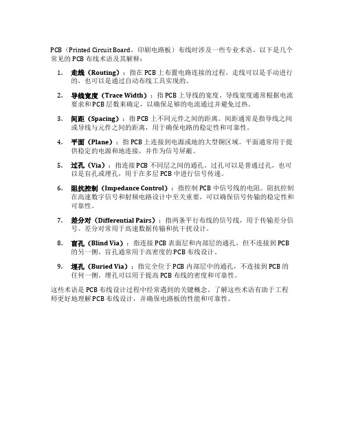
PCB(Printed Circuit Board,印刷电路板)布线时涉及一些专业术语。
以下是几个常见的 PCB 布线术语及其解释:1.走线(Routing):指在 PCB 上布置电路连接的过程。
走线可以是手动进行的,也可以是通过自动布线工具实现的。
2.导线宽度(Trace Width):指 PCB 上导线的宽度。
导线宽度通常根据电流要求和 PCB 层数来确定,以确保足够的电流通过并避免过热。
3.间距(Spacing):指 PCB 上不同元件之间的距离。
间距通常是指导线之间或导线与元件之间的距离,用于确保电路的稳定性和可靠性。
4.平面(Plane):指 PCB 上连接到电源或地的大型铜区域。
平面通常用于提供稳定的电源和地连接,并作为信号屏蔽。
5.过孔(Via):指连接 PCB 不同层之间的通孔。
过孔可以是普通过孔,也可以是盲孔或埋孔,用于在多层 PCB 中进行信号传递。
6.阻抗控制(Impedance Control):指控制 PCB 中信号线的电阻。
阻抗控制在高速数字信号和射频电路设计中至关重要,可以确保信号传输的稳定性和可靠性。
7.差分对(Differential Pairs):指两条平行布线的信号线,用于传输差分信号。
差分对常用于高速数据传输和抗干扰设计。
8.盲孔(Blind Via):指连接 PCB 表面层和内部层的通孔,但不连接到 PCB的另一侧。
盲孔通常用于高密度的 PCB 布线设计。
9.埋孔(Buried Via):指完全位于 PCB 内部层中的通孔,不连接到 PCB 的任何一侧。
埋孔可以用于提高 PCB 布线的密度和可靠性。
这些术语是 PCB 布线设计过程中经常遇到的关键概念。
了解这些术语有助于工程师更好地理解 PCB 布线设计,并确保电路板的性能和可靠性。
PCB术语——精选推荐
PCB术语PCB线路设计及制前作业术语1、Annular Ring 孔环指绕接通孔壁外平贴在板面上的铜环而言。
在内层板上此孔环常以十字桥与外面大地相连,且更常当成线路的端点或过站。
在外层板上除了当成线路的过站之外,也可当成零件脚插焊用的焊垫。
与此字同义的尚有 Pad(配圈)、 Land (独立点)等。
2、Artwork 底片在电路板工业中,此字常指的是黑白底片而言。
至于棕色的“偶氮片”(Diazo Film)则另用 Phototool 以名之。
PCB 所用的底片可分为“原始底片”Master Artwork 以及翻照后的“工作底片”Working Artwork 等。
3、Basic Grid 基本方格指电路板在设计时,其导体布局定位所着落的纵横格子。
早期的格距为 100 mil,目前由于细线密线的盛行,基本格距已再缩小到 50 mil。
4、Blind Via Hole 盲导孔指复杂的多层板中,部份导通孔因只需某几层之互连,故刻意不完全钻透,若其中有一孔口是连接在外层板的孔环上,这种如杯状死胡同的特殊孔,称之为“盲孔”(Blind Hole)。
5、Block Diagram 电路系统块图将组装板及所需的各种零组件,在设计图上以正方或长方形的空框加以框出,且用各种电性符号,对其各框的关系逐一联络,使组成有系统的架构图。
6、Bomb Sight 弹标原指轰炸机投弹的瞄准幕。
PCB 在底片制作时,为对准起见也在各角落设置这种上下两层对准用的靶标,其更精确之正式名称应叫做Photographers' Target。
7、Break-away panel 可断开板指许多面积较小的电路板,为了在下游装配线上的插件、放件、焊接等作业的方便起见,在 PCB 制程中,特将之并合在一个大板上,以进行各种加工。
完工时再以跳刀方式,在各独立小板之间进行局部切外形(Routing)断开,但却保留足够强度的数枚“连片”(Tie Bar 或Break-away Tab),且在连片与板边间再连钻几个小孔;或上下各切 V 形槽口,以利组装制程完毕后,还能将各板折断分开。
PCB术语
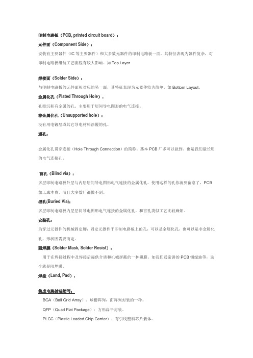
印制电路板(PCB, printed circuit board):元件面(Component Side):安装有主要器件(IC等主要器件)和大多数元器件的印制电路板一面,其特征表现为器件复杂,对印制电路板组装工艺流程有较大影响。
如Top Layer焊接面(Solder Side):与印制电路板的元件面相对应的另一面,其特征表现为元器件较为简单。
如Bottom Layout。
金属化孔(Plated Through Hole):孔壁沉积有金属的孔。
主要用于层间导电图形的电气连接。
非金属化孔(Unsupported hole):没有用电镀层或其它导电材料涂覆的孔。
通孔:金属化孔贯穿连接(Hole Through Connection)的简称。
基本PCB厂多可以做到。
也是我们最长用的电气连接孔。
盲孔(Blind via):多层印制电路板外层与内层层间导电图形电气连接的金属化孔。
使用这样的孔你就要留意了,PCB 加工成本贵,而且大多数厂都做不到。
埋孔(Buried Via):多层印制电路板内层层间导电图形电气连接的金属化孔。
和盲孔类似工艺比较麻烦。
安装孔:为穿过元器件的机械固定脚,固定元器件于印制电路板上的孔,可以是金属化孔,也可以是非金属化孔,形状因需要而定。
阻焊膜(Solder Mask, Solder Resist):用于在焊接过程中及焊接后提供介质和机械屏蔽的一种覆膜。
如我们通常讲的PCB铺绿油等,这个就是阻焊膜。
焊盘(Land, Pad):集成电路封装缩写:BGA(Ball Grid Array):球栅阵列,面阵列封装的一种。
QFP(Quad Flat Package):方形扁平封装。
PLCC(Plastic Leaded Chip Carrier):有引线塑料芯片栽体。
DIP(Dual In-line Package):双列直插封装。
SIP(Single inline Package):单列直插封装SOP(Small Out-Line Package):小外形封装。
PCB电路板术语
PCB Jargon (PCB专业术语) AAbsorption 吸收、吸入Accelerated Test(Aging)加速试验、加速老化Accelerator 加速剂、速化剂Accept/Acceptance 允收Acceptable Quality Level(AQL)允收品质水准Accuracy 准确度ACF:Adhesive copper foil 有胶铜箔Activator 活化剂、添加剂比称为ActivatorActive parts(Devices)主动零件,指积体电路或电晶体Addition Agent 添加剂Additive Process 加成法、分全加成、半加成及部份加成Adhesion 附著力Adhesive 胶类或接著剂Aging 老化Air Knife 风刀Ambient Temperature 环境温度Ampere 安培Amp-Hour 安培小时Annular Ring 孔环Anode 阳极Anode Bag 阳极带ANSI: American National Standard Institute 美国标准协会Anti-Forming Agent 消泡剂AOI: Automatic Optical Inspection 自动光学检验Aperture 开口APQP: Advanced Product Quality PlanArray 排列、阵列Artwork 底片ASIC: Application Specific Integrated Circuit 特定用途的积体电路器Aspect Ratio 纵横比、板厚与孔径之比值Assembly 装配、组装ATE: Automatic Testing Equipment 自动电测设备AVL: Approved Vender List 合格供应商BBack Light(Back Lighting)背光法Back-UP 垫板Backpanels/ Backplanes 背板、支持板,厚度较厚,Ball Grid Array(BGA)球脚车列(封装)Barrel 孔壁Base Material 基材Batch 批(同时间发料某一数量的板子)Bevelling 切斜边Binder 黏结剂Black oxide 黑氧化层,另有棕氧化(Brown Oxide)Blind Via Hole 盲导孔Blister 局部性分层或起泡Blockout 封网,网板之空网处以水溶胶涂满Blow Hole 吹孔,PTH孔壁有破洞(void)所造成Boiler (Water Tube Boiler/ Fire Tube Boiler)BOM: Bill of Material 用料表Bond Strength 结合强度Bonding Sheet(Layer) 接合片、接著层,指PP Bonding Wire 结合线,IC之晶片与PCB之引线Bow 板弯Break-away Panel 可断开板或者说Break Away Tab Break Point 出像点、影像点Break-Out 破出(钻孔破出开成断环情形)Bridging 搭桥、桥接Brightener 光泽剂Brush Plating 刷镀BTU/British Thermal Unit 英制热量单位Bump 突块Buried Via Hole 埋导孔Burn-in 高温加速老化试验Burning 烧焦Burr 毛头Buy-off 认可CCAD: Computer Aided Design 电脑辅助设计CAM: Computer Aided Manufacturing 电脑辅助制造CAT: Computer Aided Testing 电脑辅助测试Capacitance 电容Carbide 碳化物、碳化钨钻头CAR: Corrective Action Report 改善报告Carbon Treatment 活性碳处理Card 卡板Carrier 载体Cartridge 滤芯Cathode 阴极CCL: Copper Clad Laminates 铜箔基板Ceramics 陶瓷Certificate 证明书CFC 氟氯碳化物Chloro-Fluoro-CarbonChamfer 倒角、去掉直角Characteristic Impedance 特性阻抗Cheek list 检察清单Chip 晶粒、晶片Chip On Board 晶片黏著板Clean Room 无尘室(Class 100)Cleanliness 清洁度Clearance 余隙、余环COB(Chip on Board)晶片在板上直接组装COC(Certificate of Compliance)出货合格书COF(Chip on Flexible PCB)COG(Chip glass)Coefficient of Thermal Expansion 热膨胀系数(CTE)Cold Solder Joint 冷焊点Component Hole 零件孔Component Side 组件面、零件面Conditioning 整孔Conductivity 导电度Connector 连接器Continuity Test 连通性试验Copper Foil 铜箔、铜皮Copper Ball 铜球Corner Crack 镀通孔转角断角Cp: Capability of Process 制程能力指数Crack 裂痕Crazing 白斑(基板外观上的缺点)Crosstalk 杂讯、串讯Cure/Curing 硬化、热化Current Density (C.D.)电流密度(1 ASD=9.1 ASF)Curtain Coating 液涂法DDatum 基准点Deburring 去毛头Defect 不良缺点Degreasing 脱脂Delamination 分层、爆板Dent 凹陷、缓和均匀的下陷Desmearing 除胶渣Developer 显像液Deviation 偏差Device 电子元件Dewetting 缩锡DFM: Design for Manufacturing/Dirty foreign Materials 异物、杂质Die 冲模Dielectric 介质Dielectric Constant 介质常数Dimensional Stability 尺度安定性DIP(Dual Inline Package)双排脚封装体Direct Plating 直接电镀DI Water 纯水(De-Ionize Water)DOE/Design of Experiment 实验计划法DPPM(Defect Parts Per Million)Drilling 钻孔Drill Bit 钻针Dry Film 干膜Dummy 假镀EECN: Engineering Change Notice 工程变更通知Elongation 延伸性EMI 电磁干扰Electromagnetic InterferenceENIG: Electroless Nickel Immersion Gold 化镍浸金Entek 有机护铜处理Entry Material 盖板E.T/Electric Test 电测、电气测试Epoxy Resin 环氧树脂ESD: Electro-Static Discharge 静电流量Etching 蚀刻Etchback 加蚀Etch Factor 蚀刻函数Etching Resist 抗蚀阻剂Expose Copper 漏铜Exposure 曝光Eyelet 铆钉RivetFFAAR(First Article Approval Report)Failure 故障、损坏Fault 缺陷、瑕疵FCC/Federal Communication Commission 美国联邦通讯委员会Fiber Exposure 玻织显露Fiducial Mark 基准记号、光学点Film 底片Filter 过滤器Fine Line 细线Finger 手指Finishing 制成品在外观上的最后处理First Article 试产的首件或首批小量产品First Pass-Yield 初检良品率Fixture 夹具、治具(Rig and Fixture)Flame Resistant 耐燃性(分HB、VO、V1及V2等四级)Flux 助焊剂Foil Burr 铜箔毛边Foot Pint(Land Pattern)脚垫Foreign Material 外来物、异物FR4/Flame Resistant Laminates 耐燃性积层板材Frequency 频率GGauge 量规Gel Time 胶化时间Gerber Data/Gerber File 格搏档案Glass Fiber 玻璃纤维Glass Fiber Protrusion 玻纤突出Glass Transition Temperature/Tg 玻璃态转化温度Golden Board 测试用标准板Grid 标准格Ground Plane 接地层Guide Pin 导针HHaloing 白圈、白边(在钻孔、开槽等机械动作一旦过猛时将造成内部树脂之破碎或微小分层裂开的现象)Hardener 硬化剂Hardness 硬度Heat Dissipation 散热Hertz(Hz)赫芝HEPA/High Efficiency Particulate Air Filter 高效空气尘粒过滤机Hipot Test 高压电测High Potential Test Hit 擎Holding Time 停区时间Hole Block 孔塞Hole Breakout 孔位破出,简称BreakoutHole counter 数孔机Hole Density 孔数密度Hole Pull Strength 孔壁强度Hole Void 破洞Hot Air Levelling 喷锡HASL/HALTHE(High Temperature Elongation) 高温延伸性II.C.Socket 积体电路插座Image Transfer 影像转移IMC: Inter-metallic compound 介面合金共化物Immersion Plating 浸镀Impedance 阻抗In-Circuit Testing 组装板电测,ICTIndexing Hole 基准孔Infrared(IR) 红外线Ink 油墨Inner Layer 内层Input/Output 输入、输出Insert/Insertion 插接、插装Insulation Resistance 绝缘电阻Integrated Circuit (IC) 积体电路器Interconnection互连Intermatallic Compound(IMC) 介面合金共化物Internal Stress 内应力Ion Cleanliness 离子清洁度Ionic Contamination 离子污染IPC: The Institute for Interconnecting and Packaging Electronic Circuits 美国印刷电路板协会ISO: International Organization for Standardization 国际标准组织Isolation 隔离性JJPCA/Japan Print Circuit Association 日本印刷电路工业会Just-In-Time(JIT) 适时供应KKeyboard 键盘Kraft Paper 牛皮纸LLaminate(s) 基板、积层板Laminator 压膜机Land 孔环焊垫、独立点Landless Hole 无环通孔Laser Direct Imaging/LDI 雷射直接成像Laser Photoplotter 雷射曝光机、绘图机Lay Out 布线、布局(configuration, general arrangement)Lay Up 叠合Lead Frame 脚架Lead 引脚、接脚Legend 文字标记Levelling 整平Light Intensity 光强度LMW: License Manufacturing Warehouse 保税厂Lot Size 批量LRR(Lot Reject Rate)MMajor Defect 严重缺点、主要缺点Marking 标记Mask 阻剂Mass Lamination 大型压板MCM/Multi-Chip Module 多晶片模组Measling 白点Membrane Switch 薄膜开关Microctching 微蚀Microsectioning 微切片法Migration迁移Mil 英丝0.001 inmisregistration 对不准、对不准度MLB/Multi-Layer Board 多层板Modem 调变及解调器、数据机Modification 修改、改变Module 模组Mother Board 主机板NNail Head 钉头N.C.数值控制(Numerical Control)Negative 负片Negative etch-back 反回蚀Nick 缺口Node 节点Nodule 瘤Non-Conformance 不合格品Non-flammable 非燃性Non-wetting 不沾锡Normal Distribution 常态分配NPI:New project introduction)NRE Charge-Non-Recurring Engineering Charge 不会重收的工程费用OOhm 欧姆Omega Meter 离子污染检测仪Open Circuits 断线Optical Density 光密度Optical Inspection 光学检验Organic Solderability Preservatives(OSP) 有机保焊剂Outgassing 出气、吹气Output 产出、输出Overflow 溢流Oxidation氧化Ozone Depletion 臭氧层耗损PPackaging 封装、购装Packing 包装Pad 配圈、孔环焊垫Panel Plating 全板镀铜Passive Parts 被动零件,如电阻、电容Past 膏(锡膏Solder Paste)Pattern Plating 线路电镀PCB/Printed Circuit Board 印刷电路板Peel Strength 抗撕强度Peripheral 周边附属设备Phototool 底片(一般指偶氮棕片Diazo Film)Pin Grid Array(PGA) 矩阵式针脚封装Pinhole 针孔Pin 接脚、插梢、插针Pink Ring 粉红圈Pits 凹点(小面积下陷)Pitch 脚距、垫距、线距Plasma 电浆Plated through Hole/PTH 镀通孔Plug 插脚、塞孔Polarization 分极、极化Polyimide(PI) 聚亚酸胺Popcorn Effect 爆米花效应Post Cure 疏孔度试验Power Plane 后续硬化、后烤Power Supply 电源层PPM/Parts Per Million 百万分之几Preheat 预热Prepreg 胶片、树脂片Press Plate 压合钢板Press-Fit Contact 挤入式接触Printing 印刷Probe 探针Profile 轮廓、部面图、升温曲线图积线Punch 横切、冲床QQIT(Quality improvement Team) 品质改善小组Qualified Products List 合格产品(供应者)名单RRadiometer 辐射计、光度计Radius 尺角、半径Reference Dimension 参考尺度、参考尺寸Reflow Soldering 重熔焊接、熔焊Registration 对准度Reject 剔退、拒收Reliability 可靠度、信赖度Repair 修理Resin Content 胶含量、树脂含量Resin Flow 胶流量、树脂流量Resist 阻剂、阻膜Resistor 电阻器、电阻Resolution 解像、解像度、解析度Resolving Power 解析力、解像力(分辨力)Rework(ing) 重工、再加工Ring 套环Roller Cutter 混切机(俗称锯板机)Roller Coating 滚动涂布法Routing 切外型、捞外型RRM: Revolutions per Minute 转速(每分钟)Run-out 偏转、绕转、累积距差SSCAR(Supplier CA Request) 供应商改善报告SCM: Supply chain Management 供应商管理系统Scratch 刮痕Screen Printing 网版印刷Scrubber 磨刷机、磨刷器Selective Plating 选择性电镀SEM/Scanning Electron Microscope 扫瞄式电子显微镜Semi-Conductor 半导体Shearing 剪、裁切Short 短路Side Wall 侧壁Sigma(Standard Deviation) 标准差Signal 讯号Silicon 矽Silk Screen 网版印刷、丝网印刷Skin Effect 集肤效应Skip Printing 漏印Slot 槽孔Smear 胶渣SMT/Surface Mount Technology 表面黏装技术Solder 焊锡Solderability 焊锡性Solder Ball 锡球Solder Bridging 锡桥Solder Bump 焊锡凸块Solder Dam 锡堤(IC脚间的防焊)Solder Levelling 喷锡、热风整平Solder Mask(S/M) 绿漆、防焊膜Solder Paste 锡膏Solder Plug 锡塞、锡柱Solder Pot 锡炉Solder Side 焊锡面Soldering Fluid/Soldering Oil 助焊液、护焊汕Solid Content 固体含量SOP(Standard Operation Procedure) 标准作业程序Spacing 间距SPC/Statistical Process Control 统计制程管制Specific Gravity SG比重Specification(Spec) 规范、规格Specimen 样品、试样Spindle 钻轴Spray Coating 喷著涂装Stencil 版膜、网版Storage condition 储存条件Stress Relief 消除应力Substrate 底材Surface Tenting 表面张力Surface-Mount Device 表面黏装零件Swelling Agents/Sweller 膨胀剂SWR(Special Working Request) 试产前之“特殊工作要求”TTab 接点、金手指Tape 撕胶带试验Teflon 铁氟龙Temperature Profile 温度曲线Template 模板Tensile Strength 抗拉强度Tenting 盖孔法Terminal 端子Thermal Stress 热应力Thermal Shock 热冲击Thin Copper Foil 薄铜箔Then film Technology 薄膜技术Throwing Power 分布力Tolerance 公差Touch Up 检修(简单的工具在手操作下即可进行的小规范的检修,称之T ouch Up或Rewok 有些类似)Trace 线路、导线Traceability 追溯性、可溯性Transistor 电晶体Transmission Line 传输线Twist 板翘、板扭UUL 保险业试验Underwriters Laboratories/INCUltra Violet Curing(UV Curing) 紫外线硬化Ultrasonic Cleaning 超音波清洗Undercut/Undercutting 侧蚀Universal Tester 万用型电测机VVacuum Lamination 真空压合Vacuum Packing 真空包装Viscosity 黏滞度、黏度Vision Systems 视觉系统Visual Examination(Inspection) 目视检查Voltage 电压WWafer 晶圆Warp/Warpage 板弯Warp and Twist 板弯翘Washer 垫圈Waste Treatment 废弃处理Water Absorption 吸水性Water Break 水膜破散、水破Watermark 水印Wave Soldering 波焊Weave Exposure 织纹显露Weave Texture 织纹隐现Welding 熔接Wet Process 湿式制程Wetting Balance 沾锡、沾湿White Spot 白点Wicking effect 灯芯效应Wire Bonding 打线结合WIP(Working Piece in Process) 在制品XX Axis X轴X-Ray X光YY-Axis Y轴Yield 良品率、良率、产率ZZ-Axis X轴OtherHDI-High Density inter-connect 高密度内连接SWOT Strengths Weaknesses Opportunities ThreatsCD: Compact DiscCPU: Central Process UnitDLD: Direct Laser Drilling (CO2 Laser, YAG Laser)DVD: Digital Versatile DiscEEPROM: Electrically Erasable Programmable Read Only MemoryEMS: Electronics Manufacturing ServiceGPS: Global Positioning ServiceHDD: Hard Disk DriveHDTV: High Density TVLCD: Liquid Crystal DisplayLED: Light Emitting DiodeVCD: Video Compact DiskQuality System Requirements QS-9000(質量體系要求)Advanced Product Quality Planning and Control Plan APQP (產品質量先期策劃和控制計劃) Measurement Systems Analysis MSA(測量系統分析)Potential Failure Mode and Effects Analysis FMEA(潜在失效模式與後果分析)Production Part Approval Process PPAP (生產件批准程序)Statistical Process Control SPC (統計過程控制)IPC-A-600Classification 分级Acceptance Criteria 允收规格Applicable Documents 参考资料Dimensions And Tolerances 尺度与公差Terms And Definitions 术语及定义Workmanship 工艺水准Externally Observable Characteristics 外观特性Board Edges 板边Burrs 看头、毛刺Nonmetallic Burrs 非金属性毛头Metallic Burrs 金属毛头Nicks 缺口Haloing 白边Base Material 基材Weave Exposure 织纹显露Weave Texture 织纹隐现Exposed/Disrupted Fibers 玻织曝露/扰乱Pits and Voids 凹点与凹坑Base Material Subsurface 基材次表面Measling白点Crazing白斑Delamination/Blister分层/起泡Foreign Inclusions外来夹杂物Solder Coatings and Fused Tin Lead喷锡板或熔锡板Nonwetting拒锡(不沾锡)Dewetting缩锡Holes-Plated-Through-General镀通孔概要Nodules/Burrs镀瘤/毛头Pink Ring粉红圈Voids-Copper Plating镀铜层破洞Voids-Finished Coating完工皮膜之镀层破洞Lifted Lands-(Visual)孔环浮离(目检)Holes-Unsupported未镀孔Haloing白圈Printed Contacts板边接触金手指Surface Plating-General表面镀层通则Surface Plating-Wire Bond Pads打线承垫之表面Burrs on Edge-Board Contacts板边接点之毛头Adhesion of Overplate表面镀层之附着力Marking标记Etched Marking蚀刻标记Screened or Ink Stamped Marking纲印或盖印之标记Solder Resist(Solder Mask)防焊绿漆Coverage Over Conductors (Skip Coverage) 边线表面之覆盖性(覆盖不全、跳印)Registration to Holes (All Finishes) 对孔之套准度(各种表处理层)Registration to Other Conductive Patterns 其他防焊的对准性Ball Grid Array (Solder Resist-Defined Lands) 球脚格列体之焊垫(绿漆设限之焊垫)Ball Grid Array (Copper-Defined Lands) 球脚格列体(铜面设限之焊垫)Ball Grid Array (Solder Dam) 球脚格列体(防焊堤)Blisters/Delamination起泡/分层Adhesion(Flaking or Peeling)附著力(破片或剥落)Waves/Wrinkles/Ripples起浪/起皱/纹路Tenting(Via Holes)盖孔(导通孔、过孔)Pattern Definition-Dimensional圆形尺度特性Conductor Width and Spacing线宽与间距Conductor Width线宽Conductor Spacing导线间距External Annular Ring-Measurement孔环测量External Annular Ring-Supported Holes有孔壁支援的外孔环External Annular Ring-Unsupported Holes无孔壁支援的外孔环Flatness平坦度Internally Observable Characteristics可观察到的内在特性Dielectric Materials介质材料Laminate Voids(Outside Thermal Zone)压板空洞(或热区之外)Registration/Conductors to Holes导体与通孔之间的对准度Clearance Hole/Unsupported/to Power/Ground Planes 针对电源层或接地层具隔环之非镀通孔Delamination/Blister分层/起泡Etchback回蚀Negative Etchback反回蚀Smear Removal除胶渣Dielectric Material/Clearance/Metal Plane for Supported Holes 金属层与通孔壁之介质隔距Layer-to-Layer Spacing层与层之间距Resin Recession树脂缩陷Conductive Patterns-General导线概论Etching Characteristics蚀刻特性Print and Etch印后即蚀刻(指正片法)Surface Conductor Thickness(Foil Plus Plating)表导体厚度(铜箔加电镀铜)Foil Thickness-Internal Layers内层箔厚Plated-Through Holes-General镀通孔概论Annular Ring-Internal Layers各内层之孔环Lifted Lands-(Cross-Sections)焊环浮起(切片上所见)Foil Crack-(Internal Foil)“C”Crack内层铜箔之裂纹Foil Crack-(External Foil)镀层破裂Plating Crack-(Barrel)“E”Crack孔壁镀层破裂Plating Crack-(Corner)“F”Crack孔角镀层破裂Plating Nodules镀层长瘤Copper Plating Thickness-Hole Wall孔壁镀铜厚度Plating Voids镀层破洞Solder Coating Thickness (Only When Specified) 焊锡皮膜厚度(当已规定检查者)Solder Resist Thickness绿漆厚度Wicking灯芯效应(指玻织束渗入化学铜)Wicking/Clearance Holes隔离孔之渗铜Innerlayer Separation-Vertical (Axial) Microsection 内层(环)分离-垂直(纵断面)微切片Innerlayer Separation-Horizontal (Transverse) Microsection 内层(环)分离-水平(横断面)微切片Material Fill of Blind and Buried Vias盲孔与埋孔之填充材料钻孔式镀通孔Plated-Through Holes-Drilled钻孔式镀通孔Burrs毛头Nailheading钉头Plated-Through Holes-Punched冲孔式镀通孔Roughness and Nodules粗糙与镀瘤Flare喇叭口Miscellaneous其他离顶Flexible And Rigid-Flex Printed Wiring软性及软硬合板Metal Core Printed Boards金属平心电路板Type Classifications型式分类Spacing Laminated Type间距压合板Insulation Thickness/Insulated Metal Substrate已绝缘金属底材之绝缘厚度Insulation Material Fill/Laminated Type Metal Core压合型金属平心之绝缘填料Cracks in Insulation Material Fill/Laminated Type压合型绝缘填充料之裂纹Core Bond to Plated-Through Hole Wall平心层与镀通孔之间的固著Flush Printed Boards表面全平板Flushness of Surface Conductor表面导线之平坦性Cleanliness Testing清洁度试验Solderability Testing焊锡性试验Plated-Through Holes镀通孔Electrical Integrity电性之完整平行光曝光机:Collimated ExposureCollimated Exposure二次元测量仪two dimension measuring instrument,镀层厚度测试仪Plating Thickness Tester电导率测试仪:Conductometer剥离强度测试仪peel strength TesterROHS检测仪ROHS TesterLCR测试仪LCR Tester喷砂机:sandblasting machine磨板机:Scrubbing立式圆角机Corner rounding Machine开短路测试机short circuit tester碱性蚀刻机:alkalineetchingmachine剪板机: steel plate shearer高温烤箱high-temperature oven飞针测试机:Flying Probe E-Test Machine铣边机edge milling machine超声波清洗机ultrasonic cleanersDES水平线DES level自私,让我们只看见自己却容不下别人。
PCB电路板术语

PCB Jargon (PCB专业术语) AAbsorption 吸收、吸入Accelerated Test(Aging)加速试验、加速老化Accelerator 加速剂、速化剂Accept/Acceptance 允收Acceptable Quality Level(AQL)允收品质水准Accuracy 准确度ACF:Adhesive copper foil 有胶铜箔Activator 活化剂、添加剂比称为ActivatorActive parts(Devices)主动零件,指积体电路或电晶体Addition Agent 添加剂Additive Process 加成法、分全加成、半加成及部份加成Adhesion 附著力Adhesive 胶类或接著剂Aging 老化Air Knife 风刀Ambient Temperature 环境温度Ampere 安培Amp-Hour 安培小时Annular Ring 孔环Anode 阳极Anode Bag 阳极带ANSI: American National Standard Institute 美国标准协会Anti-Forming Agent 消泡剂AOI: Automatic Optical Inspection 自动光学检验Aperture 开口APQP: Advanced Product Quality PlanArray 排列、阵列Artwork 底片ASIC: Application Specific Integrated Circuit 特定用途的积体电路器Aspect Ratio 纵横比、板厚与孔径之比值Assembly 装配、组装ATE: Automatic Testing Equipment 自动电测设备AVL: Approved Vender List 合格供应商BBack Light(Back Lighting)背光法Back-UP 垫板Backpanels/ Backplanes 背板、支持板,厚度较厚,Ball Grid Array(BGA)球脚车列(封装)Barrel 孔壁Base Material 基材Batch 批(同时间发料某一数量的板子)Bevelling 切斜边Binder 黏结剂Black oxide 黑氧化层,另有棕氧化(Brown Oxide)Blind Via Hole 盲导孔Blister 局部性分层或起泡Blockout 封网,网板之空网处以水溶胶涂满Blow Hole 吹孔,PTH孔壁有破洞(void)所造成Boiler (Water Tube Boiler/ Fire Tube Boiler)BOM: Bill of Material 用料表Bond Strength 结合强度Bonding Sheet(Layer) 接合片、接著层,指PP Bonding Wire 结合线,IC之晶片与PCB之引线Bow 板弯Break-away Panel 可断开板或者说Break Away Tab Break Point 出像点、影像点Break-Out 破出(钻孔破出开成断环情形)Bridging 搭桥、桥接Brightener 光泽剂Brush Plating 刷镀BTU/British Thermal Unit 英制热量单位Bump 突块Buried Via Hole 埋导孔Burn-in 高温加速老化试验Burning 烧焦Burr 毛头Buy-off 认可CCAD: Computer Aided Design 电脑辅助设计CAM: Computer Aided Manufacturing 电脑辅助制造CAT: Computer Aided Testing 电脑辅助测试Capacitance 电容Carbide 碳化物、碳化钨钻头CAR: Corrective Action Report 改善报告Carbon Treatment 活性碳处理Card 卡板Carrier 载体Cartridge 滤芯Cathode 阴极CCL: Copper Clad Laminates 铜箔基板Ceramics 陶瓷Certificate 证明书CFC 氟氯碳化物Chloro-Fluoro-CarbonChamfer 倒角、去掉直角Characteristic Impedance 特性阻抗Cheek list 检察清单Chip 晶粒、晶片Chip On Board 晶片黏著板Clean Room 无尘室(Class 100)Cleanliness 清洁度Clearance 余隙、余环COB(Chip on Board)晶片在板上直接组装COC(Certificate of Compliance)出货合格书COF(Chip on Flexible PCB)COG(Chip glass)Coefficient of Thermal Expansion 热膨胀系数(CTE)Cold Solder Joint 冷焊点Component Hole 零件孔Component Side 组件面、零件面Conditioning 整孔Conductivity 导电度Connector 连接器Continuity Test 连通性试验Copper Foil 铜箔、铜皮Copper Ball 铜球Corner Crack 镀通孔转角断角Cp: Capability of Process 制程能力指数Crack 裂痕Crazing 白斑(基板外观上的缺点)Crosstalk 杂讯、串讯Cure/Curing 硬化、热化Current Density (C.D.)电流密度(1 ASD=9.1 ASF)Curtain Coating 液涂法DDatum 基准点Deburring 去毛头Defect 不良缺点Degreasing 脱脂Delamination 分层、爆板Dent 凹陷、缓和均匀的下陷Desmearing 除胶渣Developer 显像液Deviation 偏差Device 电子元件Dewetting 缩锡DFM: Design for Manufacturing/Dirty foreign Materials 异物、杂质Die 冲模Dielectric 介质Dielectric Constant 介质常数Dimensional Stability 尺度安定性DIP(Dual Inline Package)双排脚封装体Direct Plating 直接电镀DI Water 纯水(De-Ionize Water)DOE/Design of Experiment 实验计划法DPPM(Defect Parts Per Million)Drilling 钻孔Drill Bit 钻针Dry Film 干膜Dummy 假镀EECN: Engineering Change Notice 工程变更通知Elongation 延伸性EMI 电磁干扰Electromagnetic InterferenceENIG: Electroless Nickel Immersion Gold 化镍浸金Entek 有机护铜处理Entry Material 盖板E.T/Electric Test 电测、电气测试Epoxy Resin 环氧树脂ESD: Electro-Static Discharge 静电流量Etching 蚀刻Etchback 加蚀Etch Factor 蚀刻函数Etching Resist 抗蚀阻剂Expose Copper 漏铜Exposure 曝光Eyelet 铆钉RivetFFAAR(First Article Approval Report)Failure 故障、损坏Fault 缺陷、瑕疵FCC/Federal Communication Commission 美国联邦通讯委员会Fiber Exposure 玻织显露Fiducial Mark 基准记号、光学点Film 底片Filter 过滤器Fine Line 细线Finger 手指Finishing 制成品在外观上的最后处理First Article 试产的首件或首批小量产品First Pass-Yield 初检良品率Fixture 夹具、治具(Rig and Fixture)Flame Resistant 耐燃性(分HB、VO、V1及V2等四级)Flux 助焊剂Foil Burr 铜箔毛边Foot Pint(Land Pattern)脚垫Foreign Material 外来物、异物FR4/Flame Resistant Laminates 耐燃性积层板材Frequency 频率GGauge 量规Gel Time 胶化时间Gerber Data/Gerber File 格搏档案Glass Fiber 玻璃纤维Glass Fiber Protrusion 玻纤突出Glass Transition Temperature/Tg 玻璃态转化温度Golden Board 测试用标准板Grid 标准格Ground Plane 接地层Guide Pin 导针HHaloing 白圈、白边(在钻孔、开槽等机械动作一旦过猛时将造成内部树脂之破碎或微小分层裂开的现象)Hardener 硬化剂Hardness 硬度Heat Dissipation 散热Hertz(Hz)赫芝HEPA/High Efficiency Particulate Air Filter 高效空气尘粒过滤机Hipot Test 高压电测High Potential Test Hit 擎Holding Time 停区时间Hole Block 孔塞Hole Breakout 孔位破出,简称BreakoutHole counter 数孔机Hole Density 孔数密度Hole Pull Strength 孔壁强度Hole Void 破洞Hot Air Levelling 喷锡HASL/HALTHE(High Temperature Elongation) 高温延伸性II.C.Socket 积体电路插座Image Transfer 影像转移IMC: Inter-metallic compound 介面合金共化物Immersion Plating 浸镀Impedance 阻抗In-Circuit Testing 组装板电测,ICTIndexing Hole 基准孔Infrared(IR) 红外线Ink 油墨Inner Layer 内层Input/Output 输入、输出Insert/Insertion 插接、插装Insulation Resistance 绝缘电阻Integrated Circuit (IC) 积体电路器Interconnection互连Intermatallic Compound(IMC) 介面合金共化物Internal Stress 内应力Ion Cleanliness 离子清洁度Ionic Contamination 离子污染IPC: The Institute for Interconnecting and Packaging Electronic Circuits 美国印刷电路板协会ISO: International Organization for Standardization 国际标准组织Isolation 隔离性JJPCA/Japan Print Circuit Association 日本印刷电路工业会Just-In-Time(JIT) 适时供应Keyboard 键盘Kraft Paper 牛皮纸LLaminate(s) 基板、积层板Laminator 压膜机Land 孔环焊垫、独立点Landless Hole 无环通孔Laser Direct Imaging/LDI 雷射直接成像Laser Photoplotter 雷射曝光机、绘图机Lay Out 布线、布局(configuration, general arrangement) Lay Up 叠合Lead Frame 脚架Lead 引脚、接脚Legend 文字标记Levelling 整平Light Intensity 光强度LMW: License Manufacturing Warehouse 保税厂Lot Size 批量LRR(Lot Reject Rate)MMajor Defect 严重缺点、主要缺点Marking 标记Mask 阻剂Mass Lamination 大型压板MCM/Multi-Chip Module 多晶片模组Measling 白点Membrane Switch 薄膜开关Microctching 微蚀Microsectioning 微切片法Migration迁移Mil 英丝0.001 inmisregistration 对不准、对不准度MLB/Multi-Layer Board 多层板Modem 调变及解调器、数据机Modification 修改、改变Module 模组Mother Board 主机板Nail Head 钉头N.C.数值控制(Numerical Control)Negative 负片Negative etch-back 反回蚀Nick 缺口Node 节点Nodule 瘤Non-Conformance 不合格品Non-flammable 非燃性Non-wetting 不沾锡Normal Distribution 常态分配NPI:New project introduction)NRE Charge-Non-Recurring Engineering Charge 不会重收的工程费用OOhm 欧姆Omega Meter 离子污染检测仪Open Circuits 断线Optical Density 光密度Optical Inspection 光学检验Organic Solderability Preservatives(OSP) 有机保焊剂Outgassing 出气、吹气Output 产出、输出Overflow 溢流Oxidation氧化Ozone Depletion 臭氧层耗损PPackaging 封装、购装Packing 包装Pad 配圈、孔环焊垫Panel Plating 全板镀铜Passive Parts 被动零件,如电阻、电容Past 膏(锡膏Solder Paste)Pattern Plating 线路电镀PCB/Printed Circuit Board 印刷电路板Peel Strength 抗撕强度Peripheral 周边附属设备Phototool 底片(一般指偶氮棕片Diazo Film)Pin Grid Array(PGA) 矩阵式针脚封装Pinhole 针孔Pin 接脚、插梢、插针Pink Ring 粉红圈Pits 凹点(小面积下陷)Pitch 脚距、垫距、线距Plasma 电浆Plated through Hole/PTH 镀通孔Plug 插脚、塞孔Polarization 分极、极化Polyimide(PI) 聚亚酸胺Popcorn Effect 爆米花效应Post Cure 疏孔度试验Power Plane 后续硬化、后烤Power Supply 电源层PPM/Parts Per Million 百万分之几Preheat 预热Prepreg 胶片、树脂片Press Plate 压合钢板Press-Fit Contact 挤入式接触Printing 印刷Probe 探针Profile 轮廓、部面图、升温曲线图积线Punch 横切、冲床QQIT(Quality improvement Team) 品质改善小组Qualified Products List 合格产品(供应者)名单RRadiometer 辐射计、光度计Radius 尺角、半径Reference Dimension 参考尺度、参考尺寸Reflow Soldering 重熔焊接、熔焊Registration 对准度Reject 剔退、拒收Reliability 可靠度、信赖度Repair 修理Resin Content 胶含量、树脂含量Resin Flow 胶流量、树脂流量Resist 阻剂、阻膜Resistor 电阻器、电阻Resolution 解像、解像度、解析度Resolving Power 解析力、解像力(分辨力)Rework(ing) 重工、再加工Ring 套环Roller Cutter 混切机(俗称锯板机)Roller Coating 滚动涂布法Routing 切外型、捞外型RRM: Revolutions per Minute 转速(每分钟)Run-out 偏转、绕转、累积距差SSCAR(Supplier CA Request) 供应商改善报告SCM: Supply chain Management 供应商管理系统Scratch 刮痕Screen Printing 网版印刷Scrubber 磨刷机、磨刷器Selective Plating 选择性电镀SEM/Scanning Electron Microscope 扫瞄式电子显微镜Semi-Conductor 半导体Shearing 剪、裁切Short 短路SIR(Surface Insulation Resistance) 表面绝缘电阻Side Wall 侧壁Sigma(Standard Deviation) 标准差Signal 讯号Silicon 矽Silk Screen 网版印刷、丝网印刷Skin Effect 集肤效应Skip Printing 漏印Slot 槽孔Smear 胶渣SMT/Surface Mount Technology 表面黏装技术Solder 焊锡Solderability 焊锡性Solder Ball 锡球Solder Bridging 锡桥Solder Bump 焊锡凸块Solder Dam 锡堤(IC脚间的防焊)Solder Levelling 喷锡、热风整平Solder Mask(S/M) 绿漆、防焊膜Solder Paste 锡膏Solder Plug 锡塞、锡柱Solder Pot 锡炉Solder Side 焊锡面Soldering Fluid/Soldering Oil 助焊液、护焊汕Solid Content 固体含量SOP(Standard Operation Procedure) 标准作业程序Spacing 间距SPC/Statistical Process Control 统计制程管制Specific Gravity SG比重Specification(Spec) 规范、规格Specimen 样品、试样Spindle 钻轴Spray Coating 喷著涂装Stencil 版膜、网版Storage condition 储存条件Stress Relief 消除应力Substrate 底材Surface Insulation Resistance(SIR) 表面绝缘电阻Surface Tenting 表面张力Surface-Mount Device 表面黏装零件Swelling Agents/Sweller 膨胀剂SWR(Special Working Request) 试产前之“特殊工作要求”TTab 接点、金手指Tape 撕胶带试验Teflon 铁氟龙Temperature Profile 温度曲线Template 模板Tensile Strength 抗拉强度Tenting 盖孔法Terminal 端子Thermal Stress 热应力Thermal Shock 热冲击Thin Copper Foil 薄铜箔Then film Technology 薄膜技术Throwing Power 分布力Tolerance 公差Touch Up 检修(简单的工具在手操作下即可进行的小规范的检修,称之T ouch Up或Rewok 有些类似)Trace 线路、导线Traceability 追溯性、可溯性Transistor 电晶体Transmission Line 传输线Twist 板翘、板扭UUL 保险业试验Underwriters Laboratories/INC Ultra Violet Curing(UV Curing) 紫外线硬化Ultrasonic Cleaning 超音波清洗Undercut/Undercutting 侧蚀Universal Tester 万用型电测机VVacuum Lamination 真空压合Vacuum Packing 真空包装Viscosity 黏滞度、黏度Vision Systems 视觉系统Visual Examination(Inspection) 目视检查Voltage 电压WWafer 晶圆Warp/Warpage 板弯Warp and Twist 板弯翘Washer 垫圈Waste Treatment 废弃处理Water Absorption 吸水性Water Break 水膜破散、水破Watermark 水印Wave Soldering 波焊Weave Exposure 织纹显露Weave Texture 织纹隐现Welding 熔接Wet Process 湿式制程Wetting Balance 沾锡、沾湿White Spot 白点Wicking effect 灯芯效应Wire Bonding 打线结合WIP(Working Piece in Process) 在制品XX Axis X轴X-Ray X光YY-Axis Y轴Yield 良品率、良率、产率ZZ-Axis X轴OtherHDI-High Density inter-connect 高密度内连接SWOT Strengths Weaknesses Opportunities ThreatsCD: Compact DiscCPU: Central Process UnitDLD: Direct Laser Drilling (CO2 Laser, YAG Laser)DVD: Digital Versatile DiscEEPROM: Electrically Erasable Programmable Read Only MemoryEMS: Electronics Manufacturing ServiceGPS: Global Positioning ServiceHDD: Hard Disk DriveHDTV: High Density TVLCD: Liquid Crystal DisplayLED: Light Emitting DiodeVCD: Video Compact DiskQuality System Requirements QS-9000(質量體系要求)Advanced Product Quality Planning and Control Plan APQP (產品質量先期策劃和控制計劃) Measurement Systems Analysis MSA(測量系統分析)Potential Failure Mode and Effects Analysis FMEA(潜在失效模式與後果分析)Production Part Approval Process PPAP (生產件批准程序)Statistical Process Control SPC (統計過程控制)IPC-A-600Classification 分级Acceptance Criteria 允收规格Applicable Documents 参考资料Dimensions And Tolerances 尺度与公差Terms And Definitions 术语及定义Workmanship 工艺水准Externally Observable Characteristics 外观特性Board Edges 板边Burrs 看头、毛刺Nonmetallic Burrs 非金属性毛头Metallic Burrs 金属毛头Nicks 缺口Haloing 白边Base Material 基材Weave Exposure 织纹显露Weave Texture 织纹隐现Exposed/Disrupted Fibers 玻织曝露/扰乱Pits and Voids 凹点与凹坑Base Material Subsurface 基材次表面Measling白点Crazing白斑Delamination/Blister分层/起泡Foreign Inclusions外来夹杂物Solder Coatings and Fused Tin Lead喷锡板或熔锡板Nonwetting拒锡(不沾锡)Dewetting缩锡Holes-Plated-Through-General镀通孔概要Nodules/Burrs镀瘤/毛头Pink Ring粉红圈Voids-Copper Plating镀铜层破洞Voids-Finished Coating完工皮膜之镀层破洞Lifted Lands-(Visual)孔环浮离(目检)Holes-Unsupported未镀孔Haloing白圈Printed Contacts板边接触金手指Surface Plating-General表面镀层通则Surface Plating-Wire Bond Pads打线承垫之表面Burrs on Edge-Board Contacts板边接点之毛头Adhesion of Overplate表面镀层之附着力Marking标记Etched Marking蚀刻标记Screened or Ink Stamped Marking纲印或盖印之标记Solder Resist(Solder Mask)防焊绿漆Coverage Over Conductors (Skip Coverage) 边线表面之覆盖性(覆盖不全、跳印)Registration to Holes (All Finishes) 对孔之套准度(各种表处理层)Registration to Other Conductive Patterns 其他防焊的对准性Ball Grid Array (Solder Resist-Defined Lands) 球脚格列体之焊垫(绿漆设限之焊垫)Ball Grid Array (Copper-Defined Lands) 球脚格列体(铜面设限之焊垫)Ball Grid Array (Solder Dam) 球脚格列体(防焊堤)Blisters/Delamination起泡/分层Adhesion(Flaking or Peeling)附著力(破片或剥落)Waves/Wrinkles/Ripples起浪/起皱/纹路Tenting(Via Holes)盖孔(导通孔、过孔)Pattern Definition-Dimensional圆形尺度特性Conductor Width and Spacing线宽与间距Conductor Width线宽Conductor Spacing导线间距External Annular Ring-Measurement孔环测量External Annular Ring-Supported Holes有孔壁支援的外孔环External Annular Ring-Unsupported Holes无孔壁支援的外孔环Flatness平坦度Internally Observable Characteristics可观察到的内在特性Dielectric Materials介质材料Laminate Voids(Outside Thermal Zone)压板空洞(或热区之外)Registration/Conductors to Holes导体与通孔之间的对准度Clearance Hole/Unsupported/to Power/Ground Planes 针对电源层或接地层具隔环之非镀通孔Delamination/Blister分层/起泡Etchback回蚀Negative Etchback反回蚀Smear Removal除胶渣Dielectric Material/Clearance/Metal Plane for Supported Holes 金属层与通孔壁之介质隔距Layer-to-Layer Spacing层与层之间距Resin Recession树脂缩陷Conductive Patterns-General导线概论Etching Characteristics蚀刻特性Print and Etch印后即蚀刻(指正片法)Surface Conductor Thickness(Foil Plus Plating)表导体厚度(铜箔加电镀铜)Foil Thickness-Internal Layers内层箔厚Plated-Through Holes-General镀通孔概论Annular Ring-Internal Layers各内层之孔环Lifted Lands-(Cross-Sections)焊环浮起(切片上所见)Foil Crack-(Internal Foil)“C”Crack内层铜箔之裂纹Foil Crack-(External Foil)镀层破裂Plating Crack-(Barrel)“E”Cra ck孔壁镀层破裂Plating Crack-(Corner)“F”Crack孔角镀层破裂Plating Nodules镀层长瘤Copper Plating Thickness-Hole Wall孔壁镀铜厚度Plating Voids镀层破洞Solder Coating Thickness (Only When Specified) 焊锡皮膜厚度(当已规定检查者)Solder Resist Thickness绿漆厚度Wicking灯芯效应(指玻织束渗入化学铜)Wicking/Clearance Holes隔离孔之渗铜Innerlayer Separation-Vertical (Axial) Microsection 内层(环)分离-垂直(纵断面)微切片Innerlayer Separation-Horizontal (Transverse) Microsection 内层(环)分离-水平(横断面)微切片Material Fill of Blind and Buried Vias盲孔与埋孔之填充材料钻孔式镀通孔Plated-Through Holes-Drilled钻孔式镀通孔Burrs毛头Nailheading钉头Plated-Through Holes-Punched冲孔式镀通孔Roughness and Nodules粗糙与镀瘤Flare喇叭口Miscellaneous其他离顶Flexible And Rigid-Flex Printed Wiring软性及软硬合板Metal Core Printed Boards金属平心电路板Type Classifications型式分类Spacing Laminated Type间距压合板Insulation Thickness/Insulated Metal Substrate已绝缘金属底材之绝缘厚度Insulation Material Fill/Laminated Type Metal Core压合型金属平心之绝缘填料Cracks in Insulation Material Fill/Laminated Type压合型绝缘填充料之裂纹Core Bond to Plated-Through Hole Wall平心层与镀通孔之间的固著Flush Printed Boards表面全平板Flushness of Surface Conductor表面导线之平坦性Cleanliness Testing清洁度试验Solderability Testing焊锡性试验Plated-Through Holes镀通孔Electrical Integrity电性之完整平行光曝光机:Collimated ExposureCollimated Exposure二次元测量仪two dimension measuring instrument,镀层厚度测试仪Plating Thickness Tester电导率测试仪:Conductometer剥离强度测试仪peel strength TesterROHS检测仪ROHS TesterLCR测试仪LCR Tester喷砂机:sandblasting machine磨板机:Scrubbing立式圆角机Corner rounding Machine开短路测试机short circuit tester碱性蚀刻机:alkalineetchingmachine剪板机: steel plate shearer高温烤箱high-temperature oven飞针测试机:Flying Probe E-Test Machine铣边机edge milling machine超声波清洗机ultrasonic cleanersDES水平线DES level自私,让我们只看见自己却容不下别人。
pcb常用的专业术语
pcb常用的专业术语PCB(Printed Circuit Board,印刷电路板)是现代电子产品中不可或缺的组成部分。
作为电子元器件的载体,PCB承载着电子元器件的布局和连接,实现了电路的功能。
在PCB设计和制造过程中,涉及到许多专业术语和概念。
接下来,让我们逐一介绍一些常用的PCB专业术语。
1. 贴片技术(SMT,Surface Mount Technology):贴片技术是一种将表面贴装元件(Surface Mount Device,SMD)焊接至PCB上的技术。
相比传统的插件技术,贴片技术具有体积小、重量轻、可以实现自动化生产等优点。
2. 过孔(Via):过孔是连接PCB不同层的通孔,用于导电和信号传输。
根据其结构,可分为普通过孔和盲孔、埋孔。
3. 大地层(GND Plane):大地层是PCB中用于连接地电位的铜层或导电层。
大地层可以提供可靠的电气连接和较低的电阻,以降低电磁干扰和杂散信号。
4. 线路宽度(Trace Width):线路宽度是指PCB上导线的宽度。
其大小直接影响着导线的电流承载能力和电阻值。
通常,线路宽度越宽,其电流承载能力越大。
5. 线距(Trace Spacing):线距是指PCB上两个导线之间的间距。
线距的大小对于防止导线之间的电气干扰和放电有重要作用。
6. 丝印(Silk Screen):丝印是印刷在PCB表面的文字和图形标记。
它可以用于标注元件的位置、极性、参考设计ator等信息,以及产品品牌或商标。
7. 阻焊(Solder Mask):阻焊是一层覆盖在PCB焊盘和丝印之上的保护层。
它可以防止焊接过程中的短路和氧化,提高焊接质量和可靠性。
8. 电气孔(Test Pad):电气孔用于进行PCB电气测试,以验证电路的正确性和可靠性。
电气孔通常位于PCB的边缘,方便测试针对测试。
9. 焊盘(Pad):焊盘是用于连接和固定元件引脚的金属区域。
焊盘通过焊锡与元件引脚焊接在一起,实现电气和力学连接。
PCB电子线路板专业术语
PCB电子线路板专业术语一、综合词汇1、印制电路:printed circuit2、印制线路:printed wiring3、印制板:printed board4、印制板电路:printed circuit board (PCB)5、印制线路板:printed wiring board(PWB)6、印制元件:printed component7、印制接点:printed contact8、印制板装配:printed board assembly9、板:board10、单面印制板:single-sided printed board(SSB)11、双面印制板:double-sided printed board(DSB)12、多层印制板:mulitlayer printed board(MLB)13、多层印制电路板:mulitlayer printed circuit board14、多层印制线路板:mulitlayer prited wiring board15、刚性印制板:rigid printed board16、刚性单面印制板:rigid single-sided printed borad17、刚性双面印制板:rigid double-sided printed borad18、刚性多层印制板:rigid multilayer printed board19、挠性多层印制板:flexible multilayer printed board20、挠性印制板:flexible printed board21、挠性单面印制板:flexible single-sided printed board22、挠性双面印制板:flexible double-sided printed board23、挠性印制电路:flexible printed circuit (FPC)24、挠性印制线路:flexible printed wiring25、刚性印制板:flex-rigid printed board, rigid-flex printed board26、刚性双面印制板:flex-rigid double-sided printed board, rigid-flex double-sided printed27、刚性多层印制板:flex-rigid multilayer printed board, rigid-flex multilayer printed board28、齐平印制板:flush printed board29、金属芯印制板:metal core printed board30、金属基印制板:metal base printed board31、多重布线印制板:mulit-wiring printed board32、陶瓷印制板:ceramic substrate printed board33、导电胶印制板:electroconductive paste printed board34、模塑电路板:molded circuit board35、模压印制板:stamped printed wiring board36、顺序层压多层印制板:sequentially-laminated mulitlayer37、散线印制板:discrete wiring board38、微线印制板:micro wire board39、积层印制板:buile-up printed board40、积层多层印制板:build-up mulitlayer printed board (BUM)41、积层挠印制板:build-up flexible printed board42、表面层合电路板:surface laminar circuit (SLC)43、埋入凸块连印制板:B2it printed board44、多层膜基板:multi-layered film substrate(MFS)45、层间全内导通多层印制板:ALIVH multilayer printed board46、载芯片板:chip on board (COB)47、埋电阻板:buried resistance board48、母板:mother board49、子板:daughter board50、背板:backplane51、裸板:bare board52、键盘板夹心板:copper-invar-copper board53、动态挠性板:dynamic flex board54、静态挠性板:static flex board55、可断拼板:break-away planel56、电缆:cable57、挠性扁平电缆:flexible flat cable (FFC)58、薄膜开关:membrane switch59、混合电路:hybrid circuit60、厚膜:thick film61、厚膜电路:thick film circuit62、薄膜:thin film63、薄膜混合电路:thin film hybrid circuit64、互连:interconnection65、导线:conductor trace line66、齐平导线:flush conductor67、传输线:transmission line68、跨交:crossover69、板边插头:edge-board contact70、增强板:stiffener71、基底:substrate72、基板面:real estate73、导线面:conductor side74、元件面:component side75、焊接面:solder side76、印制:printing77、网格:grid78、图形:pattern79、导电图形:conductive pattern80、非导电图形:non-conductive pattern81、字符:legend82、标志:mark二、基材:1、基材:base material2、层压板:laminate3、覆金属箔基材:metal-clad bade material4、覆铜箔层压板:copper-clad laminate (CCL)5、单面覆铜箔层压板:single-sided copper-clad laminate6、双面覆铜箔层压板:double-sided copper-clad laminate7、复合层压板:composite laminate8、薄层压板:thin laminate9、金属芯覆铜箔层压板:metal core copper-clad laminate10、金属基覆铜层压板:metal base copper-clad laminate11、挠性覆铜箔绝缘薄膜:flexible copper-clad dielectric film12、基体材料:basis material13、预浸材料:prepreg14、粘结片:bonding sheet15、预浸粘结片:preimpregnated bonding sheer16、环氧玻璃基板:epoxy glass substrate17、加成法用层压板:laminate for additive process18、预制内层覆箔板:mass lamination panel19、内层芯板:core material20、催化板材:catalyzed board ,coated catalyzed laminate21、涂胶催化层压板:adhesive-coated catalyzed laminate22、涂胶无催层压板:adhesive-coated uncatalyzed laminate23、粘结层:bonding layer24、粘结膜:film adhesive25、涂胶粘剂绝缘薄膜:adhesive coated dielectric film26、无支撑胶粘剂膜:unsupported adhesive film27、覆盖层:cover layer (cover lay)28、增强板材:stiffener material29、铜箔面:copper-clad surface30、去铜箔面:foil removal surface31、层压板面:unclad laminate surface32、基膜面:base film surface33、胶粘剂面:adhesive faec34、原始光洁面:plate finish35、粗面:matt finish36、纵向:length wise direction37、模向:cross wise direction38、剪切板:cut to size panel39、酚醛纸质覆铜箔板:phenolic cellulose paper copper-clad laminates(phenolic/paper CCL)40、环氧纸质覆铜箔板:epoxide cellulose paper copper-clad laminates (epoxy/paper CCL)41、环氧玻璃布基覆铜箔板:epoxide woven glass fabric copper-clad laminates42、环氧玻璃布纸复合覆铜箔板:epoxide cellulose paper core, glasscloth surfaces copper-clad laminates43、环氧玻璃布玻璃纤维复合覆铜箔板:epoxide non woven/woven glass reinforced copper-clad laminates44、聚酯玻璃布覆铜箔板:ployester woven glass fabric copper-clad laminates45、聚酰亚胺玻璃布覆铜箔板:polyimide woven glass fabric copper-clad laminates46、双马来酰亚胺三嗪环氧玻璃布覆铜箔板:bismaleimide/triazine/epoxide woven glass fabric copper-clad lamimates 47、环氧合成纤维布覆铜箔板:epoxide synthetic fiber fabric copper-clad laminates48、聚四乙烯玻璃纤维覆铜箔板:teflon/fiber glass copper-clad laminates49、超薄型层压板:ultra thin laminate50、陶瓷基覆铜箔板:ceramics base copper-clad laminates51、紫外线阻挡型覆铜箔板:UV blocking copper-clad laminates三、基材的材料1、A阶树脂:A-stage resin2、B阶树脂:B-stage resin3、C阶树脂:C-stage resin4、环氧树脂:epoxy resin5、酚醛树脂:phenolic resin6、聚酯树脂:polyester resin7、聚酰亚胺树脂:polyimide resin8、双马来酰亚胺三嗪树脂:bismaleimide-triazine resin9、丙烯酸树脂:acrylic resin10、三聚氰胺甲醛树脂:melamine formaldehyde resin11、多官能环氧树脂:polyfunctional epoxy resin12、溴化环氧树脂:brominated epoxy resin13、环氧酚醛:epoxy novolac14、氟树脂:fluroresin15、硅树脂:silicone resin16、硅烷:silane17、聚合物:polymer18、无定形聚合物:amorphous polymer19、结晶现象:crystalline polamer20、双晶现象:dimorphism21、共聚物:copolymer22、合成树脂:synthetic23、热固性树脂:thermosetting resin24、热塑性树脂:thermoplastic resin25、感光性树脂:photosensitive resin26、环氧当量:weight per epoxy equivalent (WPE)27、环氧值:epoxy value28、双氰胺:dicyandiamide29、粘结剂:binder30、胶粘剂:adesive31、固化剂:curing agent32、阻燃剂:flame retardant33、遮光剂:opaquer34、增塑剂:plasticizers35、不饱和聚酯:unsatuiated polyester36、聚酯薄膜:polyester37、聚酰亚胺薄膜:polyimide film (PI)38、聚四氟乙烯:polytetrafluoetylene (PTFE)39、聚全氟乙烯丙烯薄膜:perfluorinated ethylene-propylene copolymer film (FEP)40、增强材料:reinforcing material41、玻璃纤维:glass fiber42、E玻璃纤维:E-glass fibre43、D玻璃纤维:D-glass fibre44、S玻璃纤维:S-glass fibre45、玻璃布:glass fabric46、非织布:non-woven fabric47、玻璃纤维垫:glass mats48、纱线:yarn49、单丝:filament50、绞股:strand51、纬纱:weft yarn52、经纱:warp yarn53、但尼尔:denier54、经向:warp-wise55、纬向:weft-wise, filling-wise56、织物经纬密度:thread count57、织物组织:weave structure58、平纹组织:plain structure59、坏布:grey fabric60、稀松织物:woven scrim61、弓纬:bow of weave62、断经:end missing63、缺纬:mis-picks64、纬斜:bias65、折痕:crease66、云织:waviness67、鱼眼:fish eye68、毛圈长:feather length69、厚薄段:mark70、裂缝:split71、捻度:twist of yarn72、浸润剂含量:size content73、浸润剂残留量:size residue74、处理剂含量:finish level75、浸润剂:size76、偶联剂:couplint agent77、处理织物:finished fabric78、聚酰胺纤维:polyarmide fiber79、聚酯纤维非织布:non-woven polyester fabric80、浸渍绝缘纵纸:impregnating insulation paper81、聚芳酰胺纤维纸:aromatic polyamide paper82、断裂长:breaking length83、吸水高度:height of capillary rise84、湿强度保留率:wet strength retention85、白度:whitenness86、陶瓷:ceramics87、导电箔:conductive foil88、铜箔:copper foil89、电解铜箔:electrodeposited copper foil (ED copper foil)90、压延铜箔:rolled copper foil91、退火铜箔:annealed copper foil92、压延退火铜箔:rolled annealed copper foil (RA copper foil)93、薄铜箔:thin copper foil94、涂胶铜箔:adhesive coated foil95、涂胶脂铜箔:resin coated copper foil (RCC)96、复合金属箔:composite metallic material97、载体箔:carrier foil98、殷瓦:invar99、箔(剖面)轮廓:foil profile100、光面:shiny side101、粗糙面:matte side102、处理面:treated side103、防锈处理:stain proofing104、双面处理铜箔:double treated foil四、设计1、原理图:shematic diagram2、逻辑图:logic diagram3、印制线路布设:printed wire layout4、布设总图:master drawing5、可制造性设计:design-for-manufacturability6、计算机辅助设计:computer-aided design.(CAD)7、计算机辅助制造:computer-aided manufacturing.(CAM)8、计算机集成制造:computer integrat manufacturing.(CIM)9、计算机辅助工程:computer-aided engineering.(CAE)10、计算机辅助测试:computer-aided test.(CAT)11、电子设计自动化:electric design automation .(EDA)12、工程设计自动化:engineering design automaton .(EDA2)13、组装设计自动化:assembly aided architectural design. (AAAD)14、计算机辅助制图:computer aided drawing15、计算机控制显示:computer controlled display .(CCD)16、布局:placement17、布线:routing18、布图设计:layout19、重布:rerouting20、模拟:simulation21、逻辑模拟:logic simulation22、电路模拟:circit simulation23、时序模拟:timing simulation24、模块化:modularization25、布线完成率:layout effeciency26、机器描述格式:machine descriptionm format .(MDF)27、机器描述格式数据库:MDF databse28、设计数据库:design database29、设计原点:design origin30、优化(设计):optimization (design)31、供设计优化坐标轴:predominant axis32、表格原点:table origin33、镜像:mirroring34、驱动文件:drive file35、中间文件:intermediate file36、制造文件:manufacturing documentation37、队列支撑数据库:queue support database38、元件安置:component positioning39、图形显示:graphics dispaly40、比例因子:scaling factor41、扫描填充:scan filling42、矩形填充:rectangle filling43、填充域:region filling44、实体设计:physical design45、逻辑设计:logic design46、逻辑电路:logic circuit47、层次设计:hierarchical design48、自顶向下设计:top-down design49、自底向上设计:bottom-up design50、线网:net51、数字化:digitzing52、设计规则检查:design rule checking53、走(布)线器:router (CAD)54、网络表:net list55、计算机辅助电路分析:computer-aided circuit analysis56、子线网:subnet57、目标函数:objective function58、设计后处理:post design processing (PDP)59、交互式制图设计:interactive drawing design60、费用矩阵:cost metrix61、工程图:engineering drawing62、方块框图:block diagram63、迷宫:moze64、元件密度:component density65、巡回售货员问题:traveling salesman problem66、自由度:degrees freedom67、入度:out going degree68、出度:incoming degree69、曼哈顿距离:manhatton distance70、欧几里德距离:euclidean distance71、网络:network72、阵列:array73、段:segment74、逻辑:logic75、逻辑设计自动化:logic design automation76、分线:separated time77、分层:separated layer78、定顺序:definite sequence五、形状与尺寸:1、导线(通道):conduction (track)2、导线(体)宽度:conductor width3、导线距离:conductor spacing4、导线层:conductor layer5、导线宽度/间距:conductor line/space6、第一导线层:conductor layer No.17、圆形盘:round pad8、方形盘:square pad9、菱形盘:diamond pad10、长方形焊盘:oblong pad11、子弹形盘:bullet pad12、泪滴盘:teardrop pad13、雪人盘:snowman pad14、V形盘:V-shaped pad15、环形盘:annular pad16、非圆形盘:non-circular pad17、隔离盘:isolation pad18、非功能连接盘:monfunctional pad19、偏置连接盘:offset land20、腹(背)裸盘:back-bard land21、盘址:anchoring spaur22、连接盘图形:land pattern23、连接盘网格阵列:land grid array24、孔环:annular ring25、元件孔:component hole26、安装孔:mounting hole27、支撑孔:supported hole28、非支撑孔:unsupported hole29、导通孔:via30、镀通孔:plated through hole (PTH)31、余隙孔:access hole32、盲孔:blind via (hole)33、埋孔:buried via hole34、埋/盲孔:buried /blind via35、任意层内部导通孔:any layer inner via hole (ALIVH)36、全部钻孔:all drilled hole37、定位孔:toaling hole38、无连接盘孔:landless hole39、中间孔:interstitial hole40、无连接盘导通孔:landless via hole41、引导孔:pilot hole42、端接全隙孔:terminal clearomee hole43、准表面间镀覆孔:quasi-interfacing plated-through hole44、准尺寸孔:dimensioned hole45、在连接盘中导通孔:via-in-pad46、孔位:hole location47、孔密度:hole density48、孔图:hole pattern49、钻孔图:drill drawing50、装配图:assembly drawing51、印制板组装图:printed board assembly drawing52、参考基准:datum referan更多的详细资料来源:。
PCB专业词汇
PCB专业词汇PCB,即印刷电路板(Printed Circuit Board),是现代电子设备中不可缺少的一部分。
PCB由电气连接、信号传输、导线分布、电源供应等多个重要元件组成,为电子产品提供了可靠的基础支持。
在PCB工程设计和生产过程中,涉及到众多的专业词汇和术语,下面是一些常见的PCB专业词汇。
1. 线路(Trace) :在电路板上绘制的导线,是电路板中最基本的元件。
2. 焊盘(Pad) :电子元件连接至电路板上的部分,用于与焊料连接,以确保良好连接和固定。
3. 电路板层(PCB Layer) :电路板的不同层,用于提供电路连接的支持和连接4. 焊接(Soldering) :把焊料涂于焊盘上,使焊盘与电子元件连接,从而实现电路连接和固定。
5. 接地(Ground) :电路板上用来消除干扰和防止静电等问题的虚接线,是一条“安全阀”。
6. 电源(Power) :为PCB提供能量,使电子元件能够正常运行的部分。
7. 线路宽度(Trace Width) :绘制线路的宽度,它是电路板设计和制造中的一个重要参数。
8. 间距(Spacing) :PCB上电子元件之间的距离,影响电路板的紧凑程度和稳定性。
9. 材料(Materials) :作为电路板构建和制造的基础材料,包括玻璃纤维、铜等常用材料。
10. 涂覆(Solder Mask) :在PCB表面施加涂料,以保护电子元件和追踪线免受外部环境的影响以及缩短信号传输时间。
11. 丝印(Silk Screen) :以文字或图形形式在PCB表面打印标记和标识的一种方法。
12. 经孔(Via) :在电路板层之间进行电气联通的洞孔。
13. 环形电缆(Annular Ring) :表示设备,尤其在PCB外围情况下元件的焊盘和电气测量的间距。
14. 层压板(Lamination) :PCB层被压合为一个完整的电路板。
15. SMT (Surface mount technology):一种电子元件表面焊接技术,大大提高了电子产品的制造效率和质量。
PCB电路板术语-特殊制法、制程
14、Electrolytic Cleaning 电解清洗
将待清洗的金属对象,挂在清洗槽液中(含清洁剂及表面湿润剂)的阴极或阳极上,在施加外电流中,可在阳极上产生氧气,在阴极上产生氢气。在利用槽液的清洁本性、气泡的鼓动,及掀起作用下,可使对象表面达到除污清洗的目的,称为电解清洗。在一般金属电镀流程中用途极广,甚至还可采用阴阳极交替的方式(Polarity Revesserse;P. R.),非常方便及有效。
13、Dummy,Dummying 假镀片,假镀
各种电镀槽液在一段时间的操作后,都要进行活性炭处理以除去有机污染,同时也要加挂假镀片,以很低的电流密度对金属杂质加以析镀。这种假镀片通常是用大面的不锈钢片,按每吋宽的划分多格后,再以 60 度方向多次往复弯折成波浪型,刻意造成明显的高低电流区,来"吸镀"槽液中的金属杂质。这种假镀片平时也可用做镀液的维护工具。一般装饰性的光泽镀镍,必须时时进行这种维护性的假镀工作。
早期的焦磷铜的镀层中,常因有机物的累积,而造成其片状结晶铜层中产生局部黑色微薄的裂面,其原因是由于共同沉积的碳原子集中所致。从微切片的画面中可清楚看到弧形的黑线,称之为"断层"。
18、中所产生的固态粒子而加装的过滤设备,称之为过滤器。此字有时也指光学放大镜,特殊效果的滤光镜片而言。
15、Electrolytic Tough Pitch 电解铜
为铜材的一种品级,是将"转炉"中所治炼得的粗铜(即泡铜),另挂在硫酸铜槽液中当成阳极,再以电解方式从阴极上得较纯的铜,即成为这种ETP电解铜(含氧0.025~0.05%)。若另将这种 ETP 铜放在还原性环境中再行冶炼,即可成为更好的"无氧铜"或"磷铜",可做为电镀铜槽液中的阳极。
- 1、下载文档前请自行甄别文档内容的完整性,平台不提供额外的编辑、内容补充、找答案等附加服务。
- 2、"仅部分预览"的文档,不可在线预览部分如存在完整性等问题,可反馈申请退款(可完整预览的文档不适用该条件!)。
- 3、如文档侵犯您的权益,请联系客服反馈,我们会尽快为您处理(人工客服工作时间:9:00-18:30)。
PCB Jargon (PCB专业术语) AAbsorption 吸收、吸入Accelerated Test(Aging)加速试验、加速老化Accelerator 加速剂、速化剂Accept/Acceptance 允收Acceptable Quality Level(AQL)允收品质水准Accuracy 准确度ACF:Adhesive copper foil 有胶铜箔Activator 活化剂、添加剂比称为ActivatorActive parts(Devices)主动零件,指积体电路或电晶体Addition Agent 添加剂Additive Process 加成法、分全加成、半加成及部份加成Adhesion 附著力Adhesive 胶类或接著剂Aging 老化Air Knife 风刀Ambient Temperature 环境温度Ampere 安培Amp-Hour 安培小时Annular Ring 孔环Anode 阳极Anode Bag 阳极带ANSI: American National Standard Institute 美国标准协会Anti-Forming Agent 消泡剂AOI: Automatic Optical Inspection 自动光学检验Aperture 开口APQP: Advanced Product Quality PlanArray 排列、阵列Artwork 底片ASIC: Application Specific Integrated Circuit 特定用途的积体电路器Aspect Ratio 纵横比、板厚与孔径之比值Assembly 装配、组装ATE: Automatic Testing Equipment 自动电测设备AVL: Approved Vender List 合格供应商BBack Light(Back Lighting)背光法Back-UP 垫板Backpanels/ Backplanes 背板、支持板,厚度较厚,Ball Grid Array(BGA)球脚车列(封装)Barrel 孔壁Base Material 基材Batch 批(同时间发料某一数量的板子)Bevelling 切斜边Binder 黏结剂Black oxide 黑氧化层,另有棕氧化(Brown Oxide)Blind Via Hole 盲导孔Blister 局部性分层或起泡Blockout 封网,网板之空网处以水溶胶涂满Blow Hole 吹孔,PTH孔壁有破洞(void)所造成Boiler (Water Tube Boiler/ Fire Tube Boiler) BOM: Bill of Material 用料表Bond Strength 结合强度Bonding Sheet(Layer) 接合片、接著层,指PP Bonding Wire 结合线,IC之晶片与PCB之引线Bow 板弯Break-away Panel 可断开板或者说Break Away Tab Break Point 出像点、影像点Break-Out 破出(钻孔破出开成断环情形)Bridging 搭桥、桥接Brightener 光泽剂Brush Plating 刷镀BTU/British Thermal Unit 英制热量单位Bump 突块Buried Via Hole 埋导孔Burn-in 高温加速老化试验Burning 烧焦Burr 毛头Buy-off 认可CCAD: Computer Aided Design 电脑辅助设计CAM: Computer Aided Manufacturing 电脑辅助制造CAT: Computer Aided Testing 电脑辅助测试Capacitance 电容Carbide 碳化物、碳化钨钻头CAR: Corrective Action Report 改善报告Carbon Treatment 活性碳处理Card 卡板Carrier 载体Cartridge 滤芯Cathode 阴极CCL: Copper Clad Laminates 铜箔基板Ceramics 陶瓷Certificate 证明书CFC 氟氯碳化物 Chloro-Fluoro-CarbonChamfer 倒角、去掉直角Characteristic Impedance 特性阻抗Cheek list 检察清单Chip 晶粒、晶片Chip On Board 晶片黏著板Clean Room 无尘室 (Class 100)Cleanliness 清洁度Clearance 余隙、余环COB(Chip on Board)晶片在板上直接组装COC(Certificate of Compliance)出货合格书COF(Chip on Flexible PCB)COG(Chip glass)Coefficient of Thermal Expansion 热膨胀系数(CTE)Cold Solder Joint 冷焊点Component Hole 零件孔Component Side 组件面、零件面Conditioning 整孔Conductivity 导电度Connector 连接器Continuity Test 连通性试验Copper Foil 铜箔、铜皮Copper Ball 铜球Corner Crack 镀通孔转角断角Cp: Capability of Process 制程能力指数Crack 裂痕Crazing 白斑(基板外观上的缺点)Crosstalk 杂讯、串讯Cure/Curing 硬化、热化Current Density (C.D.)电流密度(1 ASD=9.1 ASF)Curtain Coating 液涂法DDatum 基准点Deburring 去毛头Defect 不良缺点Degreasing 脱脂Delamination 分层、爆板Dent 凹陷、缓和均匀的下陷Desmearing 除胶渣Developer 显像液Deviation 偏差Device 电子元件Dewetting 缩锡DFM: Design for Manufacturing/Dirty foreign Materials 异物、杂质Die 冲模Dielectric 介质Dielectric Constant 介质常数Dimensional Stability 尺度安定性DIP(Dual Inline Package)双排脚封装体Direct Plating 直接电镀DI Water 纯水 (De-Ionize Water)DOE/Design of Experiment 实验计划法DPPM(Defect Parts Per Million)Drilling 钻孔Drill Bit 钻针Dry Film 干膜Dummy 假镀EECN: Engineering Change Notice 工程变更通知Elongation 延伸性EMI 电磁干扰 Electromagnetic InterferenceENIG: Electroless Nickel Immersion Gold 化镍浸金Entek 有机护铜处理Entry Material 盖板E.T/Electric Test 电测、电气测试Epoxy Resin 环氧树脂ESD: Electro-Static Discharge 静电流量Etching 蚀刻Etchback 加蚀Etch Factor 蚀刻函数Etching Resist 抗蚀阻剂Expose Copper 漏铜Exposure 曝光Eyelet 铆钉 RivetFFAAR(First Article Approval Report)Failure 故障、损坏Fault 缺陷、瑕疵FCC/Federal Communication Commission 美国联邦通讯委员会Fiber Exposure 玻织显露Fiducial Mark 基准记号、光学点Film 底片Filter 过滤器Fine Line 细线Finger 手指Finishing 制成品在外观上的最后处理First Article 试产的首件或首批小量产品First Pass-Yield 初检良品率Fixture 夹具、治具 (Rig and Fixture)Flame Resistant 耐燃性(分HB、VO、V1及V2等四级)Flux 助焊剂Foil Burr 铜箔毛边Foot Pint(Land Pattern)脚垫Foreign Material 外来物、异物FR4/Flame Resistant Laminates 耐燃性积层板材Frequency 频率GGauge 量规Gel Time 胶化时间Gerber Data/Gerber File 格搏档案Glass Fiber 玻璃纤维Glass Fiber Protrusion 玻纤突出Glass Transition Temperature/Tg 玻璃态转化温度Golden Board 测试用标准板Grid 标准格Ground Plane 接地层Guide Pin 导针HHaloing 白圈、白边(在钻孔、开槽等机械动作一旦过猛时将造成内部树脂之破碎或微小分层裂开的现象)Hardener 硬化剂Hardness 硬度Heat Dissipation 散热Hertz(Hz)赫芝HEPA/High Efficiency Particulate Air Filter 高效空气尘粒过滤机Hipot Test 高压电测 High Potential Test Hit 擎Holding Time 停区时间Hole Block 孔塞Hole Breakout 孔位破出,简称BreakoutHole counter 数孔机Hole Density 孔数密度Hole Pull Strength 孔壁强度Hole Void 破洞Hot Air Levelling 喷锡 HASL/HALTHE(High Temperature Elongation) 高温延伸性II.C.Socket 积体电路插座Image Transfer 影像转移IMC: Inter-metallic compound 介面合金共化物Immersion Plating 浸镀Impedance 阻抗In-Circuit Testing 组装板电测,ICTIndexing Hole 基准孔Infrared(IR) 红外线Ink 油墨Inner Layer 内层Input/Output 输入、输出Insert/Insertion 插接、插装Insulation Resistance 绝缘电阻Integrated Circuit (IC) 积体电路器Interconnection互连Intermatallic Compound(IMC) 介面合金共化物Internal Stress 内应力Ion Cleanliness 离子清洁度Ionic Contamination 离子污染IPC: The Institute for Interconnecting and Packaging Electronic Circuits 美国印刷电路板协会ISO: International Organization for Standardization 国际标准组织Isolation 隔离性JJPCA/Japan Print Circuit Association 日本印刷电路工业会Just-In-Time(JIT) 适时供应KKeyboard 键盘Kraft Paper 牛皮纸LLaminate(s) 基板、积层板Laminator 压膜机Land 孔环焊垫、独立点Landless Hole 无环通孔Laser Direct Imaging/LDI 雷射直接成像Laser Photoplotter 雷射曝光机、绘图机Lay Out 布线、布局 (configuration, general arrangement)Lay Up 叠合Lead Frame 脚架Lead 引脚、接脚Legend 文字标记Levelling 整平Light Intensity 光强度LMW: License Manufacturing Warehouse 保税厂Lot Size 批量LRR(Lot Reject Rate)MMajor Defect 严重缺点、主要缺点Marking 标记Mask 阻剂Mass Lamination 大型压板MCM/Multi-Chip Module 多晶片模组Measling 白点Membrane Switch 薄膜开关Microctching 微蚀Microsectioning 微切片法Migration迁移Mil 英丝0.001 inmisregistration 对不准、对不准度MLB/Multi-Layer Board 多层板Modem 调变及解调器、数据机Modification 修改、改变Module 模组Mother Board 主机板NNail Head 钉头N.C.数值控制(Numerical Control)Negative 负片Negative etch-back 反回蚀Nick 缺口Node 节点Nodule 瘤Non-Conformance 不合格品Non-flammable 非燃性Non-wetting 不沾锡Normal Distribution 常态分配NPI:New project introduction)NRE Charge-Non-Recurring Engineering Charge 不会重收的工程费用OOhm 欧姆Omega Meter 离子污染检测仪Open Circuits 断线Optical Density 光密度Optical Inspection 光学检验Organic Solderability Preservatives(OSP) 有机保焊剂Outgassing 出气、吹气Output 产出、输出Overflow 溢流Oxidation氧化Ozone Depletion 臭氧层耗损PPackaging 封装、购装Packing 包装Pad 配圈、孔环焊垫Panel Plating 全板镀铜Passive Parts 被动零件,如电阻、电容Past 膏(锡膏Solder Paste)Pattern Plating 线路电镀PCB/Printed Circuit Board 印刷电路板Peel Strength 抗撕强度Peripheral 周边附属设备Phototool 底片(一般指偶氮棕片 Diazo Film)Pin Grid Array(PGA) 矩阵式针脚封装Pinhole 针孔Pin 接脚、插梢、插针Pink Ring 粉红圈Pits 凹点(小面积下陷)Pitch 脚距、垫距、线距Plasma 电浆Plated through Hole/PTH 镀通孔Plug 插脚、塞孔Polarization 分极、极化Polyimide(PI) 聚亚酸胺Popcorn Effect 爆米花效应Post Cure 疏孔度试验Power Plane 后续硬化、后烤Power Supply 电源层PPM/Parts Per Million 百万分之几Preheat 预热Prepreg 胶片、树脂片Press Plate 压合钢板Press-Fit Contact 挤入式接触Printing 印刷Probe 探针Profile 轮廓、部面图、升温曲线图积线Punch 横切、冲床QQIT(Quality improvement Team) 品质改善小组Qualified Products List 合格产品(供应者)名单RRadiometer 辐射计、光度计Radius 尺角、半径Reference Dimension 参考尺度、参考尺寸Reflow Soldering 重熔焊接、熔焊Registration 对准度Reject 剔退、拒收Reliability 可靠度、信赖度Repair 修理Resin Content 胶含量、树脂含量Resin Flow 胶流量、树脂流量Resist 阻剂、阻膜Resistor 电阻器、电阻Resolution 解像、解像度、解析度Resolving Power 解析力、解像力(分辨力)Rework(ing) 重工、再加工Ring 套环Roller Cutter 混切机(俗称锯板机)Roller Coating 滚动涂布法Routing 切外型、捞外型RRM: Revolutions per Minute 转速(每分钟)Run-out 偏转、绕转、累积距差SSCAR(Supplier CA Request) 供应商改善报告SCM: Supply chain Management 供应商管理系统Scratch 刮痕Screen Printing 网版印刷Scrubber 磨刷机、磨刷器Selective Plating 选择性电镀SEM/Scanning Electron Microscope 扫瞄式电子显微镜Semi-Conductor 半导体Shearing 剪、裁切Short 短路Side Wall 侧壁Sigma(Standard Deviation) 标准差Signal 讯号Silicon 矽Silk Screen 网版印刷、丝网印刷Skin Effect 集肤效应Skip Printing 漏印Slot 槽孔Smear 胶渣SMT/Surface Mount Technology 表面黏装技术Solder 焊锡Solderability 焊锡性Solder Ball 锡球Solder Bridging 锡桥Solder Bump 焊锡凸块Solder Dam 锡堤(IC脚间的防焊)Solder Levelling 喷锡、热风整平Solder Mask(S/M) 绿漆、防焊膜Solder Paste 锡膏Solder Plug 锡塞、锡柱Solder Pot 锡炉Solder Side 焊锡面Soldering Fluid/Soldering Oil 助焊液、护焊汕Solid Content 固体含量SOP(Standard Operation Procedure) 标准作业程序Spacing 间距SPC/Statistical Process Control 统计制程管制Specific Gravity SG比重Specification(Spec) 规范、规格Specimen 样品、试样Spindle 钻轴Spray Coating 喷著涂装Stencil 版膜、网版Storage condition 储存条件Stress Relief 消除应力Substrate 底材Surface Tenting 表面张力Surface-Mount Device 表面黏装零件Swelling Agents/Sweller 膨胀剂SWR(Special Working Request) 试产前之“特殊工作要求”TTab 接点、金手指Tape 撕胶带试验Teflon 铁氟龙Temperature Profile 温度曲线Template 模板Tensile Strength 抗拉强度Tenting 盖孔法Terminal 端子Thermal Stress 热应力Thermal Shock 热冲击Thin Copper Foil 薄铜箔Then film Technology 薄膜技术Throwing Power 分布力Tolerance 公差Touch Up 检修(简单的工具在手操作下即可进行的小规范的检修,称之Touch Up或Rewok 有些类似)Trace 线路、导线Traceability 追溯性、可溯性Transistor 电晶体Transmission Line 传输线Twist 板翘、板扭UUL 保险业试验 Underwriters Laboratories/INCUltra Violet Curing(UV Curing) 紫外线硬化Ultrasonic Cleaning 超音波清洗Undercut/Undercutting 侧蚀Universal Tester 万用型电测机VVacuum Lamination 真空压合Vacuum Packing 真空包装Viscosity 黏滞度、黏度Vision Systems 视觉系统Visual Examination(Inspection) 目视检查Voltage 电压WWafer 晶圆Warp/Warpage 板弯Warp and Twist 板弯翘Washer 垫圈Waste Treatment 废弃处理Water Absorption 吸水性Water Break 水膜破散、水破Watermark 水印Wave Soldering 波焊Weave Exposure 织纹显露Weave Texture 织纹隐现Welding 熔接Wet Process 湿式制程Wetting Balance 沾锡、沾湿White Spot 白点Wicking effect 灯芯效应Wire Bonding 打线结合WIP(Working Piece in Process) 在制品XX Axis X轴X-Ray X光YY-Axis Y轴Yield 良品率、良率、产率ZZ-Axis X轴OtherHDI-High Density inter-connect 高密度内连接SWOT Strengths Weaknesses Opportunities ThreatsCD: Compact DiscCPU: Central Process UnitDLD: Direct Laser Drilling (CO2 Laser, YAG Laser)DVD: Digital Versatile DiscEEPROM: Electrically Erasable Programmable Read Only MemoryEMS: Electronics Manufacturing ServiceGPS: Global Positioning ServiceHDD: Hard Disk DriveHDTV: High Density TVLCD: Liquid Crystal DisplayLED: Light Emitting DiodeVCD: Video Compact DiskQuality System Requirements QS-9000(質量體系要求)Advanced Product Quality Planning and Control Plan APQP (產品質量先期策劃和控制計劃) Measurement Systems Analysis MSA(測量系統分析)Potential Failure Mode and Effects Analysis FMEA(潜在失效模式與後果分析)Production Part Approval Process PPAP (生產件批准程序)Statistical Process Control SPC (統計過程控制)IPC-A-600Classification 分级Acceptance Criteria 允收规格Applicable Documents 参考资料Dimensions And Tolerances 尺度与公差Terms And Definitions 术语及定义Workmanship 工艺水准Externally Observable Characteristics 外观特性Board Edges 板边Burrs 看头、毛刺Nonmetallic Burrs 非金属性毛头Metallic Burrs 金属毛头Nicks 缺口Haloing 白边Base Material 基材Weave Exposure 织纹显露Weave Texture 织纹隐现Exposed/Disrupted Fibers 玻织曝露/扰乱Pits and Voids 凹点与凹坑Base Material Subsurface 基材次表面Measling白点Crazing白斑Delamination/Blister分层/起泡Foreign Inclusions外来夹杂物Solder Coatings and Fused Tin Lead喷锡板或熔锡板Nonwetting拒锡(不沾锡)Dewetting缩锡Holes-Plated-Through-General镀通孔概要Nodules/Burrs镀瘤/毛头Pink Ring粉红圈Voids-Copper Plating镀铜层破洞Voids-Finished Coating完工皮膜之镀层破洞Lifted Lands-(Visual)孔环浮离(目检)Holes-Unsupported未镀孔Haloing白圈Printed Contacts板边接触金手指Surface Plating-General表面镀层通则Surface Plating-Wire Bond Pads打线承垫之表面Burrs on Edge-Board Contacts板边接点之毛头Adhesion of Overplate表面镀层之附着力Marking标记Etched Marking蚀刻标记Screened or Ink Stamped Marking纲印或盖印之标记Solder Resist(Solder Mask)防焊绿漆Coverage Over Conductors (Skip Coverage) 边线表面之覆盖性(覆盖不全、跳印)Registration to Holes (All Finishes) 对孔之套准度(各种表处理层)Registration to Other Conductive Patterns 其他防焊的对准性Ball Grid Array (Solder Resist-Defined Lands) 球脚格列体之焊垫(绿漆设限之焊垫)Ball Grid Array (Copper-Defined Lands) 球脚格列体(铜面设限之焊垫)Ball Grid Array (Solder Dam) 球脚格列体(防焊堤)Blisters/Delamination起泡/分层Adhesion(Flaking or Peeling)附著力(破片或剥落)Waves/Wrinkles/Ripples起浪/起皱/纹路Tenting(Via Holes)盖孔(导通孔、过孔)Pattern Definition-Dimensional圆形尺度特性Conductor Width and Spacing线宽与间距Conductor Width线宽Conductor Spacing导线间距External Annular Ring-Measurement孔环测量External Annular Ring-Supported Holes有孔壁支援的外孔环External Annular Ring-Unsupported Holes无孔壁支援的外孔环Flatness平坦度Internally Observable Characteristics可观察到的内在特性Dielectric Materials介质材料Laminate Voids(Outside Thermal Zone)压板空洞(或热区之外)Registration/Conductors to Holes导体与通孔之间的对准度Clearance Hole/Unsupported/to Power/Ground Planes 针对电源层或接地层具隔环之非镀通孔Delamination/Blister分层/起泡Etchback回蚀Negative Etchback反回蚀Smear Removal除胶渣Dielectric Material/Clearance/Metal Plane for Supported Holes 金属层与通孔壁之介质隔距Layer-to-Layer Spacing层与层之间距Resin Recession树脂缩陷Conductive Patterns-General导线概论Etching Characteristics蚀刻特性Print and Etch印后即蚀刻(指正片法)Surface Conductor Thickness(Foil Plus Plating)表导体厚度(铜箔加电镀铜)Foil Thickness-Internal Layers内层箔厚Plated-Through Holes-General镀通孔概论Annular Ring-Internal Layers各内层之孔环Lifted Lands-(Cross-Sections)焊环浮起(切片上所见)Foil Crack-(Internal Foil)“C”Crack内层铜箔之裂纹Foil Crack-(External Foil)镀层破裂Plating Crack-(Barrel)“E”Crack孔壁镀层破裂Plating Crack-(Corner)“F”Crack孔角镀层破裂Plating Nodules镀层长瘤Copper Plating Thickness-Hole Wall孔壁镀铜厚度Plating Voids镀层破洞Solder Coating Thickness (Only When Specified) 焊锡皮膜厚度(当已规定检查者)Solder Resist Thickness绿漆厚度Wicking灯芯效应(指玻织束渗入化学铜)Wicking/Clearance Holes隔离孔之渗铜Innerlayer Separation-Vertical (Axial) Microsection 内层(环)分离-垂直(纵断面)微切片Innerlayer Separation-Horizontal (Transverse) Microsection 内层(环)分离-水平(横断面)微切片Material Fill of Blind and Buried Vias盲孔与埋孔之填充材料钻孔式镀通孔Plated-Through Holes-Drilled钻孔式镀通孔Burrs毛头Nailheading钉头Plated-Through Holes-Punched冲孔式镀通孔Roughness and Nodules粗糙与镀瘤Flare喇叭口Miscellaneous其他离顶Flexible And Rigid-Flex Printed Wiring软性及软硬合板Metal Core Printed Boards金属平心电路板Type Classifications型式分类Spacing Laminated Type间距压合板Insulation Thickness/Insulated Metal Substrate已绝缘金属底材之绝缘厚度Insulation Material Fill/Laminated Type Metal Core压合型金属平心之绝缘填料Cracks in Insulation Material Fill/Laminated Type压合型绝缘填充料之裂纹Core Bond to Plated-Through Hole Wall平心层与镀通孔之间的固著Flush Printed Boards表面全平板Flushness of Surface Conductor表面导线之平坦性Cleanliness Testing清洁度试验Solderability Testing焊锡性试验Plated-Through Holes镀通孔Electrical Integrity电性之完整平行光曝光机: Collimated ExposureCollimated Exposure二次元测量仪two dimension measuring instrument,镀层厚度测试仪 Plating Thickness Tester电导率测试仪: Conductometer剥离强度测试仪 peel strength TesterROHS检测仪 ROHS TesterLCR测试仪 LCR Tester喷砂机: sandblasting machine磨板机: Scrubbing立式圆角机 Corner rounding Machine开短路测试机 short circuit tester碱性蚀刻机: alkalineetchingmachine剪板机: steel plate shearer高温烤箱 high-temperature oven飞针测试机: Flying Probe E-Test Machine铣边机edge milling machine超声波清洗机ultrasonic cleanersDES水平线 DES level自私,让我们只看见自己却容不下别人。