2381585X110Y中文资料
心脏介入类和周围血管介入类调整完善目录拟入围产品表

长度≤
150cm)
可解脱带纤 维毛弹簧圈 2014010 栓塞系统 周围血管介 (商品名: 入类
Fibered IDC)
可解脱带纤 维毛弹簧圈 2014027 栓塞系统 周围血管介 (商品名: 入类 Interlock-
35)
2014019 带纤维铂金 周围血管介
弹簧圈
入类
2012004
血管内覆膜支 架系统(商品
M001361500 M001361510 M001361520 M001361530 M001361540 M001361550 M001361560 M001361570 M001361580 M001361590 M001361600 M001361610 M001361620 M001361630 M001361640 M001361740
进口
(cm):15;输送系统标称长度(cm):75、120。
71501;VBC071502;VBC081501;VBC081502;VBC09150 1;VBC091502;VBC101501;VBC101502。
有限公司
Boston Scientific
GORE VIABAHN
GORE VIABAHN
进
Straight-18 2mm...
口
M0013120020;M00...
VBC051501;VBC051502;VBC061501;VBC061502;VBC0
覆膜支架标称直径(mm):5、6、7、8、9、10;覆膜支架标称长度
字2013第
医疗贸易 (上海)
3770480号 有限公司
Boston
进
Scientific 口
Fathom 16 140cm...
XL1513 2A 380KHz 18V Buck DC到DC转换器数据表说明书

DatasheetFeatures⏹Wide 3.6V to 18V Input Voltage Range⏹Output Adjustable from 0.8V to 16V⏹Maximum Duty Cycle 100%⏹Minimum Drop Out 0.6V⏹Fixed 380KHz Switching Frequency⏹2A Constant Output Current Capability ⏹Internal Optimize Power MOSFET⏹High efficiency⏹Excellent line and load regulation⏹TTL shutdown capability⏹EN pin with hysteresis function⏹Built in thermal shutdown function⏹Built in current limit function⏹Built in output short protection function ⏹Available in SOP8L packageApplications⏹LCD Monitor and LCD TV⏹Digital Photo Frame⏹Set-up Box⏹ADSL Modem⏹Telecom / Networking Equipment General DescriptionThe XL1513 is a 380KHz fixed frequency PWM buck (step-down) DC/DC converter, capable of driving a 2A load with high efficiency, low ripple and excellent line and load regulation. Requiring a minimum number of external components, the regulator is simple to use and include internal frequency compensation and a fixed-frequency oscillator.The PWM control circuit is able to adjust the duty ratio linearly from 0 to 100%. An enable function, an over current protection function is built inside. When short protection function happens, the operation frequency will be reduced from 380KHz to 80KHz. An internal compensation block is built in to minimize external component count.Figure1. Package Type of XL1513Pin ConfigurationsSWFBNCEN VINSWGNDGNDFigure2. Pin Configuration of XL1513 (Top View)Table 1 Pin DescriptionFunction BlockFigure3. Function Block Diagram of XL1513Typical Application Circuit EfficiencyXL1513CIN 220uf/35VC1 105R1 2K R2CFF 33nFCOUT 220uf/35VD1 1N5821L 33uh/2AVIN47,825,61GNDVINFBSWEN ON OFF VOUTVOUT=0.8*(1+R2/R1)Figure4. XL1513 Typical Application CircuitOrdering InformationXLSEMI Pb-free products, as designated with“E1” suffix in the par number, are RoHS compliant. Absolute Maximum Ratings(Note1)Note1:Stresses greater than those listed under Maximum Ratings may cause permanent damage to the device. This is a stress rating only and functional operation of the device at these or any other conditions above those indicated in the operation is not implied. Exposure to absolute maximum rating conditions for extended periods may affect reliability.XL1513 Electrical CharacteristicsT a = 25℃;unless otherwise specified.Electrical Characteristics (DC Parameters)Vin = 12V, GND=0V, Vin & GND parallel connect a 220uf/50V capacitor; Iout=500mA, T a = 25℃; the others floating unless otherwise specified.Test Circuit and Layout guidelinesOPTIONAL POST RIPPLE FILTERFigure5. Standard Test Circuits and Layout GuidesSelect R1 to be approximately 2K, use a 1% resistor for best stability.C1 and CFF are optional; in order to increase stability and reduce the input power line noise, CIN and C1 must be placed near to VIN and GND;For output voltages greater than approximately 10V, an additional capacitor CFF is required. The compensation capacitor is typically between 100 pf and 33 nf, and is wired in parallel with the output voltage setting resistor, R2. It provides additional stability for high output voltage, low input-output voltages, and/or very low ESR output capacitors, such as solid tantalum capacitors.CFF=1/(31*1000*R2); This capacitor type can be ceramic, plastic, silver mica, etc. (Because of the unstable characteristics of ceramic capacitors made with Z5U material, they are not recommended.)Schottky Diode Selection TableTypical System Application for 12V ~ 5V/2AFigure6. XL1513 System Parameters Test Circuit (12V ~ 5V/2A) Typical System Application for 12V ~ 3.3V/2AFigure7. XL1513 System Parameters Test Circuit (12V ~ 3.3V/2A)Package InformationSOP8 Mechanical DimensionsImportant NoticeXLSEMI reserve the right to make modifications, enhancements, improvements, corrections or other changes without notice at any time. XLSEMI does not assume any liability arising out of the application or use of any product described herein; neither does it convey any license under its patent rights, nor the rights of others. XLSEMI assumes no liability for applications assistance or the design of Buyers’ products. Buyers are responsible for their products and applications using XLSEMI components. To minimize the risks associated with Buyers’ products and applications, Buyers should provide adequate design and operating safeguards. XLSEMI warrants performance of its products to the specifications applicable at the time of sale, in accordance with the warranty in XLSEMI’s terms and conditions of sale of semiconductor products. Testing and other quality control techniques are used to the extent XLSEMI deems necessary to support this warranty. Except where mandated by applicable law, testing of all parameters of each component is not necessarily performed.For the latest product information, go to .。
LM238中文资料
LM138 LM238 LM338
Value
Unit
Internally Limited
W
35
V
-55 to 150
oC
-25 to 150
0 to 125
-65 to 150
oC
300
oC
Value 1.4 35
Unit oC/W oC/W
2/12
元器件交易网
LM138-LM238-LM338
ELECTRICAL CHARACTERISTICS
LM138: LM238: LMj
Tj ≤
≤≤151105500oCoo,CCV,, IVV-II
- VO - VO VO =
= 5V, IO = 5V, IO 5V, IO =
= 2.5A = 2.5A 2.5A
20 30 0.3 0.6
20 50 mV
0.3
1
%
KVT Temperature Stability (Tmin ≤ Tj ≤ Tmax)
1
1
%
IO(min) Minimum Load Current (VI - VO ≤ 35 V)
3.5
5
3.5 10 mA
IO(max) Current Limit (VI - VO ≤ 10 V) DC
PERATURE
. STANDARD 3-LEAD TRANSISTOR PACKAGE
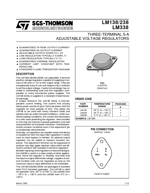
DESCRIPTION
The LM138/LM238/LM338 are adjustable 3-terminal positive voltage regulators capable of supplying in excess of 5A over a 1.2V to 32V output range. They are exceptionally easy to use and require only 2 resistors to set the output voltage. Careful circuit design has resulted in outstanding load and line regulation comparable to many commercial power supplies. The LM138 family is supplied in a standard 3-lead transistor package. A unique feature of the LM138 family is time-dependent current limiting. The current limit circuitry allows peak currents of up to 12A to be drawn from the regulator for short periods of time. This allows the LM138 to be used with heavy transient loads and speeds start-up under full-load conditions. Under sustained loading conditions, the current limit decreases to a safe value protecting the regulator. Also included on the chip are thermal overload protection and safe area protection for the power transistor. Overload protection remains functional even if the adjustment pin is accidentally disconnected. Normally, no capacitors are needed unless the device is situated far from the input filter capacitors in which case an input bypass is needed. An optional output capacitor can be added to improve transient response. The adjustment terminal can be bypassed to achieve very high ripple rejection ratios which are difficult to achieve with standard 3-terminal regulators. Besides replacing fixed regulators ordiscrete designs, the LM238 is useful in a wide variety of other applications. Since the regulator is ”floating” and sees only theinput-to-output differential voltage, supplies of several hundred volts can be regulated as long as the maximum input to input differential is not exceeded.
2SK1530Y中文资料
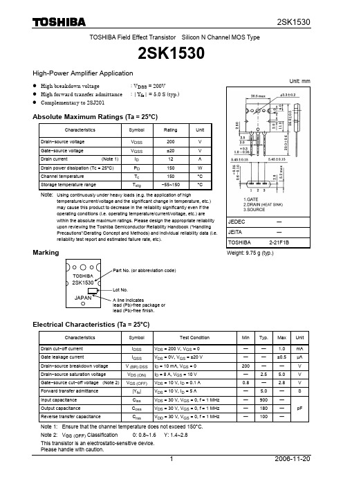
TOSHIBA Field Effect Transistor Silicon N Channel MOS Type2SK1530High-Power Amplifier Applicationz High breakdown voltage: V DSS = 200V z High forward transfer admittance : |Y fs | = 5.0 S (typ.)z Complementary to 2SJ201Absolute Maximum Ratings (Ta = 25°C)Characteristics Symbol Rating UnitDrain −source voltage V DSS 200 V Gate −source voltage V GSS±20 V Drain current(Note 1)I D 12 A Drain power dissipation (Tc = 25°C) P D 150 W Channel temperature T c 150 °C Storage temperature rangeT stg−55~150 °CNote: Using continuously under heavy loads (e.g. the application of hightemperature/current/voltage and the significant change in temperature, etc.) may cause this product to decrease in the reliability significantly even if the operating conditions (i.e. operating temperature/current/voltage, etc.) arewithin the absolute maximum ratings. Please design the appropriate reliability upon reviewing the Toshiba Semiconductor Reliability Handbook (“Handling Precautions”/Derating Concept and Methods) and individual reliability data (i.e. reliability test report and estimated failure rate, etc).MarkingElectrical Characteristics (Ta = 25°C)Characteristics Symbol Test Condition Min Typ. Max UnitDrain cut −off current I DSS V DS = 200 V, V GS = 0 — — 1.0 mA Gate leakage currentI GSS V DS = 0V, V GS = ±20 V — — ±0.5μA Drain −source breakdown voltage V (BR) DSS I D = 10 mA, V GS = 0 200 — — V Drain −source saturation voltage V DS (ON) I D = 8 A, V GS = 10 V — 2.5 5.0 V Gate −source cut −off voltage (Note 2) V GS (OFF) V DS = 10 V, I D = 0.1 A0.8 — 2.8 V Forward transfer admittance |Y fs | V DS = 10 V, I D = 5 A— 5.0 — SInput capacitance C iss V DS = 30 V, V GS = 0, f = 1 MHz — 900 — Output capacitance C oss V DS = 30 V, V GS = 0, f = 1 MHz — 180 — Reverse transfer capacitanceC rssV DD = 30 V, V GS = 0, f = 1 MHz—100—pF Note 1: Ensure that the channel temperature does not exceed 150°C. Note 2: V GS (OFF) Classification0: 0.8~1.6Y: 1.4~2.8This transistor is an electrostatic-sensitive device.Please handle with caution.Unit: mmJEDEC ― JEITA―TOSHIBA 2-21F1B Weight: 9.75 g (typ.)Switching Time Test Circuit WaveformsRESTRICTIONS ON PRODUCT USE20070701-EN •The information contained herein is subject to change without notice.•TOSHIBA is continually working to improve the quality and reliability of its products. Nevertheless, semiconductor devices in general can malfunction or fail due to their inherent electrical sensitivity and vulnerability to physical stress. It is the responsibility of the buyer, when utilizing TOSHIBA products, to comply with the standards of safety in making a safe design for the entire system, and to avoid situations in which a malfunction or failure of such TOSHIBA products could cause loss of human life, bodily injury or damage to property.In developing your designs, please ensure that TOSHIBA products are used within specified operating ranges as set forth in the most recent TOSHIBA products specifications. Also, please keep in mind the precautions and conditions set forth in the “Handling Guide for Semiconductor Devices,” or “TOSHIBA Semiconductor Reliability Handbook” etc.• The TOSHIBA products listed in this document are intended for usage in general electronics applications (computer, personal equipment, office equipment, measuring equipment, industrial robotics, domestic appliances, etc.).These TOSHIBA products are neither intended nor warranted for usage in equipment that requires extraordinarily high quality and/or reliability or a malfunction or failure of which may cause loss of human life or bodily injury (“Unintended Usage”). Unintended Usage include atomic energy control instruments, airplane or spaceship instruments, transportation instruments, traffic signal instruments, combustion control instruments, medical instruments, all types of safety devices, etc.. Unintended Usage of TOSHIBA products listed in his document shall be made at the customer’s own risk.•The products described in this document shall not be used or embedded to any downstream products of which manufacture, use and/or sale are prohibited under any applicable laws and regulations.• The information contained herein is presented only as a guide for the applications of our products. No responsibility is assumed by TOSHIBA for any infringements of patents or other rights of the third parties which may result from its use. No license is granted by implication or otherwise under any patents or other rights of TOSHIBA or the third parties.• Please contact your sales representative for product-by-product details in this document regarding RoHS compatibility. Please use these products in this document in compliance with all applicable laws and regulations that regulate the inclusion or use of controlled substances. Toshiba assumes no liability for damage or losses occurring as a result of noncompliance with applicable laws and regulations.。
2SK2381中文资料

62.5
°C / W
Note 1: Ensure that the channel temperature does not exceed 150°C. Note 2: VDD = 50 V, Tch = 25°C (initial), L = 4.2 mH, RG = 25 Ω, IAR = 5 A Note 3: Repetitive rating: pulse width limited by maximum channel temperature This transistor is an electrostatic-sensitive device. Please handle with caution.
z Low drain−source ON resistance : RDS (ON) = 0.56 Ω (typ.)
z High forward transfer admittance : |Yfs| = 4.5 S (typ.)
z Low leakage current
: IDSS = 100 μA (max) (VDS = 200 V)
1
2006-11-21
Electrical Characteristics (Ta = 25°C)
Characteristics
Symbol
Test Condition
Gate leakage current Drain cut−off current Drain−source breakdown voltage Gate threshold voltage Drain−source ON resistance Forward transfer admittance Input capacitance Reverse transfer capacitance Output capacitance
PCF8583中文资料_带有 256×8bit RAM 的 8 引脚日历时钟芯片

PCF8583中文资料 芯片简介:1、PCF8583是P H IL IPS公司制造的带有256×8bit RAM的8引脚日历/时钟芯片,采用I2C2、两线串行总线接口,内含完整的振荡,分频,上电复位电路,并具备计时,日历,定时,闹钟和中断输出功能.3、日历/时钟芯片I2C总线RAM定时器4、带256字节RAM的实时时钟芯片PCF85831.芯片特点●数据保持和时钟工作电压1~6V ,总线工作电压2. 5~6V ;●采用8脚D IP或SO封装形式;●I2C两线串行总线接口;●内含256×8bit静态RAM ;●有定时,定闹功能和中断输出;●内有振荡器,分频器和上电复位电路,可使用32 768Hz石英晶振或外部50Hz时钟;●片内字节地址读写后自动加一;●可用作定时器或计数器.2.引脚功能PCF8583引脚功能如图1所列.芯片结构图1:3.片内寄存器功能描述在256字节RAM中,前16字节(地址00~0F H)是带有特殊功能的寄存器,现分述如下:内部结构如图2:3. 1状态寄存器(地址00H)状态寄存器控制着芯片所有的功能和操作,其内容如图3所列.图3 PCF8583状态寄存器详细说明如下:00寄存器(状态寄存器)8个位名称功能:0、计时器计时器到标志1闹钟定闹时间到标志查询IC价格,上IC酷搜网http://www.icqoso.com/data-PCF8583T.html 查询IC价格,上IC酷搜网http://www.icqoso.com/data-PCF8583T.html 查询IC价格,上IC酷搜网http://www.icqoso.com/data-PCF8583T.html 2闹钟使能(是否闹钟允许)0:禁止;1 :允许3屏蔽05和06字节屏蔽0 :不屏蔽;1 :屏蔽4~5功能模式芯片工作方式00:32768 Hz时钟;01 :50 Hz时钟;10 :计数器模式;11 :测试模式6计数锁存0:计数;1 :锁存7计数停止停止计数标志0:计数;1 :停止计数,分频器复位3. 2时钟计数器(地址01H~06H)查询IC价格,上IC酷搜网http://www.icqoso.com/data-PCF8583T.html 通过设置状态寄存器,可以选择32 768Hz和50Hz时钟模式或计数器模式.各时钟计数器功能如图4-7所列.1/ 100秒,秒,分,小时依次在地址01~04H.年以0~3表示,0为闰年.小时计数器的高2位分别作为12小时或24小时模式选择(0为24h , 1为12h)和上下午指示(0为AM ,1为PM).年份和日期,星期和月份分别在地址05H和06H.如果状态寄存器的屏蔽位有效,当读这些寄存器时,年份和星期的有关位会被屏蔽,这样允许用户直接读取日期和月份.在芯片以计数器方式工作时,计数器对振荡器输入端的脉冲计数,最多可达到6位数.以BCD码格式依次放在地址01~03H中,此时分频器无效.08寄存器(控制寄存器)8位使用说明:(2种模式,由00寄存器4-5位来控制)图8 时钟和日历计数器(时钟方式)地址bit7bit6bit5bit4~0011/ 100秒(0~99)02秒(0~59)03分(0~59)0424/ 12hAM/ PM 小时(0/ 1~24/ 12)05年(0~3)日期(1~28/ 29/ 30/ 31)06星期(0~6)月(1~12)07计时器(0~99)08闹钟控制寄存器09闹钟1/ 100秒0A 闹钟秒0B 闹钟分0C 闹钟小时0D 闹钟日期0E 闹钟月份查询IC价格,上IC酷搜网http://www.icqoso.com/data-PCF8583T.html 查询IC价格,上IC酷搜网http://www.icqoso.com/data-PCF8583T.html 0F闹钟计时器在设置时间时,应设置状态寄存器的停止位停止时钟,否则可能导致时钟混乱.3. 3计时器(地址07H)设置状态寄存器为XX0XX1XX可以打开计时器.在时钟模式中,计时器可以编程为以1/ 100秒,秒,分,小时或天计数.缺省状态下,计时器按天数累计.计时器为百进计数,溢出时,timer标志被置位,这个标志必须由软件来复位,通过设置闹钟寄存器的计时器中断允许位,可以传递到IN T脚引起中断.计时器的分辨率可通过设置定闹寄存器的低3位来编程(如表4所列).3. 4闹钟控制寄存器(地址08H)闹钟控制寄存器是用来控制定闹,定时和中断输出功能的.在时钟和计数器方式下有不同的功能(如表4所列).3. 5闹钟寄存器(地址09H~0F H)设置状态寄存器可以激活闹钟寄存器.设置闹钟控制寄存器可以选择定闹方式,闹钟时间到会使状态寄存器中的alarm标志置高,当alarm中断允许标志为1时,输出IN T引脚被拉低,并一直保持到复位或被软件清除.闹钟寄存器以时钟计数器相同的顺序放在地址09H以后的位置上(如表3所列),当闹钟寄存器每位都符合对应的时钟计数器时产生一个闹钟信号.通过设置闹钟计数器,闹钟可以被编程为控制日期,每天,每周或一段时间后启动;指定日期的闹钟忽略年和周位;日闹钟忽略月和日期位;周闹钟时,周/月寄存器将选择一周相应的一天启动闹钟,此时闹钟月份寄存器(0EH)改为星期寄存器,低七位对应周日到周六,最高位不用.另外,通过设置计时报警位,可以编程为定时闹钟.当计时器(0F H)值和时钟计数器(07H)位相同时,报警启动(alarm标志置1).在12小时模式时,第6和第7位的时寄存器一样.3. 6计数器的模式状态寄存器为XX10XXXX 时,可以选择计数器模式,计数器模式仅使用RAM 的01H~03H 字节,用于对O SC I 端脉冲的计数(O SCO 开路).计数器最大可计到百万(6位BCD 码).如允许计数报警,当计数器的值与09H,0A H,0B H 位的值相同时将发生一次计数报警, alarm 标志被置1 ,设置中断允许可引发中断.在此模式下,计时器(07H)受报警控制寄存器低3位控制,计时器的功能和时钟模式相同.4.芯片其它功能4. 1中断输出IN T 端图10 闹钟控制寄存器bit 名称时钟功能计数器功能0~2timer计时器设置000:无计时器001 :1/ 100秒查询IC价格,上IC酷搜网http://www.icqoso.com/data-PCF8583T.html 010 :秒011 :分100 :小时101 :日110 :不用111 :测试模式计时器设置000:无计时器001 :1010 :100011 :10000100 :1000000101 :禁止110 :禁止111 :测试模式3timer IN Tenable计时器中断允许0:禁止 1 :允许计时器中断允许0:禁止 1 :允许4~5alarm时钟定闹设置00:无闹钟01 :日期闹钟10 :周闹钟11 :每日闹钟定闹设置00:无定闹01 :定闹方式10 ,11 :禁止6timer alarm enable计时器报警允许 0:禁止 1 :允许计时器报警允许0:禁止 1 :允许7alarmIN Tenable报警中断允许0:禁止 1 :允许报警中断允许0:禁止 1 :允许与89c5252连接图,定时int输出控制cpu外部中断0 唤醒休眠中的cpu也可一唤醒掉电的cpu。
飞利浦闪系列筒射灯产品尺寸和规格

5W=325/346lm
整体寿命
高达20,000hrs
高达15,000hrs
高达15,000hrs
灯光角度
100°
24°
瓦数
3.5W/5W/5.5W/6.5W/7W/8W/9W
3W,5W
灯光色温
2700K,4000K,6500K
2700K,4000K
灯具尺寸(mm)
W*D*H
80080=2.5″
66020=2.5″
44080=2.5″
47030=2.5″
80081=3″
80081=3″
66021=3″
44081=3″
47031=2.5″
80082=3.5″
80082=3.5″
66022=3.5″
44082=3.5″
47032=2.5″
80083=4″
80083=4″
66023=4″
ø94*63mm
ø92*63mm
ø92*58mmቤተ መጻሕፍቲ ባይዱ
ø84*43mm
ø105*66mm
ø105.5*66mm
ø105*61mm
ø120*69mm
ø120*69mm
ø120*61mm
ø139*77mm
ø135*70mm
ø135*63mm
CRI显色指数
>80
>80
散热设计
Yes
No
低眩光
Yes
No
飞利浦闪系列筒射灯产品尺寸和规格
飞利浦闪系列LED灯凭借创新技术、优越性能,在市场上赢得了良好的口碑,受到越来越多消费者的青睐。为了让大家在选购筒灯、射灯的时候,能对飞利浦闪系列有个全面的了解看,现将飞利浦闪系列筒射灯产品参数归纳如下。
1808382资料
Extract from the online catalog
SMSTB 2,5/ 6-ST BK AU://eshop.phoenixcontact.de/phoenix/treeViewClick.do?UID=1808382
AWG/kcmil UL Nominal voltage UN Nominal current IN AWG/kcmil Certification
30-12
300 V 10 A 30-12 CSA, CUL, UL
PHOENIX CONTACT GmbH & Co. KG http://www.phoenixcontact.de
CSA Nominal voltage UN Nominal current IN AWG/kcmil CUL Nominal voltage UN Nominal current IN 300 V 10 A 300 V 10 A 28-12
PHOENIX CONTACT GmbH & Co. KG http://www.phoenixcontact.de
Product notes Commercial data EAN Pack Customs tariff Weight/Piece 4017918214760 50 Pcs. 85366990 0.0116 KG http:// Please note that the data given here has been taken from the online catalog. For comprehensive information and data, please refer to the user documentation. The General Terms and Conditions of Use apply to Internet downloads. Certificates / Approvals WEEE/RoHS-compliant since: 01/01/2003
材料规格转换

14121411Technical DataComparison of Materials between JIS and Foreign Standards 2NFZ2CND17.12Heat resisting steel plate Heat resisting steel bar JIS G 4311 4312 4317 4313 4315,JIS G 4317 4313 4315,JIS G Notes 1 Specified by ISO 4954Notes 2 Because the type number is not specified, the UNS number is designated.As for ISO codes, the source of SUS 630 and SUS 631 is ISO 683/XVI, and the source for the others is ISO 683/XIII. The SUH group is mostly based on ISO 683/XV except for SUH 409 which is based on 683/XIII.BHMOCT20X12OCT40X10C2M OCT40X9C2 OCT20X25H20C2 OCT5X20 9AH4OCT09X17H71 O OCT14X17H2 OCT30X13OCT20X13 OCT08X13 OCT12X13NFZ20CDNbV11NFZ45CS9NFZ80CSN20.02NFZ40CSD10NFZ45CS9NFZ10C24NFZ6CT1225.15B NFZ6NCTDVNFZ12.NCS35.16NFZ12CN25.20NFZ15CN24.13NFZ52CMN21.09NFZ35CNWS14.14NFZ8CNA17.7NFZ6CNU17.04NFZ100CD17NFZ15CN16 02NFZ30CF13NFZ30C13NFZ20C13NFZ12CF13NFZ6C13NFZ13C13BS443S65BS401S45BS409S19BS310S24BS309S24BS381S34BS349S54BS349S52BS331S42BS431S29BS420S45BS420S29BS416S21BS403S17BS403S21ASTM616AISI446AISI409ASTM661ASTM660AISI330AISI310AISI309ASTM631ASTM630ASTM440F AISI440C AISI440B AISI440A AISI431AISI420FAISI420AISI416ASTM410S AISI 410AISI 4034211Ti 1279852( )1( )A 1b 9b 54713A 2SUH616SUH600SUH11SUH4SUH3SUH1SUH446SUH409SUH21SUH661SUH660SUH330SUH310SUH309SUH38SUH37SUH36SUH35SUH31SUS 631SUS 630SUS 440F SUS 440C SUS 440B SUS 440A SUS 431SUS 429J1SUS 420FSUS 420J2SUS420J1SUS416SUS 410J1SUS410S SUS 410SUS 403OCT12X17OCT08X18H12B OCT08X18H10T OCT03X17H14M2OCT03X18H11OCT08X18H10 OCT12X18H10EOCT12X17 9AH4NFZO1CD26.1NFZ8CD17.01NFZ8CNb17NFZ8CT17NFZ10CF17NFZ8C17NFZ3C14NFZ6CA13NFZ15CNS20.12NFZ6CNU18.10NFZ6NC18.16NFZ6CNNb18.10NFZ6CNT18.10NFZ2CND19.15 AzNFZ2CND17.12NFZ6CND17.11NFZ12CN25.20NFZ10CN24.13NFZ8CN18.12NFZ2CN18.10Az NFZ5CN18.09Az NFZ2CN18.10NFZ6CN18.09NFZ10CNF18.09NFZ10CN18.09NFZ12CN17.07BS434S17BS430S17BS405S17BS347S31BS321S31BS317S12BS317S16BS316S11BS316S31BS305S19BS304S11BS304S31BS303S41BS303S21BS302S25BS301S21BS284S16F19c 8a 82D32(1)D25(1)16152419N ,19aN 19,19a20,20a 1310N 101117a 171214A 3A 2SUSXM27SUS 447J1SUS 444SUS 436L SUS 434SUS 430LX SUS 430F SUS 430SUS 429SUS 410L SUS 405SUS 329J2L SUS 329J1SUSXM15J1SUSXM7SUS 384SUS 347SUS 321SUS 317J1SUS 317L SUS 317SUS 316J1L SUS 316J1SUS 316LN SUS 316N SUS 316L SUS 316SUS 310S SUS 309S SUS 305J1SUS305SUS 304LN SUS 304N2SUS304N1SUS304L SUS304SUS303Se SUS303SUS 302BSUS 302SUS 301J1SUS 301SUS 202SUS 201ASTMXM27S44400ASTM (2)AISI 434ASTMXM8AISI 430F AISI 430AISI 429AISI 405S32550S31803ASTM (2)AISI 329ASTMXM15ASTMXM7AISI 384AISI 347AISI 321AISI 317L AISI 317 LNASTM316AISI 316NAISI 316L AISI 316AISI 310SAISI 309SAISI 305LN ASTM304ASTMXM21AISI 304N AISI 304L AISI 304AISI 303Se AISI 303AISI 302B AISI 302AISI 301AISI 202AISI 201Japan Industrial Standards CodeSteel Type Related to Foreign Standards OCT 5632Standard NumberNameI 683/683/I A I S I ASTMB S 1449Part4970Part4B S DIN 17440DIN17224NFA35 573 584NFA35 586NFA35 586NFA35 573 584DIN 17224DIN 17440B S 970Part41449Part4B SASTMA I S I NameStandard NumberOCT 5632DIN 17441Steel Type Related to Foreign StandardsCodeJapan Industrial Standards Stainless Steels/Heat Resisting Steels and Related MaterialsSteel Brands Comparison Table105V 1140C 2 701 701 801 801 901 9011051120214028575 Z35CWDV5Y 9Y8 Special purpose steels High carbon-chrome bearing steel JIS G 4805JIS G 4804Sulfur andsulfur combined free cuttingsteel JIS G 4404Alloy tool steel High-speed tool steelJIS G 4403NameStandard Number Name Standard NumberStandard Number60C2 60C2X15 80 X A50X A 50X S250Pb 55CrV455C3100C6(45MF6.3)(45MF6.1)(35MF 6)(13MF 4) S300Pb S250(RH 388)527A60535A99 226M44 230M07220M07 735A50527A60250A61250A58250A53Grade 1ASTMA4855210051100114411411137 111712L14 121512L13121312221108111041619254 6150926010781075SUJ5SUJ 4SUJ 3SUM23SUJ2SUJ 1SUM43SUM42SUM41SUM32SUM31LSUM31SUM25SUM24L SUM23SUM22L SUM22SUM21SUM12SUM11SUP13SUP12SUP11A SUP10SUP 9A SUP 9SUP 7SUP6SUP 309 08 04 02 0109 04 02 0210 10 04 04 0306 05 05 04 0206 05 04 0406 05 04 0306 05 04 0212 05 05 0418 05 04 0118 10 04 0218 04 01Z90WDKCVZ160CDV12Z200C12 105WC13 Y Y 105WC13 Z110DKCWVZ100DCWV Z130WKCDVZ130DCV Z120WDCVZ85WDCVZ160WKCVZ80WKCVZ80WKCVZ80WCV Y Y Y Y Y SKD12SKD 4SKD 5SKD 6SKD61SKD62SKD 7SKD 8SKT 3SKT 4H19H10H12H13H11H21 A2 BH19BH10BH12BH13BH11BH21 BA 2Z100CDV5Z32WCV5Z30WCV9Z38CDV5Z40CDV532DCV2855CNDV455NCDV75XHM 3X3M3 4X5M 1C 4X5M C Y13Y12Y11Y10Y 8Y 7P18 P6M5K5 XB4 13X 9XB XB X12Y Y Y Y BW1C BW1B BW1A BW1A BT 1BT 4BT 5BT15BM 2 BM 4 BM42BW 2 BD 3BD2W1 13W1 111/2W1 10W1 9W1 8W1 7 T 1T 4T 5T15M 2M3 1M3 2M 4 M36 M 7M42F 2 L 6 W2 91/2W2 81/2D 3D 2SKD11SKD 1SKS95SKS94SKS93SKS31SKS3SKS44SKS43SKS41SKS4SKS8SKS 7SKS51SKS 5SKS21SKS2SKS11SKH59SKH58SKH57SKH56SKH55SKH54SKH53SKH52SKH51SKH10SKH4SKH3SKH2SK7SK6SK5SK4SK3SK2SK1Spring steelJIS G 4801Japan Industrial Standards CodeAISISAE BSSteel Type Related to Foreign StandardsDIN NF OCT(Continued )JIS G 4404ASTM OCTNF BS AISICodeSteel Type Related to Foreign StandardsJapan Industrial StandardsNameDINVDEhVDEh DIN Tool Steels and Related MaterialsJapan Industrial Standards Steel Type Related to Foreign Standards Code AISIBS NF OCTASTM JIS G 4401Carbon tool steelS S O O4303 4309,S O I 683/683/S O I 4303 4309, P ClassificationAlloy tool steelHigh speed tool steelP/M high speed steelPre hardened steelFlame-hardened steel Cold, highly hardened steelSteel Types Related to the Foreign Standards JIS AISI DIN Steel Maker and Brand NameHitachi Metals, Ltd.Daido Steel Co.,Ltd.Uddeholm Kobe Steel Co.,Ltd.Aichi Steel Works,Ltd.NACHI SKS93SKS3SKS31SKD1SKD11SKD12A2D2D3X210Cr12SKH51SKH55SKH57SKH57 Modification )SKD11 Modification S6 5 2S6 2 5S10 4 3 10S9 2 2 8 1.20801.23791.33431.23631.32431.32071.324755 6255 62SKD11 8Cr group58 63SKD11 8Cr group modification55 6255 6557 6555 6857 6857 6661 6558 6664 6866 6969 721330 33P21 groupPrecipitation hard-ening steel group P20 group M2M35M42T15PMS50C group SCM group36 42SKD61 Modification SKS group48 5155 6255 62YCS3SGTCRD SLDSLD8SCD YK30GOA DC1DC11DC53DC12GO31MH85MH24MH8MH64MH57MH55MH51DEX20PDS1PXZDEX70/80DEX61DEX40PX5NAK55NAK80HPM1HPM50GO40F HPM2T DH2F FDAC CX1HPM2HPM7HAP40HAP50HAP72HAP1058 62DEX-M1HAP5R FAX18YXR3YXR7YXM60YXM1YXM4XVC5YXR1RIGOR ARNE SVERKER21SVERKER3SKS31SKS31SKD12SKD11AUD15SKD1CDS1CDS11SKS3SK301KS31KD12KD21KD11S KD11KD1KS3SKS3K3M H51QH51SKH9HM35HM35MV10HS93R KDMV QHZ MCR1MDS3HS97RHM9TLHS98M ASP23ASP30ASP60KHA32/77SPM23FAX31KHA30SPM30FAX38KHA50SPM60FAX40/G2KHA60SPM75FAXG1KTSM2A KTSM3M KTSM21/22ASSAB618IMPAXUHB11KTSM40EAUD61KTSM40EF KPM1KPMAX KPM30KAP1KAP2KDASS PCM40QD6F GO5HMD5FERMOSX105V FH5GO4ACD37AKS3KSM QF3Hardness in Use HRC SKH5957 62Matrix groupNippon Koukan Steel Co.,Ltd.Sanyo Special Steel Co., Ltd.SK3MQK3M QKS3QC1QC11QCM8CDS12MCR12ARK1DCXMDS910203040506070MaterialsMachined MaterialsNonferrousMetalUntreated Thermal RefinedQuenched/TemperedEquipmentNC milling cutter General purpose mill-ing cutter Machining center Drilling machine Jig borerDrill pressBoring machineNC latheGeneral purpose lathe Turning center Jig grinder Surface grinder Forming grinderCylindrical grinderProfile grinder E D MW E D MTaps Magnets grindstoneElectrode master WireDrills Cutting tools Reamers End mills Drills Cutting toolsTaps Reamers DrillsCutting toolsReamers TapsMagnets grindstone Drills ReamersEnd milsCuttingtoolsElectrode master WireCarbon tool steel Cemented carbide Special tool steel High-speed steel High-speed steel Special tool steel Cemented carbide Carbon tool steel Carbon tool steel Special tool steel High-speed steel Cemented carbide Boron DiamondElectrodeposited boron Black silicon carbide Green silicon carbide Pink fused alminaBrown fused alumina White fused alumina Electrodeposited diamondElectrolytic copper BrassCopper tungsten Silver tungstenBrass TungstenWnCU Zn Wn CU D WA A PAGC CCBN DCBN Wn CoSKH SKS SKSK Wn Co SKS SKH SKH SKS Wn Co SK S45C (AI alloi )(SKD12group )SS400(SS41) SKD11S50C DC53SKD61(AI )CU BsBM2HRC(Be Cu )SCM435HPM2THPM7 NAK55PX5 HPM1NAK80HPM38 HPM50DH2F S45C SKS3 SUJ2(SKD12group )SKH51DC53 (Carbide )SKD11HPM38()MAS1C hardened Age-(Nonferrous metal )(Nonferrous metal )(Nonferrous metal )(Carbide )(Carbide )are registered trademarks of UDDEHOLM TOOL CO.and S-STAR FDAC SKD61S-STARHardness of Material and Corresponding ToolsSteel Brands Comparison Table Hardness of Material and Corresponding ToolsProcessing MethodRequired ToolsToolsParts MaterialsFor Press DieFor PlasticMold Tools MaterialsCutting GrindingElectroerosionBoring on Flanks and BottomBoring Machining CylindersElectroforming /outside Electroforming /insideStainless steel strips in coil Stainless steels Equal leg angle steelsStainless steel wires Stainless steel wires for spring for springfor cold forgingStainless steel wires Stainless steel wires Stainless steel plates Stainless steel plates Hot rolledStainless steel plates Cold rolledCold rolledStainless steel plates Hot rolledHot rolled Stainless steel bars 181018164171221713217122DINX6CrNb17DINX6CrTi17DINX12CrMoS17DINX6Cr17DINX6CrAI13DINX6CrNiNb DINX6CrNiTi1810DINX2CrNiMo DINX2CrNiMoNDINX2CrNiMo DINX5CrNiMo DINX5CrNi1812DINX2CrNiN1810DINX2CrNi1911DINX5CrNi1810DINX10CrNiS189DINX12CrNi1771.43711.43101.69001.69001.43051.43011.43061.43111.43031.43031.48331.48451.44491.44381.45501.45671.44601.40021.40161.41041.41131.41311.40011.4401/1.44361.4404/1.44351.4406/1.44291.4878/1.45411.4501/1.4511 X210Cr12 105WCr6105WCr6 S2 10 1 8 S10 4 3 10 S6 5 2 5 S6 5 3 S6 5 2S18 1 2 5 C 70W2C 80W1C 80W1 C105W11.16731.16631.16451.16251.16251.17401.33551.32551.32651.33441.33431.33441.32431.3207 1.32471.25621.24191.25151.24421.20081.28331.24191.24191.20801.2379 DINX6CrTi12DINCrI1205DINCrNi2520DINX7CrNiAI177DINX20CrNi72DINX30Cr13DINX20Cr13DINX6Cr13DINX10Cr131.40001.40061.40001.40211.40051.40211.40281.40571.41121.45421.45681.41251.48711.48711.48281.48411.48641.49441.49711.47421.47201.47621.47181.47311.47471.49351.4873 X38CrMoV51X40CrMoV51 X32CrMoV33 55NiCrMoV61.23631.25671.25811.23431.23441.26061.27139SMn28100Cr655Cr350CrV4 9S209SMnPb281.50281.50281.07151.07361.07231.20571.2067/1.35051.21271.35051.12621.71761.81591.7138 1.07021.07021.07111.07181.07181.7176。
THAT2155资料
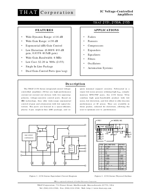
Min
+5 -5
2151 Typ Max
+12 -12 2.4 175 +15 -15 4 750
Min
+5 -5 — —
2150A Typ Max
+12 -12 2.4 175 +15 -15 4 750
Min
+5 -5 — —
2155 Typ Max
+12 -12 2.4 125 +15 -15 4 550
-15V
-15V
Figure 3. Typical Application Circuit
Figure 4. Frequency Response Vs. Gain (2150A)
Figure 5. Noise (20kHz NBW) Vs. Gain (2150A)
THAT Corporation; 734 Forest Street; Marlborough, Massachusetts 01752; USA Tel: (508) 229-2500; Fax: (508) 229-2590; Web:
Units
V V mA µArms
VCC-VEE= 24 V ISET= 2.4 mA
— —
Electrical Characteristics 2
Parameter
Supply Current Equiv. Input Bias Current Input Offset Voltage Output Offset Voltage
Symbol
ICC IB VOFF(IN) VOFF(OUT)
Conditions
No Signal No Signal No Signal Rout=20 kΩ 0 dB gain +15 dB gain +40 dB gain
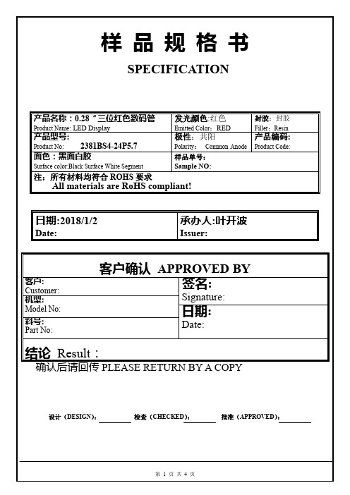
2381BS4-24P5.7
the body.
第3页共4页
5 . 光电特性曲线(Typical Electro optical Characteristics Curve):
第4页共4页
4.保存和焊接条件(Storage & Soldering Conditions):
Store dition ● 注意保存,保存条件不好时,会降低膜片
will decrease the adhesive power between the reflector and film. 与反射壳(导光板)的粘附力。
60
20
5
-20 → +85 -20 → +85
单位(Unit)
mW mA mA V ℃ ℃ V
*焊接温度(Lead Soldering Temperature):260℃ for 3 seconds
*当工作温度高于 25℃时,Ifm,、Ifp、Pd 必须降低;电流降低率是-0.36mA/℃(直流驱动),或-0.86mA/℃(脉 冲驱动)功耗降低率是-0.75mW/℃。 The Ifm Ifp & Pd must be decreased once the temperature is over 25 ℃;the Current decrease rate is: –0.36mA/℃ (Direct Current); -0.86mA/℃ (Pulse drive) the power dissipation is -0.75mW/℃
IF=20mA VR = 5V IF=20mA IF=20mA
VF
1.7
IR
-
λD
620
2θ1/2
-
Type
-
FSS238资料
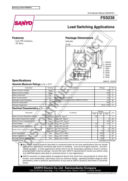
[FSS238]
8 5
0.3 4.4 6.0
5.0
1.5
Specifications
Absolute Maximum Ratings at Ta = 25˚C
Parameter Drain-to-Source Voltage Gate-to-Source Voltage Drain Current (DC) Drain Current (pulse) Allowable Power Dissipation Channel Temperature Storage Temperature Symbol VDSS VGSS ID IDP PD Tch Tstg
100 7 5 3 2 10 7 5 3 2 1.0 7 5 3 2 0.1 7 5 3 2
yfs -- ID
VDS=10V
100 7 5 3 2
IF -- VSD
VGS = 0
= Ta
--2
5°
C
7 C 5°
Forward Current, IF – A
10 7 5 3 2 1.0 7 5 3 2 0.1 7 5 3 2
Switching Time Test Circuit
VDD=15V 10V 0V VIN ID=14A RL=1.07Ω VIN
D
PW=10µs D.C.≤1%
VOUT
G
P.G
50Ω
S
FSS238
6.0V
20 18 16
ID -- VDS
4.0V
20 18
ID -- VGS
VDS=10V
8.0V
3.5
V
V
Drain Current, ID – A
西蒂安姆LED驱动器数据表说明书

Xitanium track adaptor drivers (3C)Xitanium 42W/a 0.3-1.05A 42V 3CW 230V9290 021 29606Affordable and reliable LED DriversAffordable LED driver range offering Philips reliability. The Xitanium track driver range is compatible with COB and mid-power LEDs from any LED manufacturer.Benefits•Driver design based on Philips experience and knowledge of conventional fluorescent and HID technologies•Various power ratings matching common lumen packages/applications•Track adaptor housing design for compact track luminaire designsFeatures •Compact size•Specific, optimized dual-output current choice •Long lifetime•Low output current ripple, low input current THD •Suitable for 3-phase track systems•Available in white, black and grey housing colorApplication•Public buildings (airports, cinemas,theaters, exhibition halls)•Retail (supermarkets, shops)•OfficesAugust 2021Electrical input dataSpecification item Value Unit ConditionRated input voltage range220...240V ac Performance rangeRated input voltage230V acRated input frequency range50...60Hz Performance rangeRated input current0.22A@ full output power @ rated input voltageMax. input current0.25A@ rated output power @ minimum performance input voltage Rated input power50W@ rated output power @ rated input voltagePower factor0.9@ full output power @ rated input voltageTotal harmonic distortion20%@ rated output power @ rated input voltageEfficiency87%@ratedinputvoltage@************************* Input voltage AC range198...264V ac Safety operational rangeInput frequency AC range45...66Hz Safety operational rangeIsolation input to output SELVElectrical output dataSpecification item Value Unit ConditionRegulation method Constant CurrentOutput voltage10...42V dcOutput voltage max.60V Maximum output voltage (rms)Output current0.3...1.05AOutput current tolerance ±5%Output current ripple LF≤ 4%Ripple = peak / average, < 3kHzOutput P st LM≤ 0.06Output SVM≤ 0.07Output power11...42WElectrical data controls inputSpecification item Value Unit ConditionControl method Fixed Set output current via SimpleSet (AOC)Wiring and ConnectionsSpecification item Value Unit TypeOutput wire cross-section0.5...1.5 / 20...16mm2 / AWG solid / stranded wireOutput wire strip length7.5...8.5mmMaximum cable length0.3m Total length of wiring including LED module, one wayInsulationInsulation per IEC61347-1Input OutputInput SELVOutput SELVDimensions and weightSpecification item Value Unit Tolerance (mm)Length (A1)224mmMounting hole distance (A2)112mmWidth (B1)31mmHeight (C1)43.8mmHeight (C2)13.7mmMounting hole diameter (D1)27.3mmMounting hole diameter (D2)24.4mmWeight160gramHousing color White (RAL 9003)Logistical dataSpecification item ValueProduct name Xitanium 42W/a 0.3-1.05A 42V 3CW 230VEOC871869973472500Logistic code 12NC9290 021 29606EAN1 (GTIN)8718699734725EAN3 (box)8718699734732Pieces per box40Operational temperatures and humiditySpecification item Value Unit ConditionAmbient temperature-20...+35ºC Higher ambient temperature allowed as long as Tcase-max is notexceededTcase-max85ºC Maximum temperature measured at T case-pointTcase-life85ºC Measured at T case-pointMaximum housing temperature130ºC In case of a failure, inherent by designRelative humidity10...90%Non-condensingLifetimeSpecification item Value Unit ConditionDriver lifetime50,000hours Measured temperature at Tcase-point is Tcase-life. Maximumfailures = 10%Storage temperature and humiditySpecification item Value Unit ConditionAmbient temperature-25...+85ºCRelative humidity 5...95%Non-condensingProgrammable featuresSpecification item Available Default setting ConditionSet Adjustable Output Current (AOC)SimpleSet300 mAOEM Write Protection (OWP)Yes OFFLuminaire Info (DALI part 251)Yes —FeaturesSpecification item Value ConditionOpen load protection Yes Automatic recoveringShort circuit protection Yes Automatic recoveringOver power protection Yes Automatic recoveringHot wiring NoSuitable for fixtures with protection class I per IEC60598Inrush currentSpecification item Value Unit ConditionInrush current14A Input voltage 230VInrush peak width255µs Input voltage 230 V, measured at 50% heightDrivers / MCB 16A type B≤ 36pcs Indicative valuePlease refer to the driver design in guide if you use other MCB-types.Driver touch current / protective conductor currentSpecification item Value Unit ConditionTypical Touch Current (ins. Class II)0.7mA peak Acc. IEC61347-1. LED module contribution not includedSurge immunitySpecification item Value Unit ConditionMains surge immunity (diff. mode)1kV Acc. IEC61000-4-5. 2 Ohm, 1.2/50us, 8/20usMains surge immunity (comm. mode)2kV Acc. IEC61000-4-5. 12 Ohm, 1.2/50us, 8/20usApplication InfoSpecification item ValueApproval marks CE / CQC / EAC / ENEC / RCM / SELV / UAIngress Protection classification (IP)20Application Indoor PointMounting Type Track mountingGraphsOperating windowPower factor versus output powerEfficiency versus output powerTHD versus output powerNotesThe adapter is compatible with Global Trac Pro, Stucchi OneTrack 3 Circuit tracks.©2021 Signify Holding, IBRS 10461, 5600 VB, NL. All rights reserved.UK importer address: Signify Commercial UK Limited, 3, Guildford Business Park, GU2 8XG.The information provided herein is subject to change without notice. Signify does not give any representation or warranty as to the accuracy orcompleteness of the information included herein and shall not be liable for any action in reliance thereon. The information presented in this documentis not intended as any commercial offer and does not form part of any quotation or contract, unless otherwise agreed by Signify.Philips and the Philips Shield Emblem are registered trademarks of Koninklijke Philips N.V. All other trademarks are owned by Signify Holding or theirrespective owners.Date of release: August 25, 2021 v3/oem。
2SC2383中文资料(toshiba)中文数据手册「EasyDatasheet - 矽搜」

(V)
0.1
Collector-emitter saturation voltage
CE (sat)
IC/IB = 10
V 0.05
5 0.03
0.01
5 10
30
100
300
1000
Collector current I C (mA)
VCE (sat) – IC
0.5
Common emitter 0.3 IC/IB = 10
• 产品适用于一般电子应用(如电脑,个人设备,办公设备,测量设备,工业机器人和家用电子电器)或特定的应用,明确本文中提到的使用.
产品既不打算,也没有必要使用设备或需要非常高水平的质量和/或可靠性和/或故障或失败的系统,其中可能造成的生命损失,人身伤害,重大财产损 失或严重的公众影响( “误用”).非预期使用包括,但不限于核设施使用的设备,在航空航天工业中使用的设备,医疗设备,用于汽车,火车,轮船 等运输,交通信号设备,用于控制发火或爆炸装置,安全装置的设备,电梯和自动扶梯,涉及到电力设备,以及设备在金融相关领域.不要使用产品的 误用,除非本文档中的特别许可.
0.005
3
10
30
100
300
Collector-emitter voltage V CE (V)
4
2009-12-21
芯片中文手册,看全文,戳
2SC2383
限制产品用途
• 东芝公司及其子公司和附属公司(统称为“TOSHIBA”),保留对本文档的更改信息的权利,以及相关的硬件,软件和系统(统称为“产品”),恕不另行通 知.
1 ms* 10 ms*
0.1 Collector current I
1808858资料

Extract from the onlinecatalogMSTBC 2,5/ 6-ST-5,08Order No.: 1808858The illustration shows a 15-position versionhttp://eshop.phoenixcontact.de/phoenix/treeViewClick.do?UID=1808858Plug component, nominal current: 12 A, rated voltage: 320 V, pitch:5.08 mm, no. of positions: 6, type of connection: Crimp connectionhttp://Please note that the data givenhere has been taken from theonline catalog. For comprehensiveinformation and data, please referto the user documentation. TheGeneral Terms and Conditions ofUse apply to Internet downloads. Technical dataDimensions / positionsPitch 5.08 mmNumber of positions6Technical dataInsulating material group IRated surge voltage (III/3) 4 kVRated surge voltage (III/2) 4 kVRated surge voltage (II/2) 4 kVRated voltage (III/2)320 VRated voltage (II/2)630 VConnection in acc. with standard EN-VDENominal current I N12 ANominal voltage U N320 VNominal cross section 2.5 mm2Maximum load current12 AInsulating material PAInflammability class acc. to UL 94V0Connection dataConductor cross section stranded min.0.5 mm2Conductor cross section stranded max. 2.5 mm2Conductor cross section AWG/kcmil min.20Conductor cross section AWG/kcmil max14Certificates / ApprovalsCSANominal voltage U N300 VNominal current I N10 AAWG/kcmil20-14CULNominal voltage U N300 VNominal current I N10 AAWG/kcmil20-14ULNominal voltage U N300 VNominal current I N10 AAWG/kcmil20-14Certification CB, CSA, CUL, UL, VDE-PZIAccessoriesItem Designation DescriptionMarking0804293SK 5,08/3,8:FORTL.ZAHLEN Marker card, printed horizontally, self-adhesive, 12 identicaldecades marked 1-10, 11-20 etc. up to 91-(99)100, sufficient for120 terminal blocksPlug/Adapter1734634CP-MSTB Coding profile, is inserted into the slot on the plug or invertedheader, red insulating material3190564MSTBC-MT 0,5-1,0Module female contact, is inserted into the plug housing MSTBCafter crimping the conductor, for conductors from 0.5 to 1.0 mm²3190645MSTBC-MT 0,5-1,0 BA Module female contact, is inserted into the MSTBC connectorshell after the conductor has been crimped, for conductors from0.5 - 1.0 mm², ribbon contact3190551MSTBC-MT 1,5-2,5Module female contact, is inserted into the plug housing MSTBCafter crimping the conductor, for conductors from 1.5 to 2.5 mm²3190658MSTBC-MT 1,5-2,5 BA Module female contact, is inserted into the MSTBC connectorshell after the conductor has been crimped, for conductors from1.5 -2.5 mm², ribbon contactTools1204038CRIMPFOX MT 2,5Crimping pliers, for crimping conductors to the module femalecontacts STG-MTN, crimp range: 0.5-2.5 mm², AWG: 20-14 1205037SZS 0,4X2,5Screwdriver, bladed, matches all screw terminal blocks up to 1.5mm² connection cross section, blade: 0.4 x 2.5 mm Additional productsItem Designation DescriptionGeneral1880342EMSTBA 2,5/ 6-G-5,08Header, nominal current: 12 A, rated voltage: 250 V, pitch: 5.08mm, no. of positions: 6, mounting: press in1859551EMSTBVA 2,5/ 6-G-5,08Header, nominal current: 12 A, rated voltage: 200 V, pitch: 5.08mm, no. of positions: 6, mounting: Press in1873391FKIC 2,5/ 6-ST-5,08Plug component, nominal current: 12 A, rated voltage: 320 V,pitch: 5.08 mm, no. of positions: 6, type of connection: Spring-cage connection1823888ICC 2,5/ 6-STZ-5,08Plug component, nominal current: 12 A, rated voltage: 250 V,pitch: 5.08 mm, no. of positions: 6, type of connection: Crimpconnection1762415MDSTB 2,5/ 6-G1-5,08Header, nominal current: 10 A, rated voltage: 250 V, pitch: 5.08mm, no. of positions: 6, mounting: Soldering1842102MDSTBA 2,5/ 6-G-5,08Header, nominal current: 10 A, rated voltage: 250 V, pitch: 5.08mm, no. of positions: 6, mounting: Soldering1762541MDSTBV 2,5/ 6-G1-5,08Header, nominal current: 10 A, rated voltage: 250 V, pitch: 5.08mm, no. of positions: 6, mounting: Soldering1770753MSTB 2,5/ 6-G-5,08-LA Header, nominal current: 12 A, rated voltage: 250 V, pitch: 5.08mm, no. of positions: 6, mounting: Soldering1757284MSTBA 2,5/ 6-G-5,08Header, nominal current: 12 A, rated voltage: 250 V, pitch: 5.08mm, no. of positions: 6, mounting: Soldering1770986MSTBA 2,5/ 6-G-5,08-LA Header, nominal current: 12 A, rated voltage: 250 V, pitch: 5.08mm, no. of positions: 6, mounting: Soldering1788761MSTBVK 2,5/ 6-G-5,08Header, nominal current: 12 A, rated voltage: 320 V, pitch: 5.08mm, no. of positions: 6, mounting: Mounting rail1788570MVSTBU 2,5/ 6-GB-5,08Header, nominal current: 12 A, rated voltage: 320 V, pitch: 5.08mm, no. of positions: 6, mounting: Direct mounting1769502SMSTB 2,5/ 6-G-5,08Header, nominal current: 12 A, rated voltage: 250 V, pitch: 5.08mm, no. of positions: 6, mounting: Soldering1767410SMSTBA 2,5/ 6-G-5,08Header, nominal current: 12 A, rated voltage: 250 V, pitch: 5.08mm, no. of positions: 6, mounting: Soldering3002034UK 3-MSTB-5,08Modular terminal blocks with plug entry, cross section: 0.2 - 2.5mm², AWG: 30 - 12, width: 5.1 mm, color: gray3002076UK 3-MVSTB-5,08Modular terminal blocks with plug entry, cross section: 0.2 - 2.5mm², AWG: 26 - 12, width: 5.1 mm, color: gray3002102UK 3-MVSTB-5,08-LA 24RD Modular terminal block with plug entry, nominal current: 12 A,rated voltage: 320 V, pitch: 5.08 mm, no. of positions: 1, mounting:mounting rail, with red light indicator, voltage light indicator: 24 VAC/DC, current light indicator: 3.3 mA3002063UK 3-MVSTB-5,08/EK Modular terminal blocks with plug entry, cross section: 0.2-2.5mm², AWG: 26-12, width: 5.1 mm, color: blue3002131UK 3D-MSTBV-5,08Modular terminal blocks with vertical plug entry, cross section: 0.2- 2.5 mm, AWG: 30 - 12, width: 5.1 mm, color: gray3002144UK 3D-MSTBV-5,08-LA 24RD Modular terminal block with vertical plug entry, color: Gray, withred light indicator, voltage light indicator: 24 V AC/DC, current lightindicator: 3.3 mA3002173UK 3D-MSTBV-5,08/EK Modular terminal blocks with plug entry, cross section: 0.2 - 2.5mm², AWG: 30 - 12, width: 5.1 mm, color: blue2770888UKK 3-MSTB-5,08Modular terminal blocks with 2 horizontal plug entries, crosssection: 0.2 - 2.5 mm, AWG: 30 - 12, width: 5.1 mm, color: gray 1876615UKK 3-MSTB-5,08-PE Ground terminal block, with 2 horizontal plug entries, nominalcurrent: 12 A, rated voltage: 320 V, pitch: 5.08 mm, no. ofpositions: 1, mounting: mounting rail.2770846UKK 3-MSTBVH-5,08Modular terminal blocks with vertical and horizontal plug entry,cross section: 0.2 - 2.5 mm, AWG: 30 - 12, width: 5.1 mm, color:gray1788156UMSTBVK 2,5/ 6-G-5,08Header, nominal current: 12 A, rated voltage: 320 V, pitch: 5.08mm, no. of positions: 6, mounting: Mounting rail1873016ZFKK 1,5-MSTBV-5,08Modular terminal blocks with plug entry, cross section: 0.2 - 1.5mm², width: 5.1 mm, color: grayDrawingsDimensioned drawingAddressPHOENIX CONTACT GmbH & Co. KGFlachsmarktstr. 832825 Blomberg,GermanyPhone +49 5235 3 00Fax +49 5235 3 41200http://www.phoenixcontact.de© 2008 Phoenix ContactTechnical modifications reserved;。
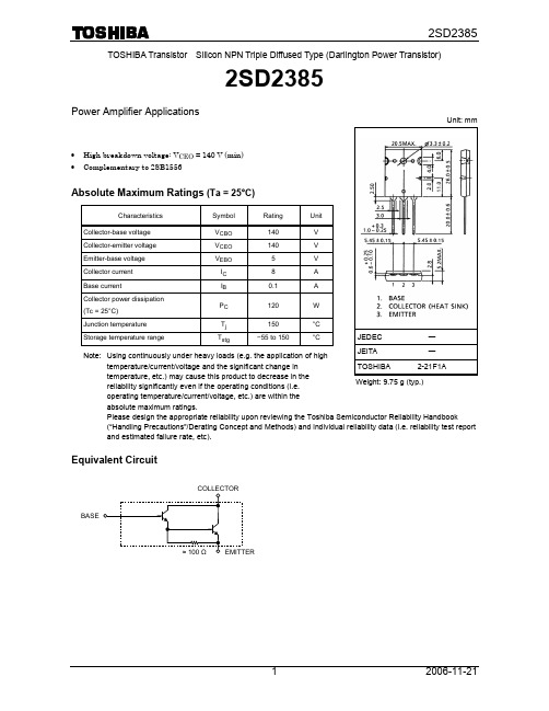
2SD2385资料
• TOSHIBA is continually working to improve the quality and reliability of its products. Nevertheless, semiconductor devices in general can malfunction or fail due to their inherent electrical sensitivity and vulnerability to physical stress. It is the responsibility of the buyer, when utilizing TOSHIBA products, to comply with the standards of safety in making a safe design for the entire system, and to avoid situations in which a malfunction or failure of such TOSHIBA products could cause loss of human life, bodily injury or damage to property. In developing your designs, please ensure that TOSHIBA products are used within specified operating ranges as set forth in the most recent TOSHIBA products specifications. Also, please keep in mind the precautions and conditions set forth in the “Handling Guide for Semiconductor Devices,” or “TOSHIBA Semiconductor Reliability Handbook” etc..
2380中文资料
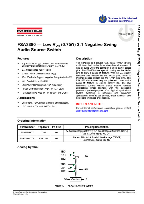
February 2007© 2006 Fairchild Semiconductor CorporationFSA2380 Rev. 1.0.2FSA2380 — Low R ON (0.75Ω) 3:1 Negative Swing Audio Source SwitchClick here for this datasheet translated into Chinese!FSA2380 — Low R ON (0.75Ω) 3:1 Negative Swing Audio Source SwitchFeatures 10µA Maximum I CCT Current Over An Expanded Control Voltage Range (V IN =2.6V, V CC =4.3V) C ON Capacitance 70pF Typical 0.75Ω Typical On Resistance (R ON )1Bn, 2Bn Ports Support Negative Swing Audio to -2V -3db Bandwidth: > 120 MHzLow Power Consumption (1µA maximum) Power-Off Feature for 1A/2A Pin (I IN < 2µA) Packaged in Pb-Free 14-Pin TSSOP and DQFNApplicationsCell Phone, PDA, Digital Camera, and NotebookLCD Monitor, TV, and Set-Top BoxDescriptionThe FSA2380 is a Double-Pole, Triple Throw (DP3T) multiplexer that routes three dual-channel sources of data or audio under the control of a single pair of select pins. The FSA2380 has special circuitry on the 1A/2A pins to allow a power-off feature. With the V CC supply removed and voltage on the 1A/2A pins, there is minimal leakage current into the 1A/2A data pins. The FSA2380 also features very low quiescent current and a power-off feature to extend battery life. The low quiescent current feature allows mobile handset applications direct interface with the baseband processor general-purpose I/Os. Typical applications involve switching in portables and consumer applications, such as cell phones, digital cameras, and notebooks with hubs or controllers.IMPORTANT NOTE:For additional performance information, please contact analogswitch@ .Ordering InformationPart NumberTop MarkPb-FreePacking DescriptionFSA2380BQX 2380 Yes 14-Terminal Depopulated very thin Quad Flat-pack No leads (DQFN)2.5 x3.0mm, JEDEC MO-241FSA2380MTCX FSA2380 Yes14-Lead Thin Shrink Small Outline Package (TSSOP)4.4mm wide, JEDEC MO-153Analog SymbolControl S0S12B02B22A2B11B01B21A1B1Figure 1.FSA2380 Analog Symbol™TinyBoost© 2006 Fairchild Semiconductor Corporation FSA2380 Rev. 1.0.2 13。
TOP222Y中文资料
2
D 7/01
PI-1935-091696
Tab Internally Connected to SOURCE Pin
9W
6W
TOP222Y
25 W
15 W
TOP222P or TOP222G
15 W
10 W
TOP223Y
50 W
30 W
TOP223P or TOP223G
25 W
15 W
TOP224Y
75 W
45 W
TOP224P or TOP224G
30 W
20 W
TOP225Y
100 W
60 W
TOP226Y
Three-terminal Off-line PWM Switch
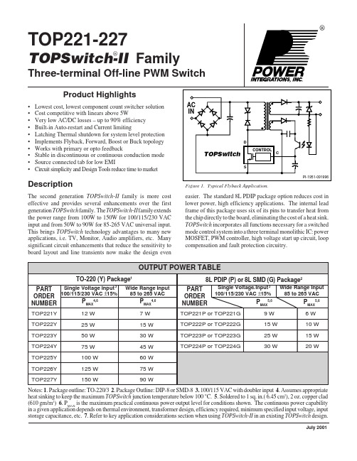
Product Highlights
• Lowest cost, lowest component count switcher solution • Cost competitive with linears above 5W • Very low AC/DC losses – up to 90% efficiency • Built-in Auto-restart and Current limiting • Latching Thermal shutdown for system level protection • Implements Flyback, Forward, Boost or Buck topology • Works with primary or opto feedback • Stable in discontinuous or continuous conduction mode • Source connected tab for low EMI • Circuit simplicity and Design Tools reduce time to market
- 1、下载文档前请自行甄别文档内容的完整性,平台不提供额外的编辑、内容补充、找答案等附加服务。
- 2、"仅部分预览"的文档,不可在线预览部分如存在完整性等问题,可反馈申请退款(可完整预览的文档不适用该条件!)。
- 3、如文档侵犯您的权益,请联系客服反馈,我们会尽快为您处理(人工客服工作时间:9:00-18:30)。
Vishay BCcomponentsHigh Surge Suppression VaristorsThe encapsulation is made of flammable resistant epoxy in accordance with UL94V-0.ORDERING INFORMATIONThe varistors are available in a number of packaging options:•Bulk•On tape on reel•On tape in ammopackThe basic ordering code for each option is given in tables titled Varistors on Tape on Reel, Varistors on Tape in Ammopack and Varistors in Bulk. To complete the catalog number and to determine the required operating parameters, see Electrical Data and Ordering Information table.FEATURES•Zinc oxide disc, epoxy coated•Straight or kinked leads•Component in accordance to RoHS 2002/95/EC and WEEE 2002/96/EC•Certified according to UL1449, VDE/IEC 61051 and CSAAPPLICATION•Supression of transientsDESCRIPTIONThe varistors consist of a disc of low-ß ceramic material with two tinned solid copper leads. They are coated with a layer of ochre coloured epoxy, which provides electrical, mechanical and climatic protection. The encapsulation is resistant to all cleaning solvents in accordance with “IEC 60068-2-45”.MOUNTINGThe varistors are suitable for processing on automatic insertion and cutting and bending equipment.Typical Soldering235 °C, duration: 5 s (Pb-bearing)245 °C, duration: 5 s (Lead (Pb)-free)Resistance to soldering heat260 °C; duration: 10 s max.MARKINGThe varistors are marked with the following information:•Maximum continuous RMS voltage•Series number (582, 583, 584, 585 or 586)•Manufacture logo•Date of manufacture (YYWW)INFLAMMABILITYThe varistors are non-flammable.QUICK REFERENCE DATAPARAMETER VALUE UNIT Maximum continuous voltage:RMS11to680V DC14to895V Maximum non-repetitive transientcurrent I NRP (8 x 20 µs)250 to 10 000A Robustness of terminations10N Drop test:Height of fall1m Detailed specification based onCECC 42000Storage temperature- 40 to + 150°C Operating temperature- 40 to + 125°C RoHS COMPLIANTELECTRICAL DATA AND ORDERING INFORMATIONMAXIMUM CONTINUOUS VOLTAGE VOLTAGE (3)at 1 mAMAXIMUMVOLTAGEat STATEDCURRENTMAXIMUMENERGY (4)(10 X 1000 µS)MAXIMUMNON-REP.TRANSIENTCURRENT (5)I NRP (8 x 20 µs)TYPICALCAPACITANCEat 1 kHzCATALOG NUMBERS (1)RMS (2) (V)DC(V)(V)V(V)I(A)(J)(A)(pF)12 NC (6)SAP (7)11141840 1.00.725016002381 582 x110y VDRH05B011xyE 36 2.5 1.550036002381 583 x110y VDRH07D011xyE 36 5.0 2.6100080002381 584 x110y VDRH10G011xyE 3610.0 5.2200020 0002381 585 x110y VDRH14M011xyE 3620.013.0300040 0002381 586 x110y VDRH20R011ByEHigh Surge Suppression Varistors Vishay BCcomponents14182248 1.00.825013002381 582 x140y VDRH05B014xyE 43 2.5 1.750028002381 583 x140y VDRH07D014xyE 43 5.0 3.2100060002381 584 x140y VDRH10G014xyE 4310.0 6.3200015 0002381 585 x140y VDRH14M014xyE 4320.016.0300030 0002381 586 x140y VDRH20R014ByE1760 1.0 1.125010502381 582 x170y VDRH05B017xyE53 2.5 2.150020002381 583 x170y VDRH07D017xyE 222753 5.0 3.9100040002381 584 x170y VDRH10G017xyE 5310.07.8200010 0002381 585 x170y VDRH14M017xyE5320.019.0300020 0002381 586 x170y VDRH20R017ByE2073 1.0 1.32509002381 582 x200y VDRH05B020xyE65 2.5 2.850015002381 583 x200y VDRH07D020xyE 263365 5.0 4.8100030002381 584 x200y VDRH10G020xyE 6510.09.5200075002381 585 x200y VDRH14M020xyE6520.024.0300015 0002381 586 x200y VDRH20R020ByE2586 1.0 1.52505002381 582 x250y VDRH05B025xyE77 2.5 3.050013502381 583 x250y VDRH07D025xyE 313977 5.0 5.6100026002381 584 x250y VDRH10G025xyE 7710.011.0200065002381 585 x250y VDRH14M025xyE7720.028.0300013 0002381 586 x250y VDRH20R025ByE30104 1.0 1.82507002381 582 x300y VDRH05B030xyE93 2.5 3.850016002381 583 x300y VDRH07D030xyE 384793 5.0 6.8100027002381 584 x300y VDRH10G030xyE 9310.014.0200060002381 585 x300y VDRH14M030xyE9320.034.0300012 0002381 586 x300y VDRH20R030ByE35123 1.0 2.22505602381 582 x350y VDRH05B035xyE110 2.5 4.450013002381 583 x350y VDRH07D035xyE 4556110 5.08.1100022002381 584 x350y VDRH10G035xyE 11010.016.0200048002381 585 x350y VDRH14M035xyE11020.041.0300096002381 586 x350y VDRH20R035ByE40150 1.0 2.62504602381 582 x400y VDRH05B040xyE135 2.5 5.450010002381 583 x400y VDRH07D040xyE 5668135 5.09.8100018002381 584 x400y VDRH10G040xyE 13510.020.0200038002381 585 x400y VDRH14M040xyE13520.049.0300076002381 586 x400y VDRH20R040ByE506582145 5.0 3.58003702381 582 x500y VDRH05E050xyE 13510.07.017509002381 583 x500y VDRH07K050xyE 13525.014.0350015002381 584 x500y VDRH10S050xyE 13550.028.0600031002381 585 x500y VDRH14V050xyE60175 5.0 4.58002902381 582 x600y VDRH05E060xyE16510.09.017507002381 583 x600y VDRH07K060xyE 8510016525.018.0350012002381 584 x600y VDRH10S060xyE 16550.036.0600023002381 585 x600y VDRH14V060xyE165100.072.010 00046002381 586 x600y VDRH20X060ByEELECTRICAL DATA AND ORDERING INFORMATIONMAXIMUM CONTINUOUS VOLTAGE VOLTAGE (3)at 1 mAMAXIMUMVOLTAGEat STATEDCURRENTMAXIMUMENERGY (4)(10 X 1000 µS)MAXIMUMNON-REP.TRANSIENTCURRENT (5)I NRP (8 x 20 µs)TYPICALCAPACITANCEat 1 kHzCATALOG NUMBERS (1)RMS (2) (V)DC(V)(V)V(V)I(A)(J)(A)(pF)12 NC (6)SAP (7)Vishay BCcomponents High Surge Suppression Varistors75210 5.0 5.58002402381 582 x750y VDRH05E075xyE20010.011.017505302381 583 x750y VDRH07K075xyE 10012020025.022.0350010002381 584 x750y VDRH10S075xyE 20050.044.0600019002381 585 x750y VDRH14V075xyE200100.088.010 00038002381 586 x750y VDRH20X075ByE95260 5.0 6.58001802381 582 x950y VDRH05E095xyE25010.013.017504502381 583 x950y VDRH07K095xyE 12515025025.025.0350******** 584 x950y VDRH10S095xyE 25050.053.0600015002381 585 x950y VDRH14V095xyE250100.0106.010 00030002381 586 x950y VDRH20X095ByE115320 5.08.08001502381 582 x111y VDRH05E115xyE30010.016.017503902381 583 x111y VDRH07K115xyE 150********.032.0350******** 584 x111y VDRH10S115xyE 30050.065.0600013202381 585 x111y VDRH14V115xyE300100.0130.010 00026402381 586 x111y VDRH20X115ByE130355 5.08.58001302381 582 x131y VDRH05E130xyE34010.017.517503202381 583 x131y VDRH07K130xyE 17020534025.035.0350******** 584 x131y VDRH10S130xyE 34050.070.0600010502381 585 x131y VDRH14V130xyE340100.0140.010 00021002381 586 x131y VDRH20X130ByE140380 5.09.08001202381 582 x141y VDRH05E140xyE36010.019.017502902381 583 x141y VDRH07K140xyE 180********.039.0350******** 584 x141y VDRH10S140xyE 36050.078.060009502381 585 x141y VDRH14V140xyE360100.0155.010 00019002381 586 x141y VDRH20X140ByE150415 5.010.58001102381 582 x151y VDRH05E150xyE39510.021.017502702381 583 x151y VDRH07K150xyE 20024039525.042.0350******** 584 x151y VDRH10S150xyE 39550.084.060008502381 585 x151y VDRH14V150xyE395100.0168.010 00017002381 586 x151y VDRH20X150ByE175475 5.011.0800902381 582 x171y VDRH05E175xyE45510.024.017502302381 583 x171y VDRH07K175xyE 22527545525.049.0350******** 584 x171y VDRH10S175xyE 45550.099.060007502381 585 x171y VDRH14V175xyE455100.0190.010 00015002381 586 x171y VDRH20X175ByE195525 5.012.0800802381 582 x191y VDRH05E195xyE45510.026.017502102381 583 x191y VDRH07K195xyE 25030045525.052.0350******** 584 x191y VDRH10S195xyE 45550.0105.060006902381 585 x191y VDRH14V195xyE455100.0210.010 00013502381 586 x191y VDRH20X195ByE210575 5.013.0800752381 582 x211y VDRH05E210xyE50510.028.017501902381 583 x211y VDRH07K210xyE 27533050525.058.0350******** 584 x211y VDRH10S210xyE 50550.0115.060006102381 585 x211y VDRH14V210xyE505100.0228.010 00012502381 586 x211y VDRH20X210ByEELECTRICAL DATA AND ORDERING INFORMATIONMAXIMUM CONTINUOUS VOLTAGE VOLTAGE (3)at 1 mAMAXIMUMVOLTAGEat STATEDCURRENTMAXIMUMENERGY (4)(10 X 1000 µS)MAXIMUMNON-REP.TRANSIENTCURRENT (5)I NRP (8 x 20 µs)TYPICALCAPACITANCEat 1 kHzCATALOG NUMBERS (1)RMS (2) (V)DC(V)(V)V(V)I(A)(J)(A)(pF)12 NC (6)SAP (7)High Surge Suppression Varistors Vishay BCcomponents230620 5.016.0800702381 582 x231y VDRH05E230xyE59510.032.017501702381 583 x231y VDRH07K230xyE 30036059525.065.0350******** 584 x231y VDRH10S230xyE 59550.0130.060005402381 585 x231y VDRH14V230xyE595100.0255.010 00011002381 586 x231y VDRH20X230ByE250675 5.017.0800602381 582 x251y VDRH05E250xyE65010.035.017501602381 583 x251y VDRH07K250xyE 32039065025.070.0350******** 584 x251y VDRH10S250xyE 65050.0140.060004802381 585 x251y VDRH14V250xyE650100.0275.010 0009602381 586 x251y VDRH20X250ByE275745 5.020.0800552381 582 x271y VDRH05E275xyE71010.040.017501402381 583 x271y VDRH07K275xyE 35043071025.080.0350******** 584 x271y VDRH10S275xyE 71050.0155.060004402381 585 x271y VDRH14V275xyE710100.0303.010 0009002381 586 x271y VDRH20X275ByE300810 5.021.0800502381 582 x301y VDRH05E300xyE77510.042.017501302381 583 x301y VDRH07K300xyE 38547077525.085.0350******** 584 x301y VDRH10S300xyE 77550.0175.060004002381 585 x301y VDRH14V300xyE775100.0350.010 0008102381 586 x301y VDRH20X300ByE320420510880 5.022.0800452381 582 x321y VDRH05E320xyE 84210.045.017501202381 583 x321y VDRH07K320xyE 84225.092.0350******** 584 x321y VDRH10S320xyE 84250.0190.060003702381 585 x321y VDRH14V320xyE 842100.0382.010 0007502381 586 x321y VDRH20X320ByE350460560940 5.025.0800422381 582 x351y VDRH05E350xyE 92010.051.017501102381 583 x351y VDRH07K350xyE 92025.0102.0350******** 584 x351y VDRH10S350xyE 92050.0205.060003202381 585 x351y VDRH14V350xyE 920100.0410.010 0006502381 586 x351y VDRH20X350ByE3855056201050 5.027.0800402381 582 x381y VDRH05E385xyE 102510.054.01750952381 583 x381y VDRH07K385xyE 102525.0107.0350******** 584 x381y VDRH10S385xyE 102550.0215.060002802381 585 x381y VDRH14V385xyE 1025100.0420.010 0005702381 586 x381y VDRH20X385ByE4205606801150 5.028.0800352381 582 x421y VDRH05E420xyE 112010.056.01750852381 583 x421y VDRH07K420xyE 112025.0112.0350******** 584 x421y VDRH10S420xyE 112050.0225.060002502381 585 x421y VDRH14V420xyE 1120100.0430.010 0005102381 586 x421y VDRH20X420ByE4606157501290 5.029.0800302381 582 x461y VDRH05E460xyE 124010.058.01750752381 583 x461y VDRH07K460xyE 124025.0115.0350******** 584 x461y VDRH10S460xyE 124050.0230.060002252381 585 x461y VDRH14V460xyE 1240100.0440.010 0004502381 586 x461y VDRH20X460ByEELECTRICAL DATA AND ORDERING INFORMATIONMAXIMUM CONTINUOUS VOLTAGE VOLTAGE (3)at 1 mAMAXIMUMVOLTAGEat STATEDCURRENTMAXIMUMENERGY (4)(10 X 1000 µS)MAXIMUMNON-REP.TRANSIENTCURRENT (5)I NRP (8 x 20 µs)TYPICALCAPACITANCEat 1 kHzCATALOG NUMBERS (1)RMS (2) (V)DC(V)(V)V(V)I(A)(J)(A)(pF)12 NC (6)SAP (7)Vishay BCcomponentsHigh Surge Suppression VaristorsNotes(1)The products are certified according to UL (E98144), VDE (40013495) and CSA (219883)(2)The sinusoidal voltage is assumed as the normal operating condition. If a non-sinusoidal voltage is present, type selection should be based on multiplying the peak voltage by a factor of 0.707.(3)The voltage measured at 1 mA meets the requirements of “paragraph 4.3 of CECC specification 42000“.The tolerance on the voltage at 1 mA is ± 10 %.(4)High energy surges are generally of longer duration. The maximum energy for one pulse of 10 x 1000µs is given as a reference for longer duration pulses. This pulse can be characterised by peak current (I p ) and pulse width t 2 (virtual time of half I p value, following “IEC 60060-2,section 6“). If V p is the clamping voltage corresponding to I p , the energy absorbed in the varistor is determined by the formula:where:a) K is dependant on the value of t2 when the value of t1 is between 8 µs and 10 µs; see Peak Current as a Function of Pulse Width drawing (5)A current wave of 8 x 20 µs (requirement of “paragraph B.2.10.1 of CECC specification 42000”) is used as a standard for pulse current and clamping voltage ratings. The maximum non-repetitive transient current is given for one pulse applied during the life of the component.(6)For composition of the 12NC part number replace “x” and “y” by figures from the sections “Varistors in Bulk”, “Varistors on Tape in Ammopack”and “Varistors on “Tape on Reel”(7)For composition of the SAP part number:Replace “x” by B for bulk typeReplace “y” byS for straight leadsT for tape and reelK for kinked leads (bulk only)A for tape and ammopackL for kinked leads with H 0 = 16 mm (tape and reel/ammo)M for kinked leads with H 0 = 18.25 mm (tape and reel/ammo)485640780129010.059.01750652381 583 x481y VDRH07K485xyE 129025.0116.0350******** 584 x481y VDRH10S485xyE 129050.0233.060002202381 585 x481y VDRH14V485xyE 1290100.0450.010 0004002381 586 x481y VDRH20X485ByE 510670820135510.060.01750622381 583 x511y VDRH07K510xyE 135525.0118.0350******** 584 x511y VDRH10S510xyE 135550.0235.060002202381 585 x511y VDRH14V510xyE 1355100.0460.010 0004002381 586 x511y VDRH20X510ByE 550150025.0127.0350******** 584 x551y VDRH10S550xyE 745910150050.0255.060001802381 585 x551y VDRH14V550xyE 1500100.0510.010 0003202381 586 x551y VDRH20X550ByE 625165025.0140.0350******** 584 x6216VDRH10S625ByE 8251000165050.0283.060001652381 585 x6216VDRH14V625ByE 1650100.0566.010 0002802381 586 x6216VDRH20X625ByE 680181525.0155.0350******* 584 x6816VDRH10S680ByE 8951100181550.0310.060001502381 585 x6816VDRH14V680ByE 1815100.0620.010 0002502381 586 x6816VDRH20X680ByEELECTRICAL DATA AND ORDERING INFORMATIONMAXIMUMCONTINUOUSVOLTAGE VOLTAGE (3)at 1 mAMAXIMUMVOLTAGE at STATED CURRENT MAXIMUM ENERGY (4)(10 X 1000 µS )MAXIMUM NON-REP.TRANSIENT CURRENT (5)I NRP (8 x 20 µs)TYPICAL CAPACITANCE at 1 kHz CATALOG NUMBERS (1)RMS (2)(V)DC(V)(V)V (V)I (A)(J)(A)(pF)12 NC (6)SAP (7)E Kx V p x I p x t 2=High Surge Suppression VaristorsVishay BCcomponentsELECTRICAL CHARACTERISTICS DERATING CURVEPEAK CURRENT AS A FUNCTION OF PULSE WIDTHELECTRICAL DATAPARAMETERVALUE UNIT Maximum continuous voltage:RMS 11to 680V DC14to 895V Maximum non-repetitive transient current (I NRP ) (8 x 20 µs):2381582...../VDRH05......E 250 or 800A 2381583...../VDRH07......E 500 or 1750A 2381584...../VDRH10......E 1000 or 3500A 2381585...../VDRH14......E 2000 or 6000A 2381586...../VDRH20......E 3000 or 10 000A Thermal resistance:2381582...../VDRH05......E ≈ 80K/W 2381583...../VDRH07......E ≈ 70K/W 2381584...../VDRH10......E ≈ 60K/W 2381585...../VDRH14......E ≈ 50K/W 2381586...../VDRH20......E ≈ 40K/W Maximum dissipation:2381582...../VDRH05......E 100mW 2381583...../VDRH07......E 250mW 2381584...../VDRH10......E 400mW 2381585...../VDRH14......E 600mW 2381586...../VDRH20......E1000mW T emperature coefficient of voltage at 1mA maximum ± 0.05%/K Voltage proof between interconnected leads and case 2500V Storage temperature - 40 to + 150°C Operating temperature- 40 to + 125°CCOMPONENT DIMENSIONS (BULK TYPE) in millimeters AND CATALOG NUMBERSD NOM.D MAX.A MAX.A 0MAX.L MIN.T MAX.d F CATALOG NUMBER 5.07.09.011.024.070.6± 0.055± 1.02381582...../VDRH05.....E 7.09.011.013.024.070.6± 0.055± 1.02381583...../VDRH07.....E 10.013.515.518.017.0100.8± 0.057.5± 1.02381584...../VDRH10.....E 14.017.019.023.016.0110.8± 0.057.5± 1.02381585...../VDRH14.....E 20.023.025.028.024.0111.0± 0.0510± 1.02381586...../VDRH20.....EVishay BCcomponentsHigh Surge Suppression VaristorsDIMENSIONS in millimeters: see Component Dimensions and Catalog Numbers T ableVARISTORS IN BULKTYPE2381582.....Ø 5mm 11V to 460V2381583.....Ø 7mm 11V to 510V2381584.....Ø 10mm 11V to 680V2381585.....Ø 14mm 11V to 680V2381586.....Ø 20mm 11V to 680VStraight leads; see Outline of components with straight leads drawing5...6 5...6 5...6 5...6 5 (6)Kinked leads; see Outline of components with kinked leads drawing6...6 6...6 6...6 6...6 6 (6)Packing quantities 14 V to 95 V 25025025010050130 V to 385 V 25025025010050420 V to 460 V 25025020010050485 V to max. V-25015010050Outline of component with straight leadsOutline of component with kinked leadsHigh Surge Suppression VaristorsVishay BCcomponentsNote(1)Except for 35 and 40 V = 1000 piecesDIMENSIONS OF AMMOPACK in millimetersVARISTORS ON TAPE IN AMMOPACKTYPE 2381582.....Ø 5 mm 11V to 460V 2381583.....Ø 7mm 11 V to 510V 2381584.....Ø 10mm 11V to 550V 2381585.....Ø 14mm 11 V to 550VStraight leads H = 18 mm --0...70...7H = 20 mm0 (7)0 (7)--See drawing T aped version with straight leads Kinked leads H 0 = 18.25 mm 3...7 3...7 3...7 3...7H 0 = 16 mm8 (7)8 (7)8 (7)8 (7)See drawing T aped version with kinked leads Packing quantities 14V to 210V 1500 (1)1500 (1)500500230V to max.V 10001000500500Vishay BCcomponentsHigh Surge Suppression VaristorsPACKAGINGVARISTORS ON TAPE AND REELTYPE 2381582.....Ø 5mm 11V to 460V2381583.....Ø 7mm 11 V to 510V2381584.....Ø 10mm 11V to 550V2381585.....Ø 14mm 11 V to 550VStraight leads H = 18 mm --0...60...6H = 20 mm0 (6)0 (6)--See drawing T aped version with straight leads Kinked leads H 0 = 18.25 mm 3...6 3...6 3...6 3...6H 0 = 16 mm8 (6)8 (6)8 (6)8 (6)See drawing T aped version with kinked leads Packing quantities 14V to 250 V 150015001000750275V to 300 V 15001500750750320V to 350V 10001000500500385V to max.V10001000500500TAPED VERSION WITH STRAIGHT LEADS (only for 2381 582 ...../VDRH05.....E and 2381 583 ...../VDRH07.....E)TAPED VERSION WITH STRAIGHT LEADS (only for 2381 584 ...../VDRH10.....E and 2381 585 ...../VDRH14.....E)High Surge Suppression VaristorsVishay BCcomponentsDIMENSIONS OF REELS in millimetersTAPED VERSION WITH KINKED LEADS (only for 2381 582 ...../VDRH10.....E and2381 583 ...../VDRH07.....E)TAPED VERSION WITH KINKED LEADS (only for 2381 584 ...../VDRH10.....E and2381 585 ...../VDRH14.....E)For 2381 582 ...../VDRH05.....E and 2381 583 ...../VDRH07.....E For 2381 584 ...../VDRH10.....E and 2381 585 ...../VDRH14.....ETAPING DATA (based on “IEC60286-2”)DIMENSIONS/TOLERANCESYMBOL PARAMETER582583584585A Mounting height9.0 max.11.0 max.15.5 max.19.0 max.A o Mounting height11.0 max.13.0 max.18.0 max.23.0 max.D Body diameter7.0 max.9.0 max.13.5 max.17.0 max. D0Feed hole diameter 4.0 ± 0.2d Lead wire diameter0.6 ± 0.050.8 ± 0.05F Lead to lead distance (1) 5.0 ± 0.5/- 0.27.5 ± 0.8H Distance component to tape center (4)20.0 + 2.0/- 0.018.0 + 2.0/- 0.0H0Lead-wire clinch height16.0 or 18.25 ± 0.5Δh Component alignment0.0 ± 2.0P Component pitch12.7 ± 1.025.4 ± 1.0P0Feed hole pitch (2)12.7 ± 0.3P1Feed hole center to lead center 3.85 ± 0.78.95 ± 0.7Δ p Component alignment0.0 ± 1.3T Total thickness7.0 max.7.0 max.10.0 max.11.0 max. t Total tape thickness (3) 1.7 max.W Tape width18.0 + 1.0/- 0.5W0Hold down tape width10 min.W1Hole position9.0 ± 0.5W2Hold down tape position 3.0 max.Notes(1)Guaranteed between component and tape(2)Cumulative pitch-error ± 1.0 mm to 20 pitches(3)With cardboard tape from 0.5 mm ± 0.1(4)For 2381 585 0511y and 2381 585 0551y: H = 20 ± 0.1 mmV/I CHARACTERISTIC, 11 TO 40 V (RMS); 2381 582 ...../VDRH05.....EV/I CHARACTERISTIC, 50 TO 460 V (RMS); 2381 582 ...../VDRH05.....EV/I CHARACTERISTIC, 11 TO 40 V (RMS); 2381 583 ...../VDRH07.....EV/I CHARACTERISTIC, 50 TO 510 V (RMS); 2381 583 ...../VDRH07.....EV/I CHARACTERISTIC, 11 TO 40 V (RMS); 2381 584 ...../VDRH10.....EV/I CHARACTERISTIC, 50 TO 300 V (RMS); 2381 584 ...../VDRH10.....EV/I CHARACTERISTIC, 320 TO 680 V (RMS); 2381 584 ...../VDRH10.....EV/I CHARACTERISTIC, 11 TO 40 V (RMS); 2381 585 ...../VDRH14.....EV/I CHARACTERISTIC, 50 TO 300 V (RMS); 2381 585 ...../VDRH14.....EV/I CHARACTERISTIC, 300 TO 385 V (RMS); 2381 585 ...../VDRH14.....EV/I CHARACTERISTIC, 11 TO 40 V (RMS); 2381 586 ...../VDRH20.....EV/I CHARACTERISTIC, 50 TO 300 V (RMS); 2381 586 ...../VDRH20.....EV/I CHARACTERISTIC, 320 TO 680 V (RMS); 2381 586 ...../VDRH20.....EMAXIMUM APPLICABLE TRANSIENT CURRENT AS A FUNCTION OF PULSE DURATION,11 V TO 40 V (RMS); 2381 582 ...../VDRH05.....EMAXIMUM APPLICABLE TRANSIENT CURRENT AS A FUNCTION OF PULSE DURATION, 50 V TO 300 V (RMS); 2381 582 ...../VDRH05.....EMAXIMUM APPLICABLE TRANSIENT CURRENT AS A FUNCTION OF PULSE DURATION, 11 V TO 40 V (RMS); 2381 583 ...../VDRH07.....EMAXIMUM APPLICABLE TRANSIENT CURRENT AS A FUNCTION OF PULSE DURATION, 50 V TO 300 V (RMS); 2381 583 ...../VDRH07.....EMAXIMUM APPLICABLE TRANSIENT CURRENT AS A FUNCTION OF PULSE DURATION,11 V TO 40 V (RMS); 2381 584 ...../VDRH10.....EMAXIMUM APPLICABLE TRANSIENT CURRENT AS A FUNCTION OF PULSE DURATION, 50 V TO 300 V (RMS); 2381 584 ...../VDRH10.....EMAXIMUM APPLICABLE TRANSIENT CURRENT AS A FUNCTION OF PULSE DURATION,320 V TO 680 V (RMS); 2381 584 ...../VDRH10.....EMAXIMUM APPLICABLE TRANSIENT CURRENT AS A FUNCTION OF PULSE DURATION,11 V TO 40 V (RMS); 2381 585 ...../VDRH14.....EMAXIMUM APPLICABLE TRANSIENT CURRENT AS A FUNCTION OF PULSE DURATION, 50 V TO 300 V (RMS); 2381 585 ...../VDRH14.....EMAXIMUM APPLICABLE TRANSIENT CURRENT AS A FUNCTION OF PULSE DURATION,320 V TO 680 V (RMS); 2381 585 ...../VDRH14.....EMAXIMUM APPLICABLE TRANSIENT CURRENT AS A FUNCTION OF PULSE DURATION,11 V TO 40 V (RMS); 2381 586 ...../VDRH20.....EMAXIMUM APPLICABLE TRANSIENT CURRENT AS A FUNCTION OF PULSE DURATION, 50 V TO 300 V (RMS); 2381 586 ...../VDRH20.....E320 V TO 680 V (RMS); 2381 586 ...../VDRH20.....EDocument Number: 91000 Revision: 18-Jul-081DisclaimerLegal Disclaimer NoticeVishayAll product specifications and data are subject to change without notice.Vishay Intertechnology, Inc., its affiliates, agents, and employees, and all persons acting on its or their behalf (collectively, “Vishay”), disclaim any and all liability for any errors, inaccuracies or incompleteness contained herein or in any other disclosure relating to any product.Vishay disclaims any and all liability arising out of the use or application of any product described herein or of any information provided herein to the maximum extent permitted by law. The product specifications do not expand or otherwise modify Vishay’s terms and conditions of purchase, including but not limited to the warranty expressed therein, which apply to these products.No license, express or implied, by estoppel or otherwise, to any intellectual property rights is granted by this document or by any conduct of Vishay.The products shown herein are not designed for use in medical, life-saving, or life-sustaining applications unless otherwise expressly indicated. Customers using or selling Vishay products not expressly indicated for use in such applications do so entirely at their own risk and agree to fully indemnify Vishay for any damages arising or resulting from such use or sale. Please contact authorized Vishay personnel to obtain written terms and conditions regarding products designed for such applications.Product names and markings noted herein may be trademarks of their respective owners.元器件交易网。
