NCP361过压保护控制器
基于USB3.0高速图像数据传输系统设计

基于USB3.0高速图像数据传输系统设计王国忠;刘磊;储成群;任勇峰;焦新泉【摘要】为了解决图像采集系统中实时数据的高速缓存与传输问题,提出了一种基于高数据带宽、大容量的DDR2 SDRAM存储器和支持突发传输的USB3.0数据传输接口的设计方案.在硬件设计中,采用CYUSB3014作为USB3.0的控制芯片实现FPGA与上位机之间高速图像数据传输,以及采用DDR2 SDRAM作为缓存器;在逻辑设计中采用手动DMA模式对数据流进行控制,避免数据的堵塞,提高了可靠性.经验证,该系统工作稳定,能有效解决海量图像数据的缓存与传输问题.【期刊名称】《仪表技术与传感器》【年(卷),期】2019(000)003【总页数】5页(P106-109,113)【关键词】高速缓存;DDR2SDRAM;USB3.0;手动DMA;可靠性【作者】王国忠;刘磊;储成群;任勇峰;焦新泉【作者单位】中北大学,电子测试技术国家重点实验室,山西太原 030051;中北大学,电子测试技术国家重点实验室,山西太原 030051;中北大学,电子测试技术国家重点实验室,山西太原 030051;中北大学,电子测试技术国家重点实验室,山西太原030051;中北大学,电子测试技术国家重点实验室,山西太原 030051【正文语种】中文【中图分类】TP2740 引言随着大数据智能化时代的到来,以及工业4.0的提出,智能化系统对图像分辨率的要求越来越高,即图像采集系统需要传输的数据量越来越大。
数据传输的速度和缓冲区的大小是图像采集系统中非常重要的一部分,如果缓冲的速度与传输的速度不匹配的话,就会使数据丢失或者堵塞,因此需要对整个系统进行综合设计。
1 总体方案设计系统总体方案设计如图1所示,由图像采集模块、数据处理模块、数据传输模块3部分组成。
图像采集模块采集模拟数据,并转化为数字图像数据传输给数据处理模块;数据处理模块接收图像数据,经处理后转存到缓冲芯片DDR2 SDRAM中,同时接收上位机下发命令,把数据实时上传;数据传输模块把数据上传到上位机软件进行图像显示,并负责上位机与FPGA之间的通信。
NCPS产品选型介绍及问题处理

NCPS产品介绍选型及问题处理一、产品介绍1、产品功能:分为控制与保护两部分;①控制:指的是产品可以就地控制或者远程控制;就地控制:就是手柄直接去旋转,比如老彩电直接按电视上的电源键启动;远程控制:就是按门板上的按钮,比如电视上的遥控器操作。
②保护:电流及电压保护电流保护:类似断路器,当产品有过故障时提供跳闸保护;A、过载:反曲线保护,过载越多,跳闸也越快(1.5倍电流47秒保护);B、三相电流不平衡:提供保护,极端情况缺相,也提供保护。
电压保护:过压和欠压保护过压:220V*1.15=254V,现场电压超过254V,起过压保护;欠压:220V*0.85=187V,现场电压低于187V,起欠压保护。
★漏电型的NCPS,增加零序互感器,采集回路的电流矢量和,矢量和为零时,则无漏电情况。
二、型号介绍NCPS-45/M32/06M(F)(G)(L)NCPS 指企业、产品名称及产品代号45 框架电流M 基本通用32 额定电流06 3常开3常闭辅助触点M 控制电压220V基本通用F 过载只报警不跳闸G 隔离(勿动作)L 漏电检测三、产品选型四、常见问题处理关于NCPS跳闸的解决方法查询故障和解决故障1、启动CPS,按数据键查询故障代码2、参考数码管两侧的错误代码符号查询并解决故障3、相应的故障解决后,再次启动即可线路板电流调节1、按设置键出现电流界面2、配合使用数据键和移位键重新整定电流3、复位键保存即可关闭三相保护功能1、产品空载的情况下按设置键多次,直至出现P50或者P602、数据键和移位键配合使用,改成P00或者POFF3、复位键保存即可基本/消防切换调节方案方案一:1、多次按保存键直至出现n16(如果是45的线路板,则出现n45)2、按查询键多次,直到出现反FOFF(基本型)/FON(消防型)3、按保存键一次,进入修改状态(此时OFF/ON闪烁),再按查询键一次,出现反FON(消防型)/FOFF(基本型)4、按查询键保存(此时ON/OFF不闪烁)。
DMP-361系列备自投说明书--曲阜华能
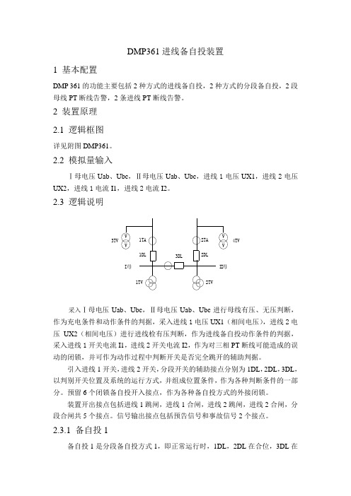
DMP361进线备自投装置1 基本配置DMP 361的功能主要包括2种方式的进线备自投,2种方式的分段备自投,2段母线PT断线告警,2条进线PT断线告警。
2 装置原理2.1 逻辑框图详见附图DMP361。
2.2 模拟量输入Ⅰ母电压Uab、Ubc,Ⅱ母电压Uab、Ubc,进线1电压UX1,进线2电压UX2,进线1电流I1,进线2电流I2。
2.3 逻辑说明采入Ⅰ母电压Uab、Ubc,Ⅱ母电压Uab、Ubc进行母线有压、无压判断,作为充电条件和动作条件的判据,采入进线1电压UX1(相间电压),进线2电压UX2(相间电压)进行进线检有压判断,作为进线备自投动作条件的判据,采入进线1开关电流I1,进线2开关电流I2,作为对三相PT断线可能造成的误动的闭锁,并可作为动作过程中判断开关是否完全跳开的辅助判据。
引入进线1开关,进线2开关,分段开关的辅助接点分别为1DL,2DL,3DL,以判别开关位置及系统的运行方式,并组成位置条件,作为各种判断条件的一部分。
预留6个闭锁备自投开入接点,作为各种备自投方式的外接闭锁。
装置开出接点包括进线1跳闸,进线1合闸,进线2跳闸,进线2合闸,分段合闸共5个接点。
信号输出接点包括预告信号和事故信号2个接点。
2.3.1 备自投1备自投1是分段备自投方式1,即正常运行时,1DL,2DL在合位,3DL在分位,当因故障Ⅱ母失压后,备自投1动作跳开2DL,合3DL。
充电条件:(以下条件应全部满足)1DL,2DL合位,3DL分位;Ⅰ母三相有压,Ⅱ母三相有压;动作条件:(以下条件应全部满足)2DL合位(该条件作为手跳及保护跳闭锁);Ⅰ母三相有压,Ⅱ母三相无压及无流;放电条件:(满足以下任一条件)1、1DL分位,2、2DL分位,3、3DL合位,4、PT断线。
动作过程:跳开2DL,判断2DL跳开后,合3DL。
2.3.2 备自投2备自投2是分段备自投方式2,即正常运行时,1DL,2DL在合位,3DL在分位,当因故障Ⅰ母失压后,备自投2动作跳开1DL,合3DL。
过压保护电路原理

过压保护电路原理
过压保护电路是一种常用的电子保护装置,用于防止电路或电器设备受到过电压的损坏。
其工作原理是通过监测电路中的电压来判断电压是否超过了设定的安全范围,一旦检测到过压情况,就会采取相应的措施来保护电路或设备。
过压保护电路通常由以下几个主要组成部分构成:
1. 电压检测器:通过采集电路中的电压信号来实时监测电压的变化情况。
电压检测器通常采用电阻、电容、二极管等元件构成的电路来完成。
2. 比较器:将电压检测器采集到的电压信号与设定的安全阈值进行比较,判断是否发生了过压。
比较器可以是模拟或数字电路,其功能是判断输入信号是否超过了设定的阈值。
3. 控制器:一旦过压被检测到,控制器会向保护电路发送信号,触发相应的保护措施。
控制器可以是逻辑门电路、微处理器或专用的保护芯片。
4. 保护措施:过压被检测到后,保护措施会被激活以保护电路或设备。
常见的保护措施包括切断电源、短路电流、引入电阻、电容等,以消耗过多的电压或将其分流。
过压保护电路的工作原理是通过不断监测电路中的电压,并判断是否超过设定的阈值,一旦超过阈值,则触发保护措施以防
止电路或设备的损坏。
这种电路广泛应用于各种电子设备和电路中,保护电子器件免受过电压的损坏。
ncp1246工作原理

ncp1246工作原理NCP1246 的工作原理NCP1246 是一种高效率固定频率电流模式降压型 DC-DC 转换器。
它采用高集成度设计,内部集成了所有必需的组件,包括功率MOSFET、振荡器、错误放大器和电流感测电路。
这种紧凑的设计使其非常适合空间受限的应用。
启动和初始化当为 NCP1246 供电时,它会经历一个启动过程。
在此过程中,它会对内部电路进行初始化并进行软启动,以防止系统中的浪涌电流。
1. 上电复位:当为 IC 供电时,内部上电复位电路会将所有寄存器复位为默认值。
2. 软启动:上电后,NCP1246 会逐渐增加其输出电压,以防止系统中的浪涌电流。
这通过一个内部软启动电容来实现,该电容限制了错误放大器的输出电流。
3. 环路补偿:NCP1246 集成了一个内部环路补偿网络,以确保输出电压稳定。
该网络有助于补偿电源电路的极点和零点,从而改善瞬态响应和稳定性。
电流模式控制NCP1246 使用电流模式控制来调节其输出电压。
这种控制方式基于测量流过电感的电流。
1. 电流感测:NCP1246 通过一个检测电阻感测流过电感的电流。
该电流与输出电压的误差信号一起反馈到错误放大器。
2. 错误放大器:NCP1246 的错误放大器比较内部参考电压和输出电压的误差信号。
该误差由外部电压分压器设置。
3. PWM 比较器:错误放大器的输出与一个锯齿波比较器进行比较,该比较器生成一个脉宽调制 (PWM) 信号。
当错误信号大于锯齿波时,功率 MOSFET 导通;当错误信号小于锯齿波时,功率 MOSFET 关断。
输出电压调节NCP1246 通过调节 PWM 信号的占空比来调节其输出电压。
当输出电压下降时,错误放大器中的误差信号增加,导致 PWM 信号的占空比增加。
这会增加流过电感的电流,从而提高输出电压。
相反,当输出电压升高时,误差信号减小,PWM 信号的占空比减小,从而降低输出电压。
保护功能NCP1246 具有多种保护功能,以确保其安全可靠地运行:1. 过流保护:当流过功率 MOSFET 的电流超过预设阈值时,NCP1246 会进入过流保护模式。
消弧及过电压保护装置控制器说明书

消弧及过电压保护装置控制器说明书安徽凯民电力技术有限公司单位名称:安徽凯民电力技术有限公司地址:安徽省合肥市高新区科学大道102号邮编:230088TEL:(0551)5312386FAX:(0551)5322512一、概述在我国3~35KV供电系统中,大部分为中性点不接地系统,这种系统在发生单相接地时,电网仍可带故障运行,这就大大降低了运行成本,提高了供电系统的可靠性,但这种供电方式在单相接地时容易产生弧光接地从而可能引发相间短路,给供电设备造成了极大的危害。
以前的解决办法是在中性点加装消弧线圈补偿电容电流来抑制故障点弧光发生的机率。
很显然,这种方法的目的是为了消除弧光,但由于消弧线圈的自身的诸多特点,很难对电容电流进行有效补偿,特别是高频分量部分对供电设备造成的危害无法克服。
安徽鸿宇电气技术有限公司在研究各种消弧线圈的基础上,提出全新的概念,研制出了智能快速消弧过电压保护装置,该装置在系统出现弧光接地时,通过可以分相控制的真空接触器,使故障相接地,达到彻底消除弧光的目的。
消弧及过电压保护装置控制器,是针对智能快速消弧过电压保护装置研制的一种智能型控制器。
该控制器通过P T互感器检测出故障相,然后发出控制信号命令故障相的接地真空接触器闭合,使弧光接地变成金属性接地。
一、功能及特点1、本控制器结构紧凑,技术先进。
控制器的核心采用Mic roc hip公司生产的PIC单片机和一些外围器件构成信号采集、数据处理系统。
2、根据信号采集、数据处理结果,发出相应的信号。
PT断线、金属性接地,只报警而不接地;当系统出现弧光接地时,微机综合控制器作出判断同时发出动作信号,让接触器动作,使系统对应相转变为金属性接地。
3、可以查询最近18次的历史故障记录。
4、控制器具有485通讯口,上位机可以通过此接口对微机综合控制器进行访问,微机综合控制器给出应答信号,告诉计算机此刻消弧及过电压保护装置的运行状态。
上位机也可以对微综合控制器发出指令。
PMC-851X综合保护测控装置用户说明书_V1.5_131014
手机充电标准

中国信息产业部发布的“YD/T 1591-2006移动通信手持机充电器及接口技术要求和测试方法”标准已经强制执行,预计这一举措将大幅减少中国每年与新手机一起销售的电池充电器的数量,从而降低手机总体材料成本,并减少废弃电子装置带来的环境污染。
YD/T 1591标准涉及两大部分,分别是移动通信手持机侧(简称“手机侧”)和充电器侧。
手机侧指的是手机加上手机连接充电器直流输出端的线缆及其插头,由手机制造商提供;充电器侧指充电器及直流输出连接插座,由充电器厂商提供。
YD/T 1591标准手机侧的要求主要分为三个部分,分别是手机侧连接接口电气性能要求(标准4.2.3.1)、手机侧充电连接接口及线缆要求(标准 4.2.3.3、4.2.3.4)和手机侧供电装置识别(标准4.2.3.5)。
本文将重点结合手机侧的要求来分析USB充电和过压保护设计策略,以及相应的解决方案。
图 1:YD/T 1591-2006 标准所涵盖手机侧和充电器侧两大部分。
手机充电要求及不同充电电路解决方案比较通常所称的手机充电器实际上是交流/直流(AC-DC)电源适配器,真正的充电电路乃是在手机内部。
根据YD/T 1591标准要求,手机充电接口直流输入电压也就是充电器的输出电压为5 V±5%,即范围为4.75 V~5.25 V;标准充电器的充电电流为300 mA至1,800 mA,非标准充电器(如笔记本电脑的USB端口等)的最大充电电流为500 mA。
无论充电器的输出功率如何,手持机侧充电控制电路应能根据自身需求实施安全充电,不应出现过热、燃烧、爆炸以及其它电路损坏的现象。
在手机内部的充电电路方面,业界有着不同的解决方案,主要包括分立式充电IC、集成式充电IC、电源管理集成电路(PMIC,或称电源管理单元,简称 PMU)+外部充电功率元件等三种。
这三种方案各有其特点。
其中,对于分立式充电IC方案而言,优点在于便于增加或修改功能,从而更有利于实现产品差异化,此外,这种方案有利于实现困难的电路板布局,达到苛刻的电磁兼容要求,也具有更好的散热特性。
PCS-9616D_X_说明书_国内中文_国内标准版_X_R1.30
外部回路 当把装置输出的接点连接到外部回路时,须仔细检查所用的外部电源电压,以防止所连接的回
路过热。 连接电缆
仔细处理连接的电缆避免施加过大的外力。
版权声明 © 2015 NR. 南京南瑞继保电气有限公司版权所有
警告!
为增强或修改现有功能,装置的软硬件均可能升级,请确认此版本使用手册和您购买的产品相 兼容。
警告!
电气设备在运行时,这些装置的某些部件可能带有高压。不正确的操作可能导致严重的人身伤 害或设备损坏。
只有具备资质的合格专业工作人员才允许对装置或在装置临近工作。工作人员需熟知本手册中 所提到的注意事项和工作流程,以及安全规定。
1.1 应用范围 ............................................................................................................................. 1 1.2 功能配置 ............................................................................................................................. 1 1.3 性能特征 ............................................................................................................................. 2 1.4 订货须知 ............................................................................................................................. 3 1.5 产品执行标准...................................................................................................................... 3 第 2 章 技术参数 .............................................................................................................................. 5 2.1 电气参数 ............................................................................................................................. 5 2.2 机械结构 ............................................................................................................................. 6 2.3 环境条件参数...................................................................................................................... 7 2.4 通信端口 ............................................................................................................................. 7 2.5 型式试验 ............................................................................................................................. 8 2.6 认证 .................................................................................................................................... 8 2.7 保护功能 ............................................................................................................................. 9 2.8 管理功能 ............................................................................................................................. 9 第 3 章 工作原理 .............................................................................................................................11 3.1 概述 ...................................................................................................................................11 3.2 装置启动元件.....................................................................................................................11 3.3 (短充)过流保护和零序保护 .......................................................................................... 12 3.4 (长充)过流保护和零序保护 .......................................................................................... 13 3.5 同期功能(可选) ............................................................................................................ 14 3.6 异常告警 ........................................................................................................................... 15 3.7 采样数据异常的处理......................................................................................................... 16 3.8 遥控、遥测、遥信功能 ..................................................................................................... 16 3.9 时间管理 ........................................................................................................................... 16 第 4 章 硬件描述 ............................................................................................................................ 19
智浦36v控制器说明书
智浦36v控制器说明书
一、调速功能
控制器与转把相互结合,实现了电机转动快慢。
二、制动断电
通过刹把制动,断电线则传输制动信号,控制器根据信号停止对电机输出电压。
三、欠压保护
行驶中,电池放电到最低时,控制器会对电池进行欠压保护,如果继续行驶,则会损伤电池。
一般一节12V的电池欠压保护是10.5V,所以36V欠压保护值是31,5V48V保护欠压是42V。
四、过流保护
使用过程中,电池的电流超出会造成控制器烧坏或者是电机电子元件损坏,而设计这个功能主要目的是对电机和控制器进行各保护!
五、限速
现在的电动车设计的速度越来越快,一般都有三挡调速按键,低速25码中速40码高速60码。
六、时速显示
通过仪表显示当时电动车行驶的速度。
七、零启动功能
就是在停止状态下,直接转动转把可以原地起步,所以使用比
较广泛。
一种过压过流保护电路[实用新型专利]
![一种过压过流保护电路[实用新型专利]](https://img.taocdn.com/s3/m/a5162df0227916888586d7bc.png)
专利名称:一种过压过流保护电路专利类型:实用新型专利
发明人:沈朝阳
申请号:CN201520746313.1
申请日:20150924
公开号:CN205104900U
公开日:
20160323
专利内容由知识产权出版社提供
摘要:本实用新型公开了一种过压过流保护电路,所述保护电路包括复合型PTC热敏电阻器电路、整流桥电路,复合型PTC热敏电阻器电路的输出端与整流桥电路的输入端连接。
本实用新型通过在复合型PTC热敏电阻器电路中并接整流桥电路,经整流桥电路隔离后提供无限并联的方式提升额定电流;通过复合型PTC热敏电阻中低压敏电压为后级电路提供低的残压保护;通过整流桥的隔离作用,使过压过程中流过压敏电阻的电流只与各自相耦合的PTC热敏电阻相关,正常工作时,流过复合型PTC热敏电阻的电流通过整流桥隔离后在整流桥输出端汇聚在一起为后级负载提供电流。
申请人:湖南劲阳电子有限公司
地址:414005 湖南省岳阳市君山区柳林洲镇富康路
国籍:CN
代理机构:广州市越秀区哲力专利商标事务所(普通合伙)
更多信息请下载全文后查看。
ncp1096工作原理

ncp1096工作原理ncp1096 是一种高效的直流/直流(DC/DC)转换器芯片,适用于电动车电池包、工业设备、通信基站和太阳能发电系统等应用。
它采用先进的开关电源技术,通过将电源输入电压转换为所需的输出电压来完成能量转换。
首先是输入电源的处理。
ncp1096 通过内置的输入电流传感器测量输入电流,并与输入电压比较,以实现功率因数校正(PFC)和电源输入电流限制。
PFC 可以提高系统的能源利用率,减少功率损耗,并提供稳定的输入电压。
输入电流限制则可以防止过流和短路等故障,保护电路安全运行。
接下来是开关控制。
ncp1096 采用了一种称为强插低通滤波(Flyback)的拓扑结构,它包含了两个主要的开关器件,分别是主开关和同步整流器。
主开关负责断开和接通输入电源,而同步整流器则用来降低能量损耗。
这两个开关器件通过一系列的电感和电容连接在一起,形成一个完整的回路。
通过控制开关的开关周期和占空比,可以实现对输入电源的能量转换和电压输出。
最后是输出电压控制。
ncp1096 通过一对误差放大器来监测输出电压,其中一个误差放大器用于电压反馈控制,另一个用于电流反馈控制。
电压反馈控制器通过比较输出电压与参考电压之间的差异,来调节开关的开关周期和占空比,以使输出电压保持在设定值。
电流反馈控制器则用于调节输出电流,并保护电路免受过流和短路等故障的影响。
除了以上基本的工作原理外,ncp1096 还具有一些附加功能,例如过温保护、过压保护和欠压保护。
这些保护机制可以确保电路在异常情况下自动停止运行,并保护相关设备的安全性和稳定性。
总结来说,ncp1096 的工作原理是通过输入电源处理、开关控制和输出电压控制三个步骤来实现电源能量的转换和电压输出。
它具有高效、可靠和稳定的特点,适用于多种应用场合。
STS 361J数字式低周低压解列装置 说明书

六、原理接线图
注:可选用母线电压和线路电压互为 闭锁判据,也可任选一侧
STS 361J
七、逻辑框图
信号回路接点断弧容量 60VA
2.2.3 跳合闸电流
本装置跳合闸电流采用自适应模式,无需选择。
2.2.4 各类元件定值精度
电流元件:
<±5%
电压元件: 时间元件:
<±5% 0s-1s 时,误差不超过 40ms; 1s 以上时,误差不超过<±2.5%;
频率偏差:
<±0.02Hz
滑差定值:
<±5%
2.2.5 整组动作时间(包括继电器固有时间)
STS 361J 数字式低周低压解列装置
一、概述
STS361J 数字式低周低压解列装置适用于 变电站有小电源情况下的低压解列及零序过压 解列功能电厂的低压、低周解列功能。
具体配置见右图。
二、技术参数
2.1 额定参数
2.1.1 额定直流电压: 2.1.2 额定交流数据:
220V 或 110V(订货注明)
出口5-2
7-2
出口8-1 公共端(保持) 呼唤告警信号 保护动作信号 公共端 呼唤告警信号 保护动作信号
标记 处数 更改文件号 签字
日期
设计
标准化
校核
批准
工艺
日期
上海天正明日电力自动化有限公司
STS361J数字式低周低压解列装置
重量 第1页
比例 共1页
背板端子图 STS361J
装置实时计算并进行二段零序过压判别。 装置在执行二段零序过压判别时,各段判别逻辑一致,其动作条件如下:
1) 3U0>U0n ; I0n: 零序过压 N 段定值 2) T>T0n ;T0n: 零序过压 N 段延时定值
什么是浪涌保护器防雷过压保护

什么是浪涌保护器防雷过压保护每年有数十万起雷击和过电压造成的损坏,造成的损失高达数千万元。
过压保护装置是电气装置综合保护概念的一部分,可以可靠地防止过压造成的损坏。
过电压损坏过电压是小于千分之一秒的短暂电压峰值,超过电气设备允许的设计工作电压的许多倍。
此类过电压事件通常是由雷击、静电放电或电网切换操作引起的,并且非常危险。
三级保护应根据安装现场的用电负荷选择保护装置。
这个概念可以实施适合当地条件和个人要求的过电压和雷电保护措施。
满足任何要求的正确设备区分过压保护装置的其他特性包括其额定浪涌容量和可实现的保护水平。
1型避雷器:防止由直接或间接雷击触发的过电压和大电流2型避雷器:防止由电气开关操作触发的过电压3类浪涌保护装置:保护电气负载免受过压过压保护当系统中的电压超过其额定电压时,称为过电压。
这种过电压可能是瞬时的或持续的。
电力系统中产生过电压的主要原因可以方便地分为两类,即内部和外部。
内部过电压源于系统本身,而外部过电压是由于线路上的雷电造成的。
电压浪涌定义:电压浪涌的定义是过电压的突然上升,它会损坏安装的电气设备。
线路中的过电压是由于两相之间以及相与地之间的电压升高而发生的。
电压浪涌的类型电站中的过电压可能由内部干扰或大气喷发引起。
根据过电压的产生,电压浪涌分为两类。
内部过压当系统中的电压超过额定电压时,这种电压称为内部过电压。
外部过电压由大气放电(如静电放电或雷击)引起的过电压称为外部过电压。
工业自动化控制柜中的过电压保护装置工业控制柜控制的自动化设施依赖于这些机柜中的组件,即使在功率变化的情况下也能可靠地工作。
这些组件包括本地电源、P1C、数据记录器、网络和其他通信设备以及IO-—它们都容易受到电压浪涌的不利影响。
过压保护装置过电压(在系统中)一相导体和大地之间或相导体之间的任何电压,其峰值超过国际电工词汇(IEV604-03-09)中设备定义的最高电压的相应峰值。
对电气装置的影响雷电尤其会损坏电气和电子系统:住宅和工业场所中的变压器,电表和电器。
过压保护器的原理
过压保护器的原理过压保护器的原理由于真空开关的灭弧能力极强,开断时会引起特殊的操作过电压,造成高压电机绝缘击穿,回路变压器故障,甚至导致开关柜自身损坏烧毁。
三相组合式过电压保护器(以下简称保护器)是专用于3~35kV中压系统,保护系统内部操作过电压(主要是真空开关强制截流过电压,也包扩多次重燃过电压和三相开断不同步产生的过电压)对电气设备侵害的产品。
其核心工作原理是采用放电间隙给氧化锌阀片分压的方式,降低产品的操作冲击保护残压,实现对操作过电压的保护;同时采用四星型接法(俗称三叉戟式接法),设置公共中性点,实现对相间过电压的快速响应,有效防止三相负载出现相间绝缘击穿。
由于保护器其主要工作元件是氧化锌阀片,与避雷器类似,所以有些地方也将其称为组合式避雷器。
但是,事实上两者的作用是完全不同的。
避雷器以防雷为主要目的;而保护器虽然也可以用于防雷,但主要是与真空开关配套使用,防止操作过电压侵害的。
本系列产品可有效限制大气过电压及各种真空断路器引起的操作过电压,对相间和相对地的过电压均能起到可靠的限制作用,广泛应用于电力、冶金、石化、矿山、建筑、环保等领域的电气设备保护。
本系列保护器设计思路独特新颖,技术性能合理可靠,参数选取科学,极大地提高了产品的保护性能和抗干扰、抗电蚀、耐老化能力。
本系列保护器全面采用新国标技术标准,已通过国家绝缘子避雷器质量监督检验中心的全面型式试验。
二、工作原理和接线方式三相组合式带串联间隙过电压保护器主要由ZnO阀片和三棱体式组合间隙等组成,采用硅橡胶复合外套整体模压一次成形,引出线采用硅橡胶高压电缆,安装时,只需将标有接地符号单元的电缆接地外,其余分别接A、B、C三相即可。
标准电缆长度600mm。
三、性能和特点●相间保护特性与相对地保护特性相同,可把各种过电压限制在设备绝缘允许的范围内。
●采用氧化锌非线性电阻和放电间隙相结合的结构,使两者互为保护,延长产品的寿命。
●采用了三棱体式间隙结构,将放电间隙的数量降到1,从而降低了分布电容和杂散电容对放电数值的影响,相间过电压和相地过电压过程均由一个间隙完成。
高电压过压保护控制器
高电压过压保护控制器
佚名
【期刊名称】《电子技术应用》
【年(卷),期】2008(34)1
【摘要】Maxim推出MAX4959/MAX4960过压保护(OVP)控制器,内置电池切换功能。
该系列器件提供电阻可编程过压(6V-28V)和欠压(5V-28V)门限,专门设计为低压系统提供高达28V的保护。
当输入电压超过过压门限时,MAX4959/MAX4960关断外部pFET,实现OVP并防止损坏受保护的元件。
随后,器件保持外部pFET处于关断状态,直至输入电压超过欠压锁定(UVLO)门限。
【总页数】1页(P13-13)
【关键词】保护控制器;过压保护;高电压;输入电压;欠压锁定;Maxim;切换功能;内置电池
【正文语种】中文
【中图分类】TN86;TM762.1
【相关文献】
1.康佳彩电+B电压过压保护起控点质疑 [J], 石宝岩
2.高应力下卸压巷道围岩破坏机理及卸压过程数值分析 [J], 张伟杰;兰思栋
3.康佳彩电+B电压过压保护“起控点”的实验测试及其调整方法 [J], 刘国江
4.电压小母线意外失压情况下110KV低电压过电流保护动作跳闸原因分析 [J], 张
长梅
5.超诚电子研究所——欠压过压保护模块 [J], 无
因版权原因,仅展示原文概要,查看原文内容请购买。
安徽赛普过电压保护器说明书

安徽赛普过电压保护器说明书引言:过电压保护器是一种用于保护电气设备和电路免受过电压损害的装置。
安徽赛普公司研发的过电压保护器具有高性能和可靠性,能有效保护各种电气设备免受过电压的侵害。
本说明书将详细介绍安徽赛普过电压保护器的特点、原理、安装和使用方法,帮助用户正确使用该设备。
一、产品特点1.1 高性能保护:安徽赛普过电压保护器采用先进的电路设计和高质量的元器件,能够快速响应并有效地保护设备免受过电压的损害。
1.2 安全可靠:该保护器具有过载保护、短路保护等多重保护功能,能够确保设备在过电压情况下安全可靠地工作。
1.3 超长寿命:采用高品质材料和精密制造工艺,保证了过电压保护器的使用寿命长达数十年。
1.4 自动恢复:当过电压保护器触发保护时,它会自动恢复正常工作状态,无需手动干预。
1.5 多种型号可选:根据不同电气设备的需求,安徽赛普过电压保护器提供了多种型号和额定电压等级可供选择。
二、工作原理安徽赛普过电压保护器基于电气设备通电过程中产生的过电压现象,通过监测电压信号的变化,及时触发保护装置,以保护设备免受过电压的伤害。
其工作原理如下:2.1 过电压监测:过电压保护器内置感应电路,能够实时监测电气设备的电压变化。
2.2 触发保护:当电压超过设定的安全范围时,过电压保护器会触发保护装置,切断电气设备与电源的连接,防止过电压对设备造成损害。
2.3 自动恢复:一旦过电压保护器触发保护,它会自动恢复正常工作状态,保证设备正常运行。
三、安装方法3.1 准备工作:在安装过电压保护器之前,首先需要确保电气设备与电源已经断电,并检查保护器是否完好无损。
3.2 安装位置:过电压保护器应安装在电气设备的供电线路上,通常选择在电源进线处或设备的控制柜中安装。
3.3 接线方法:根据过电压保护器的接线图,将保护器与电气设备的电源线路进行连接。
确保接线牢固可靠,并遵循电气安全规范。
3.4 安全接地:为了确保过电压保护器的稳定性和可靠性,应将保护器的接地线连接到设备的接地系统。
110v电源端过压保护电路

110v电源端过压保护电路
110V电源端过压保护电路主要包括电源过压保护器和过压保护电路两部分。
电源过压保护器是一种用来检测整个电网的电压是否超过设定的阈值,并在超过时切断电源供应的设备。
它主要由电压监测电路、比较器和控制开关组成。
当电源电压超过阈值时,电压监测电路会检测到这一情况,并通过比较器将信号送入控制开关,切断电源供应,防止过压对电器设备造成损坏。
过压保护电路用于保护特定电器设备不受电源过压的影响。
它主要包括电压调节器、过压保护瞬断器和故障指示电路。
电压调节器用来将电源电压稳定在合适的范围内,避免电压过高。
过压保护瞬断器用来在电压超过设定阈值时瞬间切断电路,以保护电器设备。
故障指示电路可以在电压超过阈值时发出警报或指示灯,提醒用户进行处理。
总体来说,110V电源端过压保护电路的作用是在电压超过设定阈值时保护电器设备,避免因过压而造成的损坏。
这种保护电路通常由多个组件组成,通过监测电压、比较和切断电源来实现过压保护。
过压保护 方案
过压保护方案1. 简介过压保护是一种电源管理技术,用于保护电路或设备免受过高电压的损害。
在电力系统或电子设备中,过压可能导致元器件损坏、设备故障甚至爆炸等严重后果。
因此,采取适当的过压保护方案对于保障系统的安全运行至关重要。
本文将介绍几种常用的过压保护方案,并分析其适用场景和工作原理。
2. 过压保护方案2.1. 电压限制器电压限制器是一种常见的过压保护方案。
它通过在电路中加入电压限制器元件,当电压超过设定值时,电压限制器将自动接入,将超过设定值的电压导流而不会传递给后续电路。
这种方案适用于较小功率、价格敏感的电子设备。
2.2. 可控硅控制器可控硅控制器也是一种常用的过压保护方案。
它通过控制可控硅的触发角来实现对电压的调节和保护。
当电压超过设定值时,可控硅控制器将触发,将电压导流至接地,从而实现过压保护。
这种方案适用于较大功率、高可靠性要求的系统。
2.3. 电压监测器电压监测器是一种通过对电压进行实时监测的过压保护方案。
它通过采集电压信号,并与设定的阈值进行比较,一旦电压超过设定的阈值,电压监测器将发出警报信号,并通过控制电路切断电源,以保护电路或设备。
这种方案适用于需要实时监测并保护的系统。
2.4. 过压保护回路过压保护回路是一种闭环控制系统,通过使用反馈控制来实现对电压的保护。
它通过采集电压信号,并与设定的参考值进行比较,一旦电压超过参考值,过压保护回路将通过控制电路调节电压至安全范围内。
这种方案适用于对电压稳定性要求较高的系统。
3. 方案选择和实施在选择过压保护方案时,需要考虑以下因素:•系统或设备的功率和电压级别•对过压保护的要求和可靠性要求•方案的成本和复杂度•方案的实施和维护要求根据实际需求,选择合适的过压保护方案,并进行系统设计和实施。
同时,应定期对过压保护方案进行检测和测试,确保其可靠性和稳定性。
4. 结论过压保护是保障电路和设备安全运行的重要技术之一。
本文介绍了几种常用的过压保护方案,包括电压限制器、可控硅控制器、电压监测器和过压保护回路。
- 1、下载文档前请自行甄别文档内容的完整性,平台不提供额外的编辑、内容补充、找答案等附加服务。
- 2、"仅部分预览"的文档,不可在线预览部分如存在完整性等问题,可反馈申请退款(可完整预览的文档不适用该条件!)。
- 3、如文档侵犯您的权益,请联系客服反馈,我们会尽快为您处理(人工客服工作时间:9:00-18:30)。
NCP361USB Positive Overvoltage Protection Controller with Internal PMOS FET and Overcurrent ProtectionThe NCP361 disconnects systems at its output when wrong VBUS operating conditions are detected at its input. The system is positive over−voltage protected up to +20V.Thanks to an integrated PMOS FET, no external device is necessary, reducing the system cost and the PCB area of theapplication board.The NCP361 is able to instantaneously disconnect the output from the input if the input voltage exceeds the overvoltage threshold (5.675V). Thanks to an overcurrent protection, the integrated PMOS is turning off when the charge current exceeds current limit (see options in ordering information).The NCP361 provides a negative going flag (FLAG) output, which alerts the system that voltage, current or overtemperature faults have occurred.In addition, the device has ESD−protected input (15kV Air) when bypassed with a 1m F or larger capacitor.Features•Overvoltage Protection up to 20V•On−chip PMOS Transistor•Overvoltage Lockout (OVLO)•Undervoltage Lockout (UVLO)•Overcurrent Protection•Alert FLAG Output•EN Enable Pin•Thermal Shutdown•Compliance to IEC61000−4−2 (Level 4)8kV (Contact)15kV (Air)•ESD Ratings: Machine Model = BHuman Body Model = 2•6 Leads UDFN 2x2 mm Package•5 Leads TSOP−5 3x3 mm Package•This is a Pb−Free DeviceApplications•USB Devices•Mobile Phones•Peripheral•Personal Digital Applications•MP3 Players•Set Top Boxes6 PIN UDFNCASE 517ABPIN CONNECTIONSMARKINGDIAGRAMS(T op View)INGNDFLAGENOUTQOUT11xxx= Specific Device CodeM= Date CodeA= Assembly LocationY= YearW= Work WeekG= Pb−Free Package(Note: Microdot may be in either location)TSOP−5CASE 483INGNDENOUTFLAGORDERING INFORMATIONSee detailed ordering and shipping information in the package dimensions section on page 10 of this data sheet.Figure 1. Typical Application Circuit (UDFN Pinout)1 mFigure 2. Functional Block DiagramINPUT ENPIN FUNCTION DESCRIPTION (UDFN Package)Pin Type Description1ENINPUTEnable Pin. The device enters in shutdown mode when this pin is tied to a high level. In this case the output is disconnected from the input. T o allow normal functionality, the EN pin shall be connected to GND or to a I/O pin. This pin does not have an impact on the fault detection.2GND POWER Ground3IN POWER Input Voltage Pin. This pin is connected to the VBUS. A 1 m F low ESR ceramic capacitor, or larger,must be connected between this pin and GND.4, 5OUTOUTPUTOutput Voltage Pin. The output is disconnected from the VBUS power supply when the input voltage is above OVLO threshold or below UVLO threshold. A 1 m F capacitor must be connected to these pins.The two OUT pins must be hardwired to common supply.6FLAG OUTPUTFault Indication Pin. This pin allows an external system to detect a fault on VBUS pin. The FLAG pin goes low when input voltage exceeds OVLO threshold. Since the FLAG pin is open drain functionality,an external pull up resistor to V CC must be added.PIN FUNCTION DESCRIPTION (TSOP −5 Package)Pin Type Description1IN POWER Input Voltage Pin. This pin is connected to the VBUS. A 1 m F low ESR ceramic capacitor, or larger,must be connected between this pin and GND.2GND POWER Ground3ENINPUTEnable Pin. The device enters in shutdown mode when this pin is tied to a high level. In this case the output is disconnected from the input. T o allow normal functionality, the EN pin shall be connected to GND or to a I/O pin. This pin does not have an impact on the fault detection.4FLAG OUTPUTFault Indication Pin. This pin allows an external system to detect a fault on VBUS pin. The FLAG pin goes low when input voltage exceeds OVLO threshold. Since the FLAG pin is open drain functionality,an external pull up resistor to V CC must be added.5OUT OUTPUTOutput Voltage Pin. The output is disconnected from the VBUS power supply when the input voltage is above OVLO threshold or below UVLO threshold. A 1 m F capacitor must be connected to this pin.NOTE:Pin out provided for concept purpose only and might change in the final productMAXIMUM RATINGSRating Symbol Value Unit Minimum Voltage (IN to GND)Vmin in−0.3V Minimum Voltage (All others to GND)Vmin−0.3V Maximum Voltage (IN to GND)Vmax in21V Maximum Voltage (All others to GND)Vmax7.0V Maximum DC Current from Vin to Vout (PMOS) (Note 1)Imax600mAThermal Resistance, Junction−to−Air TSOP−5UDFN R q JA305240°C/WOperating Ambient T emperature Range T A−40 to +85°C Storage T emperature Range T stg−65 to +150°C Junction Operating T emperature T J150°CESD Withstand Voltage (IEC 61000−4−2) Human Body Model (HBM), Model = 2 (Note 2) Machine Model (MM) Model = B (Note 3)Vesd15 Air, 8.0 Contact2000200kVVVMoisture Sensitivity MSL Level 1−Stresses exceeding Maximum Ratings may damage the device. Maximum Ratings are stress ratings only. Functional operation above theRecommended Operating Conditions is not implied. Extended exposure to stresses above the Recommended Operating Conditions may affect device reliability.1.With minimum PCB area. By decreasing R q JA, the current capability increases. See PCB recommendation page 9.2.Human Body Model, 100 pF discharged through a 1.5 k W resistor following specification JESD22/A114.3.Machine Model, 200 pF discharged through all pins following specification JESD22/A115.ELECTRICAL CHARACTERISTICS(Min/Max limits values (−40°C < T A< +85°C) and V in = +5.0 V. Typical values are T A = +25°C, unless otherwise noted.) Characteristic Symbol Conditions Min Typ Max Unit Input Voltage Range V in 1.220V Undervoltage Lockout Threshold UVLO V in falls down UVLO threshold 2.85 3.0 3.15V Uvervoltage Lockout Hysteresis UVLO hyst507090mV Overvoltage Lockout Threshold OVLO V in rises up OVLO threshold 5.43 5.675 5.9V Overvoltage Lockout Hysteresis OVLO hyst50100125mV V in versus V out Dopout V drop V in = 5 V, I charge = 500 mA150200mV Overcurrent Limit I lim V in = 5 V550750950mA Supply Quiescent Current Idd No Load, V in = 5.25 V2035m A Standby Current I std V in = 5 V, EN = 1.2 V2637m A Zero Gate Voltage Drain Current I DSS V DS = 20 V, V GS = 0 V0.08m A FLAG Output Low Voltage Vol flag V in > OVLO400mVSink 1 mA on FLAG pinFLAG Leakage Current FLAG leak FLAG level = 5 V 5.0nA EN Voltage High V ih V in from 3.3 V to 5.5 V 1.2V EN Voltage Low V il V in from 3.3 V to 5.5 V0.55V EN Leakage Current EN leak EN = 5.5 V or GND170nA TIMINGSStart Up Delay t on From V in > UVLO to V out = 0.8xV in, See Fig 3 & 9 4.015ms FLAG going up Delay t start From V in > UVLO to FLAG = 1.2 V, See Fig 3 & 10 3.0m s0.7 1.5m s Output Turn Off Time t off From V in > OVLO to V out≤ 0.3 V, See Fig 4 & 11V in increasing from 5 V to 8 V at 3V/m s.No output capacitor.1.0m s Alert Delay t stop From V in > OVLO to FLAG ≤ 0.4 V, See Fig 4 & 12V in increasing from 5 V to 8 V at 3V/m sDisable Time t dis From EN 0.4 to 1.2V to V out≤ 0.3 V, See Fig 5 & 133.0m sV in = 4.75 V.No output capacitor.Thermal Shutdown T emperature T sd150°C Thermal Shutdown Hysteresis T sdhyst30°C<OVLOV in − R DS(on) x IFigure 3. Start Up Sequence Figure 4. Shutdown on Over Voltage DetectionFigure 5. Disable on EN = 1Figure 6. FLAG Response with EN = 1FLAGV IN > OVLO or V IN < UVLOCONDITIONSFigure 7.UVLO < V IN < OVLOCONDITIONSFigure 8.Figure 9. Start Up. Vin=Ch1, Vout=Ch2Figure 10. FLAG Going Up Delay. Vin=Ch1,FL:AG=Ch3Figure 11. Output Turn Off time. Vin=Ch1,Vout=Ch2Figure 12. Alert Delay. Vout=Ch1, FLAG=Ch3Figure 13. Disable Time. EN=Ch4, Vin=Ch1,Vout=Ch2Figure 14. Thermal Shutdown. Vin=Ch1,Vout=Ch2, FLAG=Ch3Figure 15. R DS(on) vs. Temperature(Load = 500 mA)Figure 16. Output Short CircuitFigure 17. Quiescent Current vs. Input VoltageFigure 18. Overcurrent Protection Thresholdvs. TemperatureFigure 19. Overcurrent Protection Thresholdvs. Input VoltageR D S (o n ) (m W )TEMPERA TURE (°C)V in , INPUT VOLTAGE (V)S U P P L Y Q U I E S C E N T C U R R E N T (m A )020406080100120720740760780800820840860TEMPERA TURE (°C)O V E R C U R R E N T T H R E S H O L D (m A )880900140160180INPUT VOLTAGE (V)720740760780800820840860O V E R C U R R E N T T H R E S H O L D (m A )880900OperationNCP361 provides overvoltage protection for positive voltage, up to 20V . A PMOS FET protects the systems (i.e.: VBUS) connected on the V out pin, against positive overvoltage. The Output follows the VBUS level until OVLO threshold is overtaken.Undervoltage Lockout (UVLO)To ensure proper operation under any conditions, the device has a built −in undervoltage lock out (UVLO)circuit. During V in positive going slope, the output remains disconnected from input until V in voltage is above 3.0V nominal. The FLAGV output is pulled to low as long as V in does not reach UVLO threshold. This circuit has a 70mV hysteresis to provide noise immunity to transient condition.Figure 20. Output Characteristic vs. VinV in (V)20 V OVLO UVLO0V out OVLO UVLOOvervoltage Lockout (OVLO)To protect connected systems on V out pin from overvoltage, the device has a built −in overvoltage lock out (OVLO) circuit. During overvoltage condition, the output remains disabled until the input voltage exceeds 6.0V .FLAG output is tied to low until V in is higher than OVLO. This circuit has a 100mV hysteresis to provide noise immunity to transient conditions .Overcurrent Protection (OCP)The NCP361 integrates overcurrent protection to prevent system/battery overload or defect. The current limit threshold is internally set at 750 mA. This value can be changed from 150 mA to 750 mA by a metal tweak,please contact your ON Semiconductor representative for availability. During current fault, the internal PMOS FET is automatically turned off (5 m s) if the charge current exceeds I lim . NCP361 goes into turn on and turn off mode as long as defect is present. The internal ton delay (4 ms typical) allows limiting thermal dissipation. The Flag pin goes to low level when an overcurrent fault appears. That allows the microcontroller to count defect events and turns off the PMOS with EN pin.I Figure 21. Overcurrent Event ExampleFLAG OutputNCP361 provides a FLAG output, which alerts external systems that a fault has occurred.This pin is tied to low as soon as: 1.2 V < V in < UVLO,Vin > OVLO, I charge > I limit , T J > 150°C. When NCP361recovers normal condition, FLAG is held high. The pin is an open drain output, thus a pull up resistor (typically 1 M W − Minimum 10 k W ) must be provided to V CC . FLAG pin is an open drain output.EN InputTo enable normal operation, the EN pin shall be forced to low or connected to ground. A high level on the pin disconnects OUT pin from IN pin. EN does not overdrive an OVLO or UVLO fault.Internal PMOS FETThe NCP361 includes an internal PMOS FET to protect the systems, connected on OUT pin, from positive overvoltage. Regarding electrical characteristics, the R DS(on), during normal operation, will create low losses on V out pin, characterized by V in versus V out dropout.ESD TestsThe NCP361 fully supports the IEC61000−4−2, level 4(Input pin, 1 m F mounted on board). That means, in Air condition, V in has a ±15kV ESD protected input. In Contact condition, V in has ±8kV ESD protected input.Please refer to Figure 22 to see the IEC61000−4−2electrostatic discharge waveform.Figure 22.PCB RecommendationsThe NCP361 integrates a 500 mA rated PMOS FET, and the PCB rules must be respected to properly evacuate the heat out of the silicon. The UDFN P AD1 must be connected to ground plane to increase the heat transfer if necessary from an application standpoint. Of course, in any case, this pad shall be not connected to any other potential.By increasing PCB area, the R q JA of the package can be decreased, allowing higher charge current to fill the battery.Taking into account that internal bondings (wires between package and silicon) can handle up to 1 A (higher than thermal capability), the following calculation showstwo different example of current capability, depending on PCB area:•With 305°C/W (without PCB area), allowing DC current is 500 mA•With 260°C/W (200 mm 2), the charge DC current allows with a 85°C ambient temperature is:I = √(T J -T A )/(R q JA x R DSON )I = 625 mAIn every case, we recommend to make thermal measurement on final application board to make sure of the final Thermal Resistance.Copper heat spreader area (mm^2)T h e t a J A (C /W )0%5%10%15%20%25%30%35%40%45%50%% D e l t a D F N v s T S O P −5Figure 23. Thermal Resistance of UDFN 2x2 and TSOP Packages as a Function of PCB Area and ThicknessORDERING INFORMATIONDeviceMarking Package Shipping†NCP361MUTBGAD UDFN6(Pb −Free)3000 / T ape & Reel NCP361SNT1GACDTSOP −5(Pb −Free)3000 / T ape & Reel†For information on tape and reel specifications, including part orientation and tape sizes, please refer to our Tape and Reel Packaging Specifications Brochure, BRD8011/D.SELECTION GUIDEThe NCP361 can be available in several undervoltage and overvoltage thresholds versions. Part number is designated as follows:Code Contents a Overcurrent Threshold−: 750 mAbPackage MU: UDFN SN: TSOP −5c UVLO Typical Threshold−: 3.00 V d OVLO Typical Threshold−: 5.675 V eT ape & Reel TypeB: = 30001: = 3000NOTE:Additional current limit, UVLO and OVLO can be available.Please contact your ON Semiconductor representative for availability .11UDFN6 2x2, 0.65P CASE 517AB −01ISSUE B*For additional information on our Pb −Free strategy and soldering details, please download the ON Semiconductor Soldering and Mounting T echniques Reference Manual, SOLDERRM/D.SOLDERING FOOTPRINT*DIMENSIONS: MILLIMETERSNOTES:1.DIMENSIONING AND TOLERANCING PER ASME Y14.5M, 1994.2.CONTROLLING DIMENSION: MILLIMETERS.3.COPLANARITY APPLIES TO THE EXPOSED PAD AS WELL AS THE TERMINALS.2XDIM A MIN MAX MILLIMETERS 0.450.55A10.000.05A30.127 REF b 0.250.35D 2.00 BSC D2 1.50 1.700.80 1.00E 2.00 BSC E2e 0.65 BSC K 0.250.35L6X6X6X0.20---TSOP −5CASE 483−02ISSUE GNOTES:1.DIMENSIONING AND TOLERANCING PER ASME Y14.5M, 1994.2.CONTROLLING DIMENSION: MILLIMETERS.3.MAXIMUM LEAD THICKNESS INCLUDES LEAD FINISH THICKNESS. MINIMUM LEAD THICKNESS IS THE MINIMUM THICKNESS OF BASE MATERIAL.4.DIMENSIONS A AND B DO NOT INCLUDE MOLD FLASH, PROTRUSIONS, OR GATE BURRS.5.OPTIONAL CONSTRUCTION: ANADDITIONAL TRIMMED LEAD IS ALLOWED IN THIS LOCATION. TRIMMED LEAD NOT TO EXTEND MORE THAN 0.2 FROM BODY .DIM MIN MAX MILLIMETERS A 3.00 BSC B 1.50 BSC C 0.90 1.10D 0.250.50G 0.95 BSC H 0.010.10J 0.100.26K 0.200.60L 1.25 1.55M 0 10 S2.503.00__ǒmm inchesǓ*For additional information on our Pb −Free strategy and solderingdetails, please download the ON Semiconductor Soldering and Mounting T echniques Reference Manual, SOLDERRM/D.SOLDERING FOOTPRINT*2X2XDETAIL ZON Semiconductor and are registered trademarks of Semiconductor Components Industries, LLC (SCILLC). SCILLC reserves the right to make changes without further notice to any products herein. SCILLC makes no warranty, representation or guarantee regarding the suitability of its products for any particular purpose, nor does SCILLC assume any liability arising out of the application or use of any product or circuit, and specifically disclaims any and all liability, including without limitation special, consequential or incidental damages. “Typical” parameters which may be provided in SCILLC data sheets and/or specifications can and do vary in different applications and actual performance may vary over time. All operating parameters, including “Typicals” must be validated for each customer application by customer’s technical experts. SCILLC does not convey any license under its patent rights nor the rights of others. SCILLC products are not designed, intended, or authorized for use as components in systems intended for surgical implant into the body,or other applications intended to support or sustain life, or for any other application in which the failure of the SCILLC product could create a situation where personal injury or death may occur. Should Buyer purchase or use SCILLC products for any such unintended or unauthorized application, Buyer shall indemnify and hold SCILLC and its officers, employees,subsidiaries, affiliates, and distributors harmless against all claims, costs, damages, and expenses, and reasonable attorney fees arising out of, directly or indirectly, any claim of personal injury or death associated with such unintended or unauthorized use, even if such claim alleges that SCILLC was negligent regarding the design or manufacture of the part.SCILLC is an Equal Opportunity/Affirmative Action Employer. This literature is subject to all applicable copyright laws and is not for resale in any manner.PUBLICATION ORDERING INFORMATION。