SD卡与Micro SD(TF)卡引脚图
SD卡设计基础指南

SD卡设计基础指南目录1、概述 (3)2、SD卡硬件设计规范指导 (3)2.1 SD卡接口总线分类 (3)2.1.1 SD总线拓扑 (4)2.1.2 SPI总线拓扑 (4)2.2 SD卡接口定义 (5)2.3 SD卡工作原理以及总线协议 (7)2.4 SD卡典型应用电路图 (8)2.7 SD卡PCB布局与走线规范 (10)3、SD卡规格总览 (13)3.1 SD卡种类 (13)3.2总线速 (13)3.3 智能型SDIO(iSDIO,无线局域网络SD) (15)4、SD卡的测试 (16)5、参考文献 (16)1、概述SD卡全名:Secure Digital Memory Card,它是由日本松下、东芝及美国SanDisk 公司于1999年8月共同开发研制,具有高记忆容量、快速数据传输率、极大的移动灵活性以及很好的安全性。
SD存储卡是特别为符合新出现的音频和视频消费电子设备的安全性、容量、性能和环境要求而设计的一种存储卡,它有比较高的数据传送速度,而且不断更新标准。
SD卡系统是一个新的大容量存储系统,基于半导体技术的变革。
它的出现,提供了一个便宜的、结实的卡片式的存储媒介,为了消费多媒体应用。
SD卡可以设计出便宜的播放器和驱动器而没有可移动的部分。
一个低耗电和广供电电压的可以满足移动电话、电池应用比如音乐播放器、个人管理器、掌上电脑、电子书、电子百科全书、电子词典等等。
它使用非常有效的数据压缩比如MPEG,SD 卡可以提供足够的容量来应付多媒体数据。
SD卡在24mm*32mm*2.1mm的体积内结合了快闪记忆卡控制与MLC技术和东芝的NAND技术,通过9针的接口与专门的驱动器相连接,不需要额外的电源来保持其上的记忆信息。
无论是听音乐、摄影、拍照、存档、或使用智能型手机,SD规格让制造商每天用效能更高的产品,传递更美好的日常使用经验给上百万个消费者。
作为一种产业通用技术标准,SD提供移动储存产业一个多元化的市场区隔应用,包括:移动电话、数码相机、MP3播放器、个人计算机个人电脑、平板计算机平板电脑、列表机打印机、汽车导航系统、电子书、以及更多消费性电子设备。
STM32外设SDIO应用之SD卡
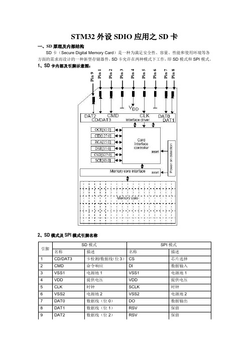
STM32外设SDIO 应用之SD 卡一、SD 原理及内部结构SD 卡(Secure Digital Memory Card )是一种为满足安全性、容量、性能和使用环境等各方面的需求而设计的一种新型存储器件,SD 卡允许在两种模式下工作,即SD 模式和SPI 模式。
1、SD 卡内部及引脚示意图:2、SD 模式及SPI 模式引脚名称P i n 3P i n 8P i n 7P i n 6P i n 5P i n 4P i n 2P i n 1P i n 93、Micro SD 引脚示意图及模式区别:二、SD 模式1、STM32的SDIO 适配器原理框图:注:R1b与R1格式相同,但可以选择在数据线上发送一个繁忙信号。
收到这些命令后,依据收到命令之前的状态,卡可能变为繁忙。
主机在收到此响应时应当检测忙状态。
R7中可接受的电压范围定义如下:6、部分命令详解CMD8用于初始化符合物理规范2.00版本的SD存储卡。
当卡处于空闲状态时,CMD8才是有效的。
该命令有两种功能:a.电压检测:检测卡是否能在主机提供的电压下工作b.扩充现有的命令及响应CMD8能通过重新定义某些现有命令的保留位,增加其新的功能。
ACMD41就是被这样被扩展后用于初始化高容量SD存储卡。
其中电源电压定义如下:当卡处于空闲状态,主机应当在发送ACMD41前发送CMD8。
在参数段,电源电压段是主机提供的电压值,而检测模式段可以是任何数值。
若主机支持卡的工作电压,卡会把接收到的电源电压及检测模式数值在命令响应中原样返回给主机。
若主机不支持卡的工作电压,卡不作响应并停留在空闲状态。
分是高容量卡(SDHC)还是标准容量卡(SDSC)。
7、SD卡寄存器SD卡寄存器有:卡识别寄存器(CID),相对卡地址寄存器(RCA),驱动级寄存器(DSR),特殊数据寄存器(CSD),SD卡配置寄存器(SCR),工作状态寄存器(OCR),SD状态寄存器(SSR),卡状态寄存器(CSR)。
SD卡原理及内部结构

1、简介:SD卡(Secure Digital Memory Card)是一种为满足安全性、容量、性能和使用环境等各方面的需求而设计的一种新型存储器件,SD卡允许在两种模式下工作,即SD模式和SPI模式,本系统采用SPI模式。
本小节仅简要介绍在SPI模式下,STM32处理器如何读写SD卡,如果读者如希望详细了解SD卡,可以参考相关资料。
SD 卡内部结构及引脚如下图所示:SD卡内部图.JPG 2、SD卡管脚图:SD卡图.JPG3、SPI模式下SD各管脚名称为:sd 卡:SPI模式下SD各管脚名称为.JPG注:一般SD有两种模式:SD模式和SPI模式,管脚定义如下:(A)、SD MODE 1、CD/DATA3 2、CMD 3、VSS1 4、VDD 5、CLK 6、VSS2 7、DATA0 8、DATA1 9、DATA2(B)、SPI MODE 1、CS 2、DI 3、VSS 4、VDD 5、SCLK 6、VSS2 7、DO 8、RSV 9、RSVSD 卡主要引脚和功能为:CLK:时钟信号,每个时钟周期传输一个命令或数据位,频率可在0~25MHz之间变化,SD卡的总线管理器可以不受任何限制的自由产生0~25MHz 的频率;CMD:双向命令和回复线,命令是一次主机到从卡操作的开始,命令可以是从主机到单卡寻址,也可以是到所有卡;回复是对之前命令的回答,回复可以来自单卡或所有卡;DAT0~3:数据线,数据可以从卡传向主机也可以从主机传向卡。
SD卡以命令形式来控制SD卡的读写等操作。
可根据命令对多块或单块进行读写操作。
在SPI模式下其命令由6个字节构成,其中高位在前。
SD卡命令的格式如表1所示,其中相关参数可以查阅SD卡规范。
4、MicroSD卡管脚图:MicroSD卡管脚图.JPG5、MicroSD卡管脚名称:MicroSD卡管脚名称.JPGSD 卡与MicroSD卡仅仅是封装上的不同,MicroSD卡更小,大小上和一个SIM卡差不多,但是协议与SD卡相同。
存储卡标准.CF.SD.SDHC.MMC.TF卡引脚定义对应关系

3
VSS1
电源地1 电源地1
4 VSS1
3 VSS1
4
VDD
电源
电源
5
6
VDD1 VDD2 4
VDD
4 VDD VDD
电源
电源
5
CLK
时钟 时钟SCK
7 CLK 5 CLK 5 CLK SCLK
时钟 时钟sck
6
VSS2
电源地2 电源地2
8 VSS2
6 VSS2
6 VSS VSS
电源地 电源地
7
DAT0
数据线0 主入从出
9 DAT0
7 DAT 7 DAT0 DO
数据线0 主入从出
8 DAT1
10 DAT1
8 DAT1
X
数据线1 保留
TF卡, 又叫 microS D卡,8 pin,外 形以及 在SD和 SPI工作 模式下 引脚定
数据线2 数据线3 命令线 电ห้องสมุดไป่ตู้ 时钟 电源地 数据线0
保留 片选/从选SS 主出从入 电源 时钟sck 电源地 主入从出
数据线1
保留
三星 MMC Micro卡 (512MB) 基本特征 卡式类型 MMC Micro 闪存卡容 量 512MB 外形尺寸 14*12*1. 1 产品重量 1 电压(V) 2.7V3.6V 其他性能 读:10 MB/s; 写:7 MB/s
SD
概念 SD卡, 数字安 全记忆 卡 (Secur
e Digital
Memory Card) ,是用 于移动 设备的 标准记 忆卡。 SD卡数 据传送 和物理 规范由 MMC发 展而 来,大 小和 MMC差 不多。 长宽和 MMC一 样,比 MMC稍 微外厚形了及 接口定 义SD卡为
SD卡引脚 电路图及工作原理介绍

SD卡引脚电路图及工作原理介绍SD卡在现在的日常生活与工作中使用非常广泛,时下已经成为最为通用的数据存储卡。
在诸如MP3、数码相机等设备上也都采用SD卡作为其存储设备。
SD卡之所以得到如此广泛的使用,是因为它价格低廉、存储容量大、使用方便、通用性与安全性强等优点。
既然它有着这么多优点,那么如果将它加入到单片机应用开发系统中来,将使系统变得更加出色。
这就要求对SD卡的硬件与读写时序进行研究。
对于SD卡的硬件结构,在官方的文档上有很详细的介绍,如SD卡内的存储器结构、存储单元组织方式等内容。
要实现对它的读写,最核心的是它的时序,笔者在经过了实际的测试后,使用51单片机成功实现了对SD卡的扇区读写,并对其读写速度进行了评估。
下面先来讲解SD卡的读写时序。
(1)SD卡的引脚定义:SD卡引脚功能详述:引脚编号SD模式SPI模式名称类型描述名称类型描述1 CD/DAT3 IO或PP 卡检测/数据线3#CS I 片选2 CMD PP 命令/回应DI I 数据输入3 V SS1S 电源地VSS S 电源地4 V DD S 电源VDD S 电源5 CLK I 时钟SCLK I 时钟6 V SS2S 电源地VSS2 S 电源地7 DAT0 IO或PP 数据线0 DO O或PP 数据输出8 DAT1 IO或PP 数据线1 RSV9 DAT2 IO或PP 数据线2 RSV注:S:电源供给I:输入O:采用推拉驱动的输出PP:采用推拉驱动的输入输出SD卡SPI模式下与单片机的连接图:SD卡支持两种总线方式:SD方式与SPI方式。
其中SD方式采用6线制,使用CLK、CMD、DAT0~DAT3进行数据通信。
而SPI方式采用4线制,使用CS、CLK、DataIn、DataOut进行数据通信。
SD方式时的数据传输速度与SPI方式要快,采用单片机对SD卡进行读写时一般都采用SPI模式。
采用不同的初始化方式可以使SD卡工作于SD方式或SPI方式。
SD卡TF卡的PCB布局布线设计要求
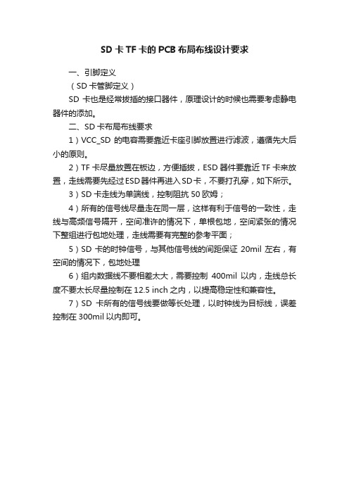
SD卡TF卡的PCB布局布线设计要求
一、引脚定义
(SD卡管脚定义)
SD卡也是经常拔插的接口器件,原理设计的时候也需要考虑静电器件的添加。
二、SD卡布局布线要求
1)VCC_SD的电容需要靠近卡座引脚放置进行滤波,遵循先大后小的原则。
2)TF卡尽量放置在板边,方便插拔,ESD器件要靠近TF卡来放置,走线需要先经过ESD器件再进入SD卡,不要打孔穿,如下所示。
3)SD卡走线为单端线,控制阻抗50欧姆;
4)所有的信号线尽量走在同一层,这样有利于信号的一致性,走线与高频信号隔开,空间准许的情况下,单根包地,空间紧张的情况下整组进行包地处理,走线需要有完整的参考平面;
5)SD卡的时钟信号,与其他信号线的间距保证20mil左右,有空间的情况下,包地处理
6)组内数据线不要相差太大,需要控制400mil以内,走线总长度不要太长尽量控制在12.5 inch之内,以提高稳定性和兼容性。
7)SD卡所有的信号线要做等长处理,以时钟线为目标线,误差控制在300mil以内即可。
SD卡原理及内部结构
1、简介:SD卡(Secure Digital Memory Card)是一种为满足安全性、容量、性能和使用环境等各方面的需求而设计的一种新型存储器件,SD卡允许在两种模式下工作,即SD模式和SPI模式,本系统采用SPI模式。
本小节仅简要介绍在SPI模式下,STM32处理器如何读写SD卡,如果读者如希望详细了解SD卡,可以参考相关资料。
SD 卡内部结构及引脚如下图所示:SD卡内部图.JPG2、SD卡管脚图:SD卡图.JPG3、SPI模式下SD各管脚名称为:sd 卡:SPI模式下SD各管脚名称为.JPG注:一般SD有两种模式:SD模式和SPI模式,管脚定义如下:(A)、SD MODE 1、CD/DATA3 2、CMD 3、VSS1 4、VDD 5、CLK 6、VSS2 7、DATA0 8、DATA1 9、DATA2(B)、SPI MODE 1、CS 2、DI 3、VSS 4、VDD 5、SCLK 6、VSS2 7、DO 8、RSV 9、RSVSD 卡主要引脚和功能为:CLK:时钟信号,每个时钟周期传输一个命令或数据位,频率可在0~25MHz之间变化,SD卡的总线管理器可以不受任何限制的自由产生0~25MHz 的频率;CMD:双向命令和回复线,命令是一次主机到从卡操作的开始,命令可以是从主机到单卡寻址,也可以是到所有卡;回复是对之前命令的回答,回复可以来自单卡或所有卡;DAT0~3:数据线,数据可以从卡传向主机也可以从主机传向卡。
SD卡以命令形式来控制SD卡的读写等操作。
可根据命令对多块或单块进行读写操作。
在SPI 模式下其命令由6个字节构成,其中高位在前。
SD卡命令的格式如表1所示,其中相关参数可以查阅SD卡规范。
4、MicroSD卡管脚图:MicroSD卡管脚图.JPG5、MicroSD卡管脚名称:MicroSD卡管脚名称.JPGSD 卡与MicroSD卡仅仅是封装上的不同,MicroSD卡更小,大小上和一个SIM卡差不多,但是协议与SD卡相同。
MMC、SD、TF、SDIO、SDMMC简介
MMC、SD、TF、SDIO、SDMMC简介MMC1. 概念MMC的全称是”MultiMediaCard”――所以也通常被叫做”多媒体卡”,是一种小巧大容量的快闪存储卡,特别应用于移动电话和数字影像及其他移动终端中。
2. 外形及接口定义如上图所示,MMC存贮卡只有7pin,可以支持MMC和SPI两种工作模式,或者换句话说:MMC是一种通信协议,支持两种模式SPI和MMC。
MMC模式是标准的默认模式,具有MMC的全部特性。
而SPI模式则是MMC存贮卡可选的第二种模式,这个模式是MMC 协议的一个子集。
如下图为MMC在各个工作模式下的引脚定义。
SD1. 概念SD卡,数字安全记忆卡(Secure Digital Memory Card),是用于移动设备的标准记忆卡。
SD卡数据传送和物理规范由MMC发展而来,大小和MMC差不多。
长宽和MMC一样,比MMC稍微厚了一点。
兼容性方面SD卡向下兼容多媒体卡(Multi Media Card)。
2. 外形及接口定义SD卡为9pinSD卡也有SD(SD有4-line和1-line两种模式,以下只列出了4-line工作模式)和SPI两种工作模式,在各个工作模式下引脚定义如下:TFTF卡,又叫microSD卡,8 pin,外形以及在SD和SPI工作模式下引脚定义如下。
SDIOSDIO是在SD内存卡接口的基础上发展起来的外设接口,SDIO 接口兼容以前的SD内存卡,并且可以连接SDIO接口的设备,目前根据SDIO协议的SPEC,SDIO接口支持的设备总类有蓝牙,网卡,电视卡等。
SDMMC经过我在百度上面的苦苦搜寻,关于SDMMC的总结如下:没有SDMMC卡或者是SDMMC接口,资料上出现SDMMC可能要表达的意思是SD/MMC,或者SDMMC是数字安全记忆卡(Secure Digital Memory Card)的简称,即SDMMC就是SD卡。
附件–(SD卡槽结构图):。
MicroSD卡(TF卡)spi模式实现方法
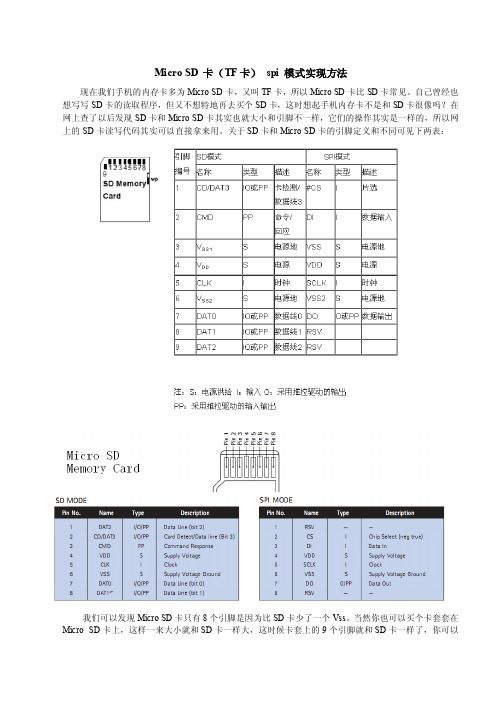
Micro SD 卡(TF卡)spi 模式实现方法现在我们手机的内存卡多为Micro SD卡,又叫TF卡,所以Micro SD卡比SD卡常见。
自己曾经也想写写SD卡的读取程序,但又不想特地再去买个SD卡,这时想起手机内存卡不是和SD卡很像吗?在网上查了以后发现SD卡和Micro SD卡其实也就大小和引脚不一样,它们的操作其实是一样的,所以网上的SD卡读写代码其实可以直接拿来用。
关于SD卡和Micro SD卡的引脚定义和不同可见下两表:我们可以发现Micro SD卡只有8个引脚是因为比SD卡少了一个Vss。
当然你也可以买个卡套套在Micro SD卡上,这样一来大小就和SD卡一样大,这时候卡套上的9个引脚就和SD卡一样了,你可以完全当做SD卡来操作。
spi下电路的连接非常简单,接上电源线Vdd和地线Vss,再接上spi的CS,SCLK,DI(MOSI)和DO(MISO)就可以了,其他引脚可以放空。
注意SD卡的电源和操作电压都为2.7-3.6V,5V的单片机要进行电平转换或串电阻限流。
还有记得SD卡的CS,SCLKh和DI要用10~100K的电阻上拉。
我是套了卡套接的电路,因为Micro SD卡的引脚太密了,不好焊接,SD卡相对引脚好焊。
因为没有卡座,而且也没专门的PCB我就直接焊到卡套上,诶牺牲了一个卡套。
下面是我自己画的电路图:上面Micro SD卡的硬件电路就好了,下面我们讲讲Micro SD卡的软件驱动和指令集。
SD卡的命令格式如下,6字节共48位,传输时最高位(MSB)先传输:SD卡的command(命令)占6 bit,一般叫CMDx或ACMDx,比如CMD1就是1,CMD13就是13,ACMD41就是41,依此类推。
Command Argument(命令参数)占4 byte,并不是所有命令都有参数,没有参数的话该位一般就用置0。
最后一个字节由7 bit CRC校验位和1 bit停止位组成。
SD卡工作原理介绍和工作原理图

SD卡工作原理介绍和工作原理图大容量SD卡在海洋数据存储中的应用本设计使用8 GB的SDHC(High Capacity SD Memory Card,大容量SD存储卡),为了方便卡上数据在操作系统上的读取,以及数据的进一步分析和处理,在SDHC卡上建立了FAT32文件系统。
海洋要素测量系统要求数据存储量大、安全性高,采用可插拔式存储卡是一种不错的选择。
目前,可插拔式存储卡有CF卡、U 盘及SD卡。
CF卡不能与计算机直接通信;U盘需要外扩接口芯片才能与单片机通信,增加了外形尺寸及功耗;而SD卡具有耐用、可靠、安全、容量大、体积小、便于携带和兼容性好等优点,非常适合于测量系统长期的数据存储。
1 SD卡接口的硬件设计STM32F103xx增强型系列是意法半导体公司生产的基于Cortex-M3的高性能的32位RISC内核,工作频率为72 MHz,O端口和连接到2条APB总线的外设。
内置高速存储器(128 KB的闪存和20 KB 的SRAM),以及丰富的增强I,STM32F103xx系列工作于-40,+105?的温度范围,供电电压为2.0,3.6 V,与SD 卡工作电压兼容,一系列的省电模式可满足低功耗应用的要求。
SD卡支持SD模式和SPI模式两种通信方式。
采用SPI模式时,占用较少的I,O资源。
STM32F103VB包含串行外设SPI接口,可方便地与SD卡进行连接。
通过4条信号线即可完成数据的传输,分别是时钟SCLK、主机输入从机输出MISO、主机输出从机输入MOSI和片选CS。
STM32F103VB与SD卡卡座的接口电路如图1所示。
SD卡的最高数据读写速度为10 MB,s,接口电压为2.7,3.6 V,具有9个引脚。
SD卡使用卡座代替传输电缆,减少了环境干扰,降低了出错率,而且1对1传输没有共享信道的问题。
SD卡在SPI模式下各引脚的定义如表1所列。
2 SD卡接口的软件设计本设计采用STM32F103VB自带的串行外设SPI接口与SD卡进行通信,这里只介绍SPI模式的通信方式。
tf卡底层引脚定义

tf卡底层引脚定义TF卡底层引脚定义:TF卡,又称为Micro SD卡,是一种常见的存储设备,广泛应用于移动设备、数码相机等领域。
TF卡底层引脚定义了TF卡与外部设备之间的连接方式和通信规则。
本文将从TF卡底层引脚定义的角度,探讨TF卡的工作原理和应用场景。
一、TF卡底层引脚定义TF卡底层引脚一般包括以下几个引脚:1. VCC:供电引脚,用于提供电源给TF卡,一般连接到3.3V或5V 电源。
2. GND:地引脚,用于连接地线,与外部设备共享地。
3. CLK:时钟引脚,用于传输时钟信号,控制数据的读写。
4. CMD:命令引脚,用于发送读写命令给TF卡。
5. DAT0-DAT3:数据引脚,用于传输数据。
二、TF卡工作原理TF卡是一种闪存存储设备,采用了SPI(Serial Peripheral Interface)或SD(Secure Digital)接口协议。
TF卡通过底层引脚与外部设备进行通信,实现数据的读写和存储。
在TF卡的工作过程中,外部设备首先通过时钟引脚(CLK)发送时钟信号给TF卡,TF卡根据时钟信号进行同步。
然后,外部设备通过命令引脚(CMD)发送读写命令给TF卡,TF卡根据命令进行相应的操作。
同时,外部设备通过数据引脚(DAT0-DAT3)与TF卡进行数据的传输。
TF卡根据命令和数据进行存储或读取操作,并将结果返回给外部设备。
三、TF卡的应用场景TF卡由于其小巧、便携的特点,在各种移动设备和数码产品中得到了广泛应用。
以下是TF卡的几个主要应用场景:1. 手机存储扩展:由于手机内置存储容量有限,用户可以通过插入TF卡来扩展手机的存储空间,方便存储大量的照片、音乐和视频等文件。
2. 数码相机存储:数码相机通常使用TF卡作为存储介质,用户可以将拍摄的照片和视频保存在TF卡中,并通过TF卡读卡器将数据传输到电脑进行编辑和存储。
3. 智能穿戴设备:智能手表、智能眼镜等智能穿戴设备中,也常常使用TF卡作为存储介质,用于存储用户的健康数据、运动轨迹等信息。
SD卡与TF卡的引脚定义

December 2007 Rev 31/61512 MByte and 1 GByte, 3.3V Supply Secure Digital™ CardFeatures■SD Memory Card Specification Version 1.01-compliant■Up to 1 Gbyte of Formatted Data Storage ■Bus Mode–SD Protocol (1 to 4 Data Lines)–SPI Protocol■Operating Voltage Range:–Basic Communication (CMD0, CMD15, CMD55 and ACMD41): 2.0V to 3.6V–Other C ommands a nd M emory A ccess: 2.7V to 3.6V ■Variable Clock Rate: 0 to 25 MHz ■Read Access (using 4 Data Lines)–Sustained Multiple Block: 6.3 Mb/s ■Write Access (using 4 Data Lines)–Sustained Multiple Block: 3.0 Mb/s ■Maximum Data Rate with up to 10 Cards ■Aimed at Portable and Stationary Applications ■Communication Channel Protocol Attributes:–Six-wire communication channel (clock, command, 4 data lines)–Error-proof data transfer–Single or Multiple block oriented data transfer■Memory Field Error Correction ■Safe Card Removal during Read■Write Protect Feature using Mechanical Switch ■Built-in Write Protection Features (Permanent and Temporary)■SD, MiniSD and MicroSD Packages –ECOPACK ® compliant –Halogen free –Antimony freeMicroSDTable 1.Device summaryPart Number Package Form Factor Operating Voltage RangeSMS128AF SD (full size)2.7V to3.6VSMS256AF SMS512AF SMS01GAF SMS064BF MiniSD SMS128BF SMS064FF MicroSDSMS128FF SMS256FF SMS512FFDescription SMSxxxAF, SMSxxxFF, SMSxxxBF1 DescriptionThe Secure Digital Memory Card (SD Memory Card) is a Flash-Based Memory Card. It is specifically designed to meet the security, capacity, performance and environmentalrequirements of the latest-generation audio and video consumer electronic devices, that is mobile phones, digital cameras, digital recorders, PDAs, organizers, electronic toys, etc. The Secure Digital Memory Card is a high-mobility, high-performance, low-cost and low-power consumption device that features high data throughput at the memory card interface. It includes a copyright protection mechanism that complies with the security of the SDMI (Secure Digital Music Initiative) standard. The Secure Digital Memory Card security system uses mutual authentication and a “cipher algorithm” that protects the card from illegal use. Unsecured access to the user's personal content is also available.The Secure Digital Memory Cards have an advanced communication interface designed to operate in a low voltage range. The full-size Secure Digital Memory Card has a 9-pin interface whereas the Mini Secure Digital Memory Card has a 11-pin interface but can be fitted with a 9-pin adapter. Only the 9-pin interface is described in this document. The MicroSD Memory Card has an 8-pin interface, and can also be fitted with a 9-pin adapter.Table 2,T able 3,Table 4,Table 5, and Table 6 give an overview of the Secure Digital Memory Card features.In order to meet environmental requirements, the devices are offered in ECOPACK ®packages. ECOPACK packages are Lead-free. The category of second Level Interconnect is marked on the package and on the inner box label, in compliance with JEDEC Standard JESD97. The maximum ratings related to soldering conditions are also marked on the inner box label.The SD, MiniSD and MicroSD packages are also Halogen free and Antimony free.Related documentation●Secure Digital Memory Card Specifications: Part 1 Physical Layer Specification, Version 1.01●MiniSd Memory Card Specifications: Addendum to SD Memory Card Specifications Part 1 Physical layer Specification, Version 1.02●MicroSD Memory Card Specifications: Addendum to SD Memory Card Specifications Part 1, Physical Layer Specification, Version 1.00Table 2.System performanceSystem performanceMax.Typ.Unit Sleep to Ready30µs Sustained Multiple Block Read (1)1.43X, 20X, 12X and 5X Speed grade markings where 1X = 150 KBytes/s.6.3 (43X)MBytes/s Burst Single Block Read (1) 1.8 (12X)MBytes/s Sustained Multiple Block Write (1) 3.0 (20X)MBytes/s Burst Single Block Write (1)0.8 (5X)MBytes/s Power-up to Ready150msSMSxxxAF, SMSxxxFF, SMSxxxBFDescriptionTable 3.Power consumption (1)1.T A = 25°C, V DD = 3.6V.ModeMax. Current ConsumptionStandby 200 µA Read 30 mA Write30 mATable 4.Environmental specifications (1)1.NA = Not Applicable; RH = Relative Humidity; ESD = ElectroStatic DischargeEnvironmental specifications Operating Non-Operating T emperature− 25°C to 85°C − 40°C to 85°C Humidity (non- condensing)NA 85°C - 85%RHESDProtectionContact PadsNA±4kV , Human body model according to ANSI EOS/ESD-S5.1-1998Other±8kV (coupling plane discharge)±15kV (air discharge) Human body model perIEC61000-4-2Salt Water Spray NA T A = 35 °C 3% NaCl (MIL Std Method 1009)Vibration (peak-to-peak)NA 15 Gmax ShockNA1,000G Drop NA2000GBending20N (middle of the card)20N (border of the card)UV light exposure254nm, 15Ws/cm2Table 5.Physical dimensionsParameter SD MiniSD MicroSD Unit Width 2420 11mmHeight3221.515 mm Thickness 2.1 1.4Inter Connect Area 0.7±0.1mmMax. Card Thickness 0.95 Max. Pull Area1.0±0.1Weight Approx. 2Approx. 1<1g Number of Pins9118N/ADescriptionSMSxxxAF, SMSxxxFF, SMSxxxBFTable 6.System reliability and maintenanceMTBF (1)1.MTBF = Mean Time Between Failures.>1,000,000hrsPreventive Maintenance NoneData Reliability 1 non-recoverable bit in 1014 bit read Endurance>2,000,000 Program/Erase CyclesSMSxxxAF, SMSxxxFF, SMSxxxBF Memory array partitioning2 Memory array partitioningThe basic unit of data transfer to/from the SD Memory Card is the Byte. The memory array is divided into several structures as described below and summarized in Table 17.BlockThe Block is the unit structure related to block-oriented read and write commands. Its size is the number of Bytes that are transferred when a block-oriented read or write command is sent by the host. The SD Memory Card Block size is either programmable or fixed. The information about allowed block sizes and programmability is stored in the CSD Register. The details of the Memory Array Structure and the number of addressable Blocks are shown in T able 17.SectorThe sector is the unit structure related to the erase commands. Its size is the number of blocks that are erased at any one time. The sector size is fixed for each device. The information about the sector size (in blocks) is stored in the CSD register.Write Protect Group (WP-Group)The WP-Group is the smallest structure that may be individually protected. Its size is the number of Sectors that are Write Protected with one bit. The information about the Write Protect Group size is stored in the CSD Register.Table 7.Memory array structuresType of Structure Number of structures in deviceUnit 32 MByte Devices 64 MByte Devices 128 MByte Devices 256 MByte Devices 512 MByte Devices 1 GByte Devices Blocks 512 Bytes 5977612262424832049971210024961999872Sector Block 128128128128128128WP-GroupsSector12481632Memory array partitioning SMSxxxAF, SMSxxxFF, SMSxxxBFSMSxxxAF, SMSxxxFF, SMSxxxBF Secure digital memory card interface3 Secure digital memory card interfaceThis section applies to the full-size SD Memory Card only, or to the MiniSD and MicroSD card when used with an adapter.Details on the 11-pin communication interface of the MiniSD card used without an adapter are still to be announced. Figure 3: MicroSD pin assignment shows the MicroSD pinout.The Secure Digital Memory Card has an advanced 9-pin communication interface (Clock, Command, 4 Data pins and 3 Power Supply pins) designed to operate in a low voltage range. The Secure Digital Card has its nine pins exposed on one side (see Figure 2). The signal/pin assignments are listed in Table 8 The pin types are Power Supply, Input, Output and Push-Pull. The signals include six communication lines CMD, DAT0, DAT1, DAT2, DAT3, CLK and three supply lines V DD , V SS1 and V SS2.Table 8.Full-size SD Memory Card pin assignmentPin #SD modeSPI modeNameType (1)1.S: power supply; I: input; O: output using push-pull drivers; PP: I/O using push-pull drivers.DescriptionName Type Description1CD/DA T3(2)2.The extended DAT lines (DAT1-DAT3) are input on power-up. They start to operate as DAT lines after SET_BUS_WIDTHcommand.I/O/PP (3)3.After power-up this line is input with 50kW pull-up (can be used for card detection or SPI mode selection). The pull-upshould be disconnected by the user, during regular data transfer, with SET_CLR_CARD_DETECT (ACMD42) command.Card Detect / Data Line [Bit 3]CS I Chip Select (active Low)2CMD PP Command/Response DI I Data In3V SS1S Supply voltage ground V SS S Supply voltage ground 4V DD S Supply voltage V DD S Supply voltage 5CLK I ClockSCLK I Clock6V SS2S Supply voltage ground V SS2SSupply voltage ground7DA T0I/O/PP Data Line [Bit 0]DOO/PP Data Out8DA T1(2)I/O/PP Data Line [Bit 1]Reserved 9DA T2(2)I/O/PPData Line [Bit 2]ReservedSecure digital memory card interfaceSMSxxxAF, SMSxxxFF, SMSxxxBFTable 9.MicroSD Contact Pad AssignmentPin SD ModeSPI ModeName Type (1)1.S: power supply; I: input; O: output using push-pull drivers; PP: I/O using push-pull drivers.Description Name TypeDescription1 DA T2 I/O/PP Data Line [Bit 2] RSV Reserved2CD/DA T3(2)2.The extended DAT lines (DAT1-DAT3) are input on power up. They start to operate as DAT lines after SET_BUS_WIDTH command. The Host shall keep its own DAT1-DAT3 lines in input mode, as well, while they are not used. It is defined so, in order to keep compatibility to MultiMediaCards.I/O/PP (3)3.After power up this line is input with 50KOhm pull-up (can be used for card detection or SPI modeselection). The pull-up should be disconnected by the user, during regular data transfer, with SET_CLR_CARD_DETECT (ACMD42) command.Card Detect / Data Line[Bit 3]CSIChip Select (neg true)3 CMD PP Command/Response DI I Data In4 V DDS Supply voltageV DD S Supply voltage 5 CLK I Clock SCLK I Clock 6 V SSSSupply voltage groundV SS SSupply voltage ground7 DA T0 I/O/PP Data Line [B it 0] DOO/PP Data Out8 DA T1RSVReservedSMSxxxAF, SMSxxxFF, SMSxxxBF Secure digital memory card interface3.1 Secure digital memory card bus topologyThe Secure Digital Memory Card system defines two alternative communications protocols:SD and SPI that correspond to two operating modes.Either mode can be selected in the application, mode selection is transparent to the host.The host automatically detects the operating mode of the card by issuing the Resetcommand (refer to Section7.2.1: Mode Selection) and will expect all furthercommunications to use the same mode. Therefore, applications that use only onecommunication mode do not have to be aware of the other.The SD bus includes the following signals:●CLK: Host to card clock signal●CMD: Bi-directional Command/Response signal●DAT0 - DAT3: 4 Bi-directional data signals.●V DD, V SS1, V SS2: Power and ground signals.The SD Memory Card bus has a synchronous star topology (refer to Figure4: Secure DigitalMemory Card system bus topology) with a single master (the application) and multipleslaves (the cards). The Clock, power and ground signals are common to all cards. Thecommand (CMD) and data (DAT0 - DAT3) signals are dedicated to the cards, they providecontinuous point-to-point connection to all the cards.During the initialization process, commands are sent to each card individually, allowing theapplication to detect the cards and assign logical addresses to the physical slots. Data isalways sent (received) to (from) each card individually. However, in order to simplify thehandling of the card stack, after the initialization process, all commands may be sentconcurrently to all cards. Addressing information is provided in the command packet.The SD bus allows dynamic configuration of the number of data lines. After power-up the SDMemory Card defaults to using only DAT0 for data transfer. After initialization the host canchange the bus width (number of active data lines). This feature is an easy trade off betweenhardware cost and system performance.Secure digital memory card interfaceSMSxxxAF, SMSxxxFF, SMSxxxBF1.DAT1 and DAT2 not connected.3.2 SD bus protocolCommunication over the SD bus is based on command and data bit streams which areinitiated by a start bit and terminated by a stop bit.●Command: a command is a token which starts an operation. A command is sent from the host either to a single card (addressed command) or to all connected cards (broadcast command). Commands are transferred serially on the CMD line. See Figure 5: "No Response" and "No Data" operations .The Command token format is shown in Figure 8●Response: a response is a token which is sent from an addressed card, or(simultaneously) from all connected cards, to the host, as an answer to a previously received command. Responses are transferred serially on the CMD line. A response is illustrated in Figure 5: "No Response" and "No Data" operations .The Response token format is shown in Figure 9●Data: data can be transferred from the card to the host or from the host to the card. Data is transferred via the data lines. See Figure 6: (Multiple) Block Read operation for an illustration.The Data Packet format is shown in Figure 10Card addressing is implemented using a session address assigned to the card during the initialization phase (See SD Memory Card Specification, Chapter 4). The basic transaction on the SD bus is the command/response transaction. In this type of bus transactions, the information is directly transferred within the command or response structure. In addition, some operations have a data token. Data transfers to/from the SD Memory Card are done in blocks. Data blocks are always followed by CRC bits.Single and Multiple Block operations are supported. Note that the Multiple Block operation mode improves the speed of write operations. A Multiple Block transmission is terminated by issuing a STOP_TRANSMISSION command on the CMD line (See Figure 6 and Figure 7).Data transfer can be configured by the host to use single or multiple data lines (provided that the card supports this feature).A busy signal on DAT0 is used to indicate that a Block Write operation is ongoing (see Figure7). The same busy signaling is used regardless of the number of data lines used to transfer the data.Response tokens (see Figure9) have four coding schemes depending on their content. The token length is either 48 or 136 bits (See SD Memory Card Specification, Chapter 4.5 for detailed definitions of the commands and responses). The CRC protection algorithm for data block is a 16-bit CCITT polynomial (see SD Memory Card Specification, chapter 4.5). On the CMD line, the MSB bit is transmitted first and the LSB bit last. When the wide bus option is used, the data is transferred 4 bits at a time (refer to Figure10). Start bits, End bits and CRC bits, are transmitted on all the DAT lines used. CRC bits are calculated and checked for every DAT line individually. The CRC status response and Busy indication are sent by the card to the host on DAT0 only (DAT1-DAT3 are Don’t Care).3.3 SD Memory Card Functional DescriptionAll communications between the host and the cards are controlled by the host (master).The host sends commands of two types:●Broadcast commands which are intended for all cards. Some of these commandsrequire a response.●Addressed (point-to-point) commands that are sent to the addressed card and arefollowed by a response from the card.Modes3.4 OperationFigure11 and Figure12 show an overview of the command flow for the Card Identificationmode and the Data Transfer mode, respectively.Table10 shows the relationship between operation modes and card states. Each state in theSD Memory Card state diagram (see Figure16 and Figure17) is associated with oneoperation mode.Table 10.Card States vs. Operation ModesCard state Operation modeInactive State InactiveIdle StateReady StateCard Identification ModeIdentification State3.4.1 Card Identification ModeThe host enters the Card Identification mode after reset and remains in this mode until it hasfinished searching for new cards on the bus.Cards enter the Card Identification mode after reset and remain in this mode until they receive the SEND_RCA command (CMD3) (or the SET_RCA command for MultiMediaCards).While in Card Identification mode the host resets all the cards that are in Card Identification mode, validates the operation voltage range, identifies every card and asks them to publish their Relative Card Addresses (RCA). This operation is done separately for each card on its own CMD line. In this mode, all data communications use the command line (CMD) only.The host starts the card identification process at the identification clock rate f OD . The SD Memory Card has push-pull CMD line output drives.Once the bus has been activated the host asks each card to send their valid operation conditions (ACMD41 preceded by APP_CMD - CMD55 with RCA=0000h).The response to ACMD41 is the Operation Condition Register of the card. The same command is sent to all the new cards in the system. Incompatible cards are switched to Inactive State.The host then issues the ALL_SEND_CID command (CMD2), to every card to get their unique card identification (CID) numbers. All unidentified cards (which are in Ready State) answer by sending their CID numbers (on the CMD line) and switch to the Identification State. Then the host issues a CMD3 (SEND_RELATIVE_ADDR) command to ask the cards to publish a relative card address (RCA). The RCA is shorter than the CID, and will be used to address the card (typically at a clock rate higher than f OD ) once this is in Data Transfer mode. Once the RCA is received the card state changes to Standby. At this point, the host may ask the card to publish another RCA number by sending anotherSEND_RELATIVE_ADDR command to the card. The last published RCA is the actual RCA of the card.The host repeats the identification process, that is the cycles with CMD2 and CMD3, for each card in the system. Once all the SD Memory Cards have been initialized, the host initializes the MultiMediaCards that are in the system (if any) by issuing CMD2 and CMD3 as explained in the MultiMediaCard specification. Note that in the SD system all the cards are connected separately so each MultiMediaCard has to be initialized individually.Stand-by State Data Transfer ModeT ransfer State Sending-data State Receive-data State Programming State Disconnect StateTable 10.Card States vs. Operation Modes (continued)Card stateOperation mode3.4.2 Data Transfer ModeCards enter the Data Transfer mode once their Relative Card Addresses (RCA) have beenpublished.The host enters the Data Transfer mode after identifying all the cards on the bus.The host issues SEND_CSD (CMD9) to obtain the contents of the Card Specific Data (CSD)Register for each card. The CSD Register contains information like the block length and thecard storage.Until the host knows the contents of all the CSD Registers, the f PP clock rate must remain atf OD because some cards may have operating frequency limitations.The broadcast command SET_DSR (CMD4) configures the driver stages of all identifiedcards. It programs their Driver Stage Registers (DSR) according to the application buslayout (length), the number of cards on the bus and the data transfer frequency. The clockrate is changed from f OD to f PP at that point. The SET_DSR command is an option for thecard and the host.CMD7 is used to select one card and switch it to the Transfer State. Only one card can be inTransfer State at a given time. If a previously selected card is still in Transfer State when thehost uses CMD7 to switch another card to the Transfer state, then the connection betweenthe previously selected card and the host is released and the card reverts to the StandbyState.When CMD7 is issued with the reserved relative card address "0000h", all cards revert to the Standby State. This function may be used before identifying new cards, to avoid resetting already registered cards. When in Standby state the cards that already have an RCA do not respond to identification commands (CMD41, CMD2, CMD3).Note that a card is deselected when it receives a CMD7 with an RCA that does not match. Card deselection is automatic if another card in a system is selected and the cards share the same CMD lines.So, in an SD Memory Card system, the host may either have a common CMD line for all SD Memory Cards (in which case card deselection is automatic just like in a MultiMediaCard system) or the host may have separate CMD lines, in which case it must be aware of the necessity of deselecting cards.All data communications in the Data Transfer Mode are point-to point between the host and the selected card (using addressed commands). All addressed commands are acknowledged by a response on the CMD line.The relationships between the various states in the Data Transfer mode are summarized below (see Figure12):●All Data Read commands (CMD17, CMD18, CMD30, CMD56, ACMD51) can beaborted at any time using the Stop command (CMD12). The data transfer will terminate and the card will return to the T ransfer State.●All Data Write commands (CMD24,CMD25, CMD26, CMD27, CMD42, CMD56) can beaborted at any time using the Stop command (CMD12). The write commands must be stopped prior to deselecting the card using CMD7.●As soon as the data transfer has completed, the card switches from the Data Writestate to either the Programming state (if the transfer was successful) or the T ransfer state (if the transfer failed).●If a Block Write operation is stopped and the block length and CRC of the last block arevalid, the data will be programmed.●The card can provide buffering during Block Write. This means that the data to beprogrammed to the next block can be sent to the card while the previous block is being programmed.If all write buffers are full, the DAT0 line will remain Low (BUSY) as long as the card is in the Programming state (see Figure12).●There is no buffering option for Write CSD, Write CID, Write Protection and erase. Thismeans that while the card is busy with any one of these commands, no other Data Transfer command will be accepted. The DAT0 line will remain Low as long as the card is busy and in the Programming state.●Parameter Set commands (CMD16, CMD32, CMD33) are not allowed while the card isprogramming.●Read commands are not allowed while the card is programming.●Switching another card from the Standby to the Transfer state (using CMD7) will notterminate erase and programming operations. The card will switch to the Disconnect state and release the DAT line.● A card in the Disconnect state can be reselected using CMD7. The card will then revertto the Programming state and reactivate the busy signaling.●Resetting a card (using CMD0 or CMD15) will terminate any pending or ongoingprogramming operation. This may result in the loss of card contents. It is up to the host to prevent possible data loss.3.5 CommandsFour types of commands are used to control the SD Memory Card:1.Broadcast commands (bc), no response: The broadcast feature is available only ifall the CMD lines are interconnected at the level of the host. If they are notinterconnected then each individual card will accept the command in turn.2. Broadcast commands with response (bcr): Since there is no Open Drain mode inSD Memory Cards, this type of command is used only if the host does not use acommon CMD line. The command is accepted by every individual Card and theresponses from all cards are sent simultaneously.3. addressed (point-to-point) commands (ac): There is no data transfer on DAT.4. addressed (point-to-point) data transfer commands (adtc): There is a data transferon DAT.All commands have a fixed code length of 48 bits for a transmission time of 2.4µs at 20MHz.All commands and responses are sent over the CMD line of the SD Memory Card.Command transmission always starts with the most significant bit (MSB) of the commandcodeword. All commands are protected by a CRC. All Command codewords are terminatedby the end bit (always '1'). T able11 shows the command format. All commands and theirarguments are specified in the SD Memory Card Specification.Table 11.SD Card Command Format3.6 ResponsesAll responses are sent via the command line CMD. Response transmission always starts with the leftmost bit of the response codeword. The code length depends on the response type. A response always starts with a start bit (always '0'), followed by the bit indicating the direction of transmission (from card = '0').A value denoted by 'X' in T able 12,Table 13,T able 14 and Table 15 indicates a variable entry.All responses (except for R3 Responses) are protected by a CRC. All response codewords are terminated by the end bit (always '1').There are five types of responses. Their formats are defined as follows:1.R1 (normal response command): the code length is 48 bits. Bits 45 to 40 indicate the index of the command to respond to. The index is a binary coded number (between 0 and 63). The status of the card is coded in 32 bits (see Table 12).Note that if data transfer to the card takes place, then a busy signal may appear on the data line after the transmission of each block of data. The host has to check for busy after data block transmission. 2.R1b is identical to R1 with an optional busy signal transmitted on the data line. The card may become busy after receiving these commands, depending on the state it was in prior to receiving the command. The Host has to check for busy in the response.3.R2 (CID, CSD Register): the code length is 136 bits. The contents of the CID Register are sent as a response to the CMD2 and CMD10 commands. The contents of the CSD Register are sent as a response to CMD9. Only the bits [127...1] of the CID and CSD Registers are transferred, the reserved bit [0] of these registers is replaced by the end bit of the response (see Table 13).4. R3 (OCR register): the code length is 48 bits. The contents of the OCR register are sent as a response to ACMD41 (see Section Table 14. on page 25).5.R6 (Published RCA response): the code length is 48 bits. Bits 45 to 40 indicate the index of the command to respond to. In this case it is '000011' (together with bit 5 in the status bits it means = CMD3) as shown in Table 15 The 16 MSB bits of the argument field are used for the Published RCA number.For more details about Response formats, please refer to the SD Memory Card Specification.Bit position 474645:4039:87:10Width 1163271Value '0''1'x x x '1'DescriptionStart bitT ransmissionbitCommand indexArgumentCRC7End bitTable 12.Response R1Table 13.Response R2Table 14.Response R3Table 15.Response R6Bit Position 4746[45:40][39:8][7:1]0Width (bits)1163271Value ‘0’‘0’X X X ‘1’DescriptionStart BitTransmissionBitCommand IndexCard StatusCRC7End BitBit Position 135134[133:128][127:1]0Width (bits)1161271Value ‘0’‘0’‘111111’X ‘1’DescriptionStart BitTransmission BitReservedCID or CSD register incl. internal CRC7End BitBit Position 4746[45:40][39:8][7:1]0Width (bits)1163271Value ‘0’‘0’‘111111’X ‘111111’‘1’DescriptionStart BitTransmissionBitReservedOCR RegisterReservedEnd BitBit Position 4746[45:40][39:8] Argument Field [7:1]0Width (bits)116161671Value ‘0’‘0’X X X X ‘1’DescriptionStart BitT ransmission BitCommand Index (‘000011’)New published RCA [31:16] of the card[15:0] Card Status Bits: 23, 22, 19 and 12 to 0CRC7end bit。
内存卡区别

SD卡分TF(micro-SD)卡和SD卡两种。
TF(micro-SD)卡——迷你卡(用于手机,就是卡芯【指甲盖大小】)
SD卡——正常卡(用于相机)
CF卡
记忆棒/XQD卡
WIFI卡
1. TF卡又名MicroSD卡,体积非常小,多用于手机,MP4等对于性能要求不高的数码设备,不适合单反(当然也有高性能的UHS-1卡)。
2. SD卡是目前最通用的储存卡,各种价位都有,很多电脑自带SD卡插槽,卡片机和单反都能用。
3. CF卡总体性能较SD卡要高,用于单反等对性能要求高的设备,体积较大。
4. 记忆棒是索尼专有的规格,貌似也只有索尼的相机能用了。
5. 所谓“WIFI卡”也就是带wifi功能的SD卡,相机拍完照可以通过wifi把照片在手机或电脑上上显示或者传输,也有性能较高的。