4012 CMOS 双4输入与非门
4000系列芯片功能(名称)介绍
4000系列芯片功能(名称)介绍4000 双输入或非门加反相器4001 四2输入或非门4002 双四输入或非门4006 18位移位寄存器,串行输入串行输出4007 双CMOS对加反相器4008 4位全加算术运算单元4009 16进制反相器4010 16位缓冲器4011 四2输入与非门4012 双4输入与非门4013 双D触发器4014 8级移位寄存器,并行输入串行输出4015 双4级移位寄存器,串行输入并行输出(与74HC4015同)4016 四双向模拟开关4017 十进制计数器,十选一同步输出4018 可编程计数器(环形计数)4019 四刀双掷数据选择器4020 14级二进制脉冲计数器(和74HC4020同)4021 8级移位寄存器,并行输入,串行输出4022 8进制计数器,八选一输出4023 三3输入与非门4024 7级二进制脉冲计数器,与74HC4024同4025 三3输入或非门4026 带使能端的十进制计数器和七段解码器4027 带预置和清零的双JK触发器4028 十选一解码器4029 递增——递减同步计数器,十进制或十六进制4030 异或门,使用4077或45074031 64级移位寄存器,串行输入并行输出4032 三加法器,正逻辑算术运算单元4033 十进制计数器和带消隐的七段译码器4034 八位双向存储寄存器4035 四级移位寄存器,并行输入并行输出4038 三加法器,负逻辑算术运算单元4040 12级二进制脉冲计数器(与74HC4040同)4041 四反相/非反相缓冲器4042 四D型锁存器4043四触发器,RS或非逻辑4044 四触发器,RS与非逻辑4046 锁相环,专用器件4047 双稳态与单稳态多谐振荡器4049 16进制反相器/转换器(与74HC4049同)4050 16位缓冲器/转换器4051 8选1模拟开关(与74HC4051同)4052 双4选1模拟开关(与74HC4052同)4053 三3选1模拟开关(与74HC4053同)4060带振荡器的14级二进制脉冲计数器(与74HC4060同)4063 14位振幅比较器运算单元4066 四模拟开关,低阻抗(与74HC4066同)4067 16选1模拟开关4068 8输入与非门4069 16进制反相器4070 四异或门4071 四2输入或门4072 双4输入或门4073 三3输入与门4075 三3输入或门(与74HC4075同)4076 4级三态存储寄存器4077 四2输入同或门4078 8输入与非门4081 四2输入与门4082 双4输入与门4089 二进制系数乘法器4093 四2输入与非施密特触发器4097 双8选1模拟开关4098 双单稳态触发器4099 8位可寻址锁存器40100 32位左/右移位寄存器40101 9位奇偶较验器40102 8位可预置同步BCD减法计数器40103 8位可预置同步二进制减法计数器40104 4位双向移位寄存器40105 先入先出FI-FD寄存器40106 六施密特触发器40107 双2输入端与非缓冲/驱动器40108 4字×4位多通道寄存器40109 四低-高电平位移器40110 十进制加/减,计数,锁存,译码驱动40147 10-4线编码器40160 可预置BCD加计数器40161 可预置4位二进制加计数器40162 BCD加法计数器40163 4位二进制同步计数器40174 六锁存D型触发器40175 四D型触发器40181 4位算术逻辑单元/函数发生器40182 超前位发生器40192 可预置BCD加/减计数器(双时钟) 40193 可预置4位二进制加/减计数器40194 4位并入/串入-并出/串出移位寄存40195 4位并入/串入-并出/串出移位寄存40208 4×4多端口寄存器。
CD4012中文资料

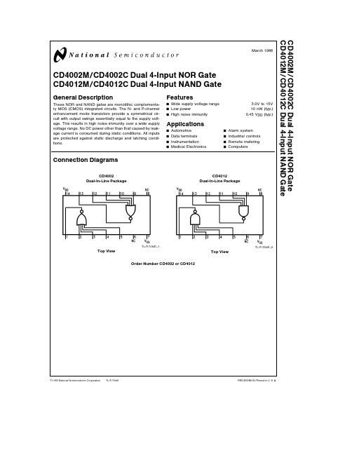
TL F 5940CD4002M CD4002C Dual 4-Input NOR Gate CD4012M CD4012C Dual 4-Input NAND GateMarch 1988CD4002M CD4002C Dual 4-Input NOR Gate CD4012M CD4012C Dual 4-Input NAND GateGeneral DescriptionThese NOR and NAND gates are monolithic complementa-ry MOS (CMOS)integrated circuits The N-and P-channel enhancement mode transistors provide a symmetrical cir-cuit with output swings essentially equal to the supply volt-age This results in high noise immunity over a wide supply voltage range No DC power other than that caused by leak-age current is consumed during static conditions All inputs are protected against static discharge and latching condi-tionsFeaturesY Wide supply voltage range 3 0V to 15V Y Low power10nW (typ )YHigh noise immunity0 45V DD (typ )ApplicationsY Automotive Y Alarm system Y Data terminals Y Industrial controls Y Instrumentation Y Remote metering YMedical ElectronicsYComputersConnection DiagramsCD4002Dual-In-Line PackageTL F 5940–1Top ViewCD4012Dual-In-Line PackageTL F 5940–2Top ViewOrder Number CD4002or CD4012C 1995National Semiconductor Corporation RRD-B30M105 Printed in U S AAbsolute Maximum Ratings(Note1)If Military Aerospace specified devices are required please contact the National Semiconductor Sales Office Distributors for availability and specifications Voltage at Any Pin V SS b0 3V to V DD a0 3V Operating Temperature RangeCD4002M CD4012M b55 C to a125 C CD4002C CD4012C b40 C to a85 C Storage Temperature Range(T S)b65 C to a150 C Power Dissipation(P D)Dual-In-Line700mW Small Outline500mW Operating Range(V DD)V SS a3 0V to V SS a15V Lead Temperature(T L)(Soldering 10seconds)260 CDC Electrical Characteristics CD4002M CD4012MLimitsSymbol Parameter Conditions b55 C a25 C a125 C UnitsMin Max Min Typ Max Min MaxI DD Quiescent V DD e5 0V0 050 0010 053 0m ADevice Current V DD e10V0 10 0010 16m A P D Quiescent Device V DD e5 0V0 250 0050 2515m W Dissipation Package V DD e10V1 00 011 060m W V OL Output Voltage V DD e5 0V V I e V DD I O e0A0 0500 050 05V Low Level V DD e10V V I e V DD I O e0A0 0500 050 05V V OH Output Voltage V DD e5 0V V I e V SS I O e0A4 954 955 04 95V High Level V DD e10V V I e V SS I O e0A9 959 95109 95V V NL Noise Immunity V DD e5 0V V O e3 6V I O e0A1 51 52 251 4V (All Inputs)V DD e10V V O e7 2V I O e0A3 03 04 52 9V V NH Noise Immunity V DD e5 0V V O e0 95V I O e0A1 41 52 251 5V (All Inputs)V DD e10V V O e2 9V I O e0A2 93 04 53 0V I D N Output Drive Current V DD e5 0V V O e0 4V V I e V DD0 50 401 00 28mAN-Channel(4002)V DD e10V V O e0 5V V I e V DD1 10 92 50 65mA (Note2)I D P Output Drive Current V DD e5 0V V O e2 5V V I e V SS b0 62b0 5b2 0b0 35mAP-Channel(4002)V DD e10V V O e9 5V V I e V SS b0 62b0 5b1 0b0 35mA (Note2)I D N Output Drive Current V DD e5 0V V O e0 4V V I e V DD0 310 250 50 175mAN-Channel(4012)V DD e10V V O e0 5V V I e V DD0 630 50 60 35mA (Note2)I D P Output Drive Current V DD e5 0V V O e2 5V V I e V SS b0 31b0 25b0 5b0 175mAP-Channel(4012)V DD e10V V O e9 5V V I e V SS b0 75b0 6b1 2b0 4mA (Note2)I I Input Current10pANote1 ‘‘Absolute Maximum Ratings’’are those values beyond which the safety of the device cannot be guaranteed Except for‘‘Operating Temperature Range’’they are not meant to imply that the devices should be operated at these limits The table of‘‘Electrical Characteristics’’provides conditions for actual device operationNote2 I D N and I D P are tested one output at a time2DC Electrical Characteristics CD4002C CD4012CLimitsSymbol Parameter Conditions b55 C a25 C a85 C UnitsMin Max Min Typ Max Min MaxI DD Quiescent V DD e5 0V0 50 0050 515m ADevice Current V DD e10V5 00 0055 030m A P D Quiescent Device V DD e5 0V2 50 0252 575m W Dissipation Package V DD e10V500 0550300m W V OL Output Voltage V DD e5 0V V I e V DD I O e0A0 0500 050 05V Low Level V DD e10V V I e V DD I O e0A0 0500 050 05V V OH Output Voltage V DD e5 0V V I e V SS I O e0A4 954 955 04 95V High Level V DD e10V V I e V SS I O e0A9 959 95109 95V V NL Noise Immunity V DD e5 0V V O t3 6V I O e0A1 51 52 251 4V (All Inputs)V DD e10V V O t7 2V I O e0A3 03 04 52 9V V NH Noise Immunity V DD e5 0V V O s0 95V I O e0A1 41 52 251 5V (All Inputs)V DD e10V V O s2 9V I O e0A2 93 04 53 0V I D N Output Drive Current V DD e5 0V V O e0 4V V I e V DD0 350 31 00 24mAN-Channel(4002)V DD e10V V O e0 5V V I e V DD0 720 62 50 48mA (Note2)I D N Output Drive Current V DD e5 0V V O e0 4V V I e V DD0 1450 120 50 095mAN-Channel(4012)V DD e10V V O e0 5V V I e V DD0 30 250 60 2mA (Note2)I D P Output Drive Current V DD e5 0V V O e2 5V V I e V SS b0 35b0 3b2 0b0 24mAP-Channel(4002)V DD e10V V O e9 5V V I e V SS b0 3b0 25b1 0b0 2mA (Note2)I D P Output Drive Current V DD e5 0V V O e2 5V V I e V SS b0 145b0 12b0 5b0 095mAP-Channel(4012)V DD e10V V O e9 5V V I e V SS b0 35b0 3b1 2b0 24mA (Note2)I I Input Current10pANote1 ‘‘Absolute Maximum Ratings’’are those values beyond which the safety of the device cannot be guaranteed Except for‘‘Operating Temperature Range’’they are not meant to imply that the devices should be operated at these limits The table of‘‘Electrical Characteristics’’provides conditions for actual device operationNote2 I D N and I D P are tested one output at a time3AC Electrical Characteristics T A e25 C C L e15pF and input rise and fall times e20ns Typical temperature coefficient for all values of V DD e0 3% CSymbol Parameter Conditions Min Typ Max Units CD4002Mt PHL Propagation Delay Time V DD e5 0V3550ns High to Low Level V DD e10V2540ns t PLH Propagation Delay Time V DD e5 0V3550ns Low to High Level V DD e10V2540ns t THL Transition Time High V DD e5 0V65175ns to Low Level V DD e10V3575ns t TLH Transition Time Low V DD e5 0V65125ns to High Level V DD e10V3570nsC IN Input Capacitance Any Input5 0pFCD4002Ct PHL Propagation Delay Time V DD e5 0V35120ns High to Low Level V DD e10V2565ns T PLH Propagation Delay Time V DD e5 0V3580ns Low to High Level V DD e10V2555ns t THL Transition Time High V DD e5 0V65300ns to Low Level V DD e10V35125ns t TLH Transition Time Low V DD e5 0V65200ns to High Level V DD e10V35115nsC IN Input Capacitance Any Input5 0pFAC Parameters are guaranteed by DC correlated testingAC Electrical Characteristics T A e25 C C L e15pF and input rise and fall times e20ns Typical temperature coefficient for all values of V DD e0 3% CSymbol Parameter Conditions Min Typ Max Units CD4012Mt PHL Propagation Delay Time V DD e5 0V5075ns High to Low Level V DD e10V2540ns t PLH Propagation Delay Time V DD e5 0V5075ns Low to High Level V DD e10V2540ns t THL Transition Time High V DD e5 0V75125ns to Low Level V DD e10V5075ns t TLH Transition Time Low V DD e5 0V75100ns to High Level V DD e10V4060nsC IN Input Capacitance Any Input5 0pFCD4012Ct PHL Propagation Delay Time V DD e5 0V50100ns High to Low Level V DD e10V2550ns T PLH Propagation Delay Time V DD e5 0V50100ns Low to High Level V DD e10V2550ns t THL Transition Time High V DD e5 0V75150ns to Low Level V DD e10V50100ns t TLH Transition Time Low V DD e5 0V75125ns to High Level V DD e10V4075nsC IN Input Capacitance Any Input5 0pFAC Parameters are guaranteed by DC correlated testingNote1 ‘‘Absolute Maximum Ratings’’are those values beyond which the safety of the device cannot be guaranteed Except for‘‘Operating Temperature Range’’they are not meant to imply that the devices should be operated at these limits The table of‘‘Electrical Characteristics’’provides conditions for actual device operation4Physical Dimensions inches(millimeters)Ceramic Dual-In-Line Package(J)Order Number CD4002MJ CD4002CJ CD4012MJ or CD4012CJNS Package Number J14A5C D 4002M C D 4002C D u a l 4-I n p u t N O R G a t e C D 4012M C D 4012C D u a l 4-I n p u t N A N D G a t ePhysical Dimensions inches (millimeters)(Continued)Molded Dual-In-Line Package (N)Order Number CD4002MN CD4002CN CD4012MN or CD4012CNNS Package Number N14ALIFE SUPPORT POLICYNATIONAL’S PRODUCTS ARE NOT AUTHORIZED FOR USE AS CRITICAL COMPONENTS IN LIFE SUPPORT DEVICES OR SYSTEMS WITHOUT THE EXPRESS WRITTEN APPROVAL OF THE PRESIDENT OF NATIONAL SEMICONDUCTOR CORPORATION As used herein 1 Life support devices or systems are devices or 2 A critical component is any component of a life systems which (a)are intended for surgical implant support device or system whose failure to perform can into the body or (b)support or sustain life and whose be reasonably expected to cause the failure of the life failure to perform when properly used in accordance support device or system or to affect its safety or with instructions for use provided in the labeling can effectivenessbe reasonably expected to result in a significant injury to the userNational Semiconductor National Semiconductor National Semiconductor National Semiconductor CorporationEuropeHong Kong LtdJapan Ltd1111West Bardin RoadFax (a 49)0-180-530858613th Floor Straight Block Tel 81-043-299-2309。
40系列管脚图
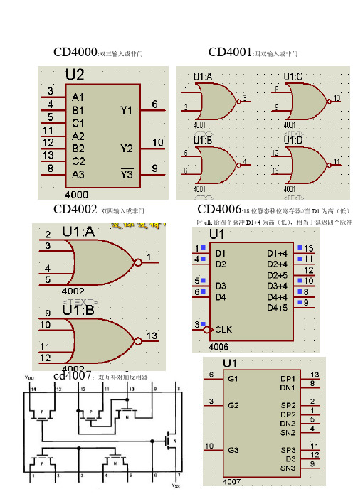
CD4000:双三输入或非门CD4001:四双输入或非门CD4002双四输入或非门CD4006:18位静态移位寄存器//当D1为高(低)时clk给四个脉冲D1+4为高(低),相当于延迟四个脉冲cd4007:双互补对加反相器CD4008:并行进位输出全加器CD4009:六缓相器/转换-倒相CD4010:六缓相器/转换-正相CD4011四2输入端与非门CD4012双4输入端与非门CD4013双主-从D型触发器CD4014 8位串入/并入-串出移位寄存器CD4015双4位串入/并出移位寄存器CD4016四传输门CD4017十进制计数/分配器CD4018可预制1/N计数器//当PE为高时并行输入数据,与clk无关,PE为低时D输入并移位CD4019四与或选择器CD4020 14级串行二进制计数/分频器clk给八个下降沿Q3开始计数CD4021 08位串入/并入-串出移位寄存器当9脚为同时D5-D7并行输入数据且与时钟无关,当其为低电平时从D4数据开始移位,SIN数据迟后六个脉冲CD402八进制计数/分配器CD4023三3输入端与非门CD4024 7级二进制串行计数/分频器CD4025三3输入端或非门CD4026十进制计数/7段译码器当2和15为低3为高时,数码管随脉冲0-1-2…9-02脚为高电平时计数锁存脚5.4.14一般为高显9时5脚为低显2时14脚为低4脚与3脚一至CD4027双J-K触发器CD4028 BCD码十进制译码器当jk同时为1时Qn+1=Qn’CD4029可预置可逆计数器CD4030四异或门当输入全部为低时,只给clk时钟,输出从9到0计数co平时为高输出为0时其为低,当只有10脚为高时给Clk电路从0到9计数,co只在显9时为低。
5脚为高电平则锁存。
1脚为高则并行置数·CD4033 十进制计数/7段译码器CD4034 8位通用总线寄存器CD4035 4位并入/串入-并出/串出移位寄存CD4038三串行加法器CD4040 12级二进制串行计数/分频器CD4041四同相/反相缓冲器脚1为脚3的同相输出,脚2为脚3的反相输出CD4042四锁存D型触发器CD4043 4三态R-S锁存触发器("1"触发) CD4044四三态R-S锁存触发器("0"触发) CD4046锁相环\\见资料CD4047无稳态/单稳态多谐振荡器\\见资料CD4048 4输入端可扩展多功能门\\见资料CD4049六反相缓冲/变换器CD4050六同相缓冲/变换器CD4051八选一模拟开关CD4052双4选1模拟开关6脚为低电平时有效;6脚为低电平时无效CD4053三组二路模拟开关只要A为1,NH CD4054 液晶显示驱动器为低x=x1;若A为0;INH为低不管BCX=x0CD4055 BCD-7段译码/液晶驱动器CD4056液晶显示驱动器当6脚为高电平时输出反码CD4059“N”分频计数器CD4060 14级二进制串行计数/分频器CD4063四位数字比较器CD4066四传输门CD4067 16选1模拟开关CD4068八输入端与非门/与门4069六反相器CD4070四异或门CD4071四2输入端或门CD4072双4输入端或门CD4073三3输入端与门CD4075三3输入端或门CD4076四D寄存器\\见资料CD4077四2输入端异或非门CD4078 8输入端或非门/或门CD4081四2输入端与门CD4082双4输入端与门CD4093四2输入端施密特触发器CD4085双2路2输入端与或非门CD4094 8位移位存储总线寄存器CD4095 3输入端J-K触发器STB为高时则将移位的数据显示出来,STB为低时输出保持不变,移位在工作只是没有显出来,要等到下次STB为高时才显出来,相当于74595的两个时钟CD4096 3输入端J-K触发器CD4098双单稳态触发器CD4099 8位可寻址锁存器CD40105先入先出FI-FD寄存器CD40106六施密特触发器CD40110十进制加/减,计数,锁存,译码驱动CD40160可预置BCD加计数器CD40161可预置4位二进制加计数器CD40162 BCD加法计数器CD40163 4位二进制同步计数器CD40174六锁存D型触发器CD40175四D型触发器CD40192可预置BCD CD40193可预置4位二进制CD40194 4位并入/串入-并加/减计数器(双时钟) 加/减计数器出/串出移位寄存CD4502可选通三态输出六反相/缓冲器CD4503六同相三态缓冲器CD4508双4位锁存D型触发器//12脚为低反相CD4510可预置BCD码加/减计数器CD4511 BCD锁存,7段译码,驱动器CD4512八路数据选择器CD4513 BCD锁存,7段CD4514 4位锁存,4线-16CD4515 4位锁存,4线-16 译码,驱动器(消隐) 线译码器线译码器CD4516可预置4位二进制加/减计数器CD4518双BCD同步加计数器CD4520双4位二进制同步加计数器CD4522可预置BCD同步1/N计数器CD4526可预置4位二进制同步1/N计数器CD4528双单稳态触发器CD4529双四路/单八路模拟开关CD4530双5输入端优势逻辑门CD4532 8位优先编码器CD4538精密双单稳CD4539双四路数据选择器CD4541 可编程序振荡/计时器CD4543BCD七段锁存译码,驱动器CD4553三位BCD计数器CD4555双二进制四选一译码器/分离器CD4556双二进制四选CD4560 "N"BCD加法器CD4584六施密特触发器一译码器/分离器CD4585 4位数值比较器。
40系列CMOS电路型号功能

40193 CMOS 可预制四位二进制计数器
40194 CMOS 4位双向并行存取通用移位寄存器
4020 CMOS 14级二进制串行计数/分频器
40208 CMOS 4×4多端寄存器
4021 CMOS 异步8位并入同步串入/串出寄存器
4022 CMOS 八进制计数器/分频器
4010 CMOS 六缓冲器/转换器(同相)
40100 CMOS 32位双向静态移位寄存器
40101 CMOS 9位奇偶发生器/校验器
40102 CMOS 8位BCD可预置同步减法计数器
40103 CMOS 8位二进制可预置同步减法计数器
40104 CMOS 4位三态输出双向通用移位寄存器
40105 CMOS 先进先出寄存器
40106 CMOS 六施密特触发器
40107 CMOS 2输入双与非缓冲/驱动器
40108 CMOS 4×4多端寄存
40109 CMOS 四三态输出低到高电平移位器
4011 CMOS 四2输入与非门
40110 CMOS 十进制加减计数/译码/锁存/驱动
4035 CMOS 4位并入/并出移位寄存器
4038 CMOS 3位串行负逻辑加法器
4040 CMOS 12级二进制计数/分频器
4041 CMOS 四原码/补码缓冲器
4042 CMOS 四时钟控制 D 锁存器
4043 CMOS 四三态或非 R/S 锁存器
4502 CMOS 可选通六反相缓冲器
4503 CMOS 六三态同相缓冲器
4504 CMOS 六TTL-CMOS电平移位器
4506 CMOS 双二组2输入可扩展与或非门
CC4012中文资料

华强电子网
引出端排列(俯视)
逻辑图(1/2)
逻辑表达式
华强电子网
静态特性:
参数 VO (V) 测试条件 VI VDD -55℃ (V) (V) 5/0 5.0 10/0 10.0 15/0 15.0 5/0 10/0 15/0 5.0 10.0 15.0 5.0 10.0 15.0 5.0 10.0 15.0 5.0 5.0 10.0 15.0 5.0 10.0 15.0 15.0 5.0 10.0 15.0 0.25 0.5 1.0 -2.0 -0.64 -1.6 -4.2 0.64 1.6 4.2 -1.8 -0.61 -1.5 -4.0 0.61 1.5 4.0 ±0.1 0.25 0.5 1.0 -40℃ 规范值 25℃ 85℃ 0.05 125℃ 单位 V
CC4012------双4输入与非门 概述: CC4011 为 4 输入正向逻辑与非门。 CC4011 与非门为系统设计者提供了直接的与非功能,补充了已有 COS/MOS 门系列,所有输入和输出经过缓冲,改善了输入/输出传输特性,使得由于负载容量 的增加而引起的传输时间的变化维持到最小。
提供了 14 引线多层陶瓷双列直插(D)、熔封陶瓷双列直插(J)、塑料双列直插 (P)和陶瓷片状载体(C)4 种封装形式。
5.0 10.0 15.0 5.0 10.0 15.0
5.0 10.0 15.0 5.0 10.0 15.0 -
ns
-
ns
-
ns
-
ns
-
pF
华强电子网
V
4.5 9.0 13.5 4.5/0.5 9.0/1.0 13.5/1.5 2.5 4.6 9.5 13.5 0.4 0.5 1.5 -
CD400 405系列常用芯片资料

CMOS (CD40、45系列)器件速查来源:全民业务网作者:不详型号器件名称厂牌备注CD4000 双3输入端或非门+单非门 TICD4001 四2输入端或非门 HIT/NSC/TI/GOLCD4002 双4输入端或非门 NSCCD4006 18位串入/串出移位寄存器 NSCCD4007 双互补对加反相器 NSCCD4008 4位超前进位全加器 NSCCD4009 六反相缓冲/变换器 NSCCD4010 六同相缓冲/变换器 NSCCD4011 四2输入端与非门 HIT/TICD4012 双4输入端与非门 NSCCD4013 双主-从D型触发器 FSC/NSC/TOSCD4014 8位串入/并入-串出移位寄存器 NSCCD4015 双4位串入/并出移位寄存器 TICD4016 四传输门 FSC/TICD4017 十进制计数/分配器 FSC/TI/MOTCD4018 可预制1/N计数器 NSC/MOTCD4019 四与或选择器 PHICD4020 14级串行二进制计数/分频器 FSCCD4021 08位串入/并入-串出移位寄存器 PHI/NSCCD4022 八进制计数/分配器 NSC/MOT型号器件名称厂牌备注CD4023 三3输入端与非门 NSC/MOT/TICD4024 7级二进制串行计数/分频器 NSC/MOT/TICD4025 三3输入端或非门 NSC/MOT/TICD4026 十进制计数/7段译码器 NSC/MOT/TICD4027 双J-K触发器 NSC/MOT/TICD4028 BCD码十进制译码器 NSC/MOT/TICD4029 可预置可逆计数器 NSC/MOT/TICD4030 四异或门 NSC/MOT/TI/GOLCD4031 64位串入/串出移位存储器 NSC/MOT/TICD4032 三串行加法器 NSC/TICD4033 十进制计数/7段译码器 NSC/TICD4034 8位通用总线寄存器 NSC/MOT/TICD4035 4位并入/串入-并出/串出移位寄存 NSC/MOT/TICD4038 三串行加法器 NSC/TICD4040 12级二进制串行计数/分频器 NSC/MOT/TI CD4041 四同相/反相缓冲器 NSC/MOT/TICD4042 四锁存D型触发器 NSC/MOT/TICD4043 4三态R-S锁存触发器("1"触发) NSC/MOT/TI CD4044 四三态R-S锁存触发器("0"触发) NSC/MOT/TI CD4046 锁相环 NSC/MOT/TI/PHICD4047 无稳态/单稳态多谐振荡器 NSC/MOT/TI型号器件名称厂牌备注CD4048 4输入端可扩展多功能门 NSC/HIT/TICD4049 六反相缓冲/变换器 NSC/HIT/TICD4050 六同相缓冲/变换器 NSC/MOT/TICD4051 八选一模拟开关 NSC/MOT/TICD4052 双4选1模拟开关 NSC/MOT/TICD4053 三组二路模拟开关 NSC/MOT/TICD4054 液晶显示驱动器 NSC/HIT/TICD4055 BCD-7段译码/液晶驱动器 NSC/HIT/TICD4056 液晶显示驱动器 NSC/HIT/TICD4059 “N”分频计数器 NSC/TICD4060 14级二进制串行计数/分频器 NSC/TI/MOT CD4063 四位数字比较器 NSC/HIT/TICD4066 四传输门 NSC/TI/MOTCD4067 16选1模拟开关 NSC/TICD4068 八输入端与非门/与门 NSC/HIT/TICD4069 六反相器 NSC/HIT/TICD4070 四异或门 NSC/HIT/TICD4071 四2输入端或门 NSC/TICD4072 双4输入端或门 NSC/TICD4073 三3输入端与门 NSC/TICD4075 三3输入端或门 NSC/TI型号器件名称厂牌备注CD4076 四D寄存器CD4077 四2输入端异或非门 HITCD4078 8输入端或非门/或门CD4081 四2输入端与门 NSC/HIT/TICD4082 双4输入端与门 NSC/HIT/TICD4085 双2路2输入端与或非门CD4086 四2输入端可扩展与或非门CD4089 二进制比例乘法器CD4093 四2输入端施密特触发器 NSC/MOT/STCD4094 8位移位存储总线寄存器 NSC/TI/PHICD4095 3输入端J-K触发器CD4096 3输入端J-K触发器CD4097 双路八选一模拟开关CD4098 双单稳态触发器 NSC/MOT/TICD4099 8位可寻址锁存器 NSC/MOT/STCD40100 32位左/右移位寄存器CD40101 9位奇偶较验器CD40102 8位可预置同步BCD减法计数器CD40103 8位可预置同步二进制减法计数器CD40104 4位双向移位寄存器CD40105 先入先出FI-FD寄存器型号器件名称厂牌备注CD40106 六施密特触发器 NSC\TICD40107 双2输入端与非缓冲/驱动器 HAR\TICD40108 4字×4位多通道寄存器CD40109 四低-高电平位移器CD40110 十进制加/减,计数,锁存,译码驱动 STCD40147 10-4线编码器 NSC\MOTCD40160 可预置BCD加计数器 NSC\MOTCD40161 可预置4位二进制加计数器 NSC\MOTCD40162 BCD加法计数器 NSC\MOTCD40163 4位二进制同步计数器 NSC\MOTCD40174 六锁存D型触发器 NSC\TI\MOTCD40175 四D型触发器 NSC\TI\MOTCD40181 4位算术逻辑单元/函数发生器CD40182 超前位发生器CD40192 可预置BCD加/减计数器(双时钟) NSC\TI CD40193 可预置4位二进制加/减计数器 NSC\TICD40194 4位并入/串入-并出/串出移位寄存 NSC\MOT CD40195 4位并入/串入-并出/串出移位寄存 NSC\MOT CD40208 4×4多端口寄存器型号器件名称厂牌备注CD4501 4输入端双与门及2输入端或非门CD4502 可选通三态输出六反相/缓冲器CD4503 六同相三态缓冲器CD4504 六电压转换器CD4506 双二组2输入可扩展或非门CD4508 双4位锁存D型触发器CD4510 可预置BCD码加/减计数器CD4511 BCD锁存,7段译码,驱动器CD4512 八路数据选择器CD4513 BCD锁存,7段译码,驱动器(消隐) CD4514 4位锁存,4线-16线译码器CD4515 4位锁存,4线-16线译码器CD4516 可预置4位二进制加/减计数器CD4517 双64位静态移位寄存器CD4518 双BCD同步加计数器CD4519 四位与或选择器CD4520 双4位二进制同步加计数器CD4521 24级分频器CD4522 可预置BCD同步1/N计数器CD4526 可预置4位二进制同步1/N计数器CD4527 BCD比例乘法器型号器件名称厂牌备注CD4528 双单稳态触发器CD4529 双四路/单八路模拟开关CD4530 双5输入端优势逻辑门CD4531 12位奇偶校验器CD4532 8位优先编码器CD4536 可编程定时器CD4538 精密双单稳CD4539 双四路数据选择器CD4541 可编程序振荡/计时器CD4543 BCD七段锁存译码,驱动器CD4544 BCD七段锁存译码,驱动器CD4547 BCD七段译码/大电流驱动器CD4549 函数近似寄存器CD4551 四2通道模拟开关CD4553 三位BCD计数器CD4555 双二进制四选一译码器/分离器CD4556 双二进制四选一译码器/分离器CD4558 BCD八段译码器CD4560 "N"BCD加法器CD4561 "9"求补器CD4573 四可编程运算放大器CD4574 四可编程电压比较器CD4575 双可编程运放/比较器CD4583 双施密特触发器CD4584 六施密特触发器CD4585 4位数值比较器CD4599 8位可寻址锁存器CD22100 4×4×1交叉点开关。
4011的原理及应用

4011的原理及应用概述4011是一种四输入与非门(NAND gate),是数字电子领域中常用的逻辑门元件。
它具有四个输入引脚和一个输出引脚。
在本文档中,我们将探讨4011的工作原理及其在电子应用中的常见用途。
原理4011由四个二输入与非门组成,每个与非门的工作原理如下:•当所有输入为高电平(1)时,输出为低电平(0)。
•当任意一个输入为低电平(0)时,输出为高电平(1)。
4011采用CMOS技术制造,因此具有低功耗和高抗干扰能力。
应用4011作为一种常见的逻辑门元件,广泛应用于数字电子电路中,以下是一些常见的应用场景:1.时序控制器–4011可以用于控制时序电路的时钟信号。
–可以将多个输入的信号进行逻辑运算,以控制特定时间段内的操作。
2.数据选择器–通过将多个输入信号与非操作后的输出连接到输入引脚,可以实现数据选择功能。
–根据输入信号的不同组合,可以选择不同的数据进行处理。
3.逻辑运算–4011可以用于执行逻辑运算,如与门、非门、或门等。
–可以实现数字信号的逻辑运算、布尔代数运算等。
4.时钟发生器–通过连接合适的元件和电路,可以将4011用作时钟发生器。
–可以产生特定频率和特点波形的时钟信号。
5.模拟电路切换–通过将输入信号与非操作后的输出连接到切换电路,可以实现模拟电路的切换功能。
–可以将不同的输入信号切换到输出,以实现不同的模拟电路功能。
6.信号放大和处理–4011可以用于信号的放大和处理。
–可以将输入信号进行逻辑运算、滤波、增益等操作,从而得到所需的输出信号。
总结4011是一种常见的四输入与非门元件,具有低功耗和高抗干扰能力。
它可以应用于各种数字电子电路中,如时序控制器、数据选择器、逻辑运算、时钟发生器、模拟电路切换和信号放大处理等。
4011的应用范围广泛,是数字电子领域中不可或缺的元件之一。
通过理解和应用4011,可以实现各种复杂的电子功能和系统设计。
CC4012

VO
VI
(V) (V)
-
5/0
10/0
15/0
VDD (V)
5.0 10.0 15.0
-55℃
-
5/0 5.0
10/0 10.0
15/0 15.0
-40℃
VIL 输入低电 4.5
平电压
9.0
(最大)
13.5
-
5.0
10.0
15.0
规范值 25℃ 85℃
0.05
4.95 9.95 14.95
1.5 3.0.5V~18V 输入电压……-0.5V~VDD+0.5V 输入电流…………….±10mA 储存稳定…………-65℃~150℃
逻辑符号
引出端排列(俯视)
逻辑图(1/2) 逻辑表达式
静态特性: 参数
VOL 输出低 电平电压 (最大) VOH 输出高 电平电压 (最小)
测试条件
tPLH 输出由低电平到高电平 传输延迟时间
tPHL 输出由高电平到低电平 传输延迟时间
tTLH 输出由低电平到高电平 转换时间
tTHL 输出由高电平到低电平 转换时间
CI 输入电容 (任一输入端)
测试条件
CL=50pF RL=200k tr=20ns tf=20ns
VDD(V)
5.0 10.0 15.0
125℃
单位 V V
V
VIH 输入高 4.5/0.5
-
5.0
3.5
V
电平电压 9.0/1.0
10.0
7.0
(最小) 13.5/1.5
15.0
11.0
IOH 输出高电 2.5
5/0 5.0 -2.0 -1.8
4002 CMOS 双4输入或非门
Features
Y Y Y
Wide supply voltage range Low power High noise immunity
3 0V to 15V 10 nW (typ ) 0 45 VDD (typ )
Applications
Y Y Y Y
Automotive Data terminals Instrumentation Medical Electronics
General Description
These NOR and NAND gates are monolithic complementary MOS (CMOS) integrated circuits The N- and P-channel enhancement mode transistors provide a symmetrical circuit with output swings essentially equal to the supply voltage This results in high noise immunity over a wide supply voltage range No DC power other than that caused by leakage current is consumed during static conditions All inputs are protected against static discharge and latching conditions
b 55 C a 25 C
b 65 C to a 150 C
700 mW 500 mW VSS a 3 0V to VSS a 15V 260 C
CMOS40、45系列数字集成电路型号功能表
CMOS40、45系列数字集成电路型号功能表4000系列4000 双3输入或非门加1输入反相器4001 四2输入或非门4002 双4输入或非门4006 18位串入串出静态移位寄存器4007 双互补对加反相器4008 4位二进制超前进位全加器4009 六缓冲器/电平变换器(反相)4010 六缓冲器/电平变换器(同相)4011 四2输入与非门4012 双4输入与非门4013 双D型触发器(带预置和清除端)4014 8位串入/并入串出移位寄存器4015 双4位串入并出移位寄存器4016 四双向模拟开关4017 十进制计数/分配器4018 可预置1/N计数器4019 四2选1数据选择器4020 14位二进制串行计数器4021 8位静态移位寄存器4022 八进制计数/分配器4023 三3输入与非门4024 7位二进制串行计数器/分频器4025 三3输入或非门4026 十进制计数/七段译码器4055 BCD—7段液晶显示译码/驱动器4056 BCD—7段液晶显示译码/驱动器4058 双4位锁存器4059 1/N计数器4060 14位二进制串行计数器/分频器4063 4位数值比较器4066 四双向模拟开关4067 单16通道模拟开关4068 8输入与非/与门4069 六反相器4070 四异或门4071 四2输入或门4072 双4输入或门4073 三3输入与门4075 三3输入或门4076 四D型寄存器(三态)4077 四异或非门4078 8输入或非/或门4081 四2输入与门4082 双4输入与门4085 双2路2输入与或非门4086 四2输入与或非门4089 二进制系数乘法器4093 四2输入与非施密特触发器4094 8位移位存贮总线寄存器4095 3输入J—K触发器40194 4位双向通用移位寄存器40195 4位双向通用移位寄存器4500系列4501 双4输入端与非门4502 六反相器/缓冲器4503 六缓冲器(三态)4504 六电平变换器4505 64位静态随机存贮器4506 双2输入可扩展或非门4507 四异或门4508 双4位D锁存器4510 可预置BCD可逆计数器4511 BCD-七段译码器 /驱动器4512 8选1数据选择器4513 BCD-七段译码器 /驱动器4514 4-16线译码器4515 4-16线译码器4516 可预置二进制可逆计数器4517 双64位静态移位寄存器4518 双BCD同步加计数器4519 4位与或选择器4520 双4位二进制同步加计数器4521 24组分频器4522 可预置BCD 同步1/N计数器4526 可预置4位二进制1/N计数器4527 BCD系数乘法器4572 四反相器输入或/与非门4574 四可编程电压比较器4582 超前进位电路4583 双施密特触发器4584 六施密特触发器4585 4位数值比较器4590 单4位锁存器4597 8位总线兼容锁存器(三态)4599 8位可寻址锁存器 4027 双J—K主从触发器4028 BCD十进制译码器4029 4位可预置/可逆计数器4030 四异或门4031 64位静态移位寄存器4032 三串行加法器(同相)4033 十进制计数/七段译码器4034 8位通用总线寄存器4035 4位并入/并出移位寄存器4038 三串行加法器(反相)4040 12位二进制计数器4041 四同相/反相缓冲器4042 四D型锁存器4043 四或非R—S锁存器(三态)4044 四与非R—S锁存器(三态)4045 21位计数器4046 锁相环4047 无稳态/单稳态多谐振荡器4048 8输入多功能门(三态可扩展)4049 六缓冲器/电平变换器(反相)4050 六缓冲器/电平变换器(同相)4051 单8通道模拟开关4052 双4通道模拟开关4053 三2通道模拟开关4054 四段液晶显示驱动4096 3输入J—K触发器4097 双8通道模拟开关4098 双可再触发单稳态触发器4099.8位可寻址锁存器40000系列40100 32级静态左/右移位寄存器40101 9位奇偶发生器/校验器40102 可预置2位十进制减法计数器40103 可预置8位二进制减法计数器40104 4通用双向移位寄存器40105 16×4先入先出寄存器(三态)40106 六施密特触发器(反相)40107 双3输入与非缓冲器/驱动器40108 4×4多路寄存器(三态)40109 四电平变换器40110 十进制计数/锁存/译码/驱动40147 10~4线BCD优先编码器40160 可预置十进制计数器40161 可预置二进制计数器40162 可预置十进制计数器40163 可预置4位二进制计数器40174 六D型触发器40175 四D触发器40181 4位算术逻辑单元40182 超前进位发生器40192 可预置十进制可逆计数器40193 可预置二进制可逆计数器4528 双可重触发单稳态触发器4529 双四通道模拟开关4530 双5输入过半数逻辑门4531 12位奇偶校验器4532 8位优先编码器4534 实时五、十进制计数器4536 可编程定时器4538 双精密可重触发单稳态触发器4539 双4通道数选择器4541 可编程定时器4543 BCD-七段译码器 /驱动器4544 BCD-七段译码器 /驱动器4547 BCD-译码/大流动驱动器4549 近似函数寄存器4551 四2通道模拟开关4553 三数字BCD计数器4555 双4选1译码器4556 双4选1译码器4557 1-64位可变长度移位寄存器4558 BCD-七段译码器4559 近似函数寄存器4560 “N”BCD加法器4561 “9”求补器4562 128位静态移位寄存器4566 工业定时基准发生器4568 相位比较器和可编程计数器4569 双可预置BCD/二进计数器。
40系列芯片功能大全
CD4000 双3输入端或非门单非门CD4001 四2输入端或非门CD4002 双4输入端或非门CD4006 18位串入/串出移位寄存器CD4007 双互补对加反相器CD4008 4位超前进位全加器CD4009 六反相缓冲/变换器CD4010 六同相缓冲/变换器CD4011 四2输入端与非门CD4012 双4输入端与非门CD4013 双主-从D型触发器CD4014 8位串入/并入-串出移位寄存器CD4015 双4位串入/并出移位寄存器CD4016 四传输门CD4017 十进制计数/分配器CD4018 可预制1/N计数器CD4019 四与或选择器CD4020 14级串行二进制计数/分频器CD4021 08位串入/并入-串出移位寄存器CD4022 八进制计数/分配器CD4023 三3输入端与非门CD4024 7级二进制串行计数/分频器CD4025 三3输入端或非门CD4026 十进制计数/7段译码器CD4027 双J-K触发器CD4028 BCD码十进制译码器CD4029 可预置可逆计数器CD4030 四异或门CD4031 64位串入/串出移位存储器CD4032 三串行加法器CD4033 十进制计数/7段译码器CD4034 8位通用总线寄存器CD4035 4位并入/串入-并出/串出移位寄存CD4038 三串行加法器CD4040 12级二进制串行计数/分频器CD4041 四同相/反相缓冲器CD4042 四锁存D型触发器CD4043 三态R-S锁存触发器("1"触发CD4044 四三态R-S锁存触发器("0"触发CD4046 锁相环CD4047 无稳态/单稳态多谐振荡器CD4048 四输入端可扩展多功能门CD4049 六反相缓冲/变换器CD4050 六同相缓冲/变换器CD4051 八选一模拟开关CD4052 双4选1模拟开关CD4053 三组二路模拟开关CD4054 液晶显示驱动器CD4055 BCD-7段译码/液晶驱动器CD4056 液晶显示驱动器CD4059 “N”分频计数器 NSC/TICD4060 14级二进制串行计数/分频器CD4063 四位数字比较器CD4066 四传输门CD4067 16选1模拟开关CD4068 八输入端与非门/与门CD4069 六反相器CD4070 四异或门CD4071 四2输入端或门CD4072 双4输入端或门CD4073 三3输入端与门CD4075 三3输入端或门CD4076 四D寄存器CD4077 四2输入端异或非门CD4078 8输入端或非门/或门CD4081 四2输入端与门CD4082 双4输入端与门CD4085 双2路2输入端与或非门CD4086 四2输入端可扩展与或非门CD4089 二进制比例乘法器CD4093 四2输入端施密特触发器CD4095 三输入端J-K触发器CD4096 三输入端J-K触发器CD4097 双路八选一模拟开关CD4098 双单稳态触发器CD4099 8位可寻址锁存器CD40100 32位左/右移位寄存器CD40101 9位奇偶较验器CD40102 8位可预置同步BCD减法计数器CD40103 8位可预置同步二进制减法计数器CD40104 4位双向移位寄存器CD40105 先入先出FI-FD寄存器CD40106 六施密特触发器CD40107 双2输入端与非缓冲/驱动器CD40108 4字×4位多通道寄存器CD40109 四低-高电平位移器CD40110 十进制加/减,计数,锁存,译码驱动CD40147 10-4线编码器CD40160 可预置BCD加计数器CD40161 可预置4位二进制加计数器CD40162 BCD加法计数器CD40163 4位二进制同步计数器CD40174 六锁存D型触发器CD40175 四D型触发器CD40181 4位算术逻辑单元/函数发生器CD40182 超前位发生器CD40192 可预置BCD加/减计数器(双时钟CD40193 可预置4位二进制加/减计数器CD40194 4位并入/串入-并出/串出移位寄存CD40195 4位并入/串入-并出/串出移位寄存CD40208 4×4多端口寄存器CD4501 4输入端双与门及2输入端或非门CD4502 可选通三态输出六反相/缓冲器CD4503 六同相三态缓冲器CD4504 六电压转换器CD4506 双二组2输入可扩展或非门CD4508 双4位锁存D型触发器CD4510 可预置BCD码加/减计数器CD4511 BCD锁存,7段译码,驱动器CD4512 八路数据选择器CD4513 BCD锁存,7段译码,驱动器(消隐CD4514 4位锁存,4线-16线译码器CD4515 4位锁存,4线-16线译码器CD4516 可预置4位二进制加/减计数器CD4517 双64位静态移位寄存器CD4518 双BCD同步加计数器CD4519 四位与或选择器CD4520 双4位二进制同步加计数器CD4521 24级分频器CD4522 可预置BCD同步1/N计数器CD4526 可预置4位二进制同步1/N计数器CD4527 BCD比例乘法器CD4528 双单稳态触发器CD4529 双四路/单八路模拟开关CD4530 双5输入端优势逻辑门CD4531 12位奇偶校验器CD4532 8位优先编码器CD4536 可编程定时器CD4538 精密双单稳CD4539 双四路数据选择器CD4541 可编程序振荡/计时器CD4543 BCD七段锁存译码,驱动器CD4544 BCD七段锁存译码,驱动器CD4547 BCD七段译码/大电流驱动器CD4549 函数近似寄存器CD4551 四2通道模拟开关CD4553 三位BCD计数器CD4555 双二进制四选一译码器/分离器CD4556 双二进制四选一译码器/分离器CD4558 BCD八段译码器CD4560 "N"BCD加法器CD4561 "9"求补器CD4573 四可编程运算放大器CD4574 四可编程电压比较器CD4575 双可编程运放/比较器CD4583 双施密特触发器CD4584 六施密特触发器CD4585 4位数值比较器CD4599 8位可寻址锁存器CD22100 4×4×1交叉点开关。
CD4011中文资料

CD4011中文资料
四2输入与非门CMOS芯片
逻辑表达式:Y = A.B
真值表
(1)当X=0、Y=0时,将使两个NAND门之输出均为1,违反触发器之功用,故禁止使用。
如真值表第一列。
(2)当X=0、Y=1时,由于X=1导致NAND-A的输出为”1”,使得NAND-B的两个输入均为”1”,因此NAND-B的输出为”0”,如真值表第二列。
(3)当X=1、Y=0时,由于Y=0导致NAND-B的输出为”1”,使得NAND-1的两个输入均为””1,因此NAND-A的输出为”0”,如真值表第三列。
(4)当X=1、Y=1时,因为一个””1不影响NAND门的输出,所以两个NAND门的输出均不改变状态,如真值表第四列。
CD4011引脚图及引脚功能:
图1 CD4011的引脚图
管脚功能:
1A 数据输入端
2A 数据输入端
3A 数据输入端
4A 数据输入端
1B 数据输入端
2B 数据输入端
3B 数据输入端
4B 数据输入端
VDD 电源正
VSS 地
1Y 数据输出端
2Y 数据输出端
3Y 数据输出端
4Y 数据输出端
CD4011内部结构框图:
图2 CD4011内部逻辑结构图
图3 CD4011内部保护网络
图4 CD4011逻辑图
CD4011电气特性:
VDD电压范围:-0.5V to 18V功耗:双列普通封装 700mW
小型封装 500mW
工作温度范围:
CD4011BM -55℃ - +125℃。
74、CD系列芯片资料

7400 TTL 2输入端四与非门7401 TTL 集电极开路2输入端四与非门 7402 TTL 2输入端四或非门7403 TTL 集电极开路2输入端四与非门 7404 TTL 六反相器7405 TTL 集电极开路六反相器7406 TTL 集电极开路六反相高压驱动器 7407 TTL 集电极开路六正相高压驱动器 7408 TTL 2输入端四与门7409 TTL 集电极开路2输入端四与门 7410 TTL 3输入端3与非门74107 TTL 带清除主从双J-K 触发器74109 TTL 带预置清除正触发双J-K 触发器 7411 TTL 3输入端3与门74112 TTL 带预置清除负触发双J-K 触发器 7412 TTL 开路输出3输入端三与非门 74121 TTL 单稳态多谐振荡器74122 TTL 可再触发单稳态多谐振荡器 74123 TTL 双可再触发单稳态多谐振荡器 74125 TTL 三态输出高有效四总线缓冲门 74126 TTL 三态输出低有效四总线缓冲门 7413 TTL 4输入端双与非施密特触发器 74132 TTL 2输入端四与非施密特触发器 74133 TTL 13输入端与非门74136 TTL 四异或门74138 TTL 3-8线译码器/复工器74139 TTL 双2-4线译码器/复工器7414 TTL 六反相施密特触发器74145 TTL BCD—十进制译码/驱动器7415 TTL 开路输出3输入端三与门74150 TTL 16选1数据选择/多路开关 74151 TTL 8选1数据选择器74153 TTL 双4选1数据选择器74154 TTL 4线—16线译码器74155 TTL 图腾柱输出译码器/分配器 74156 TTL 开路输出译码器/分配器74157 TTL 同相输出四2选1数据选择器 74158 TTL 反相输出四2选1数据选择器7416 TTL 开路输出六反相缓冲/驱动器 74160 TTL 可预置BCD 异步清除计数器74161 TTL 可予制四位二进制异步清除计数器 74162 TTL 可预置BCD 同步清除计数器74163 TTL 可予制四位二进制同步清除计数器 74164 TTL 八位串行入/并行输出移位寄存器 74165 TTL 八位并行入/串行输出移位寄存器 74166 TTL 八位并入/串出移位寄存器 74169 TTL 二进制四位加/减同步计数器 7417 TTL 开路输出六同相缓冲/驱动器 74170 TTL 开路输出4×4寄存器堆74173 TTL 三态输出四位D 型寄存器74174 TTL 带公共时钟和复位六D 触发器 74175 TTL 带公共时钟和复位四D 触发器 74180 TTL 9位奇数/偶数发生器/校验器 74181 TTL 算术逻辑单元/函数发生器 74185 TTL 二进制—BCD 代码转换器74190 TTL BCD同步加/减计数器74191 TTL 二进制同步可逆计数器74192 TTL 可预置BCD 双时钟可逆计数器74193 TTL 可预置四位二进制双时钟可逆计数器 74194 TTL 四位双向通用移位寄存器74195 TTL 四位并行通道移位寄存器74196 TTL 十进制/二-十进制可预置计数锁存器 74197 TTL 二进制可预置锁存器/计数器 7420 TTL 4输入端双与非门7421 TTL 4输入端双与门7422 TTL 开路输出4输入端双与非门 74221 TTL 双/单稳态多谐振荡器74240 TTL 八反相三态缓冲器/线驱动器 74241 TTL 八同相三态缓冲器/线驱动器 74243 TTL 四同相三态总线收发器74244 TTL 八同相三态缓冲器/线驱动器 74245 TTL 八同相三态总线收发器74247 TTL BCD—7段15V 输出译码/驱动器 74248 TTL BCD—7段译码/升压输出驱动器 74249 TTL BCD—7段译码/开路输出驱动器 74251 TTL 三态输出8选1数据选择器/复工器74253 TTL 三态输出双4选1数据选择器/复工器 74256 TTL 双四位可寻址锁存器74257 TTL 三态原码四2选1数据选择器/复工器 74258 TTL 三态反码四2选1数据选择器/复工器 74259 TTL 八位可寻址锁存器/3-8线译码器 7426 TTL 2输入端高压接口四与非门74260 TTL 5输入端双或非门74266 TTL 2输入端四异或非门7427 TTL 3输入端三或非门74273 TTL 带公共时钟复位八D 触发器 74279 TTL 四图腾柱输出S-R 锁存器7428 TTL 2输入端四或非门缓冲器74283 TTL 4位二进制全加器74290 TTL 二/五分频十进制计数器74293 TTL 二/八分频四位二进制计数器 74295 TTL 四位双向通用移位寄存器74298 TTL 四2输入多路带存贮开关74299 TTL 三态输出八位通用移位寄存器 7430 TTL 8输入端与非门7432 TTL 2输入端四或门74322 TTL 带符号扩展端八位移位寄存器74323 TTL 三态输出八位双向移位/存贮寄存器 7433 TTL 开路输出2输入端四或非缓冲器 74347 TTL BCD—7段译码器/驱动器74352 TTL 双4选1数据选择器/复工器74353 TTL 三态输出双4选1数据选择器/复工器 74365 TTL 门使能输入三态输出六同相线驱动器 74365 TTL 门使能输入三态输出六同相线驱动器 74366 TTL 门使能输入三态输出六反相线驱动器 74367 TTL 4/2线使能输入三态六同相线驱动器 74368 TTL 4/2线使能输入三态六反相线驱动器 7437 TTL 开路输出2输入端四与非缓冲器 74373 TTL 三态同相八D 锁存器74374 TTL 三态反相八D 锁存器74375 TTL 4位双稳态锁存器74377 TTL 单边输出公共使能八D 锁存器 74378 TTL 单边输出公共使能六D 锁存器 74379 TTL 双边输出公共使能四D 锁存器7438 TTL 开路输出2输入端四与非缓冲器 74380 TTL 多功能八进制寄存器7439 TTL 开路输出2输入端四与非缓冲器 74390 TTL 双十进制计数器74393 TTL 双四位二进制计数器7440 TTL 4输入端双与非缓冲器7442 TTL BCD—十进制代码转换器74352 TTL 双4选1数据选择器/复工器74353 TTL 三态输出双4选1数据选择器/复工器 74365 TTL 门使能输入三态输出六同相线驱动器 74366 TTL 门使能输入三态输出六反相线驱动器 74367 TTL 4/2线使能输入三态六同相线驱动器 74368 TTL 4/2线使能输入三态六反相线驱动器 7437 TTL 开路输出2输入端四与非缓冲器 74373 TTL 三态同相八D 锁存器74374 TTL 三态反相八D 锁存器74375 TTL 4位双稳态锁存器74377 TTL 单边输出公共使能八D 锁存器 74378 TTL 单边输出公共使能六D 锁存器 74379 TTL 双边输出公共使能四D 锁存器 7438 TTL 开路输出2输入端四与非缓冲器 74380 TTL 多功能八进制寄存器7439 TTL 开路输出2输入端四与非缓冲器 74390 TTL 双十进制计数器74393 TTL 双四位二进制计数器7440 TTL 4输入端双与非缓冲器7442 TTL BCD—十进制代码转换器74447 TTL BCD—7段译码器/驱动器7445 TTL BCD—十进制代码转换/驱动器 74450 TTL 16:1多路转接复用器多工器 74451 TTL 双8:1多路转接复用器多工器 74453 TTL 四4:1多路转接复用器多工器 7446 TTL BCD—7段低有效译码/驱动器 74460 TTL 十位比较器74461 TTL 八进制计数器74465 TTL 三态同相2与使能端八总线缓冲器 74466 TTL 三态反相2与使能八总线缓冲器 74467 TTL 三态同相2使能端八总线缓冲器74468 TTL 三态反相2使能端八总线缓冲器 74469 TTL 八位双向计数器7447 TTL BCD—7段高有效译码/驱动器 7448 TTL BCD—7段译码器/内部上拉输出驱动 74490 TTL 双十进制计数器74491 TTL 十位计数器 74498 TTL 八进制移位寄存器7450 TTL 2-3/2-2输入端双与或非门 74502 TTL 八位逐次逼近寄存器74503 TTL 八位逐次逼近寄存器7451 TTL 2-3/2-2输入端双与或非门 74533 TTL 三态反相八D 锁存器74534 TTL 三态反相八D 锁存器7454 TTL 四路输入与或非门74540 TTL 八位三态反相输出总线缓冲器 7455 TTL 4输入端二路输入与或非门 74563 TTL 八位三态反相输出触发器 74564 TTL 八位三态反相输出D 触发器74573 TTL 八位三态输出触发器74574 TTL 八位三态输出D 触发器74645 TTL 三态输出八同相总线传送接收器 74670 TTL 三态输出4×4寄存器堆7473 TTL 带清除负触发双J-K 触发器7474 TTL 带置位复位正触发双D 触发器 7476 TTL 带预置清除双J-K 触发器7483 TTL 四位二进制快速进位全加器 7485 TTL 四位数字比较器7486 TTL 2输入端四异或门7490 TTL 可二/五分频十进制计数器7493 TTL 可二/八分频二进制计数器7495 TTL 四位并行输入\输出移位寄存器 7497 TTL 6位同步二进制乘法器CD 系列:CD4000 双3输入端或非门+单非门 TI CD4001 四2输入端或非门HIT/NSC/TI/GOLCD4002 双4输入端或非门 NSCCD4006 18位串入/串出移位寄存器 NSCCD4007 双互补对加反相器 NSCCD4008 4位超前进位全加器 NSC CD4009 六反相缓冲/变换器 NSCCD4010 六同相缓冲/变换器 NSCCD4011 四2输入端与非门 HIT/TICD4012 双4输入端与非门 NSCCD4013 双主-从D 型触发器 FSC/NSC/TOSCD4014 8位串入/并入-串出移位寄存器 NSC CD4015 双4位串入/并出移位寄存器 TICD4016 四传输门 FSC/TICD4017 十进制计数/分配器 FSC/TI/MOTCD4018 可预制1/N计数器 NSC/MOTCD4019 四与或选择器 PHICD4020 14级串行二进制计数/分频器 FSCCD4021 08位串入/并入-串出移位寄存器 PHI/NSCCD4022 八进制计数/分配器 NSC/MOTCD4023 三3输入端与非门 NSC/MOT/TICD4024 7级二进制串行计数/分频器 NSC/MOT/TICD4025 三3输入端或非门 NSC/MOT/TICD4026 十进制计数/7段译码器 NSC/MOT/TICD4027 双J-K 触发器 NSC/MOT/TICD4028 BCD码十进制译码器 NSC/MOT/TICD4029 可预置可逆计数器 NSC/MOT/TICD4030 四异或门 NSC/MOT/TI/GOLCD4031 64位串入/串出移位存储器 NSC/MOT/TICD4032 三串行加法器 NSC/TICD4033 十进制计数/7段译码器 NSC/TICD4034 8位通用总线寄存器 NSC/MOT/TICD4035 4位并入/串入-并出/串出移位寄存 NSC/MOT/TICD4038 三串行加法器 NSC/TICD4040 12级二进制串行计数/分频器 NSC/MOT/TICD4041 四同相/反相缓冲器 NSC/MOT/TICD4042 四锁存D 型触发器 NSC/MOT/TICD4043 4三态R-S 锁存触发器("1"触发 NSC/MOT/TI CD4044 四三态R-S 锁存触发器("0"触发 NSC/MOT/TICD4046 锁相环 NSC/MOT/TI/PHICD4047 无稳态/单稳态多谐振荡器 NSC/MOT/TI CD4048 4输入端可扩展多功能门 NSC/HIT/TI CD4049 六反相缓冲/变换器 NSC/HIT/TICD4050 六同相缓冲/变换器 NSC/MOT/TICD4051 八选一模拟开关 NSC/MOT/TICD4052 双4选1模拟开关 NSC/MOT/TICD4053 三组二路模拟开关 NSC/MOT/TICD4054 液晶显示驱动器 NSC/HIT/TICD4055 BCD-7段译码/液晶驱动器 NSC/HIT/TICD4056 液晶显示驱动器 NSC/HIT/TICD4059 “N”分频计数器 NSC/TICD4060 14级二进制串行计数/分频器 NSC/TI/MOT CD4063 四位数字比较器 NSC/HIT/TICD4066 四传输门 NSC/TI/MOTCD4067 16选1模拟开关 NSC/TICD4068 八输入端与非门/与门 NSC/HIT/TICD4069 六反相器 NSC/HIT/TICD4070 四异或门 NSC/HIT/TICD4071 四2输入端或门 NSC/TICD4072 双4输入端或门 NSC/TICD4073 三3输入端与门 NSC/TICD4075 三3输入端或门 NSC/TICD4076 四D 寄存器CD4077 四2输入端异或非门 HITCD4078 8输入端或非门/或门CD4081 四2输入端与门 NSC/HIT/TICD4082 双4输入端与门 NSC/HIT/TICD4085 双2路2输入端与或非门CD4086 四2输入端可扩展与或非门CD4089 二进制比例乘法器CD4093 四2输入端施密特触发器 NSC/MOT/ST CD4094 8位移位存储总线寄存器 NSC/TI/PHICD4095 3输入端J-K 触发器CD4096 3输入端J-K 触发器CD4097 双路八选一模拟开关CD4098 双单稳态触发器 NSC/MOT/TICD4099 8位可寻址锁存器 NSC/MOT/STCD40100 32位左/右移位寄存器CD40101 9位奇偶较验器CD40102 8位可预置同步BCD 减法计数器CD40103 8位可预置同步二进制减法计数器CD40104 4位双向移位寄存器CD40105 先入先出FI-FD 寄存器CD40106 六施密特触发器 NSC\\TICD40107 双2输入端与非缓冲/驱动器 HAR\\TICD40108 4字×4位多通道寄存器CD40109 四低-高电平位移器CD40110 十进制加/减, 计数, 锁存, 译码驱动 STCD40147 10-4线编码器 NSC\\MOTCD40160 可预置BCD 加计数器 NSC\\MOT CD40161 可预置4位二进制加计数器 NSC\\MOTCD40162 BCD加法计数器 NSC\\MOTCD40163 4位二进制同步计数器 NSC\\MOT CD40174 六锁存D 型触发器NSC\\TI\\MOT CD40175 四D 型触发器 NSC\\TI\\MOTCD40181 4位算术逻辑单元/函数发生器CD40182 超前位发生器CD40192 可预置BCD 加/减计数器(双时钟 NSC\\TI CD40193 可预置4位二进制加/减计数器 NSC\\TI CD40194 4位并入/串入-并出/串出移位寄存 NSC\\MOT CD40195 4位并入/串入-并出/串出移位寄存 NSC\\MOTCD40208 4×4多端口寄存器CD4501 4输入端双与门及2输入端或非门CD4502 可选通三态输出六反相/缓冲器CD4503 六同相三态缓冲器CD4504 六电压转换器CD4506 双二组2输入可扩展或非门CD4508 双4位锁存D 型触发器CD4510 可预置BCD 码加/减计数器CD4511 BCD锁存,7段译码, 驱动器CD4512 八路数据选择器CD4513 BCD锁存,7段译码, 驱动器(消隐CD4514 4位锁存,4线-16线译码器CD4515 4位锁存,4线-16线译码器CD4516 可预置4位二进制加/减计数器CD4517 双64位静态移位寄存器CD4518 双BCD 同步加计数器CD4519 四位与或选择器CD4520 双4位二进制同步加计数器CD4521 24级分频器CD4522 可预置BCD 同步1/N计数器CD4526 可预置4位二进制同步1/N计数器CD4527 BCD比例乘法器CD4528 双单稳态触发器CD4529 双四路/单八路模拟开关CD4530 双5输入端优势逻辑门CD4531 12位奇偶校验器CD4532 8位优先编码器CD4536 可编程定时器CD4538 精密双单稳CD4539 双四路数据选择器CD4541 可编程序振荡/计时器CD4543 BCD七段锁存译码, 驱动器CD4544 BCD七段锁存译码, 驱动器CD4547 BCD七段译码/大电流驱动器CD4549 函数近似寄存器CD4551 四2通道模拟开关CD4553 三位BCD 计数器CD4555 双二进制四选一译码器/分离器 CD4556 双二进制四选一译码器/分离器CD4558 BCD八段译码器CD4560 "N"BCD加法器CD4561 "9"求补器CD4573 四可编程运算放大器 CD4574 四可编程电压比较器 CD4575 双可编程运放/比较器 CD4583 双施密特触发器CD4584 六施密特触发器CD4585 4位数值比较器CD4599 8位可寻址锁存器CD451174ls46 bcd-七段译码器/驱动器74ls47 bcd-七段译码器/驱动器74ls48 bcd-七段译码器/驱动器74ls49 bcd-七段译码器/驱动器(oc74ls246 4线-七段译码/驱动器(30v74ls247 4线-七段译码/驱动器(15v74ls248 4线-七段译码/驱动器74ls249 4线-七段译码/驱动器74LS 电路系列名称解释---------------------------------------------------- 型号内容---------------------------------------------------- 74ls00 2输入四与非门74ls01 2输入四与非门 (oc74ls02 2输入四或非门74ls03 2输入四与非门 (oc74ls04 六倒相器74ls05 六倒相器(oc74ls06 六高压输出反相缓冲器/驱动器(oc,30v 74ls07 六高压输出缓冲器/驱动器(oc,30v 74ls08 2输入四与门74ls09 2输入四与门(oc74ls10 3输入三与非门74ls11 3输入三与门74ls12 3输入三与非门 (oc74ls13 4输入双与非门 (斯密特触发 74ls14 六倒相器(斯密特触发74ls15 3输入三与门 (oc74ls16 六高压输出反相缓冲器/驱动器(oc,15v 74ls17 六高压输出缓冲器/驱动器(oc,15v 74ls18 4输入双与非门 (斯密特触发 74ls19 六倒相器(斯密特触发74ls20 4输入双与非门74ls21 4输入双与门74ls22 4输入双与非门(oc74ls23 双可扩展的输入或非门74ls24 2输入四与非门(斯密特触发74ls25 4输入双或非门(有选通74ls26 2输入四高电平接口与非缓冲器(oc,15v 74ls27 3输入三或非门74ls28 2输入四或非缓冲器74ls30 8输入与非门74ls31 延迟电路74ls32 2输入四或门74ls33 2输入四或非缓冲器(集电极开路输出 74ls34 六缓冲器74ls35 六缓冲器(oc74ls36 2输入四或非门(有选通74ls37 2输入四与非缓冲器74ls38 2输入四或非缓冲器(集电极开路输出 74ls39 2输入四或非缓冲器(集电极开路输出 74ls40 4输入双与非缓冲器74ls41 bcd-十进制计数器74ls42 4线-10线译码器(bcd输入74ls43 4线-10线译码器(余3码输入74ls44 4线-10线译码器(余3葛莱码输入 74ls45 bcd-十进制译码器/驱动器74ls46 bcd-七段译码器/驱动器74ls47 bcd-七段译码器/驱动器74ls48 bcd-七段译码器/驱动器74ls49 bcd-七段译码器/驱动器(oc74ls50 双二路2-2输入与或非门(一门可扩展 74ls51 双二路2-2输入与或非门74ls51 二路3-3输入, 二路2-2输入与或非门 74ls52 四路2-3-2-2输入与或门(可扩展 74ls53 四路2-2-2-2输入与或非门(可扩展 74ls53 四路2-2-3-2输入与或非门(可扩展74ls54 四路2-2-2-2输入与或非门74ls54 四路2-3-3-2输入与或非门74ls54 四路2-2-3-2输入与或非门74ls55 二路4-4输入与或非门(可扩展74ls60 双四输入与扩展74ls61 三3输入与扩展74ls62 四路2-3-3-2输入与或扩展器74ls63 六电流读出接口门74ls64 四路4-2-3-2输入与或非门74ls65 四路4-2-3-2输入与或非门(oc74ls70 与门输入上升沿jk 触发器74ls71 与输入r-s 主从触发器74ls72 与门输入主从jk 触发器74ls73 双j-k 触发器(带清除端74ls74 正沿触发双d 型触发器(带预置端和清除端74ls75 4位双稳锁存器74ls76 双j-k 触发器(带预置端和清除端74ls77 4位双稳态锁存器74ls78 双j-k 触发器(带预置端, 公共清除端和公共时钟端 74ls80 门控全加器74ls81 16位随机存取存储器74ls82 2位二进制全加器(快速进位74ls83 4位二进制全加器(快速进位74ls84 16位随机存取存储器74ls85 4位数字比较器74ls86 2输入四异或门74ls87 四位二进制原码/反码/oi单元74ls89 64位读/写存储器74ls90 十进制计数器74ls91 八位移位寄存器74ls92 12分频计数器(2分频和6分频74ls93 4位二进制计数器74ls94 4位移位寄存器(异步74ls95 4位移位寄存器(并行io74ls96 5位移位寄存器74ls97 六位同步二进制比率乘法器74ls100 八位双稳锁存器74ls103 负沿触发双j-k 主从触发器(带清除端74ls106 负沿触发双j-k 主从触发器(带预置, 清除, 时钟 74ls107 双j-k 主从触发器(带清除端74ls108 双j-k 主从触发器(带预置, 清除, 时钟74ls109 双j-k 触发器(带置位, 清除, 正触发74ls110 与门输入j-k 主从触发器(带锁定74ls111 双j-k 主从触发器(带数据锁定74ls112 负沿触发双j-k 触发器(带预置端和清除端74ls113 负沿触发双j-k 触发器(带预置端74ls114 双j-k 触发器(带预置端, 共清除端和时钟端74ls116 双四位锁存器74ls120 双脉冲同步器/驱动器74ls121 单稳态触发器(施密特触发74ls122 可再触发单稳态多谐振荡器(带清除端74ls123 可再触发双单稳多谐振荡器74ls125 四总线缓冲门(三态输出74ls126 四总线缓冲门(三态输出74ls128 2输入四或非线驱动器74ls131 3-8译码器74ls132 2输入四与非门(斯密特触发74ls133 13输入端与非门74ls134 12输入端与门(三态输出74ls135 四异或/异或非门74ls136 2输入四异或门(oc74ls137 八选1锁存译码器/多路转换器74ls138 3-8线译码器/多路转换器74ls139 双2-4线译码器/多路转换器74ls140 双4输入与非线驱动器74ls141 bcd-十进制译码器/驱动器74ls142 计数器/锁存器/译码器/驱动器74ls145 4-10译码器/驱动器74ls147 10线-4线优先编码器74ls148 8线-3线八进制优先编码器74ls150 16选1数据选择器(反补输出74ls151 8选1数据选择器(互补输出74ls152 8选1数据选择器多路开关74ls153 双4选1数据选择器/多路选择器74ls154 4线-16线译码器74ls155 双2-4译码器/分配器(图腾柱输出74ls156 双2-4译码器/分配器(集电极开路输出74ls157 四2选1数据选择器/多路选择器74ls158 四2选1数据选择器(反相输出74ls160 可预置bcd 计数器(异步清除74ls161 可预置四位二进制计数器(并清除异步74ls162 可预置bcd 计数器(异步清除74ls163 可预置四位二进制计数器(并清除异步74ls164 8位并行输出串行移位寄存器74ls165 并行输入8位移位寄存器(补码输出74ls166 8位移位寄存器74ls167 同步十进制比率乘法器74ls168 4位加/减同步计数器(十进制74ls169 同步二进制可逆计数器74ls170 4*4寄存器堆74ls171 四d 触发器(带清除端74ls172 16位寄存器堆74ls173 4位d 型寄存器(带清除端74ls174 六d 触发器74ls175 四d 触发器74ls176 十进制可预置计数器74ls177 2-8-16进制可预置计数器74ls178 四位通用移位寄存器74ls179 四位通用移位寄存器74ls180 九位奇偶产生/校验器74ls181 算术逻辑单元/功能发生器74ls182 先行进位发生器74ls183 双保留进位全加器74ls184 bcd-二进制转换器74ls185 二进制-bcd 转换器74ls190 同步可逆计数器(bcd,二进制74ls191 同步可逆计数器(bcd,二进制74ls192 同步可逆计数器(bcd,二进制74ls193 同步可逆计数器(bcd,二进制74ls194 四位双向通用移位寄存器74ls195 四位通用移位寄存器74ls196 可预置计数器/锁存器74ls197 可预置计数器/锁存器(二进制74ls198 八位双向移位寄存器74ls199 八位移位寄存器74ls210 2-5-10进制计数器74ls213 2-n-10可变进制计数器74ls221 双单稳触发器74ls230 八3态总线驱动器74ls231 八3态总线反向驱动器74ls240 八缓冲器/线驱动器/线接收器(反码三态输出 74ls241 八缓冲器/线驱动器/线接收器(原码三态输出 74ls242 八缓冲器/线驱动器/线接收器74ls243 4同相三态总线收发器74ls244 八缓冲器/线驱动器/线接收器74ls245 八双向总线收发器74ls246 4线-七段译码/驱动器(30v74ls247 4线-七段译码/驱动器(15v74ls248 4线-七段译码/驱动器74ls249 4线-七段译码/驱动器74ls251 8选1数据选择器(三态输出74ls253 双四选1数据选择器(三态输出74ls256 双四位可寻址锁存器74ls257 四2选1数据选择器(三态输出74ls258 四2选1数据选择器(反码三态输出74ls259 8为可寻址锁存器74ls260 双5输入或非门74ls261 4*2并行二进制乘法器74ls265 四互补输出元件74ls266 2输入四异或非门(oc74ls270 2048位rom (512位四字节,oc74ls271 2048位rom (256位八字节,oc74ls273 八d 触发器74ls274 4*4并行二进制乘法器74ls275 七位片式华莱士树乘法器74ls276 四jk 触发器74ls278 四位可级联优先寄存器74ls279 四s-r 锁存器74ls280 9位奇数/偶数奇偶发生器/较验器74ls28174ls283 4位二进制全加器74ls290 十进制计数器74ls291 32位可编程模74ls293 4位二进制计数器74ls294 16位可编程模74ls295 四位双向通用移位寄存器74ls298 四-2输入多路转换器(带选通74ls299 八位通用移位寄存器(三态输出74ls348 8-3线优先编码器(三态输出74ls352 双四选1数据选择器/多路转换器74ls353 双4-1线数据选择器(三态输出74ls354 8输入端多路转换器/数据选择器/寄存器, 三态补码输出 74ls355 8输入端多路转换器/数据选择器/寄存器, 三态补码输出 74ls356 8输入端多路转换器/数据选择器/寄存器, 三态补码输出 74ls357 8输入端多路转换器/数据选择器/寄存器, 三态补码输出 74ls365 6总线驱动器74ls366 六反向三态缓冲器/线驱动器74ls367 六同向三态缓冲器/线驱动器74ls368 六反向三态缓冲器/线驱动器74ls373 八d 锁存器74ls374 八d 触发器(三态同相74ls375 4位双稳态锁存器74ls377 带使能的八d 触发器74ls378 六d 触发器74ls379 四d 触发器74ls381 算术逻辑单元/函数发生器74ls382 算术逻辑单元/函数发生器74ls384 8位*1位补码乘法器74ls385 四串行加法器/乘法器74ls386 2输入四异或门74ls390 双十进制计数器74ls391 双四位二进制计数器74ls395 4位通用移位寄存器74ls396 八位存储寄存器74ls398 四2输入端多路开关(双路输出 74ls399 四-2输入多路转换器(带选通74ls422 单稳态触发器74ls423 双单稳态触发器74ls440 四3方向总线收发器, 集电极开路 74ls441 四3方向总线收发器, 集电极开路 74ls442 四3方向总线收发器, 三态输出 74ls443 四3方向总线收发器, 三态输出 74ls444 四3方向总线收发器, 三态输出 74ls445 bcd-十进制译码器/驱动器, 三态输出 74ls446 有方向控制的双总线收发器74ls448 四3方向总线收发器, 三态输出 74ls449 有方向控制的双总线收发器74ls465 八三态线缓冲器74ls466 八三态线反向缓冲器74ls467 八三态线缓冲器74ls468 八三态线反向缓冲器74ls490 双十进制计数器74ls540 八位三态总线缓冲器(反向74ls541 八位三态总线缓冲器74ls589 有输入锁存的并入串出移位寄存器 74ls590 带输出寄存器的8位二进制计数器 74ls591 带输出寄存器的8位二进制计数器 74ls592 带输出寄存器的8位二进制计数器 74ls593 带输出寄存器的8位二进制计数器74ls594 带输出锁存的8位串入并出移位寄存器 74ls595 8位输出锁存移位寄存器74ls596 带输出锁存的8位串入并出移位寄存器 74ls597 8位输出锁存移位寄存器74ls598 带输入锁存的并入串出移位寄存器74ls599 带输出锁存的8位串入并出移位寄存器 74ls604 双8位锁存器74ls605 双8位锁存器74ls606 双8位锁存器74ls607 双8位锁存器74ls620 8位三态总线发送接收器(反相74ls621 8 位总线收发器 74ls622 8 位总线收发器 74ls623 8 位总线收发器74ls640 反相总线收发器(三态输出 74ls641 同相 8 总线收发器,集电极开路 74ls642 同相 8 总线收发器,集电极开路 74ls643 8 位三态总线发送接收器 74ls644 真值反相8 总线收发器,集电极开路 74ls645 三态同相 8 总线收发器 74ls646 八位总线收发器,寄存器 74ls647 八位总线收发器,寄存器 74ls648 八位总线收发器,寄存器 74ls649 八位总线收发器,寄存器 74ls651 三态反相 8 总线收发器 74ls652 三态反相 8 总线收发器 74ls653 反相 8 总线收发器,集电极开路 74ls654 同相 8 总线收发器,集电极开路74ls668 4 位同步加/减十进制计数器 74ls669 带先行进位的 4 位同步二进制可逆计数器 74ls670 4*4 寄存器堆(三态 74ls671 带输出寄存的四位并入并出移位寄存器74ls672 带输出寄存的四位并入并出移位寄存器 74ls673 16 位并行输出存储器,16 位串入串出移位寄存器 74ls674 16 位并行输入串行输出移位寄存器 74ls681 4 位并行二进制累加器 74ls682 8 位数值比较器(图腾柱输出 74ls683 8 位数值比较器(集电极开路 74ls684 8 位数值比较器(图腾柱输出 74ls685 8 位数值比较器(集电极开路74ls686 8 位数值比较器(图腾柱输出 74ls687 8 位数值比较器(集电极开路 74ls688 8 位数字比较器(oc 输出 74ls689 8 位数字比较器 74ls690 同步十进制计数器/寄存器(带数选,三态输出,直接清除 74ls691 计数器/寄存器(带多转换,三态输出 74ls692 同步十进制计数器(带预置输入,同步清除 74ls693 计数器/寄存器(带多转换,三态输出74ls696 同步加/减十进制计数器/寄存器(带数选,三态输出,直接清除 74ls697 计数器/寄存器(带多转换,三态输出 74ls698 计数器/寄存器(带多转换,三态输出 74ls699 计数器/寄存器(带多转换,三态输出 74ls716 可编程模 n 十进制计数器 74ls718 可编程模 n 十进制计数器。
电子竞赛常用CD40系列芯片资料
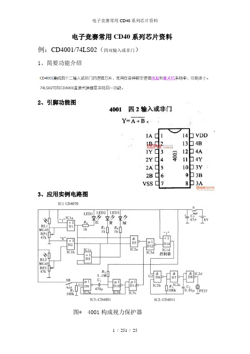
例:CD4001/74LS02(四双输入或非门)1、简要功能介绍2、引脚功能图3、应用实例电路图图* 4001构成视力保护器例:CD4011/74LS08(四2输入端与非门)1、引脚功能图逻辑表达式:Y = A.B(1)当X=0、Y=0时,将使两个NAND门之输出均为1,违反触发器之功用,故禁止使用。
如真值表第一列。
(2)当X=0、Y=1时,由于X=1导致NAND-A的输出为”1”,使得NAND-B的两个输入均为”1”,因此NAND-B的输出为”0”,如真值表第二列。
(3)当X=1、Y=0时,由于Y=0导致NAND-B的输出为”1”,使得NAND-1的两个输入均为””1,因此NAND-A的输出为”0”,如真值表第三列。
(4)当X=1、Y=1时,因为一个””1不影响NAND门的输出,所以两个NAND门的输出均不改变状态,如真值表第四列。
3、应用实例电路图例:CD4012/74LS20(双4输入端与非门)例:CD4017/CD4022(十进制计数/分配器)1、简要功能介绍CD4017 是5 位Johnson 计数器,具有10 个译码输出端,CP、CR、INH 输入端。
时钟输cd4017入端的斯密特触发器具有脉冲整形功能,对输入时钟脉冲上升和下降时间无限制。
INH 为低电平时,计数器在时钟上升沿计数;反之,计数功能无效。
CR 为高电平时,计数器清零。
2、引脚功能图CO:进位脉冲输出CP:时钟输入端CR:清除端INH:禁止端Q0-Q9 计数脉冲输出端VDD:正电源VSS:地3、应用实例电路图例:CD4026(十进制计数/7段译码器)1、引脚功能图当2和15为低3为高时,数码管随脉冲0-1-2…9-02脚为高电平时计数锁存脚5.4.14一般为高显9时5脚为低显2时14脚为低4脚与3脚一至3、应用实例电路图图* 4026构成时基电路例:CD4027/74LS111、114(双J-K触发器)1、引脚功能图当jk同时为1时Qn+1=Qn’3、应用实例电路图该振荡器能产生交变的50Hz脉冲方波,其占空比为50%。
CD系列门电路

CD4000 双3输入端或非门CD4001 四2输入端或非门CD4002 双4输入端或非门CD4007 双互补对加反向器CD4009 六反向缓冲/变换器CD4011 四2输入端与非门CD4012 双4输入端与非门CD4023 三2输入端与非门CD4025 三2输入端与非门CD4030 四2输入端异或门CD4041 四同相/反向缓冲器CD4048 8输入端可扩展多功能门CD4049 六反相缓冲/变换器CD4050 六同相缓冲/变换器CD4068 8输入端与门/与非门CD4069 六反相器CD4070 四2输入异或门CD4071 四2输入端或门CD4072 双4输入端或门CD4073 三3输入端与门CD4075 三3输入端或门CD4077 四异或非门CD4078 8输入端与非门/或门CD4081 四2输入端与门CD4082 双4输入端与非门CD4085 双2路2输入端与或非门CD4086 四2输入端可扩展与或非门CD40104 TTL至高电平CMOS转换器CD40106 六施密特触发器CD40107 双2输入端与非缓冲/驱动器CD40109 四低-高电平位移器CD4501 三多输入门CD4052 六反向缓冲器(三态输出)CD4503 六同相缓冲器(三态输出)CD4504 6TTL或CMOS同级移相器CD4506 双可扩展AIO门CD4507 四异或门CD4519 4位与/或选择器CD4530 双5输入多数逻辑门CD4572 四反向器加二输入或非门加二输入与非门CD4599 8位可寻址锁存器*************************************************** 触发器CD4013 双D触发器CD4042 四锁存D型触发器CD4043 四三态R-S锁存触发器(“1”触发)CD4044 四三态R-S锁存触发器(“0”触发)CD4047 单稳态触发/无稳多谐振荡器CD4093 四2输入端施密特触发器CD4098 双单稳态触发器CD4099 8位可寻址锁存器CD4508 双4位锁存触发器CD4528 双单稳态触发器(与CD4098管脚相同,只是3、13脚复位开关为高电平有效)CD4538 精密单稳多谐振荡器CD4583 双施密特触发器CD4584 六施密特触发器CD4599 8位可寻址锁存器***************************************************计数器CD4017 十进制计数/分配器CD4020 14位二进制串行计数器/分频器CD4022 八进制计数/分配器CD4024 7位二进制串行计数器/分频器CD4029 可预置数可逆计数器(4位二进制或BCD码)CD4040 12二进制串行计数器/分频器CD4045 12位计数/缓冲器CD4059 四十进制N分频器CD4060 14二进制串行计数器/分频器和振荡器CD4095 3输入端J-K触发器(相同J-K输入端)CD4096 3输入端J-K触发器(相反和相同J-K输入端)CD40110 十进制加/减计数/锁存/7端译码/驱动器CD40160 可预置数BCD加计数器(异步复位)CD40161 可预置数4位二进制加计数器(R非=0时,CP上脉冲复位)(异步复位)CD40162 可预置数BCD加计数器(同步复位)CD40163 可预置数4位二进制加计数器(R非=0时,CP上脉冲复位)(同步复位)CD40192 可预置数BCD加/减计数器CD40193 可预置数4位二进制加/减计数器CD4510 可预置BCD加/减计数器CD4516 可预置4位二进制加/减计数器CD4518 双BCD同步加计数器CD4520 双同步4位二进制加计数器CD4521 24级频率分频器CD4522 可预置数BCD同步1/N加计数器CD4526 可预置数4位二进制同步1/N加计数器CD4534 实时与译码计数器CD4536 可编程定时器CD4553 3数字BCD计数器CD4568 相位比较器/可编程计数器CD4569 双可预置BCD/二进制计数器CD4597 8位总线相容计数/锁存器CD4598 8位总线相容可建地址锁存器***************************************************译码器CD4511 BCD锁存/7段译码器/驱动器CD4514 4位锁存/4-16线译码器CD4515 4位锁存/4-16线译码器(负逻辑输出)CD4026 十进制计数/7段译码器(适用于时钟计时电路,利用C端的功能可方便的实现60或12分频)CD4028 BCD-十进制译码器CD4033 十进制计数/7段译码器CD4054 4位液晶显示驱动CD4055 BCD-7段码/液晶驱动CD4056 BCD-7段码/驱动CD40102 8位可预置同步减法计时器(BCD)CD40103 8位可预置同步减法计时器(二进制)CD4513 BCD-锁存/7端译码/驱动器(无效“0”不显)CD4514 4位锁存/4线—16线译码器(输出“1”)CD4515 4位锁存/4线—16线译码器(输出“0”)CD4543 BCD-锁存/7段译码/驱动器CD4544 BCD-锁存/7段译码/驱动器——波动闭锁CD4547 BCD-锁存/7段译码/大电流驱动器CD4555 双二进制4选1译码器/分离器(输出“1”)CD4556 双二进制4选1译码器/分离器(输出“0”)CD4558 BCD-7段译码CD4555 双二进制4选1译码器/分离器CD4556 双二进制4选1译码器/分离器(负逻辑输出)***************************************************移位寄存器CD4006 18位串入—串出移位寄存器CD4014 8位串入/并入—串出移位寄存器CD4015 双4位串入—并出移位寄存器CD4021 8位串入/并入—串出移位寄存器CD4031 64位移位寄存器CD4034 8位通用总线寄存器CD4035 4位串入/并入—串出/并出移位寄存器CD4076 4线D型寄存器CD4094 8位移位/存储总线寄存器CD40100 32位左移/右移CD40105 先进先出寄存器CD40108 4×4多端口寄存器阵列CD40194 4位并入/串入—并出/串出移位寄存器(左移/右移)CD40195 4位并入/串入—并出/串出移位寄存器CD4517 64位移位寄存器CD45490 连续的近似值寄存器CD4562 128位静态移位寄存器CD4580 4×4多端寄存器***************************************************模拟开关和数据选择器CD4016 四联双向开关CD4019 四与或选择器【Qn=(An*Ka)+(Bn*Kb)】CD4051 单八路模拟开关CD4052 双4路模拟开关CD4053 三2路模拟开关CD4066 四双向模拟开关CD4067 单十六路模拟开关CD4097 双八路模拟开关CD40257 四2选1数据选择器CD4512 八路数据选择器CD4529 双四路/单八路模拟开关CD4539 双四路数据选择器CD4551 四2通道模拟多路传输***************************************************运算电路CD4008 4位超前进位全加器CD4019 四与或选择器【Qn=(An*Ka)+(Bn*Kb)】CD4527 BCD比例乘法器CD4032 三路串联加法器CD4038 三路串联加法器(负逻辑)CD4063 四位量级比较器CD4070 四2输入异或门CD4585 4位数值比较器CD4089 4位二进制比例乘法器CD40101 9位奇偶发生器/校验器CD4527 BCD比例乘法器CD4531 12位奇偶数CD4559 逐次近似值码器CD4560 “N”BCD加法器CD4561 “9”求补器CD4581 4位算术逻辑单元CD4582 超前进位发生器CD4585 4位数值比较器***************************************************存储器CD4049 4字×8位随机存取存储器CD4505 64×1位RAMCD4537 256×1静态随机存取存储器CD4552 256位RAM*************************************************** 特殊电路CD4046 锁相环集成电路CD4532 8位优先编码器CD4500 工业控制单元CD4566 工业时基发生器CD4573 可预置运算放大器CD4574 比较器、线性、双对双运放CD4575 双/双预置运放/比较器CD4597 8位总线相容计数/锁存器CD4598 8位总线相容可建地址锁存器。
CD4000系列芯片功能

CD4000系列芯片功能CD4000系列芯片是一系列CMOS数字集成电路,主要用途是实现数字逻辑电路和模拟电路之间的转换。
这个系列的芯片包含了很多不同的功能,每个芯片都有各自特定的功能和用途。
以下是CD4000系列芯片的一些主要功能。
1.CD4001:四两输入与非门。
该芯片包含了四个两输入与非门,可用于构建逻辑电路、计算器和时序电路等。
2.CD4002:双四输入与非门。
该芯片包含了两个四输入与非门,可以用于构建更复杂的逻辑电路。
3.CD4008:八位加法器。
该芯片是一个八位全加器,可以用于进行数值计算、逻辑判断和算术操作等。
4.CD4011:四两输入与门。
该芯片包含了四个两输入与门,可以用于构建逻辑门电路和数字逻辑电路等。
5.CD4013:双D触发器。
该芯片包含了两个D触发器,可以用于存储和延时操作等。
6.CD4017:十译码器/分频器。
该芯片是一个十译码器和分频器,可以用于驱动LED显示、设计计数器和时钟电路等。
7.CD4026:十位数码计数器。
该芯片是一个十进制数码计数器,可以用于设计计时器和数字显示器等。
8.CD4040:二十四位二进制计数器。
该芯片是一个二十四位二进制计数器,可以用于设计时序电路、频率分频器和计时器等。
9.CD4060:二进制十二位倒计数器/分频器。
该芯片是一个二进制十二位倒计数器和分频器,可以用于设计计时器、时钟电路和频率计数器等。
10.CD4071:四两输入或门。
该芯片包含了四个两输入或门,可以用于构建逻辑电路和数字逻辑电路等。
总之,CD4000系列芯片具有很多不同的功能,涵盖了逻辑门、触发器、计数器、分频器等多种数字电路的应用。
这些芯片通常以低功耗、高稳定性和高抗干扰性能而闻名,并且在电子设备和嵌入式系统中被广泛使用。
常用CD系列门电路

常用CD系列门电路2006年04月17日 21:180 [导读] 门电路 CD4000 双3输入端或非门CD4001 四2输入端或非门
*CD4002 双4输入端或非门CD4007 双互补对入端或非门
CD40
01 四2输入端或非门 *CD4002 双4输入端或非门CD4007 双 互补对加反向器CD4009 六反向缓冲/变换器CD4011
端与非缓冲/驱动器CD40109 四低-高电平位移器CD4501 三多输入门CD4052 六反向缓冲器(三态输出)*CD4503 六
cd4012

CC4012------双4输入与非门简要说明CC4011为4输入正向逻辑与非门。
CC4011与非门为系统设计者提供了直接的与非功能,补充了已有COS/MOS 门系列,所有输入和输出经过缓冲,改善了输入/输出传输特性,使得由于负载容量的增加而引起的传输时间的变化维持到最小。
CC4011提供了14引线多层陶瓷双列直插(D)、熔封陶瓷双列直插(J)、塑料双列直插(P)和陶瓷片状载体(C)4种封装形式。
引出端符号1A-2A,1B-2B,1C-2C,1D-2D输入端1Y-2Y 输出端V DD正电源Vss 地推荐工作条件电源电压范围…………3V~15V输入电压范围…………0V~V DD工作温度范围M类…………-55℃~125℃E类………….-40℃~85℃极限值电源电压…...-0.5V~18V输入电压……-0.5V~V DD+0.5V输入电流…………….±10mA储存稳定…………-65℃~150℃逻辑符号引出端排列(俯视)逻辑图(1/2)逻辑表达式静态特性:测试条件规范值参数V O (V)V I(V)V DD(V)-55℃-40℃ 25℃ 85℃ 125℃单位V OL输出低电平电压(最大)- 5/010/015/05.010.015.00.05 VV OH输出高电平电压(最小)- 5/010/015/05.010.015.04.959.9514.95VV IL输入低电平电压(最大)4.59.013.5- 5.010.015.01.53.04.0VV IH输入高电平电压(最小)4.5/0.59.0/1.013.5/1.5- 5.010.015.03.57.011.0VI OH输出高电平电流(最小)2.54.69.513.55/05/010/015/05.05.010.015.0-2.0-0.64-1.6-4.2-1.8-0.61-1.5-4.0-1.6-0.51-1.3-3.4-1.3-0.42-1.1-2.8-1.15-0.36- 0.9-2.4mAI OL输出低电平电流(最小)0.40.51.55/010/015/05.010.015.00.641.64.20.611.54.00.511.33.40.421.12.80.360.92.4mAI I输入电流- 15/015.0±0.1 ±1.0 µAI DD电源电流(最大)- 5/010/015/05.010.015.00.250.51.00.250.51.07.515.030.0µA动态特性(TA=25℃):规范值参数测试条件V DD(V)最小最大单位t PLH输出由低电平到高电平传输延迟时间5.010.015.0- 25012090nst PHL输出由高电平到低电平传输延迟时间5.010.015.0- 25012090nst TLH输出由低电平到高电平转换时间5.010.015.0- 20010080nst THL输出由高电平到低电平转换时间5.010.015.0- 20010080nsC I输入电容(任一输入端)C L=50pFR L=200kt r=20nst f=20ns- - 7.5 pF。
CD系列门电路

CD系列门电路CD4000 双3输入端或非门CD4001 四2输入端或非门CD4002 双4输入端或非门CD4007 双互补对加反向器CD4009 六反向缓冲/变换器CD4011 四2输入端与非门CD4012 双4输入端与非门CD4023 三2输入端与非门CD4025 三2输入端与非门CD4030 四2输入端异或门CD4041 四同相/反向缓冲器CD4048 8输入端可扩展多功能门CD4049 六反相缓冲/变换器CD4050 六同相缓冲/变换器CD4068 8输入端与门/与非门CD4069 六反相器CD4070 四2输入异或门CD4071 四2输入端或门CD4072 双4输入端或门CD4073 三3输入端与门CD4075 三3输入端或门CD4077 四异或非门CD4078 8输入端与非门/或门CD4081 四2输入端与门CD4082 双4输入端与非门CD4085 双2路2输入端与或非门CD4086 四2输入端可扩展与或非门CD40104 TTL至高电平CMOS转换器CD40106 六施密特触发器CD40107 双2输入端与非缓冲/驱动器CD40109 四低-高电平位移器CD4501 三多输入门CD4052 六反向缓冲器(三态输出)CD4503 六同相缓冲器(三态输出)CD4504 6TTL或CMOS同级移相器CD4506 双可扩展AIO门CD4507 四异或门CD4519 4位与/或选择器CD4530 双5输入多数逻辑门CD4572 四反向器加二输入或非门加二输入与非门CD4599 8位可寻址锁存器*************************************************** 触发器CD4013 双D触发器CD4042 四锁存D型触发器CD4043 四三态R-S锁存触发器(“1”触发)CD4044 四三态R-S锁存触发器(“0”触发)CD4047 单稳态触发/无稳多谐振荡器CD4093 四2输入端施密特触发器CD4098 双单稳态触发器CD4099 8位可寻址锁存器CD4508 双4位锁存触发器CD4528 双单稳态触发器(与CD4098管脚相同,只是3、13脚复位开关为高电平有效)CD4538 精密单稳多谐振荡器CD4583 双施密特触发器CD4584 六施密特触发器CD4599 8位可寻址锁存器***************************************************计数器CD4017 十进制计数/分配器CD4020 14位二进制串行计数器/分频器CD4022 八进制计数/分配器CD4024 7位二进制串行计数器/分频器CD4029 可预置数可逆计数器(4位二进制或BCD码)CD4040 12二进制串行计数器/分频器CD4045 12位计数/缓冲器CD4059 四十进制N分频器CD4060 14二进制串行计数器/分频器和振荡器CD4095 3输入端J-K触发器(相同J-K输入端)CD4096 3输入端J-K触发器(相反和相同J-K输入端)CD40110 十进制加/减计数/锁存/7端译码/驱动器CD40160 可预置数BCD加计数器(异步复位)CD40161 可预置数4位二进制加计数器(R非=0时,CP上脉冲复位)(异步复位)CD40162 可预置数BCD加计数器(同步复位)CD40163 可预置数4位二进制加计数器(R非=0时,CP上脉冲复位)(同步复位)CD40192 可预置数BCD加/减计数器CD40193 可预置数4位二进制加/减计数器CD4510 可预置BCD加/减计数器CD4516 可预置4位二进制加/减计数器CD4518 双BCD同步加计数器CD4520 双同步4位二进制加计数器CD4521 24级频率分频器CD4522 可预置数BCD同步1/N加计数器CD4526 可预置数4位二进制同步1/N加计数器CD4534 实时与译码计数器CD4536 可编程定时器CD4553 3数字BCD计数器CD4568 相位比较器/可编程计数器CD4569 双可预置BCD/二进制计数器CD4597 8位总线相容计数/锁存器CD4598 8位总线相容可建地址锁存器***************************************************译码器CD4511 BCD锁存/7段译码器/驱动器CD4514 4位锁存/4-16线译码器CD4515 4位锁存/4-16线译码器(负逻辑输出)CD4026 十进制计数/7段译码器(适用于时钟计时电路,利用C 端的功能可方便的实现60或12分频)CD4028 BCD-十进制译码器CD4033 十进制计数/7段译码器CD4054 4位液晶显示驱动CD4055 BCD-7段码/液晶驱动CD4056 BCD-7段码/驱动CD40102 8位可预置同步减法计时器(BCD)CD40103 8位可预置同步减法计时器(二进制)CD4513 BCD-锁存/7端译码/驱动器(无效“0”不显)CD4514 4位锁存/4线—16线译码器(输出“1”)CD4515 4位锁存/4线—16线译码器(输出“0”)CD4543 BCD-锁存/7段译码/驱动器CD4544 BCD-锁存/7段译码/驱动器——波动闭锁CD4547 BCD-锁存/7段译码/大电流驱动器CD4555 双二进制4选1译码器/分离器(输出“1”)CD4556 双二进制4选1译码器/分离器(输出“0”)CD4558 BCD-7段译码CD4555 双二进制4选1译码器/分离器CD4556 双二进制4选1译码器/分离器(负逻辑输出)***************************************************移位寄存器CD4006 18位串入—串出移位寄存器CD4014 8位串入/并入—串出移位寄存器CD4015 双4位串入—并出移位寄存器CD4021 8位串入/并入—串出移位寄存器CD4031 64位移位寄存器CD4034 8位通用总线寄存器CD4035 4位串入/并入—串出/并出移位寄存器CD4076 4线D型寄存器CD4094 8位移位/存储总线寄存器CD40100 32位左移/右移CD40105 先进先出寄存器CD40108 4×4多端口寄存器阵列CD40194 4位并入/串入—并出/串出移位寄存器(左移/右移)CD40195 4位并入/串入—并出/串出移位寄存器CD4517 64位移位寄存器CD45490 连续的近似值寄存器CD4562 128位静态移位寄存器CD4580 4×4多端寄存器***************************************************模拟开关和数据选择器CD4016 四联双向开关CD4019 四与或选择器【Qn=(An*Ka)+(Bn*Kb)】CD4051 单八路模拟开关CD4052 双4路模拟开关CD4053 三2路模拟开关CD4066 四双向模拟开关CD4067 单十六路模拟开关CD4097 双八路模拟开关CD40257 四2选1数据选择器CD4512 八路数据选择器CD4529 双四路/单八路模拟开关CD4539 双四路数据选择器CD4551 四2通道模拟多路传输***************************************************运算电路CD4008 4位超前进位全加器CD4019 四与或选择器【Qn=(An*Ka)+(Bn*Kb)】CD4527 BCD比例乘法器CD4032 三路串联加法器CD4038 三路串联加法器(负逻辑)CD4063 四位量级比较器CD4070 四2输入异或门CD4585 4位数值比较器CD4089 4位二进制比例乘法器CD40101 9位奇偶发生器/校验器CD4527 BCD比例乘法器CD4531 12位奇偶数CD4559 逐次近似值码器CD4560 “N”BCD加法器CD4561 “9”求补器CD4581 4位算术逻辑单元CD4582 超前进位发生器CD4585 4位数值比较器***************************************************存储器CD4049 4字×8位随机存取存储器CD4505 64×1位RAMCD4537 256×1静态随机存取存储器CD4552 256位RAM*************************************************** 特殊电路CD4046 锁相环集成电路CD4532 8位优先编码器CD4500 工业控制单元CD4566 工业时基发生器CD4573 可预置运算放大器CD4574 比较器、线性、双对双运放CD4575 双/双预置运放/比较器CD4597 8位总线相容计数/锁存器CD4598 8位总线相容可建地址锁存器。
- 1、下载文档前请自行甄别文档内容的完整性,平台不提供额外的编辑、内容补充、找答案等附加服务。
- 2、"仅部分预览"的文档,不可在线预览部分如存在完整性等问题,可反馈申请退款(可完整预览的文档不适用该条件!)。
- 3、如文档侵犯您的权益,请联系客服反馈,我们会尽快为您处理(人工客服工作时间:9:00-18:30)。
TL F 5940CD4002M CD4002C Dual 4-Input NOR Gate CD4012M CD4012C Dual 4-Input NAND GateMarch 1988CD4002M CD4002C Dual 4-Input NOR Gate CD4012M CD4012C Dual 4-Input NAND GateGeneral DescriptionThese NOR and NAND gates are monolithic complementa-ry MOS (CMOS)integrated circuits The N-and P-channel enhancement mode transistors provide a symmetrical cir-cuit with output swings essentially equal to the supply volt-age This results in high noise immunity over a wide supply voltage range No DC power other than that caused by leak-age current is consumed during static conditions All inputs are protected against static discharge and latching condi-tionsFeaturesY Wide supply voltage range 3 0V to 15V Y Low power10nW (typ )YHigh noise immunity0 45V DD (typ )ApplicationsY Automotive Y Alarm system Y Data terminals Y Industrial controls Y Instrumentation Y Remote metering YMedical ElectronicsYComputersConnection DiagramsCD4002Dual-In-Line PackageTL F 5940–1Top ViewCD4012Dual-In-Line PackageTL F 5940–2Top ViewOrder Number CD4002or CD4012C 1995National Semiconductor Corporation RRD-B30M105 Printed in U S AAbsolute Maximum Ratings(Note1)If Military Aerospace specified devices are required please contact the National Semiconductor Sales Office Distributors for availability and specifications Voltage at Any Pin V SS b0 3V to V DD a0 3V Operating Temperature RangeCD4002M CD4012M b55 C to a125 C CD4002C CD4012C b40 C to a85 C Storage Temperature Range(T S)b65 C to a150 C Power Dissipation(P D)Dual-In-Line700mW Small Outline500mW Operating Range(V DD)V SS a3 0V to V SS a15V Lead Temperature(T L)(Soldering 10seconds)260 CDC Electrical Characteristics CD4002M CD4012MLimitsSymbol Parameter Conditions b55 C a25 C a125 C UnitsMin Max Min Typ Max Min MaxI DD Quiescent V DD e5 0V0 050 0010 053 0m ADevice Current V DD e10V0 10 0010 16m A P D Quiescent Device V DD e5 0V0 250 0050 2515m W Dissipation Package V DD e10V1 00 011 060m W V OL Output Voltage V DD e5 0V V I e V DD I O e0A0 0500 050 05V Low Level V DD e10V V I e V DD I O e0A0 0500 050 05V V OH Output Voltage V DD e5 0V V I e V SS I O e0A4 954 955 04 95V High Level V DD e10V V I e V SS I O e0A9 959 95109 95V V NL Noise Immunity V DD e5 0V V O e3 6V I O e0A1 51 52 251 4V (All Inputs)V DD e10V V O e7 2V I O e0A3 03 04 52 9V V NH Noise Immunity V DD e5 0V V O e0 95V I O e0A1 41 52 251 5V (All Inputs)V DD e10V V O e2 9V I O e0A2 93 04 53 0V I D N Output Drive Current V DD e5 0V V O e0 4V V I e V DD0 50 401 00 28mAN-Channel(4002)V DD e10V V O e0 5V V I e V DD1 10 92 50 65mA (Note2)I D P Output Drive Current V DD e5 0V V O e2 5V V I e V SS b0 62b0 5b2 0b0 35mAP-Channel(4002)V DD e10V V O e9 5V V I e V SS b0 62b0 5b1 0b0 35mA (Note2)I D N Output Drive Current V DD e5 0V V O e0 4V V I e V DD0 310 250 50 175mAN-Channel(4012)V DD e10V V O e0 5V V I e V DD0 630 50 60 35mA (Note2)I D P Output Drive Current V DD e5 0V V O e2 5V V I e V SS b0 31b0 25b0 5b0 175mAP-Channel(4012)V DD e10V V O e9 5V V I e V SS b0 75b0 6b1 2b0 4mA (Note2)I I Input Current10pANote1 ‘‘Absolute Maximum Ratings’’are those values beyond which the safety of the device cannot be guaranteed Except for‘‘Operating Temperature Range’’they are not meant to imply that the devices should be operated at these limits The table of‘‘Electrical Characteristics’’provides conditions for actual device operationNote2 I D N and I D P are tested one output at a time2DC Electrical Characteristics CD4002C CD4012CLimitsSymbol Parameter Conditions b55 C a25 C a85 C UnitsMin Max Min Typ Max Min MaxI DD Quiescent V DD e5 0V0 50 0050 515m ADevice Current V DD e10V5 00 0055 030m A P D Quiescent Device V DD e5 0V2 50 0252 575m W Dissipation Package V DD e10V500 0550300m W V OL Output Voltage V DD e5 0V V I e V DD I O e0A0 0500 050 05V Low Level V DD e10V V I e V DD I O e0A0 0500 050 05V V OH Output Voltage V DD e5 0V V I e V SS I O e0A4 954 955 04 95V High Level V DD e10V V I e V SS I O e0A9 959 95109 95V V NL Noise Immunity V DD e5 0V V O t3 6V I O e0A1 51 52 251 4V (All Inputs)V DD e10V V O t7 2V I O e0A3 03 04 52 9V V NH Noise Immunity V DD e5 0V V O s0 95V I O e0A1 41 52 251 5V (All Inputs)V DD e10V V O s2 9V I O e0A2 93 04 53 0V I D N Output Drive Current V DD e5 0V V O e0 4V V I e V DD0 350 31 00 24mAN-Channel(4002)V DD e10V V O e0 5V V I e V DD0 720 62 50 48mA (Note2)I D N Output Drive Current V DD e5 0V V O e0 4V V I e V DD0 1450 120 50 095mAN-Channel(4012)V DD e10V V O e0 5V V I e V DD0 30 250 60 2mA (Note2)I D P Output Drive Current V DD e5 0V V O e2 5V V I e V SS b0 35b0 3b2 0b0 24mAP-Channel(4002)V DD e10V V O e9 5V V I e V SS b0 3b0 25b1 0b0 2mA (Note2)I D P Output Drive Current V DD e5 0V V O e2 5V V I e V SS b0 145b0 12b0 5b0 095mAP-Channel(4012)V DD e10V V O e9 5V V I e V SS b0 35b0 3b1 2b0 24mA (Note2)I I Input Current10pANote1 ‘‘Absolute Maximum Ratings’’are those values beyond which the safety of the device cannot be guaranteed Except for‘‘Operating Temperature Range’’they are not meant to imply that the devices should be operated at these limits The table of‘‘Electrical Characteristics’’provides conditions for actual device operationNote2 I D N and I D P are tested one output at a time3AC Electrical Characteristics T A e25 C C L e15pF and input rise and fall times e20ns Typical temperature coefficient for all values of V DD e0 3% CSymbol Parameter Conditions Min Typ Max Units CD4002Mt PHL Propagation Delay Time V DD e5 0V3550ns High to Low Level V DD e10V2540ns t PLH Propagation Delay Time V DD e5 0V3550ns Low to High Level V DD e10V2540ns t THL Transition Time High V DD e5 0V65175ns to Low Level V DD e10V3575ns t TLH Transition Time Low V DD e5 0V65125ns to High Level V DD e10V3570nsC IN Input Capacitance Any Input5 0pFCD4002Ct PHL Propagation Delay Time V DD e5 0V35120ns High to Low Level V DD e10V2565ns T PLH Propagation Delay Time V DD e5 0V3580ns Low to High Level V DD e10V2555ns t THL Transition Time High V DD e5 0V65300ns to Low Level V DD e10V35125ns t TLH Transition Time Low V DD e5 0V65200ns to High Level V DD e10V35115nsC IN Input Capacitance Any Input5 0pFAC Parameters are guaranteed by DC correlated testingAC Electrical Characteristics T A e25 C C L e15pF and input rise and fall times e20ns Typical temperature coefficient for all values of V DD e0 3% CSymbol Parameter Conditions Min Typ Max Units CD4012Mt PHL Propagation Delay Time V DD e5 0V5075ns High to Low Level V DD e10V2540ns t PLH Propagation Delay Time V DD e5 0V5075ns Low to High Level V DD e10V2540ns t THL Transition Time High V DD e5 0V75125ns to Low Level V DD e10V5075ns t TLH Transition Time Low V DD e5 0V75100ns to High Level V DD e10V4060nsC IN Input Capacitance Any Input5 0pFCD4012Ct PHL Propagation Delay Time V DD e5 0V50100ns High to Low Level V DD e10V2550ns T PLH Propagation Delay Time V DD e5 0V50100ns Low to High Level V DD e10V2550ns t THL Transition Time High V DD e5 0V75150ns to Low Level V DD e10V50100ns t TLH Transition Time Low V DD e5 0V75125ns to High Level V DD e10V4075nsC IN Input Capacitance Any Input5 0pFAC Parameters are guaranteed by DC correlated testingNote1 ‘‘Absolute Maximum Ratings’’are those values beyond which the safety of the device cannot be guaranteed Except for‘‘Operating Temperature Range’’they are not meant to imply that the devices should be operated at these limits The table of‘‘Electrical Characteristics’’provides conditions for actual device operation4Physical Dimensions inches(millimeters)Ceramic Dual-In-Line Package(J)Order Number CD4002MJ CD4002CJ CD4012MJ or CD4012CJNS Package Number J14A5C D 4002M C D 4002C D u a l 4-I n p u t N O R G a t e C D 4012M C D 4012C D u a l 4-I n p u t N A N D G a t ePhysical Dimensions inches (millimeters)(Continued)Molded Dual-In-Line Package (N)Order Number CD4002MN CD4002CN CD4012MN or CD4012CNNS Package Number N14ALIFE SUPPORT POLICYNATIONAL’S PRODUCTS ARE NOT AUTHORIZED FOR USE AS CRITICAL COMPONENTS IN LIFE SUPPORT DEVICES OR SYSTEMS WITHOUT THE EXPRESS WRITTEN APPROVAL OF THE PRESIDENT OF NATIONAL SEMICONDUCTOR CORPORATION As used herein 1 Life support devices or systems are devices or 2 A critical component is any component of a life systems which (a)are intended for surgical implant support device or system whose failure to perform can into the body or (b)support or sustain life and whose be reasonably expected to cause the failure of the life failure to perform when properly used in accordance support device or system or to affect its safety or with instructions for use provided in the labeling can effectivenessbe reasonably expected to result in a significant injury to the userNational Semiconductor National Semiconductor National Semiconductor National Semiconductor CorporationEuropeHong Kong LtdJapan Ltd1111West Bardin RoadFax (a 49)0-180-530858613th Floor Straight Block Tel 81-043-299-2309。