3288四核安卓板规格书V1.0(2)
RK3288硬件参数解读

性能提升50%!最新ARM神秘内核RK3288硬件参数解读在拉斯维加斯CES 2014 上,瑞芯微带来全新的RK3288处理器:“全球第一个四核ARM 全新内核芯片、全球第一个支持最新超强Mali-T76x系列GPU的芯片以及全球第一个4Kx2K 硬解H.265的芯片”而被业界关注。
平板知名OEM厂商包括原道、五元素、驰为等纷纷跟随新品蓄势待发。
本文将从硬件参数对RK3288进行解读,看看参数背后代表了什么意义。
一、RK3288采用全新ARM内核架构目前市场上的四核ARM处理器基本采用A9核心或A7核心,ARM也将在新年发布其最新架构内核,该全新架构,采用与Cortex-A15一样的乱序执行架构,最立竿见影的效果就是性能提升。
同时相比Cortex-A9更长的管线设计,频率也随之成倍提高使得RK3288的默认频率直达1.8GHz。
此外,双指令译码、双地址产生器(AGU)、多指令派发等特别架构的设计,使得采用全新架构的RK3288在指令执行效率上也有相当大的提升。
正是基于以上改进,在同样的频率下,新架构的单线程性能要比Cortex-A9有40%的提升;而频率高达1.8GHz的RK3288性能较上一代RK3188有50%的性能提升,性能大大优于八核A7处理器。
当然,在成熟的28nm 先进制造工艺的保驾护航下,RK3288的功耗甚至比四核A9还要低。
二、RK3288采用最强移动GPU,性能媲美桌面GPURK3288所采用的GPU让人非常震撼——最新、最强的Mali T76X核心! Mali T76X 是ARM最新Mali T700系列GPU最强的型号,拥有16个着色器核心,性能直逼桌面显卡。
以RK3288所采用的Mali T764核心为例,性能高达性能高达82 GFLOPS、2400M pixel/s,性能比Mali-T604GPU提升400%,而比目前市场主流的Mali-400MP4整整提升了500%,绝对是最快的移动GPU。
产品资料说明手册RK3288W V1.0硬件规格书V1.0_20170306 - 副本

RK3288W V1.0
数字标牌
规格书
文档修改历史
目录
第一章产品概述 (3)
1.1概述 (3)
1.2特点 (3)
1.3外观及接口示意图 (4)
第二章基本功能列表 (5)
第三章PCB尺寸和接口布局 (7)
3.1PCB尺寸图 (7)
3.2接口参数说明 (8)
第四章电气性能 (19)
第五章组装使用注意事项 (20)
第一章产品概述
1.1 概述
RK3288W V1.0板卡集成多媒体解码、液晶驱动、以太网、HDMI、WIFI、3G、蓝牙于一体,支持绝大部分当前流行的视频及图片格式解码,支持
HDMI视频输出/输入,双8/10位的LVDS接口以及eDP接口,可以驱
动各种TFT LCD显示屏,大大简化整机系统设计,SD卡和带锁的SIM
卡座,稳定性更强,非常适合于高清网络播放盒,视频广告机和画框广
告机.
1.2 特点
◆高集成度。
集成USB/LVDS/eDP/以太网/HDMI/WIFI/蓝牙于一体,
简化整机设计,可插SD卡.
◆内置PCI-E 3G模块.支持华为、中兴等多种PCI-E 3G/4G模块,更加适
合广告一体机的远程维护,节约人工成本.
◆丰富的扩展接口.7个USB接口(5个插针,2个标准USB口),4个可扩展
串口,GPIO/ADC接口,可以满足市场上各种外设的要求.
◆高清晰度。
最大支持3840x2160的解码和各种LVDS/eDP接口的LCD
显示屏.
◆功能齐全。
支持横竖屏播放,视频分屏,滚动字幕,定时开关,USB
数据导入等功能。
G3288开发板硬件手册说明书
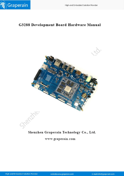
G3288Development Board Hardware ManualShenzhen Graperain Technology Co.,Ltd.Copyright StatementCopyrights of this manual belong to Shenzhen Graperain Technology Co.,Ltd.and all rights are reserved.Any companies or individuals are not allowed to extract part or all of this manual,and violators will be prosecuted under law.Attention:The manuals of development platform on sell will be updated from time to time,please download the latest manual from website or contact our company sales representative,there would be no further notice.Release NoteTechnical supportAny questions about the manuals,you can call our landline or email us. Website:Landline:+8675523025312E-mail:**********************Sales and service networkShenzhen Graperain Technology Co.,Ltd.Website:Landline:+8675523025312E-mail:*******************Address:Building D,Huafeng Tech.&Innov.Park Baoan Wisdom Valley,Xixiang,Baoan Dist.Shenzhen,Guangdong.Post code518101.CatalogueChapter1.G3288Development Board Brief (6)1.1G3288development board brief (6)1.2Characteristics Parameter (6)1.3G3288Development Board Appearance (8)1.4G3288SOM Appearance (8)Chapter2.G3288Development Board Hardware Resource (9)2.1G3288Development Board Hardware Resource Brief (9)2.2G3288SOM PIN Definition (10)Chapter3.Hardware Design (13)Chapter4.Product Portfolio (14)4.1System on Module Series (14)4.2Development Board Series (14)4.3Single Board Computer(SBC)Series (14)Chapter1.G3288Development Board Brief1.1G3288development board briefG3288development board takes Rockchip RK3288chip,designed by Shenzhen Graperain Technology Co.,Ltd..G3288development board includes G3288system on module and carrier board.G3288system on module takes Rockchip RK3288CPU,its dominant frequency about1.8GHz, integrated Mali-T760MP4graphic processor,it supports OpenGL ES1.1/2.0/3.0,OpenVG1.1, OpenCL,Directx11,and could come out4k x2K H.264and10bits H265video hardware decoding.G3288carrier board PIN out all functions of this chip mostly.Its data transmission and scalability have been extremely good play.Such as4G onboard,OTG,USB2.0,gigabit ethernet,dual band WIFI,bluetooth,audio input/output,multiple sensors,RGB,LVDS,MIPI,HDMI ect display interfaces and communication interfaces,camera and TF card slot.G3288development board supports Android,Linux,and Ubuntu OS,and all of them source code is open,which will be convenient to clients to develop.G3288module could be used in commercial display advertisement machine,vending machine, teaching terminal,automatic identification,robot,security monitoring,financial POS,vehicle control terminal,VR and so on directly,which will save time on developing well.G3288Development Board Characteristics:●Size:186.5mm x115.6mm●Strong functions,rich interfaces,and applicable widely●Supports Android5.1,Linux,Ubuntu OS,open source code and accelerate R&D cycle●Product stability and reliability1.2Characteristics Parameter1.3G3288Development Board AppearanceG3288Development Board Front View1.4G3288SOM AppearanceMore information of G3288SOM,please reference G3288System on module introduction.Chapter2.G3288Development Board Hardware Resource 2.1G3288Development Board Hardware Resource BriefNote:More information of G3288system on module,please reference G3288system on module introduction.Chapter3.Hardware Design3.1Design ReferenceTaking GR3288SOM as hardware platform,you could refer to power design,USB design,HDMI design,LVDS design,MIPI design,Audio design,Internet(Network card,WIFI,Bluetooth)design, camera design,and so on.These are open to customers,can refer to our carrier board design.Chapter4.Product Portfolio4.1System on Module SeriesG4418SOM(Samsung S5P4418)G6818SOM(Samsung S5P6818)G3288SOM(Rockchip RK3288)M9SOM(Qualcomm8916)4.2Development Board SeriesG4418development board(Samsung S5P4418)G6818development board(Samsung S5P6818)G3288development board(Rockchip RK3288)M9development board(Qualcomm8916)4.3Single Board Computer(SBC)SeriesG4418single board computer(Samsung S5P4418)G6818single board computer(Samsung S5P6818)G3288single board computer(Rockchip RK3288)Instructions:More information of specifications and other products,please pay attention to website and contact us directly.。
[BOM]RK3288_POPMETAL BOARD_V20_20141030
![[BOM]RK3288_POPMETAL BOARD_V20_20141030](https://img.taocdn.com/s3/m/e3b0054f804d2b160b4ec0ac.png)
光纤接口 二极管 钽电容 ESD
33 34 35 36 37 38 39 40 41 42 43 44 45 46 47 48 49 50 51 52 53 54 55 56 57 58 59 60 61 62 63 64
ESD
ESD Component,5V,0.5P,SMD,0410K 1/16W 5% ROHS CHIP RES 15K 1/16W 5% RES,thick film,47KOhm,+/-5%,1/16W,SMD0402 ROHS CHIP RES 510R 1/16W 5% RES,thick film,1.5KOhm,+/-5%,1/16W,SMD0402 ROHS CHIP RES 27R 1/16W 5% ROHS CHIP RES 56R 1/16W 5% ROHS CHIP RES 220K 1/16W 5% RES,thick film,120K +/-5%,1/16W,SMD0402 RES,thick film,18KOhm,+/-5%,1/16W,SMD0402 ROHS CHIP RES 33R 1/16W 5% ROHS CHIP RES 1.5 Ohm 1/16W +/-5% ROHS CHIP RES 470 Ohm 1/16W +/-5% ROHS CHIP RES 4.7 Ohm1/4W +/-5% ROHS CHIP RES 330K 1/16W +/-5%
102 103 12pF 4.7uF 1pF 2.2uF 101 47pF/NC 8pF 33pF/NC 104 1uF 8pF 82pF/NC 0.22uF 180pF/NC 0.2pF 0.47uF DQT-003 BAT54S 1N5819 220uF/4V AZ5525-01F
qy-rk3288嵌入式主板硬件说明书
QY-RK3288 嵌入式主板硬件说明书版本号:V 2.02018年01月浙江启扬智能有限公司版权所有QIYANG TECHNOLOGY Co., LtdCopyright Reserved有任何技术问题或需要帮助,请联系:*********************** 第2页 共20页 购买产品,请联系销售:********************更多信息请访问: 版本更新记录有任何技术问题或需要帮助,请联系:*********************** 第3页 共20页 购买产品,请联系销售:********************目 录阅读前须知:本手册主要介绍该主板的硬件接口................................................................................................ 4 一、前言 . (4)1.1、公司简介: .............................................................................................................................................. 4 1.2、QY-RK3288主板的使用建议: ............................................................................................................. 4 二、系统组成 .. (5)2.1、概述 .......................................................................................................................................................... 5 2.2、主板资源 .................................................................................................................................................. 7 三、接口功能 .. (8)3.1、基本接口功用说明: .............................................................................................................................. 9 3.2、接口引脚定义 ........................................................................................................................................ 10 四、主板性能说明 ................................................................................................................................................. 17 五、尺寸结构图 ..................................................................................................................................................... 17 六、软件描述 ......................................................................................................................................................... 19 七、附注 .. (19)有任何技术问题或需要帮助,请联系:*********************** 第4页 共20页 购买产品,请联系销售:********************阅读前须知:本手册主要介绍该主板的硬件接口 一、前言1.1、公司简介:浙江启扬智能科技有限公司位于美丽的西子湖畔,是一家专业研发,生产,销售高性能,低功耗,低成本,小体积嵌入式计算机主板,提供嵌入式硬件解决方案的高新技术企业。
多普达A3288(htc G4 Tatto)中文说明书
使用设备前,请仔细阅读本手册本手册专门用于指导您使用手机的功能,以及标注了一些使用过程中的注意事项。
当您从包装盒中取出电池时,电池尚未充电。
设备充电时,请勿取出电池。
如您打开或擅改设备的外壳,产品保证即失效。
知识产权声明Copyright 2009 武汉多普达通讯有限公司(简称多普达),版权所有,并保留一切权利。
、 均为多普达商标。
蓝牙和蓝牙标志均为Bluetooth SIG,Inc.所拥有之商标。
II microSD为SD Card Association的商标。
Java、J2ME 和所有其它以 Java 为基础的商标均为 Sun Microsystems,Inc. 在美国地区和其它国家的商标或注册商标。
本手册中所提及的其他公司、产品和服务名称为其分别拥有者的商标、注册商标或服务标记。
多普达保留随时修改本文件之内容的权利,恕不事先通知。
未经多普达事前书面同意,不能以任何形式或任何方式复制或传送本文件的任何部份,不论为电子或机械方式,包括摄影、录像或储存于可存取的系统中,亦不能以任何形式翻译为任何语言。
免责条款对于预装或捆绑于本产品中的任何游戏、应用程序包括相应文件(以下简称软件),或通过本产品取得的视听资料、内容、服务以及相关文件资料,包括但不限于任何图像、照片、动画、录像、录音、音乐、文字,(以下简称服务)皆由相应软件/服务提供商(以下简称提供商)负责其合法、真实和准确,并由提供商保证不违反国家法律、法规、公共道德及侵犯任何第三方之合法权益。
提供商保证所提供软件和服务的质量以及用户资料等信息安全和网络安全。
对于本产品用户在安装/使用软件或者使用服务而发生的一切问题,或其它因使用前述软件或服务而造成的一切问题,包括因前述问题所产生之任何直接、间接、附带或因此而导致之衍生请仔细阅读III 性损失,概由相应提供商承担责任,皆与多普达无涉。
部分软件和服务需要网络支持,并可能需要支付相应费用。
限制赔偿依据现行法律允许的最大范围,任何情况下,多普达与其供应商不对使用者或第三方赔偿任何直接、间接、特殊、偶然的、无法避免的损害或损失,包括但不限于对在合约履行与侵权行为中可能发生的收入损失、信誉损失、商业机会损失、资料损失、利益损失、履行或不履行义务均不负责。
又一款RK3288板卡震撼来袭,四核A17处理器、主频1.8GHz,四核GPU
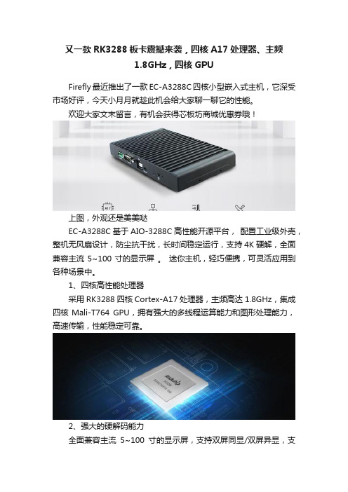
又一款RK3288板卡震撼来袭,四核A17处理器、主频
1.8GHz,四核GPU
Firefly最近推出了一款EC-A3288C四核小型嵌入式主机,它深受市场好评,今天小月月就趁此机会给大家聊一聊它的性能。
欢迎大家文末留言,有机会获得芯板坊商城优惠券哦!
上图,外观还是美美哒
EC-A3288C基于AIO-3288C高性能开源平台,配置工业级外壳,整机无风扇设计,防尘抗干扰,长时间稳定运行,支持4K硬解,全面兼容主流5~100寸的显示屏。
迷你主机,轻巧便携,可灵活应用到各种场景中。
1、四核高性能处理器
采用RK3288四核Cortex-A17处理器,主频高达1.8GHz,集成四核Mali-T764 GPU,拥有强大的多线程运算能力和图形处理能力,高速传输,性能稳定可靠。
2、强大的硬解码能力
全面兼容主流5~100寸的显示屏,支持双屏同显/双屏异显,支
持4K硬解,能实现4Kx2K的H.264和H.265视频硬解码,高清显示,感受不一样的视觉体验。
3、解码能力工业级应用性能
支持RS232(带硬件流控)及RS485接口,外型小巧便携,多种安装方式,隐蔽式引线孔,硅胶脚垫,方便快捷地连接各种工业设备。
4、无风扇高效散热
无风扇设计,铝合金结构导热,高效降温,防尘防震防干扰能力强,60℃高温老化,7x24小时稳定运行,满足工业级应用需求。
5、开放资料
提供配套的源代码、教程、技术资料和开发工具,让开发变得更加简单方便。
6、丰富的接口
拥有HDMI2.0、VGA、LAN、RS485、RS232等接口。
7、产品配置遥遥领先。
RK3288A CPU 四核 23.8 英寸 LCD 显示屏 充电及控制机柜说明书

23.8寸屏23.8 -inch screen产品规格表Item Specification各部件名称Component Name使用说明书25口机柜2主板型号(Mainboard Model):RK3288A CPU :RK3288, 四核(Quad-core),主频(mainfrequency) 1.8GHz,And roid 5.1.1Operating Instruction5 slots station注:机柜包装箱不含移动电源Note: The station packing case does not contain a power supply产品特点product feature本产品适合于公共场所及店铺中为客人提供共享充电服务的充电及控制机柜,产品正面23.8寸LCD 显示屏幕。
This product is suitable for charging and control cabinets thatprovide shared charging services for guests in public places and stores.The front of the product has a 23.8-inch LCD display screen. 扣手Handle喇叭trumpet23.8寸屏23.8 -inch 充电宝底座power bank产品名称productname 型号model尺寸size支持通讯communication support 机柜输入电压station input voltage机柜输入最大电流Maximum station input current机柜额定功率Rated cabinet power AC电源适配器输入AC power adapter input 螢幕机柜输出power outputscreen5V1.5A*25口100Vac-240Vac(60Hz/60Hz)1.31A(满载状态)/0.41A(待机状态)1.31A(full load) /0.41A(standby)530W(充电宝充电状态)(Charging status of the power bank)220V/50hz4G WIFI 2G 23.8英寸23.8-inch445mm(L)*600mm(W)*1780mm(H)23.8寸广告机23.8inch advertising machine YBT-107电源孔位指示灯轴视图Axis viewPower socket indicatorpedestal1.将AC电源线连接机柜背面的输入口。
RK3288(LX-RK3288-DDR3-V1.06)主板规格书-中性

LX-RK3288V1.06产品技术手册目录一、产品概述 (3)二、硬件特征 (4)三、端子描述(实物图) (5)四、接口定义 (6)1.连接器丝印位置图示: (6)2.引脚功能详细描叙: (7)五、结构 (15)六、运输、存储、使用条件 (15)七、物理尺寸 (16)一、产品概述主要功能瑞瑞芯微电子(Rockchip)推出的RK3288四核处理器,采用低漏电,高性能28nm HKMG工艺艺,ARM Cortex-A17四核架构,核心主频均可达1.8GHz,拥有1MB二级缓存;支持4K H.H.264和10bits H.265视频解码,1080P多格式视频解码,支持HDMI和及LVDS(双通道24BIT)输出双显,完美支持3840x2160分辨率;兼容MIPI接接口LCD液晶屏;图形系统:MaARM Mali-T764GPU,支持TE,ASTC,AFBC技术,支持OpenGL ES1.1/2.0/3.0,Open VG1.1,OpenCL,DirectX11。
内嵌高性能2D加速硬件;硬件安全系统,支持HDCP222.X;接口方面,可支持HDMI2.0和千兆以太网卡。
显著特性超强四核ARM Cortex-A17的RK3288四核处理器,主频高达1.8GH,1MB的L2Cache4K H.264和10bits H.265视频解码,1080P多格式视频解码;支持H.264,VP8和MVC;图像增强处理功能;硬件提升低功耗下显示图像效果。
内存标配2G Byte of64-bit wide DDR3@528MHz宽范围电源管理:支持9-15V以内(推荐12VDC)外部电源供电支持HDMI,双/单通道LVDS多格式高清视频输出接口;可以支持HDMI+LVDS双屏显示支持外部RTC功能:掉电记忆时间,支持设定24小时内任意时间段开关机,实现按日,周,月,年自动循环支持HP OUT,MIC IN及功放输出:6WX2支持USB2.0-6路接口(其中1路USB用作OTG,其它5路用作HOST),一路扩展MINI-PCIE 标准接口USB通讯的3G/LTE(4G)模块,兼容移动,联通,电信模块,一路扩展USB网卡支持SDIO接口WIFI及蓝牙V4.0支持10/100/1000M(RJ45)以太网,支持双网口支持4路RS232接口(两路两线串口,一路四线串口,一路两线调试串口)支持两路i2c接口插针板载一个TF卡槽及GPIO扩展插针预留1路SPI接口插针I2C接口电容触摸屏接口预留CAMEAR MIPI摄像头接口插座预留LCM MIPI显示屏接口插座预留EDP(4LINE/2LINE)高清显示接口插座支持双通道10BIT LVDS接口插针,可外扩VGA显示或RGB接口LCD支持PWM,DC电平调光支持3.3v/5v/12v液晶LCD屏电压切换支持重力传感器自动旋转屏幕支持红外遥控二、硬件特征CPU及存储单元CPU RK3288Quad core ARM Cortex A17四核,主频1.8GHz 视频解码器(GPU)ARM Mali-T764GPU支持OpenGL ES1.1/2.0/3.0,Open VG1.1,OpenCL,DirectX11;内嵌高性能2D加速硬件;支持4K H.264和10bits H.265视频解码,1080P多格式视频解码;内存2GByte of64-bit wide DDR3@528MHz存储EMMC/NAND FLASH8GB/16GB系统Android5.1.1、LINUX数据传输接口1X TF TF卡多媒体存储设备(Micro SD型连接器)(J8100)2x USB2.0HOST High-speed,480Mbps(USB A型连接器)(JUSB1,JUSB2)3X USB2.0HOSTHigh-speed,480Mbps(PH2.0间距插座)(JUSB3,JUSB4可选,JUSB7可选)1x USB2.0OTG High-speed,480Mbps(MiNI USB型连接器)(USB-OTG)1个100M以太网口INTERNET100MHZ自适应网口设备(10M/100M)(RJ2)1个1000M以太网口INTERNET1000MHZ自适应网口设备(10M/100M/1000M)(RJ1) 1X RS232接口4线RS232(COM2)3X RS232接口1路2线RS232(COM0默认为系统调试口);2路2线RS232(COM1)1X SPI接口SPI总线(J8106)2路I2C接口I2C总线(J8105)2路ADC接口ADC数模转换(J8103)音视频信号输入/输出MIC/LINE OUT MIC IN/LINE OUT PH2.0MM-5P插座J29Power amplifieroutput功放输出(阻抗8Ω)左右声道2X6W输出(J30) AUDIO OUT HP左右声道输出标准3.5mm耳机插座(J7000) HDMI接口HDMI输出(J9)高清视频数字信号LVDS接口单/双通道30bit-lvds输出(LVDS01)EDP接口4line/2line(EDP1/J4701CAMEAR MIPI接口CAMEAR MIPI4line摄像头接口(J4700)LCM MIPI接口MIPI LCM4lineMIPI屏接口(J4702)电源及接口电源管理正常工作模式,系统待机低功耗模式前控板及按键接口开关机控制,遥控,LED灯(J8107)12V电源接口DC12V/2A(4PIN/2.0MM插座或者DC插座)(J2200,CON2) LED背光接口LCD屏背光驱动12V电压接口及背光使能,亮度PWM控制(CN17) GPIO接口2X5pin杜邦2.0mm插针GPIO扩展接口(J12)PWM,DC调光接口杜邦单排3PIN/2.0MM插座(J8102)按键功能定义VOL+,VOL-,HOME,BACK(J8101)OSD语言中,英文,等可选其它Mini pcie接口连接USB接口3-4G模块(J7)后背电池接口外部RTC供电插座2PIN/1.25MM(BATTER1)LCD屏电源转换接口 3.3V/5V/12V切换插针杜邦双排6PIN/2.0MM(J21) UBOOT KEY系统升级RECOVERY按键(SW2201)三、端子描述(实物图)图一图二四、接口定义1.连接器丝印位置图示:图三(正面丝印)图四(底面丝印)2.引脚功能详细描叙:COM1:(PH2.0MM_6PIN)2路RS232-两线,未标注管脚为空COM2:(PH2.0MM_6PIN)1路RS232X2-四线,未标注管脚为空1VCCVCC3.3V 2RS232_TX COM2_TX TRANSMIT 3RS232_RX COM2_RX RECEIVE4GNDGROUNDJUSB3:(PH2.0MM_4PIN)USB_HOST63G_GPIO0GPIO7VCC 3.3V POWERJUSB2:(USB_A型插座/PH-4PIN/2.0MM)USB_host2.04LAN2_MX1-LAN2_MX1-5LAN2_MX2+LAN2_MX2+ 6LAN2_MX2-LAN2_MX2-7NC NC8NC NC9NC NC10NC NC11GND GROUND 12GND GROUND 13RGMI_GREEN+RGMI_GREEN+ 14LED_10/100LED_10/1004ADC2ADC2SIGNALSJ21:(杜邦2X3-6PIN/2.0MM)LCD POWER SELECTOR J8102:(杜邦1X3-3PIN/2.0MM)LED PWM/DC SELECTOR8LVDS0_TX0_P28LVDS1_CLK_P 9LVDS0_TX1_N29LVDS1_TX3_N 10LVDS0_TX1_P30LVDS1_TX3_P 11LVDS0_TX2_N31LVDS0_TX4_N 12LVDS0_TX2_P32LVDS0_TX4_P 13GND33LVDS1_TX4_N 14GND34LVDS1_TX4_P 15LVDS0_CLK_N35LCDC0_VSYNC 16LVDS0_CLK_P36LCDC0_HSYNC 17LVDS0_TX3_N37LCDC0_DCLK 18LVDS0_TX3_P38LCDC0_DEN 19LVDS1_TX0_N39I2C2_SCL 20LVDS1_TX0_P40I2C2_SDA5GND17I2C3_SCL_CAM 6MIPI_MCLK018GND7GND19MIPI_RX_D3P 8MIPI_RX_CLKP20MIPI_RX_D3N 9MIPI_RX_CLKN21MIPI_RX_D0P 10GND22MIPI_RX_D0N 11MIPI_RX_D2P23MIPI_RX_D1P 12MIPI_RX_D2N24MIPI_RX_D1NJ4701:(FPC-30PIN/0.5MM)EDP(LP125WF2)CONNECTORNO.SYMBOL NO.SYMBOL NC 1NC16GND2GND17EDP_HPD3EDP_TX1N18GND4EDP_TX1P19GND5GND20GND6EDP_TX0N21GND7EDP_TX0P22BL_EN8GND23PWM_OUT9EDP_AUXP24NC10EDP_AUXN25NC11GND26LED_VCC12PANEL_LCD27LED_VCC13PANEL_LCD28LED_VCC14NC29LED_VCC15GND30NC五、结构图五(平面结构尺寸)六、运输、存储、使用条件1.保存环境:防静电,防潮,防积压2.⒉输入电压:DC12V3.RTC后背电池:3.0V(锂)4.工作环境温度:0~60℃5.相对湿度:20%~70%6.存储环境温度:-20~60℃七、物理尺寸148.00mm×101.50mm×25.00mm(长L×宽W×高H)本份SPEC上有可能沒有完全反映PCBA所有最新的更改,以实际产品为准。
3Q-M180-(RK3288)_安卓四核技术规格书2016.10.30

3Q-M180 V2安卓主板_液晶驱动一体板技术规格书文档修改历史1 产品概述3Q-M180是一款基于Rockchip主芯片RK3288的多媒体网络播放-液晶驱动一体板。
本款主板可以同时支持LVDS点屏和HDMI高清输出。
其主控IC具有强大的音视频处理能力,支持4K全高清解码,使你的整机达到专业的高清效果。
1. 高集成度集多媒体解码、液晶驱动、音频功放和多种网络接入方式于一体。
2. 高清晰度可兼容驱动7-100寸液晶显示屏,最大可支持4K视频解码和1080P的液晶屏,针对不同分辨率液晶屏可设置最佳解码格式和显示参数,显示更完美。
2 产品规格基本硬件规格:基本软件规格:3 主要接口3.1 接口分布图3.2 主要接口介绍J7 电源输入扩展口(J7与J41其中只能用一个接口)J41电源输入扩展口 (单12V , 插3个跳线)◆ J23 电源输入扩展口◆ J90 UART 串口◆J17 遥控接收、工作指示灯◆J11 背光逆变器控制◆J35 USB扩展接口◆J10 USB扩展接口◆J28 USB扩展接口◆J4 扬声器左声道输出◆J5 扬声器右声道输出◆J83 音频外接输出扩展接口◆JP2 1000M以太网RJ45接口◆JMP1 液晶屏屏压选择接口◆J2 TF卡座◆HDMI HDMI信号输出,最高支持1080P◆SW1 U_BOOT按键,配合系统升级使用◆◆SW11 POWER_ON按键,系统开关机◆J24 USB_OTG 接口可用于系统升级或者调试◆J25 USB-HOST接口,可接外部USB设备◆ANT5 ANT WIFI天线外接座子 2.4G 5G BT4.04.1寸板卡尺寸PCB长:140mm PCB宽:100mm 板总体高度约10mm,详细结构图请咨询业务员。
四核RK3288安卓多媒体控制板规格书
四核RK3288安卓多媒体控制板规格书(产品型号:MP328)文档记录目录第一章产品概述 (3)1.1概述 (3)1.2 应用领域 (3)1.3特点 (3)1.4外观及接口示意图 (4)第二章基本功能列表 (6)第三章PCB尺寸和接口布局 (7)3.1 主板尺寸图 (7)3.2接口参数说明 (7)第四章电气性能 (12)第一章产品概述1.1概述智能POS主板,采用瑞芯微RK3288W四核处理器芯片,主频1.8GHz。
支持谷歌Android5.1 系统具备性能高.成本低.扩展性能强等特点。
支持双EDP/LVDS双屏异显/异触/同显/同触功能,支持4K、H.265硬解码,支持3G/4G功能。
接口丰富、性能稳定。
适用于:智能POS、广告机、触摸一体机等设备。
1.2 应用领域■智能POS机■触摸一体机■广告机1.3特点◆多路显示接口:板卡支持LVDS (6/8/10位)、EDP、多种显示输出接口。
可支持双屏同显/双屏异显4K*2K屏。
◆丰富的扩展接口:8个USB2.0接口,4个串口TTL/RS232(含DB9接口1个、RJ11接口1个、2个延申接口), 2路GPIO接口,2个I2C接口,可以满足市场上各种外设的要求。
◆多种网络接口:以太网、无线Wifi、蓝牙、3G/4G网络通信。
◆高清晰度:Mali-T76x 系列 GPU 的芯片,全球第一个 4Kx2K 硬解 H.265 的芯片,,支持4K视频播放。
1.4外观及接口示意图正面:反面:第二章基本功能列表第三章PCB尺寸和接口布局3.1 主板尺寸图主板尺寸:正面限高16mm 背面限高3.5mm尺寸:171mm*96.6mm*16mm螺丝孔规格:∮3.6mm x 43.2接口参数说明◆ 电源输入接口(PH插座,1*4pin,2.54mm)·USB HOST*4(PH插座,1*4pin,2.0mm)·音频SPK接口(PH插座,1*4pin,2.0mm)· MIC 接口(PH 插座,1*2pin ,2.0mm )默认不贴·GPIO 接口(PH 插座,1*4pin ,2.0mm )·串口UART2/RS232-2接口(PH 插座,1*4pin ,2.0mm )注:UART2与RS232-2为同一串口,UART2为TTL 电平,RS232-2为RS232电平,两者功能使用为二选一,UART2为3.3V 输出;RS232-2默认为3.3V 电源输出/5V 可选(改板)· 串口UART3 接口 RS232(PH 插座,1*6pin ,2.0mm ),此串口与MCU 共用为二选一(默认串口)· LED/ KEY 接口(PH 插座,1*6pin ,2.0mm )· LCD1主背光/ LCD2副背光(PH 插座,1*6pin ,2.0mm )· LVDS主屏接口(双排排针,2*15pin,2.0mm)·EDP 主副屏接口(双排排针,2*10pin,2.0mm)备注:主、副EDP接口pin脚定义V1.0版本变更如下LVDS副屏接口(双排排针,2*10pin,2.0mm)· I2C1/ I2C4接口*2(PH插座,1*6pin,2.0mm),注:I2C1为独立接口,I2C4内部有共用设备· MIPI-摄像头接口( 2*15 0.4mm间距)·其它一些标准接口以及功能:第四章电气性能。
G3288ZQ一体机通用板产品说明书V1.0
属性 输出 输出 输入 地线
数据 数据 数据 数据 数据 数据
地线 时钟 时钟 数据 数据 数据 数据 数据 数据 数据 数据
地线 时钟 时钟 数据 数据 数据 数据 数据 数据
描述 5V 电压输出
数据 数据 地线
描述 5V 电压输出
数据 数据 地线
Android 方案提供商
特点:
高性能。RK3288 芯片采用四核 A17,八核 Mail-T764 ,是目前市面上性能最强的八核 芯片之一。采用了该芯片的 G3288T 主板方案,对比市面常见的单核、双核、以及四核 方案,在性能上有质的飞跃,能够播放各种格式高清视屏,能处理复杂的互动操作。
高稳定性。G3288T 通用主板,在硬件、软件上,增加自己独有的技术来保证产品的稳 定性,可以使最终产品达到 7*24 小时无人值守。
具备 RJ45 接口,支持 Ethernet。
具备 wifi 模块,支持 Wi-Fi 802.11b/g/n 协议。 支持红外接口 支持 USB 摄像头 支持 HDMI,1080P 输出 7 个 USB HOST、1 个 USB OTG 4 个串口,支持 3G 模块、NFC 模块。 支持 3G:EVDOTD-SDMA、CDMA 支持 4G 二合一 T 卡,最大支持 32GB D class 超大内置喇叭,2W*6 支持麦克风 MP3、WMA、WAV、 APE、 FLAC、 AAC、 OGG、M4A、3GPP 格式 支持 H.264,VP8,RV,WMV,AVS,H.263,MPEG4 等视频格式的 1080P 解码、 YouTube 等在线视频、最高可达 1080P、HTML5 视频播放、Flash10.1 播 放 支持 JPG、BMP、PNG 等各种图片格式浏览并支持旋转/幻灯片播放/图片 放大功能
潘达拉安卓广告机主板介绍
QZ_K28产品规格书深圳前海清正科技有限公司产品编号: QZ_K28_V1.0版本: V1.0日期: 2016-08-18目录版本历史 (3)第一章概述 (4)1.产品概述 (4)2.硬件特点 (4)3.硬件规格 (5)第二章产品说明 (6)1.外观图样 (6)2.PCB结构 (6)3.硬件接口说明 (7)1)电源按键接口 (7)2)电源输入接口 (7)3)显示屏背光控制接口 (7)4)背光电源选项跳线 (8)5)SATA硬盘电源接口 (8)6)SPI/UART接口 (8)7)I2S总线信号输出 (8)8)功放输出选择跳线 (9)9)音频光纤输出接口 (9)10)LVDS显示屏接口 (9)11)LVDS电源选项跳线 (10)12)EDP显示屏接口 (11)13)EDP电源选项跳线 (11)14)遥控接收接口和工作指示灯 (12)15)外接喇叭接口 (12)16)复位/升级按键接口 (12)17)触摸屏接口*1 (12)18)I/O控制接口 (13)19)串口插座接口1 (13)20)串口插座接口2 (13)21)串口插座接口3 (13)22)I2C接口 (14)23)串口接口电源选择跳线 (14)24)BAT1 RTC 电池接口 (14)25)USB插座接口1 (14)26)USB插座接口2 (14)27)USB插座接口3 (15)28)摄像头接口 (15)29)耳机MIC功能选择跳线 (16)30)MIC输入插针 (16)31)其它一些标准接口以及功能 (16)4.电气性能 (16)版本历史第一章概述1.产品概述QZ_K28安卓主板,采用瑞芯微RK3288四核ARM Cortex-A17架构的CPU,集成了四个ARM Mali-764图形处理单元,采用硬解码方式,具备播放4K*2K视频能力,支持H.264解码2160p@30fps,HEVC/H.265解码2160P@30fps,同时支持H.264/MVC/VP8解码1080p@30fps,高质量的JPEG编解码,可兼容大部分的视频及图片解码格式。
RK3288硬件设计指南
RK3288 HardwareDesign Guide作者:瑞芯硬件组文档版本:V1.0发布日期:2014-06-25免责声明您购买的产品、服务或特性等应受瑞芯微公司商业合同和条款的约束,本文档中描述的全部或部分产品、服务或特性可能不在您的购买或使用范围之内。
除非合同另有约定,瑞芯微公司对本文档内容不做任何明示或默示的声明或保证。
由于产品版本升级或其他原因,本文档内容会不定期进行更新。
除非另有约定,本文档仅作为使用指导,本文档中的所有陈述、信息和建议不构成任何明示或暗示的担保。
商标声明Rockchip、Rockchip TM图标、瑞芯微和其他瑞芯微商标均为福州瑞芯微电子有限公司的商标,并归瑞芯微电子有限公司所有。
本文档提及的其他所有商标或注册商标,由各自的所有人拥有。
版权所有? 福州市瑞芯微电子有限公司2014非经本公司书面许可,任何单位和个人不得擅自摘抄、复制本文档内容的部分或全部,并不得以任何形式传播。
福州市瑞芯微电子有限公司Fuzhou Rockchips Semiconductor Co . , Ltd地址:福建省福州市铜盘路软件园A区18号网址:客户服务电话:+86-591-83991906客户服务传真:+86-591-83951833客户服务邮箱:ForewordOverview本文档主要介绍RK3288硬件设计的要点及注意点,旨在帮助RK客户缩短产品的设计周期、保证产品的设计稳定性及降低故障率。
请客户严格按照本指南的要求进行硬件设计,同时尽量使用RK发布的相关核心模板。
如因模具原因确实需要修改核心模板的,设计需取得RK工程师的确认。
Product Version本文档对应的产品版本如下:产品名称产品版本RK3288Product Object本文档主要适用于以下工程师:单板硬件开发工程师技术支持工程师测试工程师Revision History修订记录累积了每次文档更新的说明。
最新版本的文档包含以前说有文档版本的更新内容。
Rockchip RK3288 datasheet V1.0 20140516
Rockchip RK3288 Datasheet Revision 1.0May. 2014Revision HistoryTable of ContentTable of Content (3)Figure Index (5)Table Index 6Chapter 1Introduction (8)1.1 Overview (8)1.2 Features (8)1.3 Block Diagram (23)Chapter 2Package information (24)2.1 Ordering information (24)2.2 Dimension (24)2.3 Ball Map (26)2.4 Ball Pin Number Order (29)2.5 Power/ground IO descriptions (38)2.6 function IO description (40)2.7 IO pin name descriptions (53)2.8 IO Type (60)Chapter 3Electrical Specification (61)3.1 Absolute Maximum Ratings (61)3.2 Recommended Operating Conditions (61)3.3 DC Characteristics (62)3.4 Recommended Operating Frequency (64)3.5 Electrical Characteristics for General IO (64)3.6 Electrical Characteristics for PLL (65)3.7 Electrical Characteristics for SAR-ADC (65)3.8 Electrical Characteristics for TSADC (65)3.9 Electrical Characteristics for USB Interface (66)3.10 Electrical Characteristics for HSIC Interface (66)3.11 Electrical Characteristics for DDR IO (67)3.12 Electrical Characteristics for eFuse (67)3.13 Electrical Characteristics for HDMI (67)3.14 Electrical Characteristics for MIPI PHY (67)3.15 Electrical Characteristics for LVDS (68)Chapter 4Thermal Management (69)4.1 Overview (69)4.2 Package Thermal Characteristics (69)Fig. 1-1 RK3288 Block Diagram (23)Fig. 2-1 RK3288 FCBGA636LD Package Top View (24)Fig. 2-2 RK3288 FCBGA636LD Package Side View (24)Fig. 2-3 RK3288 FCBGA636LD Package Bottom View (25)Fig. 2-4 RK3288 FCBGA636LD Package Dimension (25)Fig. 2-5 RK3288 Ball Mapping Diagram (28)Table 2-1 RK3288 Ball Pin Number Order Information (29)Table 2-2 RK3288 Power/Ground IO information (38)Table 2-3 RK3288 IO function description list (53)Table 2-4 RK3288 IO Type List (60)Table 3-1 RK3288 absolute maximum ratings (61)Table 3-2 RK3288 recommended operating conditions (61)Table 3-3 RK3288 DC Characteristics (62)Table 3-4 RK3288 Electrical Characteristics for Digital General IO (64)Table 3-5 RK3288 Electrical Characteristics for PLL (65)Table 3-6 RK3288 Electrical Characteristics for SAR-ADC (65)Table 3-7 RK3288 Electrical Characteristics for TSADC (65)Table 3-8 RK3288 Electrical Characteristics for USB Interface (66)Table 3-9 RK3288 Electrical Characteristics for HSIC Interface (66)Table 3-10 RK3288 Electrical Characteristics for DDR IO (67)Table 3-11 RK3288 Electrical Characteristics for eFuse (67)Table 3-12 RK3288 Electrical Characteristics for HDMI (67)Table 3-13 RK3288 Electrical Characteristics for MIPI PHY (67)Table 3-14 RK3288 Electrical Characteristics for LVDS (68)Table 4-1 RK3288 Thermal Resistance Characteristics (69)Warranty DisclaimerRockchip Electronics Co.,Ltd makes no warranty, representation or guarantee (expressed, implied, statutory, or otherwise) by or with respect to anything in this document, and shall not be liable for any implied warranties of non-infringement, merchantability or fitness for a particular purpose or for any indirect, special or consequential damages.Information furnished is believed to be accurate and reliable. However, Rockchip Electronics Co.,Ltd assumes no responsibility for the consequences of use of such information or for any infringement of patents or other rights of third parties that may result from its use.Rockchip Electronics Co.,Ltd’s products are not designed, intended, or authorized for using as components in systems intended for surgical implant into the body, or other applications intended to support or sustain life, or for any other application in which the failure of the Rockchip Electronics Co.,Ltd’s product could create a situation where personal injury or death may occur, should buyer purchase or use Rockchip Electronics Co.,Ltd’s products for any such unintended or unauthorized application, buyers shall indemnify and hold Rockchip Electronics Co.,Ltd and its officers, employees, subsidiaries, affiliates, and distributors harmless against all claims, costs, damages, expenses, and reasonable attorney fees arising out of, either directly or indirectly, any claim of personal injury or death that may be associated with such unintended or unauthorized use, even if such claim alleges that Rockchip Electronics Co.,Ltd was negligent regarding the design or manufacture of the part.Copyright and Patent RightInformation in this document is provided solely to enable system and software implementers to use Rockchip Electronics Co.,Ltd ’s products. There are no expressed or implied copyright licenses granted hereunder to design or fabricate any integrated circuits or integrated circuits based on the information in this document.Rockchip Electronics Co.,Ltd does not convey any license under its patent rights nor the rights of others.TrademarksRockchip and Rockchip TM logo and the name of Rockchip Electronics Co.,Ltd’s products are trademarks of Rockchip Electronics Co.,Ltd. and are exclusively owned by Rockchip Electronics Co.,Ltd. References to other companies and their products use trademarks owned by the respective companies and are for reference purpose only.ConfidentialityThe information contained herein (including any attachments) is confidential. The recipient hereby acknowledges the confidentiality of this document, and except for the specific purpose, this document shall not be disclosed to any third party.Reverse engineering or disassembly is prohibited.ROCKCHIP ELECTRONICS CO.,LTD. RESERVES THE RIGHT TO MAKE CHANGES IN ITS PRODUCTS OR PRODUCT SPECIFICATIONS WITH THE INTENT TO IMPROVE FUNCTION OR DESIGN AT ANY TIME AND WITHOUT NOTICE AND IS NOT REQUIRED TO UNDATE THIS DOCUMENTATION TO REFLECT SUCH CHANGES.Copyright © 2012 Rockchip Electronics Co., Ltd.All rights reserved. No part of this publication may be reproduced, stored in a retrieval system, or transmitted in any form or by any means, electric or mechanical, by photocopying, recording, or otherwise, without the prior written consent of Rockchip Electronics Co.,Ltd.Chapter 1Introduction1.1OverviewRK3288 is a low power, high performance processor for mobile phones, personal mobile internet device and other digital multimedia applications, and integrates quad-coreCortex-A17 with separately NEON coprocessor.Many embedded powerful hardware engines provide optimized performance for high-end application. RK3288 supports almost full-format; include H.265 decoder by 2160p@60fps, H.264 decoder by 2160p@24fps, also support H.264/MVC/VP8 encoder by 1080p@30fps, high-quality JPEG encoder/decoder, and special image preprocessor and postprocessor. Embedded 3D GPU makes RK3288 completely compatible with OpenGL ES1.1/2.0/3.0, OpenCL 1.1 and DirectX 11. Special 2D hardware engine with MMU will maximize display performance and provide very smoothly operation.RK3288 has high-performance dual channel external memory interface (DDR3/DDR3L/LPDDR2/LPDDR3) capable of sustaining demanding memory bandwidth, also provides a complete set of peripheral interface to support very flexible applications.1.2Features1.2.1MicroProcessor●Quad-core ARM Cortex-A17 MPCore processor, a high-performance, low-power andcached application processor●Full implementation of the ARM architecture v7-A instruction set, ARM Neon AdvancedSIMD (single instruction, multiple data) support for accelerated media and signalprocessing computation●Superscalar, variable length, out-of-order pipeline with dynamic branch prediction,8-stage pipeline●Include VFP v3 hardware to support single and double-precision add, subtract, divide,multiply and accumulate, and square root operations●SCU ensures memory coherency between the four CPUs●Integrated 32KB L1 instruction cache , 32KB L1 data cache with 4-way set associative ●1MB unified L2 Cache●Trustzone technology support●Full coresight debug solution⏹Debug and trace visibility of whole systems⏹ETM trace support⏹Invasive and non-invasive debug●Six separate power domains for every core to support internal power switch andexternally turn on/off based on different application scenario⏹PD_A17_0: 1st Cortex-A17 + Neon + FPU + L1 I/D Cache⏹PD_A17_1: 2nd Cortex-A17 + Neon + FPU + L1 I/D Cache⏹PD_A17_2: 3rd Cortex-A17 + Neon + FPU + L1 I/D Cache⏹PD_A17_3: 4th Cortex-A17 + Neon + FPU + L1 I/D Cache⏹PD_SCU: SCU + L2 Cache controller, and including PD_A17_0, PD_A17_1, PD_A17_2,PD_A17_3, debug logic●One isolated voltage domain to support DVFS1.2.2Memory Organization●Internal on-chip memory⏹20KB BootRom⏹100KB internal SRAM for security and non-security access, detailed size isprogrammable●External off-chip memory①⏹Dual channel DDR3-1333/DDR3L-1333, each channel 16/32bits data width, 2 ranks,totally 4GB(max) address space, maximum address space for one rank of channel 0 is also 4GB.⏹Dual channel LPDDR2-1066, each channel 32bits data width, 2 ranks, totally4GB(max) address space, maximum address space for one rank of channel 0 is also 4GB.⏹Dual channel LPDDR3-1066, each channel 32bits data width, 2 ranks, totally4GB(max) address space, maximum address space for one rank of channel 0 is also 4GB⏹Dual channel async Nand Flash(include LBA Nand), 8bits data width, 4 banks, 60bitsECC⏹Single channel async Nand Flash(include LBA Nand), 16bits data width, 4 banks,60bits ECC⏹Dual channel sync ONFI/toggle Nand Flash , 8bits data width, 4 banks, 60bits ECC1.2.3Internal Memory●Internal BootRom⏹Size : 20KB⏹Support system boot from the following device :◆8bits Async Nand Flash◆8bits Toggle Nand Flash◆SPI interface◆eMMC interface◆SDMMC interface⏹Support system code download by the following interface:◆USB OTG interface●Internal SRAM⏹Size : 100KB⏹Support security and non-security access⏹Security or non-security space is software programmable⏹Security space can be 0KB,4KB,8KB,12KB,16KB, … up to 96KB by 4KB step1.2.4External Memory or Storage device●Dynamic Memory Interface (DDR3/DDR3L/LPDDR2/LPDDR3)⏹Compatible with JEDEC standard DDR3/DDR3L/LPDDR2/LPDDR3 SDRAM⏹Support 2 channel, each channel 16 or 32bits data widths⏹Support up to 2 ranks (chip selects) for each channel, totally 4GB(max) address space,maximum address space for one rank of channel 0 is also 4GB, which issoftware-configurable.⏹16bits/32bits data width is software programmable⏹Programmable timing parameters to support DDR3/DDR3L/LPDDR2/LPDDR3 SDRAMfrom various vendor⏹Advanced command reordering and scheduling to maximize bus utilization⏹Low power modes, such as power-down and self-refresh for DDR3/LPDDR2/LPDDR3SDRAM; clock stop and deep power-down for LPDDR2 SDRAM⏹Embedded dynamic drift detection in the PHY to get dynamic drift compensation withthe controller⏹Programmable output and ODT impedance with dynamic PVT compensation⏹Support one low-power work mode: power down DDR PHY and most of DDR IO excepttwo cs and cke output signals , make SDRAM still in self-refresh state to prevent data missing.●Nand Flash Interface⏹Support dual channel async Nand Flash, each channel 8bits, up to 4 banks⏹Support dual channel sync DDR Nand Flash, each channel 8bits, up to 4 banks⏹Support LBA Nand Flash in async or sync mode⏹Up to 60bits hardware ECC⏹For Toggle Nand Flash, support DLL bypass and 1/4 or 1/8 clock adjust, maximumclock rate is 75MHz⏹For async Nand Flash, support configurable interface timing , maximum data rate is16bit/cycle⏹Embedded special DMA interface to do data transfer⏹Also support data transfer together with general PERI_DMAC in SoC system●eMMC Interface⏹Compatible with standard iNAND interface⏹Support MMC4.5 protocol⏹Provide eMMC boot sequence to receive boot data from external eMMC device⏹Support FIFO over-run and under-run prevention by stopping card clock automatically⏹Support CRC generation and error detection⏹Embedded clock frequency division control to provide programmable baud rate⏹Support block size from 1 to 65535Bytes⏹8bits data bus width●SD/MMC Interface⏹Compatible with SD3.0, MMC ver4.5⏹Support FIFO over-run and under-run prevention by stopping card clock automatically⏹Support CRC generation and error detection⏹Embedded clock frequency division control to provide programmable baud rate⏹Support block size from 1 to 65535 Bytes⏹Data bus width is 4bits1.2.5System Component●CRU (clock & reset unit)⏹Support clock gating control for individual components inside RK3288⏹One oscillator with 24MHz clock input and 5 embedded PLLs⏹Up to 2.2GHz clock output for all PLLs⏹Support global soft-reset control for whole SOC, also individual soft-reset for everycomponents●PMU(power management unit)⏹Multiple configurable work modes to save power by different frequency or automaticalclock gating control or power domain on/off control⏹Lots of wakeup sources in different mode⏹ 4 separate voltage domains⏹12 separate power domains, which can be power up/down by software based ondifferent application scenes●Timer⏹8 on-chip 64bits Timers in SoC with interrupt-based operation⏹Provide two operation modes: free-running and user-defined count⏹Support timer work state checkable⏹Fixed 24MHz clock input●PWM⏹Four on-chip PWMs with interrupt-based operation⏹Programmable pre-scaled operation to bus clock and then further scaled⏹Embedded 32-bit timer/counter facility⏹Support capture mode⏹Support continuous mode or one-shot mode⏹Provides reference mode and output various duty-cycle waveform●WatchDog⏹32 bits watchdog counter width⏹Counter clock is from apb bus clock⏹Counter counts down from a preset value to 0 to indicate the occurrence of a timeout⏹WDT can perform two types of operations when timeout occurs:◆Generate a system reset◆First generate an interrupt and if this is not cleared by the service routine by thetime a second timeout occurs then generate a system reset⏹Programmable reset pulse length⏹Totally 16 defined-ranges of main timeout period●Interrupt Controller⏹Support 3 PPI interrupt source and 112 SPI interrupt sources input from differentcomponents inside RK3288⏹Support 16 softwre-triggered interrupts⏹Input interrupt level is fixed , only high-level sensitive⏹Two interrupt outputs (nFIQ and nIRQ) separatelyfor each Cortex-A17, both arelow-level sensitive⏹Support different interrupt priority for each interrupt source, and they are alwayssoftware-programmable●DMAC⏹Micro-code programming based DMA⏹The specific instruction set provides flexibility for programming DMA transfers⏹Linked list DMA function is supported to complete scatter-gather transfer⏹Support internal instruction cache⏹Embedded DMA manager thread⏹Support data transfer types with memory-to-memory, memory-to-peripheral,peripheral-to-memory⏹Signals the occurrence of various DMA events using the interrupt output signals⏹Mapping relationship between each channel and different interrupt outputs issoftware-programmable⏹Two embedded DMA controller , BUS_DMAC is for bus system, PERI_DMAC is forperipheral system⏹BUS_DMAC features:◆ 6 channels totally◆ 6 hardware request from peripherals◆ 2 interrupt output◆Dual APB slave interface for register config, designated as secure and non-secure◆Support trustzone technology and programmable secure state for each DMAchannel⏹PERI_DMAC features:◆7 channels totally◆9 hardware request from peripherals◆ 2 interrupt output◆Not support trustzone technology●Security system⏹Support trustzone technology for the following components inside RK3288◆Cortex-A17, support security and non-security mode, switch by software◆BUS_DMAC, support some dedicated channels work only in security mode◆eFuse, only accessed by Cortex-A17 in security mode◆Internal memory , part of space is addressed only in security mode, detailed sizeis software-programmable together with TZMA(trustzone memory adapter) andTZPC(trustzone protection controller)⏹Embedded encryption and decryption engine◆Support AES-128/192/256 with ECB, CBC, OFB, CTR, CBC-MAC, CMAC,XCBC-MAC, XTS and CCM modes◆Supports the DES (ECB and CBC modes) and TDES (EDE and DED) algorithms◆Supports SHA-1, SHA-256 and SHA-512 modes, as well as HMAC◆Support all mathematical operations required to implement the PKA supportedcryptosystems between 128 bits and 3136 bits in size (in steps of 32 bits)◆Support random bits generator from the ring oscillator◆Controll the AIB interface to the OTP memory and providing an interface for theCPU to access to the non-confidential trusted data◆Set the device's security lifecycle state according to the values of various flagwords in the OTP memory◆Provide an firmware interface for secure boot, secure debug◆Provide a security processor sub-system based on an internal 32-bit CPU⏹Support security boot⏹Support security debug1.2.6Video CODEC●Shared internal memory and bus interface for video decoder and encoder②●Embedded memory management unit(MMU)●Video Decoder⏹Real-time video decoder of MPEG-1, MPEG-2, MPEG-4, H.263, H.264, AVS, VC-1, RV,VP6/VP8, Sorenson Spark, MVC⏹Error detection and concealment support for all video formats⏹Output data format is YUV420 semi-planar, and YUV400(monochrome) is alsosupported for H.264⏹H.264 up to HP level 5.2 : 2160p@24fps (3840x2160)③⏹MPEG-4 up to ASP level 5 : 1080p@60fps (1920x1088)⏹MPEG-2 up to MP : 2160p@24fps (3840x2160)⏹MPEG-1 up to MP : 1080p@60fps (1920x1088)⏹H.263 : 576p@60fps (720x576)⏹Sorenson Spark : 1080p@60fps (1920x1088)⏹VC-1 up to AP level 3 : 1080p@30fps (1920x1088)⏹RV8/RV9/RV10 : 1080p@60fps (1920x1088)⏹VP6/VP8 : 2160p@24fps (3840x2160)⏹AVS : 1080p@60fps (1920x1088)⏹MVC : 2160p@24fps (3840x2160)⏹For AVS, 4:4:4 sampling not supported⏹For H.264, image cropping not supported⏹For MPEG-4, GMC(global motion compensation) not supported⏹For VC-1, upscaling and range mapping are supported in image post-processor⏹For MPEG-4 SP/H.263/Sorenson spark, using a modified H.264 in-loop filter toimplement deblocking filter in post-processor unit1.2.7Video Encoder⏹Support video encoder for H.264 (BP@level4.0, MP@level4.0, HP@level4.0), MVC andVP8⏹Only support I and P slices, not B slices⏹Support error resilience based on constrained intra prediction and slices⏹Input data format:◆YCbCr 4:2:0 planar◆YCbCr 4:2:0 semi-planar◆YCbYCr 4:2:2◆CbYCrY 4:2:2 interleaved◆RGB444 and BGR444◆RGB555 and BGR555◆RGB565 and BGR565◆RGB888 and BRG888◆RGB101010 and BRG101010⏹Image size is from 96x96 to 1920x1088(Full HD)⏹Maximum frame rate is up to 30fps@1920x1080③⏹Bit rate supported is from 10Kbps to 20Mbps1.2.8HEVC Decoder●Main/Main10 HEVC/H.265 decoder, 4k@60FPS●Support up to 4096x2304 resolution●Embedded memory management unit(MMU)●Stream error detector (28 IDs)●Internal 128k cache for bandwidth reduction●Multi-clock domains and auto clock-gating design for power saving1.2.9JPEG CODEC●JPEG decoder⏹Input JPEG file : YCbCr 4:0:0, 4:2:0, 4:2:2, 4:4:0, 4:1:1 and 4:4:4 sampling formats⏹Output raw image : YCbCr 4:0:0, 4:2:0, 4:2:2, 4:4:0, 4:1:1 and 4:4:4 semi-planar⏹Decoder size is from 48x48 to 8176x8176(66.8Mpixels)⏹Support JPEG ROI(region of image) decode⏹Maximum data rate④is up to 76million pixels per second⏹Embedded memory management unit(MMU)●JPEG encoder⏹Input raw image :◆YCbCr 4:2:0 planar◆YCbCr 4:2:0 semi-planar◆YCbYCr 4:2:2◆CbYCrY 4:2:2 interleaved◆RGB444 and BGR444◆RGB555 and BGR555◆RGB565 and BGR565◆RGB888 and BRG888◆RGB101010 and BRG101010⏹Output JPEG file : JFIF file format 1.02 or Non-progressive JPEG⏹Encoder image size up to 8192x8192(64million pixels) from 96x32⏹Maximum data rate④up to 90million pixels per second⏹Embedded memory management unit(MMU)1.2.10Image Enhancement●Image pre-processor⏹Only used together with HD video encoder inside RK3288, not support stand-alonemode⏹Provides RGB to YCbCr 4:2:0 color space conversion, compatible with BT601, BT709or user defined coefficients⏹Provides YCbCr4:2:2 to YCbCr4:2:0 color space conversion⏹Support cropping operation from 8192x8192 to any supported encoding size⏹Support rotation with 90 or 270 degrees●Video stabilization⏹Work in combined mode with HD video encoder inside RK3288 and stand-alone mode⏹Adaptive motion compensation filter⏹Support scene detection from video sequence, encodes key frame when scene changenoticed●Image Post-Processor (embedded inside video decoder)⏹Combined with HD video decoder and JPEG decoder, post-processor can read inputdata directly from decoder output to reduce bus bandwidth⏹Also work as a stand-alone mode, its input data is from image data stored in externalmemory⏹Input data format:◆Any format generated by video decoder in combined mode◆YCbCr 4:2:0 semi-planar◆YCbCr 4:2:0 planar◆YCbYCr 4:2:2◆YCrYCb 4:2:2◆CbYCrY 4:2:2◆CrYCbY 4:2:2⏹Output data format:◆YCbCr 4:2:0 semi-planar◆YCbYCr 4:2:2◆YCrYCb 4:2:2◆CbYCrY 4:2:2◆CrYCbY 4:2:2◆Fully configurable ARGB channel lengths and locations inside 32bits, such asARGB8888, RGB565, ARGB4444 etc.⏹Input image size:◆Combined mode: from 48x48 to 8176x8176 (66.8Mpixels)◆Stand-alone mode: width from 48 to 8176,height from 48 to 8176, and maximumsize limited to 16.7Mpixels◆Step size is 16 pixels⏹Output image size: from 16x16 to 1920x1088 (horizontal step size 8,vertical step size2)⏹Support image up-scaling:◆Bicubic polynomial interpolation with a four-tap horizontal kernel and a two-tapvertical kernel◆Arbitrary non-integer scaling ratio separately for both dimensions◆Maximum output width is 3x input width◆Maximum output height is 3x input height⏹Support image down-scaling:◆Arbitrary non-integer scaling ratio separately for both dimensions◆Unlimited down-scaling ratio⏹Support YUV to RGB color conversion, compatible with BT.601-5, BT.709 and userdefinable conversion coefficient⏹Support dithering (2x2 ordered spatial dithering) for 4/5/6bit RGB channel precision⏹Support programmable alpha channel and alpha blending operation with the followingoverlay input formats:◆8bit alpha + YUV444, big endian channel order with AYUV8888◆8bit alpha + 24bit RGB, big endian channel order with ARGB8888⏹Support deinterlacing with conditional spatial deinterlace filtering, only compatiblewith YUV420 input format⏹Support RGB image contrast/brightness/color saturation adjustment⏹Support image cropping & digital zoom only for JPEG or stand-alone mode⏹Support picture in picture⏹Support image rotation (horizontal flip, vertical flip, rotation 90,180 or 270 degrees)●Image Enhancement-Processor (IEP)⏹Image format◆Input data: XRGB/RGB565/YUV420/YUV422◆Output data: ARGB/RGB565/YUV420/YUV422◆The format ARGB/XRGB/RGB565/YUV support swap◆Support YUV semi-planar/planar◆Support BT601_l/BT601_f/BT709_l/BT709_f color space conversion◆Support RGB dither up/down conversion◆Support YUV up/down sampling conversion◆Max source image resolution: 8192x8192◆Max scaled image resolution: 4096x4096⏹Enhancement◆Gamma adjustment with programmable mapping table◆Hue/Saturation/Brightness/Contrast enhancement◆Color enhancement with programmable coefficient◆Detail enhancement with filter matrix up to 9x9◆Edge enhancement with filter matrix up to 9x9◆Programmable difference table for detail enhancement◆Programmable distance table for detail and edge enhancement⏹Noise reduction◆Compression noise reduction with filter matrix up to 9x9◆Programmable difference table for compression noise reduction◆Programmable distance table for compression noise reduction◆Spatial sampling noise reduction◆Temporal sampling noise reduction◆Optional coefficient for sampling noise reduction⏹Scaling◆Horizontal down-scaling with vertical down-scaling◆Horizontal down-scaling with vertical up-scaling◆Horizontal up-scaling with vertical down-scaling◆Horizontal up-scaling with vertical up-scaling◆Arbitrary non-integer scaling ratio, from 1/16 to 16⏹Deinterlace◆Input 4 fields, output 2 frames mode◆Input 4 fields, output 1 frames mode◆Input 2 fields, output 1 frames mode◆Programmable motion detection coefficient◆Programmable high frequency factor◆Programmable edge interpolation parameter◆Source width up to 1920⏹Interface◆Programmable direct path to VOP⏹Embedded memory management unit(MMU)1.2.11Graphics Engine●3D Graphics Engine :⏹ARM Mali-T764 GPU core⏹High performance OpenGL ES1.1/2.0/3.0, OpenCL 1.1, DirectX 11⏹Embedded 4 shader cores with shared hierarchical tiler⏹Provide MMU and L2 Cache with 256KB size⏹Image quality using double-precision FP64, and anti-aliasing●2D Graphics Engine :⏹BitBlit with Stretch Blit, Simple Blit and Filter Blit⏹Color fill with gradient fill, and pattern fill⏹Line drawing with anti-aliasing and specified width⏹High-performance stretch and shrink⏹Monochrome expansion for text rendering⏹ROP2, ROP3, ROP4⏹Alpha blending modes including global alpha, per pixel alpha, porter-duff and fading⏹8K x 8K input and 2K x 2K output raster 2D coordinate system⏹Arbitrary degrees rotation with anti-aliasing on every 2D primitive⏹Blending, scaling and rotation are supported in one pass for Bitbilt⏹Source format:◆ABGR8888, XBGR888, ARGB8888, XRGB888◆RGB888, RGB565◆RGBA5551, RGBA4444◆YUV420 planar, YUV420 semi-planar◆YUV422 planar, YUV422 semi-planar◆BPP8, BPP4, BPP2, BPP1⏹Destination formats:◆ABGR8888, XBGR888, ARGB8888, XRGB888◆RGB888, RGB565◆RGBA5551, RGBA4444◆YUV420 planar, YUV420 semi-planar only in filter and pre-scale mode◆YUV422 planar, YUV422 semi-planar only in filter and pre-scale mode1.2.12Video IN/OUT●Camera Interface(DVP interface only)⏹Support up to 5M pixels⏹8bits BT656(PAL/NTSC) interface⏹16bits BT601 DDR interface⏹8bits/10bits/12bits raw data interface⏹YUV422 data input format with adjustable YUV sequence⏹YUV422,YUV420 output format with separately Y and UV space⏹Support picture in picture (PIP)⏹Support simple image effects such as Arbitrary(sepia), Negative, Art freeze,Embossing etc.⏹Support static histogram statistics and white balance statistics⏹Support image crop with arbitrary windows⏹Support scale up/down from 1/8 to 8 with arbitrary non-integer ratio●Camera Interface and Image Processer(Interface and Image Processing)⏹Maximum input resolution of 14M(4416x3312) pixels⏹Main scaler with pixel-accurate up- and down-scaling to any resolution between4416x3312 and 32x16 pixel in processing mode⏹Self scaler with pixel-accurate up- and down-scaling to any resolution between1920x1080 and 32x16 pixel in processing mode⏹support of semiplanar NV21 color storage format⏹support of independent image cropping on main and self path⏹ITU-R BT 601/656 compliant video interface supporting YCbCr or RGB Bayer data⏹12 bit camera interface⏹12 bit resolution per color component internally⏹YCbCr 4:2:2 processing⏹Hardware JPEG encoder incl. JFIF1.02 stream generator and programmable⏹quantization and Huffman tables⏹Windowing and frame synchronization⏹Frame skip support for video (e.g. MPEG-4) encoding⏹Macro block line, frame end, capture error, data loss interrupts and sync. (h_start,v_start) interrupts⏹Luminance/chrominance and chrominance blue/red swapping for YUV input signals⏹Continuous resize support⏹Color processing (contrast, saturation, brightness, hue, offset, range)⏹Display-ready RGB output in self-picture path (RGB888, RGB666 and RGB565)⏹Rotation unit in self-picture path (90°, 180°, 270° and h/v flipping) for RGB output⏹Read port provided to read back a picture from system memory⏹Simultaneous picture read back, resizing and storing through self path while main⏹path captures the camera picture⏹Black level compensation。
RK3288(LX-RK3288-DDR3-V1.06)主板规格书-中性
LX-RK3288V1.06产品技术手册目录一、产品概述 (3)二、硬件特征 (4)三、端子描述(实物图) (5)四、接口定义 (6)1.连接器丝印位置图示: (6)2.引脚功能详细描叙: (7)五、结构 (15)六、运输、存储、使用条件 (15)七、物理尺寸 (16)一、产品概述主要功能瑞瑞芯微电子(Rockchip)推出的RK3288四核处理器,采用低漏电,高性能28nm HKMG工艺艺,ARM Cortex-A17四核架构,核心主频均可达1.8GHz,拥有1MB二级缓存;支持4K H.H.264和10bits H.265视频解码,1080P多格式视频解码,支持HDMI和及LVDS(双通道24BIT)输出双显,完美支持3840x2160分辨率;兼容MIPI接接口LCD液晶屏;图形系统:MaARM Mali-T764GPU,支持TE,ASTC,AFBC技术,支持OpenGL ES1.1/2.0/3.0,Open VG1.1,OpenCL,DirectX11。
内嵌高性能2D加速硬件;硬件安全系统,支持HDCP222.X;接口方面,可支持HDMI2.0和千兆以太网卡。
显著特性超强四核ARM Cortex-A17的RK3288四核处理器,主频高达1.8GH,1MB的L2Cache4K H.264和10bits H.265视频解码,1080P多格式视频解码;支持H.264,VP8和MVC;图像增强处理功能;硬件提升低功耗下显示图像效果。
内存标配2G Byte of64-bit wide DDR3@528MHz宽范围电源管理:支持9-15V以内(推荐12VDC)外部电源供电支持HDMI,双/单通道LVDS多格式高清视频输出接口;可以支持HDMI+LVDS双屏显示支持外部RTC功能:掉电记忆时间,支持设定24小时内任意时间段开关机,实现按日,周,月,年自动循环支持HP OUT,MIC IN及功放输出:6WX2支持USB2.0-6路接口(其中1路USB用作OTG,其它5路用作HOST),一路扩展MINI-PCIE 标准接口USB通讯的3G/LTE(4G)模块,兼容移动,联通,电信模块,一路扩展USB网卡支持SDIO接口WIFI及蓝牙V4.0支持10/100/1000M(RJ45)以太网,支持双网口支持4路RS232接口(两路两线串口,一路四线串口,一路两线调试串口)支持两路i2c接口插针板载一个TF卡槽及GPIO扩展插针预留1路SPI接口插针I2C接口电容触摸屏接口预留CAMEAR MIPI摄像头接口插座预留LCM MIPI显示屏接口插座预留EDP(4LINE/2LINE)高清显示接口插座支持双通道10BIT LVDS接口插针,可外扩VGA显示或RGB接口LCD支持PWM,DC电平调光支持3.3v/5v/12v液晶LCD屏电压切换支持重力传感器自动旋转屏幕支持红外遥控二、硬件特征CPU及存储单元CPU RK3288Quad core ARM Cortex A17四核,主频1.8GHz 视频解码器(GPU)ARM Mali-T764GPU支持OpenGL ES1.1/2.0/3.0,Open VG1.1,OpenCL,DirectX11;内嵌高性能2D加速硬件;支持4K H.264和10bits H.265视频解码,1080P多格式视频解码;内存2GByte of64-bit wide DDR3@528MHz存储EMMC/NAND FLASH8GB/16GB系统Android5.1.1、LINUX数据传输接口1X TF TF卡多媒体存储设备(Micro SD型连接器)(J8100)2x USB2.0HOST High-speed,480Mbps(USB A型连接器)(JUSB1,JUSB2)3X USB2.0HOSTHigh-speed,480Mbps(PH2.0间距插座)(JUSB3,JUSB4可选,JUSB7可选)1x USB2.0OTG High-speed,480Mbps(MiNI USB型连接器)(USB-OTG)1个100M以太网口INTERNET100MHZ自适应网口设备(10M/100M)(RJ2)1个1000M以太网口INTERNET1000MHZ自适应网口设备(10M/100M/1000M)(RJ1) 1X RS232接口4线RS232(COM2)3X RS232接口1路2线RS232(COM0默认为系统调试口);2路2线RS232(COM1)1X SPI接口SPI总线(J8106)2路I2C接口I2C总线(J8105)2路ADC接口ADC数模转换(J8103)音视频信号输入/输出MIC/LINE OUT MIC IN/LINE OUT PH2.0MM-5P插座J29Power amplifieroutput功放输出(阻抗8Ω)左右声道2X6W输出(J30) AUDIO OUT HP左右声道输出标准3.5mm耳机插座(J7000) HDMI接口HDMI输出(J9)高清视频数字信号LVDS接口单/双通道30bit-lvds输出(LVDS01)EDP接口4line/2line(EDP1/J4701CAMEAR MIPI接口CAMEAR MIPI4line摄像头接口(J4700)LCM MIPI接口MIPI LCM4lineMIPI屏接口(J4702)电源及接口电源管理正常工作模式,系统待机低功耗模式前控板及按键接口开关机控制,遥控,LED灯(J8107)12V电源接口DC12V/2A(4PIN/2.0MM插座或者DC插座)(J2200,CON2) LED背光接口LCD屏背光驱动12V电压接口及背光使能,亮度PWM控制(CN17) GPIO接口2X5pin杜邦2.0mm插针GPIO扩展接口(J12)PWM,DC调光接口杜邦单排3PIN/2.0MM插座(J8102)按键功能定义VOL+,VOL-,HOME,BACK(J8101)OSD语言中,英文,等可选其它Mini pcie接口连接USB接口3-4G模块(J7)后背电池接口外部RTC供电插座2PIN/1.25MM(BATTER1)LCD屏电源转换接口 3.3V/5V/12V切换插针杜邦双排6PIN/2.0MM(J21) UBOOT KEY系统升级RECOVERY按键(SW2201)三、端子描述(实物图)图一图二四、接口定义1.连接器丝印位置图示:图三(正面丝印)图四(底面丝印)2.引脚功能详细描叙:COM1:(PH2.0MM_6PIN)2路RS232-两线,未标注管脚为空COM2:(PH2.0MM_6PIN)1路RS232X2-四线,未标注管脚为空1VCCVCC3.3V 2RS232_TX COM2_TX TRANSMIT 3RS232_RX COM2_RX RECEIVE4GNDGROUNDJUSB3:(PH2.0MM_4PIN)USB_HOST63G_GPIO0GPIO7VCC 3.3V POWERJUSB2:(USB_A型插座/PH-4PIN/2.0MM)USB_host2.04LAN2_MX1-LAN2_MX1-5LAN2_MX2+LAN2_MX2+ 6LAN2_MX2-LAN2_MX2-7NC NC8NC NC9NC NC10NC NC11GND GROUND 12GND GROUND 13RGMI_GREEN+RGMI_GREEN+ 14LED_10/100LED_10/1004ADC2ADC2SIGNALSJ21:(杜邦2X3-6PIN/2.0MM)LCD POWER SELECTOR J8102:(杜邦1X3-3PIN/2.0MM)LED PWM/DC SELECTOR8LVDS0_TX0_P28LVDS1_CLK_P 9LVDS0_TX1_N29LVDS1_TX3_N 10LVDS0_TX1_P30LVDS1_TX3_P 11LVDS0_TX2_N31LVDS0_TX4_N 12LVDS0_TX2_P32LVDS0_TX4_P 13GND33LVDS1_TX4_N 14GND34LVDS1_TX4_P 15LVDS0_CLK_N35LCDC0_VSYNC 16LVDS0_CLK_P36LCDC0_HSYNC 17LVDS0_TX3_N37LCDC0_DCLK 18LVDS0_TX3_P38LCDC0_DEN 19LVDS1_TX0_N39I2C2_SCL 20LVDS1_TX0_P40I2C2_SDA5GND17I2C3_SCL_CAM 6MIPI_MCLK018GND7GND19MIPI_RX_D3P 8MIPI_RX_CLKP20MIPI_RX_D3N 9MIPI_RX_CLKN21MIPI_RX_D0P 10GND22MIPI_RX_D0N 11MIPI_RX_D2P23MIPI_RX_D1P 12MIPI_RX_D2N24MIPI_RX_D1NJ4701:(FPC-30PIN/0.5MM)EDP(LP125WF2)CONNECTORNO.SYMBOL NO.SYMBOL NC 1NC16GND2GND17EDP_HPD3EDP_TX1N18GND4EDP_TX1P19GND5GND20GND6EDP_TX0N21GND7EDP_TX0P22BL_EN8GND23PWM_OUT9EDP_AUXP24NC10EDP_AUXN25NC11GND26LED_VCC12PANEL_LCD27LED_VCC13PANEL_LCD28LED_VCC14NC29LED_VCC15GND30NC五、结构图五(平面结构尺寸)六、运输、存储、使用条件1.保存环境:防静电,防潮,防积压2.⒉输入电压:DC12V3.RTC后背电池:3.0V(锂)4.工作环境温度:0~60℃5.相对湿度:20%~70%6.存储环境温度:-20~60℃七、物理尺寸148.00mm×101.50mm×25.00mm(长L×宽W×高H)本份SPEC上有可能沒有完全反映PCBA所有最新的更改,以实际产品为准。
安卓主板屏参配置教程
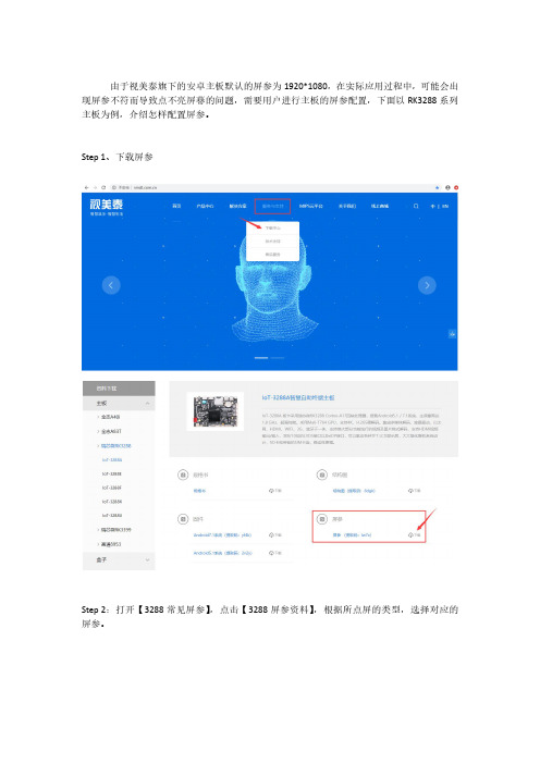
由于视美泰旗下的安卓主板默认的屏参为1920*1080,在实际应用过程中,可能会出现屏参不符而导致点不亮屏幕的问题,需要用户进行主板的屏参配置,下面以RK3288系列主板为例,介绍怎样配置屏参。
Step1、下载屏参
Step2:打开【3288常见屏参】,点击【3288屏参资料】,根据所点屏的类型,选择对应的屏参。
以点LVDS屏为例,打开【LVDS】文件夹,根据所点屏的分辨率打开对应的屏参,找到display_param.cfg
Step3、将文件放到U盘的根目录.
注:全志CPU系列安卓主板使用sd卡或者TF卡
瑞芯微CPU系列安卓主板使用U盘2.0
Step4:将存储卡插入安卓主板,然后给主板上电。
系统会自动读取屏参,开机时跟平时一样(主板刷屏参时系统指示灯会闪烁三下红灯)。
Step5:1种分辨率,只要配置一次屏参,主板即可自行永久保存,配置后成功后即可拔除存储卡。
RK3288硬件参数解读
RK3288硬件参数解读性能提升50%!最新ARM神秘内核RK3288硬件参数解读在拉斯维加斯CES 2014 上,瑞芯微带来全新的RK3288处理器:“全球第一个四核ARM 全新内核芯片、全球第一个支持最新超强Mali-T76x系列GPU的芯片以及全球第一个4Kx2K 硬解H.265的芯片”而被业界关注。
平板知名OEM厂商包括原道、五元素、驰为等纷纷跟随新品蓄势待发。
本文将从硬件参数对RK3288进行解读,看看参数背后代表了什么意义。
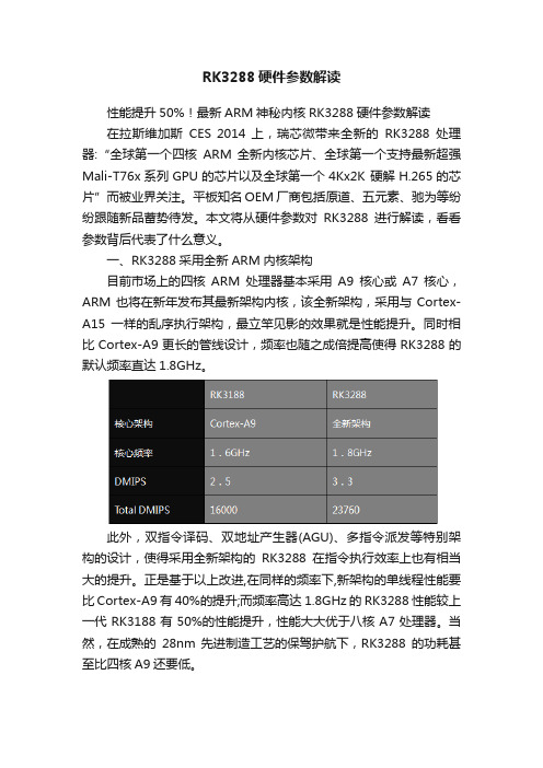
一、RK3288采用全新ARM内核架构目前市场上的四核ARM处理器基本采用A9核心或A7核心,ARM也将在新年发布其最新架构内核,该全新架构,采用与Cortex-A15一样的乱序执行架构,最立竿见影的效果就是性能提升。
同时相比Cortex-A9更长的管线设计,频率也随之成倍提高使得RK3288的默认频率直达1.8GHz。
此外,双指令译码、双地址产生器(AGU)、多指令派发等特别架构的设计,使得采用全新架构的RK3288在指令执行效率上也有相当大的提升。
正是基于以上改进,在同样的频率下,新架构的单线程性能要比Cortex-A9有40%的提升;而频率高达1.8GHz的RK3288性能较上一代RK3188有50%的性能提升,性能大大优于八核A7处理器。
当然,在成熟的28nm 先进制造工艺的保驾护航下,RK3288的功耗甚至比四核A9还要低。
二、RK3288采用最强移动GPU,性能媲美桌面GPURK3288所采用的GPU让人非常震撼——最新、最强的Mali T76X核心! Mali T76X 是ARM最新Mali T700系列GPU最强的型号,拥有16个着色器核心,性能直逼桌面显卡。
以RK3288所采用的Mali T764核心为例,性能高达性能高达82 GFLOPS、2400M pixel/s,性能比Mali-T604GPU提升400%,而比目前市场主流的Mali-400MP4整整提升了500%,绝对是最快的移动GPU。
- 1、下载文档前请自行甄别文档内容的完整性,平台不提供额外的编辑、内容补充、找答案等附加服务。
- 2、"仅部分预览"的文档,不可在线预览部分如存在完整性等问题,可反馈申请退款(可完整预览的文档不适用该条件!)。
- 3、如文档侵犯您的权益,请联系客服反馈,我们会尽快为您处理(人工客服工作时间:9:00-18:30)。
3288四核安卓高清驱动板
规格书
产品型号:3288
版本:V1.0
编制:
审核:
复审:
批准:发布日期:
2017-05-05
DUI2017
在开始使板卡前,请仔细通读本规格书,并严格按照规格书上的描述进行操作
目录:
1. 产品概述 -------------------------------------------------------------------------------------------------- 3
2. 产品特性说明---------------------------------------------------------------------------------------------3
3. 产品外观 --------------------------------------------------------------------------------------------------- 4
4. 按键板 ------------------------------------------------------------------------------------------------------ 6
5. 接口定义 --------------------------------------------------------------------------------------------------- 7
6. 产品结构图 ------------------------------------------------------------------------------------------------ 12
7. 使用注意事项--------------------------------------------------------------------------------------------- 12
声明:
●本规格书的说明文字及图解有可能与实物有差别,请以实物为准。
●奉行持续研发的政策,我司保留对本文所描述之任何产品进行更改及改进的权利,恕不另行通知。
1. 产品概述:
3288 采用 RK3288 主芯片,RK3288 是一颗 Cortex-A17 架构的四核处理器,最高频率才可以达到 1.8GHZ,性能较 RK3188 的 Cortex-A9 架构提升了 60%, GPU 采用的是 Mali-T760,性能较 Mali-T400 提升了 500%;搭载 Android 5.1 系统,标配 2GB DDR3 和 8GB INAND;支持双10 位的 LVDS 输出(最高支持 1920*1080),支持 EDP 输出(最高支持 2560*1600),支持单路 MIPI 输出(最高支持 1920*1080);支持 HDMI 输出(最高支持 4K);支持 6 个 USB 接口和 4 个 UART(TTL/232 可选)扩展口;支持 5 路 GPIO 和 1 路 ADC;支持 1 路 I2C 触摸接口;支持 1 路 MINI-PCIE 3G/4G 接口;支持 100M 网口,WIFI,蓝牙;支持远程定时开关机,软件看门口,系统自恢复,真正实现智能化管理。
Series is a是一款适用于 435 是一款适用于 4K2K 60HZ 超高清屏的液晶显示驱动板。
它支持 4K@HZ 信号输入,支持 10bit 8-lane VB1 或 8-lane EDP 接口的屏,最大分辨率可达 4096X2160@60HZ。
2. 产品特性说明:
3. 产品外观:
正面:
背面:
4. 按键和指示灯:
5. 接口定义:
◆ JP12 电源输入扩展口
◆ JP11 UART3 串口(TTL/232 可选,默认232)
◆J17 GPIO 输入/输出,ADC
◆JP5 EDP 背光控制
◆ J704 LVDS 屏显示电压选择接口
◆ J705 EDP 屏显示电压选择接口
◆ J5200 MIPI 屏显示接口(需定制排线可接MIPI 屏)◆ K3 系统烧录升级按键
6. 产品结构图:
PCB 长:146mm ,PCB 宽:104mm,螺丝孔3mm,板总体高度约13mm
7. 使用注意事项
⏹相对湿度: 80%
⏹存储温度:0°C – 60°C
⏹使用温度:0°C – 40°C
⏹请使板卡远离静电
⏹请确保板卡工作时远离导体
⏹板卡工作时请勿拆解
⏹勿受重压及弯曲变形
⏹如果板卡上有灰尘,请用干布擦拭
⏹正确接好屏线前请勿接通电源。