A4931 datasheet 中文+总结
4CMC331M450AK8中文资料

2,000 h at 85 °C and full load∆ Capacitance ±20% ESR 200% of limit DCL 100% of limit3,000 h at 85 ºC with rated voltage∆ Capacitance ±10% ESR 200% of limit DCL 100% of limit500 h at 85 °C, capacitance, ESR and DCL, initial requirements10 to 55 Hz, 0.06” and 10 g max, 2 h each planeThe Type 4CMC is the PC-mount version of the high-capacitance Type DCMC screw-terminal capacitor and has about 50% more capacitance per can size through 250 V. It’s for bus filtering applications where more capacitance or smaller can size is important like welders and energy storage. It’s a much better value than a large snap-in capacitor. Its extended cathode foil assures cool operation with heatflow from the capacitor element to the can in all mounting orientations.Highlights• Much better value than large snap-in capacitor • Ripple Currents to > 50 amps at 55 °C • 3-leads for reverse proof, strong mounting • Printed-circuit mounting version of DCMC • Thermal-Pak™ extended cathode constructionSpecificationsOperating Temperature:Rated Voltage:Capacitance:Capacitance Tolerance:DC Leakage Current:Cold Impedance:Ripple Current Multipliers:EIA Ripple Life: Life Test:Shelf Life Test: Vibration: Best Value Printed Circuit Mount TypeFrequency–40 °C to +85 °C 16 to 500 Vdc210 µF to 420,000 µF ± 20%± 20%≤ 6 √CV µA, 6 max, 5 min.–20 °C multiple of 25 °C Z ≤ 8 for 16 to 50 V, 4 for 63 to 100 V, 3 for 160 V & up Ambient Temperature45 °C 55 °C 65 °C 75 °C 85 °C 2.002.001.731.411.0050 Hz 60 Hz 120 Hz 360 Hz 1 kHz 5 kHk-10 kHz & up6.3 to 50 V 0.800.85 1.00 1.05 1.08 1.08 1.0863 to 250 V 0.800.83 1.00 1.15 1.20 1.20 1.20300 to 5000.780.801.001.301.401.401.40Complies with the EU Directive 2002/95/EC requirement restricting the use of Lead (Pb), Mercury (Hg), Cadmium (Cd), Hexavalent chromium (Cr(VI)), PolyBrominated Biphenyls (PBB) and PolyBrominated Diphenyl Ethers (PBDE).Outline DrawingsCase DimensionsPart Numbering System4CMCType 8InsulationAKCase Code100Voltage M Tolerance382Capacitance(blank) = StraightLeads0 = Bare can 8 = PVC and Standoffs9 = Polyester and Standoffs6R3 = 6.3 V 063 = 63 V M = ±20%T = –10% +50% U = –10 +75% 382 = 3800 µF 212 = 2100 µF100 = 100 VCase InchesMillimeters Code D ± .031 L MAX C ± .015 S ± .031 E ± .031 F ± .015 D ± .78 L MAX C ± .78 S ± .78 E ± .78 F ± .38AK 1.375 1.750.500.1750.250.5534.9344.4512.70 4.45 6.3513.97 AA 1.375 2.250.500.1750.250.5534.9357.1512.70 4.45 6.3513.97 AH 1.375 2.750.500.1750.250.5534.9869.8512.70 4.45 6.3513.97 AB 1.375 3.250.500.1750.250.5534.9382.5512.70 4.45 6.3513.97 AJ 1.375 3.750.500.1750.250.5534.9395.2512.70 4.45 6.3513.97 AC 1.375 4.250.500.1750.250.5534.93107.9512.70 4.45 6.3513.97 AD 1.375 4.750.500.1750.250.5534.93120.6512.70 4.45 6.3513.97 AE 1.375 5.250.500.1750.250.5534.93133.3512.70 4.45 6.3513.97 AF 1.375 5.750.500.1750.250.5534.93146.0512.70 4.45 6.3513.97 EA 1.75 2.250.700.3750.350.9044.4557.1517.789.538.8922.86 EH 1.75 2.750.700.3750.350.9044.4569.8517.789.538.8922.86 EB 1.75 3.250.700.3750.350.9044.4582.5517.789.538.8922.86 EJ 1.75 3.750.700.3750.350.9044.4595.2517.789.538.8922.86 EC 1.75 4.250.700.3750.350.9044.45107.9517.789.538.8922.86 ED 1.75 4.750.700.3750.350.9044.45120.6517.789.538.8922.86 EE 1.75 5.250.700.3750.350.9044.45133.3517.789.538.8922.86 EF 1.75 5.750.700.3750.350.9044.45146.0517.789.538.8922.86 BA 2.00 2.250.800.4250.40 1.0050.8057.1520.3210.8010.1625.40 BH 2.00 2.750.800.4250.40 1.0050.8069.8520.3210.8010.1625.40 BB 2.00 3.250.800.4250.40 1.0050.8082.5520.3210.8010.1625.40 BJ 2.00 3.750.800.4250.40 1.0050.8095.2520.3210.8010.1625.40 BC 2.00 4.250.800.4250.40 1.0050.80107.9520.3210.8010.1625.40 BD 2.00 4.750.800.4250.40 1.0050.80120.6520.3210.8010.1625.40 BE 2.00 5.250.800.4250.40 1.0050.80133.2520.3210.8010.1625.40 BF2.005.750.800.4250.401.0050.80146.0520.3210.8010.1625.40RatingsESR Max. 25 ºC 120 Hz 20 kHz (mΩ) (mΩ)Ripple Amps,85 ºC 120 Hz 20 kHz (A) (A)Nominal Size D X L (in)ESR Max. 25 ºC 120 Hz 20 kHz (mΩ) (mΩ)Ripple Amps,85 ºC 120 Hz 20 kHz (A) (A)Nominal Size D X L (in)Cap.(µF)Catalog Part NumberCap.(µF)Catalog Part Number 16 Vdc (20 Vdc Surge)2000004CMC204M016AF8 10.38.216.919.0 1 3/8 X 5 3/4 330004CMC333M016AK8 34.227.2 5.7 6.4 1 3/8 X 1 3/4 2200004CMC224M016EC8 1310.315.217 1 3/4 X 4 1/4 550004CMC553M016AA821.216.98.49.4 1 3/8 X 2 1/4 2400004CMC244M016BJ8 11.79.315.617.5 2 X 3 3/4 770004CMC773M016AH8 18.314.69.310.4 1 3/8 X 2 3/4 2500004CMC254M016ED8 11.59.21719 1 3/4 X 4 3/4 790004CMC793M016EA8 23.018.39.210.4 1 3/4 X 2 1/4 2800004CMC284M016EE8 10.58.418.921.2 1 3/4 X 5 1/4 990004CMC993M016AB814.811.811.112.4 1 3/8 X 3 1/4 2800004CMC284M016BC8 11.49.115.917.8 2 X 4 1/4 1100004CMC114M016EH8 17.413.811.412.7 1 3/4 X 2 3/4 3100004CMC314M016EF8 9.77.721.023.5 1 3/4 X 5 3/4 1200004CMC124M016AJ8 12.810.212.514.0 1 3/8 X 3 3/4 3300004CMC334M016BD8 10.78.516.919 2 X 4 3/4 1200004CMC124M016BA817.714.110.011.2 2 X 2 1/4 3700004CMC374M016BE8 10.08.018.120.3 2 X 5 1/4 1400004CMC144M016AC8 12.59.913.315.0 1 3/8 X 4 1/4 4200004CMC424M016BF89.07.219.822.22 X 5 3/41400004CMC144M016EB815.812.612.914.4 1 3/4 X 3 1/4 25 Vdc (30 Vdc Surge) 1500004CMC154M016BH8 14.511.611.913.3 2 X 2 3/4 220004CMC223M025AK8 63.250.4 4.2 4.7 1 3/8 X 1 3/4 1600004CMC164M016AD8 11.59.114.516.2 1 3/8 X 4 3/4 370004CMC373M025AA8 23.919.17.98.8 1 3/8 X 2 1/4 1800004CMC184M016AE8 10.88.615.817.7 1 3/8 X 5 1/4 520004CMC523M025AH8 20.616.48.89.8 1 3/8 X 2 3/4 1800004CMC184M016EJ8 15.012.013.615.3 1 3/4 X 3 3/4 540004CMC543M025EA8 22.918.39.310.4 1 3/4 X 2 1/4 1900004CMC194M016BB812.39.813.615.22 X3 1/4670004CMC673M025AB816.613.210.511.71 3/8 X 3 1/4Typical Performance CurvesESR Max.25 ºC 120 Hz 20 kHz (mΩ) (mΩ)Ripple Amps,85 ºC120 Hz 20 kHz(A) (A)NominalSizeD X L(in)ESR Max.25 ºC120 Hz 20 kHz(mΩ) (mΩ)Ripple Amps,85 ºC120 Hz 20 kHz(A) (A)NominalSizeD X L(in)Cap. (µF)Catalog PartNumberCap.(µF)Catalog PartNumber780004CMC783M025EH8 19.0015.1010.9012.20 1 3/4 X 2 3/4 50 Vdc (65 Vdc Surge)820004CMC823M025AJ8 14.3011.4011.8013.20 1 3/8 X 3 3/4 100004CMC103M050AK8 44.3035.30 5.00 5.70 1 3/8 X 1 3/4 830004CMC833M025BA8 19.0015.2010.9012.20 2 X 2 1/4 170004CMC173M050AA8 27.3021.807.408.20 1 3/8 X 2 1/4 970004CMC973M025AC8 13.9011.1012.6014.20 1 3/8 X 4 1/4 240004CMC243M050AH8 23.4018.708.209.20 1 3/8 X 2 3/4 1000004CMC104M025BH8 15.5012.4013.0014.60 2 X 2 3/4 270004CMC273M050EA8 28.2022.508.409.40 1 3/4 X 2 1/4 1000004CMC1003M025EB8 17.3013.8012.3013.80 1 3/4 X 3 1/4 310004CMC313M050AB8 18.9015.109.8011.00 1 3/8 X 3 1/4 1100004CMC114M025AD8 12.8010.2013.8015.40 1 3/8 X 4 3/4 330004CMC333M050BA8 27.9022.309.0010.10 2 X 2 1/4 1200004CMC124M025AE8 11.909.5015.0016.80 1 3/8 X 5 1/4 360004CMC363M050EH8 21.2016.9010.3011.50 1 3/4 X 2 3/4 1200004CMC124M025EJ8 16.4013.0013.1014.60 1 3/4 X 3 3/4 380004CMC383M050AJ8 16.2013.0011.1012.40 1 3/8 X 3 3/4 1300004CMC134M025BB8 12.7010.1015.2017.00 2 X 3 1/4 390004CMC393M050EB8 20.3016.2011.3012.70 1 3/4 X 3 1/4 1400004CMC144M025AF8 11.409.1016.1018.00 1 3/8 X 5 3/4 450004CMC453M050AC8 15.7012.5011.9013.30 1 3/8 X 4 1/4 1500004CMC154M025EC8 14.1011.2014.6016.30 1 3/4 X 4 1/4 470004CMC473M050AD8 14.9011.9012.7014.30 1 3/8 X 4 3/4 1600004CMC164M025BJ8 12.5010.0017.1019.20 2 X 3 3/4 470004CMC473M050BH8 19.6015.6011.6013.00 2 X 2 3/4 1700004CMC174M025ED8 12.5010.0016.3018.30 1 3/4 X 4 3/4 480004CMC483M050EJ8 19.2015.3012.1013.50 1 3/4 X 3 3/4 1900004CMC194M025EE8 11.309.0018.2020.40 1 3/4 X 5 1/4 530004CMC533M050AE8 13.9011.0013.9015.60 1 3/8 X 5 1/4 1900004CMC194M025BC8 12.209.7017.4019.50 2 X 4 1/4 560004CMC563M050BB8 16.3013.0013.4015.00 2 X 3 1/4 2100004CMC214M025EF8 10.508.3020.2022.60 1 3/4 X 5 3/4580004CMC583M050EC8 16.5013.1013.5015.10 1 3/4 X 4 1/4 2200004CMC224M025BD8 11.409.1018.6020.80 2 X 4 3/4600004CMC603M050AF8 13.2010.5015.0016.80 1 3/8 X 5 3/4 2500004CMC254M025BE8 10.608.5019.9022.30 2 X 5 1/4670004CMC673M050ED8 14.5011.6015.1017.00 1 3/4 X 4 3/4 2800004CMC284M025BF8 9.607.6021.8024.40 2 X 5 3/4680004CMC683M050BJ8 15.0012.0015.6017.50 2 X 3 3/435 Vdc (40 Vdc Surge) 760004CMC763M050EE8 13.1010.5016.9018.90 1 3/4 X 5 1/4 150004CMC153M035AK8 63.2050.40 4.20 4.70 1 3/8 X 1 3/4820004CMC823M050BC8 14.3011.4016.1018.00 2 X 4 1/4 250004CMC253M035AA8 23.9019.107.908.80 1 3/8 X 2 1/4850004CMC853M050EF8 12.109.6018.8021.10 1 3/4 X 5 3/4 350004CMC353M035AH8 20.6016.408.809.80 1 3/8 X 2 3/4910004CMC913M050BD8 12.7010.1017.6019.80 2 X 4 3/4 380004CMC383M035EA8 22.7018.109.3010.40 1 3/4 X 2 1/41000004CMC104M050BE8 11.809.4019.0021.30 2 X 5 1/4 450004CMC453M035AB8 16.6013.2010.5011.70 1 3/8 X 3 1/41200004CMC124M050BF8 10.508.4020.7023.20 2 X 5 3/4 520004CMC523M035EH8 19.0015.1010.9012.20 1 3/4 X 2 3/463 Vdc (75 Vdc Surge)550004CMC553M035AJ8 14.3011.4011.8013.20 1 3/8 X 3 3/475004CMC752M063AK8 44.1035.10 5.10 5.70 1 3/8 X 1 3/4 560004CMC563M035BA8 19.0015.2010.9012.20 2 X 2 1/4120004CMC123M063AA8 26.8021.407.408.30 1 3/8 X 2 1/4 650004CMC653M035AC8 13.9011.1012.6014.20 1 3/8 X 4 1/4160004CMC163M063EA8 28.2022.508.309.30 1 3/4 X 2 1/4 670004CMC673M035EB8 17.3013.8012.3013.80 1 3/4 X 3 1/4160004CMC163M063AH8 23.5018.808.209.20 1 3/8 X 2 3/4 680004CMC683M035BH8 15.5012.4013.0014.60 2 X 2 3/4210004CMC213M063AB8 18.7014.909.9011.10 1 3/8 X 3 1/4 750004CMC753M035AD8 12.8010.2013.8015.40 1 3/8 X 4 3/4220004CMC223M063EH8 21.2016.9010.3011.50 1 3/4 X 2 3/4 830004CMC833M035EJ8 16.4013.0013.1014.60 1 3/4 X 3 3/4260004CMC263M063AJ8 16.9013.5010.9012.20 1 3/8 X 3 3/4 840004CMC843M035AE8 11.909.5015.2017.10 1 3/8 X 5 1/4260004CMC263M063BA8 27.7022.109.0010.10 2 X 2 1/4 870004CMC873M035BB8 12.7010.1015.2017.00 2 X 3 1/4290004CMC293M063EB8 20.9016.7011.2012.50 1 3/4 X 3 1/4 930004CMC933M035AF8 11.409.1016.1018.10 1 3/8 X 5 3/4300004CMC303M063AC8 17.3013.8011.3012.70 1 3/8 X 4 1/4 1000004CMC104M035EC8 14.1011.2014.6016.30 1 3/4 X 4 1/4330004CMC333M063BH8 19.5015.5011.6013.00 2 X 2 3/4 1100004CMC114M035BJ8 12.5010.0017.1019.20 2 X 3 3/4350004CMC353M063AD8 15.7012.5012.4013.90 1 3/8 X 4 3/4 1100004CMC114M035ED8 12.5010.0016.3018.30 1 3/4 X 4 3/4360004CMC363M063EJ8 20.0016.0011.8013.20 1 3/4 X 3 3/4 1300004CMC134M035EE8 11.309.0018.2020.40 1 3/4 X 5 1/4380004CMC383M063AE8 14.5011.5013.8015.50 1 3/8 X 5 1/4 1300004CMC134M035BC8 12.209.7017.4019.50 2 X 4 1/4430004CMC433M063EC8 17.2013.7013.2014.80 1 3/4 X 4 1/4 1400004CMC144M035EF8 10.508.3020.2022.60 1 3/4 X 5 3/4440004CMC443M063AF8 13.7010.9014.7016.50 1 3/8 X 5 3/4 1500004CMC154M035BD8 11.409.1018.6020.80 2 X 4 3/4470004CMC473M063BB8 16.2012.9013.4015.00 2 X 3 1/4 1700004CMC174M035BE8 10.608.5020.0022.40 2 X 5 1/4500004CMC503M063ED8 15.2012.2014.8016.60 1 3/4 X 4 3/4 1900004CMC194M035BF8 9.607.6021.7024.40 2 X 5 3/4530004CMC533M063BJ8 15.1012.0015.6017.40 2 X 3 3/4570004CMC573M063EE8 13.8011.0016.5018.50 1 3/4 X 5 1/4ESR Max.25 ºC 120 Hz 20 kHz (mΩ) (mΩ)Ripple Amps,85 ºC120 Hz 20 kHz(A) (A)NominalSizeD X L(in)ESR Max.25 ºC120 Hz 20 kHz(mΩ) (mΩ)Ripple Amps,85 ºC120 Hz 20 kHz(A) (A)NominalSizeD X L(in)Cap. (µF)Catalog PartNumberCap.(µF)Catalog PartNumber590004CMC593M063BC8 14.5011.5016.0017.90 2 X 4 1/4220004CMC223M100AF8 20.1016.0012.1013.60 1 3/8 X 5 3/4 640004CMC643M063EF8 12.7010.1018.4020.60 1 3/4 X 5 3/4220004CMC223M100EC8 21.9017.5011.7013.10 1 3/4 X 4 1/4 690004CMC693M063BD8 12.8010.2017.6019.70 2 X 4 3/4260004CMC263M100ED8 19.3015.4013.2014.70 1 3/4 X 4 3/4 790004CMC793M063BE8 11.609.2019.1021.40 2 X 5 1/4260004CMC263M100BJ8 23.6018.8012.5013.90 2 X 3 3/4 890004CMC893M063BF8 10.708.5020.6023.10 2 X 5 3/4300004CMC303M100EE8 17.3013.8014.7016.50 1 3/4 X 5 1/480 Vdc (100 Vdc Surge) 300004CMC303M100BC8 20.2016.1013.5015.20 2 X 4 1/4 56004CMC562M080AK8 59.6047.50 4.40 4.90 1 3/8 X 1 3/4330004CMC333M100EF8 15.8012.6016.4018.40 1 3/4 X 5 3/4 85004CMC852M080AA8 36.2028.80 6.407.20 1 3/8 X 2 1/4350004CMC353M100BD8 17.8014.2014.9016.70 2 X 4 3/4 120004CMC123M080EA8 38.4030.607.208.00 1 3/4 X 2 1/4400004CMC403M100BE8 16.1012.8016.3018.20 2 X 5 1/4 120004CMC123M080AH8 31.5025.107.107.90 1 3/8 X 2 3/4450004CMC453M100BF8 14.7011.7017.5019.60 2 X 5 3/4 150004CMC153M080AB8 31.6025.207.608.50 1 3/8 X 3 1/4160 Vdc (200 Vdc Surge)170004CMC173M080EH8 34.0027.108.109.10 1 3/4 X 2 3/415004CMC152M160AK8 81.7065.20 3.70 4.20 1 3/8 X 1 3/4 180004CMC183M080BA8 32.8026.108.309.30 2 X 2 1/425004CMC252M160AA8 51.8041.30 5.30 6.00 1 3/8 X 2 1/4 190004CMC193M080AJ8 25.2020.108.9010.00 1 3/8 X 3 3/435004CMC352M160AH8 37.5029.90 6.507.30 1 3/8 X 2 3/4 220004CMC223M080AC8 20.9016.7010.3011.50 1 3/8 X 4 1/437004CMC372M160EA8 47.1037.50 6.10 6.90 1 3/4 X 2 1/4 220004CMC223M080EB8 30.5024.309.3010.40 1 3/4 X 3 1/445004CMC452M160AB8 29.6023.607.808.80 1 3/8 X 3 1/4 230004CMC233M080BH8 23.1018.4010.7011.90 2 X 2 3/448004CMC482M160BA8 35.4028.207.208.10 2 X 2 1/4 260004CMC263M080AD8 19.1015.2011.2012.60 1 3/8 X 4 3/452004CMC522M160EH8 29.0023.108.309.30 1 3/4 X 2 3/4 270004CMC273M080EJ8 25.1020.0010.5011.80 1 3/4 X 3 3/455004CMC552M160AJ8 23.5018.7029.3032.80 1 3/8 X 3 3/4 290004CMC293M080AE8 17.7014.1012.5014.00 1 3/8 X 5 1/466004CMC662M160AC8 20.2016.1010.5011.70 1 3/8 X 4 1/4 300004CMC303M080BB8 19.2015.3012.3013.80 2 X 3 1/468004CMC682M160EB8 22.5017.9010.2011.50 1 3/4 X 3 1/4 320004CMC323M080AF8 16.7013.3013.3014.90 1 3/8 X 5 3/471004CMC712M160AD8 18.6014.8011.4012.80 1 3/8 X 4 3/4 320004CMC323M080EC8 21.5017.1011.8013.20 1 3/4 X 4 1/471004CMC712M160BH8 26.5021.209.0010.10 2 X 2 3/4 370004CMC373M080BJ8 18.0014.3014.3016.00 2 X 3 3/480004CMC802M160AE8 16.8013.4012.6014.20 1 3/8 X 5 1/4 370004CMC373M080ED8 18.9015.1013.3014.90 1 3/4 X 4 3/483004CMC832M160EJ8 18.5014.7011.7013.10 1 3/4 X 3 3/4 430004CMC433M080BC8 15.9012.6015.3017.10 2 X 4 1/490004CMC902M160AF8 19.2015.3012.4013.90 1 3/8 X 5 3/4 430004CMC433M080EE8 17.0013.6014.8016.60 1 3/4 X 5 1/493004CMC932M160BB8 20.6016.4010.8012.10 2 X 3 1/4 480004CMC483M080EF8 15.6012.4016.6018.60 1 3/4 X 5 3/4100004CMC1002M160EC8 15.8012.6013.1014.60 1 3/4 X 4 1/4 500004CMC503M080BD8 13.6010.8017.1019.10 2 X 4 3/4110004CMC113M160BJ8 16.9013.5013.3014.90 2 X 3 3/4 580004CMC583M080BE8 12.209.7018.6020.90 2 X 5 1/4120004CMC123M160ED8 13.9011.1014.7016.50 1 3/4 X 4 3/4 650004CMC653M080BF8 11.208.9020.1022.50 2 X 5 3/4130004CMC133M160EE8 12.509.9016.5018.40 1 3/4 X 5 1/4 100 Vdc (125 Vdc Surge) 130004CMC133M160BC8 14.5011.6014.5016.20 2 X 4 1/4 38004CMC382M100AK8 58.6046.70 4.40 4.90 1 3/8 X 1 3/4150004CMC153M160EF8 11.409.1018.4020.60 1 3/4 X 5 3/4 63004CMC632M100AA8 35.6028.30 6.507.20 1 3/8 X 2 1/4160004CMC163M160BD8 12.8010.2015.9017.80 2 X 4 3/4 81004CMC812M100AH8 32.8026.20 2.20 2.50 1 3/8 X 2 3/4180004CMC183M160BE8 11.509.2017.4019.50 2 X 5 1/4 82004CMC822M100EA8 39.2031.207.107.90 1 3/4 X 2 1/4200004CMC203M160BF8 10.508.4018.8021.00 2 X 5 3/4 100004CMC103M100AB8 32.9026.207.408.30 1 3/8 X 3 1/4200 Vdc (250 Vdc Surge)110004CMC113M100BA8 35.9028.707.908.90 2 X 2 1/412004CMC122M200AK8 105.2060.40 3.10 4.10 1 3/8 X 1 3/4 120004CMC123M100EH8 34.7027.708.009.00 1 3/4 X 2 3/419004CMC192M200AA8 66.6038.20 4.50 5.90 1 3/8 X 2 1/4 130004CMC133M100AJ8 31.7025.307.908.90 1 3/8 X 3 3/427004CMC272M200AH8 48.0027.60 5.407.20 1 3/8 X 2 3/4 150004CMC153M100EB8 31.1024.809.2010.30 1 3/4 X 3 1/427004CMC272M200EA8 60.0034.40 5.307.00 1 3/4 X 2 1/4 150004CMC153M100AC8 27.4021.800.90 1.10 1 3/8 X 4 1/435004CMC352M200AB8 37.8021.70 6.608.70 1 3/8 X 3 1/4 160004CMC163M100BH8 26.4021.0010.0011.20 2 X 2 3/435004CMC352M200BA8 44.2030.70 6.607.90 2 X 2 1/4 170004CMC173M100AD8 24.2019.3010.0011.20 1 3/8 X 4 3/437004CMC372M200EH8 38.1021.90 6.909.10 1 3/4 X 2 3/4 190004CMC193M100EJ8 25.6020.4010.4011.70 1 3/4 X 3 3/443004CMC432M200AJ8 29.9017.207.8010.20 1 3/8 X 3 3/4 200004CMC203M100AE8 21.9017.5011.2012.60 1 3/8 X 5 1/448004CMC482M200EB8 29.4016.908.5011.20 1 3/4 X 3 1/4 210004CMC213M100BB8 22.9018.3011.3012.60 2 X 3 1/450004CMC502M200BH8 33.1023.008.209.80 2 X 2 3/4ESR Max.25 ºC 120 Hz 20 kHz (mΩ) (mΩ)Ripple Amps,85 ºC120 Hz 20 kHz(A) (A)NominalSizeD X L(in)ESR Max.25 ºC120 Hz 20 kHz(mΩ) (mΩ)Ripple Amps,85 ºC120 Hz 20 kHz(A) (A)NominalSizeD X L(in)Cap. (µF)Catalog PartNumberCap.(µF)Catalog PartNumber51004CMC512M200AC8 25.7014.708.8011.70 1 3/8 X 4 1/416004CMC162M300AB8 82.7047.50 4.80 6.30 1 3/8 X 3 1/4 58004CMC582M200AD8 22.6013.009.8012.90 1 3/8 X 4 3/418004CMC182M300EH8 99.2056.90 4.80 6.30 1 3/4 X 2 3/4 59004CMC592M200EJ8 24.1013.809.7012.70 1 3/4 X 3 3/419004CMC192M300AJ8 68.0039.00 5.607.40 1 3/8 X 3 3/4 66004CMC662M200AE8 20.3011.6010.9014.40 1 3/8 X 5 1/422004CMC222M300BH8 67.1037.40 6.308.40 2 X 2 3/4 68004CMC682M200BB8 25.6017.809.8011.80 2 X 3 1/423004CMC232M300AC8 57.9033.20 6.408.40 1 3/8 X 4 1/4 71004CMC712M200EC8 20.5011.8010.8014.30 1 3/4 X 4 1/423004CMC232M300EB8 76.1043.70 5.807.70 1 3/4 X 3 1/4 74004CMC742M200AF8 23.1013.3010.7014.20 1 3/8 X 5 3/426004CMC262M300AD8 50.6029.007.109.40 1 3/8 X 4 3/4 81004CMC812M200BJ8 21.0014.6012.2014.60 2 X 3 3/429004CMC292M300AE8 45.0025.807.8010.30 1 3/8 X 5 1/4 82004CMC822M200ED8 17.9010.3012.2016.10 1 3/4 X 4 3/429004CMC292M300BB8 51.6028.707.6010.20 2 X 3 1/4 93004CMC932M200EE8 16.009.2013.7018.10 1 3/4 X 5 1/429004CMC292M300EJ8 61.9035.50 6.808.90 1 3/4 X 3 3/4 95004CMC952M200BC8 19.1013.3012.8015.40 2 X 4 1/433004CMC332M300AF8 50.7029.107.6010.10 1 3/8 X 5 3/4 100004CMC103M200EF8 14.508.3015.4020.30 1 3/4 X 5 3/435004CMC352M300EC8 52.2030.007.7010.20 1 3/4 X 4 1/4 110004CMC113M200BD8 15.7010.9014.6017.50 2 X 4 3/436004CMC362M300BJ8 51.2028.508.1010.80 2 X 3 3/4 120004CMC123M200BE8 14.109.8016.0019.20 2 X 5 1/440004CMC402M300ED8 45.3026.008.6011.40 1 3/4 X 4 3/4 140004CMC143M200BF8 12.808.9017.3020.80 2 X 5 3/443004CMC432M300BC8 43.3024.109.2012.30 2 X 4 1/4 250 Vdc (300 Vdc Surge)46004CMC462M300EE8 40.1023.009.5012.60 1 3/4 X 5 1/4 8904CMC891M250AK8 137.0078.60 2.60 3.40 1 3/8 X 1 3/449004CMC492M300BD8 38.0021.2010.2013.70 2 X 4 3/4 15004CMC152M250AA8 86.5049.70 3.70 4.90 1 3/8 X 2 1/451004CMC512M300EF8 36.0020.6010.4013.70 1 3/4 X 5 3/4 19004CMC192M250EA8 68.7039.40 4.80 6.30 1 3/4 X 2 1/457004CMC572M300BE8 33.3018.5011.3015.10 2 X 5 1/4 21004CMC212M250AH8 62.3035.70 4.50 6.00 1 3/8 X 2 3/464004CMC642M300BF8 29.9016.7012.3016.50 2 X 5 3/4 27004CMC272M250BA8 54.2037.60 5.807.00 2 X 2 1/4350 Vdc (400 Vdc Surge)27004CMC272M250AB8 48.8028.00 5.507.20 1 3/8 X 3 1/44304CMC431M350AK8 264.10151.60 2.10 2.80 1 3/8 X 1 3/4 28004CMC282M250EH8 47.8027.40 6.108.10 1 3/4 X 2 3/47104CMC711M350AA8 158.9091.20 3.10 4.00 1 3/8 X 2 1/4 32004CMC322M250AJ8 38.6022.10 6.508.50 1 3/8 X 3 3/410004CMC102M350EA8 119.2068.40 4.10 5.40 1 3/4 X 2 1/4 37004CMC372M250EB8 36.8021.107.6010.00 1 3/4 X 3 1/410004CMC102M350AH8 113.9065.40 3.70 4.90 1 3/8 X 2 3/4 38004CMC382M250BH8 40.5028.107.208.70 2 X 2 3/412004CMC122M350BA8 98.1054.60 4.80 6.40 2 X 2 1/4 39004CMC392M250AC8 33.0018.907.409.70 1 3/8 X 4 1/413004CMC132M350EH8 105.1060.30 4.60 6.10 1 3/4 X 2 3/4 44004CMC442M250AD8 29.0016.608.2010.80 1 3/8 X 4 3/413004CMC132M350AB8 89.0051.10 4.50 6.00 1 3/8 X 3 1/4 45004CMC452M250EJ8 30.1017.308.6011.40 1 3/4 X 3 3/416004CMC162M350BH8 71.8040.00 6.008.10 2 X 2 3/4 50004CMC502M250AE8 25.9014.909.1012.00 1 3/8 X 5 1/416004CMC162M350AJ8 73.2042.00 5.20 6.90 1 3/8 X 3 3/4 50004CMC502M250BB8 31.2021.708.7010.40 2 X 3 1/417004CMC172M350EB8 80.6046.30 5.707.50 1 3/4 X 3 1/4 54004CMC542M250EC8 25.5014.709.7012.80 1 3/4 X 4 1/418004CMC182M350AC8 62.3035.80 6.007.90 1 3/8 X 4 1/4 56004CMC562M250AF8 29.4016.909.0011.90 1 3/8 X 5 3/421004CMC212M350BB8 55.1030.707.309.70 2 X 3 1/4 62004CMC622M250BJ8 25.5017.7010.7012.90 2 X 3 3/421004CMC212M350AD8 54.4031.20 6.708.80 1 3/8 X 4 3/4 63004CMC632M250ED8 22.3012.8011.0014.50 1 3/4 X 4 3/421004CMC212M350EJ8 65.5037.60 6.508.60 1 3/4 X 3 3/4 72004CMC722M250EE8 19.8011.4012.3016.30 1 3/4 X 5 1/424004CMC242M350AE8 48.3027.707.409.80 1 3/8 X 5 1/4 73004CMC732M250BC8 21.7015.1011.7014.00 2 X 4 1/425004CMC252M350EC8 55.3031.707.409.70 1 3/4 X 4 1/4 81004CMC812M250EF8 18.0010.3013.8018.30 1 3/4 X 5 3/426004CMC262M350BJ8 47.9026.708.7011.70 2 X 3 3/4 85004CMC852M250BD8 19.0013.2012.9015.50 2 X 4 3/427004CMC272M350AF8 54.5031.307.409.70 1 3/8 X 5 3/4 97004CMC972M250BE8 17.0011.8014.2017.00 2 X 5 1/429004CMC292M350ED8 47.9027.508.3011.00 1 3/4 X 4 3/4 110004CMC113M250BF8 15.4010.7015.4018.40 2 X 5 3/431004CMC312M350BC8 45.7025.509.0012.10 2 X 4 1/4 300 Vdc (350 Vdc Surge) 33004CMC332M350EE8 42.4024.309.4012.40 1 3/4 X 5 1/4 5204CMC521M300AK8 245.00141.00 2.20 2.90 1 3/8 X 1 3/436004CMC362M350BD8 40.1022.409.9013.30 2 X 4 3/4 8704CMC871M300AA8 148.0084.70 3.10 4.10 1 3/8 X 2 1/437004CMC372M350EF8 38.0021.8010.6014.00 1 3/4 X 5 3/4 12004CMC122M300AH8 106.0060.70 4.00 5.30 1 3/8 X 2 3/442004CMC422M350BE8 35.1019.6011.0014.70 2 X 5 1/4 13004CMC132M300EA8 111.0063.80 4.20 5.50 1 3/4 X 2 1/447004CMC472M350BF8 31.6017.6012.0016.00 2 X 5 3/4 16004CMC162M300BA8 93.2051.90 5.00 6.70 2 X 2 1/4ESR Max.25 ºC 120 Hz 20 kHz (mΩ) (mΩ)Ripple Amps,85 ºC120 Hz 20 kHz(A) (A)NominalSizeD X L(in)ESR Max.25 ºC120 Hz 20 kHz(mΩ) (mΩ)Ripple Amps,85 ºC120 Hz 20 kHz(A) (A)NominalSizeD X L(in)Cap. (µF)Catalog PartNumberCap.(µF)Catalog PartNumber400 Vdc (450 Vdc Surge) 15004CMC152M450BB8 75.9042.20 5.807.80 2 X 3 1/43204CMC321M400AK2B 382.00195.00 1.70 2.40 1 3/8 X 1 3/415004CMC152M450AE8 61.8031.50 5.708.00 1 3/8 X 5 1/4 5904CMC591M400AA2B 212.00108.00 2.60 3.70 1 3/8 X 2 1/415004CMC152M450EJ8 75.1038.30 5.708.00 1 3/4 X 3 3/4 8004CMC801M400AH2B 156.0079.40 3.20 4.50 1 3/8 X 2 3/416004CMC162M450AF8 69.3035.40 5.708.00 1 3/8 X 5 3/4 8404CMC841M400EA8 154.0078.80 3.60 5.00 1 3/4 X 2 1/418004CMC182M450EC8 63.3032.30 6.509.10 1 3/4 X 4 1/4 10004CMC102M400BA8 130.0072.20 4.20 5.60 2 X 2 1/419004CMC192M450BJ8 61.7034.307.209.70 2 X 3 3/4 10004CMC102M400AB2B 119.0060.90 3.90 5.50 1 3/8 X 3 1/421004CMC212M450ED8 54.8028.007.3010.30 1 3/4 X 4 3/4 12004CMC122M400EH8 107.0054.60 4.60 6.40 1 3/4 X 2 3/422004CMC222M450BC8 52.1029.007.9010.60 2 X 4 1/4 13004CMC132M400AJ2B 96.9049.50 4.50 6.40 1 3/8 X 3 3/423004CMC232M450EE8 48.4024.708.3011.60 1 3/4 X 5 1/4 14004CMC142M400BH8 93.6052.10 5.307.10 2 X 2 3/426004CMC262M450EF8 43.5022.209.3013.00 1 3/4 X 5 3/4 15004CMC152M400EB8 87.4044.60 5.507.70 1 3/4 X 3 1/426004CMC262M450BD8 45.7025.408.7011.70 2 X 4 3/4 15004CMC152M400AC2B 81.8041.700.500.80 1 3/8 X 4 1/431004CMC312M450BE8 38.8021.609.8013.10 2 X 5 1/4 16004CMC162M400AD2B 78.6040.10 5.507.80 1 3/8 X 4 3/434004CMC342M450BF8 35.0019.5010.7014.30 2 X 5 3/4 18004CMC182M400EJ8 71.0036.20 6.308.80 1 3/4 X 3 3/4500 Vdc (550 Vdc Surge)18004CMC182M400AE2B 69.5035.40 6.208.70 1 3/8 X 5 1/42104CMC211M500AK8 487.00287.00 1.50 2.10 1 3/8 X 1 3/4 19004CMC192M400BB8 71.9040.00 6.408.50 2 X 3 1/43104CMC311M500AA8 325.00191.00 2.10 3.00 1 3/8 X 2 1/4 20004CMC202M400AF2B 77.9039.70 6.208.60 1 3/8 X 5 3/44404CMC441M500EA8 238.00140.00 2.90 4.00 1 3/4 X 2 1/4 21004CMC212M400EC8 59.9030.507.109.90 1 3/4 X 4 1/44504CMC451M500AH8 225.00133.00 2.60 3.70 1 3/8 X 2 3/4 23004CMC232M400BJ8 58.4032.507.9010.60 2 X 3 3/45604CMC561M500BA8 193.00114.00 3.40 4.60 2 X 2 1/4 25004CMC252M400ED8 51.9026.508.0011.20 1 3/4 X 4 3/45904CMC591M500AB8 173.00102.00 3.20 4.50 1 3/8 X 3 1/4 27004CMC272M400BC8 49.3027.508.7011.60 2 X 4 1/46304CMC631M500EH8 165.0097.20 3.70 5.20 1 3/4 X 2 3/4 29004CMC292M400EE8 45.8023.409.0012.70 1 3/4 X 5 1/47304CMC731M500AJ8 140.0082.60 3.80 5.30 1 3/8 X 3 3/4 32004CMC322M400EF8 41.1021.0010.2014.30 1 3/4 X 5 3/47804CMC781M500BH8 134.0078.70 4.40 5.90 2 X 2 3/4 32004CMC322M400BD8 42.8023.809.6012.90 2 X 4 3/48204CMC821M500EB8 126.0074.40 4.50 6.40 1 3/4 X 3 1/4 36004CMC362M400BE8 37.9021.1010.6014.20 2 X 5 1/48204CMC821M500AC8 125.0073.60 4.20 5.90 1 3/8 X 4 1/4 41004CMC412M400BF8 34.0018.9011.5015.40 2 X 5 3/49004CMC901M500AD8 113.0066.40 4.60 6.50 1 3/8 X 4 3/4 450 Vdc (500 Vdc Surge) 10004CMC102M500BB8 103.0060.30 5.307.10 2 X 3 1/4 3304CMC331M450AK8 281.00143.00 1.80 2.50 1 3/8 X 1 3/410004CMC102M500AE8 99.0058.50 5.207.30 1 3/8 X 5 1/4 4904CMC491M450AA8 188.0095.70 2.50 3.40 1 3/8 X 2 1/410004CMC102M500EJ8 103.0060.40 5.207.30 1 3/4 X 3 3/4 6004CMC601M450AH8 138.0070.40 3.00 4.10 1 3/8 X 2 3/411004CMC112M500AF8 114.0067.30 5.107.10 1 3/8 X 5 3/4 6904CMC691M450EA8 163.0083.30 3.30 4.60 1 3/4 X 2 1/412004CMC122M500EC8 86.4050.90 5.908.30 1 3/4 X 4 1/4 8604CMC861M450BA8 116.0064.80 4.10 5.60 2 X 2 1/413004CMC132M500BJ8 83.2049.00 6.608.90 2 X 3 3/4 8604CMC861M450AB8 106.0054.00 3.60 5.10 1 3/8 X 3 1/414004CMC142M500ED8 74.8044.00 6.709.40 1 3/4 X 4 3/4 9304CMC931M450EH8 121.0061.50 4.10 5.70 1 3/4 X 2 3/415004CMC152M500BC8 70.2041.307.309.70 2 X 4 1/4 10004CMC102M450AJ8 86.1043.90 4.20 5.90 1 3/8 X 3 3/416004CMC162M500EE8 66.0038.807.5010.60 1 3/4 X 5 1/4 11004CMC112M450BH8 98.9055.10 4.80 6.50 2 X 2 3/418004CMC182M500EF8 59.1034.808.5011.90 1 3/4 X 5 3/4 12004CMC122M450EB8 92.4047.10 5.007.00 1 3/4 X 3 1/418004CMC182M500BD8 60.7035.808.1010.80 2 X 4 3/4 12004CMC122M450AC8 72.7037.10 4.80 6.80 1 3/8 X 4 1/421004CMC212M500BE8 52.1030.709.0012.10 2 X 5 1/4 13004CMC132M450AD8 69.9035.70 5.107.20 1 3/8 X 4 3/423004CMC232M500BF8 46.9027.609.8013.20 2 X 5 3/4。
A4934GLPTR-T;中文规格书,Datasheet资料

On 4-layer PCB based on JEDEC standard RθJA
On 2-layer PCB with 1 in.2 of copper area each side
*Additional thermal information available on the Allegro website
ton toff TJTSD TJHYS VUVLO
Temperature increasing Recovery = TJTSD – ∆TJ VBB rising
VUVLOHYS
–
2
–
s
–
5
–
s
150
165
180
°C
–
15
–
°C
–
6.3
–
V
–
0.56
–
V
/
Allegro MicroSystems, Inc.
–
750
mΩ
Overcurrent Threshold
VOCL
180
200
220
M-949-11中文资料

DS-M-949-11-R1.01M-949-11Balanced Dual Coil Telesphone LineFeaturesDescriptionOrdering Information Figure 1 Electrical Configuration•Meets UL and British Standard specifications •Designed for use with FCC Part 68 certified equipment•Temperature ranges from -25º to 70ºC•Senses telephone line current from 15 to 200 mA •Includes 1 Form A relay contact•Achieves excellent longitudinal balance•Meets high-voltage isolation requirements up to 4,000 volts•Filters common-mode noise through dual coils•Applications include: telephone exchange products,PBX and key systems, Station Message Detail Reporting (SMDR) systemsThe M-949-11 Loop Current Sensing Relay is a small PCB-mount loop current detector with the safety and reliability features required for UL and britishStandard (BSI) regulated telephone applicaions. The M-949-11 is designed for both North American and international use and offers superior protection agaiinst voltage surges, such as lightning strikes.When connected to the voice pair (Tip and ring) of an ordinary telephone line, the M-949-11 provides a 1Form A relay closure in respone to current flowing through the wirs. This closure can be used by conrol circuitry for on-hook/off-hook monitoring, switchhook flash detection, and rotary dial pulse counting. Simple in design and rugged in construction, the M-949-11 is ideally suited for use with the Teltone M-959 Dial Pulse counter and other loop current applications,including microprocessor-based designs.Figure 2 Typical Application: Dialed Digit Monitor2Rev. 1.0Absolute Maximum Ratings are stress ratings. Stresses in excess of these ratings can cause permanent damage to the device. Functional operation of the device at conditions beyond those indicated in the operational sections of this data sheet is not implied.Specifications1. With coils in series-aiding configuration.2. With the current continuously applied.3. At 1 kHz.4. With current of 15-200 mA at 1kHz.5. Wtih current of 15mA and coils series-aiding configuration.6. Maximum initial contact resistance ≤1.0ohms.7. 10ºat 10W (resistive.)8. 10ºat 5W (resistive.)9. Relative humidity.Absolute Maximum Ratings*DC Supply Voltage6.0 V Any Input Voltage Relative to V DD +0.3 V Any Input Voltage Relative to V SS -0.3 V Operating Temperature Range -40˚C to +85˚C Storage Temperature Range-55˚C to + 125˚C* Exceeding these ratings may permanently damage the M-959.MECHANICAL DIMENSIONSDimensionsmm(inches)For additional information please visit our website at: Clare, Inc. makes no representations or warranties with respect to the accuracy or completeness of the contents of this publication and reserves the right to make changes to specifications and product descriptions at any time without notice. Neither circuit patent licenses nor indemnity are expressed or implied. Except as set forth in Clare’s Standard Terms and Conditions of Sale, Clare, Inc. assumes no liability whatsoever, and disclaims any express or implied warranty, relating to its products including, but not limited to, the implied warranty of merchantability, fitness for a particular purpose, or infringement of any intellectual property right.The products described in this document are not designed, intended, authorized or warranted for use as components in systems intended for surgical implant into the body, or in other applications intended to support or sustain life, or where malfunction of Clare’s product may result in direct physical harm, injury, or death to a person or severe property or environmental damage. Clare, Inc. reserves the right to discontinue or make changes to its products at any time without notice.Specification: DS-M949-11-R1.0©Copyright 2003, Clare, Inc.All rights reserved. Printed in USA.5/6/03。
VISHAY BFP93A BFP93AW Data Sheet
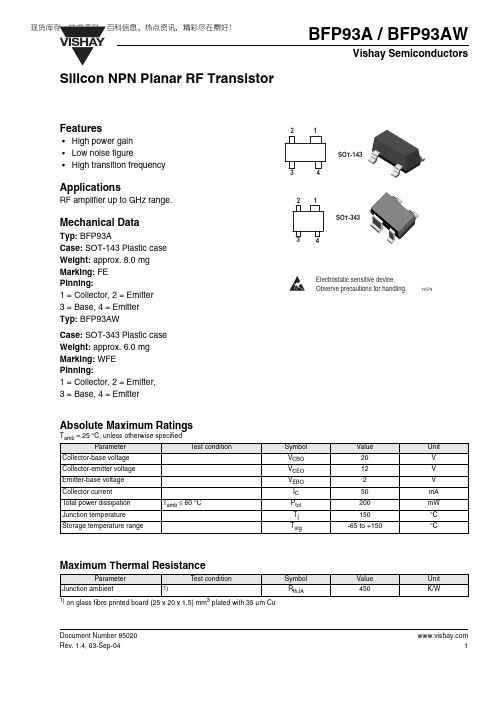
BFP93A / BFP93AWDocument Number 85020Vishay SemiconductorsSilicon NPN Planar RF TransistorFeatures•High power gain •Low noise figure•High transition frequencyApplicationsRF amplifier up to GHz range.Mechanical DataTyp: BFP93ACase: SOT-143 Plastic case Weight: approx. 8.0 mg Marking: FE Pinning:1 = Collector,2 = Emitter3 = Base,4 = Emitter Typ: BFP93AWCase: SOT-343 Plastic case Weight: approx. 6.0 mg Marking: WFE Pinning:1 = Collector,2 = Emitter,3 = Base,4 = EmitterAbsolute Maximum RatingsT amb = 25°C, unless otherwise specifiedMaximum Thermal Resistance1) on glass fibre printed board (25 x 20 x 1.5) mm 3 plated with 35 µm CuParameterTest conditionSymbol Value Unit Collector-base voltage V CBO 20V Collector-emitter voltage V CEO 12V Emitter-base voltage V EBO 2V Collector current I C 50mA Total power dissipation T amb ≤ 60°CP tot 200mW Junction temperature T j 150°C Storage temperature rangeT stg-65 to +150°CParameterTest condition Symbol Value Unit Junction ambient1)R thJA450K/W Document Number 85020BFP93A / BFP93AWVishay Semiconductors Electrical DC CharacteristicsT amb = 25°C, unless otherwise specifiedElectrical AC CharacteristicsT amb = 25°C, unless otherwise specifiedParameterTest conditionSymbol MinT yp.Max Unit Collector-emitter cut-off current V CE = 20 V , V BE = 0I CES 100µA Collector-base cut-off current V CB = 15 V , I E = 0I CBO 100nA Emitter-base cut-off current V EB = 2 V , I C = 0I EBO 10µA Collector-emitter breakdown voltageI C = 1 mA, I B = 0V (BR)CEO 12V Collector-emitter saturation voltageI C = 50 mA, I B = 5 mAV CEsat 0.10.4VDC forward current transfer ratio V CE = 5 V , I C = 30 mAh FE4090150ParameterTest conditionSymbol MinT yp.MaxUnit Transition frequency V CE = 5 V , I C = 30 mA, f = 500 MHzf T 6GHz Collector-base capacitance V CB = 10 V , f = 1 MHz C cb 0.45pF Collector-emitter capacitance V CE = 10 V , f = 1 MHz C ce 0.2pF Emitter-base capacitance V EB = 0.5 V , f = 1 MHz C eb 1.25pF Noise figureV CE = 8 V , Z S = 50 Ω, f = 800 MHz, I C = 5 mA F 1.6dB V CE = 8 V , Z S = 50 Ω, f = 800 MHz, I C = 25 mAF 2.1dB Power gainV CE = 8 V , Z S = 50 Ω, Z L = Z Lopt , I C = 25 mA, f = 800 MHz G pe 17dB V CE = 8 V , Z S = 50 Ω, Z L = Z Lopt , I C = 25 mA, f = 2 GHzG pe 10dB Linear output voltage - two tone intermodulation test V CE = 8 V , I C = 25 mA, d IM = 60 dB, f 1 = 806 MHz,f 2 = 810 MHz, Z S = Z L = 50 ΩV 1 = V 2260mVThird order intercept pointV CE = 8 V , I C = 25 mA, f = 800 MHzIP 331dBmBFP93A / BFP93AWDocument Number 85020Vishay SemiconductorsCommon Emitter S-ParametersZ 0 = 50 Ω, T amb = 25°C, unless otherwise specified V CE /VI C /mAf/MHzS11S21S12S22LIN MAGANG LIN MAGANG LIN MAGANG LIN MAGANG deg deg deg deg 3101000.642-64.022.49143.10.02661.30.797-31.53000.566-130.112.29109.60.04543.50.433-52.75000.555-156.28.0095.50.05342.70.293-54.68000.560-176.6 5.2582.40.06645.50.221-52.710000.567173.8 4.3075.80.07546.60.204-52.612000.580166.3 3.6469.30.08547.00.192-54.215000.601156.6 2.9760.20.09946.60.181-60.018000.620148.0 2.5252.10.11245.60.171-68.020000.642143.3 2.3046.60.12244.60.170-74.422000.662137.5 2.1341.50.13243.50.169-79.825000.691130.2 1.9033.40.14337.90.168-92.428000.715123.1 1.7025.90.15237.70.176-104.230000.733119.4 1.5921.60.16036.40.180-112.73301000.486-114.234.23127.80.01756.00.600-48.73000.552-162.214.5699.70.02955.00.248-67.85000.563-177.29.1089.10.04059.70.149-66.78000.572169.7 5.8478.50.05862.00.105-59.310000.578162.6 4.7572.60.07161.40.098-57.012000.590157.0 4.0167.00.08460.00.093-58.515000.609149.7 3.2558.40.10157.50.090-67.518000.631142.5 2.7651.00.11754.40.086-80.220000.649138.7 2.5045.90.12952.10.089-90.022000.673133.3 2.3141.00.14050.00.091-97.425000.698126.9 2.0633.30.15143.70.099-116.428000.718120.6 1.8426.50.16242.20.112-129.830000.736116.6 1.7221.90.16940.30.124-138.55101000.658-59.422.80144.70.02462.30.816-28.23000.557-125.312.81111.00.04244.40.468-46.65000.538-152.88.4296.60.05043.30.331-46.88000.543-174.4 5.5183.30.06245.80.263-44.010000.546175.6 4.5076.60.07147.40.248-43.812000.561167.7 3.8270.20.08047.60.237-45.115000.578157.8 3.1261.10.09347.40.225-50.018000.601149.0 2.6553.20.10546.70.215-56.520000.623143.9 2.4147.70.11546.00.213-61.822000.640138.2 2.2342.60.12445.00.211-66.525000.673131.0 1.9934.70.13639.40.206-77.428000.696123.9 1.7927.00.14439.30.208-87.930000.709119.6 1.6822.70.15138.00.208-95.75301000.483-104.735.46129.20.01657.30.625-43.0 Document Number 85020BFP93A / BFP93AWVishay Semiconductors3000.519-157.715.38100.30.02855.00.276-54.35000.525-174.09.6389.20.03959.20.184-47.08000.531172.2 6.2178.40.05761.30.153-36.710000.527165.0 5.0572.50.06960.90.151-34.612000.534159.5 4.2866.50.08159.40.149-35.215000.547151.1 3.5057.70.09956.30.145-40.718000.561143.1 2.9849.80.11552.80.138-48.220000.570138.1 2.7244.20.12750.30.138-55.222000.587131.9 2.5338.90.13947.90.139-60.925000.601123.8 2.2730.10.15440.80.129-75.228000.619114.4 2.0722.30.16538.40.136-87.830000.628108.4 1.9517.20.17435.40.140-98.5851000.807-37.814.08154.20.02669.90.906-17.33000.646-94.19.77121.80.05445.80.656-33.85000.573-126.8 6.93104.30.06537.90.510-37.18000.549-155.7 4.7088.50.07334.70.423-38.210000.544-168.8 3.8980.80.07834.40.399-39.012000.555-179.3 3.3273.50.08334.80.382-40.715000.572168.6 2.7363.60.09035.30.367-44.718000.591157.8 2.3455.00.09836.30.356-50.220000.613151.4 2.1449.10.10436.30.352-54.522000.631144.3 1.9843.50.11036.30.349-58.425000.649135.2 1.7735.20.11935.80.347-65.328000.677126.9 1.6027.30.12635.70.351-74.630000.695122.6 1.5022.80.13234.90.345-80.88101000.687-54.722.73146.00.02363.50.827-25.93000.551-119.413.13112.30.04145.20.494-42.95000.520-148.48.6897.30.04843.80.360-42.58000.519-171.6 5.7084.00.06146.10.294-39.810000.523178.3 4.6677.30.06947.20.279-39.712000.534170.0 3.9570.80.07847.50.268-40.915000.551159.6 3.2261.70.09147.30.255-45.318000.575151.4 2.7453.80.10346.20.244-51.420000.598146.1 2.5048.30.11245.60.241-56.322000.617140.0 2.3143.10.12044.60.238-60.425000.641132.3 2.0635.20.13339.40.231-69.928000.672125.4 1.8427.80.13939.10.231-79.730000.687121.6 1.7323.40.14637.90.226-87.08151000.606-68.328.45140.30.02060.80.764-31.7V CE /VI C /mAf/MHzS11S21S12S22LIN MAGANG LIN MAGANG LIN MAGANG LIN MAGANG deg deg deg degBFP93A / BFP93AWDocument Number 85020Vishay Semiconductors3000.520-133.814.66107.50.03547.70.408-47.25000.506-158.79.4394.20.04349.10.289-44.58000.510-178.4 6.1382.10.05752.60.236-39.710000.515172.5 5.0075.80.06753.50.227-39.212000.530165.1 4.2269.80.07753.40.219-40.015000.550156.5 3.4361.00.09252.20.209-44.918000.573148.2 2.9153.50.10650.00.199-51.520000.586143.5 2.6548.10.11548.90.196-56.822000.614137.7 2.4443.20.12547.70.194-61.125000.644131.1 2.1935.40.13841.10.185-72.628000.667124.1 1.9528.20.14441.00.186-82.730000.680120.2 1.8424.20.15239.50.184-90.88201000.558-79.532.26136.20.01858.50.714-35.73000.509-143.115.46104.70.03150.30.356-49.45000.502-165.39.8192.40.04053.30.249-45.38000.511177.7 6.3381.00.05656.70.205-39.010000.517169.2 5.1675.10.06757.00.199-38.112000.527162.4 4.3669.10.07756.60.193-39.215000.546154.4 3.5460.70.09255.00.184-44.518000.568146.5 2.9953.10.10752.30.175-51.620000.591142.2 2.7348.10.11750.90.173-57.222000.610136.8 2.5143.00.12749.20.170-61.925000.639130.4 2.2435.50.14042.40.163-74.828000.665123.2 2.0128.50.14742.10.164-85.230000.684119.9 1.8924.50.15440.50.162-94.38251000.525-88.234.79133.10.01758.00.676-38.53000.505-148.915.91102.80.02952.50.322-50.85000.503-168.810.0191.20.03956.30.224-45.28000.511175.1 6.4380.20.05559.30.187-37.010000.518167.2 5.2474.30.06659.50.183-36.912000.528161.0 4.4268.60.07858.40.178-38.215000.548153.2 3.5960.30.09356.30.170-43.718000.571145.9 3.0352.90.10853.60.161-51.220000.585141.5 2.7647.80.11851.80.159-57.322000.613136.0 2.5543.10.12850.00.157-62.125000.642129.6 2.2735.30.14143.40.150-75.728000.669122.7 2.0428.50.14842.70.151-86.730000.683119.4 1.9124.20.15640.90.151-96.28301000.507-95.136.47130.80.01657.90.644-46.6V CE /VI C /mAf/MHzS11S21S12S22LIN MAGANG LIN MAGANG LIN MAGANG LIN MAGANG deg deg deg deg Document Number 85020BFP93A / BFP93AWVishay SemiconductorsTypical Characteristics (T amb = 25 °C unless otherwise specified)3000.506-153.116.13101.40.02754.40.299-51.25000.506-171.510.1090.40.03658.70.208-44.58000.515173.2 6.4879.60.05561.10.176-36.710000.523166.1 5.2874.00.06660.90.173-35.712000.531159.9 4.4568.20.07760.00.169-37.015000.551152.4 3.6059.90.09357.40.162-42.718000.574145.2 3.0552.70.10854.40.154-50.820000.585141.0 2.7647.40.11952.60.152-56.922000.613135.7 2.5742.80.12850.80.150-62.025000.644129.2 2.2835.10.14143.90.143-76.228000.669122.8 2.0428.50.14943.20.145-87.630000.685119.21.9124.20.15641.40.144-97.7V CE /VI C /mAf/MHzS11S21S12S22LIN MAGANG LIN MAGANG LIN MAGANG LIN MAGANG deg deg deg deg Figure 1. Total Power Dissipation vs. Ambient Temperature Figure 2. Transition Frequency vs. Collector Current 0501001502002503000204060801001201401609612159P -T o t a l P o w e r D i s s i p a t i o n (m W )t o t T amb -Ambient T emperature (°C )010002000300040005000600070001020304050I C –Collector Current (mA )12880f –T r a n s i t i o n F r e q u e n c y (M H z )T Figure 3. Collector Base Capacitance vs. Collector Base VoltageFigure 4. Noise Figure vs. Collector Current0.00.20.40.60.81.0048121620V CB –Collector Base Voltage (V )12881C –C o l l e c t o r B a s e C a p a c i t a n c e (p F )c b 01234510152025I C –Collector Current (mA )12882F –N o i s e F i g u r e (d B )BFP93A / BFP93AWDocument Number 85020Vishay SemiconductorsV CE = 8 V, I C = 30 mA, Z 0 = 50 ΩS 11S 12S 21S 22Figure 5. Input Reflection Coefficient Figure 6. Reverse Transmission Coefficient 12990ı∞129910°180°°°Figure 7. Forward Transmission CoefficientFigure 8. Output Reflection Coefficient129920°180°°°129930jı∞ Document Number 85020BFP93A / BFP93AWVishay Semiconductors Package Dimensions in mmPackage Dimensions in mmBFP93A / BFP93AWDocument Number 85020Vishay SemiconductorsOzone Depleting Substances Policy StatementIt is the policy of Vishay Semiconductor GmbH to1.Meet all present and future national and international statutory requirements.2.Regularly and continuously improve the performance of our products, processes, distribution andoperatingsystems with respect to their impact on the health and safety of our employees and the public, as well as their impact on the environment.It is particular concern to control or eliminate releases of those substances into the atmosphere which are known as ozone depleting substances (ODSs).The Montreal Protocol (1987) and its London Amendments (1990) intend to severely restrict the use of ODSs and forbid their use within the next ten years. Various national and international initiatives are pressing for an earlier ban on these substances.Vishay Semiconductor GmbH has been able to use its policy of continuous improvements to eliminate the use of ODSs listed in the following documents.1.Annex A, B and list of transitional substances of the Montreal Protocol and the London Amendments respectively2.Class I and II ozone depleting substances in the Clean Air Act Amendments of 1990 by the Environmental Protection Agency (EPA) in the USA3.Council Decision 88/540/EEC and 91/690/EEC Annex A, B and C (transitional substances) respectively.Vishay Semiconductor GmbH can certify that our semiconductors are not manufactured with ozone depleting substances and do not contain such substances.We reserve the right to make changes to improve technical designand may do so without further notice.Parameters can vary in different applications. All operating parameters must be validated for each customer application by the customer. Should the buyer use Vishay Semiconductors products for any unintended or unauthorized application, the buyer shall indemnify Vishay Semiconductors against all claims, costs, damages, and expenses, arising out of, directly or indirectly, any claim of personaldamage, injury or death associated with such unintended or unauthorized use.Vishay Semiconductor GmbH, P.O.B. 3535, D-74025 Heilbronn, GermanyTelephone: 49 (0)7131 67 2831, Fax number: 49 (0)7131 67 2423。
ms934芯片手册

MS934芯片手册引言概述:本文旨在介绍MS934芯片,并提供详细的技术手册,以帮助读者更好地了解和使用该芯片。
MS934芯片是一款高性能的集成电路芯片,广泛应用于各种电子设备中。
通过本手册,读者将能够深入了解MS934芯片的功能特性、应用场景、工作原理等相关内容。
正文内容:1. MS934芯片的基本概述1.1 芯片的封装类型MS934芯片通常采用LQFP封装,方便安装和布局,同时具有良好的散热性能。
LQFP封装还提供了丰富的IO引脚数量和外部扩展接口,方便用户在应用中进行灵活连接。
1.2 芯片的主要功能MS934芯片具备高性能的处理器单元和丰富的外设功能,可提供多种功能实现的可能。
芯片内部集成了高速时钟电路、存储器控制器以及多种数字接口,能够满足复杂系统的需求。
1.3 芯片的主要规格参数内建8MB的Flash存储器和512KB的RAM,可支持大容量程序和数据存储。
工作频率可达200 MHz,提供强大的计算和处理能力。
支持多种数字接口,如UART、SPI、I2C等,满足不同的外设连接需求。
2. MS934芯片的应用场景2.1 智能家居领域MS934芯片能够提供稳定且高效的智能家居系统控制能力。
通过与各类传感器连接,实现对家庭环境的自动感知和调节,提升居住舒适度。
芯片的高性能处理能力和丰富的接口资源,可以满足智能家居中的复杂计算和通信需求。
2.2 工业自动化领域MS934芯片具备强大的实时控制能力和高速数据处理能力,非常适合用于工业自动化系统。
芯片支持多种高速通信接口,如以太网、CAN总线等,可实现与各类工控设备的联网。
同时,芯片提供了丰富的GPIO接口和模拟输入输出接口,方便连接和控制各类工业传感器和执行器。
2.3 汽车电子领域MS934芯片的高性能和可靠性使其成为汽车电子领域的理想选择。
芯片采用了低功耗设计,适应汽车电子系统对能效和环境适应性的要求。
可扩展的IO接口和丰富的外设功能,使芯片能够满足复杂的汽车电子系统集成和控制需求。
TPI 精确度194多功能数字多元器说明书
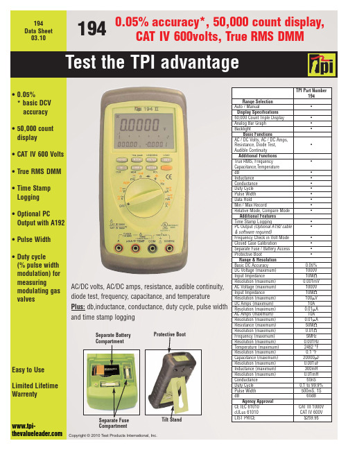
Test the TPI advantageCopyright © 2010 Test Products International, Inc.194 Data Sheet 03.100.05% accuracy*, 50,000 count display,CAT IV 600volts, True RMS DMM194•0.05%*basic DCV accuracy •50,000 count display •CAT IV 600 Volts •True RMS DMM •Time Stamp Logging •Optional PC Output with A192•Pulse Width •Duty cycle (% pulse width modulation) for measuring modulating gas valvesAC/DC volts, AC/DC amps, resistance, audible continuity,diode test, frequency, capacitance, and temperaturePlus:db,inductance, conductance, duty cycle, pulse width and time stamp loggingEasy to Use Limited Lifetime WarrentySeparate Battery CompartmentSeparate Fuse CompartmentTilt StandProtective BootTPI Part Number194Range Selection Auto / Manual •Display Specifications 50,000 Count Triple Display •Analog Bar Graph •Backlight •Basic FunctionsAC / DC Volts, AC / DC Amps,Resistance, Diode Test,•Audible ContinuityAdditional Functions True RMS, Frequency •Capacitance,Temperature dB •Inductance •Conductance •Duty Cycle •Pulse Width •Data Hold •Min / Max Record •Relative Mode, Compare Mode •Additional Features Time Stamp Logging •PC Output (Optional A192 cable•& software required)Frequency Check in Volt Mode •Closed Case Calibration •Separate Fuse / Battery Access •Protective Boot •Range & Resolution Basic DC Accuracy 0.05% DC Voltage (maximum)1000V Input Impedance 10M Resolution (maximum)0.001mV AC Voltage (maximum)1000V Input Impedance 10M Resolution (maximum)100 V DC Amps (maximum)10A Resolution (maximum)0.01 A AC Amps (maximum)10A Resolution (maximum)0.01 A Resistance (maximum)50M Resolution (maximum)0.01 Frequency (maximum)5MHz Resolution (maximum)0.001Hz Temperature (maximum)2462 °F Resolution (maximum)0.1 °F Capacitance (maximum)20000 F Resolution (maximum)0.001uF Inductance (maximum)300mH Resolution (maximum)0.01mH Conductance 50nS Duty Cycle 0.1 to 99.9%Pulse Width 500mS, 1S dB 60dBAgency Approval CE IEC 61010CAT III 1000V cULus 61010CAT IV 600V LIST PRICE $259.95Photo is actual size With Protective Boot 8.7 x 4.3 x 2.6REC:Display the minimum, maximum, and average readingbeing measuredDIODE TEST :Displays approximate forward bias voltage of a diodeCOMP : Compare a measured value to a manually entered valuePC OUTPUT:Isolated optical to USB output (Optional A192cable & software required)TRIPLE DISPLAY:Shows more information simultaneouslyREL%: Display measured values relative to a stored value and as a percentage of the stored valueEDIT: Used when manually entering valuesHOLD : Freezes measured valueson the displayFunction Key:Select between multiple functions at each selector position.ADP : Selector position when using optional accessory adapters •A254 low AC/DC amp clamp • A256 AC/DC amp clamp•A296 high AC/DC amp clamp •A620 pressure adapterLarge 50,000count display with bargraphRANGE:Select between auto and manual rangingBACKLIGHT :Allows viewing in low light conditionsTPI 194 comes with:• A085silicone test leads with alligator clips• A106 temperature input adapter • GK11M beaded K-typetemperature probe RESISTANCE,CONTINUITY &BUZZER。
L9311资料

The Agere Systems Inc. L9311 is a combination fullfeature, ultralow-power SLIC, solid-state ringing access relay, and line test matrix. It is part of a pinfor-pin compatible family of devices designed to serve a wide variety of applications. The L9311 is optimized for North American access applications where TR-57 longitudinal balance and GR-909 line test are required.
L9311 Full-Feature SLIC with High Longitudinal Balance, Ringing Relay, and GR-909 Test Access
Data Sheet July 2001
Table of Contents
Contents Page Contents Page
Introduction..................................................................1 Features ....................................................................1 SLIC .......................................................................1 Solid-State Ring Relay ...........................................1 Line Test Matrix......................................................1 Applications...............................................................1 Description ................................................................1 Features ......................................................................4 Description...................................................................4 Architecture .................................................................8 Pin Information ............................................................9 Operating States........................................................11 Input State Coding ..................................................11 State Definitions ........................................................13 Primary Control Modes ...........................................13 Powerup, Forward Battery....................................13 Powerup, Reverse Battery ...................................13 Scan .....................................................................13 Ground Start.........................................................13 Ringing .................................................................13 Disconnect—Break Before Make .........................14 Tip Amp ................................................................14 Ring Amp .............................................................14 Tip and Ring Amp.................................................14 Reset ....................................................................14 Secondary Control Mode States .............................14 Voltage: Tip to Ground .........................................14 Voltage: Ring to Ground.......................................14 Voltage: Tip to Ring..............................................14 Current: Tip to Ring—VTX ...................................14 Current: Tip to Ring—VITR ..................................15 Reference Voltage ...............................................15 TEST Off ..............................................................15 Special States .........................................................15 Thermal Shutdown ...............................................15 Battery Out of Range ...........................................15 Absolute Maximum Ratings.......................................16 Electrical Characteristics ...........................................17 Ring Trip Detector ...................................................18 Test ........................................................................19 SLIC Two-Wire Port ................................................20 Analog Pin Characteristics ......................................21 ac Feed Characteristics ..........................................22 Logic Inputs and Outputs, VDD = 5.0 V ...................23 Timing Requirements ..............................................23 Switch Characteristics.............................................24 On-State Switch I-V Characteristics........................25 Test Configurations ...................................................26
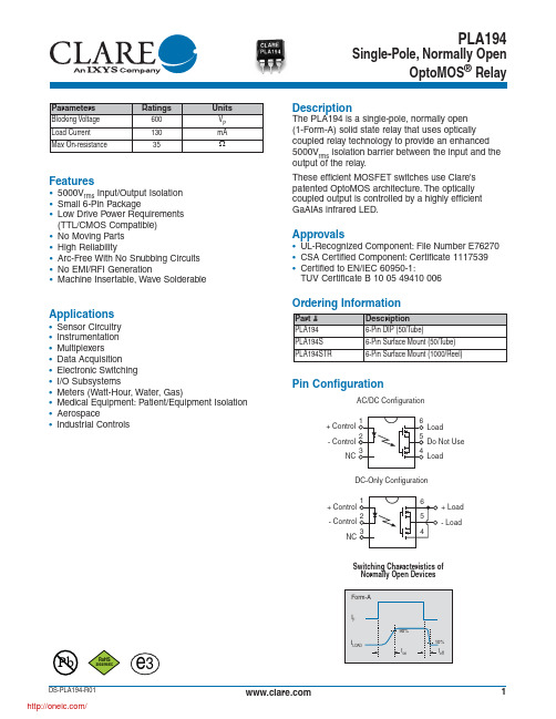
PLA194STR;中文规格书,Datasheet资料
Device Count (N)
0.34 0.37 0.40 0.43 0.46 0.49 0.52 0.55 Turn-Off Time (ms)
20
Typical IF for Switch Operation (N=50, IL=130mA, TA=25ºC)
25 20 15 10 5 0
Typical On-Resistance Distribution (N=50, IF=2mA, IL=130mA, TA=25ºC)
Ω μA
IF=5mA, VL=10V VL=50V, f=1MHz IL=130mA IF=5mA VR=5V -
ms pF mA mA V μA pF
Load current derates linearly from 130mA @ 25ºC to 65mA @ 85ºC. 2 Measurement taken within 1 second of on-time. 3 For applications requiring high temperature operation (greater than 60ºC), a LED drive current of 3mA is recommended.
1
Conditions
Symbol
Min
Typ
Max
Units
t=10ms IL=130mA IL=200mA VL=600VP
IL ILPK
0.1 0.9 -
26 0.85 0.46 5 0.44 1.2 3
130 200 400 35 18 1 3 2 2 1.4 10 -
mA
RON ILEAK ton toff COUT IF IF VF IR CI/O
LMBTA43LT1G资料

元器件交易网
hFE , DC CURRENT GAIN
C, CAPACITANCE (pF)
LESHAN RADIO COMPANY, LTD. LMBTA42LT1 LMBTA43LT1
200
V CE= 10Vdc
T J = 125°C
100
25°C
50
– 55°C
30
Characteristic
Symbol
Min
Max
Unit
OFF CHARACTERISTICS
Collector–Emitter Breakdown Voltage(3)
(I C = 1.0 mAdc, I B = 0)
LMBTA42 LMBTA43
Collector–Base Breakdown Voltage (I C= 100 µAdc, I E= 0)
LMBTA42 LMBTA43
Emitter–Base Breakdown Voltage (I E= 100 µAdc, I C= 0) Collector Cutoff Current
( V CB= 200Vdc, I E= 0) ( V CB= 160Vdc, I E= 0) Emitter Cutoff Current
LESHAN RADIO COMPANY, LTD.
LMBTA42LT1 LMBTA43LT1
A L
3
BS
1
2
V
G
C
D
H K
SOT-23
J
NOTES: 1. DIMENSIONING AND TOLERANCING PER ANSI
Y14.5M, 1982. 2. CONTROLLING DIMENSION: INCH.
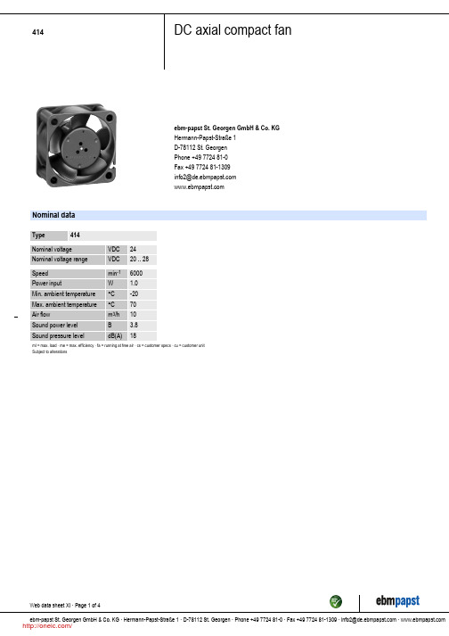
414;中文规格书,Datasheet资料
/
414
DC axial compact fan
Product drawing
Web data sheet XI · Page 3 of 4 ebm-papst St. Georgen GmbH & Co. KG · Hermann-Papst-Straße 1 · D-78112 St. Georgen · Phone +49 7724 81-0 · Fax +49 7724 81-1309 · info2@ ·
Mass Dimensions Material of impeller Housing material Direction of air flow Direction of rotation Bearing Lifetime L10 at 20 °C Lifetime L10 at 60 °C Connection line Motor protection Approval
/
分销商库存信息:
EBM-PAPST 414
/
414
DC axial compact fan
Technical features
General description Particular design features: Compact fan with low power consumption. Some models suitable for use at high ambient temperatures. General features: Material: fibreglass-reinforced plastic. Impeller PA, housing PBT. Electronic commutation completely integrated. Protected against reverse polarity and locking. Connection via single strands AWG 28, TR 64, bared and tin-plated. Air exhaust over bars. Direction of rotation counter-clockwise seen on rotor. Masse: 17 g. 0.027 kg 40 x 40 x 20 mm Fiberglass-reinforced PA plastic Fiberglass-reinforced PBT plastic Air exhaust over bars Left, looking at rotor Sintec sleeve bearing 50000 h 20000 h Single strands AWG 28, TR 64, bared and tin-plated. Protected against reverse polarity and locking. VDE, CSA, UL
ATF34143中文资料
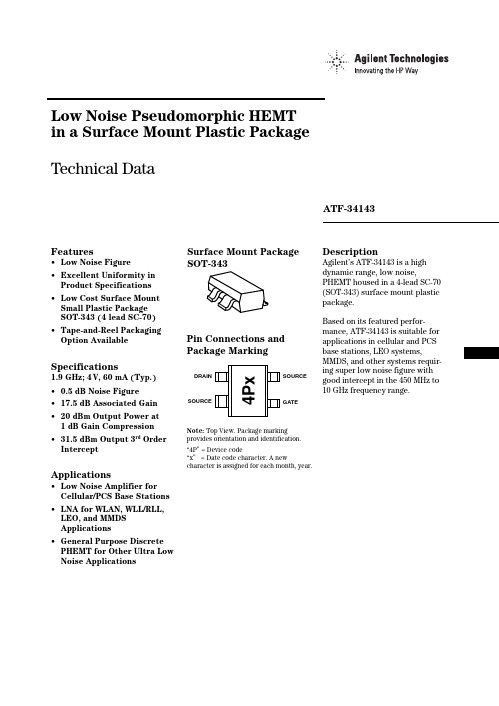
+3 Std
60 40 20 0 16
-3 Std
+3 Std
0.6
0.8
16.5
17
17.5
18
18.5
19
GAIN (dB)
Figure 3. NF @ 2 GHz, 4 V, 60 mA. LSL=0.1, Nominal=0.47, USL=0.8
Figure 4. Gain @ 2 GHz, 4 V, 60 mA. LSL=16.0, Nominal=17.5, USL=19.0
Circuit losses have been de-embedded from actual measurements.
ATF-34143 Electrical Specifications
TA = 25°C, RF parameters measured in a test circuit for a typical device Symbol Idss [1] VP [1] Id gm[1] IGDO Igss NF Parameters and Test Conditions Saturated Drain Current VDS = 1.5 V, VGS = 0 V Pinchoff Voltage VDS = 1.5 V, IDS = 10% of Idss Quiescent Bias Current VGS = 0.34 V, VDS = 4 V Transconductance VDS = 1.5 V, gm = Idss /VP Gate to Drain Leakage Current VGD = 5 V Gate Leakage Current VGD = VGS = -4 V Noise Figure f = 2 GHz VDS = 4 V, IDS = 60 mA VDS = 4 V, IDS = 30 mA f = 900 MHz VDS = 4 V, IDS = 60 mA Associated Gain f = 2 GHz VDS = 4 V, IDS = 60 mA VDS = 4 V, IDS = 30 mA f = 900 MHz VDS = 4 V, IDS = 60 mA rd Order Output 3 f = 2 GHz VDS = 4 V, IDS = 60 mA Intercept Point [3] +5 dBm Pout /Tone VDS = 4 V, IDS = 30 mA f = 900 MHz VDS = 4 V, IDS = 60 mA +5 dBm Pout /Tone 1 dB Compressed f = 2 GHz VDS = 4 V, IDS = 60 mA Intercept Point [3] VDS = 4 V, IDS = 30 mA f = 900 MHz VDS = 4 V, IDS = 60 mA Units mA V mA mmho µA µA dB dB dB dB dBm dBm dBm dBm Min. Typ.[2] 90 118 -0.65 -0.5 — 60 180 230 — 30 0.5 0.5 0.4 17.5 17 21.5 31.5 30 31 20 19 18.5 Max. 145 -0.35 — — 500 300 0.8
AG9311中文规格说明书2020新版.PDF
AG9311带PD3.0 Type C转HDMI转换器AG9311AG9311Type-C转HDMI转换器数据表修订历史PS:本中文规格书由第三方翻译软件自动翻译,权威信息请以原厂英文版规格书为准。
2AG9311Type-C转HDMI转换器数据表索引1.概述 (5)2.特性 (5)3.设备信息 (6)4.应用 (6)5.系统框图 (7)6.管脚映射和描述 (8)7.规格明细 (15)i. 绝对最大额定值绝对最大额定值 (15)ii. 直流特性/工作条件 (15)iii. 交流特性 (16)8. 包装和标记规范 (19)3AG9311Type-C转HDMI转换器数据表图目录图1 Type-C转HDMI 适配器的应用 (6)图2系统框图 (7)图3 AG9311MAQ引脚映射 (8)图4 AG9311-MCQ引脚映射 (12)图5 AG9311-MAQ包装尺寸..... (20)图6 AG9311-MCQ包装尺寸 (21)表格列表表1引脚说明........ (9)表2引脚说明....... (12)表3绝对最大额定值 (15)表4数字I/O规范.... (16)表5显示端口输入 (16)表6显示端口辅助通道I/O规格. (17)表7 USB I/O规格 (18)表8 USB PD规格 (18)4AG9311Type-C转HDMI转换器数据表一、概述ALGOLTEK AG9311是一款高度集成的解决方案,通过USB Type-C将视频和音频从DisplayPort alternate mode传输到HDMI输出。
AG9311支持各种@1.62Gbps、2.7Gbps和5.4Gbpsup通到DisplayPort 1.2,支持1路2路通道;HDMI支持4K/2K@30Hz输出。
用户可以轻松地将AG9311集成到视频转换适配器和扩展坞上。
二、特性1、显示符合 DisplayPort specification Revision 1.2支持1.62(RBR)/2.7(HBR)/5.4(HBR2)Gbps数据速率支持1/2线路配置支持下行扩频时钟(SSC)-支持I2S总线音频提取2、HDMIHDMI 高清多媒体接口符合HDMI1.4和HDCP1.4规范支持高达3Gbps的TMD支持分辨率高达4kx2k@30Hz输出支持HDCP键预先编程兼容EDID和MCCS支持采样率48kHz/44.1KHz/32KHz的LPCM双通道3、USB Type-C PD支持显示端口备用模式协议DisplayPort Alternate符合USB PD3.0集成Type-C RP and RD电阻器支持2个 USB Type-C端口支持USB宣称集成USB2.0全速5AG9311Type-C转HDMI转换器数据表4、单片机系统及接口集成16位单片机集成用于固件升级的64KB闪存支持I2C主/从、UART、USB2.0全速支持3通道8 bit分辨率ADC5、电源操作和ESD3.3V:3V至3.6V操作1.2V:1.08至1.32V运行1.2V核心电源和3.3V I/O电源HBM 2KV ESD性能三、设备信息四、应用USB Type-C 转换器USB Type-C扩展坞6AG9311Type-C转HDMI转换器数据表五、系统框图7AG9311Type-C转HDMI转换器数据表六、管脚映射和描述图3 AG9311-MAQ引脚映射8AG9311Type-C转HDMI转换器数据表表1基本说明9AG9311Type-C转HDMI转换器数据表10AG9311Type-C转HDMI转换器数据表11AG9311Type-C转HDMI转换器数据表图4 AG9311-MCQ引脚映射表2引脚说明12AG9311 Type-C转HDMI转换器数据表13AG9311 Type-C转HDMI转换器数据表14AG9311Type-C转HDMI转换器数据表七、规格明细1.绝对最大额定值表3绝对最大额定值2.直流特性/工作条件15AG9311Type-C转HDMI转换器数据表Table 4 Digital I/O Specification表4数字I/O规范3.交流特性显示端口主链交流特性表5显示端口输入定时16AG9311Type-C转HDMI转换器数据表显示端口AUX-CH AC特性表6显示端口辅助通道I/O规格17AG9311Type-C转HDMI转换器数据表USB PD BMC接收器规范要求表7 USB I/O规格USB PD BMC发射机规范要求表8 USB PD规格AG9311Type-C转HDMI转换器数据表八、包装和标记规范标记19AG9311Type-C转HDMI转换器数据表包装尺寸AG9311-MAQ: QFN-64L 8x8mm(E-PAD SIZE:181x18*MIL)图5 AG9311-MAQ包装尺寸20AG9311Type-C转HDMI转换器数据表AG9311-MCQ:QFN-48L 6x6mm(电子板尺寸:185x18*MIL)Figure 6 AG9311-MCQ Package Dimension图6 AG9311-MCQ包装尺寸21。
ADL8141 Data Sheet说明书
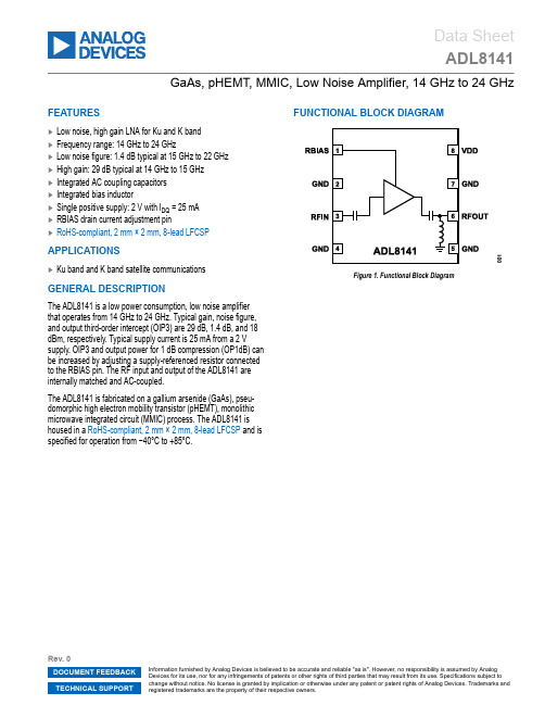
Data SheetADL8141GaAs, pHEMT, MMIC, Low Noise Amplifier, 14 GHz to 24 GHz FEATURES►Low noise, high gain LNA for Ku and K band►Frequency range: 14 GHz to 24 GHz►Low noise figure: 1.4 dB typical at 15 GHz to 22 GHz►High gain: 29 dB typical at 14 GHz to 15 GHz►Integrated AC coupling capacitors►Integrated bias inductor►Single positive supply: 2 V with I DQ = 25 mA►RBIAS drain current adjustment pin►RoHS-compliant, 2 mm × 2 mm, 8-lead LFCSP APPLICATIONS►Ku band and K band satellite communicationsGENERAL DESCRIPTIONThe ADL8141 is a low power consumption, low noise amplifier that operates from 14 GHz to 24 GHz. Typical gain, noise figure, and output third-order intercept (OIP3) are 29 dB, 1.4 dB, and 18 dBm, respectively. Typical supply current is 25 mA from a 2 V supply. OIP3 and output power for 1 dB compression (OP1dB) can be increased by adjusting a supply-referenced resistor connected to the RBIAS pin. The RF input and output of the ADL8141 are internally matched and AC-coupled.The ADL8141 is fabricated on a gallium arsenide (GaAs), pseu-domorphic high electron mobility transistor (pHEMT), monolithic microwave integrated circuit (MMIC) process. The ADL8141 is housed in a RoHS-compliant, 2 mm × 2 mm, 8-lead LFCSP and is specified for operation from −40°C to +85°C.FUNCTIONAL BLOCK DIAGRAMFigure 1. Functional Block DiagramTABLE OF CONTENTSFeatures (1)Applications (1)General Description (1)Functional Block Diagram (1)Specifications (3)14 GHz to 15 GHz Frequency Range (3)15 GHz to 22 GHz Frequency Range (3)22 GHz to 24 GHz Frequency Range (3)DC Specifications (4)Absolute Maximum Ratings (5)Thermal Resistance (5)Electrostatic Discharge (ESD) Ratings (5)ESD Caution.......................................................5Pin Configuration and Function Descriptions.. (6)Interface Schematics (6)Typical Performance Characteristics (7)Theory of Operation (18)Applications Information (19)Recommended Bias Sequencing (19)Using RBIAS as a Fast Enable and Disable Function (20)Recommended Power Management Circuit (21)Outline Dimensions (22)Ordering Guide (22)Evaluation Boards (22)REVISION HISTORY7/2023—Revision 0: Initial Version14 GH z TO 15 GH z FREQUENCY RANGESupply voltage (V DD) = 2 V, quiescent current (I DQ) = 25 mA, bias reference (R BIAS) = 768 Ω, and T C = 25°C, unless otherwise noted.Table 1. 14 GHz to 15 GHz Frequency Range SpecificationsParameter Min Typ Max Unit Test Conditions/CommentsFREQUENCY RANGE1415GHzGAIN2729dBGain Variation over Temperature0.025dB/°CNOISE FIGURE 1.7dBRETURN LOSSInput (S11)12.5dBOutput (S22)7dBOUTPUTOP1dB 3.56dBmSaturated Output Power (P SAT)9dBmOIP311dBm Measurement taken at output power (P OUT) per tone =−2 dBmSecond-Order Intercept (OIP2)8.5dBm Measurement taken at P OUT per tone = −2 dBm15 GH z TO 22 GH z FREQUENCY RANGEV DD = 2 V, I DQ = 25 mA, R BIAS = 768 Ω, and T C = 25°C, unless otherwise noted.Table 2. 15 GHz to 22 GHz Frequency Range SpecificationsParameter Min Typ Max Unit Test Conditions/CommentsFREQUENCY RANGE1522GHzGAIN26.528.5dBGain Variation over Temperature0.024dB/°CNOISE FIGURE 1.4dBRETURN LOSSS1115dBS2212dBOUTPUTOP1dB69dBmP SAT11.5dBmOIP318dBm Measurement taken at P OUT per tone = −2 dBmOIP223dBm Measurement taken at P OUT per tone = −2 dBm22 GH z TO 24 GH z FREQUENCY RANGEV DD = 2 V, I DQ = 25 mA, R BIAS = 768 Ω, and T C = 25°C, unless otherwise noted.Table 3. 22 GHz to 24 GHz Frequency Range SpecificationsParameter Min Typ Max Unit Test Conditions/CommentsFREQUENCY RANGE2224GHzGAIN26dBGain Variation over Temperature0.033dB/°CNOISE FIGURE 1.5dBRETURN LOSSS1113.5dBS225dBTable 3. 22 GHz to 24 GHz Frequency Range Specifications (Continued)Parameter Min Typ Max Unit Test Conditions/CommentsOUTPUTOP1dB11dBmP SAT12dBmOIP317dBm Measurement taken at P OUT per tone = −2 dBm OIP231dBm Measurement taken at P OUT per tone = −2 dBmDC SPECIFICATIONSTable 4. DC SpecificationsParameter Min Typ Max Unit SUPPLY CURRENTI DQ25mA Amplifier Current (I DQ_AMP)23mA RBIAS Current (I RBIAS)2mA SUPPLY VOLTAGEV DD 1.52 3.5VABSOLUTE MAXIMUM RATINGSTable 5. Absolute Maximum RatingsParameter RatingV DD 4 VRF Input Power (RFIN)20 dBm Pulsed RFIN (Duty Cycle = 10%, Pulse Width = 100 μs)22 dBm Continuous Power Dissipation (P DISS), T CASE = 85°C(Derate 5.71 mW/°C Above 85°C)0.51 W TemperatureStorage Range−65°C to +150°C Operating Range−40°C to +85°C Quiescent Channel (T CASE = 85°C, V DD = 2 V, I DQ =25 mA, Input Power (P IN) = Off)93.75°CMaximum Channel175°CStresses at or above those listed under Absolute Maximum Ratings may cause permanent damage to the product. This is a stress rating only; functional operation of the product at these or any other conditions above those indicated in the operational section of this specification is not implied. Operation beyond the maximum operat-ing conditions for extended periods may affect product reliability. THERMAL RESISTANCEThermal performance is directly linked to printed circuit board (PCB) design and operating environment. Careful attention to PCB thermal design is required.θJC is the channel to case thermal resistance.Table 6. Thermal ResistancePackage TypeθJC UnitCP-8-30Quiescent, T CASE = 25°C 141°C/WWorst Case1, T CASE = 85°C 175°C/W 1Worst case across all specified operating conditions.ELECTROSTATIC DISCHARGE (ESD) RATINGS The following ESD information is provided for handling of ESD-sen-sitive devices in an ESD protected area only.Human body model (HBM) per ANSI/ESDA/JEDEC JS-001. ESD Ratings for ADL8141Table 7. ADL8141, 8-Lead LFCSPESD Model Withstand Threshold (V)ClassHBM±5001BESD CAUTIONPIN CONFIGURATION AND FUNCTION DESCRIPTIONSFigure 2. Pin ConfigurationTable 8. Pin Function Descriptions Pin No.Mnemonic Description1RBIAS Bias Setting Resistor. Connect a resistor between RBIAS and VDD to set the I DQ . See Figure 72 and Table 9 for more details. See Figure 3 for the interface schematic.2, 4, 5, 7GND Ground. Connect to a ground plane that has low electrical and thermal impedance. See Figure 6 for the interface schematic.3RFIN RF Input. The RFIN pin is AC-coupled and matched to 50 Ω. SeeFigure 4 for the interface schematic.6RFOUT RF Output. The RFOUT pin is AC-coupled and matched to 50 Ω. See Figure 5 for the interface schematic.8VDDDrain Bias. Connect the VDD pin to the supply voltage. See Figure 5 for the interface schematic.EXPOSED PADDLEExposed Ground Paddle. Connect the exposed paddle to a ground plane that has low electrical and thermal impedance.INTERFACE SCHEMATICSFigure 3. RBIAS Interface SchematicFigure 4. RFIN Interface SchematicFigure 5. RFOUT/VDD Interface SchematicFigure 6. GND Interface SchematicFigure 7. Broadband Gain and Return Loss vs. Frequency, V DD = 2 V,I DQ = 25 mAFigure 10. Gain vs. Frequency for Various Temperatures, V DD = 2 V,I DQ = 25 mA, R BIAS = 768 ΩFigure 13. Input Return Loss vs. Frequency for Various Supply Voltages andI DQ Values, R BIAS= 768 ΩFigure 14. Input Return Loss vs. Frequency for Various Supply Voltages andR BIAS Values, I DQ= 25 mAFigure 15. Output Return Loss vs. Frequency for Various Supply Voltagesand I DQ Values, R BIAS= 768 ΩFigure 16. Input Return Loss vs. Frequency for Various I DQ and R BIAS Values,V DD= 2 VFigure 17. Output Return Loss vs. Frequency for Various Temperatures, V DD= 2 V, I DQ = 25 mA, R BIAS= 768 ΩFigure 18. Output Return Loss vs. Frequency for Various I DQ and R BIASValues, V DD = 2 VFigure 19. Output Return Loss vs. Frequency for Various Supply Voltagesand R BIAS Values, I DQ= 25 mAFigure 20. Reverse Isolation vs. Frequency for Various Supply Voltages andI DQ Values, R BIAS= 768 ΩFigure 21. Reverse Isolation vs. Frequency forVarious Supply Voltages and R BIAS Values, I DQ= 25 mAFigure 22. Reverse Isolation vs. Frequency forVarious Temperatures, V DD = 2 V, I DQ = 25 mA, R BIAS= 768 ΩFigure 23. Reverse Isolation vs. Frequency for Various I DQ and R BIAS Values,V DD= 2 VFigure 24. Noise Figure vs. Frequency for Various Temperatures, V DD = 2 V,I DQ = 25 mA, R BIAS = 768 ΩFigure 25. Noise Figure vs. Frequency for Various Supply Voltages and I DQValues, R BIAS= 768 ΩFigure 26. Noise Figure vs. Frequency for Various Supply Voltages and R BIASValues, I DQ= 25 mAFigure 27. OP1dB vs. Frequency for Various Supply Voltages and I DQ Values,R BIAS= 768 ΩFigure 28. Noise Figure vs. Frequency for Various Supply Voltages and I DQValues, R BIAS= 768 ΩFigure 29. OP1dB vs. Frequency for Various Temperatures, V DD = 2 V, I DQ =25 mA, R BIAS= 768 ΩFigure 30. OP1dB vs. Frequency for Various I DQ and R BIAS Values, V DD = 2 VFigure 31. OP1dB vs. Frequency for Various Supply Voltages andR BIAS Values, I DQ= 25 mAFigure 32. P SAT vs. Frequency for Various Supply Voltages and I DQ Values,R BIAS= 768 ΩFigure 33. P SAT vs. Frequency for Various I DQ andR BIAS Values, V DD= 2 VFigure 34. P SAT vs. Frequency for Various Temperature,V DD = 2 V, I DQ = 25 mA, R BIAS= 768 ΩFigure 35. P SAT vs. Frequency for Various Supply Voltages and R BIAS Values,I DQ= 25 mAFigure 36. PAE Measured at P SAT vs. Frequency forVarious Temperatures, V DD = 2 V and I DQ = 25 mA, R BIAS = 768 ΩFigure 37. PAE Measured at P SAT vs. Frequency for Various Supply Voltagesand I DQ Values, R BIAS= 768 ΩFigure 38. PAE Measured at P SAT vs. Frequency for Various Supply Voltagesand R BIAS Values, I DQ= 25 mAFigure 39. P OUT, Gain, PAE, and I DD vs. P IN at 19 GHz, V DD = 2 V, R BIAS= 768 ΩFigure 40. PAE Measured at P SAT vs. Frequency for Various I DQ andR BIAS Values, V DD= 2 VFigure 41. P OUT, Gain, PAE, and I DD vs. P IN at 16 GHz, V DD = 2 V, R BIAS= 768 ΩFigure 42. P OUT, Gain, PAE, and I DD vs. P IN at 21 GHz, V DD = 2 V, R BIAS = 768 ΩFigure 43. P OUT, Gain, PAE, and I DD vs. P IN at 23 GHz, V DD = 2 V, R BIAS= 768 ΩFigure 44. OP1dB, P SAT, Gain, and I DD vs. V DD at 19 GHz, R BIAS= 768 ΩFigure 45. OP1dB, P SAT, Gain, and I DD vs. V DD at 23 GHz, R BIAS= 768 ΩFigure 46. OP1dB, P SAT, Gain, and I DD vs. V DD at 16 GHz, R BIAS= 768 ΩFigure 47. OP1dB, P SAT, Gain, and I DD vs. V DD at 21 GHz,R BIAS= 768 ΩFigure 48. P DISS vs. P IN at Various Frequencies at 85°C, V DD = 2 V, I DQ = 25 mAFigure 49. I DD vs. P IN for Various Frequencies, V DD= 2 V Figure 50. OIP2 vs. Frequency for Various Supply Voltages and I DQ,R BIAS= 768 ΩFigure 51. OIP2 vs. Frequency for Various Supply Voltages and R BIAS Values,I DQ= 25 mAFigure 52. OIP2 vs. Frequency for Various Temperatures,V DD = 2 V, I DQ = 25 mA, R BIAS= 768 ΩFigure 53. OIP2 vs. Frequency for Various I DQ and R BIAS Values, V DD= 2 V Figure 54. OIP3 vs. Frequency for Various Temperatures, V DD = 2 V,I DQ = 25 mA, R BIAS = 768 ΩFigure 55. OIP3 vs. Frequency for Various Supply Voltages and I DQ Values,R BIAS= 768 ΩFigure 56. OIP3 vs. Frequency for Various Supply Voltages andR BIAS Values, I DQ= 25 mAFigure 57. Third-Order Intermodulation (IM3) vs. Frequency for Various Supply Voltages and I DQ Values, R BIAS= 768 ΩFigure 58. OIP3 vs. Frequency for Various I DQ and R BIAS Values, V DD= 2 V Figure 59. IM3 vs. Frequency for Various Temperatures, V DD = 2 V, I DQ = 25mA, R BIAS= 768 ΩFigure 60. IM3 vs. Frequency for Various I DQ and R BIAS Values, V DD = 2 VFigure 61. IM3 vs. Frequency for Various Supply Voltages and R BIAS Values,I DQ= 25 mAFigure 62. IM3 vs. P OUT per Tone for Various Frequencies, V DD = 2 V,R BIAS= 768 ΩFigure 63. IM3 vs. P OUT per Tone for Various Frequencies, V DD = 3 V,R BIAS= 768 ΩFigure 64. IM3 vs. P OUT per Tone for Various Frequencies, V DD = 1.5 V,R BIAS= 768 ΩFigure 65. IM3 vs. P OUT per Tone for Various Frequencies, V DD = 2.5 V,R BIAS= 768 ΩFigure 66. IM3 vs. P OUT per Tone for Various Frequencies, V DD = 3.5 V,R BIAS = 768 ΩFigure 67. Residual Phase Noise vs. Frequency at 19 GHz for Various P OUTValuesFigure 68. I DQ vs. R BIAS for Various Supply Voltages,R BIASRange = 0 Ω to 8.0 kΩFigure 69. I DQ vs. V DD, R BIAS= 768 ΩFigure 70. I DQ vs. R BIAS for Various Supply Voltages, R BIAS Range = 0 Ω to 2.0 kΩTHEORY OF OPERATIONThe ADL8141 is a GaAs, MMIC, pHEMT, low noise wideband am-plifier with an integrated bias inductor and AC-coupling capacitors.A simplified schematic is shown in Figure 71.To set the drain bias current, connect an external resistor betweenthe RBIAS and VDD pins.The ADL8141 has AC-coupled, single-ended input and output portswith impedances that are nominally equal to 50 Ω over the 14 GHzto 24 GHz frequency range. No external matching components arerequired. While the RF output path is AC-coupled, there is a DCpath to ground on the RFOUT side of the AC-coupling capacitor.Figure 71. Simplified SchematicAPPLICATIONS INFORMATIONThe basic connections for operating the ADL8141 over the speci-fied frequency range are shown in Figure 72. No external biasing inductor is required, allowing the 2 V supply to be connected to the VDD pin. Power supply decoupling capacitors of 0.1 µF and 100 pF are recommended. The power supply decoupling capacitors shown in Figure 72 represent the configuration used to characterize and qualify the ADL8141.To set the I DQ, connect a resistor, R2, between the RBIAS and VDD pins. A default value of 768 Ω is recommended, which results ina nominal I DQ of 25 mA. The RBIAS pin also draws a current that varies with the value of R BIAS, and this current is typically a few mA. Do not leave the RBIAS pin open.The RFIN and RFOUT pins are internally AC-coupled. If the RFOUT pin is connected to a DC bias level other than 0 V,AC-couple the RFOUT pin because of the internal DC path toground on RFOUT.Figure 72. Typical Application Circuit RECOMMENDED BIAS SEQUENCINGSee the ADL8141-EVALZ user guide for the recommended bias sequencing information.Table 9. Recommended Bias Resistor Values for V DD = 2 VR BIAS (Ω)I DQ (mA)I DQ_AMP (mA)I RBIAS (mA) 158215141 11422018.7 1.3 76825232 5893027.7 2.3 4603532.1 2.9 3704036.5 3.49 3044540.9 4.07 2545045.39 4.67 2155549.79 5.27 1846054.17 5.86USING RBIAS AS A FAST ENABLE AND DISABLE FUNCTION The RBIAS pin can be used as a fast enable and disable controlinput. In the schematic in Figure 73, an SPDT switch is used toswitch the voltage on the RBIAS resistor between 0 V and 2.5 V.When the voltage on the RBIAS pin is equal to 0 V, I DQ reduces toless than 1 mA with P IN set to −20 dBm. The response time of thiscircuit is shown in Figure 74.Figure 73. Fast Enable and Disable Using a 0 V to 2.5 V Pulse on the RBIASResistor Figure 74. On and/or Off Response of the RFOUT Envelope When the IN Pin of the ADG719 Is Pulsed, P OUT = 6 dBm at 19 GHzRECOMMENDED POWER MANAGEMENT CIRCUIT Rev. 0 | 21 of 22Figure 75 shows a recommended power management circuit that uses the LT3083 low dropout (LDO) regulator. With the IN and V CONTROL pins tied together, the minimum input voltage (V IN ) is 3.6V when an output voltage (V OUT ) of 2 V is required along with a current draw of up to 3 A. Assuming that the ADL8141 is used in a large array, a single LT3083 can easily provide power to the low noise amplifier in a 64-element array.Table 10 provides recommended resistor values to set the other V DD voltages. In each case, the minimum external supply is the minimum dropout voltage from the V CONTROL input to V OUT .Table 10. Recommended Resistor Values for the Various LDO Output Voltages LDO V OUT (V)R2 (kΩ)Minimum V DD (V)1.530.1 3.1240.2 3.62.549.9 4.13.366.5 4.9480.65.6Figure 75. Recommended Power Management CircuitOUTLINE DIMENSIONS©2023 Analog Devices, Inc. All rights reserved. Trademarks and registered trademarks are the property of their respective owners.One Analog Way, Wilmington, MA 01887-2356, U.S.A.Rev. 0 | 22 of 22Figure 76. 8-Lead Lead Frame Chip Scale Package [LFCSP]2 mm × 2 mm Body and 0.85 mm Package Height(CP-8-30)Dimensions shown in millimetersUpdated: June 21, 2023ORDERING GUIDEModel 1,2Temperature Range Package Description Packing QuantityPackage Option ADL8141ACPZN −40°C to +85°C 8-Lead Lead Frame Chip Scale Package [LFCSP]Reel, 500CP-8-30ADL8141ACPZN-R7−40°C to +85°C8-Lead Lead Frame Chip Scale Package [LFCSP]Reel, 500CP-8-301Z = RoHS Compliant Part.2The lead finish of ADL8141ACPZN and ADL8141ACPZN-R7 is nickel palladium gold.EVALUATION BOARDSModel 1Description ADL8141-EVALZEvaluation Board1Z = RoHS Compliant Part.。
MC33171DR2G,MC33174DR2G,MC33174DR2G,MC33174DR2G,MC33172DG,MC33171PG, 规格书,Datasheet 资料

MC33171, 2, 4,NCV33172, 4Single Supply 3.0 V to 44 V, Low Power Operational AmplifiersQuality bipolar fabrication with innovative design concepts are employed for the MC33171/72/74, NCV33172/74 series ofmonolithic operational amplifiers. These devices operate at 180 m A per amplifier and offer 1.8 MHz of gain bandwidth product and 2.1 V/m s slew rate without the use of JFET device technology. Although this series can be operated from split supplies, it is particularly suited for single supply operation, since the common mode input voltage includes ground potential (V EE). With a Darlington input stage, these devices exhibit high input resistance, low input offset voltage and high gain. The all NPN output stage, characterized by no deadband crossover distortion and large output voltage swing, provides high capacitance drive capability, excellent phase and gain margins, low open loop high frequency output impedance and symmetrical source/sink AC frequency response.The MC33171/72/74, NCV33172/74 are specified over the industrial/automotive temperature ranges. The complete series of single, dual and quad operational amplifiers are available in plastic as well as the surface mount packages.Features•Low Supply Current: 180 m A (Per Amplifier)•Wide Supply Operating Range: 3.0 V to 44 V or ±1.5 V to ±22 V •Wide Input Common Mode Range, Including Ground (V EE)•Wide Bandwidth: 1.8 MHz•High Slew Rate: 2.1 V/m s•Low Input Offset V oltage: 2.0 mV•Large Output V oltage Swing: −14.2 V to +14.2 V(with ±15 V Supplies)•Large Capacitance Drive Capability: 0 pF to 500 pF•Low Total Harmonic Distortion: 0.03%•Excellent Phase Margin: 60°•Excellent Gain Margin: 15 dB•Output Short Circuit Protection•ESD Diodes Provide Input Protection for Dual and Quad •NCV Prefix for Automotive and Other Applications Requiring Site and Control Changes•These Devices are Pb−Free and are RoHS CompliantPDIP−8P SUFFIXCASE 626SO−8D, VD SUFFIXCASE 751PDIP−14P, VP SUFFIXCASE 646114SO−14D, VD SUFFIXCASE 751A1See detailed ordering and shipping information in the package dimensions section on page 9 of this data sheet.ORDERING INFORMATIONTSSOP−14DTB SUFFIXCASE 948GSee general marking information in the device marking section on page 10 of this data sheet.DEVICE MARKING INFORMATIONSINGLE(Single, Top View)(Top View)Offset Null 12348765Noninv. InputV EENC V CC Output Offset NullInv. Input V EEInputs 1Inputs 2Output 2Output 1 V CC +-QUADInputs 1V Inputs 2Output 4Inputs 4V EEInputs 3Output 3(Top View)PIN CONNECTIONSDUAL-Offset Null (MC33171)Figure 1. Representative Schematic Diagram(Each Amplifier)MAXIMUM RATINGSRating Symbol Value Unit Supply Voltage V CC/V EE±22VInput Differential Voltage Range V IDR(Note 1)VInput Voltage Range V IR(Note 1)V Output Short Circuit Duration (Note 2)t SC Indefinite sec Operating Ambient Temperature Range T A(Note 3)°C Operating Junction Temperature T J+150°C Storage Temperature Range T stg−65 to +150°C Stresses exceeding Maximum Ratings may damage the device. Maximum Ratings are stress ratings only. Functional operation above the Recommended Operating Conditions is not implied. Extended exposure to stresses above the Recommended Operating Conditions may affect device reliability.DC ELECTRICAL CHARACTERISTICS (V CC = +15 V, V EE = −15 V, R L connected to ground, T A = +25°C, unless otherwise noted.)Characteristics Symbol Min Typ Max UnitInput Offset Voltage (V CM = 0 V)V CC = +15 V, V EE = −15 V, T A = +25°CV CC = +5.0 V, V EE = 0 V, T A = +25°CV CC = +15 V, V EE = −15 V, T A = T low to T high(Note 3)V IO−−−2.02.5−4.55.06.5mVAverage Temperature Coefficient of Offset Voltage D V IO/D T−10−m V/°CInput Bias Current (V CM = 0 V) T A = +25°CT A = T low to T high(Note 3)I IB−−20−100200nAInput Offset Current (V CM = 0 V) T A = +25°CT A = T low to T high(Note 3)I IO−−5.0−2040nALarge Signal Voltage Gain (V O = ±10 V, R L = 10 k) T A = +25°CT A = T low to T high(Note 3)A VOL5025500−−−V/mVOutput Voltage SwingV CC = +5.0 V, V EE = 0 V, R L = 10 k, T A = +25°CV CC = +15 V, V EE = −15 V, R L = 10 k, T A = +25°CV CC = +15 V, V EE = −15 V, R L = 10 k, T A = T low to T high (Note 3)V OH3.513.613.34.314.2−−−−VV CC = +5.0 V, V EE = 0 V, R L = 10 k, T A = +25°CV CC = +15 V, V EE = −15 V, R L = 10 k, T A = +25°CV CC = +15 V, V EE = −15 V, R L = 10 k, T A = T low to T high(Note 3)V OL−−−0.05−14.2−0.15−13.6−13.3Output Short Circuit (T A = +25°C)Input Overdrive = 1.0 V, Output to GroundSourceSink I SC3.0155.027−−mAInput Common Mode Voltage Range T A = +25°CT A = T low to T high(Note 3)V ICRV EE to (V CC−1.8)V EE to (V CC−2.2)VCommon Mode Rejection Ratio (R S≤ 10 k), T A = +25°C CMRR8090−dB Power Supply Rejection Ratio (R S = 100 W), T A = +25°C PSRR80100−dBPower Supply Current (Per Amplifier)V CC = +5.0 V, V EE = 0 V, T A = +25°CV CC = +15 V, V EE = −15 V, T A = +25°CV CC = +15 V, V EE = −15 V, T A = T low to T high(Note 3)I D−−−180220−250250300m A1.Either or both input voltages must not exceed the magnitude of V CC or V EE.2.Power dissipation must be considered to ensure maximum junction temperature (T J) is not exceeded.3.MC3317x T low = −40°C T high = +85°CMC3317xV, NCV3317x T low = −40°C T high = +125°CAC ELECTRICAL CHARACTERISTICS (V= +15 V, V = −15 V, R connected to ground, T = +25°C, unless otherwise noted.)Figure 2. Input Common Mode Voltage Rangeversus Temperature Figure 3. Split Supply Output Saturationversus Load CurrentV , I N P U T C O M M O N M O D E V O L T A G E R A N G E (V )I C RT A , AMBIENT TEMPERATURE (°C)V , O U T P U T S A T U R A T I O N V O L T A G E (V )s a t I L , LOAD CURRENT (±mA)0.1001.0Figure 4. Open Loop Voltage Gain andPhase versus Frequency Figure 5. Phase Margin and Percent Overshoot versus Load CapacitanceFigure 6. Normalized Gain Bandwidth Productand Slew Rate versus Temperature Figure 7. Small and Large SignalTransient ResponseFigure 8. Output Impedance and Frequency Figure 9. Supply Current versus Supply Voltage5.0 m s/DIV50 m V /D I V10 V /D I V 5.0 m s/DIVf, FREQUENCY (Hz), E X C E S S P A H S E (D E G R E E S )φ, O P E N L O O P V O L T A G E G A I N (d B )V O L m , P H A S E M A R G I N (D E G R E E S )φC L , LOAD CAPACITANCE (pF)%, P E R C E N T O V E R S H O O T T A , AMBIENT TEMPERATURE (°C)G B W A N D S R (N O R M A L I Z E D )f, FREQUENCY (Hz)z , O U T P U T I M P E D A N C E ( )Ωo V CC /V EE , SUPPLY VOLTAGE (±V)D I , I , P O WE R S U P P L Y C U R R E N T (m A )C CA 3020100706050403020100806040200 2002.0 k20 k200 k 2.0 M5.010152025V CC /V EE = ±15 V V CM = 0 V V O = 0 VD I O = ±0.5 mA T A = 25°CAPPLICATIONS INFORMATION − CIRCUIT DESCRIPTION/PERFORMANCE FEATURESAlthough the bandwidth, slew rate, and settling time of the MC33171/72/74 amplifier family is similar to low power op amp products utilizing JFET input devices, these amplifiers offer additional advantages as a result of the PNP transistor differential inputs and an all NPN transistor output stage. Because the input common mode voltage range of this input stage includes the V EE potential, single supply operation is feasible to as low as 3.0 V with the common mode input voltage at ground potential.The input stage also allows differential input voltages up to ±44 V, provided the maximum input voltage range is not exceeded. Specifically, the input voltages must range between V CC and V EE supply voltages as shown by the maximum rating table. In practice, although not recommended, the input voltages can exceed the V CC voltage by approximately 3.0 V and decrease below the V EE voltage by 0.3 V without causing product damage, although output phase reversal may occur. It is also possible to source up to 5.0 mA of current from V EE through either inputs’clamping diode without damage or latching, but phase reversal may again occur. If at least one input is within the common mode input voltage range and the other input is within the maximum input voltage range, no phase reversal will occur. If both inputs exceed the upper common mode input voltage limit, the output will be forced to its lowest voltage state.Since the input capacitance associated with the small geometry input device is substantially lower (0.8 pF) than that of a typical JFET (3.0 pF), the frequency response for a given input source resistance is greatly enhanced. This becomes evident in D−to−A current to voltage conversion applications where the feedback resistance can form a pole with the input capacitance of the op amp. This input pole creates a 2nd Order system with the single pole op amp and is therefore detrimental to its settling time. In this context, lower input capacitance is desirable especially for higher values of feedback resistances (lower current DACs). This input pole can be compensated for by creating a feedback zero with a capacitance across the feedback resistance, if necessary, to reduce overshoot. For 10 k W of feedback resistance, the MC33171/72/74 family can typically settle to within 1/2 LSB of 8 bits in 4.2 m s, and within 1/2 LSB of 12 bits in 4.8 m s for a 10V step. In a standard inverting unity gain fast settling configuration, the symmetrical slew rate is typically ±2.1V/m s. In the classic noninverting unity gain configuration the typical output positive slew rate is also 2.1V/m s, and the corresponding negative slew rate will usually exceed the positive slew rate as a function of the fall time of the input waveform.The all NPN output stage, shown in its basic form on the equivalent circuit schematic, offers unique advantages over the more conventional NPN/PNP transistor Class AB output stage. A 10 k W load resistance can typically swing within 0.8V of the positive rail (V CC) and negative rail (V EE), providing a 28.4 Vpp swing from ±15 V supplies. This large output swing becomes most noticeable at lower supply voltages.The positive swing is limited by the saturation voltage of the current source transistor Q7, the V BE of the NPN pull−up transistor Q17, and the voltage drop associated with the short circuit resistance, R5. For sink currents less than 0.4mA, the negative swing is limited by the saturation voltage of the pull−down transistor Q15, and the voltage drop across R4 and R5. For small valued sink currents, the above voltage drops are negligible, allowing the negative swing voltage to approach within millivolts of V EE. For sink currents (> 0.4 mA), diode D3 clamps the voltage across R4. Thus the negative swing is limited by the saturation voltage of Q15, plus the forward diode drop of D3 (≈V EE +1.0 V). Therefore an unprecedented peak−to−peak output voltage swing is possible for a given supply voltage as indicated by the output swing specifications.If the load resistance is referenced to V CC instead of ground for single supply applications, the maximum possible output swing can be achieved for a given supply voltage. For light load currents, the load resistance will pull the output to V CC during the positive swing and the output will pull the load resistance near ground during the negative swing. The load resistance value should be much less than that of the feedback resistance to maximize pull−up capability.Because the PNP output emitter−follower transistor has been eliminated, the MC33171/72/74 family offers a 15 mA minimum current sink capability, typically to an output voltage of (V EE +1.8 V). In single supply applications the output can directly source or sink base current from a common emitter NPN transistor for current switching applications.In addition, the all NPN transistor output stage is inherently faster than PNP types, contributing to the bipolar amplifier’s improved gain bandwidth product. The associated high frequency low output impedance (200W typ @ 1.0MHz) allows capacitive drive capability from 0 pF to 400 pF without oscillation in the noninverting unity gain configuration. The 60° phase margin and 15 dB gain margin, as well as the general gain and phase characteristics, are virtually independent of the source/sink output swing conditions. This allows easier system phase compensation, since output swing will not be a phase consideration. The AC characteristics of the MC33171/72/74 family also allow excellent active filter capability, especially for low voltage single supply applications.Although the single supply specification is defined at 5.0 V, these amplifiers are functional to at least 3.0V @ 25°C. However slight changes in parametrics such as bandwidth, slew rate, and DC gain may occur.If power to this integrated circuit is applied in reverse polarity, or if the IC is installed backwards in a socket, large unlimited current surges will occur through the device that may result in device destruction.As usual with most high frequency amplifiers, proper lead dress, component placement and PC board layout should be exercised for optimum frequency performance. For example, long unshielded input or output leads may result in unwanted input/output coupling. In order to preserve the relatively low input capacitance associated with these amplifiers, resistors connected to the inputs should be immediately adjacent to the input pin to minimize additional stray input capacitance. This not only minimizes the input pole for optimum frequency response, but also minimizes extraneous “pick up” at this node. Supply decoupling with adequate capacitance immediately adjacent to the supply pin is also important, particularly over temperature, since many types of decoupling capacitors exhibit great impedance changes over temperature.The output of any one amplifier is current limited and thus protected from a direct short to ground. However, under such conditions, it is important not to allow the device to exceed the maximum junction temperature rating. Typically for ±15 V supplies, any one output can be shorted continuously to ground without exceeding the maximum temperature rating.Figure 10. AC Coupled Noninverting Amplifierwith Single +5.0 V Supply Figure 11. AC Coupled Inverting Amplifierwith Single +5.0 V SupplyFigure 12. DC Coupled Inverting Amplifier Maximum Output Swing with Single+5.0 V SupplyFigure 13. Offset Nulling CircuitFigure 14. Active High −Q Notch Filter Figure 15. Active Bandpass FilterV BW ( -3.0 dB) = 20 kHzBW ( -3.0 dB) = 200 kHzV Offset Nulling range is approximately ±80 mV with a 10 k potentiometer, MC33171 only.V inOV inV OCC= 30 kHz O = 1.02 H OR3 =Q p f o C R1 R34Q 2R1 -R3Q o f o GBW < 0.1Given f o = center frequency A o = Gain at center frequency Choose Value f o , Q, A o , CFor less than 10% error for operational amplifier, where f o and GBW are expressed in Hz.ORDERING INFORMATIONOp AmpFunction DeviceOperatingTemperature Range Package Shipping†Single MC33171DGT A = −40° to +85°CSO−8(Pb−Free)98 Units/Rail MC33171DR2G SO−8(Pb−Free)2500 / Tape & Reel MC33171PG PDIP(Pb−Free)50 Units/RailDual MC33172DGT A = −40° to +85°CSO−8(Pb−Free)98 Units/Rail MC33172DR2G SO−8(Pb−Free)2500 / Tape & Reel MC33172PG PDIP(Pb−Free)50 Units/Rail MC33172VDGT A = −40° to +125°CSO−8(Pb−Free)98 Units/Rail MC33172VDR2G SO−8(Pb−Free)2500 / Tape & ReelNCV33172DR2G*SO−8(Pb−Free)2500 / Tape & ReelQuad MC33174DGT A = −40° to +85°CSO−14(Pb−Free)55 Units/Rail MC33174DR2G SO−14(Pb−Free)2500 / Tape & Reel MC33174DTBG TSSOP−14(Pb−Free)96 Units/Rail MC33174DTBR2G TSSOP−14(Pb−Free)2500 / Tape & Reel MC33174PG PDIP(Pb−Free)25 Units/Rail MC33174VDGT A = −40° to +125°CSO−14(Pb−Free)55 Units/Rail MC33174VDR2G SO−14(Pb−Free)2500 / Tape & Reel MC33174VPG PDIP(Pb−Free)25 Units/Rail NCV33174DTBR2G*TSSOP−14(Pb−Free)2500 / Tape & Reel†For information on tape and reel specifications, including part orientation and tape sizes, please refer to our Tape and Reel Packaging Specifications Brochure, BRD8011/D.*NCV prefix for automotive and other applications requiring site and change controls.MARKING DIAGRAMSPDIP −8P SUFFIX CASE 62618x = 1 or 2A = Assembly Location WL, L = Wafer Lot YY , Y = YearWW, W = Work WeekG or G = Pb −Free PackageSO −8D SUFFIX CASE 751SO −8MC33172VD NCV33172D CASE 751PDIP −14P SUFFIX CASE 646114MC33174P AWLYYWWG PDIP −14VP SUFFIX CASE 646SO −14D SUFFIX CASE 751ASO −14VD SUFFIX CASE 751ATSSOP −14DTB SUFFIXCASE 948G MC3317xPAWL YYWWG 114114MC33174ALYW G G MC33174VP AWLYYWWG(Note: Microdot may be in either location)8 LEAD PDIP CASE 626−05 ISSUE MNOTE 5TOP VIEWEND VIEWEND VIEWNOTE 3DIM MIN NOM MAXINCHESA−−−−−−−−0.210A10.015−−−−−−−−b0.0140.0180.022C0.0080.0100.014D0.3550.3650.400D10.005−−−−−−−−e0.100 BSCE0.3000.3100.325L0.1150.1300.150−−−−−−−− 5.330.38−−−−−−−−0.350.460.560.200.250.369.029.2710.020.13−−−−−−−−2.54 BSC7.627.878.262.923.30 3.81MIN NOM MAXMILLIMETERSNOTES:1.DIMENSIONING AND TOLERANCING PER ASMEY14.5M, 1994.2.CONTROLLING DIMENSION: INCHES.3.DIMENSION E IS MEASURED WITH THE LEADS RE-STRAINED PARALLEL AT WIDTH E2.4.DIMENSION E1 DOES NOT INCLUDE MOLD FLASH.5.ROUNDED CORNERS OPTIONAL.E10.2400.2500.280 6.10 6.357.11E2E3−−−−−−−−0.430−−−−−−−−10.920.300 BSC7.62 BSCSOIC −8 NB CASE 751−07ISSUE AKNOTES:1.DIMENSIONING AND TOLERANCING PER ANSI Y14.5M, 1982.2.CONTROLLING DIMENSION: MILLIMETER.3.DIMENSION A AND B DO NOT INCLUDE MOLD PROTRUSION.4.MAXIMUM MOLD PROTRUSION 0.15 (0.006)PER SIDE.5.DIMENSION D DOES NOT INCLUDE DAMBAR PROTRUSION. ALLOWABLE DAMBARPROTRUSION SHALL BE 0.127 (0.005) TOTAL IN EXCESS OF THE D DIMENSION AT MAXIMUM MATERIAL CONDITION.6.751−01 THRU 751−06 ARE OBSOLETE. NEW STANDARD IS 751−07.DIM AMIN MAX MINMAX INCHES4.805.000.1890.197MILLIMETERS B 3.80 4.000.1500.157C 1.35 1.750.0530.069D 0.330.510.0130.020G 1.27 BSC 0.050 BSC H 0.100.250.0040.010J 0.190.250.0070.010K 0.40 1.270.0160.050M 0 8 0 8 N 0.250.500.0100.020S5.806.200.2280.244MYM0.25 (0.010)YM0.25 (0.010)Z SXS____0.6ǒmm inchesǓSCALE 6:1*For additional information on our Pb −Free strategy and solderingdetails, please download the ON Semiconductor Soldering and Mounting Techniques Reference Manual, SOLDERRM/D.SOLDERING FOOTPRINT*PDIP−14 CASE 646−06 ISSUE PDIM MIN MAX MIN MAXMILLIMETERSINCHESA0.7150.77018.1619.56B0.2400.260 6.10 6.60C0.1450.185 3.69 4.69D0.0150.0210.380.53F0.0400.070 1.02 1.78G0.100 BSC 2.54 BSCH0.0520.095 1.32 2.41J0.0080.0150.200.38K0.1150.135 2.92 3.43LM−−−10 −−−10N0.0150.0390.38 1.01__NOTES:1.DIMENSIONING AND TOLERANCING PER ANSIY14.5M, 1982.2.CONTROLLING DIMENSION: INCH.3.DIMENSION L TO CENTER OF LEADS WHENFORMED PARALLEL.4.DIMENSION B DOES NOT INCLUDE MOLD FLASH.5.ROUNDED CORNERS OPTIONAL.KM0.13 (0.005)0.2900.3107.377.87SOIC −14CASE 751A −03ISSUE JNOTES:1.DIMENSIONING AND TOLERANCING PER ANSI Y14.5M, 1982.2.CONTROLLING DIMENSION: MILLIMETER.3.DIMENSIONS A AND B DO NOT INCLUDE MOLD PROTRUSION.4.MAXIMUM MOLD PROTRUSION 0.15 (0.006)PER SIDE.5.DIMENSION D DOES NOT INCLUDE DAMBAR PROTRUSION. ALLOWABLE DAMBAR PROTRUSION SHALL BE 0.127(0.005) TOTAL IN EXCESS OF THE D DIMENSION AT MAXIMUM MATERIAL CONDITION.SBM0.25 (0.010)AST SEATING PLANEDIM MIN MAX MIN MAX INCHESMILLIMETERS A 8.558.750.3370.344B 3.80 4.000.1500.157C 1.35 1.750.0540.068D 0.350.490.0140.019F 0.40 1.250.0160.049G 1.27 BSC 0.050 BSC J 0.190.250.0080.009K 0.100.250.0040.009M 0 7 0 7 P 5.80 6.200.2280.244R0.250.500.0100.019____DIMENSIONS: MILLIMETERSSOLDERING FOOTPRINT*For additional information on our Pb −Free strategy and soldering details, please download the ON Semiconductor Soldering and Mounting Techniques Reference Manual, SOLDERRM/D.TSSOP −14CASE 948G −01ISSUE BDIM MIN MAX MIN MAX INCHES MILLIMETERS A 4.90 5.100.1930.200B 4.30 4.500.1690.177C −−− 1.20−−−0.047D 0.050.150.0020.006F 0.500.750.0200.030G 0.65 BSC 0.026 BSC H 0.500.600.0200.024J 0.090.200.0040.008J10.090.160.0040.006K 0.190.300.0070.012K10.190.250.0070.010L 6.40 BSC 0.252 BSC M0 8 0 8 NOTES:1.DIMENSIONING AND TOLERANCING PER ANSI Y14.5M, 1982.2.CONTROLLING DIMENSION: MILLIMETER.3.DIMENSION A DOES NOT INCLUDE MOLD FLASH, PROTRUSIONS OR GATE BURRS.MOLD FLASH OR GATE BURRS SHALL NOT EXCEED 0.15 (0.006) PER SIDE.4.DIMENSION B DOES NOT INCLUDE INTERLEAD FLASH OR PROTRUSION.INTERLEAD FLASH OR PROTRUSION SHALL NOT EXCEED 0.25 (0.010) PER SIDE.5.DIMENSION K DOES NOT INCLUDE DAMBAR PROTRUSION. ALLOWABLE DAMBAR PROTRUSION SHALL BE 0.08(0.003) TOTAL IN EXCESS OF THE K DIMENSION AT MAXIMUM MATERIAL CONDITION.6.TERMINAL NUMBERS ARE SHOWN FOR REFERENCE ONLY .7.DIMENSION A AND B ARE TO BE DETERMINED AT DATUM PLANE −W −.____14X REF 14X0.360.65PITCH*For additional information on our Pb −Free strategy and soldering details, please download the ON Semiconductor Soldering and Mounting Techniques Reference Manual, SOLDERRM/D.ON Semiconductor and are registered trademarks of Semiconductor Components Industries, LLC (SCILLC). SCILLC reserves the right to make changes without further notice to any products herein. SCILLC makes no warranty, representation or guarantee regarding the suitability of its products for any particular purpose, nor does SCILLC assume any liability arising out of the application or use of any product or circuit, and specifically disclaims any and all liability, including without limitation special, consequential or incidental damages.“Typical” parameters which may be provided in SCILLC data sheets and/or specifications can and do vary in different applications and actual performance may vary over time. All operating parameters, including “Typicals” must be validated for each customer application by customer’s technical experts. SCILLC does not convey any license under its patent rights nor the rights of others. SCILLC products are not designed, intended, or authorized for use as components in systems intended for surgical implant into the body, or other applications intended to support or sustain life, or for any other application in which the failure of the SCILLC product could create a situation where personal injury or death may occur. Should Buyer purchase or use SCILLC products for any such unintended or unauthorized application, Buyer shall indemnify and hold SCILLC and its officers, employees, subsidiaries, affiliates,and distributors harmless against all claims, costs, damages, and expenses, and reasonable attorney fees arising out of, directly or indirectly, any claim of personal injury or death associated with such unintended or unauthorized use, even if such claim alleges that SCILLC was negligent regarding the design or manufacture of the part. SCILLC is an Equal Opportunity/Affirmative Action Employer. This literature is subject to all applicable copyright laws and is not for resale in any manner.PUBLICATION ORDERING INFORMATION。
SN74ALS841, 规格书,Datasheet 资料

Addendum-Page 1PACKAGING INFORMATIONOrderable Device Status(1)Package Type PackageDrawingPins Package QtyEco Plan(2)Lead/Ball FinishMSL Peak Temp(3)Samples (Requires Login)SN74ALS841DW ACTIVE SOIC DW 2425Green (RoHS & no Sb/Br)CU NIPDAU Level-1-260C-UNLIM Purchase Samples SN74ALS841DWE4ACTIVE SOIC DW 2425Green (RoHS & no Sb/Br)CU NIPDAU Level-1-260C-UNLIM Purchase Samples SN74ALS841DWG4ACTIVE SOIC DW 2425Green (RoHS & no Sb/Br)CU NIPDAU Level-1-260C-UNLIM Purchase Samples SN74ALS841NT ACTIVE PDIP NT 2415Pb-Free (RoHS)CU NIPDAU N / A for Pkg Type Purchase Samples SN74ALS841NTE4ACTIVE PDIP NT 2415Pb-Free (RoHS)CU NIPDAU N / A for Pkg Type Purchase Samples SN74ALS842DW OBSOLETE SOIC DW 24TBD Call TI Call TI Samples Not Available SN74ALS842NT OBSOLETE PDIP NT 24TBD Call TI Call TI Samples Not Available SN74AS841ADW OBSOLETE SOIC DW 24TBD Call TI Call TI Samples Not Available SN74AS841ADWR OBSOLETE SOIC DW 24TBD Call TI Call TI Samples Not Available SN74AS841ANTOBSOLETEPDIPNT24TBDCall TICall TISamples Not Available(1)The marketing status values are defined as follows:ACTIVE: Product device recommended for new designs.LIFEBUY: TI has announced that the device will be discontinued, and a lifetime-buy period is in effect.NRND: Not recommended for new designs. Device is in production to support existing customers, but TI does not recommend using this part in a new design.PREVIEW: Device has been announced but is not in production. Samples may or may not be available.OBSOLETE: TI has discontinued the production of the device.(2)Eco Plan - The planned eco-friendly classification: Pb-Free (RoHS), Pb-Free (RoHS Exempt), or Green (RoHS & no Sb/Br) - please check /productcontent for the latest availability information and additional product content details.TBD: The Pb-Free/Green conversion plan has not been defined.Pb-Free (RoHS): TI's terms "Lead-Free" or "Pb-Free" mean semiconductor products that are compatible with the current RoHS requirements for all 6 substances, including the requirement that lead not exceed 0.1% by weight in homogeneous materials. Where designed to be soldered at high temperatures, TI Pb-Free products are suitable for use in specified lead-free processes.Pb-Free (RoHS Exempt): This component has a RoHS exemption for either 1) lead-based flip-chip solder bumps used between the die and package, or 2) lead-based die adhesive used between the die and leadframe. The component is otherwise considered Pb-Free (RoHS compatible) as defined above.Green (RoHS & no Sb/Br): TI defines "Green" to mean Pb-Free (RoHS compatible), and free of Bromine (Br) and Antimony (Sb) based flame retardants (Br or Sb do not exceed 0.1% by weight in homogeneous material)(3)MSL, Peak Temp. -- The Moisture Sensitivity Level rating according to the JEDEC industry standard classifications, and peak solder temperature.Important Information and Disclaimer:The information provided on this page represents TI's knowledge and belief as of the date that it is provided. TI bases its knowledge and belief on information provided by third parties, and makes no representation or warranty as to the accuracy of such information. Efforts are underway to better integrate information from third parties. TI has taken and芯天下--/continues to take reasonable steps to provide representative and accurate information but may not have conducted destructive testing or chemical analysis on incoming materials and chemicals. TI and TI suppliers consider certain information to be proprietary, and thus CAS numbers and other limited information may not be available for release.In no event shall TI's liability arising out of such information exceed the total purchase price of the TI part(s) at issue in this document sold by TI to Customer on an annual basis.Addendum-Page 2芯天下--/IMPORTANT NOTICETexas Instruments Incorporated and its subsidiaries(TI)reserve the right to make corrections,modifications,enhancements,improvements, and other changes to its products and services at any time and to discontinue any product or service without notice.Customers should obtain the latest relevant information before placing orders and should verify that such information is current and complete.All products are sold subject to TI’s terms and conditions of sale supplied at the time of order acknowledgment.TI warrants performance of its hardware products to the specifications applicable at the time of sale in accordance with TI’s standard warranty.Testing and other quality control techniques are used to the extent TI deems necessary to support this warranty.Except where mandated by government requirements,testing of all parameters of each product is not necessarily performed.TI assumes no liability for applications assistance or customer product design.Customers are responsible for their products and applications using TI components.To minimize the risks associated with customer products and applications,customers should provide adequate design and operating safeguards.TI does not warrant or represent that any license,either express or implied,is granted under any TI patent right,copyright,mask work right, or other TI intellectual property right relating to any combination,machine,or process in which TI products or services are rmation published by TI regarding third-party products or services does not constitute a license from TI to use such products or services or a warranty or endorsement e of such information may require a license from a third party under the patents or other intellectual property of the third party,or a license from TI under the patents or other intellectual property of TI.Reproduction of TI information in TI data books or data sheets is permissible only if reproduction is without alteration and is accompanied by all associated warranties,conditions,limitations,and notices.Reproduction of this information with alteration is an unfair and deceptive business practice.TI is not responsible or liable for such altered rmation of third parties may be subject to additional restrictions.Resale of TI products or services with statements different from or beyond the parameters stated by TI for that product or service voids all express and any implied warranties for the associated TI product or service and is an unfair and deceptive business practice.TI is not responsible or liable for any such statements.TI products are not authorized for use in safety-critical applications(such as life support)where a failure of the TI product would reasonably be expected to cause severe personal injury or death,unless officers of the parties have executed an agreement specifically governing such use.Buyers represent that they have all necessary expertise in the safety and regulatory ramifications of their applications,and acknowledge and agree that they are solely responsible for all legal,regulatory and safety-related requirements concerning their products and any use of TI products in such safety-critical applications,notwithstanding any applications-related information or support that may be provided by TI.Further,Buyers must fully indemnify TI and its representatives against any damages arising out of the use of TI products in such safety-critical applications.TI products are neither designed nor intended for use in military/aerospace applications or environments unless the TI products are specifically designated by TI as military-grade or"enhanced plastic."Only products designated by TI as military-grade meet military specifications.Buyers acknowledge and agree that any such use of TI products which TI has not designated as military-grade is solely at the Buyer's risk,and that they are solely responsible for compliance with all legal and regulatory requirements in connection with such use. TI products are neither designed nor intended for use in automotive applications or environments unless the specific TI products are designated by TI as compliant with ISO/TS16949requirements.Buyers acknowledge and agree that,if they use any non-designated products in automotive applications,TI will not be responsible for any failure to meet such requirements.Following are URLs where you can obtain information on other Texas Instruments products and application solutions:Products ApplicationsAudio /audio Communications and Telecom /communicationsAmplifiers Computers and Peripherals /computersData Converters Consumer Electronics /consumer-appsDLP®Products Energy and Lighting /energyDSP Industrial /industrialClocks and Timers /clocks Medical /medicalInterface Security /securityLogic Space,Avionics and Defense /space-avionics-defense Power Mgmt Transportation and /automotiveAutomotiveMicrocontrollers Video and Imaging /videoRFID Wireless /wireless-appsRF/IF and ZigBee®Solutions /lprfTI E2E Community Home Page Mailing Address:Texas Instruments,Post Office Box655303,Dallas,Texas75265Copyright©2011,Texas Instruments Incorporated。
AG9311规格说明书

AG9311USB Type-C to HDMI with Power Delivery 3.0ConverterData SheetOfficial VersionV1.6July, 2018Revision HistoryIndexI. General Description (5)II. Features (5)III. Device Information (6)IV. Application (6)V. System Block Diagram (7)VI. Pin Mapping and Description (8)VII. Specification (15)i. Absolute Maximum Rating (15)ii. DC Characteristics/Operating Conditions (15)iii. AC Characteristics (16)VIII. Packing and Marking Specification (19)IX. References (22)X. (22)List of FigureFigure 1 Application for Type-C to HDMI Dongle (6)Figure 2 System Block Diagram (7)Figure 3 AG9311-MAQ Pin Mapping (8)Figure 4 AG9311-MCQ Pin Mapping (12)Figure 5 AG9311-MAQ Package Dimension (20)Figure 6 AG9311-MCQ Package Dimension (21)List of TableTable 1 PIN Description (9)Table 2 PIN Description (12)Table 3 Absolute Maximum Rating (15)Table 4 Digital I/O Specification (16)Table 5 DisplayPort Input Timing (16)Table 6 DisplayPort AUX Channel I/O Specification (17)Table 7 USB I/O Specification (18)Table 8 USB PD Specification (18)I.General DescriptionALGOL TEK AG9311 is highly integration solution transmit video and audio stream from DP alternate mode over USB Type-C to HDMI output. The AG9311 provides DisplayPort 1.2 receiver over various @1.62Gbps, 2.7Gbps and 5.4Gbps up to 2 lanes; and supports HDMI frequencies up to 297MHz, which enables 4K x 2K@30Hz. User easily integrate AG9311 on any USB Type-C video conversion on dongles and docking stations application.II.Features●DisplayPort-Compliant to DisplayPort specification Revision 1.2-Support 1.62(RBR)/2.7(HBR)/5.4(HBR2) Gbps data rate-Support 1/2 Lane configurations-Down Spread Spectrum Clock (SSC) supported-Support Audio Extraction over I2S bus●HDMI-Compliant to HDMI1.4 and HDCP1.4 specifications-Support TMDS up to 3Gbps-Support resolution up to 4K x 2K @30Hz output-Pre-programmed with HDCP key-Transparent EDID and MCCS-Support LPCM 2-Channel of sample rate 48kHz/44.1KHz/32KHz●USB Type-C and Power Delivery-Support DisplayPort Alternate mode protocol-Compliant to USB Power Delivery specification Revision 3.0-Integrated complete termination of the Type-C R P and R D resistors-Supports two USB Type-C port-Support USB Billboard function-Integrated USB2.0 Full-speed PHY●MCU System and Interface-Embedded 16 bit MCU on-chip-Embedded 64KB flash for firmware upgrade-Support I2C Master/Slave, UART and USB2.0 Full-speed-Support 3-Channel ADC-8bit resolutions●Power Operation and ESD-3.3V: 3V to 3.6V operation-1.2V: 1.08 to 1.32V operation-1.2V Core power and 3.3V I/O power-HBM 2KV ESD performanceAG9311Figure 1 Application for Type-C to HDMI DongleV.System Block DiagramVI.Pin Mapping and DescriptionFigure 3 AG9311-MAQ Pin MappingTable PIN DescriptionVII.Specificationi.Absolute Maximum RatingTable 4 Digital I/O Specification iii.AC CharacteristicsTable 5 DisplayPort Input TimingVIII.Packing and Marking Specification MarkingAGX1X2X3X4 - X5X6L4L5L6L7L8L9L10L112P3P4P5P6P7P8PPackage DimensionAG9311-MAQ: QFN-64L 8x8mm(E-PAD SIZE:181x18*MIL)Figure 5 AG9311-MAQ Package DimensionAG9311-MCQ: QFN-48L 6x6mm(E-PAD SIZE:185x18*MIL)Figure 6 AG9311-MCQ Package DimensionIX.References●DisplayPort TM Standard 1.2b Specification●HDMI 1.4b SpecificationX.Contact InformationTrademark AcknowledgementsThe company and product names mentioned in this document may be the trademarks or registered trademarks of their manufactures.DisclaimerAlgoltek, Inc. reserves the right to change this product without prior notice.Algoltek, Inc. makes no warranty for the use of its products and bears no responsibility for any error that appear in this document. Specifications are subject to change without prior notice.。
ADS-931中文资料
PIN FUNCTIONPIN FUNCTION1+3.2V REF . OUT 40NO CONNECTION 2UNIPOLAR39NO CONNECTION 3ANALOG INPUT 38+5V ANALOG SUPPL Y 4ANALOG GROUND 37–5V SUPPL Y5OFFSET ADJUST 36ANALOG GROUND 6GAIN ADJUST35COMP . BITS7DIGITAL GROUND 34OUTPUT ENABLE 8FIFO/DIR 33OVERFLOW 9FIFO READ 32EOC10FSTAT131+5V DIGIT AL SUPPL Y 11FSTAT230DIGITAL GROUND 12START CONVERT 29BIT 1 (MSB)13BIT 16 (LSB)28BIT 1 (MSB)14BIT 1527BIT 215BIT 1426BIT 316BIT 1325BIT 417BIT 1224BIT 518BIT 1123BIT 619BIT 1022BIT 720BIT 921BIT 8FEA TURES•16-bit resolution •1MHz sampling rate •Functionally complete•No missing codes over full military temperature range •Edge-triggered•±5V supplies, 1.85 Watts •Small, 40-pin, ceramic TDIP •87dB SNR, –89dB THD•Ideal for both time and frequency-domain applications16-Bit, 1MHzSampling A/D ConvertersI N N O V AT I O N a n d E XC E L L E N C EGENERAL DESCRIPTIONThe low-cost ADS-931 is a 16-bit, 1MHz sampling A/Dconverter. This device accurately samples full-scale input signals up to Nyquist frequencies with no missing codes. The dynamic performance of the ADS-931 has been optimized to achieve a signal-to-noise ratio (SNR) of 87dB and a total harmonic distortion (THD) of –89dB.Packaged in a 40-pin TDIP , the functionally complete ADS-931contains a fast-settling sample-hold amplifier, a subranging (two-pass) A/D converter, an internal reference, timing/control logic,and error-correction circuitry. Digital input and output levels are TTL. The ADS-931 only requires the rising edge of the start convert pulse to operate.Requiring only ±5V supplies, the ADS-931 dissipates 1.85Watts. The device is offered with a bipolar (±2.75V) analog input range or a unipolar (0 to –5.5V) input range. Models are available for use in either commercial (0 to +70°C) or military (–55 to +125°C) operating temperature ranges. A proprietary,auto-calibrating, error-correcting circuit enables the device to achieve specified performance over the full militarytemperature range. Typical applications include medical imaging, radar, sonar, communications and instrumentation.INPUT/OUTPUT CONNECTIONSADS-931DATEL, Inc., Mansfield, MA 02048 (USA) • Tel: (508)339-3000, (800)233-2756 Fax: (508)339-6356 • E-mail:sales@ • Internet: Figure 1. ADS-931 Functional Block Diagram29 BIT 1 (MSB)28 BIT 1 (MSB)27 BIT 2 26 BIT 325 BIT 424 BIT 523 BIT 622 BIT 721 BIT 820 BIT 919 BIT 1018 BIT 1117 BIT 1216 BIT 1315 BIT 1414 BIT 1513 BIT 16 (LSB)ANALOG GROUND 4, 36DIGITAL GROUND 7, 30+5V DIGITAL SUPPLY 31–5V SUPPLY 37+5V ANALOG SUPPLY 38NO CONNECTION 39, 40POWER and GROUNDING 10 FSTAT111 FSTAT28 FIFO/DIR 9 FIFO/READ 34 OUTPUT ENABLE 33 OVERFLOWADS-931ADS-931ADS-931ADS-931ADS-931This device has three pipeline delays. Four start convert pulses (clock cycles) must be applied for valid data from the first conversion to appear at the output of the A/D.Notes:The start convert positive pulse width must be between either 40 and 175nsec or 280 and 460nsec(when sampling at 1MHz) to ensure proper operation. For sampling rates lower than 1MHz, the start pulse can be wider than 460nsec, however a minimum pulse width low of 40nsec should be maintained. A 1MHz clock with a 100nsec positive pulse width is used for all production testing.Scale is approximately 50ns per division. fs = 1MHz.1.2.3.ADS-931ADS-93121470.000.71–0.5665,53665,536Figure 5. ADS-931 Histogram and Differential NonlinearityD N L (L S B 's )CodesDigital Output CodeN u m b e r o f O c c u r r e n c e sFigure 6. ADS-931 Grounded Input Histogram This histogram represents the typical peak-to-peak noise (including quantization noise) associated with the ADS-931.Digital Output Code10002000300040004530ADS-931。
UC29431资料
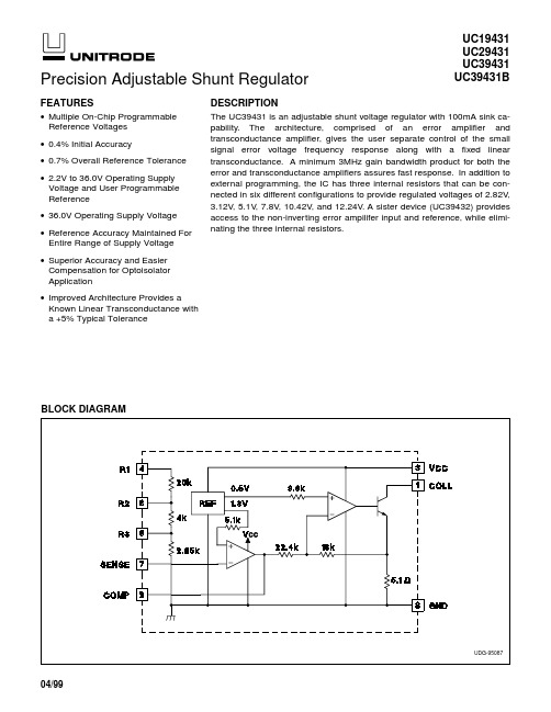
UC29431UC39431UC39431BDESCRIPTIONThe UC39431is an adjustable shunt voltage regulator with 100mA sink ca-pability.The architecture,comprised of an error amplifier and transconductance amplifier,gives the user separate control of the small signal error voltage frequency response along with a fixed linear transconductance.A minimum 3MHz gain bandwidth product for both the error and transconductance amplifiers assures fast response.In addition to external programming,the IC has three internal resistors that can be con-nected in six different configurations to provide regulated voltages of 2.82V ,3.12V ,5.1V ,7.8V ,10.42V ,and 12.24V .A sister device (UC39432)provides access to the non-inverting error ampilifer input and reference,while elimi-nating the three internal resistors.Precision Adjustable Shunt RegulatorFEATURES•Multiple On-Chip Programmable Reference Voltages •0.4% Initial Accuracy•0.7% Overall Reference Tolerance •2.2V to 36.0V Operating Supply Voltage and User Programmable Reference•36.0V Operating Supply Voltage •Reference Accuracy Maintained For Entire Range of Supply Voltage •Superior Accuracy and Easier Compensation for Optoisolator Application•Improved Architecture Provides a Known Linear Transconductance with a +5% Typical ToleranceBLOCK DIAGRAMUC39431BABSOLUTE MAXIMUM RATINGSSupply Voltage: V . . . . . . . . . . . . . . . . . . . . . . . . . . . . .36V Regulated Output: V . . . . . . . . . . . . . . . . . . . . . . . . . . . . . .36V Internal Resistors: R1, R2, R3. . . . . . . . . . . . . . . . . . . . . . .13V E/A Input: SENSE . . . . . . . . . . . . . . . . . . . . . . . . . . . . . . . . .6V E/A Compensation:COMP . . . . . . . . . . . . . . . . . . . . . . . . . .6V Output Sink Current: I. . . . . . . . . . . . . . . . . . . . . . . . . . .140mA Power Dissipation at T A ≤25°C (DIL-8). . . . . . . . . . . . . . . . .1W Derate 8mW/°C for T A > 25°CStorage Temperature Range . . . . . . . . . . . . .–65°C to +150°C Junction Temperature. . . . . . . . . . . . . . . . . . .–55°C to +150°C Lead Temperature (Soldering, 10 sec.). . . . . . . . . . . . .+300°CCurrents are positive into,negative out of the specified termi-nal.Consult Packaging Section of Databook for thermal limita-tions and considerations of packages.ELECTRICAL CHARACTERISTICS:Unless otherwise stated, these specifications apply for T A = –55°C to +125°C andCOLL Output = 2.4V to 36.0V for the UC19431, T A = –25°C to +85°C and COLL Output = 2.3V to 36.0V for the UC29431, and T A = 0°C to +70°C and COLL Output = 2.3V to 36.0V for the UC39431/B,VCC = 15V,I COLL = 10mA, T A =T J .PARAMETERTEST CONDITIONS MIN TYP MAX UNITS Reference Voltage Tolerance T A = 25°C 19431* 1.295 1.3 1.305V 39431B 1.29 1.3 1.31V Reference Temperature Tolerance V COLL = 5.019431* 1.291 1.3 1.309V 39431B 1.2861.3 1.314V Reference Line Regulation Reference Load Regulation VCC =2.2V to 36.0V,V COLL = 5V I COLL = 10mA to 50mA,V COLL = 5V19431*1038mV 39431B 19431*10105738mV mV 39431B1057mV Sense Input Current –0.5–0.2µA Minimum Operating Current VCC = 36.0V,V COLL = 5V 0.500.80mA Collector Current Limit V COLL =VCC = 36.0V, Ref = 1.35V 130145mA Collector Saturation I COLL = 20mA0.7 1.1 1.5V Transconductance (gm)VCC = 2.4V to 36.0V,V COLL = 3V,I COLL = 20mA 19431*–170–140–110mS 39431B –180–140–100mS 5.1V Reference Internal Divider 19431* 5.05 5.1 5.15V 39431B 5 5.1 5.2V 12.24V Reference Internal Divider19431*1212.2412.5V 39431B1212.2412.5V Error Amplifier AVOL 6090dB Error Amplifier GBW(Note 1)3.05MHz Transconductance Amplifier GBW3MHz* Also applies to the UC29431 and UC39431Note:The internal divider can be configured to give six unique references.These references are 2.82V , 3.12V , 5.1V , 7.8V ,10.42V , 12.24V .Note 1:Guaranteed by design.Not 100% tested in production.CONNECTION DIAGRAMUC39431BCOLL:The collector of the output transistor with a maxi-mum voltage of36V.This pin is the output of the transconductance amplifier.The overall open loop volt-age gain of the transconductance amplifier is gm•RL, where gm is designed to be–140mS±30mS and RL rep-resents the output load.COMP:The output of the error amplifier and the input to the transconductance amplifier.This pin is available to compensate the high frequency gain of the error ampli-fier.It is internally voltage limited to approximately 2.0V. GND:The reference and power ground for the device. The power ground of the output transistor is isolated on the chip from the substrate ground used to bias the re-mainder of the device.R1,R2,R3:Connection points to the three internal resis-tors.SENSE:The inverting terminal of the error amplifier used as both the voltage sense input to the error amplifier and its other compensation point.The error amplifier uses the SENSE input to compare against the1.3V on-chip refer-ence.The SENSE pin is also used as the undervoltage lockout (UVLO).It is intended to keep the chip from operating un-til the internal reference is properly biased.The thresh-old is approximately1V.It is important that once the UVLO is released,the error amplifier can drive the transconductance amplifier to stabilize the loop.If a ca-pacitor is connected between the SENSE and COMP pins to create a pole,it will limit the slew rate of the error amplifier.To increase the bandwidth and ensure startup at low load current,it is recommended to create a zero along with the pole as shown in the shunt regulator appli-cation.The error amplifier must slew2.0V to drive the transconductance amplifier initially on.VCC:The power connection for the device.The minimum to maximum operating voltage is2.2V to36.0V.The qui-escent current is typically 0.50mA.PIN DESCRIPTIONS (cont.)UC39431BMagnetic Amplifier Controller ApplicationThe0.4%initial reference makes the UC39431ideal as a programmable shunt regulator.By adding two external resistors,the on-chip1.3V reference can be gained to any voltage between2.2V(2.4V for the UC39431)and 36.0V.The input bias current is typically maintained at 0.2µA for the output voltage range.Since the non-inverting error amplifier input is not available,a5.1k non-inverting input impedance is added to the input of the error amplifier.This allows the user to choose the SENSE pin input impedance to cancel the minimal offset voltage caused by the input bias current.Frequency CompensationThe UC39431shunt regulator is designed with two independant gain stages.The error amplifier provides 90dB of gain with a typical gain bandwidth product of 5MHz.The error amplifier provides sufficient gain in or-der for the sense voltage to be accurately compared to the1.3V on-chip plete control of the fre-quency response of the error amplifier is accomplished with the COMP pin.By putting negative feedback across the error amplifier,either a pole or a pole-zero can be added.The second gain stage is the transconductance(gm)am-plifier.The gm amplifier is designed with a known linear 140mS of transconductance.The voltage gain is conse-quently gm•Ro,where Ro is the output impedance at the collector pin.The frequency response of the transconductance amplifier is controlled with the COLL pin.The gain bandwidth product of the gm amplifier is typically3MHz.A pole or pole-zero can be added to this stage by connecting a capacitor or a series capacitor and resistor between COLL and GND.The compensation of a control loop containing the UC39431is made easier due to the independant com-pensation capability of the error amplifier and gm ampli-fier.As shown in the applications information,a pole-zero is created with a series resistor and capacitor between SENSE and COMP.The pole created is dominant,while the zero is used to increase the bandwidth and cancel the effects of the pole created by the capacitor between the COLL and GND pins.APPLICATION INFORMATIONUC39431BOptocoupler ApplicationThe two amplifier circuit architecture employed in the UC39431is most advantageous for the optocoupler ap-plication.The error amplifier provides a fixed open loop gain that is available to apply flexible loop compensation of either poles or zeroes.A fixed transconductance am-plifier provides a linear current source compared to the typical transistor’s exponential output characteristics.It also eliminates the traditional optocoupler’s CTR varia-tions with power supply and voltage,and the need to suffer the additional voltage drop of a series resistor. Magnetic Amplifier Controller ApplicationThe UC39431makes an excellent controller for magnetic amplifier regulated outputs.Working from either a square wave drive or from a PWM signal controlled by another output,a saturable reactor provides highly efficient con-trol,requiring only a reset current which can be gener-ated from its own output.APPLICATION INFORMATION (cont.)UC39431Bfrequency.UNITRODE CORPORA TION7 CONTINENT AL BLVD.• MERRIMACK, NH 03054Table 1.Resistor divider connection table for shunt applicationsREGULATED VOLTAGE CONNECT R1 TO:CONNECT R2 TO:CONNECT R3 TO:2.82V SENSE (pin 7)COLL(pin 1)SENSE (pin 7)3.12V open COLL(pin 1)SENSE (pin 7)5.1V COLL(pin 1)SENSE (pin 7)open7.8V COLL(pin 1)SENSE (pin 7)GND(pin 8)10.42V COLL(pin 1)SENSE (pin 7)SENSE (pin 7)12.24V COLL(pin 1)open SENSE (pin 7)Note:To obtain the shunt regulated or optocoupler sensed voltage specified in the left column,connect the internal resistors(R1, R2, R3) as indicated.Refer to the shunt regulator application in Fig.1.IMPORTANT NOTICETexas Instruments and its subsidiaries (TI) reserve the right to make changes to their products or to discontinue any product or service without notice, and advise customers to obtain the latest version of relevant information to verify, before placing orders, that information being relied on is current and complete. All products are sold subject to the terms and conditions of sale supplied at the time of order acknowledgement, including those pertaining to warranty, patent infringement, and limitation of liability.TI warrants performance of its semiconductor products to the specifications applicable at the time of sale in accordance with TI’s standard warranty. Testing and other quality control techniques are utilized to the extent TI deems necessary to support this warranty. Specific testing of all parameters of each device is not necessarily performed, except those mandated by government requirements.CERTAIN APPLICATIONS USING SEMICONDUCTOR PRODUCTS MAY INVOLVE POTENTIAL RISKS OF DEATH, PERSONAL INJURY, OR SEVERE PROPERTY OR ENVIRONMENTAL DAMAGE (“CRITICAL APPLICATIONS”). TI SEMICONDUCTOR PRODUCTS ARE NOT DESIGNED, AUTHORIZED, OR WARRANTED TO BE SUITABLE FOR USE IN LIFE-SUPPORT DEVICES OR SYSTEMS OR OTHER CRITICAL APPLICATIONS. INCLUSION OF TI PRODUCTS IN SUCH APPLICATIONS IS UNDERSTOOD TO BE FULLY AT THE CUSTOMER’S RISK.In order to minimize risks associated with the customer’s applications, adequate design and operating safeguards must be provided by the customer to minimize inherent or procedural hazards.TI assumes no liability for applications assistance or customer product design. TI does not warrant or represent that any license, either express or implied, is granted under any patent right, copyright, mask work right, or other intellectual property right of TI covering or relating to any combination, machine, or process in which such semiconductor products or services might be or are used. TI’s publication of information regarding any third party’s products or services does not constitute TI’s approval, warranty or endorsement thereof.Copyright © 1999, Texas Instruments Incorporated。
- 1、下载文档前请自行甄别文档内容的完整性,平台不提供额外的编辑、内容补充、找答案等附加服务。
- 2、"仅部分预览"的文档,不可在线预览部分如存在完整性等问题,可反馈申请退款(可完整预览的文档不适用该条件!)。
- 3、如文档侵犯您的权益,请联系客服反馈,我们会尽快为您处理(人工客服工作时间:9:00-18:30)。
本人使用过程中翻译了本文,水平有限难免有误,欢迎纠正:tyooo@A49313-Phase Brushless DC Motor Pre-Driver三相无刷直流电机前置驱动器4931-DS, Rev. 4下载::/~/media/Files/Datasheets/A4931-Datasheet.ashx下载翻译:2012-11-15▪ ▪ ▪ ▪▪▪ ▪▪本人使用过程中翻译了本文,水平有限难免有误,欢迎纠正: tyooo@A4931 三相无刷直流电机前置驱动器Absolute Maximum RatingsThermal Characteristics*For additional information, refer to the Allegro website.CharacteristicSymbolNotes RatingUnits供电电压Load Supply Voltage V BB38 V 电机输出Motor Phase Output S X t w < 500 ns –3 V 霍尔输入 V Hx DC–0.3 to 7 V 逻辑输入电压范围 V IN–0.3 to 7 V 工作环境温度 T A Range M–20 to 105ºC 最大结温度 T J (max) 150 ºC 储藏温度T stg–40 to 150ºCCharacteristicSymbolTest Conditions*RatingUnits封装内阻,结点到外面(Junction to Ambient )R θJA 4-layer PCB based on JEDEC standard32 ºC/W 封装内阻,结点到焊盘(Junction to Exposed Pad )R θJP2ºC/W本人使用过程中翻译了本文,水平有限难免有误,欢迎纠正: tyooo@A4931 三相无刷直流电机前置驱动器Functional Block DiagramTerminal List0.1 μFNumber 1Name HA+ Description Hall input A 2 HA - Hall input A 3 HB+ Hall input B 4 HB Hall input B 5 HC+ Hall input C 6 HC- Hall input C 7 GND Ground8 HBIAS Hall bias power supply output 9 CP1 Charge pump capacitor terminal 10 CP2 Charge pump capacitor terminal 11 VBB Supply voltage12 VCP Reservoir capacitor terminal 13 SENSE Sense resistor connection 14GLCLow side gate drive CNumber 15 Name GLB Description Low side gate drive B 16 GLA Low side gate drive A 17 GHC High side gate drive C18 SC High side source connection C 19 GHB High side gate drive B20 SB High side source connection B 21 GHA High side gate drive A22 SA High side source connection A 23 FG1 FG 1 speed control output (3 Φ inputs)24 FG2 FG 2 speed control output (ΦA input) 25 CLD Locked rotor detect timing capacitor 26 DIR Logic input – motor direction27 ENABLE Logic input – external PWM control 28BRAKEZLogic input – motor brake (active low)本人使用过程中翻译了本文,水平有限难免有误,欢迎纠正: tyooo@A4931 三相无刷直流电机前置驱动器ELECTRICAL CHARACTERISTICS *Valid at T A= 25°C, V BB= 24 V, unless noted otherwise*Typical data are for initial design estimations only, and assume optimum manufacturing and application conditions. Performance may vary for individualunits, within the specified maximum and minimum limits. For input and output current specifications, negative current is defined as coming out of (sourcing) the specified device pin. Specifications throughout the allowed operating temperature range are guaranteed by design and characterization.本人使用过程中翻译了本文,水平有限难免有误,欢迎纠正:tyooo@ A4931 三相无刷直流电机前置驱动器本人使用过程中翻译了本文,水平有限难免有误,欢迎纠正:tyooo@固定断开时间Fixed Off-Time 理论上A4931的固定断开本人使用过程中翻译了本文,水平有限难免有误,欢迎纠正:tyooo@ A4931 三相无刷直流电机前置驱动器ET Package, 28-Contact QFNFor Reference Only (reference JEDEC MO-220VHHD-1) Dimensions in millimeters Exact caseand lead configuration at supplier discretion within limits shown0.55 +0.20 –0.10Terminal #1 mark area 3.15Exposed thermal pad (reference only, terminal #1 identifier appearance at supplier discretion)Reference land pattern layout (reference IPC7351 QFN50P500X500X100-29V1M); All pads a minimum of 0.20 mm from all adjacentpads; adjust as necessary to meet application process requirements and PCB layout tolerances; when mounting on a multilayer PCB,thermal vias at the exposed thermal pad land can improve thermal dissipation (reference EIA/JEDEC Standard JESD51-5)Coplanarity includes exposed thermal本人使用过程中翻译了本文,水平有限难免有误,欢迎纠正:tyooo@总结1.BREAK:低电平进入刹车状态。
2.ENABLE:低电平时线圈电流持续增加(负载一定则马达加速),直到达到Iୖ୍,Iୖ୍ൌ200mV/Rୗୗ,如果一直为低电则马达速度与Rୗୗ相关;高电平时线圈中的电流开始衰减,如果保持高电平超过3ms(非刹车状态)则进入待机状态;ENABLE上也可加20KHz~30KHz的PWM控制,调节占空比可控制速度,但最大速度受Rୗୗ控制。
3.DIR:控制马达方向。
4.支持三个霍尔信号输入,可为三个霍尔信号提供7.5V/30mV的电源。
5.FG1/FG2:速度反馈,开漏输出,FG1在每个霍尔元件转换时翻转状态,FG2在每个霍尔元件HAx转换时翻转状态。
6.故障关机:温度过高或VBB/VCP欠压时自动关机。
× 20 s/µF,CLD引脚7.锁定检测:FG1没有持续改变或控制时序不正确持续时间超过Tେୈ的情况下将锁定转子,Tେୈ= CLD 接GND则禁止该功能。
8.马达转动时可通过DIR直接切换方向。
9.待机状态与刹车状态的异同:相同点都时马达停转,刹车状态下马达可以自由转动;不同点是待机状态下无霍尔偏压输出(HBIAS引脚无输出),而刹车时有霍尔偏压输出,前者可以达到降低功耗的效果;10.原理图参考前文的应用电路即可,其中有三个参数需要计算:a)CLD引脚电容,参考上面第7点;b)HBIAS到霍尔元件间的电阻Rୌ୍ୗൌሺ7.5VെUୌሻ/Iୌ,Uୌ是工作时霍尔元件上的压降(一般可忽略),Iୌ是霍尔元件正常工作时所需电流,注意是3个霍尔元件;另外要注意HBIAS只能提供7.5V/30mA的电源。
cሻRୗୗ:根据马达最大速度对应的电流参考公式Iୖ୍ൌ200mV/Rୗୗ可求出;注意要保留一定的裕量,使马达在糟糕的情况也能正常工作;。