相位噪声仿真方法
使用ADS仿真相位噪声
Using ADS to simulate Noise FigureADS can be used to design low noise amplifiers much in the same way you have already used it for MAG or MSG designs. Noise circles and available gain circles are the tools that give the most guidance on design tradeoffs. Refer to Chap. 4 and Appendices K and L of Gonzalez for the theory behind these analyses. The ADS files shown below are available from the course web page as a .zap file.Here are 3 cases that you might encounter with device models when analyzing a low noise amplifier.1. The ADS large signal transistor model is used to represent the device. This is the ideal case, but unfortunately, the large signal models sometimes do not produce accurate S parameters. If you use this model, you should check the simulated S parameters with the manufacturer’s data sheet to verify that it provides reasonably accurate results. It should be useful for DC simulations however.2. The ADS S-parameter transistor model is used to represent the device. This is the most accurate case. Of course, no DC simulations will be possible with this model, but it will represent the S parameters and noise parameters accurately. Be sure to select the model that represents the actual bias condition to be used in your analysis.3. No S parameter model is available for the device in the ADS library. In this case, check the manufacturer’s web site and download an S2P file for the device. Place an S2P block from the Data Items menu in your schematic and identify the file name. ADS will look for the file in the ADS project’s data directory. See the appendix at the end of this tutorial for more information on S2P files. In this case, you may have to enter the noise parameters as well using equations on the data display panel.Case 1. Using ADS large signal model library.First you must bias the transistor. Let’s say VCE = 5V and IC = 5 mA. This bias condition might be selected from the plot of noise figure vs. bias condition provided by the manufacturer.Set up a biasing circuit such as the one below. Select a large signal device model from the Analog/RF – RF Transistor/Packaged BJT library. Then perform a DC simulation. To see the results of the DC simulation, you go to the Simulate Menu > Annotate DC solution. Sometimes it is helpful to move component text aside so that the annotation is easier to read. Use F5 to move text.This is the result. We have V CE = 5V and I C = 5.06 mA. (MRF901_DC schematic file) Next, compare the S parameters from the large signal model with those from the small signal measured S parameter model. This model can be found in the Analog/RF S Parameter component library. Simulate over the specified frequency range.(MRF901_sparamtest)From this simulation, we can see that the agreement at our design frequency of 500 MHz is fairly good. S12 is off by about 20%, which will have an effect on the predictions of MSG, but the other parameters fit pretty well at this frequency. Let’s assume this is sufficient. Now we must test for stability.MRF901_large_sig(Display file: stability.dds)We can see that the device is potentially unstable, but if we are careful and can give up some gain, we may be able to find a stable solution and still retain low noise figure. This may give us lower noise figure than if we first make the device unconditionally stable with resistive loading. To evaluate this possibility, we need to look at the available gain and noise figure circles. It is more convenient to calculate the gain and noise circles (Available gain for noise calculations) on the display panel rather than the schematic panel so you can change the noise figure without having to resimulate the circuit.ADS can be used to calculate the noise parameters from the large signal transistor models. You must first enable the S Parameter controller icon for noise simulation. You will generally want to calculate noise parameters at one frequency, so use the Single Point Sweep option on the frequency panel. Also choose Options and set the temperature to 16.85 degrees (standard temperature for noise is 290K).(Display file: circles.dds Use page menu to select gain and noise circles page)The syntax used in the available gain and noise circle equations will be discussed in Section 2. However, you can see in this example, that the MSG is high (19.8 dB), and if we give up 2 dB in gain, a perfect noise source match can be achieved. The noise parameters for the transistor under the given bias condition are shown in the table. These were calculated from the large signal model.Now, you could go back and vary the bias to determine whether you could improve on gain or noise, or you could complete the design by determining matching networks, biasing and wideband stability. Completing the design follows the same procedure described below in Section 2.2. Simulation from S Parameter Model LibraryThe next example illustrates how the noise figure simulations can be carried out using the S Parameter Model Library in ADS. Choosing a different device, we start again by evaluating stability at the design frequency of 500 MHz.NE68139_stabIf the device model includes noise data as this one does in the example above, enable the noise simulation in the S Parameter controller. This will then calculate NFmin, Γopt (called Sopt), and Rn (un-normalized). Also include the maximum gain (MaxGain1) equation (calculates either Maximum Available Gain MAG or Maximum Stable Gain, MSG) and stability circle equations on the schematic panel. You must first determine stability before proceeding with the noise analysis. Since this is a low noise design, wewill try first for a solution that does not require resistive stabilization which would degrade the noise figure.(Display file: stability.dds)We can see that the device is potentially unstable, but if we are careful and can give up some gain, we may be able to find a stable solution and still retain low noise figure. To evaluate this, we need to look at the available gain and noise figure circles. The noise parameters needed for noise figure calculation are not included in the S Parameter model library, so they must be added to the display panel. It is more convenient to calculate the gain and noise circles (Available gain for noise calculations) on the display panel rather than the schematic panel so you can change the noise figure without having to resimulate the circuit.The syntax for calculating available gain circles (ga_circle equation) is the same as that for power gain circles. It is usually convenient to plot the gains relative to the MaxGain1 value. The Gav circles must be plotted on the source plane. They assume that the load is conjugately matched to the output for all ΓS values.The noise circle parameters (for the ns_circle equation) are defined as:ns_circle(nf, NFmin, gamma_opt, rn, 51)nf = noise figure of the device represented by ΓS values that fall on the circle.NFmin = minimum possible noise figure of device at this bias and frequencyGamma_opt = Γopt = the optimum input match for best noise figurern = the noise resistance parameter (normalized to 50 ohms)51 = number of points plotted on the circleIf the transistor model does not include noise data (not all of them do), you must enter the NFmin, gamma_opt, and rn from the transistor data sheet manually using equations (Eqn) in order to calculate noise circles.(Display file: circles.dds Use page menu to select gain and noise circles page)In this example, you can see that MSG is quite high: 24 dB at 500 MHz. If we mismatch the input such that we give up 3 dB of available gain (brown gain circle), we can come quite close to the minimum noise figure of the device (1.15 dB). In fact, a ΓS = 0 (very simple match!) could give a NF somewhere between 1.15 and 1.5 dB.Once you have decided on the ΓS value, place the marker there on the display. You need to design matching networks for the source and load. Calculate the corresponding ΓL with the usual equation as shown below. Using the circles data display file, use the page menu to select the Gamma L page. Check the load stability circle to make sure ΓL doesnot fall in an unstable region, and design the output matching network to provide ΓL.(Display file: circles.dds Use page menu to select gamma L page)Then, design the matching networks, provide for bias insertion, and simulate the amplifier over a range of frequencies to verify stability out of band just as you did in the Stability and Gain tutorial.Appendix 1: Representing devices as an S2P fileIn the case of the NE34018, the ADS component library does not contain a set of S parameters for the device. Instead, we can use an S2P file provided by NEC. The file for our device was measured at the VDS = 2V; ID = 5 mA bias point. An S2P file is simply a tab delimited ASCII text file containing S parameters measured on a 2 port device. The format is:Frequency S11 S21 S12 S22In GHz mag ang mag ang mag ang mag angPlace an S2P block from the Data Items menu and identify the file name. ADS will look for the file in the ADS project’s data directory.。
pss+phase noise仿真方法
pss+phase noise仿真方法随着现代电子设备的广泛应用,相位噪声问题越来越受到人们的关注。
相位噪声是信号在传输过程中由于各种因素的影响而产生的随机起伏变化,它会影响设备的性能和稳定性。
为了更好地理解和控制相位噪声,本文介绍了一种基于PSS (Phase-SensitiveSignal)的相位噪声仿真方法。
一、引言相位噪声仿真是一种用于评估电子设备在特定频率下的相位噪声性能的方法。
这种方法可以帮助工程师在设计过程中预测设备的性能,从而优化电路设计和参数配置。
传统的相位噪声仿真方法通常采用数字滤波器或傅里叶变换等算法,但这些方法存在一定的局限性。
为了解决这些问题,本文提出了一种基于PSS的相位噪声仿真方法,该方法具有更高的精度和灵活性。
二、PSS理论基础PSS是一种基于相位敏感的信号处理方法,它能够准确地检测和处理信号中的相位噪声。
在PSS方法中,信号被分解为多个频率分量,每个分量都被单独处理。
这种方法能够更准确地模拟信号传输过程中的各种因素,如调制、滤波等,从而更准确地评估相位噪声性能。
三、仿真方法实现1.建立仿真模型:首先,根据设备的设计和参数配置建立仿真模型。
模型中包括输入信号、放大器、滤波器、混频器等组件。
2.输入信号生成:根据实际应用场景,生成输入信号。
输入信号可以是连续波信号或调制信号,并考虑信号的调制方式和频率。
3.PSS处理:使用PSS方法对输入信号进行处理,得到各个频率分量的相位噪声数据。
4.数据分析:对得到的相位噪声数据进行统计分析,评估设备的相位噪声性能。
5.结果输出:将结果以图表或数值形式输出,供工程师参考和优化设计。
四、仿真结果分析通过仿真实验,我们可以得到设备的相位噪声性能数据。
根据这些数据,我们可以分析设备的性能特点,如噪声水平、频率稳定性等。
同时,我们还可以比较不同设计方案的性能差异,为优化设计提供依据。
通过将仿真结果与实际测试结果进行对比,我们可以验证仿真方法的准确性和可靠性。
信道建模 相位噪声
相位噪声,一般指振荡器产生的信号的相位随机波动的现象。
在通信系统中,信道建模是建立信道数学模型的过程,用于描述信号在通过信道时的传输特性。
而信道的噪声可以看作加性干扰,它独立于信号始终存在,无论有无信号输入,噪声都始终存在。
具体来说,信道的噪声在频谱(频域)上呈均匀分布(即白噪声),而在幅度上(时域)则表现为高斯分布。
同时,接收信号功率Pr和噪声功率谱密度(PSD)的关系决定了信噪比(SNR)。
对于每符号有 k = log_2 (M) 位的未编码 M-ary 信号方案,调制符号的信号能量由特定公式给出,从而可以计算出每符号的信噪比。
在设计过程中,为了对相位噪声的影响进行建模,首先会产生零均值高斯白噪声,然后使噪声通过一个无限冲激响应(IIR)滤波器,再把滤波后的噪声添加到输入信号的角度分量中。
这样做的目的是为了更准确地模拟和预测相位噪声对信号传输的影响。
压控振荡器相位噪声的一种建模研究方法
2O4 , O2O 嘶
; 2 Sho f col t nc S a g J o n n esy S a g 204 , h ̄ ) .c ol re cr i, hn  ̄ ' t gU i ri , hn  ̄ 020 C iq o Mi e o m o v t
Ab ta t L — CO i ids e sbefrta s ev r n w rls o sr c : C V S n ip na l o n c iesi i e sc mmu ia o .T e p r yo p cr m r e nc f n i h u i fs et t u
p r s i a a i n e a e s u d o e e i e aey t u i lt n . I i w y,t e i a to a a i c c p ct c s C b h ta p n d l r tl o r n s t a n n b mu a o s n t s a i h h mp c f d f r n os o r e n i e n aa i c c p ctn e n t e p a en i a eo s r e .Us gt i i e e t i s u c sa d df r t r s i a a i c so h s o s C l b b e v d n e e p t a h e l i s n h
2 1 年第1 00 期
中图分类号 :N 5 T 72 文献标识码 : A 文章编 号 :09— 52 2 1 )7— 06— 5 10 2 5 (0 0 0 0 3 0
压 控振 荡 器 相位 噪 声 的 一种 建模 研 究 方 法
胡晓莉 李章全 李 萍 , ,
(.上海交通大学 电信学院电子工程 系 , 1 上海 204 ; .上海交通大学微 电子学院 , 020 2 上海 204 ) 020
LC低相位噪声压控振荡器设计与仿真

() 6
由式 () 见 , 出 有 三 个 频 率 分 量 , c ,, 6可 输 即 c c , c o o一 和c £ £ 。 c ±c , , 在 £ £ 相对 于载 波功 率 的噪 o+c , , o 处 声等 于 ( c ) / 。 际 中 ,, 在 无 数 可 能 Kv o 4实 c c 存 的取值 , 以它 的干 扰 频谱 是 很 宽 的。 种 噪声 的 所 此 影响 随 c 的 降 低 而 更 突 出 。 为 在 控 制 路 径 中 c , 因
频率 1 1 H —13 H 的低相位噪声 V O进行设计和仿真。 .G z .G z C 关键词 压控振荡器 ; 相位 噪声 ; 设计
T 3 19 P 9 . 中图 分 类 号
L L w h s i l g - o to ld Os i a o sg n i l t n C o P a e Nos Vo t e— c n r l cl t r De i n a d S mu a i e a e l o
o h s os fp a e n i eme h ns n cai mso
meh d o ein n C v l g to fd sg igL ot e—c nrl d ocl t hc su e nRF C p p lr ,te rs n e a o t l s i ao oe l rw ihi sdi I o ua l h n pe e tsa y
中。相位噪声是 V O的一项关键参 数, C 在通信 系 统的收发信机 中, 相位噪声将引起相邻信道干扰、 灵 敏度及 动态 范 围 恶化 、 制 解 调 错 误 等 影 响 , 调 所
以设计 低 相位 噪声 压控 振 荡 器 对 提 高 通 信 系统 的 性 能是 十分重要 的 。
matlab 相位噪声
MATLAB相位噪声引言MATLAB是一种功能强大的数值计算环境和编程语言,它的广泛应用让我们能够进行各种科学和工程领域的计算和分析。
相位噪声是MATLAB中一个重要的研究主题,本文将对MATLAB相位噪声进行全面、详细、完整且深入的探讨。
什么是相位噪声在MATLAB中,相位噪声是指信号的相位部分存在不稳定性或随机性的情况。
相位噪声可以产生于各种信号处理系统或通信系统中,它会导致信号的频率不确定性或时序不良,从而影响到系统的性能和准确性。
相位噪声的特征及影响相位噪声通常具有以下特征:1.高度随机性:相位噪声是一种随机过程,其发生规律难以预测,具有很高的不确定性。
2.频谱分布广:相位噪声在不同频率范围内具有不同的功率分布,通常呈现为低频部分较强的特点。
3.对系统性能的影响:相位噪声会引起系统的频偏、抖动等问题,从而降低系统的性能和准确性。
相位噪声在一些特定的应用领域中会带来严重的影响,比如通信系统、雷达系统、时钟同步系统等。
在这些系统中,相位噪声对信号传输的准确性和可靠性有着重要的影响。
相位噪声的产生机制和建模方法相位噪声的产生机制通常与信号的生成和传输过程有关。
在MATLAB中,可以采用不同的建模方法来模拟相位噪声,其中比较常用的方法包括:1.随机游走模型:基于随机游走的模型可以较好地描述相位噪声的特性,其基本思想是通过随机过程模拟相位的变化。
2.频率鉴别器:通过频率鉴别器可以实现相位噪声的建模,它是一种在频域上对信号进行频率测量的滤波器。
3.相位估计方法:通过相位估计的方法可以对相位噪声进行建模和矫正,其中包括基于滤波器的相位估计和估计误差等。
这些建模方法可以根据不同的应用场景选择合适的模型,并通过MATLAB进行相应的实现和分析。
相位噪声的实际应用相位噪声在许多科学和工程领域中都有着广泛的应用,其中几个典型的应用领域包括:1.音频信号处理:相位噪声对音频信号的音质有着重要的影响,因此在音频信号处理中通常需要对相位噪声进行建模和补偿。
相位噪声仿真方法
H z
f 噪声
图 2.5 f
噪声的生成原理示意图
图 2.5 中的成形滤波器一般采用低通滤波器实现,调整滤波器参数,利用低通 滤波器的低通特性和过渡带形状改变高斯白噪声的噪声功率谱分布,以产生不同 功率谱特性的噪声分量。如采用 FIR 滤波器实现,其系统函数[109]为:
3. 基于幂律谱模型的相位噪声仿真步骤
式(2.61)
由上述讨论的内容可总结出基于幂律谱模型的相位噪声仿真实现过程。若需 要 仿 真 生 成 长 度 为 N 的 相 位 噪 声 仿 真 数 据 , 采 样 率 为 fs , 噪 声 系 数 为
h
生成闪烁噪声的 FIR 滤波器阶数为 k , 则采样间隔 1/ f s , 2, 1,0,1, 2 ,
该模型即为相位噪声的幂律谱模型,其中 0,1, 2,3, 4 ,分别对应相位噪声中 的相位白噪声、相位闪烁噪声、频率白噪声、频率闪烁噪声、随机游走频率相位 噪声。 2.2.2 基于幂律谱模型的相位噪声仿真方法
根据式(2.49)和式(2.56)表示的相位噪声幂律模型, 要产生振荡器信号的相位噪 声数据序列,可以分别产生幂律模型中五种不同的噪声分量,将其合成为所需的 相位噪声数据序列。上述相位噪声数据仿真方法主要需要实现两个方面的问题: 五种幂律谱噪声数据的生成;将产生的五种噪声按指定的噪声分量系数合成为能 真实反映指定噪声分量系数的振荡器相位噪声数据。以下分别研究这两个问题。 1. 五种幂律谱噪声数据的生成 根据式(2.56)给出的相位噪声模型,主要研究相位白噪声、相位闪烁噪声、频 率白噪声、频率闪烁噪声、随机游走频率相位噪声五种噪声数据的生成。根据其 定义和频谱特征, 五种噪声的噪声功率在频域和频率的关系分别为 f 0 、f 1 、f 2 、
锁相频率合成器相位噪声的精确估计与仿真(优选)word资料

锁相频率合成器相位噪声的精确估计与仿真(优选)word资料2006 年 10 月 JOURNAL OF CIRCUITS AND SYSTEMS October , 2006 文章编号:1007-0249 (2006 05-0128-04锁相频率合成器相位噪声的精确估计与仿真*邓贤进1,2, 李家胤2, 张健1(1. 中国工程物理研究院电子工程研究所,四川绵阳 621900;2. 电子科技大学,四川成都 610054摘要:实现对相位噪声的精确估计必须考虑环路中电阻噪声的影响。
从建立并分析电阻噪声模型出发,设计了两种都能满足基本技术指标的环路滤波器。
用仿真手段对这两种不同的环路滤波器进行了仿真,清楚地表明了电阻对相位噪声的影响。
最后的实验结果证明了这种估计方法的精确性。
关键词:锁相环;频率源;相位噪声;仿真中图分类号:TN974 文献标识码:A1 引言频率源的相位噪声是一项非常重要的性能指标,它对电子设备和电子系统的性能影响很大,从频域看它分布在载波信号两旁按幂律谱分布。
用这种信号不论做发射激励信号,还是接收机本振信号以及各种频率基准时,这些相位噪声将在解调过程中都会和信号一样出现在解调终端,引起基带信噪比下降。
在通信系统中使话路信噪比下降,误码率增加;在雷达系统中影响目标的分辨能力,即改善因子。
接收机本振的相位噪声,当遇到强干扰信号时,会产生“倒混频”使接收机有效噪声系数增加。
所以随着电子技术的发展,对频率源的相位噪声要求越来越严格,因为低相位噪声,在物理、天文、无线电通信、雷达、航空、航天以及精密计量、仪器、仪表等各种领域里都受到重视。
因此,针对不同用途的频率源的设计,需要对预设计的频率源相噪指标进行准确的估计,以达到有的方矢,缩短设计周期。
影响相噪指标的因素很多,通常,设计者会根据主要器件本身的性能参数和环路参数来粗略估计频率源的相噪指标,但往往忽略了环路滤波器中电阻和放大器本身的噪声所带来的相噪指标的恶化。
pss+phase noise仿真方法
pss+phase noise仿真方法摘要:1.PSD和相位噪声的基本概念2.PSD+相位噪声仿真方法的重要性3.详细步骤:仿真原理、仿真工具、参数设置和结果分析4.应用场景和优势5.总结与展望正文:随着现代通信技术的发展,对信号质量的要求越来越高,PSD(功率谱密度)和相位噪声成为衡量信号质量的重要参数。
PSD描述了信号功率在频率上的分布,而相位噪声则反映了信号相位的起伏。
为了更好地研究和优化信号质量,PSD+相位噪声仿真方法应运而生。
PSD+相位噪声仿真方法的重要性体现在以下几点:首先,通过仿真可以更直观地了解信号的功率和相位分布,为信号设计提供参考;其次,仿真有助于分析不同噪声源对信号质量的影响,从而采取相应的抑制措施;最后,仿真结果可以指导实际系统的优化和调试。
接下来,我们将详细介绍PSD+相位噪声的仿真方法。
1.仿真原理:首先,根据信号的PSD和相位噪声模型,建立信号的数学表达式。
然后,利用傅里叶变换等算法将时域信号转换为频域信号,从而分析信号的PSD和相位噪声特性。
2.仿真工具:市面上有很多专业的仿真软件,如MATLAB、Python等,可以实现PSD和相位噪声的仿真。
此外,一些通信系统仿真软件,如SystemView、NI LabVIEW等,也可以完成相关仿真任务。
3.参数设置:在进行仿真时,需要设置信号的参数,如频率、幅度、噪声模型等。
同时,还需要设定仿真时间、采样率等参数。
根据实际需求,可以调整这些参数以获得更为准确的仿真结果。
4.结果分析:仿真完成后,可以通过观察频谱图、PSD曲线和相位噪声特性等手段,分析信号质量。
此外,还可以通过计算相关指标,如信噪比、相位噪声指数等,对信号进行量化评估。
PSD+相位噪声仿真方法在通信、雷达、超声波等领域具有广泛的应用。
通过仿真,可以有效提高信号质量,降低系统噪声,从而提升系统的性能。
总之,PSD+相位噪声仿真方法在信号设计和优化中发挥着重要作用。
(sweep)及Pnoise的仿真
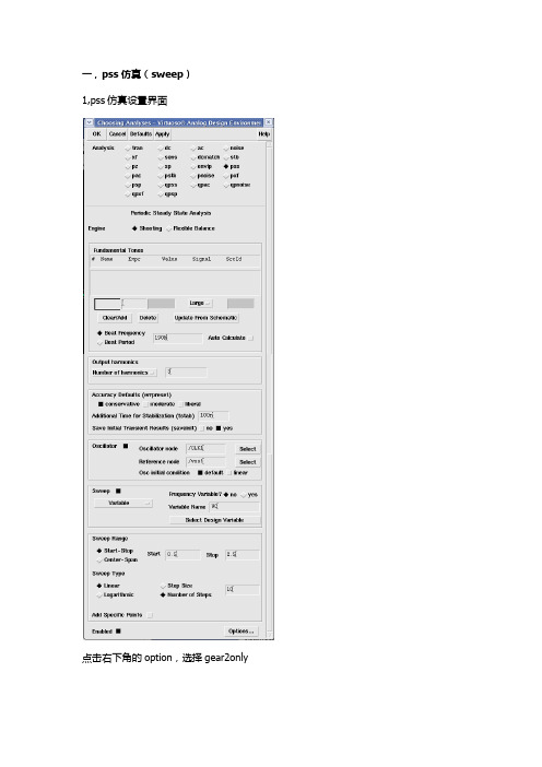
一,pss仿真(sweep)
1,pss仿真设置界面
点击右下角的option,选择gear2only
在将控制电压VC设置成变量的时候注意设置方法如下Setup—Stimuli…
然后添加变量
Beat Frequency是振荡器的近似振荡频率,可以通过Tran仿真得到。
2,查看pss的sweep仿真结果
Result—Direct Plot—Main From
然后出现下面的窗口,按照窗口中的选择,点击Beat Frequency为1的那行,然后点下侧的Plot就会出现振荡频率随控制电压的调谐波形。
频率调谐波形
二,Pnoise仿真
1,在进行pnoise仿真时要将pss仿真的sweep关掉,只仿真控制电压的一个点的相位噪声,这样仿真速度就要快很多。
另外,相噪的仿真是和pss仿真一起进行的。
2,相噪仿真设置
3,相噪仿真后的波形观察Result—Direct Plot—Main From
点击Plot就可以出现波形。
振荡器相位噪声的仿真_物联网:ADS射频电路仿真与实例详解_[共3页]
![振荡器相位噪声的仿真_物联网:ADS射频电路仿真与实例详解_[共3页]](https://img.taocdn.com/s3/m/37df99d876c66137ef061906.png)
第
19章 射频振荡器的仿真501
║
图19.37 瞬态仿真控制器图19.38 压控振荡器的瞬态输出曲线
用来显示输出信号频谱的方程如图19.39所示。
(7)在数据显示视窗显示仿真的频谱输出,步骤如下。
在显示方式面板中选择矩形图显示方式,插入到数据显示视窗中。
在【Plot Traces & Attributes】窗口中选择Equations。
在Equations项目下,选择Spectrum。
在Spectrum
矩形图中插入一个标记,标记插入到Spectrum幅度最大处。
频谱输出Spectrum的曲线如图
19.40所示,单击工具栏中的按钮,保存数据。
图19.39 用来显示输出信号频谱的方程图19.40 压控振荡器的频谱输出曲线(8)由图19.38和图19.40可以看出,振荡器已经很稳定地振荡起来了。
由图19.38可以看出,振荡器的振荡幅度为585mV。
由图19.40可以看出,振荡器的振荡频率为1.804GHz。
19.3.5 振荡器相位噪声的仿真
对振荡器原理图进行谐波平衡仿真,可以分析振荡器的相位噪声。
分析振荡器相位噪声的步骤如下。
(1)将原理图VCO-3另存为原理图VCO-4。
(2)删除原理图VCO-4中的瞬态仿真控制器。
(3)在谐波平衡仿真【Simulation-HB】元器件面板上,选择谐波平衡仿真控制器HB插入到原理图中,对谐波平衡仿真控制器HB设置如下。
Freq[1] =1.8GHz,表示谐波平衡仿真的基准频率为1.8GHz。
Order[1] =9,表示谐波平衡仿真时基波频率的最大谐波次数为9。
相位噪声基础及测试原理和方法

相位噪声基础及测试原理和方法相位噪声是指在波形信号中,信号的相位随时间的变化引起的误差或扰动。
相位噪声对于许多通信系统和测量系统都是一个非常重要的参数,因为它会影响信号的稳定性和准确性。
本文将介绍相位噪声的基础知识、测试原理和方法。
一、相位噪声的基础知识相位噪声是指信号在频率上的扩展,它的频谱密度随频率的增加而增大。
相位噪声可以分为两种类型:低频相位噪声和高频相位噪声。
低频相位噪声是指在较低的频率范围内信号相位的波动,而高频相位噪声则是指在较高的频率范围内信号相位的波动。
相位噪声可以由多种因素引起,包括信号源的本身性能、环境噪声和非线性失真等。
其中,信号源的相位噪声对于通信系统的性能有较大的影响,因为它会引起信号的抖动和时钟误差。
为了准确测量信号源的相位噪声,我们需要使用相位噪声测试仪。
常用的相位噪声测试仪有频率鉴相器、相位抖动测试仪和数字频率合成器等。
1.频率鉴相器法:频率鉴相器法是一种直接测量相位噪声的方法。
它的基本原理是将待测信号与参考信号进行鉴相,然后通过解调信号来获取相位噪声的频谱密度。
频率鉴相器法的优点是能够直接测量相位噪声,但缺点是需要提供一个好的参考信号。
2.相位抖动测试仪法:相位抖动测试仪法是一种间接测量相位噪声的方法。
它的基本原理是通过测量信号的抖动来推导相位噪声的频谱密度。
相位抖动测试仪法的优点是测量简单,不需要提供参考信号,但缺点是测量精度相对较低。
3.数字频率合成器法:数字频率合成器法是一种综合利用数字信号处理技术来测量相位噪声的方法。
它的基本原理是通过数字信号处理算法来估计信号的相位噪声频谱密度。
数字频率合成器法的优点是测量精度高,但缺点是需要复杂的数字信号处理算法。
除了上述方法,还可以使用功率谱仪和频谱分析仪等设备来测量相位噪声。
三、相位噪声测试的注意事项在进行相位噪声测试时,需要注意以下几点:1.选择合适的测量设备:不同的相位噪声测试原理和方法适用于不同的应用场景,需要根据具体情况选择合适的测量设备。
脉冲调制信号的相位噪声恶化仿真
中 图分 类号 : T N 6 2 2 文献标志码 : A 文章 编 号 : 1 0 0 4 — 7 8 5 9 ( 2 0 1 5 ) 0 8 — 0 0 4 6 — 0 3
励 信 号 的关 键 指 标 之 一 , 是 衡 量 信 号 质 量 的 关 键 依 据 … 。 因此 , 在各种频率源系统设计 中, 该 指 标 作 为
重要 指标 被考 核 , 并 且 该 指标 的测 量 大 多是 基 于 连 续
后利 用 S y s t e m V u e软件搭 建 了仿 真模 型 对脉 冲调 制后 相 位噪声 恶化 程度 进行 量化 仿真分 析 。
Ab s t r a c t : I n o r d e r t o a n a l y s e t h e p h a s e n o i s e d e t e r i o r a t i o n d e g r e e o f c o n t i n u o u s wa v e a f t e r p u l s e mo d u l a t i o n,s i mu l a t i o n mo d e l f o r p u l s e mo d u l a t i o n u s i n g S y s t e mV u e s o f t wa r e i s b u i l t i n t h i s p a p e r .T h r o u g h t h e s i mu l a t i o n r e s u l t s :t h e p h a s e n o i s e a f t e r p u l s e mo d u —
相位噪声基础及测试原理和方法
摘要^相位噪声指标对于当前的射频微波系统、移动通信系统、雷达系统等电子系统影响非常明显,将直接影响系统指标的优劣。
该项指标对于系统的研发、设计均具有指导意义。
相位噪声指标的测试手段很多,如何能够精准的测量该指标是射频微波领域的一项重要任务。
随着当前接收机相位噪声指标越来越高,相应的测试技术和测试手段也有了很大的进步。
同时,与相位噪声测试相关的其他测试需求也越来越多,如何准确的进行这些指标的测试也愈发重要。
1、引言随着电子技术的发展,器件的噪声系数越来越低,放大器的动态范圉也越来越大,增益也大有提高,使得电路系统的灵敬度和选择性以及线性度等主要技术指标都得到较好的解决。
同时,随着技术的不断提高,对电路系统乂提岀了更高的要求,这就要求电路系统必须具有较低的相位噪声,在现代技术中,相位噪声已成为限制电路系统的主要因素。
低相位噪声对于提高电路系统性能起到重要作用。
相位噪声好坏对通讯系统有很大影响,尤其现代通讯系统中状态很多,频道乂很密集,并且不断的变换,所以对相位噪声的要求也愈来愈高。
如果本振信号的相位噪声较差,会增加通信中的误码率,影响载频跟踪精度。
相位噪声不好,不仅增加误码率、影响载频跟踪精度,还影响通信接收机信道内、外性能测量,相位噪声对邻近频道选择性有影响。
如果要求接收机选择性越高,则相位噪声就必须更好,要求接收机灵敬度越高,相位噪声也必须更好。
总之,对于现代通信的各种接收机,相位噪声指标尤为重要,对于该指标的精准测试要求也越来越高,相应的技术手段要求也越来越高。
2、相位噪声基础2.K什么是相位噪声相位噪声是振荡器在短时间内频率稳定度的度量参数。
它来源于振荡器输出信号由噪声引起的相位、频率的变化。
频率稳定度分为两个方面:长期稳定度和短期稳定度,其中,短期稳定度在时域内用艾伦方差来表示,在频域内用相位噪声来表示。
2.2.相位噪声的定义以载波的幅度为参考,在偏移一定的频率下的单边带相对噪声功率。
这个数值是指在1Hz的带宽下的相对噪声电平,其单位为dBc/Hzo该定义最早是基于频谱仪法测试相位噪声,不区分调幅噪声和调相噪声。
iq 相位噪声测试方法
iq 相位噪声测试方法IQ相位噪声是衡量通信系统中信号质量的重要参数之一。
准确的相位噪声测试对于优化系统性能、保障通信质量具有重要意义。
本文将详细介绍IQ相位噪声的测试方法,帮助读者掌握相关技术要领。
一、IQ相位噪声概述IQ相位噪声是指IQ调制信号在传输过程中,由于各种原因导致的相位波动。
这种波动会影响信号的传输质量,降低通信系统的性能。
为了评估相位噪声对通信系统的影响,需要对其进行准确的测试。
二、IQ相位噪声测试方法1.矢量信号分析仪法矢量信号分析仪是进行IQ相位噪声测试的常用设备。
其主要原理是通过采集待测信号的IQ数据,分析其相位波动情况,从而得到相位噪声的参数。
测试步骤如下:(1)连接矢量信号分析仪与待测设备,确保信号传输路径无误。
(2)设置矢量信号分析仪的参数,如采样率、带宽等,使其适应待测信号。
(3)对待测信号进行采样,获取IQ数据。
(4)使用矢量信号分析仪内置的相位噪声分析功能,对待测信号的相位波动进行计算。
(5)根据计算结果,得到相位噪声的参数,如均方根值(RMS)等。
2.数字信号处理法数字信号处理(DSP)技术也可以用于IQ相位噪声测试。
这种方法通过对待测信号的数字样本进行处理,提取相位信息,从而计算相位噪声。
测试步骤如下:(1)对待测信号进行采样,获取数字样本。
(2)利用数字信号处理算法,如快速傅里叶变换(FFT),对数字样本进行处理,提取相位信息。
(3)分析相位信息,计算相位噪声参数。
(4)根据计算结果,评估相位噪声对通信系统的影响。
三、注意事项1.测试过程中,应确保信号传输路径的稳定性和一致性,避免外部干扰。
2.选择合适的测试设备和方法,以适应不同类型的待测信号。
3.测试前,对设备进行校准,确保测试结果的准确性。
4.在实际应用中,可以结合多种测试方法,相互验证,提高测试结果的可靠性。
总结:IQ相位噪声测试是评估通信系统性能的关键技术之一。
掌握合适的测试方法,可以有效提高通信系统的性能,保障通信质量。
相位噪声&抖动仿真方法VCO Design Using SpectreRF
VCO Design Using SpectreRF
________________________________________________________________________
Contents
Voltage Controlled Oscillator Design Measurements ........................................................ 3 Purpose............................................................................................................................ 3 Audience ......................................................................................................................... 3 Overview......................................................................................................................... 3 Introduction to VCOs.......................................................................................................... 3 The Design Example: oscHartley ....................................................................................... 4 Example Measurements Using SpectreRF.......................................................................... 5 Lab1: Output Frequency, Output Power, Phase Noise and Jitter ................................... 6 Measurement (Pnoise with shooting or Flexible Balance engine).................................. 6 Lab2: Frequency Pushing (Swept PSS) ........................................................................ 31 Lab3: Tuning Sensitivity and Linearity (Swept PSS)................................................... 36 Lab4: Power Dissipation (PSS) ................................................................................... 43 Lab5: Frequency Pulling (Swept PSS) ........................................................................ 48 Conclusion ........................................................................................................................ 62 Reference .......................................................................................................................... 62
利用仿真工具分析相位噪声对接收机的影响
利用仿真工具分析相位噪声对接收机的影响作者:梁大恒来源:《电子技术与软件工程》2013年第22期摘要在超外差接收机中,本振的相位噪声会对接收机抗干扰能力有影响。
本文讲述如何利用仿真工具精确分析相位噪声对接收机的影响,可以依据本方法的分析结果确定接收机本振的噪声特性要求。
【关键词】相位噪声接收机抗干扰在超外差接收机中,需要有本振信号在接收机中将射频信号变成中频信号。
对于一个应输出频率为f0的信号源,在理想状态下,其输出的信号能量应该都集中在f0这个频点上。
但实际情况是,频率为f0的信号,其每个周期1/f0,时域上是很难完全一致的,于是就出现了抖动,这些抖动在频域上表现出来就是f0的附近也有信号能量分布,这些能量就是相位噪声。
相位噪声的单位形式是偏移载波中心的某处的1Hz带宽的频谱能量与载波功率的比,如-125dBc/Hz@1MHz。
相位噪声对超外差接收机的双信号选择性性能有影响,双信号选择性是指接收机在有接收信号存在时,对临近信道干扰信号的抑制能力。
对于超短波设备,一般会考虑在距离工作频率1个信道、10个信道等位置施加干扰来测试设备的双信号选择性。
对于信道带宽50kHz的设备,一般会在距离工作频率50kHz、500KHz、1MHz、5MHz等位置施加干扰。
本文将利用NI公司提供的仿真工具AWRDE搭建接收机仿真模型,并结合某些设备的具体指标来分析本振相位噪声对接收机双信号选择性的影响。
本文的设备工作频率是200MHz,工作带宽是50kHz,干扰测试频率是50kHz、200KHz、1MHz。
设备的设计任务书上对双信号选择性的要求为50kHz处优于40dB、200kHz处优于80dB、1MHz处优于100dB。
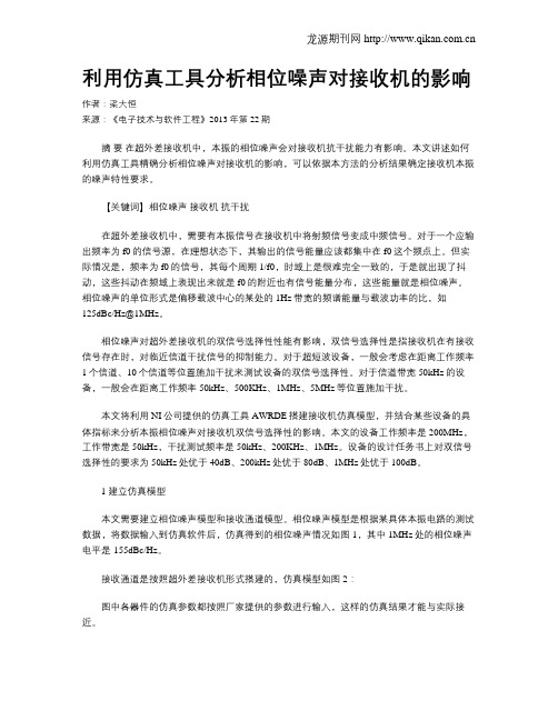
1 建立仿真模型本文需要建立相位噪声模型和接收通道模型。
相位噪声模型是根据某具体本振电路的测试数据,将数据输入到仿真软件后,仿真得到的相位噪声情况如图1,其中 1MHz处的相位噪声电平是-155dBc/Hz。
- 1、下载文档前请自行甄别文档内容的完整性,平台不提供额外的编辑、内容补充、找答案等附加服务。
- 2、"仅部分预览"的文档,不可在线预览部分如存在完整性等问题,可反馈申请退款(可完整预览的文档不适用该条件!)。
- 3、如文档侵犯您的权益,请联系客服反馈,我们会尽快为您处理(人工客服工作时间:9:00-18:30)。
1的分量,表示相位噪声相对频率波动谱密度 S y ( f ) 中与频率 f 1 成比例
关系的分量,称为频率闪烁噪声,其时域过程为非平稳随机过程,引起相位的长 周期随机漂移,描述信号的长期稳定性能。
2 的分量,表示相位噪声相对频率波动谱密度 S y ( f ) 中与频率 f 2 成比例
关系的分量,称为频率随机游走噪声,其时域过程为非平稳随机过程,引起相位
22
第二章 相位噪声理论与仿真方法
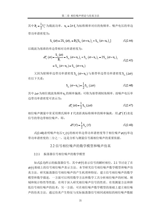
的长周期连续漂移,描述信号的长期稳定性能。 振荡器信号的相位噪声是这五种幂律噪声项的部分或全部,这要视振荡器的 具体情况而定。在不同的取样时间,主导噪声不同,也就是说,在某一个频率区 间,有一种噪声起主导作用。 由于:
L (f) 1 S ( f ) 2 n
f 表是
式(2.48)
式(2.48)表明噪声电压 vn t 的相对单边带功率谱密度等于相位噪声 t 单边 带功率谱密度的二分之一,这是分析与测量信号源相位噪声的重要依据。
2.2 信号相位噪声的数学模型和噪声仿真
2.2.1 振荡器信号相位噪声的数学模型
如式(2.5)所示的振荡器信号,其中 t 表示信号的瞬时相位,2.1 节讨论了在
t 基础上的信号相位噪声表示方法。本节研究信号相位噪声数学模型和噪声仿
真方法。研究振荡器信号相位噪声的产生机理和特征,建立信号相位噪声的数学 模型和数学描述,一方面可以利用数学方法和数学工具分析相位噪声的时域、频 域和统计特性等性能,有利于深入研究相位噪声信号的性质、有效测量方法和降 低信号相位噪声的技术;另一方面,可在相位噪声数学模型的基础上建立相位噪 声的仿真方法,通过仿真产生特征与实际振荡器信号相同或相似的相位噪声数据
L
f
1 S f 2
由式(2.52)和式(2.55)可知,信号的单边带功率谱密度 L
1 2 4 1 0 h2 f L f S f 2 0 2 0
根据相位噪声的频域特征,这五个频谱分量可以表示为关于频率的幂律函数[67],
h2 f 2 h1 f 1 h0 h1 f 1 h2 f 2 当0 f f h Sy ( f ) 0 当f f h
即:
式(2.51)
2 h f S y f 2 0
y t
可得:
d t t 2 0 dt 2 0 1
2Hale Waihona Puke 式(2.53)1 S y ( f ) f 2 S f v0
式(2.54)
其中 S f 为信号的相位波动功率谱密度,信号的单边带功率谱密度 L
f 为:
式(2.55)
第二章 相位噪声理论与仿真方法
1 其中 PS V02 为载波功率, u0 2 f0 为标称频率对应的角频率。噪声电压的单边 2
带功率谱密度为:
Svn () 2Svn ()2 PS [ Sn u0 2 Sn u0 2 ]
以载波为基准的单边带相对功率谱密度为:
式(2.44)
L vn
Svn ( ) PS
Sn u0 2 Sn u0 2 2Sn u0 2
式(2.45)
Sn u0 Sn u0
又因为射频单边带功率谱密度 Sn u0 与基带单边带功率谱密度 Sn 有以下关系:
分量的编号,具体如下:
当0 f f h 当f f h
式(2.52)
其中, f h 表示噪声有效带宽, h 为各噪声分量的系数, 2, 1, 0,1, 2 为各噪声
2 的分量,表示相位噪声相对频率波动谱密度 S y ( f ) 中与频率 f 2 成比例关
系的分量,称为相位白噪声,其时域过程为为平稳白噪声,引起相位的随机抖动, 描述信号的短期稳定性能。
Sn u0 1 S 2 n
式(2.46)
其中 为相位载波角频率 u0 的频率偏离,可称为基带调制角频率。故噪声电压单 边带功率谱密度可表示为:
L vn ( ) 1 S ( ) 2 n
式(2.47)
相位噪声测量中常采用傅氏频率 f 代表距离标称频率的频率偏离,用 L 信号的带边带相位噪声,即:
21
相位噪声频域测量方法研究
序列,为相位噪声的研究提供有效的工具。因此研究相位噪声的数学模型和仿真 方法对相位噪声测量技术研究具有重要的意义。 一般从两个角度研究相位噪声的模型:一是根据振荡器中信号相位噪声产生 的机理,分析各种影响相位噪声的因素及其关系,以建立振荡器信号相位噪声的 特征和数学模型;二是根据振荡器信号的相位噪声测量结果,分析其相位噪声曲 线与频率之间的函数特征,以建立振荡器信号相位噪声的数学模型。本论文主要 研究采用后一种方法建立的振荡器信号相位噪声模型。 根据相位噪声的频域特性,振荡器信号的相位噪声在时域可以看做由五个独 立的随机过程构成,可表示如下: Z (t ) Z2 (t ) Z 1 (t ) Z0 (t ) Z1 (t ) Z 2 (t ) 因此相位噪声的相对频率波动谱密度 S y ( f ) 可表示为: S y ( f ) S2 y ( f ) S1 y ( f ) S0 y ( f ) S1 y ( f ) S2 y ( f ) 即: 式(2.49) 式(2.50)
1 的分量,表示相位噪声相对频率波动谱密度 S y ( f ) 中与频率 f 成比例关
系的分量,称为相位闪烁噪声,其时域过程为非平稳随机过程,引起相位的短周 期随机漂移,描述信号的短期稳定性能。
0 的分量,表示相位噪声相对频率波动谱密度 S y ( f ) 中在频域均匀分布的
分量,称为频率白噪声,描述信号的短期稳定性能。