Synopsys产品线介绍
SYNOPSYS
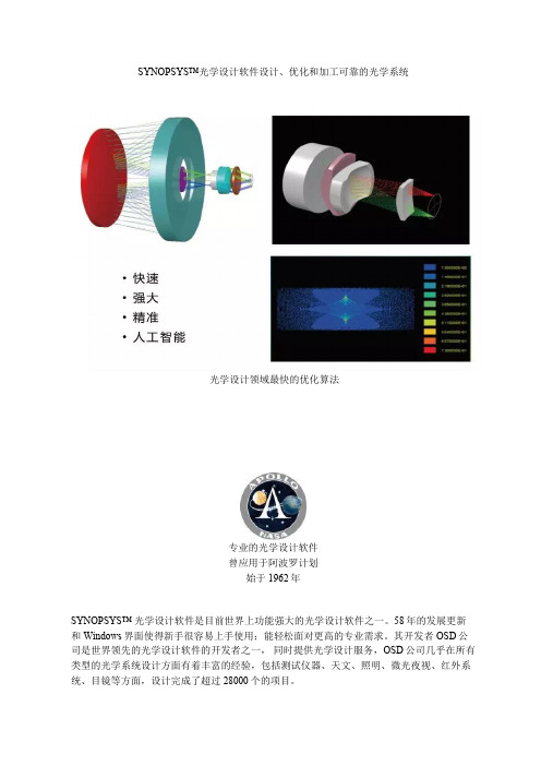
SYNOPSYS™光学设计软件设计、优化和加工可靠的光学系统光学设计领域最快的优化算法专业的光学设计软件曾应用于阿波罗计划始于1962年SYNOPSYS™ 光学设计软件是目前世界上功能强大的光学设计软件之一。
58年的发展更新和Windows界面使得新手很容易上手使用;能轻松面对更高的专业需求。
其开发者OSD公司是世界领先的光学设计软件的开发者之一,同时提供光学设计服务,OSD公司几乎在所有类型的光学系统设计方面有着丰富的经验,包括测试仪器、天文、照明、微光夜视、红外系统、目镜等方面,设计完成了超过28000个的项目。
光刻镜头从1976年以来,全球的用户已成功地利用SYNOPSYS™设计研制了大量镜头,受到广大客户的肯定和好评。
SYNOPSYS™可以分析优化各种各样的复杂光学系统。
支持多种特殊光学面如衍射光学元件、复杂非球面、自由曲面设计、各种变焦镜头,扫描系统。
很容易实现元件的偏心和倾斜;广角镜头非球面相机镜头美国Optical Systems Design(LLC简称OSD),作为一个光学设计服务和软件开发商,五十多年来一直孜孜不倦地在时间范围内推动创新光学技术的发展。
目前OSD公司是世界最大的光学设计软件供应商,发展了国际领先的光学设计软件——SYNOPSYS™光学设计软件。
客户遍布全世界25个国家和地区。
OSD公司可以快速有效地解决用户的设计需求、概念发展或方案开发、详细的镜头设计、公差分析、技术性能分析(包括衍射效应,通过Monte-Carlo 分析公差预算影响);建立的透镜系统会自动匹配首选供应商的光学样本列表,从而降低加工成本和加快设计加工进程。
反射式系统--------------------------------------初始结构:专利文件和优良设计起始点:专家系统工具XSYS可以存储并使用来自设计良好的光学结构。
输入所要设计的系统的使用波长、相对孔径、视场等参数,软件即可从自带的镜头库中找出对应的结构以供选择。
Synopsys发布DesignWare DDR4存储器接口IP

Synopsys发布DesignWare DDR4存储器接口IP亮点:· Synopsys扩展了其业界领先的DesignWare® DDR存储器接口知识产权(IP)系列,以使其亦可支持DDR4 SDRAM· 对DDR3和LPDDR2/3移动SDRAM的向后兼容性,为SoC设计师在从一种SDRAM标准向下一种标准过渡时带来了灵活性· 新推出的DDR4 IP可提供更多功能,同时与其前一代产品相比,延迟降低高达50%· DDR4内存控制器和PHY之间由一种标准的DFI3.1接口连接,以使各种定制的PHY和控制器之间的连接变得更加流畅全球领先的电子器件和系统设计、验证和制造软件及知识产权(IP)供应商新思科技公司(Synopsys, Inc.,纳斯达克股票市场代码:SNPS)日前宣布:其DesignWare DDR接口IP产品组合已经实现扩充,以使其包括了对基于新兴的DDR4标准的下一代SDRAM。
通过在一个单内核中就实现对DDR4、DDR3以及LPDDR2/3的支持,DesignWare DDR解决方案使设计师能够在相同的系统级芯片(SoC)中,实现与高性能或者低功耗SDRAM的连接,它已经成为诸如用于智能手机和平板电脑的应用处理器等等许多SoC的一项关键需求。
“Synopsys对DDR4内存的支持,对构建一个强大的DDR4生态系统是一项重大贡献,”美光科技公司DRAM市场营销副总裁Robert Feurle说道。
“DDR4为业界带来了实实在在的功耗与性能优势,而美光正在雄心勃勃地推进DDR4的导入。
通过实现其规划的具备向后兼容性的DesignWare DDR接口IP,Synopsys将使芯片开发者能够架起从今天基于DDR3的SoC过渡到即将来临的DDR4设计的桥梁。
Synopsys系列工具简介
Synopsys系列工具简介Synopsys的产品线覆盖了整个IC设计流程,使客户从设计规范到芯片生产都能用到完备的最高水平设计工具。
公司主要开发和支持基于两个主要平台的产品,Galaxy设计平台和Discovery验证平台。
这些平台为客户实现先进的集成电路设计和验证提供了整套综合性的工具。
Synopsys解决方案包括:System Creation(系统生成)System Verification and Analysis(系统验证与分析)Design Planning(设计规划)Physical Synthesis(物理综合)Design for Manufacturing(可制造设计)Design for Verification(可验证设计)Test Automation(自动化测试)Deep Submicron, Signal and Layout Integrity(深亚微米技术、信号与规划完整性技术)Intellectual Property and Design Reuse Technology(IP 核与设计重用技术)Standard and Custom Block Design(标准和定制模块设计)Chip Assembly(芯片集成)Final Verification(最终验证)Fabrication and Packaging(制造与封装设计工具)Technology CAD(TCAD)(工艺计算机辅助设计技术)主要包括以下工具:1.VCS (Verilog Compiled Simulator)2.DC (Design Compiler)3.ICC (IC Compiler)4.PT (PrimeTime)5.Hercules (Hercules Physical Verification)6.Star-RCXT (parasitic extraction tool)7.LEDA (LEDA Checker and LEDA Specifier)8.Formality (RTL to gate-level equivalence checking of cell-based designs)9.TetraMAX ATPG (Provides manufacturing test patterns for scan designs)1.VCS (Verilog Compiled Simulator)VCS是编译型Verilog模拟器,它完全支持OVI标准的Verilog HDL语言、PLI和SDF。
synopsys产品线介绍.docx

Synopsys产品线介绍目录DC Ultra (1)DesignWare Library (DesignWare库) (2)DFT Compiler (2)TetraMAX ATPG (3)Apollo-II (3)Star-RCXT (4)Hercules (4)PrimeTime (5)VCS (5)Vera (6)LEDA (6)Cosmos-Scope (7)DC UltraDesign Compiler的最高版本在Synopsys软件中完整的综合方案的核心是DC UltraTM,对所有设计而言它也是最好级别的综合平台。
DC Ultra添加了全面的数据通路和时序优化技术,并通过工业界的反复证明。
DC Ultra具有独特的优化技术,能满足今天设计的各种挑战。
DC Ultra提供快速的具有先进水平的数据通路优化技术,能建立快速关键路径时序。
另外,DC Ultra采用后布局和优化布线技术,易于较快达到时序收敛。
DC Ultra已在工业界确立了领先地位,DC Ultra综合引擎能提供DC Expert 所有的功能,以及它的独特的优点。
能与DC Ultra共同工作的软件有路径综合、测试综合和功耗优化、静态时序和功耗分析,以及经验证的、高性能Design Ware库。
这是经过验证的技术独特的集成,形成一个完整的综合解决方案,能在最短的时间里满足用户所有的设计挑战。
●对数据通路设计的面积和时序方面,提交最好质量的设计结果●对时序要求很高的设计, 提供最好的电路性能●与测试和功耗综合紧密结合,以提供最高的设计效率,并致力于实现所有综合的目标●对那些需要多次反复设计流程才能达到时序收敛的设计,通过提供和布局布线环境的紧密衔接,有助于快速实现设计的多时序收敛●来自于超过50个硅片和库的供应商可应用的大于500个综合库DesignWare Library (DesignWare库)DesignWare Library包含了最常用的结构以外的IP,这对于设计开发ASIC和SOC来讲是必要的。
Synopsys提供业界最完整的IP产品组合来加速物联网设计的开发

Synopsys提供业界最完整的IP产品组合来加速物联网设计的开发新思科技(Synopsys,Inc.,纳斯达克股票代码:SNPS)日前宣布:推出一套完整的、经优化的知识产权(IP)产品组合,以满足多样化物联网应用对安全、无线连接、能效和传感器处理等要求,这些应用诸如可穿戴设备、智能家电、计量和无线传感器网络等。
用于物联网的DesignWare®IP产品组合包括功耗和面积都经过优化的逻辑库、存储器编译器、非易失性存储器(NVM)、数据转换器、有线和无线接口IP、安全IP、超低功耗处理器内核,以及整合型传感器和控制IP子系统。
此外,Synopsys的embARC Open Software Platform开放软件平台提供了对开源和商业驱动软件、操作系统和中间件的在线获得,以加速应用软件的开发。
通过提供为物联网而优化的、业界最丰富的IP产品组合和软件解决方案,Synopsys 使开发人员能够加速物联网系统的开发。
为物联网而优化的IP解决方案· 近阈值、超高密度逻辑库降低了功耗,同时厚氧化层逻辑库为永远开启功能保证低漏电· 高密度、低电压嵌入式存储器编译器使用了最小位单元,并集成了可支持嵌入式闪存的测试与修复功能· 功耗和面积都经优化的12位/14位SAR数据转换器、USB 1.1和USB 2.0、MIPI CSI-2和DSI,以及NVM 等IP,能够实现所要求的传感器、数据和连接功能,同时降低总体系统成本· 经硅验证的Bluetooth® Smart IP符合Bluetooth 4.0、4.1和4.2低功耗标准,并支持低至一伏特的运行,以实现更长的电池续航时间· 安全IP产品包括Public Key Accelerators(公开密钥加速器)、True Random Number Generators(真随机数生成器)、安全协议加速器,以及安全硬件root of trust、安全启动和中间件软件,它们可针对物联网领域中不断演变的威胁来提供安全保护· 高度可配置的32位DesignWare ARC®嵌入式处理器和EV视觉处理器使设计人员能够定制每个ARC处理器模块,以满足物联网应用特定的性能、功耗和面积要求· 预先验证过的、紧密集成的传感器和控制IP子系统借助针对应用的硬件加速器,可实现显著的功耗节约,以及周期数成倍的减少软件开发工具和生态系统Synopsys提供一套完整的商业和开源工具及软件套件,以加速用于物联网的、基于ARC处理器的嵌入式系统的开发。
Synopsys 实验系列12_高速模拟电路设计与验证_Hspice
Capacitor Diode Dependent Sources Current JFET or MESFET Mutual Inductor Inductor MOSFET BJT Resistor Transmission Line Voltage Source Sub circuit Call
2011.1.5
ASIC设计中心
Hspice 运行 输入输出
Star-Hspice Input Input netlist Model /libraries Star-Hspice Output Run status Output listing Analysis data, transient Analysis data, dc Analysis data, ac Measure output .sp .inc, .lib .st0 .lis .tr# (e.g. .tr0) .sw# (e.g. .sw0) .ac# (e.g. .ac0) .m*# (e.g. .mt0)
ASIC设计中心
Lab1
2011.1.5
ASIC设计中心
输出 输出命令包括: .PRINT、.PLOT、.GRAPH、.PROBE 和.MEASURE。
.PLOT antype ov1 <ov2...> <plo1,phi1...plo32,phi32> .PROBE antype ov1<ov2...ov32> .PRINT antype ov1 <ov2...ov32>
2011.1.5
ASIC设计中心
Lab1
Lab1 一个简单例子 * lab1 an example .options list node post .op .ac dec 10 1k 1meg .print ac v(1) v(2) i(r2) i(c1) v1 1 0 10 ac 1 r1 1 2 1k r2 2 0 1k c1 2 0 .001u .end
EDA技术_Synopsys公司STA工具PrimeTime介绍
PT进行时序分析的流程 进行时序分析的流程
EDA技术实验 技术实验
设置设计环境
设置查找路径和链接路径
The search_path variable specifies a list of directory paths thatPrimeTime uses to find the designs, libraries, and other files. The link_path variable specifies a list of libraries that PrimeTime uses to link designs
pt_shell> create_generated_clock -multiply_by 2 -duty_cycle 60 -source [get_pins CLK] [get_pins foo1]
2010-12-29
16
ASIC设计中心
PrimeTime命令 命令
EDA技术实验 技术实验
时序分析命令
set_operating_conditions set_case_analysis read_sdf read_parasitics set_driving_cell set_load set_wire_load_model set_multicycle_path set_false_path set_disable_timing
pt_shell>set_case_analysis 1 test_mode pt_shell>remove_case_analysis test_mode
2010-12-29
7
ASIC设计中心
synopsys ic compiler 介绍、安装、调试和设计流程

synopsys ic compiler 介绍、安装、调试和设计流程加入该小组相关分类:petery (组长) 2007/9/23 顶楼举报一、介绍synopsys ic compiler (v2005.linux)是基于Galaxy设计平台开发的产品。
主要的工具有:LEDALEDA是可编程的语法和设计规范检查工具,它能够对全芯片的VHDL和Verilog描述、或者两者混合描述进行检查,加速SoC的设计流程。
LEDA预先将IEEE可综合规范、可仿真规范、可测性规范和设计服用规范集成,提高设计者分析代码的能力VCSVCS是编译型Verilog模拟器,它完全支持OVI标准的Verilog HDL语言、PLI和SDF。
VCS具有目前行业中最高的模拟性能,其出色的内存管理能力足以支持千万门级的ASIC设计,而其模拟精度也完全满足深亚微米ASIC Sign-Off 的要求。
VCS结合了节拍式算法和事件驱动算法,具有高性能、大规模和高精度的特点,适用于从行为级、RTL到Sign-Off等各个阶段。
VCS已经将CoverMeter 中所有的覆盖率测试功能集成,并提供VeraLite、CycleC等智能验证方法。
VCS 和Scirocco也支持混合语言仿真。
VCS和Scirocco都集成了Virsim图形用户界面,它提供了对模拟结果的交互和后处理分析。
SciroccoScirocco是迄今为止性能最好的VHDL模拟器,并且是市场上唯一为SoC验证度身定制的模拟工具。
它与VCS一样采用了革命性的模拟技术,即在同一个模拟器中把节拍式模拟技术与事件驱动的模拟技术结合起来。
Scirocco的高度优化的VHDL编译器能产生有效减少所需内存,大大加快了验证的速度,并能够在一台工作站上模拟千万门级电路。
这一性能对要进行整个系统验证的设计者来说非常重要。
VeraVera验证系统满足了验证的需要,允许高效、智能、高层次的功能验证。
加速ASIC原型验证 Synopsys的HAPS-80提供高达100MHz性能

加速ASIC原型验证 Synopsys的HAPS-80提供高达100MHz性能原型验证的挑战现在做产品时,人们不仅关注ASIC本身,对软件平台更关注。
因此设计送到Fab(芯片厂)生产之前,要做一些早期的原型认证。
无论是ASIC设计者还是原型认证平台的开发者,现在关注两方面。
图:HAPS硬件和ProtoCompiler软件首先是性能,最终产品可能要跑到GHz的频率,而且很多客户的项目时间越来越短,有些只有1年或6个月时间。
在原型认证平台方面,人们期待高性能的软件开发,而目前市场上只是几十M、上百M赫兹的产品。
另外,产品要接近最终产品的真实性,所以现在从原型验证的需求上看,无论是软件工具还是硬件设备,市场上的产品组合很多也很复杂,所以如何选择也很重要。
图:市面上的物理原型产品组合多且复杂Synopsys 资深产品市场经理Neil Songcuan先生称,Synopsys可以提供一站式的解决方案,不仅可以避免各种不确定性,而且集成化的HAPS硬件和ProtoCompiler软件将首款原型的完成时间缩短为不到2周。
HAPS-80优势分析· 基于FPGA的HAPS-80原型系统结合ProtoCompiler软件,提供高达100MHz的多FPGA 性能,以及全新的、自动化的引脚高速时分复用;· ProtoCompiler软件专用于HAPS系统,自动化分区使首款原型的完成时间缩短为平均不到两周;· HAPS-80企业级配置采用赛灵思(Xilinx)Virtex UltraScale FPGA芯片,可支持高达16亿个专用集成电路(ASIC)逻辑门,并支持面向并行设计执行的远程使用和多设计模式;· 内置调试功能,能够捕获到数千个RTL信号,由工具自动插入,实现更高的调试效率和可见度;· 作为Synopsys Verification Continuum平台的一部分,VCS仿真结合Unified Compile以及Verdi调试结合Unified Debug简化了在仿真、模拟和原型之间的移植,使设计和验证的启动时间缩短了数月。
Synopsys推出快速原型系统HAPS-60系列
在本次会议 中 ,参会者将会亲临现场 见证安捷伦科技
7 年 的技 术 飞 跃 与 烁 世 贡 献 。从 “ 在 网络 ”的全 面测 试 方 0 泛
案 ,到 3 4 G- G的 无线测试大全 ;从高速数字技术的深入解
得可 Po lw T rFo @A x系统 能满足
现 实 的 大 规模 复 杂 生 产 要 求
讨大会。 ( 本刊 通 讯 员)
产和产品管理专 家 ,这家 电子公司具有相 当严格的评估标
准 ,而 DE 的 系 统 不 仅 达 到 甚 至 在 一 些 地 方 超 越 了客 户 的 K
要求。
S n p y 推 出快速 原型 系统 y o ss
H S6 AP .0系 列
全球 领先的半导体设计 、验证和造软件及知识 产权
误 ,显 著 缩 短处 理不 规 则 B A 所 需 的 时 间 。 G
锡膏的浪费量在一个星 期内减少 了210 , 0 g 在大规 模生产环 境下 ,这是一个相 当理想的数字。使用得可 Ha k y 。 w E e 印刷 后检测工具 , 印刷产量超过每张 电路板 1s 4 这个 目标 达 1%。 0
域。 ( 本刊 通 讯 员)
2 6日在北京新 云南皇冠假 日酒店盛大召开。本次测试测量
大会还会先后在 中国深圳 、中国台湾 ( 台北和新竹 ) 、韩 国 ( 首尔 ) 、印度 ( 班加 罗尔和新德里 ) 、马来西亚 ( 槟城 )和
新 加 坡 等 地 相 继 举 行 , 创亚 洲 地 区最 大 的 测 试 测 量科 技 年 开 度盛会 。
DE K的 Po lw封闭式印刷头技术 ,在经过一段成功 rFo 的测试期后 ,因其杰 出的表 现能满足复杂 的大规模生产要 求, 为一家知名的 电子解决方案公司所采用。作为设计 、 生
EDA技术_Synopsys公司逻辑综合工具DC介绍 part1
1)、DC的安装目录; 2)、用户的home目录; 3)、当前启动目录。
注意:后装载的启动文件中的设置将覆盖先装载的启 动文件中的相同设置。
2013-7-9
22
(四)DC的基本概念(续)
EDA技术实验
系统库变量
search_path定义库文件所在的搜索路径 目标库(targe_library):是DC在mapping时将设计映射到特 定工艺所使用的库,就是使用目标库中的元件综合成设计的门 级网表 连接库(link_library):是提供门级网表实例化的基本单元, 也就是门级网表实例化的元件或单元都来自该库。连接库定义 为标准单元的db格式的库文件加上pad db格式的库文件,加上 ROM,RAM等宏单元库文件 synthetic_library是综合库,它包含了一些可综合的与工艺无关 的IP。dw_foundation.sldb是Synopsys提供的名为Design Ware的 综合库,它包含了基本的算术运算逻辑、控制逻辑、可综合存 储器等IP,在综合时调用这些IP有助于提高电路性能和减少综 合时间。 符号库(symbol_library):是工艺库元件的图形符号表示,用 来图形化显示生成的门级网表。
Synopsys TIS Pro 产品介绍说明书

PRODUCT FEATURESDescript ionSynopsys TIS P ro is an optical scattering inst rument for effic ientmeasurements of reflectance, transmittance, and absorption . This fully automated dev ice features an integrated sph ere and spectra l detector assembled in a housing that c ontrols stray lig ht to ensure fas t, accuratemeasurement r esults. Synopsy s TIS Pro deter mines the optic al properties of surfaces and m aterials and pro vides measure ments over the entire visible spectrum at va rious angles of incidence.Synopsys TIS P ro can be used in conjunction with Synopsys Mini-Diff and REFLET 180S p roducts to prov ide a complete , end-to-end so lution that fully characterizes s cattering prope rties of surface s and materials , including bi-directional s cattering distrib ution function (BSDF) and tota l integrated scattering (TIS ) data.Measurement d ata from Synop sys TIS Pro can be imported in to optical desig n software tools to provide reali stic simulation s of your as-built product.Figure 1: Synops ys TIS Pro housin g and instrumen t (prototype pictu red does notnecessarily repre sent the final des ign)Features at a Glance•Practical instrument for accurateoptical scattering measurements over the entire visible spectrum at multiple angles of incidence•Provides reflectance, transmittance, and absorption measurements of surfaces and materials used in optical systems •Designers can import the measurement data into Synopsys optical software tools for high-accuracy product simulationsHow Synopsys TIS Pro WorksOnce you have placed a surface or material sample in the instrument, use the Synopsys TIS Pro software to specify the angles of incidence to measure and start the measurement. The rotation stages from the source and sample will rotate accordingly. Synopsys TIS Pro will then aim light onto the sample and its spectral detector will collect the signal exiting the integrating sphere for the specified positions.Using a standard calibration measurement, the Synopsys TIS Pro software will post-process and compute the reflectance,transmittance, and absorption values of the sample. You can display, save, and export this data to optical design software for high-accuracy product simulations.No SampleReference MeasurementSample MeasurementSampleFigure 2: Synopsys TIS Pro software and transmittance measurement principleApplication ExamplesSynopsys TIS Pro is ideal for assessing the effects of surfaces and materials in optical systems.•Characterize reflector/diffuser materials for automotive design or general lighting systems• Evaluate quality controls in production• Analyze stray light suppression from coatings used in aerospace optics • Measure spectral behavior to incorporate in photorealistic renderings • Study optical properties of cosmetics• Characterize materials for many incident anglesContact us to request a demo of these and other application examples.REFLECTANCE ABSORBANCE TRANSMITTANCEFigure 3: TIS ratio grade exampleSpectral MeasurementsSynopsys TIS Pro uses a halogen source and a spectral detection for both reflectance and transmittance. It allows a full wavelength-dependent measurement. Results are displayed in a 2D plot within the software (TIS values against wavelength for different angles of incidence).Figure 4: Example of green sample spectral reflectanceReflective MaterialsSynopsys TIS Pro provides TIS measurements including reflectance for several incident angles over the entire visible spectral range.• After a two-step calibration (one step for dark signal to offset stray light and one step with a known reference standard to calibrate the response of the spectrophotometer), it is possible to measure:–Reflectors, such as aluminum for general lighting–Paints for automotive or cosmetic applications–Diffusing material sockets–Optical mounts and more, including space optics• The measured reflectance values can be saved as text files–TIS comparison can be made directly from the software for comparison between samples–Synopsys TIS Pro software also accounts for anisotropic material measurementExample: Black CoatingReflector materials can have complex behavior depending on the incident plane. The Synopsys TIS Pro allows you to capture reflective properties for various angles of incidence.Figure 5: Example of black sample reflectance spectrumTransmissive MaterialsSynopsys TIS Pro provides TIS measurements including transmittance for several incident angles over the entire visiblespectral range.• The same source is used for transmittance and reflectance measurements• After a two-step calibration (one step for dark signal to offset stray light and one step with no sample to calibrate the response of the spectrophotometer), it is possible to measure diffusing materials such as:–Dichroic filters–Colored diffusing plastics–Opal glassFigure 6: Example of transmissive materials measurementReflective and Transmissive MaterialsSynopsys TIS Pro provides absorption measurements on diffusers and can create a ready-to- use reflectance and transmittance (RT) file for use in illumination design software and photorealistic simulations.Figure 7: Synopsys TIS Pro data can be used to enhance photorealistic renderings of your product designs ComponentsSynopsys TIS Pro includes:• One calibration sample• Integrated software• High-precision spectrophotometer• Barium sulfate coated sphere• Stray light reduction housingTechnical SpecificationFor more information about Synopsys Optical Solutions, visit /optical-solutions.html or send an email to*******************.©2022 Synopsys, Inc. All rights reserved. Synopsys is a trademark of Synopsys, Inc. in the United States and other countries. A list of Synopsys trademarks isavailable at /copyright.html. All other names mentioned herein are trademarks or registered trademarks of their respective owners.。
EDA技术_Synopsys公司逻辑综合工具DC 介绍 part2
2013-7-9
21
Synopsys工艺库—功能、时序等 属性信息
2013-7-9
22
Synopsys工艺库——逻辑库
EDA技术实验
延时计算 Synopsys支持的延迟模型有:
CMOS通用的延迟模型 CMOS分段的线性延迟模型 非线性的查找表延迟模型
DSM的设计,前两种延迟模型不常用, 非线性延迟模型以输入的跃迁时间和输出 的容性负载为参变量计算延迟的时间值, 其结果以表格的形式列出供DC查找。
2013-7-9
12
Design Compiler Interfaces
EDA技术实验
1) dc_shell-t(DC-Tcl)
2) dc_shell(DCSH)
3) Design Analyzer
4) Design vision
in 2000.11 release
2013-7-9
13
CONTENTS
2013-7-9
18
Synopsys工艺库——逻辑库
EDA技术实验
环境描述:用于对PVT的偏差建模。
工作条件(operating conditions) 线负载模型(WLM, wire load model) 时序范围模型
2013-7-9
19
Synopsys工艺库——逻辑库
EDA技术实验
工作条件(operating conditions):指 定了工艺、温度、电压以及RC树模型, 用于设计的综合和时序分析。例如:
2013-7-9 23
Synopsys工艺库——逻辑库
EDA技术实验
设计人员了解工艺库,在于正确使用和 理解逻辑库,而不在于与库设计者相关的 细节上。
新思科技推出IC Validator NXT

新思科技推出IC Validator NXT新思科技(Synopsys)是一家全球领先的电子设计自动化(EDA)和半导体IP公司,致力于为半导体行业提供先进的设计和验证解决方案。
最近,新思科技推出了ICValidator NXT,这是一款全新的物理验证平台,旨在加速异质集成电路(IC)设计的验证进程,提高设计的质量和生产效率。
IC Validator NXT的主要特点包括:1. 充分利用多核处理技术:IC Validator NXT充分利用了多核处理技术,实现了卓越的性能和可伸缩性。
通过利用多核处理器的并行计算能力,IC Validator NXT可以在短时间内处理大规模复杂设计的物理验证,极大地提高了验证效率和生产力。
2. 高效的物理验证引擎:IC Validator NXT具有高效的物理验证引擎,可以快速而准确地检测设计中的物理错误和潜在问题。
该引擎采用了先进的验证算法和技术,能够在设计的不同阶段对布图进行全面的物理验证,从而确保设计的准确性和可靠性。
3. 先进的制造规则检查(DRC)和物理验证检查(LVS)功能:IC Validator NXT提供了先进的DRC和LVS功能,可以帮助设计团队在不同制造工艺下快速准确地进行设计规则检查和电路布局检查。
这些功能对于保证设计的芯片制造质量和可靠性至关重要,IC Validator NXT通过高效的算法和技术,能够满足不同制造工艺下的复杂设计验证需求。
4. 完善的用户界面和工作流程:IC Validator NXT提供了完善的用户界面和工作流程,为设计团队提供了直观友好的操作环境和灵活便捷的工作流程。
设计人员可以通过简单直观的方式进行设计规则的设置、物理验证的配置和结果的分析,同时还能够实现与其他设计工具和流程的无缝集成。
IC Validator NXT的推出,得到了全球范围内众多半导体公司和设计团队的积极响应和认可。
许多行业领先的半导体公司已经选择了IC Validator NXT作为他们的首选物理验证平台,并取得了显著的验证效果和设计成果。
新思科技 DesignWare 嵌入式 USB 2.0 解决方案说明书

DESIGNWARE IP数据手册/designware 简介借助DesignWare® 嵌入式USB 2.0 (eUSB2) PHY、eUSB2中继器、USB数字控制器、验证IP和IP子系统方面的专业知识,新思科技为设计人员提供了适用于低功耗移动和消费类产品的USB 2.0 IP解决方案,例如采用业界最先进工艺节点设计的智能手机、平板电脑、笔记本电脑、游戏和 AR/VR,以及无线设备。
USB Type-C“Chip to World”“Chip to World”图1:eUSB2用例业内最先进的工艺节点不支持USB 2.0规范要求的3.3V信号和5V容限。
3.3V 信号最初在1994年的USB 1.0规范中定义,需要向后兼容。
eUSB2 规范为低功耗芯片间通信定义了新的更低电压的USB信号。
eUSB2中继器在标准USB 2.0和eUSB2信号电平之间转换,允许旧有USB 2.0设备与配有eUSB2 PHY的片上系统 (SoC) 连接。
DesignWare USB IP的设计依托客户多年来使用新思科技通过硅晶验证的USB PHY产品线取得的成功,而且该产品线已移植到180nm 到 5nm 的100多个工艺节点中。
通过与DesignWare主机、设备或双角色数字控制器结合使用,并使用新思科技的验证IP进行验证,DesignWare eUSB2 IP可为高级SoC设计提供完整的USB 2.0解决方案。
要点• 符合eUSB2 1.1规范• 可用于USB主机、设备和双角色应用中• eUSB2 PHY和eUSB2中继器支持 USB2.0 480Mbps(高速)、12Mbps(全速)和 1.5Mbps(低速)数据速率• eUSB2 PHY专为不支持3.3V信号和5V容限的最先进工艺节点而设计• eUSB2 PHY接口:UTMI+ 3级规范• eUSB2中继器专为支持3.3V信号和5V容限的成熟工艺节点而设计目标应用• 智能手机• 平板电脑• 轻薄型 PC 和混合型 PC• 笔记本和台式电脑• 游戏、AR/VR• 高级无线设备(5G调制解调器、WiFi 6)技术• eUSB2 PHY: 5nm, 7nm• USB2中继器:28nm eUSB2 IP解决方案eUSB2 PHY IP特性• 专为高级工艺节点(7nm及以下)设计• 最大限度地减少由于工艺、电压、温度、封装和板卡寄生参数的变化而产生的影响• 支持USB 2.0 480Mbps(高速)、12Mbps(全速)和1.5Mbps(低速)数据速率• 与新思科技的DesignWare USB 2.0、3.0、3.1和3.2主机、设备及双角色控制器连接• 最低功耗:对于用于eUSB2 芯片间通信的高级移动设备,可延长电池寿命Transceiver Common图2:eUSB2 PHY框图eUSB2中继器IP特性• 在eUSB2和USB 2.0信号电平间转换,使配有eUSB2 PHY的SoC能够与旧有USB 2.0产品连接• 专为成熟工艺节点而设计• 可集成到PMIC、音频、Wi-Fi、组合式无线芯片中,或作为独立(多端口)中继器芯片实施• 支持USB 2.0 480Mbps(高速)、12Mbps(全速)和1.5Mbps(低速)数据速率• 高级内置自检 (BIST)、可调性和诊断图3:eUSB2中继器框图2USB控制器IP特性• DesignWare USB 2.0、3.0、3.1和3.2数字控制器与DesignWare eUSB2 PHY兼容验证IP特性• 支持USB 3.2、3.1、3.0、2.0和 eUSB2• 100%原生SystemVerilog• 主机、设备和集线器仿真• 内置覆盖和验证计划• 全面的回调、消息处理和错误注入• 与Verdi Protocol Analyzer 3集成• 协议层–控制、中断和ISOC–数据突发–SuperSpeed批量数据流–LMP、SOF和ITP生成• 链路层–具有完全控制权的L TSSM可在任何状态启动–SuperSpeed电源管理–电缆连接和断开–速度增大和减小–测试模式• PHY层–SuperSpeed PIPE,与时钟恢复同步–USB 2.0 UTMI、ULPI接口IP子系统专业知识特性• 通过新思科技IP协议和SoC设计专家根据独特的SoC要求而配置和定制USB子系统,满足严格的项目进度要求• 通过专门针对SoC集成的子系统和验证测试,最大限度地减少子系统集成工作量同时使设计人员能够专注于发挥关键技能• 降低总体开发成本,©2021 Synopsys, Inc. All rights reserved. Synopsys is a trademark of Synopsys, Inc. in the United States and other countries. A list of Synopsys trademarksis available at /copyright.html . All other names mentioned herein are trademarks or registered trademarks of their respective owners.08/31/21.CS743817698 eUSB2 DS simplified chinese.。
Synopsys DesignWare IP for HPC SoCs 2说明书
DesignWare IP for Cloud Computing SoCs2High-Performance ComputingToday’s high-performance computing (HPC) solutions provide detailed insights into the world around us and improve our quality of life. HPC solutions deliver the data processing power for massive workloads required for genome sequencing, weather modeling, video rendering, engineering modeling and simulation, medical research, big data analytics, and many other applications. Whether deployed in the cloud or on-premise, these solutions require high performance and low-latency compute, networking, and storage resources, as well as leading edge artificial intelligence capabilities. Synopsys provides a comprehensive portfolio of high-quality, silicon-proven IP that enables designers to develop HPC SoCs for AI accelerators, networking, and storage systems.Benefits of Synopsys DesignWare IP for HPC• Industry’s widest selection of high-performance interface IP , including DDR, PCI Express, CXL, CCIX, Ethernet, and HBM, offers high bandwidth and low latency to meet HPC requirements• Highly integrated, standards-based security IP solutions enable the most efficient silicon design and highest levels of data protection• Low latency embedded memories with standard and ultra-low leakage libraries, optimized for a range of cloud processors, provide a power- and performance-efficient foundation for SoCsIP for HPC SoCs in Cloud ComputingOverviewHyperscale cloud data centers continue to evolve due to tremendous Internet traffic growth from online collaboration, smartphones and other IoT devices, video streaming, augmented and virtual reality (AR/VR) applications, and connected AI devices. This is driving the need for new architectures for compute, storage, and networking such as AI accelerators, Software Defined Networks (SDNs), communications network processors, and solid state drives (SSDs) to improve cloud data center efficiency and performance. Re-architecting the cloud data center for these latest applications is driving the next generation of semiconductor SoCs to support new high-speed protocols to optimize data processing, networking, and storage in the cloud. Designers building system-on-chips (SoCs) for cloud and high performance computing (HPC) applications need a combination of high-performance and low-latency IP solutions to help deliver total system throughput. Synopsys provides a comprehensive portfolio of high-quality, silicon-proven IP that enables designers to develop SoCs for high-end cloud computing, including AI accelerators, edge computing, visual computing, compute/application servers, networking, and storage applications. Synopsys’ DesignWare ® Foundation IP , Interface IP , Security IP , and Processor IP are optimized for high performance, low latency, and low power, while supporting advanced process technologies from 16-nm to 5-nm FinFET and future process nodes.3Benefits of Synopsys DesignWare IP for AI Accelerators• Industry’s widest selection of high-performance interface IP , including DDR, USB, PCI Express (PCIe), CXL, CCIX, Ethernet, and HBM, offers high bandwidth and low latency to meet the high-performance requirements of AI servers• Highly integrated, standards-based security IP solutions enable the most efficient silicon design and highest levels of data protection• Low latency embedded memories with standard and ultra-low leakage libraries, optimized for a range of cloud processors, provide a power- and performance-efficient foundation for SoCsArtificial Intelligence (AI) AcceleratorsAI accelerators process tremendous amounts of data for deep learning workloads including training and inference which require large memory capacity, high bandwidth, and cache coherency within the overall system. AI accelerator SoC designs have myriad requirements, including high performance, low power, cache coherency, integrated high bandwidth interfaces that are scalable to many cores,heterogeneous processing hardware accelerators, Reliability-Availability-Serviceability (RAS), and massively parallel deep learning neural network processing. Synopsys offers a portfolio of DesignWare IP in advanced FinFET processes that address the specialized processing, acceleration, and memory performance requirements of AI accelerators.IP for Core AI AcceleratorBenefits of Synopsys DesignWare IP for Edge Computing• Industry’s widest selection of high-performanceinterface IP , including DDR, USB, PCI Express, CXL, CCIX, Ethernet, and HBM, offers high bandwidth and low latency to meet the high-performance requirements of edge computing servers• Highly integrated, standards-based security IP solutions enable the most efficient silicon design and highest levels of data protection• Low latency embedded memories with standard and ultra-low leakage libraries, optimized for a range of edge systems, provide a power- and performance-efficient foundation for SoCsIP for Edge Server SoCEdge ComputingThe convergence of cloud and edge is bringing cloud services closer to the end-user for richer, higher performance, and lower latency experiences. At the same time, it is creating new business opportunities for cloud service providers and telecom providers alike as they deliver localized, highly responsive services that enable new online applications.These applications include information security, traffic and materials flow management, autonomous vehicle control, augmented and virtual reality, and many others that depend on rapid response. For control systems in particular, data must be delivered reliably and with little time for change between data collection and issuing of commands based on that data.To minimize application latency, service providers are moving the data collection, storage, and processing infrastructure closer to the point of use—that is, to the network edge. To create the edge computing infrastructure, cloud service providers are partnering with telecommunications companies to deliver cloud services on power- and performance-optimized infrastructure at the network edge.ServersThe growth of cloud data is driving an increase in compute density within both centrally located hyperscale data centers and remote facilities at the network edge. The increase in compute density is leading to demand for more energy-efficient CPUs to enable increased compute capability within the power and thermal budget of existing data center facilities. The demand for more energy-efficient CPUs has led to a new generation of server CPUs optimized for performance/watt.This same increase in data volume is also driving demand for faster server interfaces to move data within and between servers. Movement of data within the server can be a major bottleneck and source of latency. Minimizing data movement as much as possible and providing high-bandwidth, low-latency interfaces for moving data when required are key to maximizing performance and minimizing both latency and power consumption for cloud and HPC applications. To improve performance, all internal server interfaces are getting upgrades:• DDR5 interfaces are moving to 6400 MBps• Doubling the bandwidth of PCIe interfaces as they move from PCIe 4.0 at 16GT/s to PCIe 5.0 at 32GT/s and PCIe 6.0 at 64GT/s • Compute Express Link (CXL) provides a cache coherent interface that runs over the PCIe electrical interface and reduces the amount of data movement required in a system by allowing multiple processors/accelerators to share data and memory efficiently• New high-speed SerDes technology at 56Gbps and 112Gbps using PAM4 encoding and supporting protocols enable faster interfaces between devices including die, chips, accelerators, and backplanesCloud server block diagram Benefits of Synopsys DesignWare IP for Cloud Compute Servers• Silicon-proven PCIe 5.0 IP is used by 90% of leadingsemiconductor companies• CXL IP is built on silicon-proven DesignWare PCIExpress 5.0 IP for reduced integration risk and supports storage class memory (also referred to as persistentmemory) for speed approaching that of DRAM withSSD-like capacity and cost• 112Gbps XSR/USR SerDes supports a wide range ofdata rates (2.5 to 112 Gbps) with area-optimized RXVisual ComputingAs cloud applications evolve to include more visual content, support for visual computing has emerged as an additional function of cloud infrastructure. Applications for visual computing include streaming video for business applications, online collaboration, on-demand movies, online gaming, and image analysis for ADAS, security, and other systems that require real-time image recognition. The proliferation of visual computing as a cloud service has led to the integration of high-performance GPUs into cloud servers, connected to the host CPU infrastructure via high-speed accelerator interfaces.Server-based graphics accelerator block diagram45NetworkingTraditional data centers use a tiered network topology consisting of switched Ethernet with VLAN tagging. This topology only defines one path to the network, which has traditionally handled north-south data traffic. The transition to a flat, two-tier leaf-spine hyperscale data center network using up to 800G Ethernet links enables virtualized servers to distribute workflows among many virtual machines, creating a faster, more scalable cloud data center environment.Smart network interface cards (NICs) combine hardware, programmable AI acceleration, and security resources to offload server processors, freeing the processors to run applications. Integrated security, including a root of trust, protects coefficient and biometric data as it moves to and from local memories. Smart NICs accelerate embedded virtual switch, transport offloads, and protocol overlay encapsulation/decapsulation such as NVGRE, VXLAN and MPLS. By offering dedicated hardware offloads including NVMe-over-Fabric (NVMEoF) protocols, Smart NICs free the server CPU to focus compute cycles on cloud application software and enable efficient data sharing across nodes for HPC workloads.Network switch SoCs enable cloud data center top-of-rack and end-of-row switches and routers to scale port densities and speeds to quickly adapt to changing cloud application workloads. By scaling port speeds from 10Gb Ethernet to 400/800G Ethernet and extending port densities from dozens to hundreds of ports, the latest generation Ethernet switch SoCs must scale to provide lowest latency and highest throughput flow control and traffic management. Synopsys’ DesignWare Interface IP portfolio supports high-performanceprotocols such as Ethernet, PCI Express, CXL, CCIX, USB, DDR, and HBM. DesignWare Interface IP is optimized to help designers meet the high-throughput, low-latency connectivity needs of cloud computing networking applications. Synopsys’ Foundation IP offers configurable embedded memories for performance, power, and area, as well as high-speed logic libraries for all processor munication service providers are turning towards server virtualization to increase efficiency, flexibility, and agility tooptimize network packet processing. The latest communications architecture uses Open vSwitch Offloads (OVS), OVS over Data Plane Development Kits (DPDK), network overlay virtualization, SR-IOV, and RDMA to enable software defined data center and Network Function Virtualization (NFV), acceleratingcommunications infrastructure. To achieve higher performance, communications network processors can accelerate OVS offloads for efficiency and security. Synopsys provides a portfolio of high-speed interface IP including DDR, HBM, Ethernet for up to 800G links, CXL for cache coherency, and PCI Express for up to 64GT/s data rates. DesignWare Security IP enables the highest levels of security encryption, and embedded ARC processors offer fast, energy-efficient solutions to meet throughput and QoS requirements. Synopsys’ Foundation IP delivers low-latency embedded memories with standard and ultra-low leakage libraries for a range of cloud processors.IP for Smart NIC in cloud computing networkIP for cloud computing network switchIP for communication network processorsStorageNVMe-based Solid-State Drives (SSDs) can utilize a PCIe interface to directly connect to the server CPU and function as a cache accelerator allowing frequently accessed data, or “hot” data, to be cached extremely fast. High-performance PCIe-based NVMe SSDs with extremely efficient input/ output operation and low-read latency improve server efficiency and avoid having to access the data through an external storage device. NVMe SSD server acceleration is ideal for high transaction applications such as AI acceleration or database queries queries, as well as HPC workloads that require high-performance, low-latency access to large data sets. PCIe-based NVMe SSDs not only reduce power and cost but also minimize area compared to hard disk drives (HDDs). Synopsys’ portfolio of DesignWare Interface IP for advanced foundry processes, supporting high-speed protocols such as PCI Express, USB, and DDR, are optimized to help designers meet their high-throughput, low-power, and low-latency connectivity for cloud computing storage applications. Synopsys’ Foundation IP offers configurable embedded memories for performance, power, and area, as well as high-speed logic libraries for all processor cores. Synopsys also provides processor IP ideally suited for flash SSDs.Storage• High-performance, low-latency PCI Express controllersand PHYs supporting data rates up to 64GT/s enableNVMe-based SSDs• High-performance, low-power ARC processors supportfast read/write speeds for NVMe-based SSDs• Portfolio of interface IP including Ethernet, USB,PCI Express, and DDR provides low latency andfast read/write operationsFigure 6: IP for cloud computing storage6©2021 Synopsys, Inc. All rights reserved. Synopsys is a trademark of Synopsys, Inc. in the United States and other countries. A list of Synopsys trademarks is available at /copyright.html . All other names mentioned herein are trademarks or registered trademarks of their respective owners.05/04/21.CS610890866-SG Bro-Cloud Computing Brochure.。
Synopsys产品线介绍

S y n o p s y s产品线介绍 Ting Bao was revised on January 6, 20021Synopsys产品线介绍目录DC UltraDesign Compiler的最高版本在Synopsys软件中完整的综合方案的核心是DC UltraTM,对所有设计而言它也是最好级别的综合平台。
DC Ultra添加了全面的数据通路和时序优化技术,并通过工业界的反复证明。
DC Ultra具有独特的优化技术,能满足今天设计的各种挑战。
DC Ultra提供快速的具有先进水平的数据通路优化技术,能建立快速关键路径时序。
另外,DC Ultra采用后布局和优化布线技术,易于较快达到时序收敛。
DC Ultra已在工业界确立了领先地位,DC Ultra综合引擎能提供DC Expert所有的功能,以及它的独特的优点。
能与DC Ultra共同工作的软件有路径综合、测试综合和功耗优化、静态时序和功耗分析,以及经验证的、高性能Design Ware库。
这是经过验证的技术独特的集成,形成一个完整的综合解决方案,能在最短的时间里满足用户所有的设计挑战。
●对数据通路设计的面积和时序方面,提交最好质量的设计结果●对时序要求很高的设计, 提供最好的电路性能●与测试和功耗综合紧密结合,以提供最高的设计效率,并致力于实现所有综合的目标●对那些需要多次反复设计流程才能达到时序收敛的设计,通过提供和布局布线环境的紧密衔接,有助于快速实现设计的多时序收敛●来自于超过50个硅片和库的供应商可应用的大于500个综合库DesignWare Library (DesignWare库)DesignWare Library包含了最常用的结构以外的IP,这对于设计开发ASIC和SOC来讲是必要的。
当超过2万5仟名设计人员使用Design Ware库的时候,您可以相信这里所有开发的IP是具有最高质量的,且易于使用。
当一个特许权交给设计人员时,就意味着他可以存取库中的全部可综合的和经过验证的IP。
synopsys公司简介
Synopsys公司简介Synopsys公司(Nasdaq: SNPS)是为全球集成电路设计提供电子设计自动化(EDA)软件工具的主导企业。
为全球电子市场提供技术先进的IC设计与验证平台,致力于复杂的芯片上系统(SoCs)的开发。
同时, Synopsys公司还提供知识产权和设计服务,为客户简化设计过程,提高产品上市速度。
Synopsys公司总部设在美国加利福尼亚州Mountain View,有超过60家分公司分布在北美、欧洲、日本与亚洲。
Saber 软件概要:Saber模拟及混合信号仿真软件是美国Synopsys公司的一款EDA软件,它为复杂的混合信号设计与验证提供了一个功能强大的混合信号仿真器,可以解决从系统开发到详细设计验证等一系列问题。
Saber支持自顶向下的系统设计和由底向上的具体设计验证。
在概念设计阶段支持模块化的方框图设计,详细设计阶段可用具体元器件组成实际系统。
除能够完成模数混合系统设计外,还可完成混合技术系统设计。
Saber软件被誉为全球最先进的系统仿真软件,是电子工程师梦寐以求的一款软件,它是一个基于单一内核(a single- kernel)的整套混合信号仿真器,用其内置的事件算法(与Avant! MAST全混合信号硬件描述语言和连续时间、差分算法相结合)来实时适应事件处理、布尔逻辑、连续数学表达式和关联。
这使得Saber能同时仿真模拟、事件驱动(如Z区域)、数字和混合模拟/数字设备,因而在模拟和数字领域提供完全的交互。
为使模拟和数字算法的这一连接有效,Avant! 开发了获得专利的 Calaveras算法,Calaveras能使两种算法得到最大效率的运行,只有在需要时才交互信息。
Saber软件模拟多种工程领域的物理效果(水力、电气、电子、机械等等)也是信号流程和软件。
Saber也常用于汽车,航空宇宙,动力和IC(集成电路)工业的模拟和分析系统,次系统和构成来减少所需的原型。
Synopsys Polaris SAAS服务描述书说明书
© 2022 Synopsys. All rights reserved worldwide. | ConfidentialSYNOPSYS POLARIS SAAS SERVICE DESCRIPTIONSERVICE SUMMARYFor each of the below defined service level offerings, Synopsys will perform fAST Static Application Security Testing (“fAST Static”) and/or fAST Software Composition Analysis (“fAST SCA”) assessments for the Customer supplied application source code in support of an Application. The following sections provide an overview of the various levels of service offerings, as well as the defined program and support features. "Application" means a collection of Projects that are connected to or have been created to support a single business purpose. A "Project" supports an application. A project may be considered a single, unique application in its own right, or a contributing module or component to the application. In total, a single Application shall not exceed 1M lines of code.POLARIS-SAAS SAST APPLICATION TESTING SUBSCRIPTION - AUTOMATEDThe Polaris fAST Static subscription offering is based on a twelve (12) month consecutive period (“Subscription Term”) and based on the following process:• A defined Application for the Subscription Term;•Customer may create up to five (5) supporting Projects for the defined Application;•Customer may utilize an unlimited number of single assessments during the Subscription Term which are allocated to the defined Application;•Customer to submit the source code payload to the Polaris platform for fAST Static according to the Polaris user guide;•Synopsys will conduct an automated source code analysis assessment leveraging the customer supplied source code; and•Polaris Application Security test results are delivered to customer via Polaris’ portal. POLARIS-SAAS SAST APPLICATION TESTING SUBSCRIPTION – FIRST SCAN TRIAGEThe Polaris fAST Static subscription offering is based on a twelve (12) month consecutive period (“Subscription Term”) and based on the following process:• A defined Application for the Subscription Term;•Customer may create up to five (5) supporting projects for the defined Application;•Customer may utilize an unlimited number of single assessments during the Subscription Term which are allocated to the defined Application;•Customer to submit the source code payload to the Polaris platform for fAST Static application security testing according to the Polaris user guide;•Synopsys will conduct an automated source code analysis assessment leveraging the customer supplied source code;•Synopsys will perform one-time results review audit of the assessment findings for each initial assessed project to identify and suppress false positives;•All subsequent requests, all assessments will be delivered as automated scan; and•Polaris Application Security test results are delivered to customer via Polaris’ portal.POLARIS-SAAS PKG SAST/SCA TESTING SUBSCRIPTION – FIRST SCAN TRIAGEThe Polaris fAST Static and fAST SCA subscription offering is based on a twelve (12) month consecutive period (“Subscription Term”) and based on the following process:• A defined Application for the Subscription Term;•Customer may create up to five (5) supporting projects for the defined Application;•Customer may utilize an unlimited number of single assessments during the Subscription Term which are allocated to the defined Application;•Customer to submit the source code payload to the Polaris platform for fAST Static and fAST SCA application security testing according to the Polaris user guide;•Synopsys will conduct an automated source code analysis and automated software composition analysis assessment leveraging the customer supplied source code;•Synopsys will perform one-time results review audit of the fAST Static assessment findings for each initial assessed project to identify false positives;•All subsequent requests for both fAST Static and fAST SCA will be delivered as an automated scan; and•Polaris Application Security test results are delivered to customer via Polaris’ portal. POLARIS-SAAS SCA APPLICATION TESTING SUBSCRIPTION – AUTOMATEDThe Polaris fAST SCA subscription offering is based on a twelve (12) month consecutive period (“Subscription Term”) and based on the following guidelines:• A defined Application for the Subscription Term;•Customer may create up to five (5) supporting projects for the defined Application;•Customer may utilize an unlimited number of single assessments during the Subscription Term which are allocated to the defined Application;•Customer to submit the source code payload to the Polaris platform for fAST SCA testing according to the Polaris user guide;•Synopsys will conduct an automated software composition analysis assessment on the customer supplied source code;•Customer may utilize an unlimited number of single assessments during the Subscription Term which may be allocated to the defined Project; and•Polaris Application Security test results are delivered to customer via Polaris’s portal. SERVICE ASSUMPTIONS•For Polaris fAST Static and/or fAST SCA, an Application may include up to five (5) Projects and, regardless of number of Projects, in total, a single Application shall not exceed 1M lines of code.•Upon initiation of the first assessment, the Project source code may not be changed for the term of the Subscription Period. Any updates to Project source code must be a derivative of theoriginal Project source code which was assessed during the first assessment.•Any source code submitted by the customer must meet the minimum requirements as published by Coverity Static Application Security Testing (“SAST”) and/or Blackduck Software Composition Analysis (“SCA”) language support guidelines.•Upon initial tenant creation, all organization administration will be performed by the customer.•The Synopsys support staff provides coverage path for any issues with the Polaris offering.Synopsys will provide coverage via phone, email and, Synopsys Community and will maintainservice level objectives with published resolution times.•For any Application under subscription, only one (1) vulnerability assessment may be active per Project at any one time.•All Polaris SaaS services, or types described are subject to the following security controls: https:///company/legal/software-integrity/security-commitments.html •All Polaris SIG support services described are subject to the following terms and conditions, which are incorporated herein by reference (registration for a community account is not required for Polaris customers): https:///content/dam/synopsys/sig-assets/guides/synopsys-sig-support-guide.pdf•All Polaris SIG services and deliverables will be delivered in English.SERVICE LEVEL OBJECTIVESTriage Activity Response Times For fAST Static tests, scan issue triage for any projectwill be delivered in up to three (3) business days.Polaris Platform Availability Polaris will make all Services and Content available tocustomer at 99.95% platform availability per month. POLARIS SERVICE OUTCOMEUpon completion of the vulnerability assessment, the customer may access a detailed report with the discovered vulnerability findings. The results of the assessment will be available via an automated process once all analysis processes have been fully completed. The return time of the results is dependent on the size of the Application. Increased return times may be required as the submitted size of the payload increases. The following information is available for each discovered vulnerability:fAST Static - Static Application Security Testing•Issue Type•Issue Description•Issue Severity•Engine Type•Assessment Date and Time•Contributing Code EventfAST SCA - Software Composition Analysis•Issue Type•Issue Description•Issue Severity•Engine Type•Assessment Date and TimePOLARIS PLATFORM SECURITY CONTROLSPolaris brings the power of the Synopsys Software Integrity (“SIG”) products and managed services together into an integrated, easy-to-use solution that enables security and development teams to build secure, high-quality software faster. Polaris is delivered as a multi-tenant, cloud-based solution with a user-friendly web interface for managing projects and analyzing results.As an organization dedicated to protecting and securing our customers’ applications, (SIG) is equally committed to our customers’ data security and privacy.DATA CENTER SECURITYThe Polaris platform leverages the Google Cloud Platform (“GCP”) to take advantage of the highest standards for security, compliance, and availability for multiple regions of the globe. For additional information on the GCP platform security, infrastructure, privacy, or compliance, please refer to:https:///securityOur data centers are protected with several layers of security to prevent any unauthorized access of your data. We use secure perimeter defense systems, comprehensive camera coverage, biometric authentication, and a 24/7 guard staff.Polaris is physically housed in a Tier 4 A+ datacenter featuring multiple redundant power and network feeds and “five-nines” uptime. The datacenter is compliant with SAS 70 Type II/SSAE 16 Type II, ITIL V2 Services Manager, and ITIL V3 Foundation Certifications. The datacenter has 24x7x365 security utilizing CCTV. All datacenter employees are background checked. All physical data center access is supervised , and all doors require PIN, magnetic card, and biometric retina scans before granting access. The data centers has redundant power systems with backup generators and double-conversion UPS.SOFTWARE SECURITYPolaris was designed and developed from the ground up using industry best practices throughout the Secure Development Lifecycle. This includes, but is not limited to, the following:•Comprehensive architecture and threat model review•Defined secure software development process•Automated and Manual security testing•Data flow diagram•System, Network, and Application Security procedures•Compliance with ISO 27001 and SOC 2, Type 2DISASTER RECOVERY AND BUSINESS CONTINUITYDisaster Recovery (“DR”) and Business Continuity (“BC”) are at the core of all Synopsys Information Technology operations. All DR and BC documents are managed internally by the Synopsys operations team. Should an entire regional datacenter fail due to physical or logical disaster, procedures documented in the Disaster Recovery Plan for the specified region is implemented. At a high level, this plan outlines the location of all data backups along with key personnel required to access and perform a full restoration. This process is owned by the Synopsys Director of Operations. During the time betweenthe loss of the Synopsys online service and the restoration of service the Customer Account Manager will enact the communication process to the customer base with updates to the recovery process.•Recovery Point Objective (RPO): 24 Hours•Recovery Time Objective (RTO): 8 HoursAny event which poses a disruption to business as normal must be reported through the Synopsys response team.DATA STORAGE AND PRIVACYSynopsys takes every necessary precaution to protect our customers’ data. Synopsys has browser-to-system SSL encryption. All data, including intellectual property and analysis results, are encrypted with data-at-rest encryption technologies. Only duly authorized Synopsys personnel have direct access to customer data. A customer is provided the ability to delete all historical tenant-level data which includes all data / historical results, from the Polaris platform.ACCESS CONTROL / MANAGEMENTMulti-factor authentication (MFA) capability is provided to customers for accessing SIG applications.•Access to Synopsys Information, Synopsys Information Assets, Information Systems, and Synopsys Networks are unauthorized unless expressly approved by Synopsys.•Synopsys designates the responsibility for authorizing system access to Synopsys Information, Synopsys Information Assets, Synopsys Information Systems, as well as Synopsys Network and operating services to assigned Asset Owners and Data Owners.•Asset Owners and Data Owners must authorize access to Synopsys Information and Synopsys Information Assets according to valid business requirements.•Access authorizations must limit system access, accounting for Least Access Privilege Principles and the sensitivity levels of Synopsys Information•Wherever feasible, Asset Owners and Data Owners shall define access authorizations to align with functional workgroups or roles, such as Role Based Access Control (RBAC).•Access authorizations shall also account for any legal or contractual restrictions for limiting access to Synopsys Information or services.SYSTEM ARCHITECTUREThe Polaris system architecture includes multiple layers of security including, but not limited to up-to-date encryption technologies and access control. All access to the system uses secure connectivity, allowing authorized personnel only, with the highest level of encryption for all users to access the environment. This includes:•Required two-factor authentication•Access permitted only from predefined locations - Access is denied from unauthorized locations •Encrypted Ethernet between servers using a minimum of 128-bit encryption•All private decryption keys stored off site and at a separate site than the dataCOMMITTED AVAILABILITYPolaris provides the following uptime commitment for customers. Polaris will (a) make all Services and Content available to customer at 99.95% availability per month, (b) use commercially reasonable efforts to make Polaris Services available 24 hours a day, 7 days a week apart from: (i) scheduled downtime, and (ii) any force majeure events including, but not limited to Internet service provider failure or delay, Non-Polaris Applications or services, or denial of service attack.INCIDENT RESPONSEThe Synopsys Information Security defines, maintains, and communicates all security incidents as a part of the Security Incident Response Plan. The information security team will continuously evaluate and address information security events and Information Security Incidents in a timely, effective, and orderly manner.SECURE SOFTWARE DEVELOPMENT LIFECYCLEFor all Synopsys software assets, the strongest security processes and controls are required and built on two pillars:•Core Security Requirements•Product Security RequirementsGiven Synopsys leadership in the world of software security, it is imperative that Synopsys internal development efforts not only meet but also exceed the standards used by other security-minded development groups. What follows below is a high-level overview of the various areas that are covered in depth within the detailed standards for:•Information Gathering and Threat Modeling•Infrastructure Security•Data Classification•Configuration and Deployment Management Security•Identity Management Security•Authentication Security•Authorization Security•Access Controls•Session Management Security•Input Validation and Output Encoding•Logging and Error Handling•Encryption of Sensitive Data (Transit and Rest)•Business Logic Security•Client-side Security•API Security。
- 1、下载文档前请自行甄别文档内容的完整性,平台不提供额外的编辑、内容补充、找答案等附加服务。
- 2、"仅部分预览"的文档,不可在线预览部分如存在完整性等问题,可反馈申请退款(可完整预览的文档不适用该条件!)。
- 3、如文档侵犯您的权益,请联系客服反馈,我们会尽快为您处理(人工客服工作时间:9:00-18:30)。
Synopsys产品线介绍目录DC Ultra (1)DesignWare Library (DesignWare库) (2)DFT Compiler (2)TetraMAX ATPG (3)Apollo-II (3)Star-RCXT (4)Hercules (4)PrimeTime (5)VCS (5)Vera (6)LEDA (6)Cosmos-Scope (7)DC UltraDesign Compiler的最高版本在Synopsys软件中完整的综合方案的核心是DC UltraTM,对所有设计而言它也是最好级别的综合平台。
DC Ultra添加了全面的数据通路和时序优化技术,并通过工业界的反复证明。
DC Ultra具有独特的优化技术,能满足今天设计的各种挑战。
DC Ultra提供快速的具有先进水平的数据通路优化技术,能建立快速关键路径时序。
另外,DC Ultra采用后布局和优化布线技术,易于较快达到时序收敛。
DC Ultra已在工业界确立了领先地位,DC Ultra综合引擎能提供DC Expert 所有的功能,以及它的独特的优点。
能与DC Ultra共同工作的软件有路径综合、测试综合和功耗优化、静态时序和功耗分析,以及经验证的、高性能Design Ware库。
这是经过验证的技术独特的集成,形成一个完整的综合解决方案,能在最短的时间里满足用户所有的设计挑战。
●对数据通路设计的面积和时序方面,提交最好质量的设计结果●对时序要求很高的设计, 提供最好的电路性能●与测试和功耗综合紧密结合,以提供最高的设计效率,并致力于实现所有综合的目标●对那些需要多次反复设计流程才能达到时序收敛的设计,通过提供和布局布线环境的紧密衔接,有助于快速实现设计的多时序收敛●来自于超过50个硅片和库的供应商可应用的大于500个综合库DesignWare Library (DesignWare库)DesignWare Library包含了最常用的结构以外的IP,这对于设计开发ASIC和SOC来讲是必要的。
当超过2万5仟名设计人员使用Design Ware库的时候,您可以相信这里所有开发的IP是具有最高质量的,且易于使用。
当一个特许权交给设计人员时,就意味着他可以存取库中的全部可综合的和经过验证的IP。
Design Ware库包含了基本的可综合的构建块,这对于设计一个芯片是必需的。
数据通路单元例如高度优化的加法器和乘法器,它们是DesignWare库中首要的元件,而且Synopsys公司在电路设计的时序和面积等方面进行了大量的改进。
去年以来Design Ware库经过了扩充,现在该库已包含了大量的功能块,包括存储器、控制器、存储器BIST(内建自测试)解决方案、AMBA片上总线解决方案、DesignWare Star IP微处理器核等等,组成了完善的Design Ware验证库。
●改善了设计的综合质量●提供许多SOC设计必需的IP模块●片上总线(AMBA)●外围●存储器控制器●构建块●验证IP●低的设计风险DFT Compiler一次性通过的测试综合DFT CompilerTM是Synopsys先进的测试综合方案。
DFT Compiler将DFT实现放在Synopsys 综合流程中,而不会妨碍原功能、时序、信号完整或功耗的要求。
DFT Compiler包括一次性通过的测试综合,包括从RTL级和门级DFT设计规则检查(DRC),以及自动设计规则违反的监视能力。
DFT Compiler 也能提供完整的集成,包括从物理编译(Physical Compiler)到物理优化实现。
DFT Compiler能使设计人员快速和精确地在设计周期的早期报告设计的可测性和任何测试故障的分析。
在这方面,DFT Compiler能帮助设计人员实现他们可测性设计的目标,而不需要昂贵的设计反复。
DFT设计规则检查能使设计人员去建立友好测试的RTL级,然后它能易于综合在一次性通过测试综合的环境里。
在物理编译(Physical Compiler)环境里测试的集成使能预测时序的结果,并能达到物理优化扫描设计的目标。
●在综合流程中通过DFT实现缩短了整个设计周期●在设计早期对RTL级可测性的计算提高了设计效率●除去了后端设计不可预测的毛病●随着对实现的时序、功耗和信号完整性结果的预测大大降低了设计的反复和进度风险TetraMAX ATPG自动测试向量生成TetraMAX?/SUP> ATPG自动生成高质量的生产测试向量,业界领先的性能,支持大容量的设计且易于使用。
TetraMAX为DFT(Design for Test)工程师提供了一系列强大的功能,包括完全的芯片测试规则检查,测试向量生成,分析,故障纺真,失效诊断。
这些功能都被整合到一个强大的图形用户界面中,当然也提供命令行方式,同时还有完善的在线帮助。
TetraMAX可支持多种设计风格和测试方法,包括多时钟电路,门控时钟电路,内部三态总线,内嵌存储器,无扫描逻辑和其他复杂的设计风格。
TetraMAX结合了高性能和完善的测试能力以及无法比拟的易用性使得DFT工程师在面对那些大型的富有挑战性的设计时也能迅速创建高效紧凑的测试方案。
●用紧凑的高质量的测试向量来提高产品的质量●用先进的测试向量压缩技术来降低你的测试成本Apollo-II为SoC设计服务的布局布线系统Apollo-IITM为基于标准单元的物理层设计提供了先进的自动布局布线工具。
有了Apol lo-II设计师可以根据计划源源不断地完成高性能的设计。
Apollo-II和Saturn优化工具有着完美的配合,它可以根据芯片底层实际的物理信息在标准单元放置和布线完成后通过自动调整单元的大小,插入缓冲器,逻辑单元重构等方法来达到时序的优化。
Apollo-II已经被完全整合到Milkyway的数据库中,Milkyway是工业界中唯一针对深亚微米IC设计和分析的通用数据库。
●使设计师的生产能力最大化,且具有易上手的用户界面●用已经取得专利的布局布线算法产生最紧凑的设计●与Saturn和Mars完美地融为一体以提供先进的时序和功耗优化●使用复杂的全路径时序驱动布线,时钟树综合算法和通用的时序引擎来迅速取得时序的收敛●经过10000多个设计考验的技术将为你计划中的产品取得更好的一致性●与Synopsys DFT Compiler结合提高设计工程师的生产效率●支持复杂的数百万门级设计的自动测试●权衡使用先进的工艺技术,如天线,通孔规则●有效的运作和先进的工艺保证产品迅速上市Star-RCXT快速,准确的3维全芯片参数提取Star-RCXTTM是EDA业界中领先的针对0.13微米及以下IC工艺寄生参数提取的解决方案。
因为其独有的领先技术,Star-RCXT可以在5小时内对一个5百万门的设计进行全芯片的参数提取,结果与Raphael-NES相比在5% 或0.005PF以内。
Star-RCXT有能力对世界上最大的SOC设计进行准确的sign-off参数提取。
Star-RCXT取得了全球超过250家顶尖的半导体公司的信赖,这些公司依赖Star-RCXT(对他们数以千计的成品进行)快速准确的RC参数提取完成了数以千计的产品的tap-out。
Star-RCXT(以其高精度的测量)的高精度,友好的用户界面,和Synopsys时序,功耗,可靠性分析,RTL to GDSII流程完美的兼容使芯片的性能得以提高并减少上市(前的准备)时间。
●为时序验证而进行的精确的全芯片参数提取消除了昂贵的失效风险。
●提供了完善的production-proven 解决方案●为物理层设计,优化和版图后分析提供了准确而一致的互连模型,能较快地取得时序收敛,缩短了上市(前准备)时间●为先进的工艺技术如:铜互连,局部互连,低K介质,SOI,片内工艺变化等等建立精确的3维互连线模型。
Star-RCXT已为90纳米工艺的挑战做好了准备●精确的为单个或多个电流回路建模确保几百万门的SOC设计电感参数提取●提供用于Star-RCXT的通过各主要生产厂家验证的silicon模型Hercules层次化的物理验证HerculesTM可以进行层次化的物理层验证,以确保版图可以用于生产。
作为Synopsys的实现平台上的基本产品,Hercules是一个golden sign-off工具,可以加速设计的实现。
(作为Milkyway数据库中的一部分)良好的与Milkyway数据库兼容,Hercules与其他基于Milkyway的产品(兼容)在实现过程中可以预防,及时发现和修正(在实现时)物理验证(中的)问题,为最后的tap_out阶段节省宝贵的时间。
经过了数以万计的ASIC,DRAM,微处理器和存储器设计的证明,Hercules自动层次化管理和优化平面设计的先进完善的算法使它能验证用最复杂工艺制作的大型设计。
Hercules致力于满足设计调试和快速周转的要求。
Hercules能进行并行的分布式处理和多线程的处理以取得更短得运行时间和更好的存储器利用率,这样可以最大限度得利用计算机资源。
设计团队可以用Hercules Explorer,一个图形化的界面,来对Hercules发现的问题进行定位和修复。
Hercules也可以处理可靠性和生产制造中的一些问题象金属打孔,层次化的数据创建。
●随着Hercules融合入Synopsys的Milkyway通用超深亚微米数据库,他可以避免,侦测并修复在物理层验证中发现的问题●采用并行分布式处理和多线程处理并支持64位的系统(可以)加速设计的实现(过程)●购买了Hercules,数天之内你就可以感受到其不同于现有验证工具的优越能力●用Hercules的数据创建命令可以进行象层次化的金属填充,通孔插入设计等生成制造中的问题,处理制造中的问题PrimeTime全芯片,门级静态时序分析PrimeTime?是针对复杂的数百万门全芯片门级静态时序分析器。
PrimeTime是一个易于使用的产品,能进行静态时序分析(STA),精确的RC延迟计算,先进的建模和时序验收。
对于大型的多时钟的设计,比如包括了综合出的逻辑电路、嵌入式存储器和微处理器核的设计,这是一个理想的工具。
PrimeTime 的性能使得一个通宵就可以完成百万门级设计的穷尽的时序分析。
●64bit的体系结构允许完成超过千万门级设计的时序分析●增量分析减少了小的设计修改所需的运行时间,提高了效率●精确的RC延迟计算使用SPEF,DSPF中的寄生参数,还可以使用二进制的寄生参数文件以便于有效传输。
●先进的建模能力支持层次化的STA 验收和基于单元的可复用IP的建模●使用同样的工艺库,数据库和命令,因此能够无缝的融入Synopsys物理综合的流程●是所有主要的ASIC供应商所支持的时序验收工具,并且支持先进的代工流程VCS先进的RTL及门级验证平台VCS是整个RTL级验证平台的基础。