和伸堂电容规格书
插件电容规格型号对照表

插件电容规格型号对照表插件电容是一种常用的电子元件,用于存储和释放电荷以及滤波等电路应用。
在电子设备的设计和维修中,选择合适的插件电容非常重要。
为了帮助大家更好地了解不同型号的插件电容,本文将提供一个插件电容规格型号对照表,以便大家在实际应用中能够准确选择合适的插件电容。
一、对照表以下是一个插件电容规格型号对照表,包含了常用的插件电容型号及其规格参数:型号容量(μF)电压(V)尺寸(mm)电极间距(mm)C1 1 50 6.3x11 2.5C2 2.2 50 7.3x13 2.5C3 4.7 50 7.3x13 2.5C4 10 50 9x15 5C5 22 50 11x19 5C6 47 50 13x21 5C7 100 50 16x25 7.5二、插件电容规格解读1. 容量(μF):容量是指插件电容可以存储的电荷量,单位为微法(μF)。
容量越大,插件电容可以存储的电荷量越多。
2. 电压(V):电压是插件电容可以承受的最大电压,单位为伏特(V)。
超过额定电压会导致插件电容损坏或发生故障,因此选择合适的电压等级非常重要。
3. 尺寸(mm):尺寸是指插件电容的外形尺寸,单位为毫米(mm)。
在实际应用中,需要根据电路板和元器件的尺寸要求来选择合适的插件电容。
4. 电极间距(mm):电极间距是指插件电容两个电极之间的距离,单位为毫米(mm)。
电极间距需要与电路板上的焊盘尺寸相匹配,以确保插件电容可以正确焊接在电路板上。
三、插件电容的选择和应用在实际应用中,选择合适的插件电容需要考虑以下几个因素:1. 容量选择:根据电路设计的要求,选择合适的容量。
如果需要存储大量的电荷,可以选择较大容量的插件电容。
2. 电压等级:根据电路的工作电压,选择符合要求的电压等级。
如果电压超过插件电容的额定电压,会导致插件电容损坏或发生故障。
3. 尺寸匹配:根据电路板和元器件的尺寸要求,选择合适尺寸的插件电容。
尺寸太大或太小都会导致插件电容无法正确安装在电路板上。
禾伸堂HEC贴片电容型号规格080、120六、1210、180八、181二、2220等系列简介

简介
随着电子产品制造水平的提升和系统性能需求愈来愈苛刻,系统厂商的工程师和采购人员对电容器的性能提出了新的要求。
在工业、电源等应用中,系统厂商对高容量、低ESR、小体积的电容器的需求加倍迫切,而在汽车、军工和航空航天等应用中,那么对电容器寿命、耐压、靠得住性等提出了更高的要求。
禾伸堂 HEC 推出的中高压系列产品迎合了市场需求,知足了不断提出来的新要求。
那么很多人就会问,禾伸堂 HEC贴片
电容的型号规格?下面小编就来帮忙大伙儿回答禾伸堂 HEC贴片电容的型号规格?
们向您推荐深圳市兴鸿宇科技,该公司作为电子元器件专业代理和分销商,技术支持,售后效劳是他们在市
场中立于不败之地的有力保证。
必然会给您在产品分类、信息、参数方面以科学准确的信息,为您的购买提
供专门大帮忙。
三星电容规格书

三星电容规格书三星电容规格书是指描述三星电容器性能、特征和使用方法的文档。
该文档的目的是为用户提供关于使用和选择三星电容器的详细信息。
以下是一些常见的参考内容,包括电容器的基本概念、规格、参数、应用建议等。
1. 电容器的基本概念:电容器是一种能够存储电能的被动元件,由两个导体板(电极)和介质组成。
介质可以是电解质、陶瓷、聚合物等。
电容器的主要功能是存储、释放电荷以及滤波和耦合。
2. 电容器的规格说明:规格说明包括电容器的容量、额定电压、尺寸、温度特性等。
容量是电容器存储电荷的能力,通常以法拉(F)为单位。
额定电压是电容器能够承受的最大电压,过高的电压可能导致电容器损坏。
尺寸是指电容器的外观尺寸,通常以长度、宽度和高度表示。
温度特性是指电容器在不同温度下的电容值变化情况。
3. 电容器的参数:电容器的参数包括ESR(等效串联电阻)、ESL(等效串联电感)、Q值、ES(等效串联电阻)、DF(损耗因子)等。
ESR是电容器在交流电路中的等效串联电阻,通常以欧姆(Ω)为单位。
ESL是电容器电极之间的等效串联电感,通常以纳亨(νH)为单位。
Q值是电容器的品质因数,表示其内部损耗的程度。
ES是电容器的等效串联电阻,通常用于表示电容器的交流特性。
DF是电容器的损耗因子,表示电容器内部的能量损耗。
4. 电容器的应用建议:电容器广泛应用于各种电子设备和电路中,如电源管理、通信设备、储存器、调光器、电动机驱动器等。
对于不同的应用场景,选择合适的电容器非常重要。
一般来说,对于高频应用,陶瓷电容器是一个不错的选择;对于高容量和高温度应用,聚合物电容器是一个不错的选择;对于高电压和高频应用,铝电解电容器是一个不错的选择。
以上是关于三星电容器规格书的一些参考内容。
根据具体的产品型号和应用需求,还会有更多详细的规格和参数说明。
在选择和使用电容器时,用户应该仔细阅读和理解规格书,以确保正确选择和合理使用电容器,从而提高电路的性能和可靠性。
台湾CCT承认书,CCT电容规格书

承認書APPROVAL SHEET零件名稱:積層陶瓷電容Description :Multi-Layer Chip CapacitorDATE :20020099/1201深圳市宸远科电子有限公司ChipCera Technology CO.,LTD 深圳市宝安区银田工业区A9栋厂房TEL :+86-7+86-7555555--29120592FAX :+86-7+86-7555555--29120593Reference No.:PD0PD091201912019120100000011Customer Customer::宸遠科技料號CCT Part Numbers客戶料號Customer Customer’’s Part Numbers 宸遠科技ChipCera Technology Co.,LTD 客戶承認Customer Customer’’s Approval 製表Prepared by 審查Checked by 核准Approved byEngineer QA Manager Vice G.M.Tolerance Capacitance for dielectricA=±0.05pF B=±0.10pF C=±0.25pF D=±0.50pF F=±1.0% G=±2.0% J=±5.0% K=±10% M=±20%NP0X7R X5R Y5V 10pF and below More than10pF100pF~1μF(101~105)1uf~100uf(105~107)10nF~10uF(103~106) B,C,D G,J J,K,M K,M M,ZProduct dimensions in mm.X7R SeriesX7R/X5R SeriesY5V Series7Resistance tosoldering heatPreheat the capacitor at120℃to150℃for1minute.Immerse the capacitor in an eutectic soldersolution at270270±±5℃for1010±±1seconds.After set it atroom temperature for2424±±2hours(temperaturecompensation type)or4848±±4hours(high dielectricconstant type),then measure.*High dielectric constant type:Initial measurement of X7RX7R/X5R/X5R and Y5V.Perform a heat treatment at150150±±5℃for one hourand then set it at room temperature for4848±±4hours.Perform the initial measurement.Dielectric NP0X7RX7R//X5RY5VAppearance No defectCapacitanceChange<±2.5%or<±0.25pF±7.5%±20%DF The same as No.2IRMore than500500ΩΩ-F(whichever is smaller)DielectricStrengthNo failure8Resistance toleachingThe capacitors are dipped into the solder at260260±±5℃for3030±±1seconds,and then check the solderingby measuring the areas covered with solder.95%of the terminations are to be soldered evenly andcontinuously.9Solder ability ofterminationZero hour test,and test after storage(20to24months)in original atmosphere in normalatmosphere;un-mounted chips completelyimmersed for2±0.5s in a solder bath of235±5℃.95%of the termination is to be soldered evenly andcontinuously.10Rapid change oftemperatureNPO/X7R:-55℃to+125℃,5cycleX5R:-55℃to+85℃,5cycleY5V:-25℃to+85℃,5cycleDuration:30mins.Recovery:24±2hrs.No visible damage after24h recoveryClass I NPO:∆C/C≤2.5%or±0.25pFClassⅡX7RX7R/X5R/X5R/X5R::∆C/C≤±15%Y5V:∆C/C≤±20%11Damp heat,steadystate500±12hours at40±2℃;90to95%RHNo visible damage after24±2(NPO)or48±4hoursrecoveryClassⅠ(NPO)1.∆C/C±5%or1pF,whichever is greater2.C<10pF;Q≥200+10C10≤C≤30pF;Q≥275+5/2CC>30pF;Q≥3503.IR≥4000MΩorRiCR≥4040ΩΩF,whichever is lessClassⅡ(X7R(X7R/X5R/X5R/X5R))1.∆C/C within±15%2.2.tantanδ≤7%3.3.R R≥2000MΩorRiCR≥5050ΩΩF,whichever is lessClassⅡ(Y5V)1.∆C/C within±30%2.50/25V:tanδ≤9%16V:tanδ≤12.5%10V:tanδ≤15%3.IR≥2000MΩorRiCR≥5050ΩΩF,whichever is less12Endurance 1000h at maximum temperatureVr(rated voltage)≤250VAt2×V rVr(rated voltage)=500VAt1.5VrVr(rated voltage)>500VAt1.2VrC>0..1UF,At1.5VrNo visible damage after24±2(NPO)or48±4hoursrecoveryClass1(NPO)1.∆C/C±2%or1pF,whichever is greater2.tanδ≤2x specified value3.IR≥4000MΩor RiCR≥4040ΩΩF,whichever is lessClass2(X7R(X7R/X5R/X5R/X5R))1.∆C/C within±15%2.tanδ≤7%3.IR≥2000MΩor RiCR≥5050ΩΩF,whichever is lessClass2(Y5V)1.∆C/C within±30%2.50/25V:tanδ≤9%16V:tanδ≤12.5%3.IR≥2000MΩor RiCR≥5050ΩΩF,whichever is lessAll dimensions in mmSize SymbolABPLT(Paper)T(Embossed)04020.62±0.05 1.12±0.05 2.00±0.058.00±0.200.60±0.05N/A 0603 1.10±0.10 1.90±0.10 4.00±0.108.00±0.20 1.00±0.05N/A 0805 1.65±0.05 2.40±0.05 4.00±0.108.00±0.20 1.00±0.05N/A 1206 2.00±0.10 3.50±0.10 4.00±0.108.00±0.20 1.00±0.05Max.2.01210 2.80±0.20 3.70±0.20 4.00±0.108.00±0.20N/A Max.2.01808 2.50±0.30 4.90±0.30 4.00±0.1012.0±0.20N/A Max.2.518123.60±0.304.90±0.308.00±0.1012.0±0.20N/AMax.2.5Paper Tape T ≦1.1mmEmbossed Tape T ≦2.60mm8.4+1.5/-0 All dimensions in mm6.1Capacitor ClassificationMulti-layer ceramic capacitors are available in wide range of characteristics.Electronic Industries Association (EIA)and the military have established categories to help divide the basic characteristics into more easily specified classes.The basic indu industrystry specification for ceramic capacitor is EIA specification RS-198and as noted in the general section,it specifies temperature-compensating capacitors as class I capacitors.These are specified by the military under specification MIL-C-20.General-pur General-purposepose capacitors with non-linear temperature coefficients are called Class II capacitors by EIA and specified by military under MIL-C-11015and MIL-C-39014.The new high reliability military specification,MIL-C-123covers both class Iand class II dielect dielectrics.rics.Class I —Class I capacitors or temperature-compensating capacitors are usually made from mixtures of titanates where barium titanate is normally not a major part of mix.They have predictable temperature coefficients and in general,do not have an aging characteristic.Thus they are the most stable capacitor available.Normally the T.C.s of Class I temperature-compensating capacitors are NP0(±30ppm/℃).Class II —General-purpose ceramic capacitors are called Class II capacitors and have become extremely popular because of the high capacitance values available in very small size.These capacitors are ferroelectrics and vary in capacitance value under the influence of the environmental and electrical operating conditions.Class II capacitors are affected by temperature 、voltage 、frequency and time.Temperature effects for Class II ceramic capacitors are exhibited as non-linear capacitancechanges with tem temperature.perature.Industry standards for Mid-K dielectrics,such as X7R X7R/X5R /X5R and High-K dielectrics,such as Z5U Z5U..6.2The Characterization of MaterialsThe T.C curve of each material (for reference)DesignationClass Temperature Range (℃)Temp.Characteristics NPO(COG)I -55~+125±30ppm/℃X7RII -55~+125±15%X5RII -55~+85±15%Y5V II -25~+85-82~+22%6.3Recommend IR reflow and wave solderng profile(Pb-Free)Typical profile band of IR reflow Typical profile band of wave soldering。
国巨电容规格书
国巨电容规格书一、引言电容器是一种能够储存电荷的被动元件,被广泛应用于电子设备中。
国巨电容是一家专业生产电容器的公司,其规格书是对其产品性能和技术参数的详细描述。
本文将对国巨电容规格书进行全面、详细、完整地探讨。
二、国巨电容规格书的作用和重要性规格书是产品的技术文件,对于制造商和用户来说都具有重要的作用。
国巨电容规格书的编写可以帮助用户了解产品的性能指标、使用条件和注意事项,以便正确选择和使用电容器。
对于制造商来说,规格书可以作为产品质量的保证和技术交流的依据。
三、国巨电容规格书的内容和结构国巨电容规格书通常包括以下内容:1. 产品型号和命名规则国巨电容规格书中会列出不同型号电容器的命名规则和对应的产品型号。
这有助于用户准确地选择所需的电容器。
2. 产品性能参数国巨电容规格书会详细列出电容器的各项性能参数,包括额定电容量、额定电压、容差、工作温度范围等。
这些参数直接影响着电容器的使用性能,用户可以根据自己的需求来选择合适的产品。
3. 产品尺寸和外观国巨电容规格书中会给出电容器的尺寸和外观描述,包括长度、宽度、高度、引线形式等。
这些信息对于用户来说很重要,可以帮助用户确定电容器的安装方式和空间要求。
4. 产品使用条件和注意事项国巨电容规格书会给出电容器的使用条件和注意事项,包括工作电压范围、存储温度范围、使用寿命等。
用户在使用电容器时需要遵守这些条件和注意事项,以确保产品的正常运行和使用寿命。
四、国巨电容规格书的编写要求和技巧编写国巨电容规格书需要遵循一定的要求和技巧,以确保规格书的准确性和易读性。
1. 准确性规格书应准确地描述电容器的性能参数和技术指标,避免出现错误和模糊的表述。
制造商应通过严格的测试和检验来确保规格书的准确性。
2. 清晰性规格书应使用清晰简明的语言,避免使用专业术语和复杂的句子结构。
制造商应考虑到用户的理解能力,尽量以用户为导向来编写规格书。
3. 完整性规格书应包含电容器的所有重要信息,避免遗漏关键参数和注意事项。
各品牌贴片电容规格资料汇总
各品牌贴片电容规格资料汇总贴片电容是一种常见的电子元器件,被广泛用于电路设计和生产中。
它们具有小巧的尺寸、稳定性好以及较低的成本。
各品牌贴片电容的规格资料是电子行业从业人员日常工作所必需的信息之一、本文将汇总一些知名品牌的贴片电容规格资料,供读者参考。
1. Murata(村田)Murata是一家日本电子元器件制造企业,也是全球最大的陶瓷电容制造商之一、以下为Murata的一些常用贴片电容规格资料:-容量范围:从0.1pF到100μF-额定电压范围:从4V到100V-外观尺寸:包括0201、0402、0603、0805、1206、1210、1808、1812等常见尺寸-允许偏差:±0.1pF到±20%不等-温度系数:X7R、X5R、NPO等不同温度系数可选-特殊系列:如高温型、高电压型、耐震性、防激波等2. Samsung(三星)三星是一家韩国综合电子企业,也是全球最大的半导体制造商之一、以下为三星的一些常用贴片电容规格资料:-容量范围:从0.5pF到22μF-额定电压范围:从4V到100V见尺寸-允许偏差:±0.1pF到±20%不等-温度系数:X7R、X5R、X6S、X8S等不同温度系数可选-特殊系列:如高温型、高电压型、耐震性、防激波等3.TDK(TDK公司)TDK是一家日本电子元器件制造企业,也是全球最大的磁性元件制造商之一、以下为TDK的一些常用贴片电容规格资料:-容量范围:从0.1pF到220μF-额定电压范围:从4V到100V-外观尺寸:包括0201、0402、0603、0805、1206、1210、1812等常见尺寸-允许偏差:±0.1pF到±20%不等-温度系数:X7R、X5R、X6S、X7S等不同温度系数可选-特殊系列:如高温型、高电压型、耐震性、防激波等4. Yageo(圆石)圆石是一家台湾电子元器件制造企业,也是全球最大的无源元件制造商之一、以下为圆石的一些常用贴片电容规格资料:-容量范围:从0.1pF到2.2μF-额定电压范围:从4V到100V见尺寸-允许偏差:±0.1pF到±20%不等-温度系数:X7R、X5R、X6S、X7S等不同温度系数可选-特殊系列:如高温型、高电压型、耐震性、防激波等5.AVX(AECOM公司)AVX是一家美国电子元器件制造企业,也是全球领先的陶瓷电容制造商之一、以下为AVX的一些常用贴片电容规格资料:-容量范围:从0.1pF到47μF-额定电压范围:从6.3V到100V-外观尺寸:包括0201、0402、0603、0805、1206、1210、1808、1812等常见尺寸-允许偏差:±0.1pF到±20%不等-温度系数:X7R、X5R、X6S、X7S等不同温度系数可选-特殊系列:如高温型、高电压型、耐震性、防激波等以上仅为一些知名品牌贴片电容规格资料的简要汇总,实际应用中还需要根据具体的设计要求、电路需求以及可用的供应商和库存情况选择最合适的贴片电容。
固态电容规格书

固态电容规格书引言固态电容是一种新型电子元件,它采用固态电解质代替了传统电解电容中的液体电解质,具有体积小、容量大、工作稳定等特点。
本规格书旨在介绍固态电容的基本规格和性能参数,以便用户了解和选择合适的固态电容。
基本规格尺寸固态电容的尺寸主要包括长度、宽度和高度三个方向的尺寸。
常见的固态电容尺寸有1210、1812、2010等规格,分别代表长度和宽度的尺寸值。
焊盘布局固态电容的焊盘布局是指电容器两端的焊盘形状和布局方式。
常见的焊盘布局有直接插装式(DIP)、贴片式(SMD)等。
使用DIP焊盘布局的固态电容可以直接插入电路板中的插槽中,而SMD焊盘布局的固态电容则需要使用热风枪或回流焊接设备焊接在电路板表面。
额定电压固态电容的额定电压是指其能够承受的最高电压值。
一般来说,固态电容的额定电压应大于等于电路中的工作电压,以保证其正常工作和稳定性。
容量范围固态电容的容量范围是指其可以存储的电荷量的大小范围。
常见的容量范围有1μF、10μF、100μF等,分别代表微法、毫法和微法的单位。
性能参数电压漏泄电压漏泄是指固态电容长时间存储电荷后,电容器本身逐渐失去电荷的能力。
电压漏泄率是衡量电容器损耗的指标,单位为%/天。
一般来说,电压漏泄率越小,电容器的性能越稳定。
介电强度介电强度是指固态电容在一定的电场作用下能够承受的最高电压值。
介电强度是固态电容的一个重要参数,可以衡量其耐受电场应力的能力。
工作温度范围工作温度范围是指固态电容正常工作的环境温度范围。
一般来说,固态电容具有较宽的工作温度范围,可以适应不同工作环境下的温度变化。
寿命固态电容的寿命是指其工作可靠的时间。
寿命与电容器的结构和制造工艺有关,一般来说,寿命越长,电容器的使用寿命就越长。
安装和使用注意事项1.安装固态电容时,请注意正确连接其正负极,避免错误连接导致损坏或火灾。
2.在焊接固态电容时,应控制焊接温度和焊接时间,避免过高温度和过长时间造成电容器性能下降。
固态电容产品规格书

日期:2012年07月16日Date: JUL 16 2012东莞市诚韬电子有限公司规格承认书SPECIFICATIONS FOR APPROVALISO9001/14001 ISO9001/14001 品名导电聚合物固体电解质铝电解电容器PRODUCT NAME: ELECTROLYTIC CAPACITORS系列SERLES: ULG规格/尺寸1U承制方确认客户确认拟订审核批准拟订审核批准曾燕胡乐平唐赣锋签认后,敬请回返一份,多谢!Please chop,sign and returu to us a copy after approval .Thank you!TEL:0769-******** FAX:0769-******** E-mail: xiaoyue36@地址:东莞市长安镇上沙管理区北横路8号东莞市诚韬电子有限公司编号:201111-00006 产品规格书目录表1. 产品结构及外形尺寸1~21.1产品结构 11.2产品外形尺寸 22.产品技术性能及试验条件2~5 2.1产品初始性能 22.2试验项目及条件3~52.3标志 62.3.1标志图 63.应用注意事项 63.1电路设计: 63.2使用: 61.产品结构及外形尺寸1.1产品结构:见图1,1-浸锡铜线或CP线(无铅) 2-铝引出端子3-密封弹性材料4-阳极铝箔5-阴极铝箔6- 涂膜铝外壳7 –电解纸1.2产品外形尺寸:见图2表1引线(无铅)涂膜铝外壳φφ图 2 外形尺寸图表 1 外形尺寸(mm)ФD×L Фd P6.3×8 0.5 2.58×8 0.6 3.58×11.5 0.6 3.510×10.5 0.6 510×12.5 0.6 52.产品技术性能及试验条件:2.1产品初始性能表2 产品初始性能产品型号额定电压(V)浪涌电压(v)标称电容量(μF)电容量误差(±%)外形尺寸(mm)Ф×LD F≤ES R(mΩ)≤I(μA)≤纹波电流(ma)≤额定温度范围ULG 35 44 100 20 10*12.5 0.12 60 700 1870 -55℃至105℃2.2试验项目及条件:试验项目试验方法2.2.1 电容量测量频率:120H Z±12HZ测量电压:AC≤0.5Vrms+1V DC 测量温度: 20℃±2℃测量结果:在表2规定范围内2.2.2 DF 测量频率:120H Z±12HZ测量电压:AC≤0.5Vrms+1V DC 测量温度: 20℃±2℃测量结果:在表2规定范围内2.2.3 ESR 测量频率:100KH Z测量温度: 20℃±2℃测量点:距密封端面最大2mm 测量结果:≤表2规定值2.2.4 I 测量电压:表2规定的额定电压;充电:应串联1KΩ±10Ω的电阻对电容器进行充电充电时间:在达到额定电压2分钟后进行读数测量结果:≤表2规定值*当测量结果超过表2规定时,可在105℃下加额定电压2小时进行处理后,重新进行测量2.2.5 浪涌电压试验浪涌电压;按表2规定,在电容器和电源之间串联1KΩ电阻加上直流电压充放电时间: 充电30秒,放电5分30秒为1次重复次数: 1000次试验温度: 15℃--35℃试验结果:电容量变化:≤±20%初始测量值DF: ≤1.5倍表2规定值ESR :≤1.5倍表2规定值I: ≤表2规定值2.2.6 最大允许纹波电流表2规定的最大允许纹波电流是指100KHZ下允许通过的最大纹波电流频率因子频率120H Z≤f<1KHZ1KH Z≤f<10KHZ10KH Z≤f<100KHZ100KH Z≤f<500KHZ系数0.05 0.3 0.7 12.2.7 高低温阻抗比试验步骤项目测试条件阻抗比要求1 20℃阻抗:Z2020℃±2℃频率:100KHZ2 -55℃下阻抗:Z-55在-55℃+3℃温度下保持30分钟,Z-55/ Z20=0.75-1.253 恢复在15℃—35℃室温下保持30分钟4 105℃下阻抗:Z105在105℃±2℃温度下保持30分钟,Z105/ Z20=0.75—1.252.2.8 湿热试验试验方法:将电容器放在60℃±2℃,湿度90—95%RH的潮湿箱中保持1000小时±48小时后取出在室温下恢复2小时后进行测量:试验结果:电容量变化:≤±20%初始测量值DF :≤1.5倍表2规定值ESR :≤1.5倍表2规定值I :≤表2规定值外观: 无明显改变2.2.9 温度冲击试验方法:一个循环由以下步骤组成,共5 个循环室温—55℃-55℃±3℃ 30分钟-55℃---105±2 ≤3分钟105℃±2℃ 30分钟105℃---室温试验结果:电容量变化:≤±10%初始测量值DF :≤表2规定值I :≤表2规定值外观: 无明显改变2.2.10 寿命试验试验方法:电容器在105℃±2℃下加上表2规定的直流额定电压,经2000小时后测量电性能试验结果: 电容量变化:≤±20%初始测量值DF :≤1.5倍表2规定值ESR :≤1.5倍表2规定值I :≤表2规定值外观: 无明显改变2.2.11 引线强度拉力试验:在引出端的轴线方向施加10N静态力,历时10±1秒弯曲试验:电容器放在垂直位置,在1根引线上施加5N的力,缓慢旋转90度到水平位置,然后再回到垂直位置为1次弯曲。
三星电容规格书

三星电容规格书三星电容规格书是指三星集团所生产的电容器产品的详细规格说明书。
下面将为您介绍三星电容规格书中常见的内容。
一、产品介绍三星电容规格书的第一部分是产品的介绍。
这部分通常包括产品名称、型号、外观尺寸、重量等基本信息。
同时,还会介绍产品的应用领域,例如通信设备、电子产品、汽车电子、医疗设备等,并解释为什么该产品适用于该领域。
二、产品特性三星电容规格书的第二部分是产品的特性介绍。
这部分通常包括电容器的电气特性和机械特性。
电气特性包括容量、精度、短时升温性能、稳定性等参数的介绍。
机械特性则包括外观特征、封装形式、连接方式等信息。
此外,还会介绍产品的工作温度范围、湿度条件等环境要求。
三、性能曲线和测试方法三星电容规格书的第三部分是性能曲线和测试方法。
这部分通常会给出电容器在不同工作电压、频率下的电容值曲线图和电阻值曲线图,并解释测试方法和测试条件。
这样用户就可以根据自己的需求选择合适的电容器。
四、质量保证和可靠性三星电容规格书的第四部分是质量保证和可靠性的介绍。
这部分通常包括产品的质量认证情况,如ISO 9001认证、ISO 14001认证等。
同时还会介绍产品的可靠性指标,如寿命、抗震动、抗湿热等性能。
此外,还会介绍三星公司的技术和质量管理体系,以确保产品的可靠性和稳定性。
五、包装和运输三星电容规格书的最后一部分是产品的包装和运输说明。
这部分通常会介绍产品的包装方式、包装材料、包装数量等信息,以及产品的运输方式、运输温度范围等要求。
同时还会提供产品的标签和批次号等信息,方便用户在使用和追溯过程中进行识别。
总结通过三星电容规格书,用户可以了解三星电容器产品的各种规格和性能指标,以便根据自己的需求选择合适的产品。
对于使用三星电容器的客户来说,这份规格书是非常重要的参考资料,它能够帮助用户了解产品的特性、性能以及质量保证等方面的信息,从而使用户能够更好地使用和维护产品。
最全贴片电容规格书
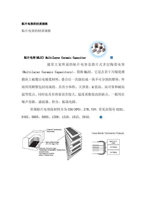
贴片电容的材质规格贴片电容的材质规格贴片电容(MLCC)Multilayer Ceramic Capacitor常规贴片电容按材料分为COG(NPO)、X7R、Y5V,常见封装有0201、0402、0603、0805、1206、1210、1812、2010。
NPO、X7R、Z5U和Y5V的主要区别是它们的填充介质不同。
在相同的体积下由于填充介质不同所组成的电容器的容量就不同,随之带来的电容器的介质损耗、容量稳定性等也就不同。
所以在使用电容器时应根据电容器在电路中作用不同来选用不同的电容器。
上表可看出各个不同材料的温度特性一 NPO电容器NPO是一种最常用的具有温度补偿特性的单片陶瓷电容器。
它的填充介质是由铷、钐和一些其它稀有氧化物组成的。
NPO电容器是电容量和介质损耗最稳定的电容器之一。
在温度从-55℃到+125℃时容量变化为0±30ppm/℃,电容量随频率的变化小于±0.3ΔC。
NPO电容的漂移或滞后小于±0.05%,相对大于±2%的薄膜电容来说是可以忽略不计的。
其典型的容量相对使用寿命的变化小于±0.1%。
NPO电容器随封装形式不同其电容量和介质损耗随频率变化的特性也不同,大封装尺寸的要比小封装尺寸的频率特性好。
NPO电容器适合用于振荡器、谐振器的槽路电容,以及高频电路中的耦合电容。
二 X7R电容器X7R电容器被称为温度稳定型的陶瓷电容器。
当温度在-55℃到+125℃时其容量变化为15%,需要注意的是此时电容器容量变化是非线性的。
X7R电容器的容量在不同的电压和频率条件下是不同的,它也随时间的变化而变化,大约每10年变化1%ΔC,表现为10年变化了约5%。
X7R电容器主要应用于要求不高的工业应用,而且当电压变化时其容量变化是可以接受的条件下。
它的主要特点是在相同的体积下电容量可以做的比较大。
三 Z5U电容器Z5U电容器称为”通用”陶瓷单片电容器。
三星电容规格书
■INTRODUCTIONMLCC(Multilayer Ceramic Capacitor)is SMD(Surface Mounted Device)type capacitor that is used in wide ranges of capacitance.MLCC is paid more attentions than other capacitors due to the better frequency characteristics,higher reliability,higher withstanding voltage and so on.MLCC is made of many layers of ceramic and inner electrodes like sandwich.Pd was used for inner electrodes.But the price of Pd was skyrocketed and Pd was replaced by the BME(Base Metal Electrode),which reduced the total cost of MLCC.This inner electrode is connected to outer termination for surface mounting,which is composed of three layers,Cu or Ag layer,Ni plating layer,and SnPb or Sn plating layer.Most of MLCCs become Pb free by the environmental issue at present.MLCC is divided into two classes.Class I(C0G,etc)is the temperature compensating type.It hasa small TCC(Temperature Coefficient of Capacitance)and a better frequency performance.Therefore,it is used in RF applications such as cellular phone,tuner,and so on.Class II(X7R, X5R,Y5V,etc)is the high dielectric constant type,which is used in general electronic circuit.Especially high capacitance MLCC is replacing other capacitors(Tantalum and Aluminum capacitor)due to the low ESR(Equivalent Series Resistance)value.■FEATURE AND APPLICATION●Feature-Miniature Size-Wide Capacitance and Voltage Range-Highly Reliable Performance-Tape&Reel for Surface Mount Assembly-Low ESR-High Q at High Frequencies-Stable Temperature Dependence of Capacitance●Application-High Frequency Circuit(Tuner,VCO,PAM etc)-General Power Supply Circuit(SMPS etc)-DC-DC Converter-General Electronic Circuit■STRUCTURE■APPEARANCE AND DIMENSIONDIMENSION(mm)CODE EIA CODEL W T(MAX)BW 0302010.6±0.030.3±0.030.3±0.030.15±0.05050402 1.0±0.050.5±0.050.5±0.050.2+0.15/-0.1 100603 1.6±0.10.8±0.10.8±0.10.3±0.2210805 2.0±0.1 1.25±0.1 1.25±0.10.5+0.2/-0.3 311206 3.2±0.2 1.6±0.2 1.6±0.20.5+0.2/-0.3 321210 3.2±0.3 2.5±0.2 2.5±0.20.6±0.3431812 4.5±0.4 3.2±0.3 3.2±0.30.8±0.3552220 5.7±0.4 5.0±0.4 3.2±0.3 1.0±0.3■PREVIOUS PART NUMBERINGSymbol EIA Code TemperatureCoefficient(PPM/℃)※TemperatureCharacteristicsOperationTemperature RangeC C0G(CH)0±30C Δ-55~+125℃P P2H -150±60P ΔR R2H -220±60R ΔS S2H -330±60S ΔT T2H -470±60T ΔU U2J -750±120U ΔLS2L+350~-1000SL▶CLASS Ⅰ(Temperature Compensation)TemperatureCharacteristicsbelow 2.0pF 2.2~3.9pF above 4.0pFabove 10pFC ΔC0G C0G C0G C0G P Δ-P2J P2H P2H R Δ-R2J R2H R2H S Δ-S2J S2HS2H T Δ-T2J T2H T2H U Δ-U2JU2JU2JSymbol EIA Code Capacitance Change(ΔC :%)OperationTemperature RangeA X5R ±15-55~+85℃B X7R ±15-55~+125℃FY5V+22~-82-30~+85℃▶CLASS Ⅱ(High Dielectric Constant)SAMSUNG Multilayer Ceramic Capacitor Type(Size)Capacitance Temperature Characteristics Nominal Capacitance Capacitance Tolerance Rated Voltage Thickness Option Packaging Type CAPACITANCE TEMPERATURE CHARACTERISTICS ※Temperature Characteristics ☞K :±250PPM/℃J :±120PPM/℃H :±60PPM/℃G :±30PPM/℃●●●●●●●●●Temperature CharacteristicsSymbol Tolerance Applicable Capacitance &RangeC0G(NPO)or T.C SeriesB ±0.1pF 0.5~3pF C±0.25pF 0.5~10pF D ±0.5pF F ±1pF 6~10pFG ±2%E-24Series for over 10pF J ±5%K±10%A(X5R)B(X7R)J ±5%E-12SeriesK ±10%M ±20%F(Y5V)Z-20%~+80%E-6Series CAPACITANCE TOLERANCE The nominal capacitance value is expressed in pico-Farad(pF)and identified by three-digit number,first two digits represent significant figures and last digit specifies the number of zeros to follow.For values below 1pF,the letter "R"is used as the decimal point and the last digit becomes significant.example)100:10×10o =10pF 102:10×102=1000pF020:2×10o =2pF1R5:1.5pFNOMINAL CAPACITANCE ●●※Please consult us for special tolerances.RATED VOLTAGE ●PACKAGING TYPE THICKNESS OPTION Symbol Description of the CodeN Standard thickness (please refer to standard thickness table on next page)A Thinner than standard thickness B Thicker than standard thicknessC Standard Thickness High Q (Low `D.F `)D Sn-100%(High-Q)ESn-100%(General)※Please Consult us for other termination type.●●Series Capacitance StepE-3 1.02.24.7E-6 1.01.52.23.34.76.8E-12 1.0 1.2 1.5 1.8 2.2 2.7 3.3 3.9 4.7 5.6 6.88.2E-241.0 1.2 1.5 1.82.2 2.73.3 3.94.75.66.88.21.11.31.62.02.43.03.64.35.16.27.59.1※Standard Capacitance is "Each step ×10n "▶STANDARD CAPACITANCE STEP■NEW PART NUMBERING●PRODUCT ABBREVIATION Symbol Product AbbreviationCLSAMSUNG Multilayer Ceramic Capacitor●SIZE(mm)Symbol Size(mm)Length Width 030.60.305 1.00.510 1.60.821 2.0 1.231 3.2 1.632 3.2 2.543 4.5 3.2555.75.0SAMSUNG Multilayer Ceramic Capacitor Size(mm)Capacitance Temperature Characteristic Nominal Capacitance Capacitance Tolerance Rated Voltage Thickness Option Product &Plating Method Samsung Control Code Reserved For Future Use Packaging Type ●●●●●●●●●●●●CAPACITANCE TEMPERATURE CHARACTERISTICSymbol Temperature Characteristics Temperature RangeCClassⅠCOG C△0±30(ppm/℃)-55~+125℃P P2H P△-150±60R R2H R△-220±60S S2H S△-330±60T T2H T△-470±60U U2J U△-750±60L S2L S△+350~-1000AClassⅡX5R X5R±15%-55~+85℃B X7R X7R±15%-55~+125℃F Y5V Y5V+22~-82%-30~+85℃※Temperature CharacteristicTemperatureCharacteristicsBelow2.0pF 2.2~3.9pF Above4.0pF Above10pF CΔC0G C0G C0G C0GPΔ-P2J P2H P2HRΔ-R2J R2H R2HSΔ-S2J S2H S2HTΔ-T2J T2H T2HUΔ-U2J U2J U2JJ:±120PPM/℃,H:±60PPM/℃,G:±30PPM/℃●NOMINAL CAPACITANCENominal capacitance is identified by3digits.The first and second digits identify the first and second significant figures of the capacitance. The third digit identifies the multiplier.'R'identifies a decimal point.●ExampleSymbol Nominal Capacitance1R5 1.5pF10310,000pF,10nF,0.01μF104100,000pF,100nF,0.1μF●CAPACITANCE TOLERANCE Symbol Tolerance Nominal CapacitanceA ±0.05pF Less than 10pF (Including 10pF)B ±0.1pFC ±0.25pFD ±0.5pF F ±1pF F ±1%More than 10pF G ±2%J ±5%K ±10%M ±20%Z+80,-20%●RATEDVOLTAGE●THICKNESS OPTIONType Symbol Thickness(T)Spec 060330.30±0.03 100550.50±0.05 160880.80±0.102012A0.65±0.10 C0.85F 1.25±0.103216C0.85±0.15 F 1.25±0.15 H 1.6±0.203225F 1.25±0.20H 1.6I 2.0J 2.54532F 1.25±0.20H 1.6I 2.0J 2.5L 3.2±0.305750F 1.25±0.20H 1.6I 2.0J 2.5L 3.2±0.30●PRODUCT&PLATING METHODSymbol Electrode Termination Plating TypeA Pd Ag Sn_100%N Ni Cu Sn_100%G Cu Cu Sn_100%●SAMSUNG CONTROL CODE●RESERVED FOR FUTURE USESymbol Description of the codeN Reserved for future use●PACKAGING TYPE▶CAPACITANCE vs CHIP THICKNESS STANDARDDescription0603(0201)1005(0402)1608(0603)2012Type (0805)3216Type (1206)3225Type (1210)4532Type (1812)5750Type (2220)Dimension (mm)L0.6±0.03 1.0±0.05 1.6±0.1 2.0±0.13.2±0.153.2±0.2 3.2±0.34.5±0.45.7±0.4W 0.3±0.030.5±0.050.8±0.1 1.25±0.1 1.6±0.15 1.6±0.22.5±0.23.2±0.3 5.0±0.4T0.3±0.030.5~±0.050.8±0.10.65±0.10.85±0.11.25±0.10.85±0.15 1.25±0.15 1.6±0.21.25±0.2 1.6±0.22.0±0.22.5±0.21.25±0.21.6±0.22.0±0.22.5±0.21.6±0.22.0±0.22.5±0.2C A P ACIT A N CER A N G E (p F )SL 50V -0.5~2400.5~10000.5~10001100~15001600~27000.5~27003000~56006200~8200-----------C,TC (Except SL,UJ)25V 0.5~470.5~2200.5~1000--3300~82001500~36003900~68007500~10000-----100000-----50V -0.5~1800.5~10000.5~560620~10001100~33000.5~22002400~4700-560~1000011000~2200024000~47000-1000~1300015000~2200024000~4700062000~680004300093000130000C A P A C I T A N C E R A N G E (n F )A (X5R)6.3V 102202200--10000--10000---22000---47000--4700010V101001000--2200--4700~10000---22000------4700016V -47330~470--1000--4700---6800~10000-------25V --------------------50V- 6.8~10------------------B (X7R)6.3V 0.1~1047~100470~1000--1000--6800~10000---22000-------10V0.1~1033~100220~470220~270330~470560~1000-1000~330047001500~220033003900~4700----22000---16V0.1~110~33100~22068~200220~330390~1000330~6801000~15002200~33001500~220033003900~4700---2200----25V -4.7~1047~10039~6882~100150~470100~330470~620680~1000680~150018002200---1000---1000050V -0.22~4.70.22~1000.22~3947~1002201~150220390~1000 2.2~680820~1000--10~1000-----3300~4700F (Y5V)6.3V10~100-2200--10000-----47000--------10V -220~330100~1000--4700-470010000~22000---22000------10000016V -10~220100~100010~680820~10001200~22001000~22002700~4700100003300~68001000015000---22000----25V -10~3322~33010~220270~470560~1000470~10001200~22002700~33001000~33004700~10000-----10000---50V - 2.2~102.2~1002.2~6882~150180~100010~470560~1000-100~1000------10000---■PACKAGING●CARDBOARD PAPER TAPESymbol W F E P1P2P0D tABTypeD i m e n s i o n038.0±0.3 3.5±0.05 1.75±0.12.0±0.052.0±0.05 4.0±0.1Φ1.5+0.1/-00.37±0.030.38±0.030.68±0.03050.6±0.050.65+0.05/-0.1 1.15+0.05/-0.110 4.0±0.11.1MAX1.1±0.21.9±0.221 1.6±0.22.4±0.2312.0±0.23.6±0.2unit :mm●EMBOSSED PLASTIC TAPE●TAPING SIZE●REEL DIMENSIONSymbol A B CDEWtR7"Reel φ178±2.0min.φ50φ13±0.521±0.82.0±0.510±1.50.8±0.21.013"Reelφ330±2.0min.φ70unit :mmSymbol Cardboard Paper TapeEmbossed Plastic Tape7"Reel 4000200013"Reel15000-unit :pcsSize 05(0402)10(0603)21(0805)T ≤0.85mm T ≥1.0mm Quantity 50,00010,000~15,000*10,0005,000●BULK CASE PACKAGING-Bulk case packaging can reduce the stock space and transportation costs.-The bulk feeding system can increase the productivity.-It can eliminate the componentsloss.Symbol A B T C D E Dimension 6.8±0.18.8±0.112±0.1 1.5+0.1/-02+0/-0.14.7±0.1Symbol F W G H L I Dimension31.5+0.2/-036+0/-0.219±0.357±0.35110±0.75±0.35●QUANTITY*Option■CHARACTERISTIC MAP●CLASSⅠTemperature Characteristics Size VoltageCapacitance Range(㎊)SL,UJ05 (0402)50V10 (0603)50V21 (0805)50V31 (1206)50VC(COG)& TC Series03(0201)25V05(0402)25V50V10(0603)25V50V21(0805)25V50V31(1206)25V50V 32(1210)50V100V43(1812)25V50V55(2220)50V101001000100001000001000000100000001000000000.5240270082001000100010000150033004700100018022047820033001800047005604700068000100010000013000043000●CLASSⅡ,A(X5R)Temperature Characteristics Size Voltage Capacitance Range(㎊)A(X5R)0603(0201)6.3V10V1005(0402)6.3V10V16V50V1608(0603)6.3V10V16V2012(0805)6.3V10V16V3216(1206)6.3V10V16V3225(1210)6.3V10V16V4532(1812) 6.3V5750(2220)6.3V10V101001000100001000001000000100000001000000001000010000010000100000004700000220000002200000100000004700000220000004700000047000100006800100000022000001000000470000330000100000001000000068000004700000047000000220000●CLASSⅡ,B(X7R)Temperature Characteristics Size VoltageCapacitance Range(㎊)B(X7R)03(0201)6.3V10V16V05(0402)6.3V10V16V25V50V10(0603)6.3V10V16V25V50V21(0805)6.3V10V16V25V50V31(1206)6.3V10V16V 25V50V10100100010000100000100000010000000100000000100000470004700000470000100000100000047000022000010000003300000100000010000001001000010000000100000100000100100001001000680000033000100003300010000470047002204700002200002200001000004700022022000010000006800039000220100000033000010000010000001000●CLASSⅡ,B(X7R)Temperature Characteristics Size VoltageCapacitance Range(㎊)B(X7R)32(1210)6.3V10V16V25V50V43(1812)10V16V25V50V55(2220)25V50V1010010001000010000010000001000000010000000022000000100000010000470000015000002200000010000001000000047000003300000470000015000002200000680000100000022002200000●CLASSⅡ,F(Y5V)Temperature Characteristics Size VoltageCapacitance Range(㎊)F(Y5V)03(0201) 6.3V05(0402)10V16V25V50V10(0603)6.3V10V16V25V50V21(0805)6.3V10V16V25V50V31(1206)10V16V 25V50V32(1210)6.3V10V16V25V50V43(1812)16V25V50V55(2220)10V330000330001000022000010000220010000003300001000001000002200022001000000220000010000100002200000047000001000000033000001000000100000047000010000470000010000001500000033000001000000100000100000002200000010000220000100000001000000010000000022000001000000010000010000100000010000010000002200470000002200000010100100010000100000100000010000000100000000■RELIABILITY TEST DATANO ITEM PERFORMANCE TEST CONDITION 1APPEARANCE NO ABNORMAL EXTERIOR APPEARANCE THROUGH MICROSCOPE(×10)2INSULATIONRESISTANCE10,000㏁OR500㏁·㎌PRODUCT WHICHEVER ISSMALLER(RATED VOLTAGE IS BELOW16V:10,000㏁OR100㏁·㎌)RATED VOLTAGE SHALL BE APPLIED.MEASUREMENT TIME IS60~120RATED VOLTAGETIME60SEC.3WITHSTANDINGVOLTAGENO DIELECTRIC BREAKDOWN ORMECHANICAL BREAKDOWNCLASSⅠ:300%OF THE RATED VOLTAGE FOR1~5SEC,CLASSⅡ:250%OF THE RATED VOLTAGE FOR1~5SECIS APPLIED WITH LESS THAN50㎃CURRENT4CAPACITANCECLASSⅠWITHIN THE SPECIFIEDTOLERANCECAPACITANCE FREQUENCY VOLTAGE1,000㎊ANDBELOW1㎒±10%0.5~5VrmsMORE THAN1,000㎊1㎑±10%CLASSⅡWITHIN THE SPECIFIEDTOLERANCECAPACITANCE FREQUENCY VOLTAGE10㎌AND BELOW1㎑±10% 1.0±0.2VrmsMORE THAN10㎌120㎐±20%0.5±0.1Vrms5Q CLASSⅠOVER30㎊:Q≥1,000LESS THAN30㎊:Q≥400+20C(C:CAPACITANCE)CAPACITANCE FREQUENCY VOLTAGE1,000㎊ANDBELOW1㎒±10%0.5~5VrmsMORE THAN1,000㎊1㎑±10%6TanδCLASSⅡ1.CHAR:B2.CHAR:FCAPACITANCE FREQUENCY VOLTAGE10㎌AND BELOW1㎑±10% 1.0±0.2VrmsMORE THAN10㎌120㎐±20%0.5±0.1Vrms RATED VOLTAGE DF SPEC6.3V0.05max10V0.05max16V0.035max25V0.025max50V이상0.025max6.3V10V16V25V50V1005-0.125max0.09max(C<220nF)0.125max(C≥220nF)0.05max0.05max16080.16max0.125max0.09max0.05max(C≤100nF)0.07max(C>100nF)0.05max20120.16max0.125max0.09max0.07max0.05max32160.16max0.125max0.09max0.07max0.05max32250.16max0.125max0.09max0.07max(C≤6.8㎌)0.09max(C>6.8㎌)0.05max45320.16max0.16max0.09max--57500.125max---www.cdindustries.hk*THE INITIAL VALUE OF HIGH DIELECTRIC CONSTANT SERIES SHALL BE MEASUREDAFTER THE HEAT TREATMENT OF150+0/-10℃,1Hr AND SITTING OF48±4hr AT ROOM TEMPERATURE&ROOM HUMIDITY.NO ITEM PERFORMANCE TEST CONDITION14HUMIDITY(STEADYSTATE)APPEARANCE NO MECHANICAL DAMAGE SHALL OCCUR TEMPERATURE:40±2℃RELATIVE HUMIDITY:90~95%RHTEST TIME:500+12/-0Hr.MEASURE AT ROOM TEMPERATUREAFTER COOLING FORCLASSⅠ:24±2Hr.CLASSⅡ:48±4Hr.CAPACITANCECHARACTERISTIC CAPACITANCE CHANGECLASSⅠWITHIN±5%OR±0.5㎊WHICHEVERIS LARGERCLASSⅡA,B WITHIN±12.5%F WITHIN±30%QCLASSⅠ30㎊AND OVER:Q≥35010~30㎊:Q≥275+2.5×CLESS THAN10pF:Q≥200+10×CTanδCLASSⅡINSULATIONRESISTANCEMINIMUM INSULATION RESISTANCE:1,000㏁OR50㏁·㎌PRODUCT WHICHEVER ISSMALLER15MOISTURERESISTANCEAPPEARANCE NO MECHANICAL DAMAGE SHALL OCCUR APPLIED VOLTAGE:RATED VOLTAGETEMPERATURE:40±2℃RELATIVE HUMIDITY:90~95%RHTEST TIME:500+12/-0Hr.CURRENT APPLIED:50㎃MAX.<INITIAL MEASUREMENT>CLASSⅡSHOULD BE MEASUREDINITIAL VALUE AFTER BE HEAT-TREATEDFOR1HR IN150℃+0/-10℃AND BE LEFTFOR48±4HR AT ROOM TEMPERATURE.<LATTER MEASUREMENT>CLASSⅠSHOULD BE MEASURED AFTERLEFT FOR24±2HRS IN ROOMTEMPERATURE AND HUMIDITY.CLASSⅡSHOULD BE MEASUREDLATTER VALUE AFTER BEHEAT-TREATED FOR1HR IN150℃+0/-10℃AND BE LEFT FOR48±4HR AT ROOMTEMPERATURE.CAPACITANCECHARACTERISTIC CAPACITANCE CHANGECLASSⅠWITHIN±7.5%OR±0.75㎊WHICHEVERIS LARGERCLASSⅡA,B WITHIN±12.5%FWITHIN±30%WITHIN+30~-40%1005C>0.47μF1608C>1.0μF2012C>4.7μF3216C>10.0μF3225C>22.0μF4532C>47.0μFQCLASSⅠ30㎊AND OVER:Q≥20030㎊AND BELOW:Q≥100+10/3×CTanδCLASSⅡINSULATIONRESISTANCEMINIMUM INSULATION RESISTANCE:500㏁OR25㏁·㎌PRODUCT,WHICHEVER IS SMALLER.CHAR.25VANDOVER16V10V 6.3V4VA,B0.050.05MAX0.05MAX0.075MAX0.1MAXF0.075MAX0.1MAX(C〈1.0㎌)0.125MAX(C≥1.0㎌)0.15MAX0.195MAX0.25MAXCHAR.25VANDOVER16V10V 6.3V4VA,B0.05MAX0.05MAX0.05MAX0.075MAX0.1MAXF0.075MAX0.1MAX(C〈1.0㎌)0.125MAX(C≥1.0㎌)0.15MAX0.195MAX0.25MAX6.3VTanδ0.125MAX*ConditionCLASSⅡ(A,B)1005C≥0.22㎌1608C≥2.2㎌2012C≥4.7㎌3216C≥10.0㎌3225C≥22.0㎌4532C≥47.0㎌5750C≥100.0㎌6.3V Tanδ0.125MAX*ConditionCLASSⅡ(A,B)1005C≥0.22㎌1608C≥2.2㎌2012C≥4.7㎌3216C≥10.0㎌3225C≥22.0㎌4532C≥47.0㎌5750C≥100.0㎌NO ITEM PERFORMANCE TEST CONDITION16HIGHTEMPERATURERESISTANCEAPPEARANCE NO MECHANICAL DAMAGE SHALL OCCURAPPLIED VOLTAGE:150%,200%OF RATED VOLTAGETEST TIME:1000+48/-0Hr.CURRENT APPLIED:50㎃MAX.<INITIAL MEASUREMENT>CLASSⅡSHOULD BE MEASURED INITIALVALUE AFTER BE HEAT-TREATED FOR1HR IN150℃+0/-10℃AND BE LEFT FOR48±4HR AT ROOM TEMPERATURE.<LATTER MEASUREMENT>CLASSⅠSHOULD BE MEASURED AFTERLEFT FOR24±2HRS IN ROOMTEMPERATURE AND HUMIDITY.CLASSⅡSHOULD BE MEASURED LATTERVALUE AFTER BE HEAT-TREATED FOR1HR IN150℃+0/-10℃AND BE LEFT FOR48±4HR AT ROOM TEMPERATURE.(TWICE OF RATED VOLTAGE WILL BEAPPLIED TO ALL SERIES BUT ABOVE)**HOWEVER,A/B는1005C≥0.22㎌SEE(FIG.3)CAPACITANCECHARACTERISTIC CAP.CHANGECLASSⅠWITHIN±3%OR±0.3㎊,WHICHEVER IS LARGERCLASSⅡA,B WITHIN±12.5%FWITHIN±30%WITHIN+30~40%1005C>0.47μF1608C>1.0μF2012C>4.7μF3216C>10.0μF3225C>22.0μF4532C>47.0μFQCLASSⅠ30㎊AND OVER:Q≥35010~30㎊:Q≥275+2.5×CLESS THAN10㎊:Q≥200+10×CTanδCLASSⅡINSULATIONRESISTANCEMINIMUM INSULATION RESISTANCE:1,000㏁OR50㏁·㎌PRODUCTWHICHEVER IS SMALLER17TEMPERATURECYCLEAPPEARANCE NO MECHANICAL DAMAGE SHALL OCCUR CAPACITORS SHALL BE SUBJECTEDTO FIVE CYCLES OF THETEMPERATURE CYCLE AS FOLLOWINGSTEP TEMP.(℃)TIME(MIN)1MIN.RATEDTEMP.+0/-3302252~33MAX.RATEDTEMP.+3/-0304252~3MEASURE AT ROOM TEMPERATUREAFTER COOLING FORCLASSⅠ:24±2Hr.CLASSⅡ:48±4Hr.CAPACITANCECHARACTERISTIC CAP.CHANGECLASSⅠWITHIN±2.5%OR±0.25㎊WHICHEVER ISLARGERCLASSⅡA,B WITHIN±7.5%F WITHIN±20%QCLASSⅠ30㎊AND OVER:Q≥1000LESS THAN30㎊:Q≥400+20×CTanδCLASSⅡTO SATISFY THE SPECIFIEDINITIAL VALUEINSULATIONRESISTANCETO SATISFY THE SPECIFIEDINITIAL VALUECHAR.25VANDOVER16V10V 6.3V4VA,B0.05MAX0.05MAX0.05MAX0.075MAX0.1MAXF0.075MAX0.1MAX(C<1.0㎌)0.125MAX(C≥1.0㎌)0.15MAX0.195MAX0.25MAXCHAR.TEMP.CLASSⅠ125±3℃CLASSⅡA85±3℃B125±3℃F85±3℃*150%Authorization ConditionsCLASSⅡ(A,B,F)1005C>0.47μF1608C≥2.2㎌2012C≥4.7㎌3216C≥10.0㎌3225C≥22.0㎌4532C≥47.0㎌5750C≥100.0㎌■CHARACTERISTIC GRAPH▶CAPACITANCE CHANGE -AGING▶CAPACITANCE -DC VOLTAGE CHARACTERISTICS▶CAPACITANCE -TEMPERATURE CHARACTERISTICS●ELECTRICAL CHARACTERISTICS■APPLICATION MANUAL●Storage Condition▶Storage EnvironmentThe electrical characteristics of MLCCs were degraded by the environment of high temperature or humidity.Therefore,the MLCCs shall be stored in the ambient temperature and the relative humidity of less than40℃and70%,respectively.Guaranteed storage period is within6months from the outgoing date of delivery.▶Corrosive GasesSince the solderability of the end termination in MLCC was degraded by a chemical atmosphere such as chlorine,acid or sulfide gases,MLCCs must be avoid from these gases.▶Temperature FluctuationsSince dew condensation may occur by the differences in temperature when the MLCCs are taken out of storage,it is important to maintain the temperature-controlled environment.●Design of Land PatternWhen designing printed circuit boards,the shape and size of the lands must allow for theproper amount of solder on the capacitor.The amount of solder at the end terminations has a direct effect on the crack.The crack in MLCC will be easily occurred by the tensile stress which was due to too much amount of solder.In contrast,if too little solder is applied,the termination strength will be e the following illustrations as guidelines for proper land design.Recommendation of Land Shape and Size●AdhesivesWhen flow soldering the MLCCs,apply the adhesive in accordance with the following conditions.▶Requirements for AdhesivesThey must have enough adhesion,so that,the chips will not fall off or move during thehandling of the circuit board.They must maintain their adhesive strength when exposed to soldering temperature.They should not spread or run when applied to the circuit board.They should harden quickly.They should not corrode the circuit board or chip material.They should be a good insulator.They should be non-toxic,and not produce harmful gases,nor be harmful when touched.▶Application MethodIt is important to use the proper amount of adhesive.Too little and much adhesive will cause poor adhesion and overflow into the land,respectively.▶Adhesive hardening CharacteristicsTo prevent oxidation of the terminations,the adhesive must harden at160℃or less,within2minutes or less.●Mounting▶Mounting Head PressureExcessive pressure will cause crack to MLCCs.The pressure of nozzle will be300g maximum during mounting.▶Bending StressWhen double-sided circuit boards are used,MLCCs first are mounted and soldered onto one side of the board.When the MLCCs are mounted onto the other side,it is important to support the board as shown in the illustration.If the circuit board is not supported,the crack occur to the ready-installed MLCCs by the bending stress.●FluxAlthough the solderability increased by the highly-activated flux,increase of activity in flux may also degrade the insulation of the chip capacitors.To avoid such degradation,it is recommended that a mildly activated rosin flux(less than0.2%chlorine)be used.●SolderingSince a multilayer ceramic chip capacitor comes into direct contact with melted solder during soldering,it is exposed to potentially mechanical stress caused by the sudden temperature change.The capacitor may also be subject to silver migration,and to contamination by the flux.Because of these factors,soldering technique is critical.▶Soldering MethodsMethodClassificationReflow soldering-Overall heating-Infrared rays -Hot plate-VPS(vapor phase)-Local heating-Air heater -Laser-Light beamFlow soldering-Single wave -Double wave-*We recommend the reflow soldering method.▶Soldering ProfileTo avoid crack problem by sudden temperature change,follow the temperature profile in the adjacentgraph.30025020015010050℃Reflow Soldering 30025020015010050℃60~120sec 3~4secFlow Soldering▶Manual SolderingManual soldering can pose a great risk of creating thermal cracks in chip capacitors.The hotsoldering iron tip comes into direct contact with the end terminations,and operator's carelessnessmay cause the tip of the soldering iron to come into direct contact with the ceramic body of the capacitor.Therefore the soldering iron must be handled carefully,and close attention must be paid to the selection of the soldering iron tip and to temperature control of the tip.▶Amount ofSolder▶CoolingNatural cooling using air is recommended.If the chips are dipped into solvent for cleaning, the temperature difference(△T)must be less than100℃6-6.CleaningIf rosin flux is used,cleaning usually is unnecessary.When strongly activated flux is used, chlorine in the flux may dissolve into some types of cleaning fluids,thereby affecting the chip capacitors.This means that the cleaning fluid must be carefully selected,and should always be new.▶Notes for Separating Multiple,Shared PC Boards.A multi-PC board is separated into many individual circuit boards after soldering has been completed.If the board is bent or distorted at the time of separation,cracks may occur in the chip capacitors.Carefully choose a separation method that minimizes the bending of the circuit board.■CROSS REFERENCEP/N COMPANY SAMSUNG AVX JOHANSON KEMET KYOCERA MURATA NOVACAP PANASONIC ROHMTAIYO-YUDENTDK VITRAMON①COMPANY MODEL(MLCC)CL--C CM GRM-ECJ MCH MK C VJ②SIZE (EIA/JIS)0201(0603)03---0333-Z-0630603-0402(1005)050402R0704020536040201510510050402 0603(1608)100603R14060310539060311810716080603 0805(2012)210805R1508052140080522121220120805 1206(3216)311206R181********-6120633131632161206 1210(3225)321210S4112103242-2121043232532251210 1808(4520)421808R29180842-1808---45201808 1812(4532)431812S4318124343-21812-4343245321812 2220(5750)55--22205544-12221--5505650-③TEMPERATURE CHARACTERISTIC COG(NPO)C A N G CG COG/CH N C A C COG/CH A P2H(N150)P S--P P2H-P-P PH-R2H(N220)R1--R R2H-R-R RH-S2H(N330)S3--S S2H-S-S SH-T2H(N470)T O--T T2H-T-T TH-U2J(N750)U Z--U U2J-U UJ U UJ-S2L L Y--SL SL-G SL SL SL-X7R B C W R(X)X7R X7R B B C BJ X7R(B)Y(X) Z5U E E Z U-Z5U Z-E-Z5U U Y5V F G Y V Y5V Y5V Y F F F Y5V-④NOMINAL CAPACITANCE EX)103=10,000㎊221=220㎊225=2,200,000㎊=2.2㎌1R5=1.5㎊010=1㎊⑤CAPACITANCE TOLERANCE B:±0.1㎊C:±0.25㎊D:±0.5㎊F:±1%G:±2%J:±5%K:±10%M:±20%Z:-20~+80%⑥RATED VOLTAGE6.3V Q6-906 6.3-0J-J0J-10V P Z10081010-1A4L1A-16V O Y160416161601C3E1C J 25V A3250325252501E2T1E X 50V B5500550505001H5U1H A 100V C110111*********A1-2A B 200V D220122002002012D---C 250V E V--250250251---2E-500V G7501-500500501----E 630V H---630630----2J-1000V I A102-10001K102---3A G 2000V J G202-20002K202---3D-3000V K H302-30003K302---3F H 4000V-J-4000-402-----⑦TERMINATIONNICKEL BARRIER N T V C A(GRM)N-(MCH)--X Ag/Pd P1--B(GR)P-(MC)--F⑧PACKAGEBULK(VINYL)B9(NONE)-B PB*X-B B B PAPER TAPING C2,4T,R-T,L PT T E,V,W K,L T T C,P PLASTIC TAPING E1,3E,U-H,N PT-F,Y P,Q T-T,R BULK CASE P7--C PC-C C--G。
三星电容规格书

三星电容规格书1. 引言本规格书旨在介绍三星电容的详细规格和特性。
三星电容是一种高质量、可靠性强的电子元件,广泛应用于各种电路和设备中。
本文将从技术参数、材料特性、封装形式以及应用领域等方面对三星电容进行全面介绍。
2. 技术参数2.1 电容值三星电容提供多种不同的电容值,范围从几皮法到数百微法。
具体的电容值取决于产品型号和系列。
2.2 额定电压每个三星电容都有一个额定电压,表示其能够承受的最大工作电压。
额定电压可以从几伏到数百伏不等。
2.3 容差三星电容的容差指标表明了其实际值与标称值之间的允许偏差范围。
常见的容差包括±5%、±10%等。
2.4 工作温度范围三星电容适用于不同的工作温度范围,常见的工作温度范围包括-40℃至+85℃、-55℃至+125℃等。
2.5 极性部分三星电容是极性电容,需要按照正确的极性连接。
而非极性电容则不受极性限制。
3. 材料特性3.1 介质材料三星电容的介质材料通常采用高质量的聚合物或陶瓷材料。
这些材料具有良好的绝缘性能和稳定性,以确保电容的长期可靠运行。
3.2 极板材料三星电容的极板通常采用优质金属,如铝或钽。
这些金属具有良好的导电性和耐腐蚀性,以确保电容在工作中能够提供稳定可靠的电流传输。
3.3 封装材料三星电容的封装材料通常采用环保型塑料或金属外壳。
这些封装材料具有良好的机械强度和耐高温特性,以保护内部元件并提供稳定的外部连接。
4. 封装形式4.1 表面贴装型(SMD)三星电容可提供表面贴装型封装,方便在PCB上进行自动化焊接。
常见的封装形式有0805、1206、1210等,具体尺寸取决于电容的电容值和额定电压。
4.2 插件型三星电容也可提供插件型封装,适用于手工焊接或特殊应用场景。
插件型封装通常具有引脚,可直接插入PCB或插座中。
5. 应用领域5.1 通信设备三星电容广泛应用于各种通信设备,如手机、无线路由器、基站等。
其高质量和稳定性能确保了通信设备的可靠运行和优秀的信号传输质量。
39uf 电解电容规格书
39uf 电解电容规格书规格书编号:DC-2022-001日期:2022年10月1日1. 引言本规格书旨在描述39uf电解电容器的主要规格和性能指标,以供客户参考和选择使用。
在阅读本规格书前,请确保您对39uf电解电容器的基本知识有一定了解。
2. 产品描述2.1 产品名称:39uf 电解电容器2.2 产品型号:C39UF20222.3 产品封装:铝电解电容器(电解质为铝酸盐)2.4 产品外形尺寸:直径14mm,高度25mm2.5 产品工作温度范围:-40℃至+105℃2.6 产品电压额定值:50V2.7 产品容量:39微法(±20%容差)3. 性能指标3.1 直流电阻(ESR):不超过10欧姆3.2 漏电流:不超过0.02CV或3毫安(取较大值)3.3 最大涟漪电流:30毫安有效值3.4 寿命:5000小时(温度为105℃,涟漪电流为最大涟漪电流时)3.5 极性:正极带标记,负极为未标记一端3.6 绝缘电阻:1000兆欧姆或者RC×C(μF),以较小值为准(其中RC为产品额定电压)4. 安装与使用建议4.1 安装电解电容器时,请确保极性正确。
否则,可能会导致电容器损坏或电路故障。
4.2 在使用39uf电解电容器时,请尽量避免超过额定电压和温度范围,以延长产品使用寿命。
4.3 当电容器长时间未使用时,请断开其电源并将其储存于低温、低湿度环境中,以保持其性能和寿命。
5. 产品认证与标准5.1 本产品符合国际电工委员会(IEC)的IEC 60384-1标准要求。
5.2 此外,本产品还通过了ISO 9001质量管理体系认证。
6. 包装与交货6.1 39uf电解电容器将被包装在防静电袋中,以防止静电对产品造成损害。
6.2 产品交货将按照双方协商的时间和地点进行。
7. 售后服务7.1 对于质量问题,请在收到产品后的7个工作日内与我们联系,我们将提供免费的维修或更换服务。
7.2 对于非质量问题的退货和更换,需按照公司规定的退换货流程进行。
电容

LED背光源技术凭借其独特、压倒性的优势,逐渐显示出强大的应用前景。那么,今天小Nan就为大家来深入解析一下LED背光技术与CCFL背光技术相比较,LED背光技术到底有哪些优势所在,为何在显示器市场中尤为火爆?
LED背光技术:十大领先优势
LED作为LCD的背光源,与传统背光技术相比,除了在色域范围的优势外,还有很多独特的优点,归纳为十个方面:
贴片电容(MLCC): 日系:TDK(东京电气化学),MURATA(村田),TAIYO YUDEN(太阳诱电),KYOCERA(京瓷) 台系:YAGEO(国巨),WALSIN(华新科)
电感:日本:TDK,MURATA,TAIYO,线艺(美国),这些厂家代表业内最高水平。
中国:顺络,南宏,丰华,麦捷,
LED背光技术优势之二:轻薄雅致
LED背光源则是由众多栅格状的半导体组成,每个“格子”中都拥有一个LED半导体,这样就可以成功实现光源的平面化。其平面化的光源不仅拥有优异的亮度均匀性,还不需要复杂的光路设计。这样一来,LCD的厚度就能做得更加轻薄,同时还能拥有更高的可靠性和稳定性。
4)完美的运动图像。传统CCFL灯管的闪烁发光频率较低,表现动态场景可能产生画面跳动。LED背光可以灵活调整发光频率,而且频率大大高于CCFL,因此能完美地呈现运动画面。
5)实时色彩管理。由于红绿蓝3色独立发光,很容易精确控制目前的显示色彩特性。
6)可以调整的背光白平衡,同时保证整体对比度。当用户的视频源在计算机和DVD机间切换时,可以轻松在9600K和6500K间调整白平衡,而且不会牺牲亮度和对比度。
LED背光技术优势之三:超广色域
LED背光源具有发光更加均匀的特点,在色彩表现力上远胜于CCFL背光源。可对显示色彩数量不足的液晶技术上起到很好的弥补作用,轻松实现NTSC 118%甚至更高的广色域,让液晶显示器真实地还原现五彩缤纷的大自然中的鲜艳色彩。
各种贴片电容容值规格参数表

各种贴片电容容值表X7R贴片电容简述X7R贴片电容属于EIA规定的Class 2类材料的电容。
它的容量相对稳定。
X7R贴片电容特性具有较高的电容量稳定性,在-55℃~125℃工作温度范围内,温度特性为±15%。
层叠独石结构,具有高可靠性。
优良的焊接性和和耐焊性,适用于回流炉和波峰焊。
应用于隔直、耦合、旁路、鉴频等电路中。
X7R贴片电容容量范围厚度与符号对应表符号A C E G J K M N P Q X Y Z最大厚度毫米(英寸)0201~1206 X7R贴片电容选型表封装尺020040060080120125112*********工作电2011125102050100A150A220330AJJJKJCGGJJ470ACGGJJJJJJK680电容(pFGGJJJJJJC1000AK1500CGGJJJJJJJJJJJJM2200GGJJJJJCCJJJJJJ3300JMCGJJJJJJJ4700JJJJJMJ JG J J J J CC P6800 J J J J J JJ J J J J J J G J J J CJ J PC G G J J J J J J J J J J J MC G MJ JJJJ J J J JJ MJ G M 电容量 J J J J J J J J MG G (uF)J J J J M J J J J J MJJJ J J G JJ J PJG G GJ J J J J J J J MJ J J J J J J GG J J M J J J JJ J M M M MN M M M MN M MQ M N MPQ1625501016255010010162550工作电压 1610020010162550100200500 0603080512060201封装尺寸04021210~2225 X7R贴片电容选型表封装尺121181182222222 1125102050510205051051020工作电510 10001500JJJJJJM2200电容(pF3300JJJJJJM4700JJJJJJM6800JJJJJJMKKKKMMXXXXMPJJJJJJPKKKPMMXXXXMPJJJJJJKKKXMMXXXXMPJJJJJJKKKZMMXXXXMPJJJJJMKKKMMXXXXMPJJJJMKKPMMXXXXMP电容(uFMJJZMKMPXXXMJJMMMMZKPMMXXXMPZMMMXZPNNXPNNMMXQZ1010162550工作电压 100200500501002005005010050100200501002225 封装尺寸1825181212102220NPO COG 贴片电容容量规格表默认分类 2009-07-15 16:28 阅读354 评论1字号:大大中中小小NPO贴片电容简述NPO(COG)贴片电容属于Class 1温度补偿型电容。
电容尺寸规格对照表

电容尺寸规格对照表电容器是电子元器件中常见的一种,其作用是存储电荷并在电路中起到滤波、隔离、耦合等作用。
在电子产品的设计和制造中,电容器的尺寸规格是非常重要的参数之一。
本文将按照电容器的类型,为大家介绍电容尺寸规格对照表。
一、电解电容器电解电容器是一种极性电容器,其正负极性必须正确连接。
电解电容器的尺寸规格通常以直径和长度为主要参数。
常见的电解电容器尺寸规格如下:1. 6.3×11mm2. 8×12.5mm3. 10×16mm4. 12.5×20mm5. 16×25mm6. 18×35mm7. 22×40mm8. 25×40mm9. 30×50mm二、陶瓷电容器陶瓷电容器是一种非极性电容器,其尺寸规格通常以直径和厚度为主要参数。
陶瓷电容器的尺寸规格如下:1. 2.5×5mm2. 3.2×6.5mm3. 5×11mm4. 7.5×13mm5. 10×20mm6. 13×25mm7. 16×31mm8. 18×40mm9. 22×45mm三、聚酯薄膜电容器聚酯薄膜电容器是一种非极性电容器,其尺寸规格通常以长度、宽度和厚度为主要参数。
聚酯薄膜电容器的尺寸规格如下:1. 5×11mm2. 7.5×13mm3. 10×20mm4. 13×25mm5. 16×31mm6. 18×40mm7. 22×45mm8. 27×50mm9. 33×60mm四、聚丙烯薄膜电容器聚丙烯薄膜电容器是一种非极性电容器,其尺寸规格通常以长度、宽度和厚度为主要参数。
聚丙烯薄膜电容器的尺寸规格如下:1. 5×11mm2. 7.5×13mm3. 10×20mm4. 13×25mm5. 16×31mm6. 18×40mm7. 22×45mm8. 27×50mm9. 33×60mm总结电容尺寸规格对照表是电子产品设计和制造中必不可少的参考资料。
电容器型号和描述手册说明书
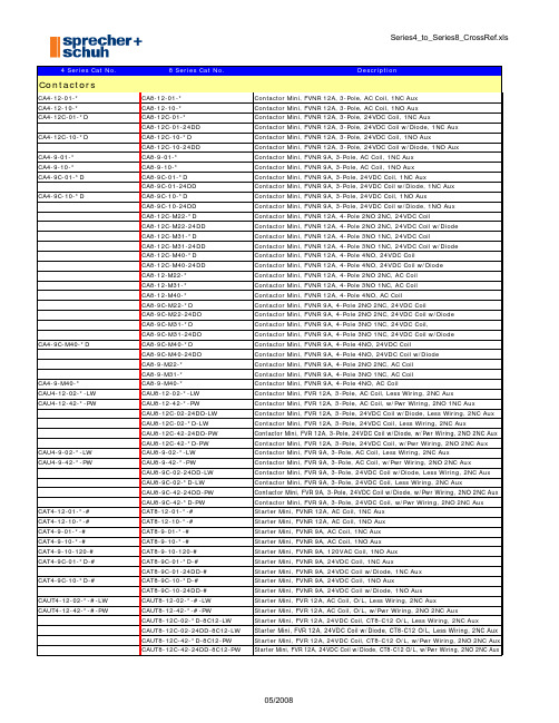
ContactorsCA4-12-01-*CA8-12-01-*Contactor Mini, FVNR 12A, 3-Pole, AC Coil, 1NC AuxCA4-12-10-*CA8-12-10-*Contactor Mini, FVNR 12A, 3-Pole, AC Coil, 1NO AuxCA4-12C-01-*D CA8-12C-01-*Contactor Mini, FVNR 12A, 3-Pole, 24VDC Coil, 1NC AuxCA8-12C-01-24DD Contactor Mini, FVNR 12A, 3-Pole, 24VDC Coil w/Diode, 1NC AuxCA4-12C-10-*D CA8-12C-10-*D Contactor Mini, FVNR 12A, 3-Pole, 24VDC Coil, 1NO AuxCA8-12C-10-24DD Contactor Mini, FVNR 12A, 3-Pole, 24VDC Coil w/Diode, 1NO AuxCA4-9-01-*CA8-9-01-*Contactor Mini, FVNR 9A, 3-Pole, AC Coil, 1NC AuxCA4-9-10-*CA8-9-10-*Contactor Mini, FVNR 9A, 3-Pole, AC Coil, 1NO AuxCA4-9C-01-*D CA8-9C-01-*D Contactor Mini, FVNR 9A, 3-Pole, 24VDC Coil, 1NC AuxCA8-9C-01-24DD Contactor Mini, FVNR 9A, 3-Pole, 24VDC Coil w/Diode, 1NC AuxCA4-9C-10-*D CA8-9C-10-*D Contactor Mini, FVNR 9A, 3-Pole, 24VDC Coil, 1NO AuxCA8-9C-10-24DD Contactor Mini, FVNR 9A, 3-Pole, 24VDC Coil w/Diode, 1NO AuxCA8-12C-M22-*D Contactor Mini, FVNR 12A, 4-Pole 2NO 2NC, 24VDC CoilCA8-12C-M22-24DD Contactor Mini, FVNR 12A, 4-Pole 2NO 2NC, 24VDC Coil w/DiodeCA8-12C-M31-*D Contactor Mini, FVNR 12A, 4-Pole 3NO 1NC, 24VDC CoilCA8-12C-M31-24DD Contactor Mini, FVNR 12A, 4-Pole 3NO 1NC, 24VDC Coil w/DiodeCA8-12C-M40-*D Contactor Mini, FVNR 12A, 4-Pole 4NO, 24VDC CoilCA8-12C-M40-24DD Contactor Mini, FVNR 12A, 4-Pole 4NO, 24VDC Coil w/DiodeCA8-12-M22-*Contactor Mini, FVNR 12A, 4-Pole 2NO 2NC, AC CoilCA8-12-M31-*Contactor Mini, FVNR 12A, 4-Pole 3NO 1NC, AC CoilCA8-12-M40-*Contactor Mini, FVNR 12A, 4-Pole 4NO, AC CoilCA8-9C-M22-*D Contactor Mini, FVNR 9A, 4-Pole 2NO 2NC, 24VDC CoilCA8-9C-M22-24DD Contactor Mini, FVNR 9A, 4-Pole 2NO 2NC, 24VDC Coil w/DiodeCA8-9C-M31-*D Contactor Mini, FVNR 9A, 4-Pole 3NO 1NC, 24VDC Coil,CA8-9C-M31-24DD Contactor Mini, FVNR 9A, 4-Pole 3NO 1NC, 24VDC Coil w/DiodeCA4-9C-M40-*D CA8-9C-M40-*D Contactor Mini, FVNR 9A, 4-Pole 4NO, 24VDC CoilCA8-9C-M40-24DD Contactor Mini, FVNR 9A, 4-Pole 4NO, 24VDC Coil w/DiodeCA8-9-M22-*Contactor Mini, FVNR 9A, 4-Pole 2NO 2NC, AC CoilCA8-9-M31-*Contactor Mini, FVNR 9A, 4-Pole 3NO 1NC, AC CoilCA4-9-M40-*CA8-9-M40-*Contactor Mini, FVNR 9A, 4-Pole 4NO, AC CoilCAU4-12-02-*-LW CAU8-12-02-*-LW Contactor Mini, FVR 12A, 3-Pole, AC Coil, Less Wiring, 2NC AuxCAU4-12-42-*-PW CAU8-12-42-*-PW Contactor Mini, FVR 12A, 3-Pole, AC Coil, w/Pwr Wiring, 2NO 1NC AuxCAU8-12C-02-24DD-LW Contactor Mini, FVR 12A, 3-Pole, 24VDC Coil w/Diode, Less Wiring, 2NC AuxCAU8-12C-02-*D-LW Contactor Mini, FVR 12A, 3-Pole, 24VDC Coil, Less Wiring, 2NC AuxCAU8-12C-42-24DD-PW Contactor Mini, FVR 12A, 3-Pole, 24VDC Coil w/Diode, w/Pwr Wiring, 2NO 2NC AuxCAU8-12C-42-*D-PW Contactor Mini, FVR 12A, 3-Pole, 24VDC Coil, w/Pwr Wiring, 2NO 2NC Aux CAU4-9-02-*-LW CAU8-9-02-*-LW Contactor Mini, FVR 9A, 3-Pole, AC Coil, Less Wiring, 2NC AuxCAU4-9-42-*-PW CAU8-9-42-*-PW Contactor Mini, FVR 9A, 3-Pole, AC Coil, w/Pwr Wiring, 2NO 2NC AuxCAU8-9C-02-24DD-LW Contactor Mini, FVR 9A, 3-Pole, 24VDC Coil w/Diode, Less Wiring, 2NC AuxCAU8-9C-02-*D-LW Contactor Mini, FVR 9A, 3-Pole, 24VDC Coil, Less Wiring, 2NC AuxCAU8-9C-42-24DD-PW Contactor Mini, FVR 9A, 3-Pole, 24VDC Coil w/Diode, w/Pwr Wiring, 2NO 2NC AuxCAU8-9C-42-*D-PW Contactor Mini, FVR 9A, 3-Pole, 24VDC Coil, w/Pwr Wiring, 2NO 2NC Aux CAT4-12-01-*-#CAT8-12-01-*-#Starter Mini, FVNR 12A, AC Coil, 1NC AuxCAT4-12-10-*-#CAT8-12-10-*-#Starter Mini, FVNR 12A, AC Coil, 1NO AuxCAT4-9-01-*-#CAT8-9-01-*-#Starter Mini, FVNR 9A, AC Coil, 1NC AuxCAT4-9-10-*-#CAT8-9-10-*-#Starter Mini, FVNR 9A, AC Coil, 1NO AuxCAT4-9-10-120-#CAT8-9-10-120-#Starter Mini, FVNR 9A, 120VAC Coil, 1NO AuxCAT4-9C-01-*D-#CAT8-9C-01-*D-#Starter Mini, FVNR 9A, 24VDC Coil, 1NC AuxCAT8-9C-01-24DD-#Starter Mini, FVNR 9A, 24VDC Coil w/Diode, 1NC AuxCAT4-9C-10-*D-#CAT8-9C-10-*D-#Starter Mini, FVNR 9A, 24VDC Coil, 1NO AuxCAT8-9C-10-24DD-#Starter Mini, FVNR 9A, 24VDC Coil w/Diode, 1NO AuxCAUT4-12-02-*-#-LW CAUT8-12-02-*-#-LW Starter Mini, FVR 12A, AC Coil, O/L, Less Wiring, 2NC AuxCAUT4-12-42-*-#-PW CAUT8-12-42-*-#-PW Starter Mini, FVR 12A, AC Coil, O/L, w/Pwr Wiring, 2NO 2NC AuxCAUT8-12C-02-*D-8C12-LW Starter Mini, FVR 12A, 24VDC Coil, CT8-C12 O/L, Less Wiring, 2NC AuxCAUT8-12C-02-24DD-8C12-LW Starter Mini, FVR 12A, 24VDC Coil w/Diode, CT8-C12 O/L, Less Wiring, 2NC AuxCAUT8-12C-42-*D-8C12-PW Starter Mini, FVR 12A, 24VDC Coil, CT8-C12 O/L, w/Pwr Wiring, 2NO 2NC AuxCAUT8-12C-42-24DD-8C12-PW Starter Mini, FVR 12A, 24VDC Coil w/Diode, CT8-C12 O/L, w/Pwr Wiring, 2NO 2NC AuxCAUT4-9-02-*-#-LW CAUT8-9-02-*-#-LW Starter Mini, FVR 9A, AC Coil, O/L, Less Wiring, 2NC AuxCAUT4-9-42-*-#-PW CAUT8-9-42-*-#-PW Starter Mini, FVR 9A, AC Coil, O/L, w/Pwr Wiring, 2NO 2NC AuxCAUT8-9C-02-*D-#-LW Starter Mini, FVR 9A, 24VDC Coil, O/L, Less Wiring, 2NC AuxCAUT8-9C-02-24DD-#-LW Starter Mini, FVR 9A, 24VDC Coil w/Diode, O/L, Less Wiring, 2NC AuxCAUT8-9C-42-*D-#-PW Starter Mini, FVR 9A, 24VDC Coil, O/L, w/Pwr Wiring, 2NO 2NC AuxCAUT8-9C-42-24DD-#-PW Starter Mini, FVR 9A, 24VDC Coil w/Diode, O/L, w/Pwr Wiring, 2NO 2NC Aux OverloadsCA4-P02CA8-P02Auxiliary, CA8 Bifurcated, 2NC (21-22, 31-32)CA8-P04Auxiliary, CA8 Bifurcated, 4NC (21-22, 31-32, 41-42, 51-52)CA4-P11CA8-P11Auxiliary, CA8 Bifurcated, 1NO 1NC (23-24, 31-32)CA8-P13Auxiliary, CA8 Bifurcated, 1NO 3NC (23-24, 31-32, 41-42, 51-52)CA8-P20Auxiliary, CA8 Bifurcated, 2NO (23-24, 33-34)CA4-P22CA8-P22Auxiliary, CA8 Bifurcated, 2NO 2NC (23-24, 53-54, 31-32, 41-42)CA8-P31Auxiliary, CA8 Bifurcated, 3NO 1NC (23-24, 43-44, 53-54, 31-32)CA8-P40Auxiliary, CA8 Bifurcated, 4NO (23-24, 33-34, 43-44, 53-54)CA8-W453Bus Bar, Compact, 3-phase for CA8-9..12, 3 connectionsCA8-W454Bus Bar, Compact, 3-phase for CA8-9..12, 4 connectionsCA8-WT Bus Bar, Compact, Feeder Terminal, for CA8-9..12KCR4CAUT8-PW Wiring Kit for CA8 Contactors25.951.301-01CM8Interlock, Mechanical for CA8 Contactors25.950.121-02CRC8-280Surge Suppressor, RC Link, CA8, 110-280VAC25.950.121-03CRC8-480Surge Suppressor, RC Link, CA8, 380-480VAC25.950.121-01CRC8-50Surge Suppressor, RC Link, CA8, 24-48VAC25.950.123-02CRD8-250Surge Suppressor, Diode Link, CA8, 12-250VDC25.950.122-02CRV8-136Surge Suppressor, Varistor Link, CA8, 56-136VAC/78-180VDC25.950.122-03CRV8-277Surge Suppressor, Varistor Link, CA8, 137-277VAC/181-250VDC25.950.122-01CRV8-55Surge Suppressor, Varistor Link, CA8, 12-55VAC/12-77VDCKT7-25S-PEK12Connection Module, KTA7-CA825.950.207-01In development Suggest using RZ7 Timing RelayCRZE4-30S In development Suggest using RZ7 Timing RelayCRZE4-3S In development Suggest using RZ7 Timing RelayCRZY4-30S-120V In development Suggest using RZ7 Timing RelayCRZY4-30S-250V In development Suggest using RZ7 Timing RelayCRZY4-30S-48V In development Suggest using RZ7 Timing RelayCT4-0.15CT8-A16O/L, Thermal, Auto/Manual, Class 10, for CA8-9, 0.10..0.16ACT4-0.23CT8-A25O/L, Thermal, Auto/Manual, Class 10, for CA8-9, 0.16..0.25ACT4-0.35CT8-A40O/L, Thermal, Auto/Manual, Class 10, for CA8-9, 0.25..0.4ACT4-0.55CT8-A50O/L, Thermal, Auto/Manual, Class 10, for CA8-9, 0.35..0.5ACT4-0.80CT8-A63O/L, Thermal, Auto/Manual, Class 10, for CA8-9, 0.45..0.63ACT8-A80O/L, Thermal, Auto/Manual, Class 10, for CA8-9, 0.55..0.80ACT8-B10O/L, Thermal, Auto/Manual, Class 10, for CA8-9, 0.75..1.0ACT4-1.2CT8-B13O/L, Thermal, Auto/Manual, Class 10, for CA8-9, 0.90..1.3ACT4-1.8CT8-B16O/L, Thermal, Auto/Manual, Class 10, for CA8-9, 1.10..1.6ACT8-B20O/L, Thermal, Auto/Manual, Class 10, for CA8-9, 1.4..2.0ACT4-2.7CT8-B25O/L, Thermal, Auto/Manual, Class 10, for CA8-9, 1.8..2.5ACT4-4.0CT8-B32O/L, Thermal, Auto/Manual, Class 10, for CA8-9, 2.3..3.2ACT8-B40O/L, Thermal, Auto/Manual, Class 10, for CA8-9, 2.9..4.0ACT8-B48O/L, Thermal, Auto/Manual, Class 10, for CA8-9, 3.5..4.8ACT4-6.0CT8-B63O/L, Thermal, Auto/Manual, Class 10, for CA8-9, 4.5..6.3ACT4-7.7CT8-B75O/L, Thermal, Auto/Manual, Class 10, for CA8-9, 5.5..7.5ACT4-9.0CT8-C10O/L, Thermal, Auto/Manual, Class 10, for CA8-9..12, 7.2..10ACT4-10.5CT8-C12O/L, Thermal, Auto/Manual, Class 10, for CA8-12, 9.0..12.5ACT4-12RelaysCS4-22Z-*CS8-22Z-*Control Relay, CS8, AC Coil, 2NO 2NC (13-14, 43-44, 21-22, 31-32)CS4-31Z-*CS8-31Z-*Control Relay, CS8, AC Coil, 3NO 1NC (13-14, 33-34, 43-44, 21-22)CS4-40E-*CS8-40E-*Control Relay, CS8, AC Coil, 4NO (13-14, 23-24, 33-34, 43-44)CS4-P02CS8-P02E Auxiliary, Bifurcated, CA8, 2NC (51-52, 61-62)CS4-P04CS8-P04E Auxiliary, Bifurcated, CA8, 4NC (51-52, 61-62, 71-72, 81-82)CS4-P11CS8-P11E Auxiliary, Bifurcated, CA8, 1NO 1NC (53-54, 61-62)CS8-P13E Auxiliary, Bifurcated, CA8, 1NO 3NC (53-54, 61-62, 71-72, 81-82)CS4-P20CS8-P20E Auxiliary, Bifurcated, CA8, 2NO (53-54, 63-64)CS4-P22CS8-P22Z Auxiliary, Bifurcated, CA8, 2NO 2NC (53-54, 83-84, 61-62, 71-72)CS8-P31Z Auxiliary, Bifurcated, CA8, 3NO 1NC (53-54, 73-74, 83-84, 61-62)CS4-P40CS8-P40E Auxiliary, Bifurcated, CA8, 4NO (53-54, 63-64, 73-74, 83-84)CS4-42E-*No Equivalent for 6-Pole Use 2 components: CS8-40E-* and CS8-P02ECS4-42X-*No Equivalent for 6-Pole Use 2 components: CS8-22Z-* and CS8-P20ECS4-44E-*No Equivalent for 6-Pole Use 2 components: CS8-40E-* and CS8-P04ECS4-51E-*No Equivalent for 6-Pole Use 2 components: CS8-40E-* and CS8-P11ECS4-51X-*No Equivalent for 6-Pole Use 2 components: CS8-31Z-* and CS8-P20ECS4-60E-*No Equivalent for 6-Pole Use 2 components: CS8-40E-* and CS8-P20ECS4-62X-*No Equivalent for 8-Pole Use 2 components: CS8-40E-* and CS8-P22ZCS4-62Z-*No Equivalent for 8-Pole Use 2 components: CS8-22Z-* and CS8-P40ECS4-71X-*No Equivalent for 8-Pole Use 2 components: CS8-31Z-* and CS8-P40ECS4-80E-*No Equivalent for 8-Pole Use 2 components: CS8-40E-* and CS8-P40ECS4-B22E-24CS8-22Z-24Z Control Relay, CS8, 24VAC Coil, 2NO 2NC (13-14, 43-44, 21-22, 31-32)CS4-B31E-24CS8-31Z-24Z Control Relay, CS8, 24VAC Coil, 3NO 1NC (13-14, 33-34, 43-44, 21-22)CS4-B40E-24CS8-40E-24Z Control Relay, CS8, 24VAC Coil, 4NO (13-14, 23-24, 33-34, 43-44)CS4C-22Z-*D CS8C-22Z-*D Control Relay, CS8, 24VDC Coil, 2NO 2NC (13-14, 43-44, 21-22, 31-32)CS4C-22Z-*DD CS8C-22Z-24DD Control Relay, CS8, 24VDC Coil w/Diode, 2NO 2NC (13-14, 43-44, 21-22, 31-32) CS4C-31Z-*D CS8C-31Z-*D Control Relay, CS8, 24VDC Coil, 3NO 1NC (13-14, 33-34, 43-44, 21-22)CS4C-31Z-*DD CS8C-31Z-24DD Control Relay, CS8, 24VDC Coil w/Diode, 3NO 1NC (13-14, 33-34, 43-44, 21-22) CS4C-40E-*D CS8C-40E-*D Control Relay, CS8, 24VDC Coil, 4NO (13-14, 23-24, 33-34, 43-44)CS4C-40E-24DD CS8C-40E-24DD Control Relay, CS8, 24VDC Coil w/Diode, 4NO (13-14, 23-24, 33-34, 43-44) CS4C-42E-*D No Equivalent for 6-Pole Use 2 components: CS8-40E-*D and CS8-P02ECS4C-42E-24DD No Equivalent for 6-Pole Use 2 components: CS8-40E-24DD and CS8-P02ECS4C-42X-*D No Equivalent for 6-Pole Use 2 components: CS8-22Z-*D and CS8-P20ECS4C-42X-24DD No Equivalent for 6-Pole Use 2 components: CS8-22Z-24DD and CS8-P20ECS4C-44E-*D No Equivalent for 6-Pole Use 2 components: CS8-40E-*D and CS8-P04ECS4C-44E-24DD No Equivalent for 6-Pole Use 2 components: CS8-40E-24DD and CS8-P04ECS4C-51E-*D No Equivalent for 6-Pole Use 2 components: CS8-40E-*D and CS8-P11ECS4C-51E-24DD No Equivalent for 6-Pole Use 2 components: CS8-40E-24DD and CS8-P11ECS4C-51X-*D No Equivalent for 6-Pole Use 2 components: CS8-31Z-*D and CS8-P20ECS4C-51X-24DD No Equivalent for 6-Pole Use 2 components: CS8-31Z-24DD and CS8-P20ECS4C-60E-*D No Equivalent for 6-Pole Use 2 components: CS8-40E-*D and CS8-P20ECS4C-60E-24DD No Equivalent for 6-Pole Use 2 components: CS8-40E-24DD and CS8-P20ECS4C-62X-*D No Equivalent for 8-Pole Use 2 components: CS8-40E-*D and CS8-P22ZCS4C-62X-24DD No Equivalent for 8-Pole Use 2 components: CS8-40E-24DD and CS8-P22ZCS4C-62Z-*D No Equivalent for 8-Pole Use 2 components: CS8-22Z-*D and CS8-P40ECS4C-62Z-24DD No Equivalent for 8-Pole Use 2 components: CS8-22Z-24DD and CS8-P40ECS4C-71X-*D No Equivalent for 8-Pole Use 2 components: CS8-31Z-*D and CS8-P40ECS4C-71X-24DD No Equivalent for 8-Pole Use 2 components: CS8-31Z-24DD and CS8-P40ECS4C-80E-*D No Equivalent for 8-Pole Use 2 components: CS8-40E-*D and CS8-P40ECS4C-80E-24DD No Equivalent for 8-Pole Use 2 components: CS8-40E-24DD and CS8-P40ECS4C-B22E-24D CS8C-22Z-24D Control Relay, CS8, 24VDC Coil, 2NO 2NC (13-14, 43-44, 21-22, 31-32)CS4C-B31E-24D CS8C-31Z-24D Control Relay, CS8, 24VDC Coil, 3NO 1NC (13-14, 33-34, 43-44, 21-22)CS4C-B40E-24D CS8C-40E-24D Control Relay, CS8, 24VDC Coil, 4NO (13-14, 23-24, 33-34, 43-44)CS8C-L22Z-*D Control Relay, CS8, 24VDC Coil, 1NO 1EM 1NC 1LB (13-14, 47-48, 21-22, 35-36)CS8C-L22Z-24DD Control Relay, CS8, 24VDC Coil w/Diode, 1NO 1EM 1NC 1LB (13-14, 47-48, 21-22, 35-36)CS8-L22Z-*Control Relay, CS8, AC Coil, 1NO 1EM 1NC 1LB (13-14, 47-48, 21-22, 35-36)E Combo StartersCL4-12-10-*-AS16A-X CL8-12-10-*-AS16A-X E-Combo Str, CA8 FVNR 12A, 3-PH, AC Coil, 10 to 16A Thermal Trip CL4-12C-10-*-AS16A-X CL8-12C-10-*-AS16A-X E-Combo Str, CA8 FVNR 12A, 3-PH, DC Coil, 10 to 16A Thermal Trip CL4-9-10-*-AS0.16A-X CL8-9-10-*-AS0.16A-X E-Combo Str, CA8 FVNR 9A, 3-PH, AC Coil, 0.10 to 0.16A Thermal Trip CL4-9-10-*-AS0.25A-X CL8-9-10-*-AS0.25A-X E-Combo Str, CA8 FVNR 9A, 3-PH, AC Coil, 0.16 to 0.25A Thermal Trip CL4-9-10-*-AS0.4A-X CL8-9-10-*-AS0.4A-X E-Combo Str, CA8 FVNR 9A, 3-PH, AC Coil, 0.25 to 0.40A Thermal Trip CL4-9-10-*-AS0.63A-X CL8-9-10-*-AS0.63A-X E-Combo Str, CA8 FVNR 9A, 3-PH, AC Coil, 0.40 to 0.63A Thermal Trip CL4-9-10-*-AS1A-X CL8-9-10-*-AS1.0A-X E-Combo Str, CA8 FVNR 9A, 3-PH, AC Coil, 0.63 to 1.0A Thermal Trip CL4-9-10-*-AS1.6A-X CL8-9-10-*-AS1.6A-X E-Combo Str, CA8 FVNR 9A, 3-PH, AC Coil, 1.0 to 1.6A Thermal Trip CL4-9-10-*-AS2.5A-X CL8-9-10-*-AS2.5A-X E-Combo Str, CA8 FVNR 9A, 3-PH, AC Coil, 1.6 to 2.5A Thermal Trip CL4-9-10-*-AS4.0A-X CL8-9-10-*-AS4.0A-X E-Combo Str, CA8 FVNR 9A, 3-PH, AC Coil, 2.5 to 4.0A Thermal Trip CL4-9-10-*-AS6.3A-X CL8-9-10-*-AS6.3A-X E-Combo Str, CA8 FVNR 9A, 3-PH, AC Coil, 4.0 to 6.3A Thermal Trip CL4-9-10-*-AS10A-X CL8-9-10-*-AS10A-X E-Combo Str, CA8 FVNR 9A, 3-PH, AC Coil, 6.3 to 10A Thermal Trip CL4-9C-10-*-AS0.16A-X CL8-9C-10-*-AS0.16A-X E-Combo Str, CA8 FVNR 9A, 3-PH, DC Coil, 0.10 to 0.16A Thermal Trip CL4-9C-10-*-AS0.25A-X CL8-9C-10-*-AS0.25A-X E-Combo Str, CA8 FVNR 9A, 3-PH, DC Coil, 0.16 to 0.25A Thermal Trip CL4-9C-10-*-AS0.4A-X CL8-9C-10-*-AS0.4A-X E-Combo Str, CA8 FVNR 9A, 3-PH, DC Coil, 0.25 to 0.40A Thermal Trip CL4-9C-10-*-AS0.63A-X CL8-9C-10-*-AS0.63A-X E-Combo Str, CA8 FVNR 9A, 3-PH, DC Coil, 0.40 to 0.63A Thermal Trip CL4-9C-10-*-AS1A-X CL8-9C-10-*-AS1.0A-X E-Combo Str, CA8 FVNR 9A, 3-PH, DC Coil, 0.63 to 1.0A Thermal Trip CL4-9C-10-*-AS1.6A-X CL8-9C-10-*-AS1.6A-X E-Combo Str, CA8 FVNR 9A, 3-PH, DC Coil, 1.0 to 1.6A Thermal Trip CL4-9C-10-*-AS2.5A-X CL8-9C-10-*-AS2.5A-X E-Combo Str, CA8 FVNR 9A, 3-PH, DC Coil, 1.6 to 2.5A Thermal Trip CL4-9C-10-*-AS4.0A-X CL8-9C-10-*-AS4.0A-X E-Combo Str, CA8 FVNR 9A, 3-PH, DC Coil, 2.5 to 4.0A Thermal Trip CL4-9C-10-*-AS6.3A-X CL8-9C-10-*-AS6.3A-X E-Combo Str, CA8 FVNR 9A, 3-PH, DC Coil, 4.0 to 6.3A Thermal Trip CL4-9C-10-*-AS10A-X CL8-9C-10-*-AS10A-X E-Combo Str, CA8 FVNR 9A, 3-PH, DC Coil, 6.3 to 10A Thermal Trip CLU4-12-02-*-AS16A-X CLU8-12-02-*-AS16A-X E-Combo Str, CA8 FVR 12A, 3-PH, AC Coil, 10 to 16A Thermal TripCLU8-12C-02-*-AS16A-X E-Combo Str, CA8 FVR 12A, 3-PH, DC Coil, 10 to 16A Thermal Trip CLU4-9-02-*-AS0.16A-X CLU8-9-02-*-AS0.16A-X E-Combo Str, CA8 FVR 9A, 3-PH, AC Coil, 0.10 to 0.16A Thermal Trip CLU4-9-02-*-AS0.25A-X CLU8-9-02-*-AS0.25A-X E-Combo Str, CA8 FVR 9A, 3-PH, AC Coil, 0.16 to 0.25A Thermal Trip CLU4-9-02-*-AS0.4A-X CLU8-9-02-*-AS0.4A-X E-Combo Str, CA8 FVR 9A, 3-PH, AC Coil, 0.25 to 0.40A Thermal Trip CLU4-9-02-*-AS0.63A-X CLU8-9-02-*-AS0.63A-X E-Combo Str, CA8 FVR 9A, 3-PH, AC Coil, 0.40 to 0.63A Thermal Trip CLU4-9-02-*-AS1A-X CLU8-9-02-*-AS1.0A-X E-Combo Str, CA8 FVR 9A, 3-PH, AC Coil, 0.63 to 1.0A Thermal Trip CLU4-9-02-*-AS1.6A-X CLU8-9-02-*-AS1.6A-X E-Combo Str, CA8 FVR 9A, 3-PH, AC Coil, 1.0 to 1.6A Thermal Trip CLU4-9-02-*-AS2.5A-X CLU8-9-02-*-AS10A-X E-Combo Str, CA8 FVR 9A, 3-PH, AC Coil, 6.3 to 10A Thermal Trip CLU4-9-02-*-AS4.0A-X CLU8-9-02-*-AS2.5A-X E-Combo Str, CA8 FVR 9A, 3-PH, AC Coil, 1.6 to 2.5A Thermal Trip CLU4-9-02-*-AS6.3A-X CLU8-9-02-*-AS4.0A-X E-Combo Str, CA8 FVR 9A, 3-PH, AC Coil, 2.5 to 4.0A Thermal Trip CLU4-9-02-*-AS10A-X CLU8-9-02-*-AS6.3A-X E-Combo Str, CA8 FVR 9A, 3-PH, AC Coil, 4.0 to 6.3A Thermal TripCLU8-9C-02-*-AS0.16A-X E-Combo Str, CA8 FVR 9A, 3-PH, DC Coil, 0.10 to 0.16A Thermal TripCLU8-9C-02-*-AS0.25A-X E-Combo Str, CA8 FVR 9A, 3-PH, DC Coil, 0.16 to 0.25A Thermal TripCLU8-9C-02-*-AS0.4A-X E-Combo Str, CA8 FVR 9A, 3-PH, DC Coil, 0.25 to 0.40A Thermal TripCLU8-9C-02-*-AS0.63A-X E-Combo Str, CA8 FVR 9A, 3-PH, DC Coil, 0.40 to 0.63A Thermal TripCLU8-9C-02-*-AS1.0A-X E-Combo Str, CA8 FVR 9A, 3-PH, DC Coil, 0.63 to 1.0A Thermal TripCLU8-9C-02-*-AS1.6A-X E-Combo Str, CA8 FVR 9A, 3-PH, DC Coil, 1.0 to 1.6A Thermal TripCLU8-9C-02-*-AS10A-X E-Combo Str, CA8 FVR 9A, 3-PH, DC Coil, 6.3 to 10A Thermal TripCLU8-9C-02-*-AS2.5A-X E-Combo Str, CA8 FVR 9A, 3-PH, DC Coil, 1.6 to 2.5A Thermal TripCLU8-9C-02-*-AS4.0A-X E-Combo Str, CA8 FVR 9A, 3-PH, DC Coil, 2.5 to 4.0A Thermal TripCLU8-9C-02-*-AS6.3A-X E-Combo Str, CA8 FVR 9A, 3-PH, DC Coil, 4.0 to 6.3A Thermal Trip。
HCCCAP EDLCs超级电容规格书说明书
HCCCAP EDLCsSPECIFICATION HCCCAP超级电容规格书【PRODUCT】产品:HCCCAP EDLCs【MODEL】型号:HCAP-C2R7107北京合众汇能科技有限公司HCC ENERGY TECH.Co.,LTD.TEL:+86-10-82897371email:1.适用范围Scope本产品规格书对产品的性能,测试方法进行了规范,作为技术确认的参照。
数据参数仅作参考,不同批次与不同时间生产的实际产品参数可能会有所变化,以实际收到的产品为准,确切参数请及时向厂家核实。
This specification describes,the product property and test method,and should serve as the reference for technical assurance.These data is only for reference,actual product data in different batches and different times may vary,with the actual receipt of the product as a prospective,exact parameters,please promptly to the manufacturers to verify.2.一般特性General Specifications1)产品性能Features●高能量密度Ultra High Energy Density●长寿命Long Usage Life●高低温性能Excellent Performance at High and Low Temperatures●环保Environmental Friendly●免维护Maintenance Free2)产品应用范围Typical Applications●智能电网及其它配套设备Smart grid and other ancillary equipment●智能三表Intelligent Three-ammeters●集中器Concentrator●故障指示器Fault Indicator●混合动力汽车HEV/EV●太阳能/风能Solar/Wind energy●电机启动Motor drive●后备电源Memory Back up Batteries3)标准测试条件在标准大气压,温度5~35℃,相对湿度小于85%条件下进行测试;本规格书标准测试条件为标准大气压,温度25℃,相对湿度小于60%。
村田电容规格书对照表
村田电容规格书对照表
村田电容规格书对照表是一份重要的文件,它提供了关于村田电容器的详细信息。
这些信息对于电子行业的专业人士来说至关重要,因为它们可以帮助他们了解村田电容器的特性和性能。
这份规格书提供了村田电容器的型号和尺寸。
这些信息对于电路设计师来说非常重要,因为他们需要确保电容器的尺寸适合他们的应用场景。
规格书还提供了电容器的质量和重量,这对于制造商来说非常重要,因为他们需要确保产品的质量和可靠性。
规格书还列出了村田电容器的电气特性。
这些特性包括电容值、额定电压、温度系数等。
电容值是电容器的核心特性之一,它衡量了电容器存储电荷的能力。
额定电压则指的是电容器可以承受的最大电压,这对于电路设计师来说非常重要,因为他们需要确保电容器在工作过程中不会受到损坏。
温度系数则描述了电容器在不同温度下的电容变化情况,这对于需要在不同温度环境下工作的电路来说非常重要。
规格书还提供了村田电容器的使用条件和环境要求。
这些条件包括工作温度范围、湿度要求、震动和冲击要求等。
这些信息对于电子设备的制造商和使用者来说非常重要,因为他们需要确保电容器在不同的环境条件下能够正常工作。
规格书还包含了村田电容器的包装和标记要求。
这些要求是为了确
保电容器能够安全地运输和存储,并能够被正确识别和使用。
总的来说,村田电容规格书对照表是一份非常重要的文件,它提供了关于村田电容器的详细信息。
通过阅读和理解这份规格书,电子行业的专业人士可以更好地了解和使用村田电容器,从而提高电子设备的性能和可靠性。
和伸堂电容规格书

和伸堂电容规格书1. ScopeThis specification is applies to Multilayer Ceramic Chip Capacitor(MLCC) for use in electric equipment for the voltage is ranging from 4V to 50V.The series suitable for general electrics circuit, telecommunications, personal computers and peripheral, power circuit and mobile application. (This product compliant with the RoHS.)2. Parts Number Code(6)Rated Voltage Code Rated Voltage (Vdc)0044 007 6.3 01010 01616 025 25 035 35 05050 (1) (2) (3) (4) (5) (6) (7) (1)ProductProduct CodeC Multilayer Ceramic Chip Capacitor(3)Temperature CharacteristicsCode Temperature Characteristic Temperature Range Temperature CoefficientN NPO -55℃~+125℃ 30 ppm/℃ X X7R -55℃~+125℃ ± 15% B X5R -55℃~+85℃ ± 15%R X7S -55℃~+125℃ ± 22% S X6S -55℃~+105℃ ± 22%Y Y5V -30℃~+85℃ +22/-82%Z Z5U +10℃~+85℃ +22/-56% E Y5U -30℃~+85℃ +22/-56%(4)Capacitance unit :pico farads(pF)Code Nominal Capacitance (pF) 5R0 5.0 120 12.0 151 150.0222 2,200.0 473 47,000.0 224 220,000.0 105 1,000,000.0106 10,000,000.0※. If there is a decimal point, it shall be expressed by an English capital letter R(5)Capacitance Tolerance Code Tolerance Nominal Capacitance B ± 0.10 pF C ± 0.25 pF D ± 0.50 pF F ± 1.00 pF Less Than 10 pF (Include 10 pF) F ± 1.00 % G ± 2.00 %J ± 5.00 % K ± 10.0 %M ± 20.0 % Z +80/-20 % More Than 10 pF (7)TappingCode Type(2)Chip Size Code Length×Width unit : mm(inch) 0201 0.60× 0.30 (.024× .011) 0402 1.00× 0.50 (.039× .020) 0603 1.60× 0.80 (.063× .031) 0805 2.00× 1.25 (.079× .049) 12063.20× 1.60 (.126× .063) 1210 3.20× 2.50 (.126× .098)18084.60× 2.00 (.181× .079) 1812 4.60× 3.20 (.181× .125)1825 4.60× 6.35 (.181× .250)22085.70× 2.00 (.220× .197) 2211 5.70× 2.80 (.220× .110)2220 5.70× 5.00 (.220× .197)22255.70×6.35 (.220× .250)3. Nominal Capacitance and T olerance3.1 Standard Combination of Nominal Capacitance and Tolerance Class Characteristic Tolerance Nominal CapacitanceB (± 0.10 pF)0.5,1,1.5,2,2.5,3C (± 0.25 pF)0.5,1,1.5,2,2.5,3,3.5,4,4.5,5 D (± 0.50 pF) 5,6,7,8,9,10 Less Then 10 pF F (± 1.00 pF)6,7,8,9,10F (±1.00 %)G (±2.00 %) J (± 5.00 %) Ⅰ NPO More Than 10 pF K (± 10.0 %)E-12, E-24 seriesX7R/X7S/X5R/X6S K (± 10.0 %), M (± 20.0 %)E-3, E-6 series Y5V Z5U ⅡY5U M (± 20.0 %), Z(+80/-20 %) E- 3 series3.2 E series(standard Number)Standard No. Application CapacitanceE- 3 1.0 2.2 4.7 E- 6 1.0 1.5 2.2 3.3 4.7 6.8 E-12 1.0 1.2 1.5 1.8 2.2 2.7 3.3 3.9 4.7 5.6 6.8 8.2 1.0 1.2 1.5 1.8 2.2 2.7 3.3 3.9 4.7 5.6 6.8 8.2E-24 1.1 1.3 1.6 2.0 2.4 3.0 3.6 4.3 5.1 6.2 7.5 9.14. Operation Temperature RangeClass Characteristic Temperature Range Reference Temp.Ⅰ NPO (N) -55 ~ +125℃℃ 20℃ X7R (X) -55 ~ +125℃℃ 20℃ X7S (R) 55 ~ +125℃℃ 20℃ X5R (B) -55 ~ +85℃℃ 20℃ X6S (S) -55 ~ +1℃05℃ 20℃ Y5V (Y) -30 ~ +85℃℃ 20℃ Z5U (Z) +10 ~ +85℃℃ 25℃ ⅡY5U (E) -30 ~ +85℃℃ 25℃ Other -25 ~ +85℃℃ 20℃5. Storage ConditionStorage Temperature :5 to 40℃ Relative Humidity :20 to 70 % Storage Time :6 months max.6. Dimensions6.1 Configuration and Dimension :Unit:mmTYPE LW T (max) B (min) BW (min) 0201 0.60± 0.03 0.30± 0.03 0.330.200.10 0402 1.00± 0.05 0.50± 0.05 0.55 0.30 0.15 0603 1.60± 0.10 0.80± 0.10 0.90 0.40 0.15 0805 2.00± 0.20 1.25± 0.20 1.45 0.70 0.20 1206 3.20± 0.30 1.60± 0.20 1.80 1.50 0.30 1210 3.20± 0.30 2.50± 0.20 2.60 1.60 0.30 1808 4.60± 0.30 2.00± 0.20 2.20 2.50 0.30 1812 4.60± 0.30 3.20± 0.30 3.00 2.50 0.30 1825 4.60± 0.30 6.35± 0.40 2.60 2.50 0.30 2208 5.70± 0.40 2.00± 0.20 2.20 3.50 0.30 2211 5.70± 0.40 2.80± 0.40 3.00 3.50 0.30 2220 5.70± 0.40 5.00± 0.40 3.00 3.50 0.30 22255.70± 0.406.35± 0.403.003.500.306.2 Termination Type :Ceramic BodyNo.ItemSpecificationTest ConditionAppear-anceNo mechanical damage shall occur.Characteristic Cap. ChangeClass Ⅰ (NPO) Within ± 7.5% or ± 0.75pF whichever is larger ofinitial valueX7R/X7S/X6S/X5R ≤ ±12.5% of initial value Capacit- anceY5V/Y5U/Z5U ≤ ±30% of initial valueQClass Ⅰ 30pF & Over : Q ≧350 10 to 30pF : Q ≧275+2.5C30pF & Below: Q ≧200+10CTan δ Class ⅡShall meet the value in Table 1,Tble 2,Table 3 14 Humidity Load Insulation Resistance 500M ? or 25/C ? whichever is smaller forrated voltage>10V and greater 5/C ? for rated voltage ≦10V.(C in Farad)Class Ⅱ capacitors applied DC voltage of the rated voltage is applied for one hour at maximum operation temperature ± 3then shall be set for ℃48± 4 hours at room temperature and the initialmeasurement shall be conducted. Applied Voltage :Rated Voltage Temperature : 40± 2℃Relative Humidity : 90 ~ 95%RH Test Time : 500 +12/-0Hr Current Applied : 50 mA Max. Measure at room temperature after cooling forClass Ⅰ: 24 ± 2 Hours Class Ⅱ: 48 ± 4 HoursAppear- anceNo mechanical damage shall occur.Characteristic Cap. ChangeClass Ⅰ(NPO)Within 5.0% or ±0.5pF whichever is large r of initial value X7R/X7S/X6S/X5R ≤ ±12.5% of initial value Capacit- ance Y5V/Y5U/Z5U≤ ±30% of initial value QClass Ⅰ 30pF & Over : Q ≧350 10 to 30pF : Q ≧275+2.5C30pF & Below: Q ≧200+10CTan δ Class ⅡShall meet the value in Table 1,Tble 2,Table 315 High Temperat. Load (Life Test) InsulationResistance 1,000M ? or 50/C ? whichever is smaller for rated voltage>10V and greater 10/C ? for rated voltage ≦10V. (C in Farad)Class Ⅱ capacitors applied DC testing voltage is applied for one hour at maximum oper ation temperature ±3 then shell be set for 48± 4 ℃hours at room temperature and the initial measurement shall be conducted. Applied Voltage:200% Rated Voltage for C < 1.0uF and150% Rated Voltage for C ≥1.0uF. However: The rated voltage is 4V/6.3V/10V,applied voltage of 100% rated voltage. Temperature: max. operation temperature Test Time : 1000 +48/-0 Hr Current Applied : 50mA Max Measure at room temperature after cooling forClass Ⅰ: 24 ± 2 HoursClass Ⅱ: 48 ± 4 HoursAppear- anceNo mechanical damage shall occurCapacit- ance Within the specified toleranceQ Class ⅠTo satisfy the specified initial value 16 Vibration Tan δ Class Ⅱ Shall meet the value in Table 1,Tble 2,Table 3 Solder the capacitor on P .C. board. Vibrate the capacitor with amplitude of1.5mm P-P changing the frequenciesfrom 10Hz to 55Hz and back to 10Hzin about 1 min.Repeat this for 2 hours each in 3 perpendiculardirections. Note:OUR STANDARD MEASURING INSTRUMENT MEASURING INSTRUMENT*C 10uf ≦4278A 1KHZ/1MHZ CAPACITANCE METER (Agilent) *C>10uf 4268A 120HZ/1KHZ CAPACITANCE METER (Agilent) MEASURING MODEPARALLEL MODERECOMMENDED MEASURING JIG HP 16334E TEST FIXTURE (Agilent) STANDARD ENVIRONMENTTemperature 20℃Relate Humidity 50±2%Temp char: X7R,X7S,X6S,X5RtanδRated voltage CapacitanceRange 5. Initial16.Vibration11.Resistance to solder heat12.Temperature cycle13.Humidity14.Humidity loading15.High temperature loadingC≦0.01uF 5.0% 7.5% DC 6.3VC=0.1uF 15.0% 25.0% DC 10V C≦0.01uF 5.0% 7.5%C≦2.2nF 2.5% 5.0% DC 16V2.2nF<c≦< bdsfid="220" p=""></c≦<>3.3nF 5.0% 7.5%DC 25V C≦2.2nF 2.5% 5.0%0201DC 50V C≦1nF 2.5% 5.0%C≦0.22uF 10.0% 15.0% DC 6.3VC≦1uF 15.0% 25.0%C≦0.1uF 5.0% 7.5% DC 10V0.1uF<C≦1uF 15.0% 25.0%DC 16V C≦0.22uF 5.0% 7.5%DC 25V C≦0.01uF 2.5% 5.0%0402DC 50V C≦3.9nF 2.5% 5.0%DC 4.0V C≧10uF 15.0% 25.0% C<1uF 5.0%7.5% 1uF≦C<2.2uF 7.5% 12.5%2.2uF≦C<4.7uF 10.0% 15.0%DC 6.3VC≧4.7uF 15.0%20.0%C<1uF 5.0%7.5%1uF≦C<2.2uF 7.5% 12.5% DC 10VC≧2.2uF 10.0% 15.0%C≦0.1uF 2.5% 5.0%C<1uF 5.0% 7.5% DC 16VC≧1uF 7.5% 12.5%C≦0.1uF 2.5% 5.0%0.1uF<C≦0.47uF 3.5% 7.0%DC 25VC≧0.47uF 7.5% 12.5%0603DC 50V All Capacitance 2.5% 5.0%DC 4.0V C≧10uF 15.0% 25.0%C≦3.3uF 5.0% 7.5%C≧4.7uF 10.0% 15.0% DC 6.3VC≧10uF 15.0% 20.0%C≦2.2uF 5.0% 7.5%2.2uF<C≦4.7uF 10.0% 15.0%DC 10VC>4.7uF 15.0% 20.0%C≦0.47uF 2.5% 5.0%0.47uF<C≦1uF 5.0% 7.5%1uF<C≦4.7uF 10.0% 15.0% DC 16VC>4.7uF 15.0% 20.0%C≦0.47uF 2.5% 5.0% DC 25VC≦4.7uF 10.0% 15.0%0805DC 50V All Capacitance 2.5% 5.0%C≦10uF 5.0% 7.5% DC 6.3VC≧22uF 10.0% 15.0% DC 10V All Capacitance 5.0%7.5% C<4.7uF 2.5% 5.0% DC 16VC≧4.7uF 5.0% 7.5%C≦2.2uF 2.5% 5.0%2.2uF<C≦4.7uF 5.0% 7.5%DC 25V4.7uF<C≦10uF 10.0% 15.0%1206DC 50V All Capacitance 2.5% 5.0%Table 1tan δSizeRated voltageCapacitance Range5. Initial16.Vibration11.Resistance to solder heat 12.Temperature cycle13.Humidity14.Humidity loading15.High temperature loadingC ≦47uF10.0% 15.0%DC 6.3V 47uF <C ≦100uF15.0% 25.0% C 10u ≦ F 5.0%7.5% 10uF <C ≦22uF10.0% 15.0% DC 10V22uF <C ≦47uF15.0% 25.0% C ≦10uF5.0% 7.5% DC 16V 10uF <C ≦47uF15.0% 25.0% C ≦10uF5.0% 7.5%DC 25V 10uF <C ≦22uF15.0% 25.0% DC 35V All Capacitance 2.5%5.0%1210DC 50V C ≦1uF2.5% 5.0%DC 6.3V 10.0% 15.0% DC 10V 10.0% 15.0% DC 16V 5.0% 7.5% DC 25V 5.0% 7.5% DC 35V 2.5% 5.0%1812DC 50V All Capacitance2.5%5.0% 2220DC 35VAll Capacitance 2.5%5.0%Temp char:Y5Vtan δ SizeRated voltageCapacitance Range16.Vibration11.Resistance to solder heat 12.Temperature cycle13.Humidity14.Humidity loading15.High temperature loading0201 DC 6.3V All Capacitance 20.0%30.0%DC 6.3V All Capacitance20.0% 30.0% DC 10V All Capacitance 12.5% 15.0% DC 16V All Capacitance 9.0% 11.0% DC 25V All Capacitance 5.0% 7.5% 0402DC 50V All Capacitance 5.0% 7.5% DC 6.3V All Capacitance 20.0%30.0%C<1uF7.0% 10.0% C ≧1uF12.5% 15.0% DC 10V C ≧2.2uF20.0% 30.0%C<1uF 7.0%10.5% DC 16VC ≧1uF12.5% 20.0% C ≦0.1uF5.0% 7.5% C<1uF7.0% 10.5% DC 25VC ≧1uF12.5% 20.0% 0603DC 50V All Capacitance 5.0% 7.5% DC 6.3V All Capacitance 20.0%30.0%12.5% 15.0% DC 10V C ≧10uF20.0% 30.0%C<1uF 7.0%10.5% 1uF ≦C <4.7uF10.0% 15.0% DC 16VC ≧4.7uF12.5% 20.0%C<1uF 7.0%10.5% DC 25V C 1u ≧ F10.0% 15.0% C <1uF 5.0% 7.5%0805DC 50VC ≧1uF10.0%15.0%Table 2tan δ SizeRated voltageCapacitance Range5.Initial16.Vibration11.Resistance to solder heat 12.Temperature cycle13.Humidity14.Humidity loading15.High temperature loadingC ≦1.0uF12.5% 15.0%DC 10VC ≧2.2uF20.0% 30.0% C <1uF 7.0% 10.5% 1uF ≦C <10uF10.0% 15.0%DC 16V C ≧10uF12.5% 20.0% C <1uF 5.0% 7.5% 1uF ≦C <4.7uF7.0% 10.0% C ≧4.7uF10.0% 15.0% DC 25V C ≧10uF12.5% 20.0% DC 35V C ≦2.2uF7.0% 10.0% C <1uF5.0% 7.5%1206 DC 50V C =1uF 7.0%10.0% DC 6.3V All Capacitance 20.0% 30.0%DC 10V All Capacitance 20.0% 30.0% DC 16V All Capacitance12.5% 20.0%C <1uF7.0% 10.5% C ≦10uF10.0% 15.0% DC 25V 10uF <C ≦22uF12.5% 20.0% DC 35V C ≦10uF 10.0% 15.0% 1210DC 50V All Capacitance 7.0% 10.0% DC 6.3V 20.0%30.0% DC 10V 20.0% 30.0% DC 16V 12.5% 20.0% DC 25V 10.0% 15.0% DC 35V 10.0%15.0%1812DC 50VAll Capacitance10.0% 15.0%Table 3Temp char:Y5U/Z5Utan δSizeRated voltageCapacitance Range5.Initial16.Vibration11.Resistance to solder heat12.Temperature cycle13.Humidity 14.Humidity loading 15.High temperature loading DC 25V 4.0% 6.0%0603 DC 50V All Capacitance 4.0% 6.0% DC 10V C ≧10uF 20.0% 30.0% DC 16V C ≧4.7uF 12.5% 20.0% DC 25V 4.0% 6.0% DC 35V 4.0% 6.0%0805DC 50V All Capacitance 4.0% 6.0% DC 10V C ≧10uF 20.0% 30.0% DC 16V C ≧10uF 12.5% 20.0% DC 25V 4.0% 6.0%1206DC 50V All Capacitance 4.0% 6.0% DC 25V 4.0% 6.0%1210 DC 50V All Capacitance 4.0% 6.0% DC 25V 4.0% 6.0%1812 DC 50V All Capacitance 4.0% 6.0% DC 25V 4.0% 6.0%2220DC 50V All Capacitance 4.0% 6.0%Fig.1P.C. Board for Bending Strength TestMaterial : Glass Epoxy SubstrateCopper(Thickness : 0.035mm): Solder ResistTest SubstrateMaterial : Glass Epoxy Substrate: Copper (Thickness : 0.035mm)Thickness : 1.6 mmUnit:mm Type ABC0201 0.2 0.9 0.4 0402 0.5 1.5 0.6 0603 1.0 3.0 1.0 0805 1.2 4.0 1.6 1206 2.2 5.0 2.0 1210 2.2 5.0 2.9 1808 3.5 7.0 2.5 1812 3.5 7.0 3.7 2208 4.5 8.0 2.5 2211 4.5 8.0 3.0 2220 4.58.05.68. Packing8.1 Bulk PackingAccording to customer request.8.2 Chip Capacitors Tape Packing8.3 Material And QuantityTape0201 0402 0603/0805Material T0.≦0mm T>0.90mm≦T0.9≦33mm T0.55mmPaper 15,000 pcs/Reel10,000 pcs/Reel4,000 pcs/Reel NAPlastic NA NA NA 3,000pcs/ReelTape1206 1210/1808 Material T0.9≦0mm 0.90mm<T 1.25mm≦T>1.25mm T≦1.25mm T>1.25mmPaper 4,000pcs/Reel NA NA NA NApcs/Reel3000 pcs/Reel 2000 pcs/Reel2,000Plastic NA 3,000pcs/ReelTape1812/2211/2220 1825/2225 2208Material T≦2.20mm T>2.20mm T≦2.20mm T>2.20mm T≦2.20mmNA NA NA NA NAPaperPlastic 1000 pcs/Reel 700 pcs/Reel 700 pcs/Reel400 pcs/Reel1000 pcs/ReelNA:Not Available8.4 Cover Tape Reel Off Force9.4.1 Peel-Off Force≦·f≦-Off Force 70 g5 g·f Peel9.4.2 Measure Method8.5 Paper TapeUnit:mm8.6 Plastic TapeUnit:mm TYPE A B C D E 0201 0.37± 0.1 0.67± 0.1 0402 0.61± 0.1 1.20± 0.1 2.00± 0.10603 1.10± 0.2 1.90± 0.2 0805 1.50± 0.2 2.30± 0.2 1206 1.90± 0.2 3.50± 0.2 1210 2.90± 0.2 3.60± 0.24.00± 0.1 2.00± 0.054.00± 0.1 TYPE F G H I t0201 0402 060308051206 12101.75± 0.10 3.50± 0.05 8.0± 0.30 φ1.50 +0.10/-0 1.10 max.Type A B C D E F 0805 1.5±0.2 2.3±0.2 1206 1.9±0.2 3.5±0.21210 2.9±0.2 3.6±0.2 1808 2.5±0.2 4.9±0.2 4.0± 0.11812 3.6±0.2 4.9±0.2 1825 6.9±0.2 4.9±0.2 2208 2.5±0.2 6.1±0.2 2211 3.2±0.2 6.1±0.2 2220 5.4±0.2 6.1±0.2 2225 6.9±0.2 6.1±0.24.0± 0.1 2.0± 0.058.0± 0.11.75± 0.18.7 Reel DimensionsReel Material :PolystyreneType G H IJ t O 0805 1206 1210 3.5± 0.058.0± 0.33.0 max.1808 1812 1825 2208 2211 2220 22255.5± 0.05 12.0 ± 0.3 φ1.5+0.1/-04.0 max.0.3 max.0.15 min.Type AB C DE W 02010402 0603 0805 1206 1210 φ382 max φ50 min 10± 0.151808 1812 1825 2208 2211 2220 2225φ178±0.2 φ60±0.2 φ13± 0.5φ21± 0.82.0±0.513±0.3Unit:mmPrecautionary Notes:1. StorageStore the capacitors where the temperature and relative humidity don’t exceed 40°C and 70%RH. Werecommend that the capacitors be used within 6 months from the date of manufacturing. Store the products in the original package and do not open the outer wrapped, polyethylene bag, till just before usage. If it is open, seal it as soon as possible or keep it in a desiccant with a desiccation agent.2. Construction of Board PatternImproper circuit layout and pad/land size may cause excessive or not enough solder amount on the PC board. Not enough solder may create weak joint, and excessive solder may increase the potential of mechanical or thermal cracks on the ceramic capacitor. Therefore we recommend the land size to be as shown in the following table: 2.1 Size and recommend land dimensions for reflow soldering2.2 Mechanical strength varies according to location of chip capacitors on the P .C. board.Design layout of components on the PC board such a way to minimize the stress imposed on the components, upon flexure of the boards in depanelization or other processes.Component layout close to the edge of the board or the “depanelization line” is not recommended. Susceptibi lity to stress is in the order of: a>b>c and d>eChip (mm)Land (mm)EIA CodeL WA B C D E 0201 0.600.300.2~0.30.2~0.4 0.2~0.4 -- -- 04021.000.500.3~0.50.3~0.5 0.4~0.6 -- -- 0603 1.600.800.4~0.60.6~0.7 0.6~0.8 -- -- 08052.00 1.250.7~0.90.6~0.8 0.8~1.1 -- -- 12063.20 1.60 2.2~2.40.8~0.91.0~1.4 1.0~2.03.2~3.71210 3.20 2.50 2.2~2.4 1.0~1.2 1.8~2.3 1.0~2.04.1~4.61808 4.60 2.00 2.8~3.4 1.8~2.0 1.5~1.8 1.0~2.83.6~4.11812 4.60 3.20 2.8~3.4 1.8~2.0 2.3~3.0 1.0~2.84.8~5.31825 4.606.35 2.8~3.4 1.8~2.0 5.1~5.8 1.0~4.07.1~8.32208 5.70 2.00 4.0~4.6 2.0~2.2 1.5~1.8 1.0~4.03.6~4.122115.70 2.80 4.0~4.6 2.0~2.2 2.0~2.6 1.0~4.04.4~4.922205.70 5.004.0~4.6 2.0~2.2 3.5~4.8 1.0~4.0 6.6~7.122255.706.35 4.0~4.6 2.0~2.2 5.1~5.8 1.0~4.07.1~8.32.3 Layout Recommendation3. Mounting3.1 Sometimes crack is caused by the impact load due to suction nozzle in pick and place operation.In pick and place operation, if the low dead point is too low, excessive stress is applied to component. This maycause cracks in the ceramic capacitor, therefore it is required to move low dead point of a suction nozzle to the higher level to minimize the board warp age and stress on the components. Nozzle pressure is typically adjusted to 1N to 3N (static load) during the pick and place operation.錯誤3.2 Amount of Adhesivea0.2mm min. b70 ~ 100 μmcDo not touch the solder landExample : 0805 & 12064. Soldering4.1. Wave SolderingMost of components are wave soldered with solder at 230 to 250°C. Adequate care must be taken to pr event the potential of thermal cracks on the ceramic capacitors. Refer to the soldering methods below for optimum soldering benefits.Recommend flow soldering temperature ProfileTo optimize the result of soldering, proper preheating is essential: 1) Preheat temperature is too low a. Flux flows to easilyb. Possibility of thermal cracks2) Preheat temperature is too high a. Flux deteriorates even when oxide film is removed b. Causes warping of circuit boardc. Loss of reliability in chip and other componentsCooling Condition:Natural cooling using air is recommended. If the chips are dipped into a solvent for cleaning, the temperature difference (ΔT) between the solvent and the chips must be less than 100°C.4.2 Reflow SolderingPreheat and gradual increase in temperature to the reflow temperature is recommended to decrease the potential of thermal crack on the components. The recommended heating rate depends on the size of component, however it should not exceed 3°C/Sec.Recommend reflow profile for Lead-Free soldering temperature Profile (MIL-STD-202G #210F)Soldering MethodChange in Temp.( )℃1206 and Under ΔT 190 ≦℃ 1210 and OverΔT 130 ≦℃Soldering Method Change in Temp.( )℃1206 and UnderΔT ≤ 100~130 max.SolderingT e m p e r a t u r e (°C )T e m p e r a t u r e (°C )※ The cycles of soldering : Twice (max.)4.3 Hand SolderingSudden temperature change in components, results in a temperature gradient recommended in the following table, and therefore may cause internal thermal cracks in the components. In general a hand soldering method is not recommended unless proper preheating and handling practices have been taken. Care must also be taken not to touch the ceramic body of the capacitor with the tip of solder Iron.Soldering Method Change in Temp.( )℃1206 and Under ΔT 190≦℃1210 and Over ΔT 130≦℃How to Solder Repair by Solder Iron1) Selection of the soldering iron tipThe required temperature of solder iron for any type of repair depends on the type of the tip, the substrate material, and the solder land size.2) recommended solder iron conditiona.) Preheat the substrate to (60°C to 120°C) on a hot plate. Note that due to the heat loss, the actual settingof the hot plate may have to be higher. (For example 100°C to 150°C)b.) Soldering iron power shall not exceed 30 W.c.) Soldering iron tip diameter shall not exceed 3mm.d.) Temperature of iron tip shall not exceed 350°C to perform the process within 5 seconds.(refer to MIL-STD-202G)f.) Do not touch the ceramic body with the tip of solder iron. Direct contact of the soldering iron tip to ceramicbody may cause thermal cracks.g.) After soldering operation, let the products cool down gradually in the room temperature.5. Handling after chip mounted5.1 Proper handling is recommended, since excessive bending and twist of the board, depends on the orientation of the chip on the board, may induce mechanical stress and cause internal crack in the capacitor.TwistTemperature(°C)200→Higher potential of crack Lower potential of crack ╳5.3 Mechanical stress due to warping and torsion.(a) Crack occurrence ratio will be increased by manual separation.(b) Crack occurrence ratio will be increased by tensile force , rather than compressive force.:Tensile Stress ╳ ○ :Compressive Str ess6. Handling of Loose Chip Capacitor 6.1 If dropped the chip capacitor may crack.6.2 In piling and stacking of the P .C. boards after mounting for storage or handling, the corner of the P .C. board may hit the chip capacitor mounted on another board to cause crack.7. Safekeeping condition and periodFor safekeeping of the products, we recommend to keep the storage temperature between +5 to +40°C and under humidity of 20 to 75% RH. The shelf life of capacitors is 6 months.。
- 1、下载文档前请自行甄别文档内容的完整性,平台不提供额外的编辑、内容补充、找答案等附加服务。
- 2、"仅部分预览"的文档,不可在线预览部分如存在完整性等问题,可反馈申请退款(可完整预览的文档不适用该条件!)。
- 3、如文档侵犯您的权益,请联系客服反馈,我们会尽快为您处理(人工客服工作时间:9:00-18:30)。
1. ScopeThis specification is applies to Multilayer Ceramic Chip Capacitor(MLCC) for use in electric equipment for the voltage is ranging from 4V to 50V.The series suitable for general electrics circuit, telecommunications, personal computers and peripheral, power circuit and mobile application. (This product compliant with the RoHS.)2. Parts Number Code(6)Rated Voltage Code Rated Voltage (Vdc)0044 007 6.3 01010 01616 025 25 035 35 05050 (1) (2) (3) (4) (5) (6) (7) (1)ProductProduct CodeC Multilayer Ceramic Chip Capacitor(3)Temperature CharacteristicsCode Temperature Characteristic Temperature Range Temperature CoefficientN NPO -55℃~+125℃ 30 ppm/℃ X X7R -55℃~+125℃ ± 15% B X5R -55℃~+85℃ ± 15%R X7S -55℃~+125℃ ± 22% S X6S -55℃~+105℃ ± 22%Y Y5V -30℃~+85℃ +22/-82%Z Z5U +10℃~+85℃ +22/-56% E Y5U -30℃~+85℃ +22/-56%(4)Capacitance unit :pico farads(pF)Code Nominal Capacitance (pF) 5R0 5.0 120 12.0 151 150.0222 2,200.0 473 47,000.0 224 220,000.0 105 1,000,000.0106 10,000,000.0※. If there is a decimal point, it shall be expressed by an English capital letter R(5)Capacitance Tolerance Code Tolerance Nominal Capacitance B ± 0.10 pF C ± 0.25 pF D ± 0.50 pF F ± 1.00 pF Less Than 10 pF (Include 10 pF) F ± 1.00 % G ± 2.00 %J ± 5.00 % K ± 10.0 %M ± 20.0 % Z +80/-20 % More Than 10 pF (7)TappingCode TypeT Tape & Reel B Bulk(2)Chip Size Code Length×Width unit : mm(inch) 0201 0.60× 0.30 (.024× .011) 0402 1.00× 0.50 (.039× .020) 0603 1.60× 0.80 (.063× .031) 0805 2.00× 1.25 (.079× .049) 12063.20× 1.60 (.126× .063) 1210 3.20× 2.50 (.126× .098)18084.60× 2.00 (.181× .079) 1812 4.60× 3.20 (.181× .125)1825 4.60× 6.35 (.181× .250)22085.70× 2.00 (.220× .197) 2211 5.70× 2.80 (.220× .110)2220 5.70× 5.00 (.220× .197)22255.70×6.35 (.220× .250)3. Nominal Capacitance and Tolerance3.1 Standard Combination of Nominal Capacitance and Tolerance Class Characteristic Tolerance Nominal CapacitanceB (± 0.10 pF)0.5,1,1.5,2,2.5,3C (± 0.25 pF)0.5,1,1.5,2,2.5,3,3.5,4,4.5,5 D (± 0.50 pF) 5,6,7,8,9,10 Less Then 10 pF F (± 1.00 pF)6,7,8,9,10F (±1.00 %)G (±2.00 %) J (± 5.00 %) Ⅰ NPO More Than 10 pF K (± 10.0 %)E-12, E-24 seriesX7R/X7S/X5R/X6S K (± 10.0 %), M (± 20.0 %)E-3, E-6 series Y5V Z5U Ⅱ Y5U M (± 20.0 %), Z(+80/-20 %) E- 3 series3.2 E series(standard Number)Standard No. Application CapacitanceE- 3 1.0 2.2 4.7 E- 6 1.0 1.5 2.2 3.3 4.7 6.8 E-12 1.0 1.2 1.5 1.8 2.2 2.7 3.3 3.9 4.7 5.6 6.8 8.2 1.0 1.2 1.5 1.8 2.2 2.7 3.3 3.9 4.7 5.6 6.8 8.2E-24 1.1 1.3 1.6 2.0 2.4 3.0 3.6 4.3 5.1 6.2 7.5 9.14. Operation Temperature RangeClass Characteristic Temperature Range Reference Temp.Ⅰ NPO (N) -55 ~ +125℃℃ 20℃ X7R (X) -55 ~ +125℃℃ 20℃ X7S (R) 55 ~ +125℃℃ 20℃ X5R (B) -55 ~ +85℃℃ 20℃ X6S (S) -55 ~ +1℃05℃ 20℃ Y5V (Y) -30 ~ +85℃℃ 20℃ Z5U (Z) +10 ~ +85℃℃ 25℃ ⅡY5U (E) -30 ~ +85℃℃ 25℃ Other -25 ~ +85℃℃ 20℃5. Storage ConditionStorage Temperature :5 to 40℃ Relative Humidity :20 to 70 % Storage Time :6 months max.6. Dimensions6.1 Configuration and Dimension :Unit:mmTYPE LW T (max) B (min) BW (min) 0201 0.60± 0.03 0.30± 0.03 0.33 0.200.10 0402 1.00± 0.05 0.50± 0.05 0.55 0.30 0.15 0603 1.60± 0.10 0.80± 0.10 0.90 0.40 0.15 0805 2.00± 0.20 1.25± 0.20 1.45 0.70 0.20 1206 3.20± 0.30 1.60± 0.20 1.80 1.50 0.30 1210 3.20± 0.30 2.50± 0.20 2.60 1.60 0.30 1808 4.60± 0.30 2.00± 0.20 2.20 2.50 0.30 1812 4.60± 0.30 3.20± 0.30 3.00 2.50 0.30 1825 4.60± 0.30 6.35± 0.40 2.60 2.50 0.30 2208 5.70± 0.40 2.00± 0.20 2.20 3.50 0.30 2211 5.70± 0.40 2.80± 0.40 3.00 3.50 0.30 2220 5.70± 0.40 5.00± 0.40 3.00 3.50 0.30 22255.70± 0.406.35± 0.403.003.500.306.2 Termination Type :Ceramic BodyNo.ItemSpecificationTest ConditionAppear-anceNo mechanical damage shall occur.Characteristic Cap. ChangeClass Ⅰ (NPO) Within ± 7.5% or ± 0.75pF whichever is larger ofinitial valueX7R/X7S/X6S/X5R ≤ ±12.5% of initial value Capacit- anceY5V/Y5U/Z5U ≤ ±30% of initial valueQClass Ⅰ 30pF & Over : Q ≧350 10 to 30pF : Q ≧275+2.5C30pF & Below: Q ≧200+10CTan δ Class ⅡShall meet the value in Table 1,Tble 2,Table 3 14 Humidity Load Insulation Resistance 500M Ω or 25/C Ω whichever is smaller forrated voltage>10V and greater 5/C Ω for rated voltage ≦10V. (C in Farad)Class Ⅱ capacitors applied DC voltage of the rated voltage is applied for one hour at maximum operation temperature ± 3then shall be set for ℃48± 4 hours at room temperature and the initialmeasurement shall be conducted. Applied Voltage :Rated Voltage Temperature : 40± 2℃Relative Humidity : 90 ~ 95%RH Test Time : 500 +12/-0Hr Current Applied : 50 mA Max. Measure at room temperature after cooling forClass Ⅰ: 24 ± 2 Hours Class Ⅱ: 48 ± 4 HoursAppear- anceNo mechanical damage shall occur.Characteristic Cap. ChangeClass Ⅰ(NPO)Within 5.0% or ±0.5pF whichever is larger of initial value X7R/X7S/X6S/X5R ≤ ±12.5% of initial value Capacit- ance Y5V/Y5U/Z5U≤ ±30% of initial value QClass Ⅰ 30pF & Over : Q ≧350 10 to 30pF : Q ≧275+2.5C30pF & Below: Q ≧200+10CTan δ Class ⅡShall meet the value in Table 1,Tble 2,Table 315 High Temperat. Load (Life Test) InsulationResistance 1,000M Ω or 50/C Ω whichever is smaller for rated voltage>10V and greater 10/C Ω for rated voltage ≦10V. (C in Farad)Class Ⅱ capacitors applied DC testing voltage is applied for one hour at maximum operation temperature ±3 then shell be set for 48± 4 ℃hours at room temperature and the initial measurement shall be conducted. Applied Voltage:200% Rated Voltage for C < 1.0uF and150% Rated Voltage for C ≥1.0uF. However: The rated voltage is 4V/6.3V/10V,applied voltage of 100% rated voltage. Temperature: max. operation temperature Test Time : 1000 +48/-0 Hr Current Applied : 50mA Max Measure at room temperature after cooling forClass Ⅰ: 24 ± 2 HoursClass Ⅱ: 48 ± 4 HoursAppear- anceNo mechanical damage shall occurCapacit- ance Within the specified toleranceQ Class ⅠTo satisfy the specified initial value 16 Vibration Tan δ Class Ⅱ Shall meet the value in Table 1,Tble 2,Table 3 Solder the capacitor on P .C. board. Vibrate the capacitor with amplitude of1.5mm P-P changing the frequenciesfrom 10Hz to 55Hz and back to 10Hzin about 1 min.Repeat this for 2 hours each in 3 perpendiculardirections. Note:OUR STANDARD MEASURING INSTRUMENT MEASURING INSTRUMENT*C 10uf ≦4278A 1KHZ/1MHZ CAPACITANCE METER (Agilent) *C>10uf4268A 120HZ/1KHZ CAPACITANCE METER (Agilent) MEASURING MODEPARALLEL MODERECOMMENDED MEASURING JIG HP 16334E TEST FIXTURE (Agilent) STANDARD ENVIRONMENTTemperature 20℃Relate Humidity 50±2%Temp char: X7R,X7S,X6S,X5RtanδRated voltage CapacitanceRange 5. Initial16.Vibration11.Resistance to solder heat12.Temperature cycle13.Humidity14.Humidity loading15.High temperature loadingC≦0.01uF 5.0% 7.5% DC 6.3VC=0.1uF 15.0% 25.0% DC 10V C≦0.01uF 5.0% 7.5%C≦2.2nF 2.5% 5.0% DC 16V2.2nF<C≦3.3nF 5.0% 7.5%DC 25V C≦2.2nF 2.5% 5.0%0201DC 50V C≦1nF 2.5% 5.0%C≦0.22uF 10.0% 15.0% DC 6.3VC≦1uF 15.0% 25.0%C≦0.1uF 5.0% 7.5% DC 10V0.1uF<C≦1uF 15.0% 25.0%DC 16V C≦0.22uF 5.0% 7.5%DC 25V C≦0.01uF 2.5% 5.0%0402DC 50V C≦3.9nF 2.5% 5.0%DC 4.0V C≧10uF 15.0% 25.0% C<1uF 5.0%7.5%1uF≦C<2.2uF 7.5% 12.5%2.2uF≦C<4.7uF 10.0% 15.0%DC 6.3VC≧4.7uF 15.0%20.0%C<1uF 5.0%7.5%1uF≦C<2.2uF 7.5% 12.5% DC 10VC≧2.2uF 10.0% 15.0%C≦0.1uF 2.5% 5.0%C<1uF 5.0% 7.5% DC 16VC≧1uF 7.5% 12.5%C≦0.1uF 2.5% 5.0%0.1uF<C≦0.47uF 3.5% 7.0%DC 25VC≧0.47uF 7.5% 12.5%0603DC 50V All Capacitance 2.5% 5.0%DC 4.0V C≧10uF 15.0% 25.0%C≦3.3uF 5.0% 7.5%C≧4.7uF 10.0% 15.0% DC 6.3VC≧10uF 15.0% 20.0%C≦2.2uF 5.0% 7.5%2.2uF<C≦4.7uF 10.0% 15.0%DC 10VC>4.7uF 15.0% 20.0%C≦0.47uF 2.5% 5.0%0.47uF<C≦1uF 5.0% 7.5%1uF<C≦4.7uF 10.0% 15.0% DC 16VC>4.7uF 15.0% 20.0%C≦0.47uF 2.5% 5.0% DC 25VC≦4.7uF 10.0% 15.0%0805DC 50V All Capacitance 2.5% 5.0%C≦10uF 5.0% 7.5% DC 6.3VC≧22uF 10.0% 15.0% DC 10V All Capacitance 5.0%7.5%C<4.7uF 2.5% 5.0% DC 16VC≧4.7uF 5.0% 7.5%C≦2.2uF 2.5% 5.0%2.2uF<C≦4.7uF 5.0% 7.5%DC 25V4.7uF<C≦10uF 10.0% 15.0%1206DC 50V All Capacitance 2.5% 5.0%Table 1tan δSizeRated voltageCapacitance Range5. Initial16.Vibration11.Resistance to solder heat 12.Temperature cycle13.Humidity14.Humidity loading15.High temperature loadingC ≦47uF10.0% 15.0%DC 6.3V 47uF <C ≦100uF15.0% 25.0% C 10u ≦ F 5.0%7.5% 10uF <C ≦22uF10.0% 15.0% DC 10V22uF <C ≦47uF15.0% 25.0% C ≦10uF5.0% 7.5% DC 16V 10uF <C ≦47uF15.0% 25.0% C ≦10uF5.0% 7.5%DC 25V 10uF <C ≦22uF15.0% 25.0% DC 35V All Capacitance 2.5%5.0%1210DC 50V C ≦1uF2.5% 5.0%DC 6.3V 10.0% 15.0% DC 10V 10.0% 15.0% DC 16V 5.0%7.5% DC 25V 5.0% 7.5% DC 35V 2.5% 5.0%1812DC 50V All Capacitance2.5%5.0% 2220DC 35VAll Capacitance 2.5%5.0%Temp char:Y5Vtan δ SizeRated voltageCapacitance Range5.Initial16.Vibration11.Resistance to solder heat 12.Temperature cycle13.Humidity14.Humidity loading15.High temperature loading0201 DC 6.3V All Capacitance 20.0%30.0%DC 6.3V All Capacitance20.0% 30.0% DC 10V All Capacitance 12.5% 15.0% DC 16V All Capacitance 9.0% 11.0% DC 25V All Capacitance 5.0% 7.5% 0402DC 50V All Capacitance 5.0% 7.5% DC 6.3V All Capacitance 20.0%30.0%C<1uF7.0% 10.0% C ≧1uF12.5% 15.0% DC 10V C ≧2.2uF20.0% 30.0%C<1uF 7.0%10.5% DC 16VC ≧1uF12.5% 20.0% C ≦0.1uF5.0% 7.5% C<1uF7.0% 10.5% DC 25VC ≧1uF12.5% 20.0% 0603DC 50V All Capacitance 5.0% 7.5% DC 6.3V All Capacitance 20.0%30.0%C ≦4.7uF12.5% 15.0% DC 10V C ≧10uF20.0% 30.0%C<1uF 7.0%10.5% 1uF ≦C <4.7uF10.0% 15.0% DC 16VC ≧4.7uF12.5% 20.0%C<1uF 7.0%10.5% DC 25V C 1u ≧ F10.0% 15.0% C <1uF 5.0% 7.5%0805DC 50VC ≧1uF10.0%15.0%Table 2tan δ SizeRated voltageCapacitance Range5.Initial16.Vibration11.Resistance to solder heat 12.Temperature cycle13.Humidity14.Humidity loading15.High temperature loadingC ≦1.0uF12.5% 15.0%DC 10VC ≧2.2uF20.0% 30.0% C <1uF 7.0% 10.5% 1uF ≦C <10uF10.0% 15.0%DC 16V C ≧10uF12.5% 20.0% C <1uF 5.0% 7.5% 1uF ≦C <4.7uF7.0% 10.0% C ≧4.7uF10.0% 15.0% DC 25V C ≧10uF12.5% 20.0% DC 35V C ≦2.2uF7.0% 10.0% C <1uF5.0% 7.5%1206 DC 50V C =1uF 7.0%10.0% DC 6.3V All Capacitance 20.0% 30.0%DC 10V All Capacitance 20.0% 30.0% DC 16V All Capacitance 12.5% 20.0%C <1uF7.0% 10.5% C ≦10uF10.0% 15.0% DC 25V 10uF <C ≦22uF12.5% 20.0% DC 35V C ≦10uF 10.0% 15.0% 1210DC 50V All Capacitance 7.0% 10.0% DC 6.3V 20.0%30.0% DC 10V 20.0% 30.0% DC 16V 12.5% 20.0% DC 25V 10.0% 15.0% DC 35V 10.0%15.0%1812DC 50VAll Capacitance10.0% 15.0%Table 3Temp char:Y5U/Z5Utan δSizeRated voltageCapacitance Range5.Initial16.Vibration11.Resistance to solder heat12.Temperature cycle13.Humidity 14.Humidity loading 15.High temperature loading DC 25V 4.0% 6.0%0603 DC 50V All Capacitance 4.0% 6.0% DC 10V C ≧10uF 20.0% 30.0% DC 16V C ≧4.7uF 12.5% 20.0% DC 25V 4.0% 6.0% DC 35V 4.0% 6.0%0805DC 50V All Capacitance 4.0% 6.0% DC 10V C ≧10uF 20.0% 30.0% DC 16V C ≧10uF 12.5% 20.0% DC 25V 4.0% 6.0%1206DC 50V All Capacitance 4.0% 6.0% DC 25V 4.0% 6.0%1210 DC 50V All Capacitance 4.0% 6.0% DC 25V 4.0% 6.0%1812 DC 50V All Capacitance 4.0% 6.0% DC 25V 4.0% 6.0%2220DC 50V All Capacitance 4.0% 6.0%Fig.1P.C. Board for Bending Strength TestMaterial : Glass Epoxy SubstrateCopper(Thickness : 0.035mm): Solder ResistTest SubstrateMaterial : Glass Epoxy Substrate: Copper (Thickness : 0.035mm)Thickness : 1.6 mmUnit:mm Type ABC0201 0.2 0.9 0.4 0402 0.5 1.5 0.6 0603 1.0 3.0 1.0 0805 1.2 4.0 1.6 1206 2.2 5.0 2.0 1210 2.2 5.0 2.9 1808 3.5 7.0 2.5 1812 3.5 7.0 3.7 2208 4.5 8.0 2.5 2211 4.5 8.0 3.0 2220 4.58.05.68. Packing8.1 Bulk PackingAccording to customer request.8.2 Chip Capacitors Tape Packing8.3 Material And QuantityTape0201 0402 0603/0805Material T0.≦0mm T>0.90mm≦T0.9≦33mm T0.55mmPaper 15,000 pcs/Reel10,000 pcs/Reel4,000 pcs/Reel NAPlastic NA NA NA 3,000pcs/ReelTape1206 1210/1808 Material T0.9≦0mm 0.90mm<T 1.25mm≦T>1.25mm T≦1.25mm T>1.25mmPaper 4,000pcs/Reel NA NA NA NApcs/Reel3000 pcs/Reel 2000 pcs/Reel2,000Plastic NA 3,000pcs/ReelTape1812/2211/2220 1825/2225 2208Material T≦2.20mm T>2.20mm T≦2.20mm T>2.20mm T≦2.20mmNA NA NA NA NAPaperPlastic 1000 pcs/Reel 700 pcs/Reel 700 pcs/Reel400 pcs/Reel1000 pcs/ReelNA:Not Available8.4 Cover Tape Reel Off Force9.4.1 Peel-Off Force≦·f≦-Off Force 70 g5 g·f Peel9.4.2 Measure Method8.5 Paper TapeUnit:mm8.6 Plastic TapeUnit:mmTYPE A B C D E 0201 0.37± 0.1 0.67± 0.1 0402 0.61± 0.1 1.20± 0.1 2.00± 0.10603 1.10± 0.2 1.90± 0.2 0805 1.50± 0.2 2.30± 0.2 1206 1.90± 0.2 3.50± 0.2 1210 2.90± 0.2 3.60± 0.24.00± 0.1 2.00± 0.054.00± 0.1 TYPE F G H I t0201 0402 060308051206 12101.75± 0.10 3.50± 0.05 8.0± 0.30 φ1.50 +0.10/-0 1.10 max.Type A B C D E F 0805 1.5±0.2 2.3±0.2 1206 1.9±0.2 3.5±0.2 1210 2.9±0.2 3.6±0.2 1808 2.5±0.2 4.9±0.2 4.0± 0.11812 3.6±0.2 4.9±0.2 1825 6.9±0.2 4.9±0.2 2208 2.5±0.2 6.1±0.2 2211 3.2±0.2 6.1±0.2 2220 5.4±0.2 6.1±0.2 2225 6.9±0.2 6.1±0.24.0± 0.1 2.0± 0.058.0± 0.11.75± 0.18.7 Reel DimensionsReel Material :PolystyreneType G H IJ t O 0805 1206 1210 3.5± 0.058.0± 0.33.0 max.1808 1812 1825 2208 2211 2220 22255.5± 0.05 12.0 ± 0.3 φ1.5+0.1/-04.0 max.0.3 max.0.15 min.Type AB C DE W 02010402 0603 0805 1206 1210 φ382 max φ50 min 10± 0.151808 1812 1825 2208 2211 2220 2225φ178±0.2 φ60±0.2 φ13± 0.5φ21± 0.82.0±0.513±0.3Unit:mmPrecautionary Notes:1. StorageStore the capacitors where the temperature and relative humidity don’t exceed 40°C and 70%RH. Werecommend that the capacitors be used within 6 months from the date of manufacturing. Store the products in the original package and do not open the outer wrapped, polyethylene bag, till just before usage. If it is open, seal it as soon as possible or keep it in a desiccant with a desiccation agent.2. Construction of Board PatternImproper circuit layout and pad/land size may cause excessive or not enough solder amount on the PC board. Not enough solder may create weak joint, and excessive solder may increase the potential of mechanical or thermal cracks on the ceramic capacitor. Therefore we recommend the land size to be as shown in the following table: 2.1 Size and recommend land dimensions for reflow soldering2.2 Mechanical strength varies according to location of chip capacitors on the P .C. board.Design layout of components on the PC board such a way to minimize the stress imposed on the components, upon flexure of the boards in depanelization or other processes.Component layout close to the edge of the board or the “depanelization line” is not recommended. Susceptibility to stress is in the order of: a>b>c and d>eChip (mm)Land (mm)EIA CodeL WA B C D E 0201 0.600.300.2~0.30.2~0.4 0.2~0.4 -- -- 0402 1.000.500.3~0.50.3~0.5 0.4~0.6 -- -- 0603 1.600.800.4~0.60.6~0.7 0.6~0.8 -- -- 0805 2.00 1.250.7~0.90.6~0.8 0.8~1.1 -- -- 1206 3.20 1.60 2.2~2.40.8~0.9 1.0~1.4 1.0~2.0 3.2~3.71210 3.20 2.50 2.2~2.4 1.0~1.2 1.8~2.3 1.0~2.0 4.1~4.61808 4.60 2.00 2.8~3.4 1.8~2.0 1.5~1.8 1.0~2.8 3.6~4.11812 4.60 3.20 2.8~3.4 1.8~2.0 2.3~3.0 1.0~2.8 4.8~5.31825 4.60 6.35 2.8~3.4 1.8~2.0 5.1~5.8 1.0~4.07.1~8.32208 5.70 2.00 4.0~4.6 2.0~2.2 1.5~1.8 1.0~4.0 3.6~4.12211 5.70 2.80 4.0~4.6 2.0~2.2 2.0~2.6 1.0~4.0 4.4~4.92220 5.70 5.004.0~4.6 2.0~2.2 3.5~4.8 1.0~4.0 6.6~7.122255.706.35 4.0~4.6 2.0~2.2 5.1~5.8 1.0~4.07.1~8.32.3 Layout Recommendation3. Mounting3.1 Sometimes crack is caused by the impact load due to suction nozzle in pick and place operation.In pick and place operation, if the low dead point is too low, excessive stress is applied to component. This maycause cracks in the ceramic capacitor, therefore it is required to move low dead point of a suction nozzle to the higher level to minimize the board warp age and stress on the components. Nozzle pressure is typically adjusted to 1N to 3N (static load) during the pick and place operation.錯誤3.2 Amount of Adhesivea0.2mm min. b70 ~ 100 μmcDo not touch the solder landExample : 0805 & 12064. Soldering4.1. Wave SolderingMost of components are wave soldered with solder at 230 to 250°C. Adequate care must be taken to prevent the potential of thermal cracks on the ceramic capacitors. Refer to the soldering methods below for optimum soldering benefits.Recommend flow soldering temperature ProfileTo optimize the result of soldering, proper preheating is essential: 1) Preheat temperature is too low a. Flux flows to easily b. Possibility of thermal cracks2) Preheat temperature is too high a. Flux deteriorates even when oxide film is removed b. Causes warping of circuit boardc. Loss of reliability in chip and other componentsCooling Condition:Natural cooling using air is recommended. If the chips are dipped into a solvent for cleaning, the temperature difference (ΔT) between the solvent and the chips must be less than 100°C.4.2 Reflow SolderingPreheat and gradual increase in temperature to the reflow temperature is recommended to decrease the potential of thermal crack on the components. The recommended heating rate depends on the size of component, however it should not exceed 3°C/Sec.Recommend reflow profile for Lead-Free soldering temperature Profile (MIL-STD-202G #210F)Soldering MethodChange in Temp.( )℃1206 and Under ΔT 190 ≦℃ 1210 and OverΔT 130 ≦℃Soldering Method Change in Temp.( )℃1206 and UnderΔT ≤ 100~130 max.SolderingT e m p e r a t u r e (°C )T e m p e r a t u r e (°C )※ The cycles of soldering : Twice (max.)4.3 Hand SolderingSudden temperature change in components, results in a temperature gradient recommended in the following table, and therefore may cause internal thermal cracks in the components. In general a hand soldering method is not recommended unless proper preheating and handling practices have been taken. Care must also be taken not to touch the ceramic body of the capacitor with the tip of solder Iron.Soldering Method Change in Temp.( )℃1206 and Under ΔT 190≦℃1210 and Over ΔT 130≦℃How to Solder Repair by Solder Iron1) Selection of the soldering iron tipThe required temperature of solder iron for any type of repair depends on the type of the tip, the substrate material, and the solder land size.2) recommended solder iron conditiona.) Preheat the substrate to (60°C to 120°C) on a hot plate. Note that due to the heat loss, the actual settingof the hot plate may have to be higher. (For example 100°C to 150°C)b.) Soldering iron power shall not exceed 30 W.c.) Soldering iron tip diameter shall not exceed 3mm.d.) Temperature of iron tip shall not exceed 350°C to perform the process within 5 seconds.(refer to MIL-STD-202G)f.) Do not touch the ceramic body with the tip of solder iron. Direct contact of the soldering iron tip to ceramicbody may cause thermal cracks.g.) After soldering operation, let the products cool down gradually in the room temperature.5. Handling after chip mounted5.1 Proper handling is recommended, since excessive bending and twist of the board, depends on the orientationof the chip on the board, may induce mechanical stress and cause internal crack in the capacitor.TwistTemperature(°C)200→Higher potential of crack Lower potential of crack ╳5.3 Mechanical stress due to warping and torsion.(a) Crack occurrence ratio will be increased by manual separation.(b) Crack occurrence ratio will be increased by tensile force , rather than compressive force.:Tensile Stress ╳ ○ :Compressive Stress6. Handling of Loose Chip Capacitor 6.1 If dropped the chip capacitor may crack.6.2 In piling and stacking of the P .C. boards after mounting for storage or handling, the corner of the P .C. boardmay hit the chip capacitor mounted on another board to cause crack.7. Safekeeping condition and periodFor safekeeping of the products, we recommend to keep the storage temperature between +5 to +40°C and under humidity of 20 to 75% RH. The shelf life of capacitors is 6 months.。