msp430中文参考手册
MSP430FW427中文数据手册

MSP430 的典型应用包括热量仪表、热水和冷水仪表、气体仪表和工业传感器系统。定时器支持额外 的计数器应用、射频位流操作、IrDA 和 M-Bus 通讯。
—1—
利尔达单片机技术有限公司 杭州市文二路 207 号文欣大厦 301 座 0571-88259199
TA –40°C to 85°C
MSP430xW42x引脚功能
输入/ 序
输出 号
说
明
64
电源正端,为SVS,上电复位,振荡器,FLL+,比较器A,I/O端口6和LCD电阻分
压电路供电,不能先于DVCC上电
62
电源负端,为SVS,上电复位,振荡器,FLL+,比较器A,I/O端口6供电,必须外
部连接到DVSS。内部连接到DVSS
1
数字供电电源正端,为除了由AVCC/AVSS供电的所有数字部分供电
可选型号 封装器件
64 脚 QFP 封装(PM) MSP430CW423IPM MSP430CW425IPM MSP430CW427IPM MSP430FW423IPM MSP430FW425IPM MSP430FW427IPM
MSP430xW42x 引脚
—2—
利尔达单片机技术有限公司 杭州市文二路 207 号文欣大厦 301 座 0571-88259199
TDI/TCLK
55
I 测试数据输入或测试时钟输入。芯片保护熔丝连接到TDI/TCLK
TDO/TDI
54 I/O 测试数据输出。TDO/TDI数据输出或者编程数据输入引脚
TMS
56
I 测试模式选择。TMS用于芯片编程和测试的输入端口
XIN
8
I 晶体振荡器XT1的输入端口。可以连接标准或者钟表晶振
MSP430 IIC 中文手册
MSP430F5系列16位超低功耗单片机模块原理第17章通用串行通讯接口IIC模式版本: 1.0日期: 2008.9.原文: TI slau208.pdf (5xxfamily User's Guide)翻译: 张明慧郑州硬件研发工程师编辑: DC 微控技术论坛版主注:以下文章是翻译TI slau208.pdf 文件中的部分内容。
由于我们翻译水平有限,有整理过程中难免有所不足或错误;所以以下内容只供参考.一切以原文为准。
文章更新详情请密切留意微控技术论坛。
Page 1 of 24第14章通用串行通讯接口IIC模式5xx系列通用串行通信接口(USCI)在同一个硬件模块下支持多种串行通信模式,本章讨论I2C 模式的操作。
主题如下:17.1 USCI 概述17.2 USCI介绍:I2C模式17.3 USCI 操作:I2C模式17.4 USCI 寄存器:I2C模式17.1 USCI 概述通用串行通信接口(USCI)模块支持多种串行通信模式。
不同的USCI模块支持不同的模式。
每一个USCI模块以不同的字母命名。
例如,USCI_A不同于USCI_B等等。
如果不止一个相同的USCI模块被安装在同一个设备上,那么这些模块将以递增的数字命名。
例如,当一个设备上有两个USCI_A模块时,它们可以用USCI_A0和USCI_A1来命名。
如有需要,可以通过查阅设备明细表来确定哪些USCI模块可以配置在哪些设备上。
USCI_Ax 模块支持:UART模式脉冲整形的IrDA通信自动波特率检测的LIN通信SPI模式USCI_Bx 模块支持:I2C模式SPI模式17.2 USCI介绍:I2C模式在I2C模式中,USCI模块利用两线式I2C串行总线给MSP430和I2C兼容设备提供了一个互联接口。
挂在I2C总线上的外扩设备通过两线式I2C接口实现与USCI模块之间串行数据的接收与发送。
I2C模块的特性包括:1)遵循Philips半导体公司的I2C规范v2.17位和10位的设备寻址方式广播模式开始/重新开始/停止多主设发送/接收模式从设备接收/发送模式支持高达100kbps的标准模式和高达400kbps的高速模式2)主设模式下UCxCLK频率可编程3)低功耗设计4)从设备检测到开始信号将自动唤醒LPMx模式5) LPM4模式下可进行从设备操作图17-1描述了USCI在I2C模式下的配置。
MSP430中文数据手册

MSP430混合信号微控制器数据手册产品特性●低电压范围:2.5V~5.5V●超低功耗——活动模式:330μA at 1MHz, 3V——待机模式:0.8μA——掉电模式(RAM数据保持):0.1μA●从待机模式唤醒响应时间不超过6μs●16位精简指令系统,指令周期200ns●基本时钟模块配置——多种内部电阻——单个外部电阻——32kHz晶振——高频晶体——谐振器——外部时钟源●带有三个捕获/比较寄存器的16位定时器(Timer_A)●串行在线可编程●采用保险熔丝的程序代码保护措施●该系列产品包括——MSP430C111:2K字节ROM,128字节RAM——MSP430C112:4K字节ROM,256字节RAM——MSP430P112:4K字节OTP,256字节RAM●EPROM原型——PMS430E112:4KB EPROM, 256B RAM●20引脚塑料小外形宽体(SOWB)封装,20引脚陶瓷双列直插式(CDIP)封装(仅EPROM)●如需完整的模块说明,请查阅MSP430x1xx系列用户指南(文献编号:SLAU049产品说明TI公司的MSO43O系列超低功耗微控制器由一些基本功能模块按照不同的应用目标组合而成。
在便携式测量应用中,这种优化的体系结构结合五种低功耗模式可以达到延长电池寿命的目的。
MSP430系列的CPU采用16位精简指令系统,集成有16位寄存器和常数发生器,发挥了最高的代码效率。
它采用数字控制振荡器(DCO),使得从低功耗模式到唤醒模式的转换时间小于6μs.MSP430x11x系列是一种超低功耗的混合信号微控制器,它拥有一个内置的16位计数器和14个I/0引脚。
典型应用:捕获传感器的模拟信号转换为数据,加以处理后输出或者发送到主机。
作为独立RF传感器的前端是其另一个应用领域。
DW封装(顶视图)可用选型功能模块图管脚功能简介:1.CPUMSP430的CPU采用16位RISC架构,具有高度的应用开发透明性。
MSP430F2XX中文手册(加了标签) 10.通用串口

MSP430F2系列16位超低功耗单片机模块原理第10章通用串口界面Universal Serial Interface 版本: 1.5日期: 2007.5.原文: TI MSP430x2xxfamily.pdf翻译: 陈安都湖南长沙-中南大学编辑: DC 微控技术论坛版主注:以下文章是翻译TI MSP430x2xxfamily.pdf 文件中的部分内容。
由于我们翻译水平有限,有整理过程中难免有所不足或错误;所以以下内容只供参考.一切以原文为准。
详情请密切留意微控技术论坛。
Page 1 of 15通用串行接口模块(USI)提供与硬件模块的SPI和I2C串行通信。
本章讨论这两种模式。
USI模块包含在MSP420X20XX系列中。
主题10.1 USI的介绍10.2 USI的使用10.3 USI的寄存器10.1 USI的介绍USI模块提供支持同步串行通信的基本功能。
一般地,一个8、16位移位寄存器能用来输出数据流,少许的几条指令就可以执行串行通信。
另外,USI包含的内置硬件可以模拟SPI和I2C通信。
USI模块还包括中断,可以进一步减少串行通信的通用程序并且保持MSP430的低功耗特性。
USI模块的特性包括:支持三线SPI模式支持I2C模式可变的数据长度在LPM4方式下不需要内部时钟MSB或LSB指令可选在I2C模式下能控制SCL打开、停止监测在主机模式下的仲裁丢失监测可编程的时钟发生器可选择的钟极性和相位控制Page 2 of 15表10-1展示了SPI模式下的USI模块Page 3 of 15表10-2展示了I2C模式下的USI模块10.2 USI的操作USI模块主要由移位寄存器和位计数器组成,通过逻辑控制来支持SPI和I2C 通信。
USI的移位寄存器为USISR,通过软件直接控制数据的移入和移出。
位计数器计算采样位的数目以及在USICNTX位写零时设置USI中断标志位Page 4 of 15USIIFG。
MSP430寄存器中文注释18页word文档
MSP430寄存器中文注释---P1/2口(带中断功能)/************************************************************* DIGITAL I/O Port1/2 寄存器定义有中断功能************************************************************/#define P1IN_ 0x0020 /* P1 输入寄存器 */const sfrb P1IN = P1IN_;#define P1OUT_ 0x0021 /* P1 输出寄存器 */sfrb P1OUT = P1OUT_;#define P1DIR_ 0x0022 /* P1 方向选择寄存器 */sfrb P1DIR = P1DIR_;#define P1IFG_ 0x0023 /* P1 中断标志寄存器*/sfrb P1IFG = P1IFG_;#define P1IES_ 0x0024 /* P1 中断边沿选择寄存器*/ sfrb P1IES = P1IES_;#define P1IE_ 0x0025 /* P1 中断使能寄存器 */ sfrb P1IE = P1IE_;#define P1SEL_ 0x0026 /* P1 功能选择寄存器*/sfrb P1SEL = P1SEL_;#define P2IN_ 0x0028 /* P2 输入寄存器 */const sfrb P2IN = P2IN_;#define P2OUT_ 0x0029 /* P2 输出寄存器 */sfrb P2OUT = P2OUT_;#define P2DIR_ 0x002A /* P2 方向选择寄存器 */ sfrb P2DIR = P2DIR_;#define P2IFG_ 0x002B /* P2 中断标志寄存器 */sfrb P2IFG = P2IFG_;#define P2IES_ 0x002C /* P2 中断边沿选择寄存器 */ sfrb P2IES = P2IES_;#define P2IE_ 0x002D /* P2 中断使能寄存器 */ sfrb P2IE = P2IE_;#define P2SEL_ 0x002E /* P2 功能选择寄存器 */ sfrb P2SEL = P2SEL_;MSP430寄存器中文注释---P3/4口(无中断功能)/************************************************************* DIGITAL I/O Port3/4寄存器定义无中断功能************************************************************/#define P3IN_ 0x0018 /* P3 输入寄存器 */ const sfrb P3IN = P3IN_;#define P3OUT_ 0x0019 /* P3 输出寄存器 */sfrb P3OUT = P3OUT_;#define P3DIR_ 0x001A /* P3 方向选择寄存器 */ sfrb P3DIR = P3DIR_;#define P3SEL_ 0x001B /* P3 功能选择寄存器*/ sfrb P3SEL = P3SEL_;#define P4IN_ 0x001C /* P4 输入寄存器 */ const sfrb P4IN = P4IN_;#define P4OUT_ 0x001D /* P4 输出寄存器 */sfrb P4OUT = P4OUT_;#define P4DIR_ 0x001E /* P4 方向选择寄存器 */ sfrb P4DIR = P4DIR_;#define P4SEL_ 0x001F /* P4 功能选择寄存器 */ sfrb P4SEL = P4SEL_;/************************************************************* DIGITAL I/O Port5/6 I/O口寄存器定义PORT5和6 无中断功能#define P5IN_ 0x0030 /* P5 输入寄存器 */ const sfrb P5IN = P5IN_;#define P5OUT_ 0x0031 /* P5 输出寄存器*/sfrb P5OUT = P5OUT_;#define P5DIR_ 0x0032 /* P5 方向选择寄存器*/ sfrb P5DIR = P5DIR_;#define P5SEL_ 0x0033 /* P5 功能选择寄存器*/ sfrb P5SEL = P5SEL_;#define P6IN_ 0x0034 /* P6 输入寄存器 */ const sfrb P6IN = P6IN_;#define P6OUT_ 0x0035 /* P6 输出寄存器*/sfrb P6OUT = P6OUT_;#define P6DIR_ 0x0036 /* P6 方向选择寄存器*/ sfrb P6DIR = P6DIR_;#define P6SEL_ 0x0037 /* P6 功能选择寄存器*/ sfrb P6SEL = P6SEL_;MSP430寄存器中文注释--- 硬件乘法器/************************************************************硬件乘法器的寄存器定义************************************************************/#define MPY_ 0x0130 /* 无符号乘法 */ sfrw MPY = MPY_;#define MPYS_ 0x0132 /* 有符号乘法*/sfrw MPYS = MPYS_;#define MAC_ 0x0134 /* 无符号乘加 */ sfrw MAC = MAC_;#define MACS_ 0x0136 /* 有符号乘加 */sfrw MACS = MACS_;#define OP2_ 0x0138 /* 第二乘数 */sfrw OP2 = OP2_;#define RESLO_ 0x013A /* 低6位结果寄存器 */sfrw RESLO = RESLO_;#define RESHI_ 0x013C /* 高6位结果寄存器 */sfrw RESHI = RESHI_;#define SUMEXT_ 0x013E /*结果扩展寄存器 */const sfrw SUMEXT = SUMEXT_;MSP430寄存器中文注释---看门狗和定时器/************************************************************* 看门狗定时器的寄存器定义************************************************************/#define WDTCTL_ 0x0120sfrw WDTCTL = WDTCTL_;#define WDTIS0 0x0001 /*选择WDTCNT的四个输出端之一*/#define WDTIS1 0x0002 /*选择WDTCNT的四个输出端之一*/#define WDTSSEL 0x0004 /*选择WDTCNT的时钟源*/#define WDTCNTCL 0x0008 /*清除WDTCNT端: 为1时从0开始计数*/#define WDTTMSEL 0x0010 /*选择模式 0: 看门狗模式; 1: 定时器模式*/#define WDTNMI 0x0020 /*选择NMI/RST 引脚功能 0:为 RST; 1:为NMI*/#define WDTNMIES 0x0040 /*WDTNMI=1时.选择触发延 0:为上升延 1:为下降延*/#define WDTHOLD 0x0080 /*停止看门狗定时器工作 0:启动;1:停止*/#define WDTPW 0x5A00 /* 写密码:高八位*//* SMCLK= 1MHz定时器模式 */#define WDT_MDLY_32 WDTPW+WDTTMSEL+WDTCNTCL /* TSMCLK*2POWER15=32ms 复位状态 */#define WDT_MDLY_8 WDTPW+WDTTMSEL+WDTCNTCL+WDTIS0 /* TSMCLK*2POWER13=8.192ms " */#define WDT_MDLY_0_5 WDTPW+WDTTMSEL+WDTCNTCL+WDTIS1 /* TSMCLK*2POWER9=0.512ms " */#define WDT_MDLY_0_064 WDTPW+WDTTMSEL+WDTCNTCL+WDTIS1+WDTIS0 / * TSMCLK*2POWER6=0.512ms " *//* ACLK=32.768KHz 定时器模式*/#define WDT_ADLY_1000 WDTPW+WDTTMSEL+WDTCNTCL+WDTSSEL /* TACLK*2POWER15=1000ms " */#define WDT_ADLY_250 WDTPW+WDTTMSEL+WDTCNTCL+WDTSSEL+WDTIS0/* TACLK*2POWER13=250ms " */#define WDT_ADLY_16 WDTPW+WDTTMSEL+WDTCNTCL+WDTSSEL+WDTIS1 /* TACLK*2POWER9=16ms " */#define WDT_ADLY_1_9 WDTPW+WDTTMSEL+WDTCNTCL+WDTSSEL+WDTIS1+WDTIS0 /* TACL K*2POWER6=1.9ms " *//* SMCLK=1MHz看门狗模式 */#define WDT_MRST_32 WDTPW+WDTCNTCL /* TSMCLK*2POWER15=32ms 复位状态 */#define WDT_MRST_8 WDTPW+WDTCNTCL+WDTIS0 /* TSMCLK*2POWER13=8.192ms " */#define WDT_MRST_0_5 WDTPW+WDTCNTCL+WDTIS1 /* TSMCLK*2POWER9=0.512ms " */ #define WDT_MRST_0_064 WDTPW+WDTCNTCL+WDTIS1+WDTIS0 /* TSMCLK*2POWER6=0.512ms " *//* ACLK=32KHz看门狗模式 */#define WDT_ARST_1000 WDTPW+WDTCNTCL+WDTSSEL /* TACLK*2POWER15=1000ms " */#define WDT_ARST_250 WDTPW+WDTCNTCL+WDTSSEL+WDTIS0 /* TACLK*2POWER13=250ms " */#define WDT_ARST_16 WDTPW+WDTCNTCL+WDTSSEL+WDTIS1 /* TACLK*2POWER9=16ms " */#define WDT_ARST_1_9 WDTPW+WDTCNTCL+WDTSSEL+WDTIS1+WDTIS0 /* TACLK*2POWER6=1.9ms " */MSP430寄存器中文注释---A/D采样寄存器定义/************************************************************* ADC12 A/D采样寄存器定义************************************************************//*ADC12转换控制类寄存器*/#define ADC12CTL0_ 0x0;' /* ADC12 Control 0 */sfrw ADC12CTL0 = ADC12CTL0_;#define ADC12CTL1_ 0x01A2 /* ADC12 Control 1 */sfrw ADC12CTL1 = ADC12CTL1_;/*ADC12中断控制类寄存器*/#define ADC12IFG_ 0x01A4 /* ADC12 Interrupt Flag */sfrw ADC12IFG = ADC12IFG_;#define ADC12IE_ 0x01A6 /* ADC12 Interrupt Enable */sfrw ADC12IE = ADC12IE_;#define ADC12IV_ 0x01A8 /* ADC12 Interrupt Vector Word */sfrw ADC12IV = ADC12IV_;/*ADC12存贮器类寄存器*/#define ADC12MEM_ 0x0140 /* ADC12 Conversion Memory */#ifndef __IAR_SYSTEMS_ICC#define ADC12MEM ADC12MEM_ /* ADC12 Conversion Memory (for assembler) */#else#define ADC12MEM ((int*) ADC12MEM_) /* ADC12 Conversion Memory (for C) */#endif#define ADC12MEM0_ ADC12MEM_ /* ADC12 Conversion Memory 0 */sfrw ADC12MEM0 = ADC12MEM0_;#define ADC12MEM1_ 0x0142 /* ADC12 Conversion Memory 1 */sfrw ADC12MEM1 = ADC12MEM1_;#define ADC12MEM2_ 0x0144 /* ADC12 Conversion Memory 2 */sfrw ADC12MEM2 = ADC12MEM2_;#define ADC12MEM3_ 0x0146 /* ADC12 Conversion Memory 3 */sfrw ADC12MEM3 = ADC12MEM3_;#define ADC12MEM4_ 0x0148 /* ADC12 Conversion Memory 4 */sfrw ADC12MEM4 = ADC12MEM4_;#define ADC12MEM5_ 0x014A /* ADC12 Conversion Memory 5 */sfrw ADC12MEM5 = ADC12MEM5_;#define ADC12MEM6_ 0x014C /* ADC12 Conversion Memory 6 */sfrw ADC12MEM6 = ADC12MEM6_;#define ADC12MEM7_ 0x014E /* ADC12 Conversion Memory 7 */sfrw ADC12MEM7 = ADC12MEM7_;#define ADC12MEM8_ 0x0150 /* ADC12 Conversion Memory 8 */sfrw ADC12MEM8 = ADC12MEM8_;#define ADC12MEM9_ 0x0152 /* ADC12 Conversion Memory 9 */sfrw ADC12MEM9 = ADC12MEM9_;#define ADC12MEM10_ 0x0154 /* ADC12 Conversion Memory 10 */sfrw ADC12MEM10 = ADC12MEM10_;#define ADC12MEM11_ 0x0156 /* ADC12 Conversion Memory 11 */sfrw ADC12MEM11 = ADC12MEM11_;#define ADC12MEM12_ 0x0158 /* ADC12 Conversion Memory 12 */sfrw ADC12MEM12 = ADC12MEM12_;#define ADC12MEM13_ 0x015A /* ADC12 Conversion Memory 13 */sfrw ADC12MEM13 = ADC12MEM13_;#define ADC12MEM14_ 0x015C /* ADC12 Conversion Memory 14 */sfrw ADC12MEM14 = ADC12MEM14_;#define ADC12MEM15_ 0x015E /* ADC12 Conversion Memory 15 */sfrw ADC12MEM15 = ADC12MEM15_;/*ADC12存贮控制类寄存器*/#define ADC12MCTL_ 0x0080 /* ADC12 Memory Control */#ifndef __IAR_SYSTEMS_ICC#define ADC12MCTL ADC12MCTL_ /* ADC12 Memory Control (for assembler) */ #else#define ADC12MCTL ((char*) ADC12MCTL_) /* ADC12 Memory Control (for C) * /#endif#define ADC12MCTL0_ ADC12MCTL_ /* ADC12 Memory Control 0 */sfrb ADC12MCTL0 = ADC12MCTL0_;#define ADC12MCTL1_ 0x0081 /* ADC12 Memory Control 1 */sfrb ADC12MCTL1 = ADC12MCTL1_;#define ADC12MCTL2_ 0x0082 /* ADC12 Memory Control 2 */sfrb ADC12MCTL2 = ADC12MCTL2_;#define ADC12MCTL3_ 0x0083 /* ADC12 Memory Control 3 */sfrb ADC12MCTL3 = ADC12MCTL3_;#define ADC12MCTL4_ 0x0084 /* ADC12 Memory Control 4 */sfrb ADC12MCTL4 = ADC12MCTL4_;#define ADC12MCTL5_ 0x0085 /* ADC12 Memory Control 5 */sfrb ADC12MCTL5 = ADC12MCTL5_;#define ADC12MCTL6_ 0x0086 /* ADC12 Memory Control 6 */sfrb ADC12MCTL6 = ADC12MCTL6_;#define ADC12MCTL7_ 0x0087 /* ADC12 Memory Control 7 */sfrb ADC12MCTL7 = ADC12MCTL7_;#define ADC12MCTL8_ 0x0088 /* ADC12 Memory Control 8 */sfrb ADC12MCTL8 = ADC12MCTL8_;#define ADC12MCTL9_ 0x0089 /* ADC12 Memory Control 9 */sfrb ADC12MCTL9 = ADC12MCTL9_;#define ADC12MCTL10_ 0x008A /* ADC12 Memory Control 10 */sfrb ADC12MCTL10 = ADC12MCTL10_;#define ADC12MCTL11_ 0x008B /* ADC12 Memory Control 11 */sfrb ADC12MCTL11 = ADC12MCTL11_;#define ADC12MCTL12_ 0x008C /* ADC12 Memory Control 12 */sfrb ADC12MCTL12 = ADC12MCTL12_;#define ADC12MCTL13_ 0x008D /* ADC12 Memory Control 13 */sfrb ADC12MCTL13 = ADC12MCTL13_;#define ADC12MCTL14_ 0x008E /* ADC12 Memory Control 14 */sfrb ADC12MCTL14 = ADC12MCTL14_;#define ADC12MCTL15_ 0x008F /* ADC12 Memory Control 15 */sfrb ADC12MCTL15 = ADC12MCTL15_;/* ADC12CTL0 内8位控制寄存器位*/#define ADC12SC 0x001 /*采样/转换控制位*/#define ENC 0x002 /* 转换允许位*/#define ADC12TOVIE 0x004 /*转换时间溢出中断允许位*/#define ADC12OVIE 0x008 /*溢出中断允许位*/#define ADC12ON 0x010 /*ADC12内核控制位*/#define REFON 0x020 /*参考电压控制位*/#define REF2_5V 0x040 /*内部参考电压的电压值选择位 ' 0'为1.5V; '1'为2.5V*/#define MSH 0x080 /*多次采样/转换位*/#define MSC 0x080 /*多次采样/转换位*//*SHT0 采样保持定时器0 控制ADC12的结果存贮器MEM0~MEM7的采样周期*/#define SHT0_0 0*0x100 /*采样周期=TADC12CLK*4 */#define SHT0_1 1*0x100 /*采样周期=TADC12CLK*8 */#define SHT0_2 2*0x100 /*采样周期=TADC12CLK*16 */ #define SHT0_3 3*0x100 /*采样周期=TADC12CLK*32 */ #define SHT0_4 4*0x100 /*采样周期=TADC12CLK*64 */ #define SHT0_5 5*0x100 /*采样周期=TADC12CLK*96 */ #define SHT0_6 6*0x100 /*采样周期=TADC12CLK*128 */ #define SHT0_7 7*0x100 /*采样周期=TADC12CLK*192 */ #define SHT0_8 8*0x100 /*采样周期=TADC12CLK*256 */ #define SHT0_9 9*0x100 /*采样周期=TADC12CLK*384 */ #define SHT0_10 10*0x100 /*采样周期=TADC12CLK*512 */#define SHT0_11 11*0x100 /*采样周期=TADC12CLK*768 */#define SHT0_12 12*0x100 /*采样周期=TADC12CLK*1024 */ #define SHT0_13 13*0x100 /*采样周期=TADC12CLK*1024 */ #define SHT0_14 14*0x100 /*采样周期=TADC12CLK*1024 */ #define SHT0_15 15*0x100 /*采样周期=TADC12CLK*1024 */ /*SHT1 采样保持定时器1 控制ADC12的结果存贮器MEM8~MEM15的采样周期*/#define SHT1_0 0*0x100 /*采样周期=TADC12CLK*4 */#define SHT1_1 1*0x100 /*采样周期=TADC12CLK*8 */#define SHT1_2 2*0x100 /*采样周期=TADC12CLK*16 */ #define SHT1_3 3*0x100 /*采样周期=TADC12CLK*32 */ #define SHT1_4 4*0x100 /*采样周期=TADC12CLK*64 */#define SHT1_5 5*0x100 /*采样周期=TADC12CLK*96 */ #define SHT1_6 6*0x100 /*采样周期=TADC12CLK*128 */ #define SHT1_7 7*0x100 /*采样周期=TADC12CLK*192 */ #define SHT1_8 8*0x100 /*采样周期=TADC12CLK*256 */ #define SHT1_9 9*0x100 /*采样周期=TADC12CLK*384 */ #define SHT1_10 10*0x100 /*采样周期=TADC12CLK*512 */ #define SHT1_11 11*0x100 /*采样周期=TADC12CLK*768 */ #define SHT1_12 12*0x100 /*采样周期=TADC12CLK*1024 */ #define SHT1_13 13*0x100 /*采样周期=TADC12CLK*1024 */ #define SHT1_14 14*0x100 /*采样周期=TADC12CLK*1024 */ #define SHT1_15 15*0x100 /*采样周期=TADC12CLK*1024 *//* ADC12CTL1 内8位控制寄存器位*/#define ADC12BUSY 0x0001 /*ADC12忙标志位*/#define CONSEQ_0 0*2 /*单通道单次转换*/#define CONSEQ_1 1*2 /*序列通道单次转换*/#define CONSEQ_2 2*2 /*单通道多次转换*/#define CONSEQ_3 3*2 /*序列通道多次转换*/#define ADC12SSEL_0 0*8 /*ADC12内部时钟源*/#define ADC12SSEL_1 1*8 /*ACLK*/#define ADC12SSEL_2 2*8 /*MCLK*/#define ADC12SSEL_3 3*8 /*SCLK*/#define ADC12DIV_0 0*0x20 /*1分频*/#define ADC12DIV_1 1*0x20 /*2分频*/#define ADC12DIV_2 2*0x20 /*3分频*/#define ADC12DIV_3 3*0x20 /*4分频*/#define ADC12DIV_4 4*0x20 /*5分频*/#define ADC12DIV_5 5*0x20 /*6分频*/#define ADC12DIV_6 6*0x20 /*7分频*/#define ADC12DIV_7 7*0x20 /*8分频*/#define ISSH 0x0100 /*采样输入信号反向与否控制位*/#define SHP 0x0200 /*采样信号(SAMPCON)选择控制位*/#define SHS_0 0*0x400 /*采样信号输入源选择控制位 A DC12SC*/#define SHS_1 1*0x400 /*采样信号输入源选择控制位 T IMER_A.OUT1*/#define SHS_2 2*0x400 /*采样信号输入源选择控制位 T IMER_B.OUT0*/#define SHS_3 3*0x400 /*采样信号输入源选择控制位 T IMER_B.OUT1*//*转换存贮器地址定义位*/#define CSTARTADD_0 0*0x1000 /*选择MEM0首地址*/#define CSTARTADD_1 1*0x1000 /*选择MEM1首地址*/#define CSTARTADD_2 2*0x1000 /*选择MEM2首地址*/#define CSTARTADD_3 3*0x1000 /*选择MEM3首地址*/#define CSTARTADD_4 4*0x1000 /*选择MEM4首地址*/#define CSTARTADD_5 5*0x1000 /*选择MEM5首地址*/#define CSTARTADD_6 6*0x1000 /*选择MEM6首地址*/#define CSTARTADD_7 7*0x1000 /*选择MEM7首地址*/#define CSTARTADD_8 8*0x1000 /*选择MEM8首地址*/#define CSTARTADD_9 9*0x1000 /*选择MEM9首地址*/#define CSTARTADD_10 10*0x1000 /*选择MEM10首地址*/#define CSTARTADD_11 11*0x1000 /*选择MEM11首地址*/#define CSTARTADD_12 12*0x1000 /*选择MEM12首地址*/#define CSTARTADD_13 13*0x1000 /*选择MEM13首地址*/#define CSTARTADD_14 14*0x1000 /*选择MEM14首地址*/#define CSTARTADD_15 15*0x1000 /*选择MEM15首地址*//* ADC12MCTLx */#define INCH_0 0 /*选择模拟量通道0 A0 */#define INCH_1 1 /*选择模拟量通道0 A1*/#define INCH_2 2 /*选择模拟量通道0 A2*/#define INCH_3 3 /*选择模拟量通道0 A3*/#define INCH_4 4 /*选择模拟量通道0 A4*/#define INCH_5 5 /*选择模拟量通道0 A5*/#define INCH_6 6 /*选择模拟量通道0 A6*/#define INCH_7 7 /*选择模拟量通道0 A7*/#define INCH_8 8 /*VEREF+*/#define INCH_9 9 /*VEREF-*/#define INCH_10 10 /*片内温度传感器的输出*/#define INCH_11 11 /*(AVCC-AVSS)/2*/ #define INCH_12 12 /*(AVCC-AVSS)/2*/ #define INCH_13 13 /*(AVCC-AVSS)/2*/ #define INCH_14 14 /*(AVCC-AVSS)/2*/ #define INCH_15 15 /*(AVCC-AVSS)/2*/ /*参考电压源选择位*/#define SREF_0 0*0x10 /*VR+ = AVCC; VR- = AVSS*/#define SREF_1 1*0x10 /*VR+ = VREF+; VR- = AVSS*/#define SREF_2 2*0x10 /*VR+ = VEREF+; VR- = AVSS*/#define SREF_3 3*0x10 /*VR+ = VEREF+; VR- = AVSS*/#define SREF_4 4*0x10 /*VR+ = AVCC; VR- = VREF-*/#define SREF_5 5*0x10 /*VR+ = VREF+; VR- = VREF-*/#define SREF_6 6*0x10 /*VR+ = VEREF+; VR- = VREF-*/#define SREF_7 7*0x10 /*VR+ = VEREF+; VR- = VREF-*/#define EOS 0x80 /*序列结束选择位*/MSP430寄存器中文注释----串口寄存器/************************************************************* USART 串口寄存器"UCTL","UTCTL","URCTL"定义的各个位可串口1 串口2公用************************************************************//* UCTL 串口控制寄存器*/#define PENA 0x80 /*校验允许位*/#define PEV 0x40 /*偶校验为0时为奇校验*/ #define SPB 0x20 /*停止位为2 为0时停止位为1* /#define CHAR 0x10 /*数据位为8位为0时数据位为7位*/#define LISTEN 0x08 /*自环模式(发数据同时在把发的数据接收回来)*/#define SYNC 0x04 /*同步模式为0异步模式*/#define MM 0x02 /*为1时地址位多机协议(异步)主机模式(同步);为0时线路空闲多机协议(异步) 从机模式(同步)*/#define SWRST 0x01 /*控制位*//* UTCTL 串口发送控制寄存器*/#define CKPH 0x80 /*时钟相位控制位(只同步方式用)为1时时钟UCLK延时半个周期*/#define CKPL 0x40 /*时钟极性控制位为1时异步与U CLK相反;同步下降延有效*/#define SSEL1 0x20 /*时钟源选择位:与SSEL0组合为0, 1,2,3四种方式*/#define SSEL0 0x10 /*"0"选择外部时钟,"1"选择辅助时钟,"2","3"选择系统子时钟 */#define URXSE 0x08 /*接收触发延控制位(只在异步方式下用)*/#define TXWAKE 0x04 /*多处理器通信传送控制位(只在异步方式下用)*/#define STC 0x02 /*外部引脚STE选择位为0时为4线模式为1时为3线模式*/#define TXEPT 0x01 /*发送器空标志*//* URCTL 串口接收控制寄存器同步模式下只用两位:FE和OE*/#define FE 0x80 /*帧错标志*/#define PE 0x40 /*校验错标志位*/#define OE 0x20 /*溢出标志位*/#define BRK 0x10 /*打断检测位*/#define URXEIE 0x08 /*接收出错中断允许位*/#define URXWIE 0x04 /*接收唤醒中断允许位*/ #define RXWAKE 0x02 /*接收唤醒检测位*/#define RXERR 0x01 /*接收错误标志位*//************************************************************* USART 0 串口0寄存器定义************************************************************/#define U0CTL_ 0x0070 /* UART 0 Control */sfrb U0CTL = U0CTL_;#define U0TCTL_ 0x0071 /* UART 0 Transmit Control */sfrb U0TCTL = U0TCTL_;#define U0RCTL_ 0x0072 /* UART 0 Receive Control */sfrb U0RCTL = U0RCTL_;#define U0MCTL_ 0x0073 /* UART 0 Modulation Control */sfrb U0MCTL = U0MCTL_;#define U0BR0_ 0x0074 /* UART 0 Baud Rate 0 */sfrb U0BR0 = U0BR0_;#define U0BR1_ 0x0075 /* UART 0 Baud Rate 1 */sfrb U0BR1 = U0BR1_;#define U0RXBUF_ 0x0076 /* UART 0 Receive Buffer */const sfrb U0RXBUF = U0RXBUF_;#define U0TXBUF_ 0x0077 /* UART 0 Transmit Buffer */sfrb U0TXBUF = U0TXBUF_;/* Alternate register names */#define UCTL0_ 0x0070 /* UART 0 Control */sfrb UCTL0 = UCTL0_;#define UTCTL0_ 0x0071 /* UART 0 Transmit Control */sfrb UTCTL0 = UTCTL0_;#define URCTL0_ 0x0072 /* UART 0 Receive Control */ sfrb URCTL0 = URCTL0_;#define UMCTL0_ 0x0073 /* UART 0 Modulation Control */ sfrb UMCTL0 = UMCTL0_;#define UBR00_ 0x0074 /* UART 0 Baud Rate 0 */sfrb UBR00 = UBR00_;#define UBR10_ 0x0075 /* UART 0 Baud Rate 1 */sfrb UBR10 = UBR10_;#define RXBUF0_ 0x0076 /* UART 0 Receive Buffer */ const sfrb RXBUF0 = RXBUF0_;#define TXBUF0_ 0x0077 /* UART 0 Transmit Buffer */ sfrb TXBUF0 = TXBUF0_;#define UCTL_0_ 0x0070 /* UART 0 Control */sfrb UCTL_0 = UCTL_0_;#define UTCTL_0_ 0x0071 /* UART 0 Transmit Control */ sfrb UTCTL_0 = UTCTL_0_;#define URCTL_0_ 0x0072 /* UART 0 Receive Control */sfrb URCTL_0 = URCTL_0_;#define UMCTL_0_ 0x0073 /* UART 0 Modulation Control */ sfrb UMCTL_0 = UMCTL_0_;#define UBR0_0_ 0x0074 /* UART 0 Baud Rate 0 */sfrb UBR0_0 = UBR0_0_;#define UBR1_0_ 0x0075 /* UART 0 Baud Rate 1 */sfrb UBR1_0 = UBR1_0_;#define RXBUF_0_ 0x0076 /* UART 0 Receive Buffer */ const sfrb RXBUF_0 = RXBUF_0_;#define TXBUF_0_ 0x0077 /* UART 0 Transmit Buffer */sfrb TXBUF_0 = TXBUF_0_;/************************************************************* USART 1 串口1寄存器定义************************************************************/#define U1CTL_ 0x0078 /* UART 1 Control */sfrb U1CTL = U1CTL_;#define U1TCTL_ 0x0079 /* UART 1 Transmit Control */ sfrb U1TCTL = U1TCTL_;#define U1RCTL_ 0x007A /* UART 1 Receive Control */ sfrb U1RCTL = U1RCTL_;#define U1MCTL_ 0x007B /* UART 1 Modulation Control */ sfrb U1MCTL = U1MCTL_;#define U1BR0_ 0x007C /* UART 1 Baud Rate 0 */sfrb U1BR0 = U1BR0_;#define U1BR1_ 0x007D /* UART 1 Baud Rate 1 */sfrb U1BR1 = U1BR1_;#define U1RXBUF_ 0x007E /* UART 1 Receive Buffer */ const sfrb U1RXBUF = U1RXBUF_;#define U1TXBUF_ 0x007F /* UART 1 Transmit Buffer */sfrb U1TXBUF = U1TXBUF_;#define UCTL1_ 0x0078 /* UART 1 Control */sfrb UCTL1 = UCTL1_;#define UTCTL1_ 0x0079 /* UART 1 Transmit Control */ sfrb UTCTL1 = UTCTL1_;#define URCTL1_ 0x007A /* UART 1 Receive Control */ sfrb URCTL1 = URCTL1_;#define UMCTL1_ 0x007B /* UART 1 Modulation Control */ sfrb UMCTL1 = UMCTL1_;#define UBR01_ 0x007C /* UART 1 Baud Rate 0 */sfrb UBR01 = UBR01_;#define UBR11_ 0x007D /* UART 1 Baud Rate 1 */sfrb UBR11 = UBR11_;#define RXBUF1_ 0x007E /* UART 1 Receive Buffer */ const sfrb RXBUF1 = RXBUF1_;#define TXBUF1_ 0x007F /* UART 1 Transmit Buffer */ sfrb TXBUF1 = TXBUF1_;#define UCTL_1_ 0x0078 /* UART 1 Control */sfrb UCTL_1 = UCTL_1_;#define UTCTL_1_ 0x0079 /* UART 1 Transmit Control */ sfrb UTCTL_1 = UTCTL_1_;#define URCTL_1_ 0x007A /* UART 1 Receive Control */ sfrb URCTL_1 = URCTL_1_;#define UMCTL_1_ 0x007B /* UART 1 Modulation Control */ sfrb UMCTL_1 = UMCTL_1_;#define UBR0_1_ 0x007C /* UART 1 Baud Rate 0 */sfrb UBR0_1 = UBR0_1_;#define UBR1_1_ 0x007D /* UART 1 Baud Rate 1 */sfrb UBR1_1 = UBR1_1_;#define RXBUF_1_ 0x007E /* UART 1 Receive Buffer */ const sfrb RXBUF_1 = RXBUF_1_;#define TXBUF_1_ 0x007F /* UART 1 Transmit Buffer */ sfrb TXBUF_1 = TXBUF_1_;。
MPS430手册

T EXAS I NSTRUMENTSMPS430系列混合信号微控制器结构及模块用户指南目录1MSP430系列1.1特性与功能1.2系统关键性能1.3MSP430系列的各型号2结构概述2.1CPU2.2代码存储器2.3数据存储器(RAM)2.4运行控制2.5外围模块2.6振荡器、倍频器和时钟发生器3系统复位、中断和运行模式3.1系统复位和初始化3.2中断系统结构3.3中断处理3.3.1SFR中的中断控制位3.3.2外部中断3.4运行模式3.5低功耗模式3.5.1 低功耗模式0与模式1,LPM0和LPM1 3.5.2 低功耗模式2与模式3,LPM2和LPM3 3.5.3 低功耗模式4,LPM43.6 低功耗应用要点4 存储器组织4.1 存储器中的数据4.2 片内ROM组织4.2.1 ROM表的处理4.2.2 计算分支跳转和子程序调用4.3 RAM与外围模块组织4.3.1 RAM4.3.2 外围模块—地址定位4.3.3 外围模块--SFR5 16位CPU5.1 CPU寄存器5.1.1 程序计数器PC5.1.2 系统堆栈指针SP5.1.3 状态寄存器SR5.1.4 常数发生寄存器CG1与CG25.2 寻址模式5.2.1 寄存器模式5.2.2 变址模式5.2.3 符号模式5.2.4 绝对模式5.2.5 间接模式5.2.6 间接增量模式5.2.7 立即模式5.2.8 指令的时钟周期与长度5.3 指令组概述5.3.1 双操作数指令5.3.2 单操作数指令5.3.3 条件跳转5.3.4 模拟指令的短格式5.3.5 其它指令5.4 指令分布6 硬件乘法器6.1 硬件乘法器的操作6.2 硬件乘法器的寄存器6.3 硬件乘法器的SFR位6.4 硬件乘法器的软件限制6.4.1 硬件乘法器软件限制--寻址模式6.4.2 硬件乘法器软件限制--中断程序7 振荡器与系统时钟发生器7.1 晶体振荡器7.2 处理机时钟发生器7.3 系统时钟运行模式7.4 系统时钟控制寄存器7.4.1 模块寄存器7.4.2 与系统时钟发生器相关的SFR位7.5 DCO典型特性8 数字I/O配置8.1 通用端口P08.1.1 P0控制寄存器8.1.2 P0原理图8.1.3 P0中断控制功能8.2 通用端口P1、P28.2.1 P1、P2控制寄存器8.2.2 P1、P2原理图8.2.3 P1、P2中断控制功能8.3 通用端口P3、P48.3.1 P3、P4控制寄存器8.3.2 P3、P4原理图8.4 LCD端口8.5 LCD端口--定时器/端口比较器9 通用定时器/端口模块9.1 定时器/端口模块操作9.1.1 定时器/端口计数器TPCNT1,8位操作9.1.2 定时器/端口计数器TPCNT2,8位操作9.1.3 定时器/端口计数器,16位操作9.2 定时器/端口寄存器9.3 定时器/端口SFR位9.4 定时器/端口在A/D中的应用9.4.1 R/D转换原理9.4.2 分辨率高于8位的转换10 定时器10.1 Basic Timer110.1.1 BasicTimer1寄存器10.1.2 SFR位10.1.3 BasicTimer1操作10.1.4 BasicTimer1操作:LCD时钟信号f LCD 10.2 8位间隔(Interval)定时器/计数器10.2.1 8位定时器/计数器的操作10.2.2 8位定时器/计数器的寄存器10.2.3 与8位定时器/计数器有关的SFR 10.2.4 8位定时器/计数器在UART中的应用10.3 看门狗定时器10.3.1 看门狗定时器寄存器10.3.2 看门狗定时器中断控制功能10.3.3 看门狗定时器操作10.4 8位PWM定时器10.4.1 操作10.4.2 PWM寄存器11 Timer_A11.1 Timer_A的操作11.1.1 定时器操作11.1.2 捕获模式11.1.3 比较器模式11.1.4 输出单元11.2 Timer_A的寄存器11.2.1 Timer_A控制寄存器TACTL11.2.2 捕获/比较控制寄存器CCTL11.2.3 Timer_A中断向量寄存器11.3 Timer_A的应用11.3.1 Timer_A增计数模式应用11.3.2 Timer_A连续模式应用11.3.3 Timer_A增/减计数模式应用11.3.4 Timer_A软件捕获应用11.3.5 Timer_A处理异步串行通信协议11.4 Timer_A的特殊情况11.4.1 CCR0用作周期寄存器11.4.2 定时器寄存器的启/停11.4.3 输出单元Unit012 USART外围接口,UART模式12.1 异步操作12.1.1 异步帧格式12.1.2 异步通信的波特率发生器12.1.3 异步通信格式12.1.4 线路空闲多处理机模式12.1.5 地址位格式12.2 中断与控制功能12.2.1 USART接收允许12.2.2 USART发送允许12.2.3 USART接收中断操作12.2.4 USART发送中断操作12.3 控制与状态寄存器12.3.1 USART控制寄存器UCTL12.3.2 发送控制寄存器UTCTL12.3.3 接收控制寄存器URCTL12.3.4 波特率选择和调制控制寄存器12.3.5 USART接收数据缓存URXBUF12.3.6 USART发送数据缓存UTXBUF12.4 UART模式,低功耗模式应用特性12.4.1 由UART帧启动接收操作12.4.2 UART模式波特率与时钟频率12.4.3 节约MSP430资源的多处理机模式12.5 波特率的计算13 USART外围接口,SPI模式13.1 USART的同步操作13.1.1 SPI模式中的主模式,MM=1、SYNC=1 13.1.2 SPI模式中的从模式,MM=0、SYNC=1 13.2 中断与控制功能13.2.1 USART接收允许13.2.2 USART发送允许13.2.3 USART接收中断操作13.2.4 USART发送中断操作13.3 控制与状态寄存器13.3.1 USART控制寄存器13.3.2 发送控制寄存器UTCTL13.3.3 接收控制寄存器URCTL13.3.4 波特率选择和调制控制寄存器13.3.5 USART接收数据缓存URXBUF 13.3.6 USART发送数据缓存UTXBUF14 液晶显示驱动14.1 LCD驱动基本原理14.2 LCD控制器/驱动器14.2.1 LCD控制器/驱动器功能14.2.2 LCD控制及模式寄存器14.2.3 LCD显示存储器14.2.4 LCD操作软件例程14.3 LCD端口功能14.4 LCD与端口模式混合应用实例15 A/D转换器15.1 概述15.2 A/D转换操作15.2.1 A/D转换15.2.2 A/D中断15.2.3 A/D量程15.2.4 A/D电流源15.2.5 A/D输入端与多路切换15.2.6 A/D接地与降噪15.2.7 A/D输入与输出引脚15.3 A/D控制寄存器16 其它模块16.1 晶体振荡器16.2 上电电路16.3 晶振缓冲输出附录A 外围模块分布附录B 指令组说明附录C EPROM编程本书用途及表述约定MSP430用户指南以方便工程师及程序员使用的方式提供软件和硬件资料,以帮助开发应用MSP430系列的产品。
MSP430G2553用户手册中文

时钟
LF,
1
DCO,
VLO
LF,
1
DCO,
VLO
LF,
1
DCO,
VLO
LF,
1
DCO,
VLO
LF,
1
DCO,
VLO
I/O 封装类型
24
32 引脚 QFN 封装
28 引脚 24 TSSOP 封
装
20 引脚 16 TSSOP 封
装
16
20 引脚 PDIP 封装
24
32 引脚 QFN 封装
时钟
I/O 封装类型
16
512 2x TA3
8
8
512 2x TA3
8
4
256 2x TA3
8
2
256 2x TA3
8
1
256 2x TA3
8
24
32 引脚 QFN 封装
28 引脚
24 TSSOP 封
LF,
装
-
1
DCO,Βιβλιοθήκη VLO20 引脚16 TSSOP 封
装
16
20 引脚 PDIP 封装
24
32 引脚 QFN 封装
典型应用包括低成本传感器系统,此类系统负责捕获模拟信号、将之转换为数字值、随后对数据进行处理以进行显 示或传送至主机系统。
1
Please be aware that an important notice concerning availability, standard warranty, and use in critical applications of Texas Instruments semiconductor products and disclaimers thereto appears at the end of this data sheet.
MSP430f552X中文手册

MSP430F552X中文手册及例程(耐心开完,必有收获)一、先写一篇开个头:这样快速闯入MSP430学习过程进入各个电子产品公司的网站,招聘里面嵌入式占据了大半工程师职位。
广义的嵌入式无非几种:传统的什么51单片机、 MSP430称做嵌入式微控制器;ARM是嵌入式微处理器;当然还有DSP;FPGA。
我们现在就不说别的,就说MSP430单片机,多数想学MSP430的童鞋,对89C51内核系列的单片机是很熟悉的,为了加深对MSP430 系列单片机的认识吗,迅速闯入MSP430学习过程,就必须彻底了解MSP430单片机,我们不妨将51单片机和MSP430两者进行一下比较。
第一点, 51内核单片机是8 位单片机。
其指令是采用的被称为“ CISC ”的复杂指令集,共具有111 条指令。
而MSP430 单片机是16 位的单片机,采用了精简指令集( RISC )结构,只有简洁的27 条指令,大量的指令则是模拟指令,众多的寄存器以及片内数据存储器都可参加多种运算。
这些内核指令均为单周期指令,功能强,运行的速度快。
第二点,MCU主要分为两种工作模式:待机与执行。
51内核单片机正常情况下消耗的电流为mA级,在掉电状态下,其耗电电流仍约为3mA左右;即使在掉电方式下,电源电压可以下降到2V ,但是为了保存内部RAM 中的数据,还需要提供约50uA的电流。
而430单片机功耗是在uA级的,工作电流极小,并且超低功耗,关断状态下的电流仅为0.1μA,待机电流为0.8μA,常规模式下的(250μA/1MIPS@3V),端口漏电流不足50 nA,并可零功耗掉电复位(BOR)。
另外,该芯片属低电器件,仅需1.8~3.6V电压供电,因而可有效降低系统功耗。
MSP430将低功耗模式扩展为7种,分别对应不同应用场合及任务的低功耗方式。
以睡眠模式为例,包括深度睡眠模式RTC:只有时钟在跑而其他都不动,目前,TI宣布其MSP430在RTC模式下最低功耗仅为360nA。
msp430g2553数据手册中文版

28 引脚
24 TSSOP 封
LF,
装
-
1
DCO,
VLO
20 引脚
16 TSSOP 封
装
16
20 引脚 PDIP 封装
24
32 引脚 QFN 封装
28 引脚
24 TSSOP 封
LF,
装
-
1
DCO,
VLO
20 引脚
16 TSSOP 封
装
16
20 引脚 PDIP 封装
24
32 引脚 QFN 封装
28 引脚
3
MSP430G2x53 MSP430G2x13
ZHCS178E – APRIL 2011 – REVISED JANUARY 2012
器件引出脚配置、MSP430G2x13 和 MSP430G2x53、20 引脚器件、 TSSOP 和 PDIP 封装
DVCC 1 P1.0/TA0CLK/ACLK/A0/CA0 2 P1.1/TA0.0/UCA0RXD/UCA0SOMI/A1/CA1 3 P1.2/TA0.1/UCA0TXD/PUCA0SIMO/A2/CA2 4 P1.3/ADC10CLK/CAOUT/VREF-/VEREF-/A3/CA3 5 P1.4/SMCLK/UCB0STE/UCA0CLK/VREF+/VEREF+/A4/CA4/TCK 6 P1.5/TA0.0/UCB0CLK/UCA0STE/A5/CA5/TMS 7
P2.0/TA1.0 8 P2.1/TA1.1 9 P2.2/TA1.1 10
N20 PW20 (TOP VIEW)
20 DVSS 19 XIN/P2.6/TA0.1 18 XOUT/P2.7 17 TEST/SBWTCK 16 RST/NMI/SBWTDIO 15 P1.7/CAOUT/UCB0SIMO/UCB0SDA/A7/CA7/TDO/TDI 14 P1.6/TA0.1/UCB0SOMI/UCB0SCL/A6/CA6/TDI/TCLK 13 P2.5/TA1.2 12 P2.4/TA1.2 11 P2.3/TA1.0
MSP430F1XXX系列中文数据手册

QFN Pad
NA
建议将QFN 的封装衬垫接 VSS
TDO/TDI是用JTAG指令来区分的.
公司地址:杭州市登云路 639 号电子市场四楼 C 区 电话:0571-88800000(50 线) 传真:0571-89908080
- 5-
利尔达科技有限公司
销售热线:0571-89908088
89908091
确保代码安全
-待机模式:0.7 uA
·欠压检测电路
-掉电模式(RAM 数据保持):0.1uA
·MSP430X11X2 系列包括
·五种省电模式
MSP430F1122:4KB+256B FLASH 存储器
·从待机到唤醒不超过 6us
256B RAM
·16 位精简指令集架构,指令周期 125us
MSP430F1132:8KB+256B FLASH 存储器
输入;比较方式:OUT0输出/BSL发送端
P1.2/TA1
通用数字I/O口/定时器A捕获方式:CCI1A
23
23
I/O 输入;比较方式:OUT1输出
P1.3/TA2
24
24
I/O 通用数字I/O口/定时器A捕获方式:CCI2A
输入;比较方式:OUT2输出
P1.4/SMCLK/TCK
通用数字I/O口/SMCLK时钟信号输出/在芯
·基本的时钟模块
256B RAM
-DCO 时钟发生器集成多个可选电阻
封装:28 脚 SOWB 封装,28 脚 TSSOP 和 32 脚 QFN
-DCO 时钟发生器可接外部电阻
封装
-外部 32kHz 晶振
·MSP430X12X2 系列包括
MPS430用户手册

IAR Embedded Workbench™Version3+ for MSP430™User's GuideLiterature Number:SLAU138AFJune2004–Revised June2014Contents Preface (6)1Get Started Now! (8)1.1Software Installation (9)1.2Flashing the LED (9)1.3Important MSP430Documents on the CD-ROM and Web (10)2Development Flow (11)2.1Overview (12)2.2Using KickStart (12)2.2.1Project Settings (13)2.2.2Using Math Library for MSP430(MSPMathlib)in IAR EW4305.60.1and Newer (14)2.2.3Additional Project Settings for MSP430L092and MSP430C092 (14)2.2.4Creating a Project From Scratch (16)2.2.5Additional Project Settings for Ultra-Low-Power Mode(LPMx.5)Debugging (17)2.2.6Password Protection for MSP430Devices (18)2.2.7Using an Existing IAR V1.x,V2.x,or V3.x Project (18)2.2.8Stack Management and.xcl Files (19)2.2.9How to Generate Texas Instruments.TXT(and Other Format)Files (19)2.2.10Overview of Example Programs (19)2.3Using C-SPY (19)2.3.1Breakpoint Types (19)2.3.2Using Breakpoints (22)2.3.3Using Single Step (22)2.3.4Using Watch Windows (23)3EnergyTrace™Technology (24)3.1Introduction (24)3.2Energy Measurement (24)3.3IAR Embedded Workbench®for MSP430Integration (24)3.3.1Debugging Devices With EnergyTrace++Technology Support (24)3.3.2Debugging Devices Without EnergyTrace++Technology Support (31)3.4Measuring Low-Power Currents (34)3.5EnergyTrace Technology FAQs (35)4Memory Protection Unit(MPU)and Intellectual Property Encapsulation(IPE) (37)A Frequently Asked Questions (38)A.1Hardware (39)A.2Program Development(Assembler,C-Compiler,Linker) (39)A.3Debugging(C-SPY) (41)B FET-Specific Menus (45)B.1Menus (46)B.1.1Emulator→Device Information (46)B.1.2Emulator→Release JTAG on Go (46)B.1.3Emulator→Resynchronize JTAG (46)B.1.4Emulator→Init New Device (46)B.1.5Emulator→Secure-Blow JTAG Fuse (46)B.1.6Emulator→Breakpoint Usage (46)2Contents SLAU138AF–June2004–Revised June2014Submit Documentation FeedbackCopyright©2004–2014,Texas Instruments IncorporatedB.1.7Emulator→Advanced→Clock Control (46)B.1.8Emulator→Advanced→Emulation Mode (46)B.1.9Emulator→Advanced→Memory Dump (47)B.1.10Emulator→Advanced→Breakpoint Combiner (47)B.1.11Emulator→State Storage Control (47)B.1.12Emulator→State Storage Window (47)B.1.13Emulator→Sequencer Control (47)B.1.14Emulator→"Power on"Reset (47)B.1.15Emulator→GIE on/off (47)B.1.16Emulator→Leave Target Running (47)B.1.17Emulator→Force Single Stepping (47)Revision History (48)3 SLAU138AF–June2004–Revised June2014Contents Submit Documentation FeedbackCopyright©2004–2014,Texas Instruments IncorporatedList of Figures1-1.Activate Project (9)1-2.Activate Project in Workspace Overview (10)2-1.L092Mode (14)2-2.C092Emulation Mode (15)2-3.C092Password (15)2-4.Enable Ultra-Low-Power Debug Mode (17)2-5.LPMx.5Notifications (18)2-6.JTAG Password (18)3-1.Pulse Density and Current Flow (24)3-2.Debug Session With EnergyTrace++Windows (25)3-3.Debug Options (26)3-4.Emulator Pulldown Menu With EnergyTrace++-Related Functions (27)3-5.Enabling the State Log Window (27)3-6.State Log Window With EnergyTrace++Data (28)3-7.State Log Summary With EnergyTrace++Data (28)3-8.Power Log Setup Window (28)3-9.Power Log Window With EnergyTrace++Data (29)3-10.Timeline With Power Log and State Graphs Disabled (29)3-11.Timeline With EnergyTrace++Data (30)3-12.Function Profiler With EnergyTrace++Data (30)3-13.Debug Session With EnergyTrace Windows (31)3-14.Emulator Pulldown Menu With EnergyTrace-Related Functions (32)3-15.Power Log Setup Window (32)3-16.Power Log Window With EnergyTrace Data (33)3-17.Timeline With Power Log Graph Disabled (33)3-18.Timeline With EnergyTrace Data (34)3-19.LPM3Current When Executing Under Debug Control (34)3-20.Release JTAG on Go Option in Emulator Pulldown Menu (35)3-21.LPM3Current When Executing with JTAG Signals Released (35)4-1.MPU Configuration Dialog (37)4List of Figures SLAU138AF–June2004–Revised June2014Submit Documentation FeedbackCopyright©2004–2014,Texas Instruments IncorporatedList of Tables2-1.Device Architecture,Breakpoints,and Other Emulation Features (20)5 SLAU138AF–June2004–Revised June2014List of Tables Submit Documentation FeedbackCopyright©2004–2014,Texas Instruments IncorporatedPrefaceSLAU138AF–June2004–Revised June2014Read This FirstAbout This ManualThis manual describes the use of IAR Embedded Workbench®(EW430)with the MSP430™ultra-low-power microcontrollers.How to Use This ManualRead and follow the instructions in the Get Started Now!chapter.This chapter provides instructions on installing the software,and describes how to run the demonstration programs.After you see how quick and easy it is to use the development tools,TI recommends that you read all of this manual.This manual describes only the setup and basic operation of the software development environment,but it does not fully describe the MSP430microcontrollers or the complete development software and hardware systems.For details of these items,see the appropriate TI and IAR™documents listed in RelatedDocumentation From Texas Instruments,Important MSP430Documents on the CD-ROM and Web.This manual applies to the use with Texas Instruments'MSP-FET430UIF,MSP-FET430PIF,and eZ430 development tools series.These tools contain the most up-to-date materials available at the time of packaging.For the latestmaterials(including data sheets,user's guides,software,and application information),visit the TI MSP430 web site at /msp430or contact your local TI sales office.Information About Cautions and WarningsThis book may contain cautions and warnings.CAUTIONThis is an example of a caution statement.A caution statement describes a situation that could potentially damage yoursoftware or equipment.The information in a caution or a warning is provided for your protection.Read each caution and warning carefully.MSP430,EnergyTrace are trademarks of Texas Instruments.6Read This First SLAU138AF–June2004–Revised June2014 IAR Embedded Workbench is a registered trademark of IAR Systems AB.Submit Documentation Feedback All other trademarks are the property of their respective owners.Copyright©2004–2014,Texas Instruments Incorporated Related Documentation From Texas Instruments Related Documentation From Texas InstrumentsMSP430development tools documentationMSP430Hardware Tools User's Guide,literature number SLAU278eZ430-F2013Development Tool User's Guide,literature number SLAU176eZ430-RF2480User's Guide,literature number SWRA176eZ430-RF2500Development Tool User's Guide,literature number SLAU227eZ430-RF2500-SEH Development Tool User's Guide,literature number SLAU273eZ430-Chronos Development Tool User's Guide,literature number SLAU292MSP430device data sheetsMSP430x1xx Family User's Guide,literature number SLAU049MSP430x2xx Family User's Guide,literature number SLAU144MSP430x3xx Family User's Guide,literature number SLAU012MSP430x4xx Family User's Guide,literature number SLAU056MSP430x5xx and MSP430x6xx Family User's Guide,literature number SLAU208MSP430FR57xx Family User's Guide,literature number SLAU272MSP430FR58xx,MSP430FR59xx,MSP430FR68xx,and MSP430FR69xx Family User's Guide,literature number SLAU367CC430device data sheetsCC430Family User's Guide,literature number SLAU259If You Need AssistanceSupport for the MSP430devices and the FET development tools is provided by the Texas Instruments Product Information Center(PIC).Contact information for the PIC can be found on the TI web site at/support.The Texas Instruments E2E Community support forums for the MSP430is available to provide open interaction with peer engineers,TI engineers,and other experts.Additional device-specific information can be found on the MSP430web site.NOTE:The KickStart kit is supported by Texas Instruments.Although the KickStart kit is a product of IAR,Texas Instruments provides the support for it.Therefore,please do not request support for KickStart from IAR.Consult the extensivedocumentation provided with KickStart before requesting assistance.7 SLAU138AF–June2004–Revised June2014Read This First Submit Documentation FeedbackCopyright©2004–2014,Texas Instruments IncorporatedChapter1SLAU138AF–June2004–Revised June2014Get Started Now!This chapter provides instruction on installing the software,and shows how to run the demonstration programs.Topic Page1.1Software Installation (9)1.2Flashing the LED (9)1.3Important MSP430Documents on the CD-ROM and Web (10)8Get Started Now!SLAU138AF–June2004–Revised June2014Submit Documentation FeedbackCopyright©2004–2014,Texas Instruments Incorporated Software Installation 1.1Software InstallationFollow the instructions on the supplied READ ME FIRST document to install the IAR EmbeddedWorkbench™KickStart kit.Read the file<Installation Root>\Embedded Workbenchx.x\430\doc\readme.htm from IAR for the latest information about the Workbench.The term KickStartrefers to the function-limited version of Embedded Workbench(including C-SPY™debugger).KickStart is supplied on the CD-ROM included with each FET,and the latest version is available from the MSP430 web site.The documents mentioned in the previous paragraph(and this document)can be accessed using:Start→Programs→IAR Systems→IAR Embedded Workbench KickStart for MSP430V3.KickStart is compatible with Windows2000(SP4),Windows XP(32bit and64bit),Windows Vista(32bit and64bit),and Windows7(32bit and64bit).However,the USB FET interface works with only Windows XP(32bit and64bit),Windows Vista(32bit and64bit),and Windows7(32bit and64bit).1.2Flashing the LEDThis section demonstrates on the FET the equivalent of the C-language"Hello World!"introductoryprogram.An application that flashes the LED is developed and downloaded to the FET,and then run.1.Start the Workbench(Start→Programs→IAR Systems→IAR Embedded Workbench KickStart forMSP430V3→IAR Embedded Workbench).2.Click File→Open Workspace to open the file at:<Installation Root>\Embedded Workbench x.x\430\FET_examples\Flashing the LED.eww.The workspace window opens.3.Click on the tab at the bottom of the workspace window that corresponds to the MSP430device(MSP430xxxx)and desired language(assembler or C)to set a project active(see Figure1-1).Figure1-1.Activate Project9 SLAU138AF–June2004–Revised June2014Get Started Now! Submit Documentation FeedbackCopyright©2004–2014,Texas Instruments IncorporatedImportant MSP430Documents on the CD-ROM and Web Alternatively,right click to activate a project in the Workspace Overview tab(see Figure1-2).Figure1-2.Activate Project in Workspace Overview4.Click Project→Options→FET Debugger→Setup→Connection to select the appropriate port:Texas Instruments LPT-IF for the parallel FET Interface(MSP-FET430PIF)or Texas Instruments USB-IF for the USB Interface(MSP-FET430UIF)or for the eZ430.5.Click Project→Rebuild All to build and link the source code.You can view the source code by double-clicking on the project,and then double-clicking on the displayed source file.6.Click Project→Debug to start the C-SPY debugger.C-SPY erases the device flash and thendownloads the application object file to the device flash.See FAQ Debugging#1if C-SPY is unable to communicate with the device.7.Click Debug→Go to start the application.The LED should flash.8.Click Debug→Stop Debugging to stop debugging,to exit C-SPY,and to return to the Workbench.9.Click File→Exit to exit the Workbench.Congratulations,you have just built and tested an MSP430application!1.3Important MSP430Documents on the CD-ROM and WebThe primary sources of MSP430information are the device-specific data sheet and user's guide.The most up-to-date versions of these documents that are available at the time of production are provided on the CD-ROM included with this tool.The MSP430web site(/msp430)contains the most recent version of these documents.PDF documents describing the IAR tools(Workbench and C-SPY,the assembler,the C compiler,thelinker,and the librarian)are in the common\doc and430\doc folders.Supplements to the documents(that is,the latest information)are available in HTML format in the same directories.430\doc\readme_start.htm provides a convenient starting point for navigating the IAR documentation.10Get Started Now!SLAU138AF–June2004–Revised June2014Submit Documentation FeedbackCopyright©2004–2014,Texas Instruments IncorporatedChapter2SLAU138AF–June2004–Revised June2014Development Flow This chapter describes how to use KickStart to develop application software and how to use C-SPY to debug it.Topic Page2.1Overview (12)2.2Using KickStart (12)2.3Using C-SPY (19)11 SLAU138AF–June2004–Revised June2014Development Flow Submit Documentation FeedbackCopyright©2004–2014,Texas Instruments IncorporatedOverview 2.1OverviewApplications are developed in assembler or C using the Workbench,and they are debugged using C-SPY.C-SPY is seamlessly integrated into the Workbench.However,it is more convenient to make thedistinction between the code development environment(Workbench)and the debugger(C-SPY).C-SPY can be configured to operate with the FET(that is,an actual MSP430device)or with a software simulator of the device.KickStart refers to the Workbench and C-SPY collectively.The KickStart software tools area product of IAR.Documentation for the MSP430family and KickStart is extensive.The CD-ROM supplied with this toolcontains a large amount of documentation describing the MSP430.The MSP430home page(/msp430)is another source of MSP430information.The components of KickStart(workbench and debugger,assembler,compiler,linker)are fully documented in<Installation Root>\EmbeddedWorkbench x.x\common\doc and<Installation Root>\Embedded Workbench\430\doc..htm files located throughout the KickStart directory tree contain the most up-to-date information and supplement the PDF files.In addition,KickStart documentation is available online via Help.Read Me First files from IAR and TI and this document can be accessed using Start→Programs→IAR Systems→IAR Embedded Workbench KickStart for MSP430V3.Tool User's Guide Most Up-To-Date Information Workbench,C-SPY EW430_UsersGuide.pdf readme.htm,ew430.htm,cs430.htm,cs430f.htmAssembler EW430_AssemblerReference.pdf a430.htm,a430_msg.htmCompiler EW430_CompilerReference.pdf icc430.htm,icc430_msg.htmC library CLibrary.htmLinker and Librarian xlink.pdf xlink.htm,xman.htm,xar.htm2.2Using KickStartThe KickStart edition is a special starter kit or evaluation version of IAR Embedded Workbench withlimitations both in code size and in the service and support that is provided.Limitations:•The C compiler does not generate an assembly code list file.•The code size limit of the MSP430IAR KickStart C/C++Compiler is set to4Kbytes for traditional MSP430devices and8Kbytes for MSP430X devices(see Table2-1for detailed information aboutwhich MSP430device is based on which architecture).•The IAR Assembler delivered is the full version without any restrictions.•The IAR XLINK Linker links a maximum of4Kbytes originating from C source code for traditional MSP430devices and8Kbytes for MSP430X devices(see Table2-1for detailed information aboutwhich MSP430device is based on which architecture),but an unlimited amount of code originatingfrom assembly code.•The IAR KickStart C-SPY Simulator reads a maximum of4Kbytes originating from C code for traditional MSP430devices and8Kbytes for MSP430X devices but is unlimited in the amount ofassembly code read(see Table2-1for detailed information about which MSP430device is based onwhich architecture).•MISRA C is not available.•The runtime library source code is not included.A full(that is,unrestricted)version of the software tools can be purchased from IAR.A mid-featured toolset–called Baseline,with a12Kbyte C-code size limitation and basic floating-point operations–is also available from IAR.See the IAR web site(www.iar.se)for more information.12Development Flow SLAU138AF–June2004–Revised June2014Submit Documentation FeedbackCopyright©2004–2014,Texas Instruments Incorporated Using KickStart 2.2.1Project SettingsThe settings required to configure the Workbench and C-SPY are numerous and detailed.Read andthoroughly understand the documentation supplied by IAR when dealing with project settings.Review the project settings of the supplied assembler and C examples(the project settings are accessed usingProject→Options with the project name selected).Use these project settings as templates whendeveloping your own projects.Note that if the project name is not selected when settings are made,the settings are applied to the selected file(not to the project).The following project settings are recommended or required:•Specify the target device(General Options→Target→Device).•Enable an assembler project or a C or assembler project(General Options→Target→Assembler-only project).•Enable the generation of an executable output file(General Options→Output→Output file→Executable).•To most easily debug a C project,disable optimization[C/C++Compiler→Optimizations→Size→None(Best debug support)].•Enable the generation of debug information in the compiler output(C/C++Compiler→Output→Generate debug information).•Specify the search path for the C preprocessor(C/C++Compiler→Preprocessor→Include Paths).•Enable the generation of debug information in the assembler output(Assembler→Output→Generate Debug Info).•Specify the search path for the assembler preprocessor(Assembler→Preprocessor→Include Paths).•To debug the project using C-SPY,specify a compatible format[Linker→Output→Format→Debug information for C-SPY(with runtime control modules or with I/O emulation modules)].•Specify the search path for any used libraries(Linker→Config→Search paths).•Specify the C-SPY driver.Select Project→Options→Debugger→Setup→Driver→FET Debugger to debug on the FET(that is,MSP430device).Select Simulator to debug on the simulator.If FETDebugger is selected,use Project→Options→FET Debugger→Setup→Connection to select theappropriate port:Texas Instruments LPT-IF for the parallel FET Interface(MSP-FET430PIF)or TexasInstruments USB-IF for the USB Interface(MSP-FET430UIF)or for the eZ430.•Enable the Device Description file.This file makes C-SPY"aware"of the specifics of the device it is debugging.This file corresponds to the specified target device(Debugger→Setup→Devicedescription file→Override default).•Enable the erasure of the Main and Information memories before object code download(FET Debugger→Download→Erase main and Information memory).•To maximize system performance during debug,disable Virtual Breakpoints(FET Debugger→Breakpoints→Use virtual breakpoints)and disable all System Breakpoints(FET Debugger→Breakpoints→System breakpoints on).NOTE:Use Factory Settings to quickly configure a project.Use the Factory Settings button to quickly configure a project to a usable state.The following steps can be used to quickly configure a project.Note that the General Options tab does not have a Factory Settings button.1.Specify the target device(General Options→Target→Device).2.Enable an assembler project or a C or assembler project(General Options→Target→Assembler-only project).3.Enable the generation of an executable output file(General Options→Output→Output file→Executable).4.Accept the factory settings for the compiler(C/C++Compiler→Factory Settings).5.Accept the factory settings for the assembler(Assembler→Factory Settings).13 SLAU138AF–June2004–Revised June2014Development Flow Submit Documentation FeedbackCopyright©2004–2014,Texas Instruments IncorporatedUsing KickStart 6.Accept the factory settings for the linker(Linker→Factory Settings).7.Accept the factory settings for C-SPY(Debugger→Factory Settings).8.Debug on the hardware(Debugger→Setup→Driver→FET Debugger).9.Specify the active parallel port used to interface to the FET if not LPT1(FET Debugger→Setup→Connection→Texas Instruments LPT-IF)or specify the USB port(FET Debugger→Setup→Connection→Texas Instruments USB-IF).NOTE:Avoid the use of absolute path names when referencing files.Instead,use the relative pathname keywords$TOOLKIT_DIR$and$PROJ_DIR$.See theIAR documentation for a description of these keywords.The use of relative path namespermits projects to be moved easily,and projects do not require modification when IARsystems are upgraded(for example,from KickStart or Baseline to Full).2.2.2Using Math Library for MSP430(MSPMathlib)in IAR EW4305.60.1and NewerTI's MSPMathlib is part of EW4305.60.1and newer releases.This optimized library provides up to26x better performance in applications that use floating point scalar math.For details,see the MSPMathlibweb page(/tool/mspmathlib).MSPMathlib may be enabled for new and existing projects on all supported devices.Enable or disable MSPMathlib in the project options(General Options→Library Configuration→MathLib).2.2.3Additional Project Settings for MSP430L092and MSP430C092The MSP430L092can operate in two different modes:L092mode and C092emulation mode.Thepurpose of the C092emulation mode is to behave like a C092with up to1920bytes of code at its final destination for mask generation.The operation mode is determined by EW430before starting the debugger.Two radio buttons areavailable for the mode selection.By default the L092mode is selected(see Figure2-1and Figure2-2).Figure2-1.L092Mode14Development Flow SLAU138AF–June2004–Revised June2014Submit Documentation FeedbackCopyright©2004–2014,Texas Instruments Incorporated Using KickStartFigure2-2.C092Emulation Mode2.2.3.1MSP430L092Loader CodeThe Loader Code in the MSP430L092is a ROM-code from TI that provides a series of services.It enables customers to build autonomous applications without needing to develop a ROM mask.Such an application consists of an MSP430device containing the loader(for example,MSP430L092)and an SPI memorydevice(for example,'95512or'25AA40);these and similar devices are available from variousmanufacturers.The majority of use cases for an application with a loader device and external SPI memory for native0.9-V supply voltage are late development,prototyping,and small series production.Figure2-1shows the selection for loading the application into the external SPI memory.2.2.3.2Password Protection of MSP430C092The MSP430C092is a customer-specific ROM device that is protected by a password.To start a debug session,the password must be provided to EW430.Figure2-3shows how to provide a HEX password in EW430.Figure2-3.C092Password15 SLAU138AF–June2004–Revised June2014Development Flow Submit Documentation FeedbackCopyright©2004–2014,Texas Instruments IncorporatedUsing KickStart 2.2.4Creating a Project From ScratchThis section presents step-by-step instructions to create an assembler or C project from scratch,and to download and run the application on the MSP430(see also Section2.2.1,Project Settings).The MSP430 IAR Embedded Workbench IDE User's Guide presents a more comprehensive overview of the process.1.Start the Workbench(Start→Programs→IAR Systems→IAR Embedded Workbench KickStart forMSP430V3→IAR Embedded Workbench).2.Create a new text file(File→New→File).3.Enter the program text into the file.NOTE:Use.h files to simplify your code development.KickStart is supplied with files that define the device registers and the bit names for eachdevice.These files can greatly simplify the task of developing your program.The files arelocated in<Installation Root>\Embedded Workbench x.x\430\inc.Include the.h filecorresponding to your target device in your text file(#include"msp430xyyy.h").Additionally,files io430xxxx.h are provided and are optimized to be included by C source files.4.Save the program text file(File→Save).It is recommended that assembler text files be saved with a file-type suffix of".s43"and that C text files be saved with a file-type suffix of".c".5.Create a new workspace(File→New→Workspace).6.Create a new project(Project→Create New Project).Select Tool chain:MSP430,Project Templates:Empty project and click OK.Specify a project name and click Save.7.Add the program text file to the project(Project→Add Files).Select the program text file and clickOpen.Alternatively,double-click on the file to add it to the project.NOTE:How to add assembler source files to your projectThe default file type presented in the Add Files window is"C/C++Files".To view assemblerfiles(.s43),select"Assembler Files"in the"Files of type"drop-down menu.8.Save the workspace(File→Save Workspace).Specify a workspace name and click Save.9.Configure the project options(Project→Options).For each of the subcategories(General Options,C/C++Compiler,Assembler,Linker,Debugger),accept the default Factory Settings with the followingexceptions:•Specify the target device(General Options→Target→Device).•Enable an assembler project or a C or assembler project(General Options→Target→Assembler-only project).•Enable the generation of an executable output file(General Options→Output→Output file→Executable).•To debug on the FET(that is,the MSP430),click Debugger→Setup→Driver→FET Debugger.•Specify the active port used to interface to the FET(FET Debugger→Setup→Connection).10.Build the project(Project→Rebuild All).11.Debug the application using C-SPY(Project→Debug).This starts C-SPY,and C-SPY takes control ofthe target,erases the target memory,programs the target memory with the application,and resets thetarget.See FAQ Debugging#1if C-SPY is unable to communicate with the device.12.Click Debug→Go to start the application.13.Click Debug→Stop Debugging to stop the application,to exit C-SPY,and to return to the Workbench.14.Click File→Exit to exit the Workbench.16Development Flow SLAU138AF–June2004–Revised June2014Submit Documentation FeedbackCopyright©2004–2014,Texas Instruments Incorporated Using KickStart 2.2.5Additional Project Settings for Ultra-Low-Power Mode(LPMx.5)Debugging2.2.5.1What is LPMx.5LPMx.5is an ultra-low-power mode in which the entry and exit is handled differently than the other low-power modes.LPMx.5gives the lowest power consumption available on a device.To achieve this,entry to LPMx.5disables the LDO of the PMM module,which removes the supply voltage from the core and the JTAGmodule of the device.Because the supply voltage is removed from the core,all register contents andSRAM contents are lost.Exit from LPMx.5causes a BOR event,which forces a complete reset of thesystem.NOTE:The option"RELEASE JTAG ON GO"is currently not supported in the EmbeddedWorkbench when LPMx.5debugging is active.See the MSP430device family user's guidefor additional LPMx.5and ultra-low-power debug mode details.2.2.5.2Enable Ultra-Low-Power Debug ModeTo enable the ultra-low power debug mode feature the“Enable ULP/LPMx.5debug”checkbox must be enabled by clicking FET Debugger->Setup->Enable ULP/LPMx.5debug(see Figure2-4).When the ultra-low power debug mode is enabled a notification is displayed in the Debugger log every time thetarget device enters and leaves LPMx.5mode(see Figure2-5).Press the Halt or Reset button in Embedded Workbench to wake up the target device from LPMx.5.Execution of the code is halted at the start of the program.All breakpoints that had been active beforeLPMx.5are restored and reactivated automatically.Figure2-4.Enable Ultra-Low-Power Debug Mode17 SLAU138AF–June2004–Revised June2014Development Flow Submit Documentation FeedbackCopyright©2004–2014,Texas Instruments Incorporated。
MSP430PDF中文版PDF资料

指令集描述P(220—257)* DECX.A目的操作数减1* DECX.[W] 目的操作数减1* DECX.B 目的操作数减1语法DECV.A dstDECX dst 或DECX.W dstDECX.B dst操作dst – 1 →dst仿真SUBX.A#1,dstSUBX #1,dstSUBX.B #1,dst说明目的操作数减1 以前的内容丢失状态位N :结果为负时置位为正时复位Z : dst包含1时置位其他情况时复位C : dst包含0时置位其他情况时复位V : 产生算术溢出时置位其他情况时复位目的操作数的初始值为08000H时置位其他情况时复位方式位OscOff(晶振控制位),CPUOff(CPU控制位)和GIE(中断标志位)不受影响例子目的地址操作数减一DECX.A TONI ; TONI减一* DECDX.[W] 目的操作数减2* DECDX.B 目的操作数减2语法DECDX.A dstDECDX dst or DECDX.W dsDECDX.B dst操作dst - 2 -> dst仿真SUBX.A#2,dstSUBX #2,dstSUBX.B #2,dst说明目的操作数减2 以前的内容丢失状态位N : 结果为负时置位为正时复位Z : dst包含2时置位其他情况时复位C : dst包含0或1时置位其他情况时复位V : dst产生算术溢出时置位其他情况时复位目的操作数的初始值为08001H或08000H时置方式位OscOff, CPUOff 和GIE不受影响例子目的地址操作数减二DECDX.A TONI ; Decrement TONI* INCX.[W] 目的操作数加1* INCX.B 目的操作数加1语法INCX.A dstINCX dst or INCX.W dstINCX.B dst操作dst + 1 →dst仿真ADDX.A#1,dstADDX #1,dstADDX.B #1,dst说明目的操作数加1 以前的内容丢失状态位N : 结果为负时置位为正时复位Z : dst包含0FFFFFH时置位其他情况时复位dst包含0FFFFH时置位其他情况时复位dst包含0FFFH时置位其他情况时复位C: dst包含0FFFFFH时置位其他情况时复位dst包含0FFFFH时置位其他情况时复位dst包含0FFFH时置位其他情况时复位V : dst包含07FFFH时置位其他情况时复位dst包含07FFFH时置位其他情况时复位dst包含07FH时置位其他情况时复位方式位OscOff ,CPUOff 和GIE不受影响例子目的地址操作数加一INCX.A TONI ; Increment TONI (20-bits)* INCDX.A目的操作数加2* INCDX.[W] 目的操作数加2* INCDX.B 目的操作数加2语法INCDX.A dstINCDX dst or INCDX.W dstINCDX.B dst操作dst + 1 →dst仿真ADDX.A#2,dstADDX #2,dstADDX.B #2,dst说明目的操作数加2以前的内容丢失状态位N: 结果为负时置位为正时复位Z : dst包含0FFFFEH时置位其他情况时复位dst包含0FFFEH时置位其他情况时复位dst包含0FEH时置位其他情况时复位C: dst包含0FFFFEH或0FFFFFH时置位其他情况时复位dst包含0FFFEH或0FFFFH时置位其他情况时复位dst包含0FEH或0FFH时置位其他情况时复位V: dst包含07FFFEH或0FFFFH时置位其他情况时复位dst包含07FFEH或0FFFH时置位其他情况时复位dst包含07EH或0FH时置位其他情况时复位方式位OscOff ,CPUOff 和GIE不受影响例子目的地址操作数加二INCDX.B LEO ; Increment LEO by two* INVX.A目的操作数求反* INVX.[W] 目的操作数求反* INVX.B 目的操作数求反语法INVX.A dstINVX dst or INVX.W dstINVX.B dst操作.NOT.dst →dst仿真XORX.A#0FFFFFh,dstXORX #0FFFFh,dstXORX.B #0FFh,dst说明目的操作数取反以前的内容丢失状态位N : 结果为负时置位为正时复位Z :dst 包含0FFFFFH时置位其他情况时复位dst 包含0FFFFH时置位其他情况时复位dst 包含0FFH时置位其他情况时复位C :结果不为零时置位其他情况时复位( = .NOT.Zero )V 初始目的操作数为负时置位其他情况时复位方式位OscOff CPUOff 和GIE不受影响例子R5 求反INVX.A R5 ; R5求反MOVX.A源操作数移至目的操作数MOVX.[W] 源操作数移至目的操作数MOVX.B 源操作数移至目的操作数语法MOVX.A src,dstMOVX src,dst or MOVX.W src,dstMOVX.B src,dst操作src →dst说明源操作数被移至目的操作数源操作数不受影响目的操作数以前的内容丢失状态位N: 不影响状态位Z: 不影响状态位C: 不影响状态位V: 不影响状态位方式位OscOff ,CPUOff 和GIE不受影响例子移动18000H 到EDEMOVX. A#018000h, &EDE ; Move 18000h to EDE例子地起码表EDE(字数据)的内容被复制到表TOM 地址表的长度为030H MOV #EDE, R10 ;准备指针Loop MOV @R10+, TOM-EDE-2(R10) ;将R10 中的指针用于两表DEC R9 ;计数器减1JNZ Loop ;计数器<>0 继续........ ;完成例子地起码表EDE(字数据)的内容被复制到表TOM 地址表的长度为020H MOV #EDE, R10 ;准备指针MOV #020H, R9 ;计数器Loop MOV @R10+, TOM-EDE-2(R10) ;将R10 中的指针用于两表DEC R9 ;计数器减1JNZ Loop ;计数器<>0 继续........ ;完成28种MOVX寻址方式中的10种,一个指令可以使用MOVX,这样可以节省二个字节编码周期。
MSP430_Family_Users_Guide(中文版)_430单片机__极端详细__应用程序
2.强大的处理能力
MSP430 系列单片机是 16 位单片机,采用了目前流行的、颇受学术界好评的精简指令集(RISC)结构, 一个时钟周期可以执行一条指令(传统的 MCS51 单片机要 12 个时钟周期才可以执行一条指令),使 MSP430 在 8MHz 晶振工作时,指令速度可达 8MIPS(注意:同样 8MIPS 的指令速度,在运算性能上 16 位处理器比 8 位处理器高远不止两倍)。不久还将推出 25~30MIPS 的产品。
同时,MSP430 系列单片机中的某些型号,采用了一股只有 DSP 中才有的 16 位多功能硬件乘法器、 硬件乘.加(积之和)功能、DMA 等一系列先进的体系结构,大大增强了它的数据处理和运算能力,可以有 效地实现一些数字信号处理的算法(如 FFT、DTMF 等)。这种结构在其他系列单片机中尚未使用。
MSP430 系列单片机的丰富片内外设,在目前所有单片机系列产品中是非常突出的,为系统的单片解 决方案提供了极大的方便。
MSP430F13X_14X系列中文数据手册.

MSP430x13x , MSP430x14x , MSP430x14x1混合信号微控制器低电源电压范围:1.8~3.6V超低功耗:待机模式:1.6uA关闭模式 (RAM保持 :0.1uA活动模式:280uA at 1MHz, 2.2V5种省电模式6us 内从待机模式唤醒16位 RISC 结构, 125ns 指令周期带内部参考,采样保持和自动扫描特性的 12位 A/D转换器有 7个捕获 /比较寄存器的 16位定时器 Timer_B有 3个捕获 /比较寄存器的 16位定时器 Timer_A片内集成比较器串行在线编程,无需外部编程电压,安全熔丝可编程代码保护 .器件系列包括:–MSP430F133:8KB+256B闪速存储器, 256B 的 RAM–MSP430F135:16KB+256B闪速存储器, 512B 的 RAM–MSP430F147, MSP430F1471:32KB+256B闪速存储器, 1KB 的 RAM –MSP430F148, MSP430F1481:48KB+256B闪速存储器, 2KB 的 RAM–MSP430F149, MSP430F1491:60KB+256B闪速存储器, 2KB 的 RAM可用封装:64脚方形扁平封装 (QFP.描述德州仪器的 MSP430系列是一种超低功耗微控制器系列,由针对各种不同应用模块组合特性的多种型号组成.微控制器可设计成使用电池长时间工作.由于其 16位的体系结构, 16位的 CPU 集成寄存器和常数发生器, 可使 MSP430实现了最大化的代码效率。
数字控制振荡器使所有低功率模式唤醒到运行模式小于 6us 的唤醒时间。
MSP430x13x 和 MSP430x14x 系列是有两个内置 16位定时器,一个快速 12位 A/D转换器,一或两个通用串行同步 /异步通信接口 (USART和 48个 I/O引脚构造的微控制器。
典型应用为传感器系统,把模拟信号转换成数字值,处理并发送数据到主系统。
msp430 Time-a中文手册

12.1Timer_A Introductiontimer_a是一个16位定时器/计数器三捕获/比较寄存器。
timer_a可以支持多个捕获/比较,脉宽调制输出,和间隔时间。
timer_a也拥有丰富的中断能力。
中断可能产生的计数器溢出条件,从每一个的捕获/比较寄存器timer_a功能包括:•异步的16位定时器/计数器具有四种操作模式•可选和可配置的时钟源•两或三个可配置捕获/比较寄存器•配置的输出PWM能力•异步输入和输出锁存•中断向量寄存器的快速解码所有的timer_a中断timer_a框图见图12-1。
注意:使用单词计数计数是在本章中使用。
这意味着计数器必须在计数的过程中采取行动。
如果一个特定的值是直接写入计数器,一个相关的行动将不会发生。
12.2Timer_A Operation该timer_a模块配置与用户软件。
安装和操作timer_a讨论以下部分。
12.2.116-Bit Timer Counter16位定时器/计数器寄存器,TAR,递增或递减(取决于操作模式)与每个时钟的上升沿信号。
TAR可以读或写软件。
此外,当它溢出时该定时器产生一个中断。
TAR可清除设置TACLR位。
设置TACLR清除时钟分频器和计数向上/下模式。
注:修改timer_a寄存器在修改其运作之前建议停止计时器(除了中断使能和中断标志),避免错误的操作情况。
当定时器时钟异步处理器的时钟时,任何读从TAR中有可能发生当计时器不工作或结果可能是不可预测的。
另外,该定时器可多次读取操作时,与多数表决采取软件确定正确的阅读。
任何写入TAR将立即生效。
12.2.1.1Clock Source Select and Divider12.2.1.1时钟源选择和分频器计时器时钟的来源可以从ACLK,SMCLK,或通过外部TACLK或INCLK。
时钟源选择与TASSELx 位。
选定的时钟源可直接传递给定时器或除以2,4,或8,使用IDx的位。
mps430手册

msp430芯片选型中文手册指南F1XX系列Vcc1.8V-3.6V型号MSP430F1101A参数说明1KBflash,128BRam;slopeA/D;14个I/O口;16位WDT;1个16位Timer_A(3个捕获/比较寄存器),比较器_A;20DW、PW封装型号MSP430F1111A参数说明2KBflash,128BRam;slopeA/D;14个I/O口;16位WDT;1个16位Timer_A(3个捕获/比较寄存器),比较器_A;20DW、PW封装型号MSP430F1121A参数说明4KBflash,256BRam;slopeA/D;14个I/O口;16位WDT;1个16位Timer_A(3个捕获/比较寄存器),比较器_A;20DW、PW封装型号MSP430F1122参数说明4KBflash,256BRam;5通道10bitA/D;14个I/O口;16位WDT;1个16位Timer_A(3个捕获/比较寄存器),温度传感器;20DW、PW封型号MSP430F1132参数说明8KBflash,256BRam;5通道10bitAD;14个I/O口;16位WDT;1个16位Timer_A(3个捕获/比较寄存器);温度传感器;20DW、PW封型号MSP430F122参数说明4KBflash,256BRam;slopeA/D;22个I/O口;16位WDT;1个16位Timer_A(3个捕获/比较寄存器);1个USART接口,比较器A;28DW、PW封装型号MSP430F123参数说明8KBflash,256BRam;slopeA/D;22个I/O口;16位WDT;1个16位Timer_A(3个捕获/比较寄存器);1个USART接口,比较器A;28DW、PW封装型号MSP430F1222参数说明4KBflash,256BRam;8通道10bitA/D;22个I/O口;16位WDT;1个16位Timer_A(3个捕获/比较寄存器);1个USART接口;温度传感器;28DW、PW封装型号MSP430F1232参数说明8KBflash,256BRam;8通道10bitA/D;22个I/O口;16位WDT;1个16位Timer_A(3个捕获/比较寄存器);1个USART接口;温度传感器;28DW、PW封装型号MSP430F133参数说明8KBflash,256BRam;8通道12bitA/D;48个I/O口;16位WDT;1个16位Timer_A(3个捕获/比较寄存器)_A;1个16位Timer_B(3个捕获/比较寄存器);1个USART接口;比较器_A;温度传感器;64PM封装型号MSP430F135参数说明16KBflash,512BRam;8通道12bitA/D;48个I/O口;16位WDT;1个16位Timer_A(3个捕获/比较寄存器)_A;1个16位Timer_B(3个捕获/比较寄存器);1个USART接口;比较器_A;温度传感器;64PM封装型号MSP430F147参数说明32KBflash,1024BRam;8通道12bitA/D;48个I/O口;16位WDT;1个16位Timer_A(3个捕获/比较寄存器);1个16位Timer_B(7个捕获/比较寄存器);2个USART接口;MPY;比较器_A;温度传感器;64PM封装型号MSP430F1471参数说明32KBflash,1024BRam;slopeA/D;48个I/O口;16位WDT;1个16位Timer_A(3个捕获/比较寄存器)_A;1个16位Timer_B(7个捕获/比较寄存器);2个USART接口;MPY;比较器_A;64PM封装型号MSP430F148参数说明48KBflash,2048BRam;8通道12bitA/D;48个I/O口;16位WDT;1个16位Timer_A(3个捕获/比较寄存器)_A;1个16位Timer_B(7个捕获/比较寄存器);2个USART接口;MPY;比较器_A;温度传感器;64PM封装型号MSP430F1481参数说明48KBflash,2048BRam;slopeA/D;48个I/O口;16位WDT;1个16位Timer_A(3个捕获/比较寄存器)_A;1个16位Timer_B(7个捕获/比较寄存器);2个USART接口;MPY;比较器_A;64PM封装型号MSP430F149参数说明60KBflash,2048BRam;8通道12bitA/D;48个I/O口;16位WDT;1个16位Timer_A(3个捕获/比较寄存器)_A;1个16位Timer_B(7个捕获/比较寄存器);2个USART接口;MPY;比较器_A;温度传感器;64PM封装型号MSP430F1491参数说明60kflash,2048BRam;slopeA/D;48个I/O口;16位WDT;1个16位Timer_A(3个捕获/比较寄存器)_A;1个16位Timer_B(7个捕获/比较寄存器);2个USART接口;MPY;比较器_A;64PM封装型号MSP430F155参数说明16KBflash,512BRam;8通道12bitA/D;双12bitD/A;DMA;48个I/O口;16位WDT;1个16位Timer_A(3个捕获/比较寄存器)_A;1个16位Timer_B(3个捕获/比较寄存器);1个USART接口;I2C;比较器_A;温度传感器;64PM封装型号MSP430F156参数说明24KBflash,512BRam;8通道12bitA/D;双12bitD/A;DMA;48个I/O口;16位WDT;1个16位Timer_A(3个捕获/比较寄存器)_A;1个16位Timer_B(3个捕获/比较寄存器);1个USART接口;I2C;比较器_A;温度传感器;64PM封装型号MSP430F157参数说明32KBflash,1024BRam;8通道12bitA/D;双12bitD/A;DMA;48个I/O口;16位WDT;1个16位Timer_A(3个捕获/比较寄存器);1个16位Timer_B(3个捕获/比较寄存器);1个USART接口;I2C;比较器_A;温度传感器;64PM封装型号MSP430F167参数说明32KBflash,1024BRam;8通道12bitA/D;双12bitD/A;DMA;48个I/O口;16位WDT;1个16位Timer_A(3个捕获/比较寄存器);1个16位Timer_B(7个捕获/比较寄存器);2个USART接口;I2C;MPY;比较器_A;温度传感器;64PM封装型号MSP430F168参数说明48KBflash,2048BRam;8通道12bitA/D;双12bitD/A;DMA;48个I/O口;16位WDT;1个16位Timer_A(3个捕获/比较寄存器);1个16位Timer_B(7个捕获/比较寄存器);2个USART接口;I2C;MPY;比较器_A;温度传感器;64PM封装型号MSP430F169参数说明60KBflash,2048BRam;8通道12bitA/D;双12bitD/A;DMA;48个I/O口;16位WDT;1个16位Timer_A(3个捕获/比较寄存器);1个16位Timer_B(7个捕获/比较寄存器);2个USART接口;I2C;MPY;比较器_A;温度传感器;64PM封装型号MSP430F1610参数说明32KBflash,5120BRam;8通道12bitA/D;双12bitD/A;DMA;48个I/O口;16位WDT;1个16位Timer_A(3个捕获/比较寄存器);1个16位Timer_B(7个捕获/比较寄存器);2个USART接口;I2C;MPY;比较器_A;温度传感器;64PM封装型号MSP430F1611参数说明48KBflash,10240BRam;8通道12bitA/D;双12bitD/A;DMA;48个I/O口;16位WDT;1个16位Timer_A(3个捕获/比较寄存器);1个16位Timer_B (7个捕获/比较寄存器);2个USART接口;I2C;MPY;比较器_A;温度传感器;64PM封装型号MSP430F1612参数说明55kBflash,5120BRam;8通道12bitA/D;双12bitD/A;DMA;48个I/O口;16位WDT;1个16位Timer_A(3个捕获/比较寄存器);1个16位Timer_B(7个捕获/比较寄存器);2个USART接口;I2C;MPY;比较器_A;温度传感器;64PM封装F21X1系列Vcc1.8V-3.6V型号MSP430F2101参数说明1KBflash,128BRam;slopeA/D;16个I/O口;15/16位WDT;1个16位Timer_A(3个捕获/比较寄存器);比较器_A;BrownoutProtection;20DW、PW、DGV封装型号MSP430F2111参数说明2KBflash,128BRam;slopeA/D;16个I/O口;15/16位WDT;1个16位Timer_A(3个捕获/比较寄存器);比较器_A;BrownoutProtection;20DW、PW、DGV封装型号MSP430F2121参数说明4KBflash,256BRam;slopeA/D;16个I/O口;15/16位WDT;1个16位Timer_A(3个捕获/比较寄存器);比较器_A;BrownoutProtection;20DW、PW、DGV封装型号MSP430F2131参数说明8KBflash,256BRam;slopeA/D;16个I/O口;15/16位WDT;1个16位Timer_A(3个捕获/比较寄存器);比较器_A;BrownoutProtection;20DW、PW、DGV封装F4XX系列Vcc1.8V-3.6VWithLCD驱动型号MSP430F412参数说明4KBflash,256BRam;slopeA/D;48个I/O口;96段LCD;16位WDT;8bit基本定时器;1个16位Timer_A(3个捕获/比较寄存器);比较器_A;64PM封装型号MSP430F413参数说明8KBflash,256BRam;slopeA/D;48个I/O口;96段LCD;16位WDT;8bit基本定时器;1个16位Timer_A(3个捕获/比较寄存器);比较器_A;64PM封装型号MSP430F415参数说明16kBflash,512BRam;slopeA/D;48个I/O口;96段LCD;16位WDT;8bit基本定时器;1个16位Timer_A(3或5个捕获/比较寄存器);比较器_A;64PM 封装型号MSP430F417参数说明32kBflash,1024BRam;slopeA/D;48个I/O口;96段LCD;16位WDT;8bit基本定时器;1个16位Timer_A(3或5个捕获/比较寄存器);比较器_A;64PM 封装型号MSP430FE423参数说明8KBflash,256BRam;SD16A/D;Emeter计量模块;14个I/O口;128段LCD;16位WDT;8bit基本定时器;1个16位Timer_A(3个捕获/比较寄存器);1个USART接口;温度传感器;64PM封装型号MSP430FE425参数说明16KBflash,512BRam;SD16A/D;Emeter计量模块;14个I/O口;128段LCD;16位WDT;8bit基本定时器;1个16位Timer_A(3个捕获/比较寄存器);1个USART接口;温度传感器;64PM封装型号MSP430FE427参数说明32KBflash,1KBRam;SD16A/D;Emeter计量模块;14个I/O口;128段LCD;16位WDT;8bit基本定时器;1个16位Timer_A(3个捕获/比较寄存器);1个USART接口;比较器_A;温度传感器;64PM封装型号MSP430F4250参数说明16KBflash,256BRam;32个I/O口;56段LCD;SD16位ADC (具有内部参考电压);12位DAC,1个16位Timer_A(3个捕获/比较寄存器);温度传感器模块;电源检测功能;48DL封装型号MSP430F4260参数说明24KBflash,256BRam;32个I/O口;56段LCD;SD16位ADC (具有内部参考电压);12位DAC,1个16位Timer_A(3个捕获/比较寄存器);温度传感器模块;电源检测功能;48DL封装型号MSP430F4270参数说明32KBflash,256BRam;32个I/O口;56段LCD;SD16位ADC (具有内部参考电压);12位DAC,1个16位Timer_A(3个捕获/比较寄存器);温度传感器模块;电源检测功能;48DL封装型号MSP430FG437参数说明32KBflash,1024BRam;12通道12bitA/D;双12bitD/A;48个I/O口;DMA;128段LCD;16位WDT;8bit基本定时器;1个16位Timer_A(3个捕获/比较寄存器);1个16位Timer_B(3个捕获/比较寄存器);1个USART接口;温度传感器;80PN 封装型号MSP430FG438参数说明48KBflash,2048BRam;12通道12bitA/D;双12bitD/A;48个I/O口;DMA;128段LCD;16位WDT;8bit基本定时器;1个16位Timer_A(3个捕获/比较寄存器);1个16位Timer_B(3个捕获/比较寄存器);1个USART接口;温度传感器;80PN 封装型号MSP430FG439参数说明60KBflash,2048BRam;12通道12bitA/D;双12bitD/A;48个I/O口;DMA;128段LCD;16位WDT;8bit基本定时器;1个16位Timer_A(3个捕获/比较寄存器);1个16位Timer_B(3个捕获/比较寄存器);1个USART接口;温度传感器;80PN 封装型号MSP430FW423参数说明8KBflash,256BRam;slopeA/D;流量测量ScanIF模块;48个I/O口;96段LCD;16位WDT;8bit基本定时器;1个16位Timer_A(3或5个捕获/比较寄存器);比较器_A;64PM封装型号MSP430FW425参数说明16KBflash,512BRam;slopeA/D;流量测量ScanIF模块;48个I/O口;96段LCD;16位WDT;8bit基本定时器;1个16位Timer_A(3或5个捕获/比较寄存器);比较器_A;64PM封装型号MSP430FW427参数说明32KBflash,1024BRam;slopeA/D;流量测量ScanIF模块;48个I/O口;96段LCD;16位WDT;8bit基本定时器;1个16位Timer_A(3或5个捕获/比较寄存器);比较器_A;64PM封装型号MSP430F435参数说明16KBFlash,512BRam;8通道12bitA/D;48个I/O口;128/160段LCD;16位WDT;8bit基本定时器;16位Timer_A(3个捕获/比较寄存器)_A;16位Timer_B(3个捕获/比较寄存器)_B;1个USART接口;比较器_A;温度传感器;80PN/100PZ封装型号MSP430F436参数说明24KBFlash,1024KRam;8通道12bitA/D;48个I/O口;128/160段LCD;16位WDT;8bit基本定时器;1个16位Timer_A(3个捕获/比较寄存器)_A;1个16位Timer_B(3个捕获/比较寄存器)_B;1个USART接口;比较器_A;温度传感器;80PN/100PZ封装型号MSP430F437参数说明32KBFlash,1024KRam;8通道12bitA/D;48个I/O口;128/160段LCD;16位WDT;8bit基本定时器;1个16位Timer_A(3个捕获/比较寄存器)_A;1个16位Timer_B(3个捕获/比较寄存器)_B;1个USART接口;比较器_A;温度传感器;80PN/100PZ封装型号MSP430F447参数说明32KBFlash,1024KRam;8通道12bitA/D;48个I/O口;160段LCD;16位WDT;8bit基本定时器;1个16位Timer_A(3个捕获/比较寄存器);1个16位Timer_B(7个捕获/比较寄存器);2个USART接口;MPY;比较器_A;温度传感器;100PZ 封装型号MSP430F448参数说明48KBflash,2048BRam;8通道12bitA/D;48个I/O口;160段LCD;16位WDT;8bit基本定时器;1个16位Timer_A(3个捕获/比较寄存器);1个16位Timer_B(7个捕获/比较寄存器);2个USART接口;MPY;比较器_A;温度传感器;100PZ 封装型号MSP430F449参数说明60KBflash,2048BRam;8通道12bitA/D;48个I/O口;160段LCD;16位WDT;8bit基本定时器;1个16位Timer_A(3个捕获/比较寄存器);1个16位Timer_B(7个捕获/比较寄存器);2个USART接口;MPY;比较器_A;温度传感器;100PZ 封装型号TSS721AD参数说明M-BUS总线型号TRF6901PT参数说明无线射频率收发芯片。
MSP430F2XX中文手册(加了标签) 4.基础时钟模块+
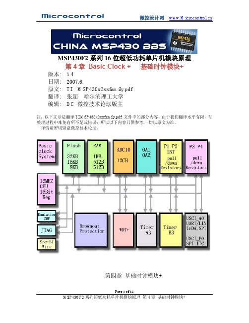
Page 1 of 12MSP430F2系列16位超低功耗单片机模块原理第4章 Basic Clock + 基础时钟模块+版本: 1.4日期: 2007.6.原文: TI MSP430x2xxfamily.pdf翻译: 张超 哈尔滨理工大学编辑: DC 微控技术论坛版主注:以下文章是翻译TI MSP430x2xxfamily.pdf 文件中的部分内容。
由于我们翻译水平有限,有整理过程中难免有所不足或错误;所以以下内容只供参考.一切以原文为准。
详情请密切留意微控技术论坛。
第四章 基础时钟模块+4.1基础时钟模块+介绍基础时钟模块+支持低系统消耗和超低功耗。
采用三种片内时钟信号,用户可以选择合适的性能和低功耗。
基础时钟模块只需接一个外部电阻、一个或两个外部晶体、或者用振荡器,通过软件控制。
基础时钟模块+有4个时钟源:LFXT1CLK:由低频时钟晶体或外接32768Hz时钟源产生的低频/高频振荡器或由标准晶体、振荡器,或外部400KH z~16M Hz的外部时钟源提供。
XT2CLK:可供选择的高频振荡器,由标准晶体、振荡器,或外部400KH z~16M Hz的外部时钟源提供。
DCOCLK:片内可数字控制的振荡器。
VLOCLK:片内超低功耗、12KH z的低频振荡器。
基础时钟模块可提供的三种时钟信号:ACLK:辅助时钟。
ACLK由软件选择来自LFXT1CLK和VLOCLK之一的时钟信号。
ACLK 经1,2,4,8分频后得到。
ACLK可由软件选作各个外围模块。
MCLK:主时钟。
MCLK由软件选择来自LFXT1CLK,VLOCLK,XT2CLK(如果片内提供),DCOCLK之一的时钟信号。
MCLK由1,2,4,8分频得到。
MCLK用于CPU和系统。
SMCLK:子系统时钟。
SMCLK由软件选择来自LFXT1CLK,VLOCLK,XT2CLK(片内提供),DCOCLK之一的时钟信号。
SMCLK由1,2,4,8分频得到。
MSP430F4XX中文技术手册

– MSP430F412: 4KB + 256B Flash Memory,256B RAM;
– MSP430F413: 8KB + 256B Flash Memory,256B RAM;
MSP430F2XX中文手册(加了标签) 1..MSP430体系结构

MSP430F2系列16位超低功耗单片机模块原理第1章MSP430体系结构版本: 1.3日期: 2007.4.原文: TI MSP430x2xxfamily.pdf翻译: 袁德纯编辑: DC 微控论坛版主注:以下文章是翻译TI MSP430x2xxfamily.pdf 文件中的部分内容。
由于我们翻译水平有限,有整理过程中难免有所不足或错误;所以以下内容只供参考.一切以原文为准。
详情请密切留意微控技术论坛。
Page 1 of 7第一章 MSP430的体系结构本章主要描述了MSP430的体系结构本章内容目录1.1MSP430的体系结构1.2可编程时钟系统1.3嵌入式仿真环境1.4地址空间1.5MSP430X2XX系列的提高1.1MSP430的体系结构将MSP430内部的16位精简指令集的CPU通过冯.诺依曼结构的地址总线和数据总线连接到外围设备和可编程时钟系统。
由于有一个先进的CPU配合具有标准组件存储印象的模拟和数字的外围设备,使得MSP430可用于处理混合信号。
MSP430x2xx系列的主要特性如下:◆超低功耗延长了电池的使用寿命●保持RAM 0.1uA●实时时钟模式 0.8uA●MIPS运行 250uA◆理想精确的模拟信号测量●门控比较定时器测量电阻类元件◆16位的精简指令集的CPU全新应用●更大的寄存器空间消除了运行空间的瓶颈●紧凑的核结构设计减少了功耗、降低了成本●使得高水平的编程更优化●27条核心指令和7种寻址方式●强大的矢量中断能力◆系统内的可编程FLASH使改变代码、在线升级和数据载入更灵活1.2 可编程时钟系统时钟系统是为电池供电系统而特别设计的。
只需要一个32KHZ的晶振就可以直接驱动一个低频的辅助时钟(ACLK)。
ACLK可工作于实时时钟模式,并具能够自我唤醒。
内部集成了一个DCO使主时钟(MCLK)可以被CPU和其他的高速外围设备所使用。
由于有了DCO,使得一个窄脉冲在少于2US 的时间内就可以将MSP430唤醒CPU工作。