单片机设计外文翻译
单片机毕业设计外文翻译--数据传送指令
外文资料Data Transfer TechniquesThe actual transfer of data between the microcomputer and external and external devices is commonly carried out using three different techniques:(1)ling;(2)errupters; (3)emory access;These techniques can be used individually or in combination..PollingPolling routines are used for programmed input/output purposes.A number of peripheral devices attached to the microcomouter are continuously polled at specified time intervals to determine the device wishes to input data to the microproccssor. Similarly, for the transfer of data to an output device,the state of its buffer is checked to determine if it is empty and ready to receive the data. A soft program is required to check the state of the peripheral devices. Hardware flaga are used to indacate the send or receive condition of the peripheral. If a device is ready to transfer the data, then an appropriate software routine is used to service that particular device so that data transfer can take place .It is necessary to ensure that none of the data from any of the peripherals are lost while the polling routines or any the peripheral devices servicing routines are being executed. The probability of loseing data is very small since most perpheral are slow deices. Other techniques, such as direct memory access(DMA) , can be used to achieve high-speed data transfer from a given peripheral.Polled input/output is very simple and common method of data transfer which does not require any additional logic circuitry.The only requirement is for an efficient program which is executed at very high speed.Interrupted Intput/outputThe polling procedure is a form of time-sharing whereby the facilities of the computer are shared between a numbers of uses. The computer continually polls each of the terminals, and serves a terminal for a specified period of time before moving on to the next one. This procedure is inefficient because system overheads are incurred in polling all the perpheral devices irrespective of the actual need. The time available for the processing of the real-time requirements of process control system in which a particular device might require urgent attention while the processor is servicing another input/output device. In some circumstances the actual data might be lost. These difficulties can be overcome by using the hardware interrupt input/output system. The output of the microcomputer system can be increased substantially by using such interrupts, since an input/output device is serviced only after it indicates that it is ready to send or receive data.This request for input/output can occur at any time, i.e. in an asynchronous mode,and the devices indicates this by seting up an interrupt flag. The microprocessor acknowledges the interrupt, completes the execution of the currentinstruction, saves the content of the registers and then servieces the requesting devices by transferring control to an appropriate intput/output routine. Once the peripheral device has been serviced, the control is transferred back to the original program which resumes execution from the point at which it was interrupted.Some real-time control applications involve the use of critical programs which must not be interrupted during their execution. Some of the interrupted are trivial which others have to be serviced. For example, data input can be delayed which alarms muse be raised immediately.Differernt types of interrupts, maskable and non-maskable,can be used to overcome these difficulties. Software programs are used to enable or disable a maskable interrupt. Thus,if the maskable interrupt. Thus, if the maskable interrupt has been disabled,the microprocessor will ignore the interrupt request. A non-maskable interrupt has to be acknowdged and serviced by the microprocessor.The interrupt used in a microprocessor system might be a fixed interrupt or a vectored interrupt.A fixed interrupt requires relatively simple hardware. The flag is set on the interrupt line to indicate that service is required. If there is only one device attached to interrupt line ,then the control will be transferred to a fixed memory location which provide the program for servicing that device. When a number of of devices are attached to a given interrupt line, each with its own servicing routine, then the peripheral responsible for the interrupt has to be identifed. Thus a polling routine examination must be used to detect the peripheral requiring service and then determine the memory location at which the program for servicing that device starts. Multiple interrupt lines can be used tovercome these difficulties.Interrupts with multiple lines provide the addresses of different memory locations to which the program should transfer in response to an interrupt on a particular It would be necessary to use as many lines as the number of interrupts or resort to polling routines if more than one device is attached to the same interrupts line .A preferred alternative is to use a vectored interrupt whereby the interrupting device is directly identifed .This device identification can be used to to look up the starting memory location of the service routine for that device. Some vectored interrupts not only identify the interrupting device,butalse provide the starting memory location of the service routine to which the program should jump.Thus the address of the memory location, stored in the peripheral controller ,is placed on the data bus and used for transfering the controller.A system with only one device which can interrupt the normal work of the microcomputer is a very simple one and the particular interrupt can be readily serviced. In practice a large number of devices can provide interrupt requests to the microcomputer .Under normal circumstances, it is likely that two or more devices may provide an interrupt request at the same time.It then becomes necessaryto decide the priority to be allocated to individual interrupt request .A number of procedures can be used for priority allocation purposes.Priorities can be allocated to peripherals attached to a single interrupt line by using a simple daisy chain procedure. Once interrupt, the microcomputer sends a signal to the first device in the daisy If it is the interrupting device ,then it will provide the memory address of its service routine and the signal will not be passed on to the other way round devices in the daisy chain. If, however ,the first device did not cause the interrupt,then the massage will be passed on to the next device. This procedures is repeated until the interrupting device is located. Clearly the first floor device in the daisy chain will have highest priority ,followed by the next one and so on. Once an interrupt request has been acknowledge and is being serviced all the other interrupt either have to be disable or higher priority interrupts must be allowed to break into the current service routine .An alternative to daisy chains is to use priority interrupt circuits which identify and service the device with highest priority. Level 0 means highest priority,followed by level 1, level 2 and so on. These priority interrupt circuits identify up to 8 interrupt level by means of a 3-bit code which can be inspected by the microprocessor.Since event such as power failure must be identified quickly and alarms must be raised as soon as possible, these sub-systems are attached to higher priority interrupts. Similarly, other peripherals requiring fast response can be alloacted higher priority than slow-speed peripherals. Facilities exist for the programmer to mask selectively one or more interrupt levels. When an interrupt is being serviced and another interrupt tasks place, then the priority of the new interrupt is compared with the priority of the existing interrupt. A higher priority interrupt is allowed to suspend the servicing of the current interrupt, otherwise the lower priority interrupt will until the higher priority one has serviced.Some of the currently available priority interrupt circuits carry out far more than the identification of the highest priority device which requires attention. Then will also provide the address of the memory location to which the control should be transferred. If two interrupts occur simultaneously, the device serviced by the microcessor program has the higher priority.Direct Memory AccessWhile interrupted input/output throughput rate is higher than the throughput applications requiring fast data transfering. Direct memory access (DMA) techniques bypass the central processing unit and substantially increase the data transfer rate which can be as high as the memory cycle time allows. The other limiting factor is the speed of the peripheral device. This technique can be used to write data required at high speeds or for transfers between the memory and the mass storage devices attached to the microcomputer. DMA involves the isolation of all devices, other than the single device to be used to for data transfers, from the memory which the data trantsfer between the memory andthe appropriate peripheral is taking place. Special purpose DMA controllers are used to achieve this high-speed block data trantfer. The direct memory access controller requires the use of the address and data buses to carry out the transfer.Direct memory access operation can take place in different modes. It is possible to suspend the normal operations of the microcomputer completely for the period of time during which direct memory access, operations are being carried out. In this particular type of direct memory access, the peripheral wishing to carry out high-speed data transfer informs the DMA controller by means of an interrupt signal. The controler has to obtain control of the data and address buses before the high-speed data trantsfer can take place. This is achieved by sending a HOLD signal to the microcomputer which suspends its operation after executing the current instruction..Control of the data and address of the memory location at which the block starts and the number of words to be transferred .Data is then transferred between the memory and the external device. During this data transfer period, the microcomputer does not carry out any other operation. This type of DMA operation, referred to as the visible or burst mode, is very fast and frequently used in microcomputer systems. However, the speed of operation of the microcessor is reduced.Another mode of direct memory access used in large systems involves the stealing of cycles during which the microprocessor is carrying out other tasks which do not require access to the memory and the data bus is not being used. Data is trantsferred one byte at a time. The cycle steaking can be trantsparent to the microcomputer in the sense that the normal operation of the processor are not suspended. This mode of DMA operation requires that CPU and the external device must not attempt to gin access to the memory at the same time.The vast majority of the availzble microprocessor have DMA facilities and suitable LST-based DMA controller chips are obteainable. Sophisticated systems make use of dedicated microcessor chips as DMA controlers.To summarize,the three input/output techniques discussed here have their own advantages and disadvantages, and are suitable for connecting to different types of devices.The programmed input/output is suitable for use with fast devices which are regularly providing data to the microcomputer.Interrupted input/output can be used with slow peripherals such as teletypewriters.High-speed data transfer between the memory and external storage devices,such as floppy disca,can be achieved by using direct memory access.From Microprocessors and Their Manufacturing Application by A.K.K.ochhar and N.D.Burns数据传送指令通常,微机与外设间的数据的传送用三种不同的方法进行:(1)查询;(2)中断;(3)直接存储器存储。
单片机设计外文文献翻译(含中英文)
附录A 外文翻译——AT89S52/AT89S51技术手册AT89S52译文主要性能与MCS-51单片机产品兼容8K字节在系统可编程Flash存储器1000次擦写周期全静态操作:0Hz~33Hz三级加密程序存储器32个可编程I/O口线三个16位定时器/计数器八个中断源全双工UART串行通道低功耗空闲和掉电模式掉电后中断可唤醒看门狗定时器双数据指针掉电标识符功能特性描述AT89S52是一种低功耗、高性能CMOS8位微控制器,具有8K在系统可编程Flash 存储器。
使用Atmel公司高密度非易失性存储器技术制造,与工业80C51产品指令和引脚完全兼容。
片上Flash 允许程序存储器在系统可编程,亦适于常规编程器。
在单芯片上,拥有灵巧的8位CPU和在系统可编程Flash,使得AT89S52为众多嵌入式控制应用系统提供高灵活、超有效的解决方案。
AT89S52具有以下标准功能:8k字节Flash,256字节RAM,32位I/O口线,看门狗定时器,2个数据指针,三个16位定时器/计数器,一个6向量2级中断结构,全双工串行口,片内晶振及时钟电路。
另外,AT89S52可降至0Hz静态逻辑操作,支持2种软件可选择节电模式。
空闲模式下,CPU停止工作,允许RAM、定时器/计数器、串口、中断继续工作。
掉电保护方式下,RAM内容被保存,振荡器被冻结,单片机一切工作停止,直到下一个中断或硬件复位为止。
引脚结构方框图VCC : 电源GND :地P0口:P0口是一个8位漏极开路的双向I/O口。
作为输出口,每位能驱动8个TTL逻辑电平。
对P0端口写“1”时,引脚用作高阻抗输入。
当访问外部程序和数据存储器时,P0口也被作为低8位地址/数据复用。
在这种模式下,P0具有内部上拉电阻。
在flash编程时,P0口也用来接收指令字节;在程序校验时,输出指令字节。
程序校验时,需要外部上拉电阻。
P1口:P1 口是一个具有内部上拉电阻的8位双向I/O 口,p1 输出缓冲器能驱动4个TTL 逻辑电平。
单片机基础毕业设计外文翻译
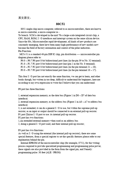
本科生毕业设计(论文)外文翻译毕业设计题目:外文题目:Fundamentals of Single-chip Microcomputer 译文题目:单片机基础学院:信息科学与工程学院专业班级:电子信息工程0802班学生姓名:指导教师:外文原文Fundamentals of Single-chip MicrocomputerDr. Dobbs MacintoshJournalAbstractT h e s i n gl e-chi p m i c r o com pu t er i s t h e cul m i na t i on of bo t h t h e d e v el opm e nt o f t h e di gi t al c om p ut e r a nd t h e i nt e gra t e d c i r c ui t a rgu a b l y t h e t ow m o st s i gn i fi c ant i nv en t i on s of t h e 20t h ce n t u r y .T h es e t o w t yp e s o f a rc hi t e c t u r e a r e fo un d i n s i n gl e-c hi p m i c r o com pu t e r.S om e e m p l o y t h e s pl i t p ro gr a m/d at a m em o r y o f t h e H a r v a rd a r ch i t e ct u r e, s ho wn i n F i g.3-5A-1, ot h er s f o l l o w t he p hi l o so ph y,w i d e l y a d a p t ed f o r ge n e r al-pu rp os e com p ut e rs and m i c r op r oc e s s o rs,of m ak i n g n o l o gi c al di s t i nc t i on be t w ee n p ro gr a m a n d d at a m em o r y a s i n t h e P r i n c et on ar c hi t e ct u r e.In ge n e r a l t er m s a si n gl e-c hi p m i cro c om put e r i s c ha r ac t e ri z ed b y t h e i n co r po r at i o n o f al l t h e u ni t s o f a c om put e r i n t o a s i n gl e d e vi c e.Keyword: Single-chip Microcomputer ROM RAM Programming Algorithm Features• Compatible with MCS-51™ Products• 4K Bytes of In-System Reprogrammable Flash Memory– Endurance: 1,000 Write/Erase Cycles• Fully Static Operation: 0 Hz to 24 MHz• Three-level Program Memory Lock• 128 x 8-bit Internal RAM• 32 Programmable I/O Lines• Two 16-bit Timer/Counters• Six Interrupt Sources• Programmable Serial Channel• Low-power Idle and Power-down ModesDescriptionThe AT89C51 is a low-power, high-performance CMOS 8-bit microcomputer with 4Kbytes of Flash programmable and erasable read only memory (PEROM). The deviceis manufactured using Atmel’s high-density nonvolatile memory technology and iscompatible with the industry-standard MCS-51 instruction set and pinout. Theon-chipFlash allows the program memory to be reprogrammed in-system or by a conventionalnonvolatile memory programmer. By combining a versatile 8-bit CPU with Flashon a monolithic chip, the Atmel AT89C51 is a powerful microcomputer which providesa highly-flexible and cost-effective solution to many embedded control applications.The AT89C51 provides the following standard features: 4Kbytes of Flash, 128 bytes of RAM, 32 I/O lines, two 16-bittimer/counters, a five vector two-level interrupt architecture,a full duplex serial port, on-chip oscillator and clock circuitry.In addition, the AT89C51 is designed with static logicfor operation down to zero frequency and supports twosoftware selectable power saving modes. The Idle Modestops the CPU while allowing the RAM, timer/counters,serial port and interrupt system to continue functioning. ThePower-down Mode saves the RAM contents but freezesthe oscillator disabling all other chip functions until the nexthardware reset.Pin ConfigurationsBlock DiagramPin DescriptionVCCSupply voltage.GNDGround.Port 0Port 0 is an 8-bit open-drain bi-directional I/O port. As anoutput port, each pin can sink eight TTL inputs. When 1sare written to port 0 pins, the pins can be used as highimpedanceinputs.Port 0 may also be configured to be the multiplexed loworderaddress/data bus during accesses to external programand data memory. In this mode P0 has internalpullups.Port 0 also receives the code bytes during Flash programming,and outputs the code bytes during programverification. External pullups are required during program verification.Port 1Port 1 is an 8-bit bi-directional I/O port with internal pullups.The Port 1 output buffers can sink/source four TTL inputs.When 1s are written to Port 1 pins they are pulled high bythe internal pullups and can be used as inputs. As inputs,Port 1 pins that are externally being pulled low will source current (IIL) because of the internal pullups.Port 1 also receives the low-order address bytes during Flash programming and verification.Port 2Port 2 is an 8-bit bi-directional I/O port with internal pullups.The Port 2 output buffers can sink/source four TTL inputs.When 1s are written to Port 2 pins they are pulled high by the internal pullups and can be used as inputs. As inputs, Port 2 pins that are externally being pulled low will source current (IIL) because of the internal pullups.Port 2 emits the high-order address byte during fetches from external program memory and during accesses to external data memory that use 16-bit addresses (MOVX @DPTR). In this application, it uses strong internal pullups when emitting 1s. During accesses to external data memory that use 8-bit addresses (MOVX @ RI), Port 2 emits the contents of the P2 Special Function Register.Port 2 also receives the high-orderaddress bits and some control signals during Flash programming and verification.Port 3Port 3 is an 8-bit bi-directional I/O port with internal pullups.The Port 3 output buffers can sink/source four TTL inputs.When 1s are written to Port 3 pins they are pulled high by the internal pullups and can be used as inputs. As inputs,Port 3 pins that are externally being pulled low will source current (IIL) because of the pullups.Port 3 also serves the functions of various special features of the AT89C51 as listed below:Port 3 also receives some control signals for Flash programmingand verification.ALE/PROGAddress Latch Enable output pulse for latching the low byte of the address during accesses to external memory. This pin is also the program pulse input (PROG) during Flash programming.In normal operation ALE is emitted at a constant rate of 1/6the oscillator frequency, and may be used for external timing or clocking purposes. Note, however, that one ALE pulse is skipped during each access to external Data Memory.If desired, ALE operation can be disabled by setting bit 0 of SFR location 8EH. With the bit set, ALE is active only during a MOVX or MOVC instruction. Otherwise, the pin is weakly pulled high. Setting the ALE-disable bit has no effect if the microcontroller is in external execution mode.PSENProgram Store Enable is the read strobe to external program memory.When theAT89C51 is executing code from external programmemory, PSEN is activated twice each machine cycle, except that two PSEN activations are skipped during each access to external data memory.EA/VPPExternal Access Enable. EA must be strapped to GND in order to enable the device to fetch code from external program memory locations starting at 0000H up to FFFFH.Note, however, that if lock bit 1 is programmed, EA will be internally latched on reset. EA should be strapped to VCC for internal program executions. This pin also receives the 12-volt programming enable voltage (VPP) during Flash programming, for parts that require 12-volt VPP.XTAL1Input to the inverting oscillator amplifier and input to the internal clock operating circuit.XTAL2Output from the inverting oscillator amplifier.Oscillator CharacteristicsXTAL1 and XTAL2 are the input and output, respectively,of an inverting amplifier which can be configured for use as an on-chip oscillator, as shown in Figure 1. Either a quartz crystal or ceramic resonator may be used. To drive the device from an external clock source, XTAL2 should be left unconnected while XTAL1 is driven as shown in Figure 2. There are no requirements on the duty cycle of the external clock signal, since the input to the internal clocking circuitry is through a divide-by-two flip-flop, but minimum and maximum voltage high and low time specifications must be observed.Idle ModeIn idle mode, the CPU puts itself to sleep while all the onchip peripherals remain active. The mode is invoked by software. The content of the on-chip RAM and all the special functions registers remain unchanged during this mode. The idle mode can be terminated by any enabled interrupt or by a hardware reset. It should be noted that when idle is terminated by a hard ware reset, the device normally resumes programexecution,from where it left off, up to two machine cycles before the internal reset algorithm takes control. On-chip hardware inhibits access to internal RAM in this event, but access to the port pins is not inhibited. To eliminate the possibility of an unexpected write to a port pin when Idle is terminated by reset, the instruction following the one that invokes Idle should not be one that writes to a port pin or to external memory.Figure 1. Oscillator ConnectionsFigure 2. External Clock Drive ConfigurationPower-down ModeIn the power-down mode, the oscillator is stopped, and the instruction that invokes power-down is the last instruction executed. The on-chip RAM and Special Function Registers retain their values until the power-down mode is terminated. The only exit from power-down is a hardware reset. Reset redefines the SFRs but does not change the on-chip RAM. The reset should not be activated before VCC is restored to its normal operating level and must be held active long enough to allow the oscillator to restart and stabilize.Program Memory Lock BitsOn the chip are three lock bits which can be left unprogrammed (U) or can be programmed (P) to obtain the additional features listed in the table below.When lock bit 1 is programmed, the logic level at the EA pin is sampled and latched during reset. If the device is powered up without a reset, the latch initializes to a random value, and holds that value until reset is activated. It is necessary that the latched value of EA be in agreement with the current logic level at that pin in order for the device to function properly.Programming the FlashThe AT89C51 is normally shipped with the on-chip Flash memory array in the erased state (that is, contents = FFH) and ready to be programmed. The programming interface accepts either a high-voltage (12-volt) or a low-voltage (VCC) program enable signal. The low-voltage programming mode provides a convenient way to program theAT89C51 inside the user’s system, while the high-voltage programming mode is compatible with conventional thirdparty Flash or EPROM programmers. The AT89C51 is shipped with either the high-voltage or low-voltage programming mode enabled. The respective top-side marking and device signature codes are listed in the following table.The AT89C51 code memory array is programmed byte-bybyte in either programming mode. To program any nonblank byte in the on-chip Flash Memory, the entire memory must be erased using the Chip Erase Mode.Programming Algorithm: Before programming the AT89C51, the address, data and control signals should be set up according to the Flash programming mode table and Figure 3 and Figure 4. To program the AT89C51, take the following steps.1. Input the desired memory location on the address lines.2. Input the appropriate data byte on the data lines.3. Activate the correct combination of control signals.4. Raise EA/VPP to 12V for the high-voltage programming mode.5. Pulse ALE/PROG once to program a byte in the Flash array or the lock bits. The byte-write cycle is self-timed and typically takes no more than 1.5 ms.Repeat steps 1 through 5, changing the address and data for the entire array or until the end of the object file is reached.Data Polling: The AT89C51 features Data Polling to indicate the end of a write cycle. During a write cycle, an attempted read of the last byte written will result in the complement of the written datum on PO.7. Once the write cycle has been completed, true data are valid on all outputs, and the next cycle may begin. Data Polling may begin any time after a write cycle has been initiated.Ready/Busy: The progress of byte programming can also be monitored by theRDY/BSY output signal. P3.4 is pulled low after ALE goes high during programming to indicate BUSY. P3.4 is pulled high again when programming is done to indicate READY.Program Verify: If lock bits LB1 and LB2 have not been programmed, the programmed code data can be read back via the address and data lines for verification. The lock bits cannot be verified directly. Verification of the lock bits is achieved by observing that their features are enabled.Chip Erase: The entire Flash array is erased electrically by using the proper combination of control signals and by holding ALE/PROG low for 10 ms. The code array is written with all “1”s. The chip erase operation must be executed before the code memory can be re-programmed.Reading the Signature Bytes: The signature bytes are read by the same procedure as a normal verification of locations 030H, 031H, and 032H, except that P3.6 and P3.7 must be pulled to a logic low. The values returned are as follows.(030H) = 1EH indicates manufactured by Atmel(031H) = 51H indicates 89C51(032H) = FFH indicates 12V programming(032H) = 05H indicates 5V programmingProgramming InterfaceEvery code byte in the Flash array can be written and the entire array can be erasedby using the appropriate combination of control signals. The write operation cycle is selftimed and once initiated, will automatically time itself to completion. All major programming vendors offer worldwide support for the Atmel microcontroller series. Please contact your local programming vendor for the appropriate software revision.外文资料翻译译文单片机基础摘要:单片机是电脑和集成电路发展的巅峰,有据可查的是它们也是20世纪最意义的两大发明。
单片机设计外文翻译--从无线电世界到单片机世界

From the world of radio in the world to a single chipModern computer technology, industrial revolution, the world economy from the capital into the economy to knowledge economy. Field in the electronic world, from the 20th century into the era of radio to computer technology in the 21st century as the center of the intelligent modern era of electronic systems. The basic core of modern electronic systems are embedded computer systems (referred to as embedded systems), while the microcontroller is the most typical and most extensive and most popular embedded systems.First, radio has created generations of excellence in the world Fifties and sixties in the 20th century, the most representative of the advanced electronic technology is wireless technology, including radio broadcasting, radio, wireless communications (telegraph), Amateur Radio, radio positioning, navigation and other telemetry, remote control, remote technology. Early that these electronic technology led many young people into the wonderful digital world, radio show was a wonderful life, the prospects for science and technology. Electronics began to form a new discipline. Radio electronics, wireless communications began e-world journey.Radio technology not only as a representative of advanced science and technology at that time, but also from popular to professional fields of science, attracting the young people and enable them to find a lot of fun. Ore from the bedside to the superheterodyne radio radio; report issued from the radio amateur radio stations; from the telephone, electric bell to the radio control model. Became popular youth radio technology, science and technology education is the most popular and most extensive content. So far, many of the older generation of engineers, experts, Professor of the year are radio enthusiasts. Fun radio technology, radio technology, comprehensive training, from basic principles of electronics, electronic components to the radio-based remote control, telemetry, remote electronic systems, has trained several generations of technological excellence.Second, from the popularity of the radio era to era of electronic technologyThe early radio technology to promote the development of electronic technology, most notably electronic vacuum tube technology to semiconductor electronictechnology. Semiconductor technology to realize the active device miniaturization and low cost, so more popular with radio technology and innovation, and to greatly broaden the number of non-radio-control areas.The development of semiconductor technology lead to the production of integrated circuit, forming the modern electronic technology leap from discrete electronics into the era of era of integrated circuits. Electronic design engineers no longer use the discrete electronic components designed circuit modules, and direct selection of integrated circuit components constitute a single system. They freed the design of the circuit unit dedicated to system design, greatly liberating the productive forces of science and technology, promote the wider spread of electronic systems.Semiconductor integrated circuits in the basic digital logic circuits first breakthrough.A large number of digital logic circuits, such as gates, counters, timers, shift registers, and analog switches, comparators, etc., for the electronic digital control provides excellent conditions for the traditional mechanical control to electronic control. Power electronic devices and sensor technology to make the original to the radio as the center of electronic technology turned to mechanical engineering in the field of digital control systems, testing in the field of information collection, movement of electrical mechanical servo drive control object.Semiconductor and integrated circuit technology will bring us a universal age of electronic technology, wireless technology as the field of electronic technology a part of.70 years into the 20th century, large scale integrated circuit appeared to promote the conventional electronic circuit unit-specific electronic systems development. Many electronic systems unit into a dedicated integrated devices such as radios, electronic clocks, calculators, electronic engineers in these areas from the circuit, the system designed to debug into the device selection, peripheral device adapter work. Electronic technology, and electronic products enriched, electronic engineers to reduce the difficulty, but at the same time, radio technology, electronic technology has weakened the charm. The development of semiconductor integrated circuits classical electronic systems are maturing, remain in the large scale integrated circuit other thanthe shrinking of electronic technology, electronic technology is not the old days of radio fun times and comprehensive engineering training.Third, from the classic era of electronic technology to modern electronic technology of the times80 years into the 20th century, the century of economic change is the most important revolution in the computer. The computer revolution in the most important sign is the birth of the computer embedded applications. Modern computer numerical requirements should be born. A long period of time, is to develop the massive computer numerical duty. But the computer shows the logic operation, processing, control, attracting experts in the field of electronic control, they want development to meet the control object requirements of embedded applications, computer systems. If you meet the massive data-processing computer system known as general-purpose computer system, then the system can be the embedded object (such as ships, aircraft, motorcycles, etc.) in a computer system called the embedded computer. Clearly, both the direction of technology development are different. The former requires massive data storage, handling, processing and analysis of high-speed data transmission; while the latter requires reliable operation in the target environment, the external physical parameters on high-speed acquisition, analysis and processing logic and the rapid control of external objects. It will add an early general-purpose computer data acquisition unit, the output driver circuit reluctance to form a heat treatment furnace temperature control system. This general-purpose computer system is not possible for most of the electronic system used, and to make general-purpose computer system meets the requirements of embedded applications, will inevitably affect the development of high-speed numeric processing. In order to solve the contradiction between the development of computer technology, in the 20th century 70s, semiconductor experts another way, in full accordance with the electronic system embedded computer application requirements, a micro-computer's basic system on a chip, the formation of the early SCM (Single Chip Microcomputer). After the advent of single chip in the computer industry began to appear in the general-purpose computer systems and embedded systems the two branches. Since then, both the embedded system, or general-purpose computer systems have been developed rapidly.Although the early general-purpose computer converted the embedded computer systems, and real embedded system began in the emergence of SCM. Because the microcontroller is designed specifically for embedded applications, the MCU can only achieve embedded applications. MCU embedded applications that best meet environmental requirements, for example, chip-level physical space, large-scale integrated circuits low-cost, good peripheral interface bus and outstanding control of instruction.A computer system microcontroller core, embedded electronic systems, intelligent electronic systems for the foundation. Therefore, the current single chip electronic system in widespread use of electronic systems to enable rapid transition to the classical modern intelligent electronic systems.4, single chip to create the modern era of electronic systemsA microcontroller and embedded systemsEmbedded computer systems from embedded applications, embedded systems for early general-purpose computer adapted to the object system embedded in a variety of electronic systems, such as the ship's autopilot, engine monitoring systems. Embedded system is primarily a computer system, followed by it being embedded into the object system, objects in the object system to achieve required data collection, processing, status display, the output control functions, as embedded in the object system, embedded system computer does not have an independent form and function of the computer. SCM is entirely in accordance with the requirements of embedded system design, so SCM is the most typical embedded systems. SCM is the early application of technical requirements in accordance with the design of embedded computer chip integration, hence the name single chip. Subsequently, the MCU embedded applications to meet the growing demands of its control functions and peripheral interface functions, in particular, highlight the control function, so has international name the single chip microcontroller (MCU, Microcontroller Unit).2 MCU modern electronic systems consisting of electronic systems will become mainstreamMCU is a device-level computer systems, it can be embedded into any object system to achieve intelligent control. Small to micro-machinery, such as watches,hearing aids. Low-cost integrated device-level, low-to a few dollars, ten dollars, enough to spread to many civilian SCM appliances, electronic toys to go. SCM constitutes a modern electronic systems has in-depth to the households, are changing our lives, such as home audio, televisions, washing machines, microwave ovens, telephones, security systems, and air conditioners. SCM innovation the original electronic systems, such as microwave ovens use SCM, it can easily set the clock, the program memory, power control; air conditioner after use of SCM is not only convenient for remote parameter setting, running automatically transform, frequency control can be achieved. At present, many household appliances such as VCD, DVD only single chip to achieve its function may occur before.3 Embedded Systems led the entire electronics industryCurrent electronic components industry, in addition to microprocessors, embedded system devices, the most modern electronic systems around the supporting components industries, such as keys used to meet the human-computer interaction, LED / LCD display drivers, LED / LCD display units, voice integrated device, etc., to meet the requirements of data acquisition channel digital sensor, ADC, data acquisition module, signal conditioning modules to meet the servo drive control in the DAC, solid state relays, stepper motor controller, frequency control unit, etc., to meet the communication requirements various bus driver, level converters.Electronic components in the embedded systems world, driven by embedded applications along fully meet requirements of modern electronic systems development. This makes the original classic world of increasingly small electronic systems. Practitioners in the various electronic systems to modern electronic systems as early as possible to stay.5, SCM will create a new generation of electronic eliteIf the 50's, radio has created several generations of the world elite, then today's SCM will create a new generation of e-world elite.A single chip with you to the intelligent electronicsIf we as a dead classic electronic system electronic system, then the intelligent modern electronic systems is a "life" of the electronic system. Application System of hardware, electronic systems, "body", microcontroller applications, the applicationgives it "life." For example, in the design of intelligent machines monitor display, it can boot the system self-test results show, not to enter the work shows a variety of stand-by state, equipment run-time display running processes, work can be displayed after the end of the current results, self results, raw data, reports and other various processing. Unattended, it can run automatically given a variety of functions.Intelligent electronic systems for the endless realm, often without additional hardware resources can achieve all kinds of renovated function. It is also present in many household appliances feature a large number of additional factors.2 single chip computer with you to the industrial areaThe 21st century is the century of humanity into the computer age, many people are not used in the manufacture of computer is the computer. People using the computer, only the people engaged in embedded system applications really into the internal computer system hardware and software systems, can we truly understand the nature of the computer's intelligence and grasp the knowledge of intelligent design. MCU applications starting from the learning technology applications in today's computer software training, hardware and technical personnel of one of the best roads.3 SCM bring you into the most attractive in the digital worldCharming single chip to enable you to experience the true meaning of the computer, you can design intelligent microcontroller hands-on toys, different applications can be designed to achieve different functions. Both software design and hardware making there, both mental and physical, but also hands. Primary level can develop intelligent toys, with macro programming. Intermediate levels can develop some intelligent controller, such as computer mouse, smart cars, all kinds of remote control model. High levels can be developed robots, such as robot soccer, the development of industrial control units, network communications, and high-level language with assembly language or design application. Microcontroller and embedded systems around the formation of the future of the electronics industry, will provide a vast world of electronic fans, an even broader than the current wireless world, richer, more durable, more attractive in the digital world. Plunge into the microcontroller in the world to, will benefit your life.MCU AttacksCurrently, there are four single chip attack technique, namely:(1) software attackThe technology is commonly used processor communication interface and use protocol, encryption algorithm or the algorithm of security vulnerabilities to attack. The success of software attack is a typical example of the early ATMEL AT89C MCU attacks. Attacker single chip erase operation of the timing design flaw, erase the encryption used by ourselves locked in place, the next stop on-chip program memory data erase operation, thus bringing into too close a single chip SCM not encrypted, and then use the programmer to read out chip program.(2) electronic detection of attacksThe technology is usually a high time resolution to monitor the processor during normal operation of all power and interface simulation features, and by monitoring the electromagnetic radiation characteristics of it to attack. Because SCM is an active electronic device, when it executes a different command, the corresponding changes in the power consumption accordingly. This through the use of special electronic measuring instruments and mathematical statistical analysis and detection of these changes, you can access key information specific microcontroller.(3) fault generation technologyAbnormal working conditions of the technology used to make the processor errors, and provide additional access to attack. Produce the most widely used means of attack, including the fault of the impact and the clock voltage shock. Low voltage and high voltage protection circuit attack can be used to prohibit the work of processor execution errors or enforcement action. Clock transition may reset the transient protection circuit will not damage the protected information. Power and clock transients transition effects in certain single-processor instruction decoding and execution.(4) probeThis technology is directly exposed to chip connection, and then observe, manipulate, interfere with single chip to achieve the attack purpose. For convenience, these four people will attack techniques are divided into two categories is theintrusion type attack (physical attack), such attack requires destruction of package, then use semiconductor test equipment, microscopes and micro-positioning device, in a special laboratory spend hours or even weeks to complete. All of the micro-probe techniques are invasive type attack. The other three methods are non-invasive type attack, attack the MCU will not be physical damage. In some cases, non-invasive-type attacks are particularly dangerous, but because of non-invasive type attacks can usually be made and the necessary equipment to upgrade, so it is cheap.Most non-invasive type attack requires the attacker have a good knowledge of processors and software knowledge. In contrast, the invasive type of probe do not need too much of the initial attack of knowledge, and usually a set of similar technology available to deal with a wide range of productsMCU general process of invasion-type attackInvasive type of attack is thrown off its first chip package. There are two ways to achieve this goal: the first one is completely dissolved out chip package, exposed metal connections. The second is only removed to the top of the plastic package silicon core. The first method is the need to bind to the test fixture on the chip, using bind Taiwan to operate. The second method requires the attacker in addition to a certain degree of knowledge and necessary skills, but also the wisdom and patience, but operate relatively easy.Above the plastic chips can be opened with a knife, epoxy around the chip can be eroded by concentrated nitric acid. Hot concentrated nitric acid will dissolve out without affecting the chip, chip packaging and connection. This process usually very dry conditions, because the presence of water may erode the aluminum wire connections have been exposed.Then, in ultrasonic cleaning of the pool first chip with acetone to remove residual nitric acid, then washed with water to remove salt and dried. No ultrasound pool, are generally skip this step. This case, the chip surface, a bit dirty, but do not affect the operation of UV effects on the chip. The final step is to find the location of the protection fuse and fuse protection under exposure to UV light. General use at least a 100 times magnification microscope, from the programming voltage input pin of the connection tracking in, to find protection fuse. If there is no microscope, theuse of different parts of the chip is exposed to ultraviolet light and observe the results under the simple search mode. Operation applied opaque paper cover to protect the program memory chips are not erased by ultraviolet light. Will protect the fuse exposed under UV light 5 to 10 minutes to destroy the protection bit of the protective effect, use a simple programmer can directly read the contents of program memory.The use of the protective layer to protect the MCU EEPROM cell, using ultraviolet light reset protection circuit is not feasible. For this type of MCU, the general use of micro-probe technology to read the memory contents. In the chip package is opened, the chip placed under the microscope can easily find from the memory circuit connected to other parts of the data bus.For some reason, the chip lock-bit programming mode is not locked in the memory of the visit. Advantage of this flaw on the data lines to probe the above data can be read all you want. In programming mode, restart the process of reading and connect probe to the other data can be read online program and data memory, all of the information.There is also a possible means of attack is the use of microscopy and laser cutting machines and other equipment to find the fuse protection to this part of the circuit tracing and linking all the signal lines. Because of the design defects, so long as cut off from other circuit protection fuse to a one signal line, you can ban the entire protection. For some reason, this thread is very far from the other line, so the use of laser cutting machine can cut the wire without affecting the adjacent line. In this way, using a simple programmer can directly read the contents of program memory.Although the most common single chip microcontroller has fuse blown inside the code protection features, but because of general low-end MCU is not positioning the production of safe products, so they often do not provide targeted preventive measures and the low level of security. MCU applications with a broad, large sales volume, commission processing and transfer of technology between firms frequently spilled a lot of technical data, making use of loopholes in the design of such chips and test interface manufacturer, and by modifying the invasive type fuse protection bits, etc. means of attack or invasion-type attack to read MCU's internal procedureshave become easier.About common single chipSTC microcontrollerSTC's mainly based on the 8051 microcontroller core is a new generation of enhanced MCU, the instruction code is fully compatible with the traditional 8051, 8 to 12 times faster, with ADC, 4 Road, PWM, dual serial ports, a global unique ID, encryption of good, strong anti-interference.PIC Microcontroller:MICROCHIP's products is its prominent feature is a small, low power consumption, reduced instruction set, interference, reliability, strong analog interface, the code of confidentiality is good, most of the chip has its compatible FLASH program memory chips.EMC SCM:Elan's products in Taiwan, with much of the PIC 8-bit microcontroller compatible, and compatible products, resources, compared to the PIC's more, cheap, there are many series of options, but less interference.ATMEL microcontroller (MCU 51):ATMEl company's 8-bit microcontroller with AT89, AT90 two series, AT89 series is the 8-bit Flash microcontroller 8051 is compatible with the static clock mode; AT90 RISC MCU is to enhance the structure, all static methods of work, containing the line can be Flash MCU programming, also known A VR microcontroller.PHLIPIS 51PLC Microcontroller (MCU 51):PHILIPS company's MCU is based on the 80C51 microcontroller core, embedded power-down detection, simulation and on-chip RC oscillator and other functions, which makes 51LPC in highly integrated, low cost, low power design to meet various applications performance requirements.HOLTEK SCM:Sheng Yang, Taiwan Semiconductor's single chip, cheap more categories, but less interference for consumer products.TI company microcontroller (MCU 51):Texas Instruments MSP430 provides the TMS370 and two series of general-purpose microcontroller. TMS370 MCU is the 8-bit CMOS MCU with a variety of storage mode, a variety of external interface mode, suitable for real-time control of complex situations; MSP430 MCU is a low power, high functionality integrated 16-bit low-power microcontroller, especially for applications that require low power consumption occasionsTaiwan Sonix's single, mostly 8-bit machines, some with PIC 8-bit microcontroller compatible, cheap, the system clock frequency may be more options there PMW ADC internal noise filtering within the vibration. Shortcomings RAM space is too small, better anti-interference.从无线电世界到单片机世界现代计算机技术的产业革命,将世界经济从资本经济带入到知识经济时代。
单片机毕业设计外文翻译10
一、外文原文:The single slice machine is also called tiny controller, is because it was used in the industry to control realm at the earliest stage. Single slice machine from inside chip have CPU appropriation processor to develop only since then. At the earliest stage of design the principle is to pass to integrate a great deal of peripherals and CPU in a chip, making calculator system smaller, integrating more easily into complicated of but to mention to request a strict control equipments in the middle. The INTEL Z80 is the processor which designed according to this kind of thought at the earliest stage, from now on, single slice the development of the machine and appropriation processor went by different roads then.The single slice of the earlier period all of machines are 8 or 4.Among them, the INTEL is most successful of 8031, because of in brief dependable but the function was quite good to acquire very big good opinion.Henceforth at 8031 up developed MCS51 serieses a single slice machine system.According to the single slice of this system machine system is still in the extensive usage till now.Because the industry controls the exaltation of[with] realm request, starting appearing 16 single slice machine, but because sex price wanted to don't get a very extensive application than the disregard.Develop greatly along with the consumption electronics product after 90's, the single slice machine technique got a huge exaltation. Along with the extensive application of INTEL i960 serieses especially later ARM series, the 32 single slice machines replaces 16 single slice the high level position of the machine quickly, and gets into an essential market. And traditional of 8 single slice the function of the machine also got to fly to raise soon, handling an ability to compare with to raise few a hundred folds in 80's.Currently, 32 single slice of the high level with main machine already over 300 MHz, the function keeps appropriation processor of making track for the mid 90's, and the common model number factory price drop into to USD 1, tallest carry of model number also only USD 10.The contemporary and single slice machine system has already no longer developed and used just under the naked machine environment, the in great quantities appropriative built-in operate system is applied extensively in the whole seriousness of the single slice is on board. But Be using the high level of handheld PC and cellular phone core processing single slice the machine even can use appropriative Windows and the Linux operate system directly.Single slice the machine ratio appropriation processor is the most suitable to match to apply in the built-in system, so it got the most applications. In fact the single slice machine is an amount the most calculators are in the world. The modern mankind are living medium use of assemble in almost each electronics and machine product have a single slice machine. All have 1-2 single slice machine in the computer accessoriness such as cellular phone, telephone, calculator, home appliances, electronics toy, handheld PC and mouse etc.. And personal computer in would also capable number not a few single slice the machine be working. Provide with morethan 40 departments a single slice machine generally on the car; complicated industry's controlling the top of the system even may has single several hundred pedestals slices machine to work in the meantime! Single slice the amount of the machine not only far above the PC machine and other calculations of comprehensive, even than the mankind's amount still want have another二、翻译内容单片机也被称为微控制器(Microcontroller),是因为它最早被用在工业控制领域。
单片机毕业设计外文文献翻译
英文原文:80C518051 single-chip micro-computer, referred to as microcontrollers, there are known as micro-controller, a micro-computer re -To branch. SCM is developed in the mid 70s a large-scale integrated circuit chip, a CPU, RAM, ROM, I / O interfaces and interrupt system on the same silicon device. Since the 80s, Microcontroller rapid development, all kinds of new products are constantly emerging, there have been many high-performance of new models now become the field of factory automation and control of the pillar industries.Pin Function:MCS-51 is a standard 40-pin DIP IC chip, pin distribution ---- microcontroller pin diagram please refer to:P0.0 ~ P0.7 P0 port 8-bit bidirectional port lines (in the pin 39 to No. 32 terminal). P1.0 ~ P1.7 P1 port 8-bit bidirectional port line (pin 1 in the No. 8 terminal).P2.0 ~ P2.7 P2 port 8-bit bidirectional port lines (in the pin terminal 21 ~ 28).P3.0 ~ P3.7 P3 port 8-bit bidirectional port lines (in the pin terminal 10 ~ 17).This four I / O port has not exactly the same function, we can get to learn, and other books though, but written in too deep, difficult to understand for beginners, here are according to my own expression to write the I believe that you can understand.P0 port has three functions:1, external expansion memory, as the data bus (Figure 1 in D0 ~ D7 of data bus interface)2, external expansion memory, as the address bus (Figure 1 in A0 ~ A7 to address bus interface)3, is not extended, it can do a general I / O to use, but within the supreme pull-up resistor, as an input or output should be connected to an external pull-up resistor.P1 port Zhizuo I / O port to use: its internal pull-up resistor.P2 port has two functions:1,An extended external memory when used as an address bus2, doing a general I / O port used, and their internal pull-up resistor;P3 port has two functions:As well as I / O using the external (the internal pull-up resistor), there are some special features, from a special register to set the specific features please refer to our explanation behind the pin.Internal EPROM of the microcontroller chip (for example, 8751), for the writing process required to provide specialized programming and programming pulse power, these signals are also provided in the form from the signal pin, and Namely: programming pulse: 30 feet (ALE / PROG)Programming voltage (25V): 31 feet (EA / Vpp)In introducing the four I / O port referred to a "pull-up resistor" Then, pull-up resistor is what Dongdong do? What role does he play? Said the resistance that is of course, is a resistor, when as an input, the pull-up resistor pulled its potential, if the input is low you can provide a current source; Therefore, if the P0 port as long as the input, in the high impedance state, only an external pull-up resistor to be effective. ALE / PROG address latch control signal: in a system is extended, ALE is used to control the P0 port output low 8-bit address latch latch get together in order to achieve low address and data segregation. (In the back on the expansion of the curriculum, we will see the 8051 expansion of EEPROM circuit, the ALE and the 74LS373 in Figure G-latches connected to the external CPU to access when the time to lock the address low address, the P0 port output. ALE may be high may also be low, when the ALE is high, allowing address latch signal when accessing external memory, ALE signals a negative transition (from positive to negative) P0 port on the lower eight address signals into the latch. when ALE is low, when, P0 port on the content and the output latch line. on the latch, and we will be introduced later.In the absence of access to external memory during the period, ALE 1 / 6 oscillator frequency output cycle (ie, frequency of 6 points), when access to external memory to 1 / 12 oscillator cycle, the output (12 min frequency). From here we can see that when the system does not extend when the ALE will be 1 / 6 cycle, fixed frequency oscillator output, so can be used as an external clock, or the use of an external timing pulse.PORG pulse input for the program: In the fifth lesson MCU's internal structure and composition, we know that in 8051 within the a 4KB or 8KB of program memory (ROM), ROM's role is to be used to store user needs implementation of the program, then we are into how to write good programs into this ROM in it? Is actually programmed into the pulse input can be written, this pulse input port is PROG. PSEN external program memory read strobe: In reading an external ROM, PSEN low effective, in order to achieve an external ROM module read.1, the internal ROM reading, PSEN is not action;2, external ROM reading at each machine cycle will move twice;3, external RAM read, the two PSEN pulse is skipped will not be output;4, external ROM, and ROM-foot-phase OE.See Figure 2 - (8051 extension 2KB EEPROM circuit in Figure PSEN and expansion ROM in the OE pin-phase)EA / VPP access and sequence memory control signals1, then high time:CPU reads the internal program memory (ROM)Expansion of the external ROM: When reading the internal program memory than0FFFH (8051) 1FFFH (8052) automatically reads the external ROM.2, then low when: CPU to read external program memory (ROM). In the previous study, we are aware, there is no internal ROM MCU 8031, then 8031 microcontroller in the application, this pin is a low level of direct.3,8751 Shaoxie internal EPROM, to make use of this pin input voltage of 21V forShao Xie.RST Reset signal: when the input signal continuously high for more than two machine cycles when it is effective to complete the MCU reset initialization, when the reset program counter PC = 0000H, ie, after reset from the program memory of the 0000H unit to read the first script.External crystal oscillator pins XTAL1 and XTAL2. When using the chip internal clock, this two-pin for external quartz crystal and fine-tuning capacitor; when using an external clock, used to access an external clock pulse signal.VCC: Power Supply +5 V inputVSS: GND Ground.A VR and the pic are 8051 different structures with 8-bit microcontrollers, because structure is different, so assembly instructions are different, but distinct from the useof CISC instruction set of the 8051, they are RISC instruction set, and only a few dozen instructions, most instructions are single instruction cycle instruction, so in the same crystal frequency, faster than the 8051. Another PIC 8-bit microcontroller in previous years, is the world's largest MCU shipments, followed by Freescale microcontroller.ARM is actually 32-bit microcontroller, its internal resources (registers and peripheral functions) than in 8051 and PIC, A VR should be a lot more, with the computer's CPU chip is very close. Commonly used in mobile phones, routers and so on.DSP is actually a special kind of microcontroller, which from 8-32 are available here. It is specifically used to calculate the digital signals. Operation in some formulas, it's fastest computers than the current home of the CPU even faster. For example, the general 32-bit DSP instruction cycle in an op-End a 32-digit x 32-digit product coupled with a 32-digit. Applied to certain pairs of real-time processing requirements of the higher places中文译文:8051单片微型计算机简称为单片机,又称为微型控制器,是微型计算机的一个重要分支。
单片机STM32外文文献翻译、中英文翻译

外文译英文原文:STM32 MicrocontrollerIntroductionRequirements based STM32 family is designed for high-performance, low-cost, low-power embedded applications designed specifically for ARM Cortex-M3 core. According to the performance into two different series: STM32F103 "Enhanced〞 series and STM32F101 "Basic" series. Enhanced Series clock frequency of 72MHz, the highest performance of similar products product; basic clock frequency of 36MHz, 16-bit product prices get more than 16 products significantly enhance the performance and is 16 product users the best choice. Both series have built-in 32K to 128K of flash memory, the difference is the maximum capacity of the SRAM and peripheral combinations. At 72MHz, executing from Flash, STM32 power consumption 36mA, are 32 products on the market s lowest power, the equivalent of 0.5niA/MHz.STM32F103 Performance Characteristics1)Kernel. ARM32 bit CPU, the maximum operating frequency of 72MHz,1.25DMIPS/MHz. Single-cycle multiply and hardware divide.2)Memory. Integrated on-chip 32-512KB of Flash memory. 6-64KB SRAM memory.3)Clock, reset, and power management. 2.0-3.6V power supply and I/O interface, the drive voltage. POR, PDR and programmable voltage detector. 4-16MHz crystal. Embedded factory tuned 8MHz RC oscillator circuit. 40 kHz internal RC oscillator circuit. CPU clock for the PLL. With calibration for the RTC 32kHz crystal.4)Low power consumption. Three kinds of low-power mode. Sleep, stop, standby mode. For RTC and backup registers supply VBAT.5)Debug mode. Serial debugging and JTAG interface.6)Direct data storage. 12-channel direct data storage controller. Supported peripherals: timers, ADC, DAC, SPI, IIC and USART.7)Up to a maximum of 112 fast I / O ports. Depending on the modeL there are 26,37,51,80, and 112 I/O ports, all ports can be mapped to 16 external interrupt vectors. In addition to the analog input, all of them can accept the input of 5V or less.8)Up to a maximum of 11 timers. Four 16-bit timers, each with 4 IC / OC / PWM orpulse counter. 2 16 6-channel advanced control timer: up to 6 channels can be used for PWM output. 2 watchdog timer. Systick tinier: 24 down counter. Two 16-bit basic timer for driving DAC.9)Up to a maximum of 13 communication interfaces. 2 IIC interface. 5 USART interfaces. 3 SPI interface, two and IIS reuse. CAN interface. USB 2.0 full-speed interface. SDIO interface.System Function1)Integration of embedded Flash and SRAM memory ARM Cortex-M3 core. And 8/16 equipment compared, ARM Cortex-M3 32-bit RISC processor provides a higher code efficiency. STM32F103xx microcontrollers with an embedded ARM core, so it can be compatible with all ARM tools and software.2)Embedded Flash memory and RAM memory. Built up to 512KB embedded Flash, can be used to store programs and data. Up to 64KB of embedded SRAM clock speed of the CPU can read and write.3)Variable static memory. Variable static memory with 4 chip selects, supports four modes: Flash, RAM, PSRAM, NOR and NAND. After three FSMC interrupt lines connected to the OR after the nested vector interrupt controller. No read / write FIFO, except PCCARD, the code is executed from external memory is not supported Boot, the target frequency is equal to SYSCLK / 2, so the time when the system clock is 72MHz, 36MHz conducted in accordance with external access.4)Nested Vectored Internipt Controller. Can handle 43 maskable interrupt channels, providing 16 interrupt priority levels. Tightly coupled nested vectored intenupt controller to achieve lower latency interrupt handling directly passed to the kernel interrupt vector table entry address, tightly coupled nested vectored interrupt controller kernel interface, allowing early treatment interruption, the latter to be more high-priority interrupt processing, support tail chain, auto-save processor state terrupts automatically restored on interrupt exit, no instructions intervention.5)External internipt / event controller. External interrupt / event controller consists for 19 to generate interrupt / event requests edge detector lines. Each line can be individually configured to select the trigger event, it can be individually masked. There is a pending interrupt request registers to maintain state. When an external line appear longer than the internal APB2 clock-cycle pulse, the external interrupt / event controller is able to detect. Up to 112 GPIO connected to the 16 external internipt lines.6)Clocks and startup. At boot time or to the system clock selection, but the reset whenthe internal 8MHz crystal oscillator is selected as the CPU clock. Can choose a 4-16MHz external clock, and will be monitored to determine the success. During this time, the interrupt controller is disabled and the software management is subsequently disabled. Also, if there is a need, PLL clock internipt management fully available. Comparator can be used more pre-configuration of the AHB frequency, including high-speed and low-speed APB APB, APB highest frequency of high-speed 72MHz, low-speed APB highest frequency of 36MHz.Architectural AdvantagesIn addition to the new features Enhanced peripheral interfaces, STM32 series also interconnect with other STM32 microcontrollers offer the same standard interface, such sharing of peripherals to enhance the entire product family, application flexibility, so that developers can a plurality of design reuse the same software. New STM32 standard peripherals include 10 timers, two 12-bit ADC, two 12-bit DAC, two I2C interfaces, five USART interfaces and three SPI ports. There are 12 new products peripherals direct data storage channel, there is a CRC calculation unit, like other STM32 microcontrollers, the supports 96 unique identifier.New series also has followed the STM32 microcontroller family of products low voltage and energy saving are two advantages. 2.0V to 3.6V operating voltage range compatible with the mainstream of battery technologies such as lithium batteries and nickel-metal hydride batteries, the package also features a battery operation mode dedicated pin Vbat. 72MHz frequency to execute code from flash consumes only 27mA current. There are four low-power mode, the current consumption can be reduced to two microamps. Quick Start from low power mode to save energy too; starting circuit using STM32 internally generated 8MHz signal, the microcontroller from stop mode when you wake up with less than 6 microseconds.中文译:单片机STM321STM32的介绍STM32系列基于专为要求高性能、低本钱、低功耗的嵌入式应用专门设计的ARMCortex-M3内核.按性能分成两个不同的系列:STM32F103 “增强型〞系列和STM32F101 “根本型〞系列.增强型系列时钟频率到达72MHz,是同类产品中性能最高的产品;根本型时钟频率为36MHz,以16位产品的价格得到比16位产品大幅提升的性能,是16位产品用户的最正确选择.两个系列都内置32K 到128K 的闪存,不同的是SRAM的最大容量和外设接口的组合.时钟频率72MHz时,从闪存执行代码,STM32功耗36mA,是32位市场上功耗最低的产品,相当于0.5mA/MHz.2STM32F103性能特点1〕内核.ARM32位CPU,最高工作频率72MHz, 1.25DMIPS/MHzo单周期乘法和硬件除法.2〕存储器.片上集成32-512KB的Flash存储器.6-64KB的SRAM存储器.3〕时钟、复位和电源治理.2.0-3.6V的电源供电和I/O接口的驱动电压. POR、PDR和可编程的电压探测器.4-16MHZ的晶振.内嵌出厂前调校的8MHz RC振荡电路.内部40 kHz的RC振荡电路.用于CPU时钟的PLL.带校准用于RTC的32kHz的晶振.4〕低功耗.3种低功耗模式:休眠,停止,待机模式.为RTC和备份存放器供电的VBAT.5〕调试模式.串行调试和JTAG接口.6〕直接数据存储.12通道直接数据存储限制器.支持的外设:定时器,ADC, DAC, SPI, IIC 和USART.7〕最多高达112个的快速I/O端口.根据型号的不同,有26, 37, 51, 80, 和112的I/O端口,所有的端口都可以映射到16个外部中断向量.除了模拟输入,所有的都可以接受5V以内的输入.8〕最多多达11个定时器.4个16位定时器,每个定时器有4个IC/OC/PWM 或者脉冲计数器.2个16位的6通道高级限制定时器:最多6个通道可用于PWM 输出.2个看门狗定时器.Systick定时器:24位倒计数器.2个16位根本定时器用于驱动DACo9〕最多多达13个通信接口.2个HC接口.5个USART接口.3个SPI接口,两个和IIS复用.CAN接口.USB 2.0全速接口.SDIO接口.3系统作用1〕集成嵌入式Hash和SRAM存储器的ARM Cortex-M3内核.和8/16位设备相比,ARM Cortex-M3 32位RISC处理器提供了更高的代码效率. STM32F103xx微限制器带有一个嵌入式的ARM核,所以可以兼容所有的ARM 工具和软件.2〕嵌入式Flash存储器和RAM存储器.内置多达512KB的嵌入式Flash, 可用于存储程序和数据.多达64KB的嵌入式SRAM可以以CPU的时钟速度进行读写.3〕可变静态存储器.可变静态存储器带有4个片选,支持四种模式:Flash, RAM, PSRAM, NOR和NANDo 3个FSMC中断线经过OR后连接到嵌套矢量中断限制器.没有读/写FIFO,除PCCARD之外,代码都是从外部存储器执行, 不支持Boot,目标频率等于SYSCLK/2,所以当系统时钟是72MHz时' 外部访问根据36MHz进行.4〕嵌套矢量中断限制器.可以处理43个可屏蔽中断通道,提供16个中断优先级.紧密耦合的嵌套矢量中断限制器实现了更低的中断处理延迟,直接向内核传递中断入口向量表地址,紧密耦合的嵌套矢量中断限制器内核接口,允许中断提前处理,对后到的更高优先级的中断进行处理,支持尾链,自动保存处理器状态,中断入口在中断退出时自动恢复,不需要指令干预.5〕外部中断/事件限制器.外部中断/事件限制器由用于19条产生中断/事件请求的边沿探测器线组成.每条线可以被单独配置用于选择触发事件,也可以被单独屏蔽.有一个挂起存放器来维护中断请求的状态.当外部线上出现长度超过内部APB2时钟周期的脉冲时,外部中断/事件限制器能够探测到.多达112个GPIO连接到16个外部中断线.6〕时钟和启动.在启动的时候还是要进行系统时钟选择,但复位的时候内部8MHz的晶振被选用作CPU时钟.可以选择一个外部的4-16MHZ的时钟,并且会被监视来判定是否成功.在这期间,限制器被禁止并且软件中断治理也随后被禁止.同时,如果有需要,PLL时钟的中断治理完全可用.多个预比拟器可以用于配置AHB频率,包括高速APB和低速APB,高速APB最高的频率为72MHz, 低速APB最高的频率为36MHzo4架构优势除新增的功能强化型外设接口外,STM32互连系列还提供与其它STM32微限制器相同的标准接口,这种外设共用性提升了整个产品家族的应用灵活性,使开发人员可以在多个设计中重复使用同一个软件.新STM32的标准外设包括10 个定时器、两个12位模数转换器、两个12位数模转换器、两个12c接口、五个USART接口和三个SPI端口.新产品外设共有12条直接数据存储通道,还有一个CRC计算单元,像其它STM32微限制器一样,支持96位唯一标识码.新系列微限制器还沿续了STM32产品家族的低电压和节能两大优点.2.0V 到3.6V的工作电压范围兼容主流的电池技术,如锂电池和银氢电池,封装还设有一个电池工作模式专用引脚Vbato以72MHz频率从闪存执行代码,仅消耗27mA 电流.低功耗模式共有四种,可将电流消耗降至两微安.从低功耗模式快速启动也同样节省电能;启动电路使用STM32内部生成的8MHz信号,将微控制器从停止模式唤醒用时小于6微秒.。
毕业设计外文翻译--89C51单片机

毕业设计外文翻译--89C51单片机The Description of AT89S511 General DescriptionThe AT89S51 is a low-power, high-performance CMOS 8-bit microcontroller with 4K bytes of In-System Programmable Flash memory. The device is manufactured using Atmel’s high-density nonvolatile memory technology and is compatible with the industry-standard 80C51 instruction set and pinout. The on-chip Flash allows the program memory to be reprogrammed in-system or by a conventional nonvolatile memory programmer. By combining a versatile 8-bit CPU with In-System Programmable Flash on a monolithic chip, the Atmel AT89S51 is a powerful microcontroller which provides a highly-flexible and cost-effective solution to many embedded control applications.The AT89S51 provides the following standard features: 4K bytes of Flash, 128 bytes of RAM, 32 I/O lines, Watchdog timer, two data pointers, two 16-bit timer/counters, a five-vector two-level interrupt architecture, a full duplex serial port, on-chip oscillator, and clock circuitry. In addition, the AT89S51 is designed with static logic for operation down to zero frequency and supports two software selectable power saving modes.The Idle Mode stops the CPU while allowing the RAM, timer/counters, serial port, and interrupt system to continue functioning. The Power-down mode saves the RAM contents but freezes the oscillator, disabling all other chip functions until the next external interrupt or hardware reset.2 PortsPort 0 is an 8-bit open drain bi-directional I/O port. As an output port, each pin can sink eight TTL inputs. When 1s are written to port 0 pins, the pins can be used as high-impedance inputs. Port 0 can also be configured to be the multiplexed low-order address/data bus during accesses to external program and data memory.In this mode, P0 has internal pull-ups. Port 0 also receives the code bytes during Flash programming and outputs the code bytes during program verification. External pull-ups are required during program verification.Port 1 is an 8-bit bi-directional I/O port with internal pull-ups. The Port 1 output buffers can sink/source four TTL inputs. When 1s are written to Port 1 pins, they are pulled high by the internal pull-ups and can be used as inputs. As inputs, Port 1 pins that are externally being pulled low will source current (I IL) because of the internal pull-ups.Port 1 also receives the low-order address bytes during Flash programming and verification.Port 2 is an 8-bit bi-directional I/O port with internal pull-ups. The Port 2 output buffers can sink/source four TTL inputs. When 1s are written to Port 2 pins, they are pulled high by the internal pull-ups and can be used as inputs. As inputs, Port 2 pins that are externally being pulled low will source current (I IL) because of the internal pull-ups.Port 2 emits the high-order address byte during fetches from external program memory and during accesses to external data memory that use 16-bit addresses (MOVX @ DPTR). In this application, Port 2 uses strong internal pull-ups when emitting 1s. During accesses to external data memory that use 8-bit addresses (MOVX @ RI), Port 2 emits the contents of the P2 Special Function Register. Port 2 also receives the high-order address bits and some control signalsduring Flash programming and verification.Port 3 is an 8-bit bi-directional I/O port with internal pull-ups. The Port 3 output buffers can sink/source four TTL inputs. When 1s are written to Port 3 pins, they are pulled high by the internal pull-ups and can be used as inputs. As inputs, Port 3 pins that are externally being pulled low will source current (I IL) because of the pull-ups. Port 3 receives some control signals for Flash programming and verification. Port 3 also serves the functions of various special features of the AT89S51, as shown in the following table.3 Memory OrganizationMCS-51 devices have a separate address space for Program and Data Memory. Up to 64K bytes each of external Program and Data Memory can be addressed.3.1 Program MemoryIf the EA pin is connected to GND, all program fetches are directed to externalmemory. On the AT89S51, if EA is connected to V CC, program fetches to addresses 0000H through FFFH are directed to internal memory and fetches to addresses 1000H through FFFFH are directed to external memory.3.2 Data MemoryThe AT89S51 implements 128 bytes of on-chip RAM. The 128 bytes are accessible via direct and indirect addressing modes. Stack operations are examples of indirect addressing, so the 128 bytes of data RAM are available as stack space.4 Watchdog Timer (One-time Enabled with Reset-out)The WDT is intended as a recovery method in situations where the CPU may be subjected to software upsets. The WDT consists of a 14-bit counter and the Watchdog Timer Reset (WDTRST) SFR. The WDT is defaulted to disable from exiting reset. To enable the WDT, a user must write 01EH and 0E1H in sequence to the WDTRST register (SFR location 0A6H). When the WDT is enabled, it will increment every machine cycle while the oscillator is running. The WDT timeout period is dependent on the external clock frequency. There is no way to disable the WDT except through reset (either hardware reset or WDT overflow reset). When WDT overflows, it will drive an output RESET HIGH pulse at the RST pin.4.1 Using the WDTTo enable the WDT, a user must write 01EH and 0E1H in sequence to the WDTRST register (SFR location 0A6H). When the WDT is enabled, the user needs to service it by writing 01EH and 0E1H to WDTRST to avoid a WDT overflow. The 14-bit counter overflows when it reaches 16383 (3FFFH), and this will reset the device. When the WDT is enabled, it will increment every machine cycle while the oscillator is running. This means the user must reset the WDT at least every 16383 machine cycles. To reset the WDT the user must write 01EH and 0E1H to WDTRST. WDTRST is a write-only register. The WDT counter cannot be read orwritten. When WDT overflows, it will generate an output RESET pulse at the RST pin. The RESET pulse duration is 98xTOSC, where TOSC = 1/FOSC. To make the best use of the WDT, it should be serviced in those sections of code that will periodically be executed within the time required to prevent a WDT reset.4.2 WDT DURING Power-down and IdleIn Power-down mode the oscillator stops, which means the WDT also stops. While in Power-down mode, the user does not need to service the WDT. There are two methods of exiting Power-down mode: by a hardware reset or via a level-activated external interrupt, which is enabled prior to entering Power-down mode. When Power-down is exited with hardware reset, servicing the WDT should occur as it normally does whenever the AT89S51 is reset. Exiting Power-down with an interrupt is significantly different. The interrupt is held low long enough for the oscillator to stabilize. When the interrupt is brought high, the interrupt is serviced. To prevent the WDT from resetting the device while the interrupt pin is held low, the WDT is not started until the interrupt is pulled high. It is suggested that the WDT be reset during the interrupt service for the interrupt used to exit Power-down mode. To ensure that the WDT does not overflow within a few states of exiting Power-down, it is best to reset the WDT just before entering Power-down mode. Before going into the IDLE mode, the WDIDLE bit in SFR AUXR is used to determine whether the WDT continues to count if enabled. The WDT keeps counting during IDLE (WDIDLE bit = 0) as the default state. To prevent the WDT from resetting the AT89S51 while in IDLE mode, the user should always set up a timer that will periodically exit IDLE, service the WDT, and reenter IDLE mode.With WDIDLE bit enabled, the WDT will stop to count in IDLE mode and resumes the count upon exit from IDLE.5.InterruptsThe AT89S51 has a total of five interrupt vectors: two external interrupts(INT0 and INT1), two timer interrupts (Timers 0 and 1), and the serial port interrupt. These interrupts are all shown in Figure 6-1. Each of these interrupt sources can be individually enabled or disabled by setting or clearing a bit in Special Function Register IE. IE also contains a global disable bit, EA, which disables all interrupts at once.6 Oscillator CharacteristicsXTAL1 and XTAL2 are the input and output, respectively, of an inverting amplifier that can be configured for use as an on-chip oscillator, as shown in Figure 7-1. Either a quartz crystal or ceramic resonator may be used. To drive the device from an external clock source, XTAL2 should be left unconnected while XTAL1 is driven, as shown in Figure 7-2. There are no requirements on the duty cycle of the external clock signal, since the input to the internal clocking circuitry is through a divide-by-two flip-flop, but minimum and maximum voltage high and low time specifications must be observed.7 Idle ModeIn idle mode, the CPU puts itself to sleep while all the on-chip peripherals remain active. The mode is invoked by software. The content of the on-chip RAM and all the special function registers remain unchanged during this mode. The idle mode can be terminated by any enabled interrupt or by a hardware reset.Note that when idle mode is terminated by a hardware reset, the device normally resumes pro-gram execution from where it left off, up to two machine cycles before the internal reset algorithm takes control. On-chip hardware inhibits access to internal RAM in this event, but access to the port pins is not inhibited. To eliminate the possibility of an unexpected write to a port pin when idle mode is terminated by a reset, the instruction following the one that invokes idle mode should not write to a port pin or to external memory.8 Power-down ModeIn the Power-down mode, the oscillator is stopped, and the instruction that invokes Power-down is the last instruction executed. The on-chip RAM and Special Function Registers retain their values until the Power-down mode is terminated. Exit from Power-down mode can be initiated either by a hardware reset or by activation of an enabled external interrupt (INT0 or INT1). Reset redefines the SFRs but does not change the on-chip RAM. The reset should not be activated before VCC is restored to its normal operating level and must be held active long enough to allow the oscillator to restart and stabilize.AT89S51概述1 一般概述该AT89S51是一个低功耗,高性能CMOS 8位微控制器,可在4K字节的系统内编程的闪存存储器。
单片机设计外文翻译1

外文资料与中文翻译外文资料:1 microcontroller features of the development oftechnologySCM has been there since, SCM technology has gone through nearly 20 years of development journey. Throughout the past 20 years of SCM Exhibition history we can see that the SCM technology to the development of the microprocessor (MPU) technology and ultra-large-scale integrated circuit technology for the Exhibition for the pilot to pull a wide range of applications, showing more personality than the microprocessor trend of development:SCM long life here said the long-life, on the one hand refers to the development of SCM products can be stable and reliable work 10, 20, on the other hand refers to the microprocessor compared to the long life. With the rapid development of semiconductor technology, MPU replacement faster, to 386,486,586 as the representative of the MPU, within a very short time to be out of Bureau, and the traditional microcontroller as 68 HC05, 8051, and so has been 15 years of age, the output is still rising. This is from Its application to the corresponding areas of adaptation, on the other hand is due to such CPU as the core, integrated with more I / O functions SCM module of the new series emerging. It is expected that the successful listing of the relatively young core CPU, also with the The I / O modules of the rich, have a long life cycle. New types of joining the CPU, the SCM team Has grown to the user brings more choice.8, 16, 32-bit microcontroller common development this is the current SCM technology development trends of the other. For a long time, single - Machinetechnology is the development of eight-oriented. As mobile communication, network technology, multimedia technology, and other high-tech productsAccess to family, 32-bit microcontroller applications have been developed by leaps and bounds. Motorola 68K for the CPU to the 32 of the 97 SCM August sales of 10 million. That because of the past eight SCM function is growing, more and cheaper 32-bit machine, 16 SCM living space is limited, and 16-bit microcontrollers from the development of both varieties and production, in recent years have substantially more。
单片机设计外文翻译---- 单片机工作原理

附录一、英文原文:The Principle of MicrocontrollerIn operation the Single Chip Microcomputer (SCM)is connected to a host PC microcomputer via aserial port. The connecting cable is included with the unit.The SCM is supplied fitted with an 8751 chip. This chip features internal ROM containing versatile,real time monitor to communicate with a PC via the built-in serial port. The monitor includes a line assembler, disassembler, break points, single stepping and the facility to examine and exchange memory or register contents.A special function of the monitor is to store the program under development in the RAM of the SCM development board. The great advantage of the method that is direct access to the I/O ports is provided by the 8051 is retained and, consequently,the need for a costly in-circuit-emulation (ICE)package is not required.Once a program has been completed on the SCM development system it can be easily transferred intothe ROM of another 8751 via an EPROM programmer. This second 8751, now containing the control program, can be removed from the Programmer and installed into the SCM-TB target board. Most importantly, because direct access to the input/output ports of the 8751 has been retained during the development stage there is no need for peripheral I/O and address decoding chips; only the8751 chip is required. Thus the Single Chip Micro-Control, not multi-chip control is realised.The SCM-TB target board feature a single 40-wayDIL socket for the micro-controller chip plus termination facilities identical to the SCMDevelopment Board for simple and convenient transfer of any connecting cables. 8751 ICS should be purchased separately for the target board.In addition to the Single Chip Development System and Target Board, a number of add-on boards are available. These include a Port Monitor Board,Multi-Channel ADC, Screw Terminal Board andOutput Driver Board.Voice input to a machine is the most natural form of man-machine communications. Research coming to fruition overthe past several years indicates that the techniques ofmanmachine communication by voice constitute a whole new range of communication services—services that can extend man's capabilities, serve his social needs, and increase his productivitySpeech recognition can be defined as the technology which makes it possible for a computer to accept voice dataas input and then identify the word or phrases. There is atwofold rationale for a speech-recognition systea:(1) It is an easier means for noncomputer professionals toenter data into the computer.(2) In certain applications, such as in semiautomatedquality-control inspection procedures, computer usersneed to use their hands for other tasks. Speech recognition is a part of a broader speech processingtechnology involving computer identification or verification of speakers, computer synthesis of speech, production ofstoredspokenresponses,computer analysis of the physicaland psychological state of the speaker, efficienttransmission of spoken conversations, detection of speechpathologies, and aids to the handicapped , taking machinestalk and listen to humans depends upon economical implementationof speech synthesis and speech recognition.A number of different feature sets have been proposedto represent speech signals; these include energy and zerocrossing rates, formant filtering, short time spectrum,waveform digitization and linear predictive coding (LPC).The motivation for choosing one feature set over another isoften complex and highly dependent an constraints imposedupon the system, e.g., cost, speed, response time, computationalcomplexity, etc- Of all the many available feature sets, linear predictive coding is usually the most effectiveone .There are many classifications for computers, ranging from inexpensive microcomputers used in homes and offices, to liquid-cooled supercomputers used in universities and research laboratories. The present invention relates to microcomputers, also known as "personal computers" (or "PCs").A microcomputer can be defined as a "computer having a mass-produced integrated circuit microprocessor", such as, for example, the Intel 80×86 family of products which presently includes the 8086, 80286, 80386 and 80486 microprocessors. Although the microprocessor is the heart and defining feature of a microcomputer, it is not very useful unless it is integrated with a memory and a set of input/output ("I/O") devices, also known as peripherals. These three classes of devices communicate among themselves over a shared set of digital signal lines called a bus.The bus is logically organized into sets of address, data, and control lines. The address lines are for communicating device addresses which uniquely identify a particular device on the bus. The data lines are for communicating binary data between two bus devices, a bus master, which initiates a data transfer by placing an address on the address lines, and a bus slave, which reads and decodes the address generated by the bus master as its own. The control lines are for coordinating access to the bus and selecting a mode of operation on the bus such as write data or read data modes. For example, if the bus master is a microprocessor and the bus slave is a memory, the microprocessor may direct thememory to be read by placing the proper logic level on a write/read control line. In this way, the microprocessor gains access to the data stored in the memory location specified by the logic levels placed on the address lines by the microprocessor.A bus cycle begins when the bus master directs a write or a read on the bus. The bus cycle is completed after all data has been transferred across the bus and the bus master releases control of the bus. If the two devices communicating with each other over the bus operate at the same speed, then a bus cycle may be achieved over a minimum number of clock cycles. If, on the other hand, a bus device can only transmit or receive data over many clock cycles, then a delay must be injected into the state sequencing of the faster device. In such cases, a "ready" control line is typically activated by the slower device to indicate to the faster device that data is available on the bus or has been taken from the bus.Buses may be generally classified as synchronous or asynchronous, where synchronous buses are distinguished by the requirement that all bus devices synchronize their use of the bus by a single clock source (or a fundamental frequency). An example of a synchronous bus used in a microcomputer is the IBM PC AT I/O Channel, AT-bus or Industry Standard Architecture bus ("ISA-bus"). Present bus frequency standards for the ISA-bus are 8 MHz and 10 MHz.The ISA-bus, an example of a synchronous bus, is used with the Intel 80386 microprocessor. The ISA-bus provides a 16-bit data bus and a 24-bit address bus. For purposes of this discussion, the control lines of the ISA-bus include four bus cycle definition lines. The bus cycle definition lines define the type of bus cycle being performed. (In the following definitions, and throughout the remainder of this patent document, all signal names that are terminated with an asterisk [*] indicate an active low signal). A bus cycle definition line called memory read ("MEMR*") is activewhen data is to be read from memory. A bus cycle definition line called memory write ("MEMW*") is active when data is to be written to memory. A bus cycle definition line called I/O read ("IOR*") is active when data is to be read from a peripheral device. A bus cycle definition line called I/O write ("IOW*") is active when data is to be written to a peripheral device.In addition to the above-mentioned bus cycle definition signals there are some microprocessor specific signals that are used in most microcomputers for specifically interfacing the Intel 80×86 microprocessor family. There are two bus control signals and two bus arbitration signals of particular importance for bus interfacing. The bus control signals allow the microprocessor to indicate when a bus cycle has begun, and allows other bus devices to indicate a bus cycle termination. The address status ("ADS*") signal indicates that a valid bus cycle definition, and address, is being driven at the output pins of the 80386 microprocessor. The transfer acknowledge ("READY*") signal indicates that the current bus cycle is complete.One skilled in the technology will understand the operation of the ISA-bus, other applicable industry standard buses, and the Intel 80×86 microprocessor family. At least two references are available on the subject including The IBM PC from the Inside Out, Revised Edition, by Murray Sargent III and Richard L. Shoemaker; and IBM PC AT Technical Reference published by IBM Corporation.Synchronous buses are ordinarily preferred for microcomputers since they can often transfer data faster than asynchronous buses. Certain applications, however, especially where lengthy communication distances are involved, require asynchronous or "handshake only" type buses. When devices are separated by some distance, the same phase transition of a common clock cannot be guaranteed.The primary disadvantage of the synchronous ISA-bus has only recently been recognized. Basically, microcomputers are evolving down two separate paths of variables: one set of variables is associated with the bus design and the other set is associated with the microprocessor and memory designs. A synchronous bus, such as the ISA-bus, should remain constant so that microcomputers in a single product line are all compatible. That is, a peripheral such as a modem, printer and so on will operate through a respective controller at the clock frequency defined in the bus specification. Therefore, the bus should only change through more efficient (i.e., cost effective) designs which meet the same specifications. For example, the operating frequency of the bus should remain constant to assure proper operation of allperipherals constructed in accordance with the bus standard.In contrast, microprocessor and memory technologies are rapidly evolving in functionality and performance. For example, the microprocessor changes in architectural definition (e.g., number of pins, instruction sets, etc.) and clock frequency (e.g., 16 MHz, 25 MHz, 33 MHz), the cache becomes more sophisticated, coprocessors become a part of the microcomputer architecture (e.g., Intel 80387 numeric coprocessor), and main memory becomes faster.As an example of memory evolution, consider dynamic random access memory, or "DRAM". As DRAM technology improves, the opportunity for improved system performance becomes clear. In the early days of personal computers, the common DRAM chip being used in microcomputers was 64K×1 (65,536×1 bits), having an access time of 150 nanoseconds. Recently, a standard (i.e., readily available and cost effective) DRAM size used by microcomputer manufacturers was 256K×1, having an access time of 100 nanoseconds. Presently, a DRAM chip standard of 1M×1 (i.e., 1,048,576×1 bits), having an access time of 80 nanoseconds or less is evolving as a commercially feasible standard, and the technology trend is toward a 16M by 1 bit chip.It is desireable to isolate the memory and microprocessor from the synchronous I/O bus design so that different DRAM and microprocessors at different operating frequencies can be used without affecting the synchronous I/O bus design. Otherwise, if the synchronous bus is not isolated from the computation and storage elements, each technological improvement in memory or microprocessor products will require unique interface circuitry to scale-down communication speed with other devices across the synchronous bus.Consequently, a need exists for improvements in microcomputer systems to isolate I/O channel design from memory and microprocessor designs.二、英文翻译:单片机工作原理在通过端口把单片机连接到个人电脑上的操作中连接电缆也包含在这个系统中。
毕业设计单片机相关外文文献翻译人工修订精准版
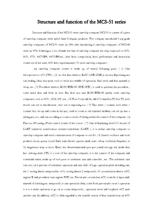
Structure and function of the MCS-51 seriesStructure and function of the MCS-51 series one-chip computer MCS-51 is a name of a piece of one-chip computer series which Intel Company produces. This company introduced 8 top-grade one-chip computers of MCS-51 series in 1980 after introducing 8 one-chip computers of MCS-48 series in 1976. It belong to a lot of kinds this line of one-chip computer the chips have,such as 8051, 8031, 8751, 80C51BH, 80C31BH,etc., their basic composition, basic performance and instruction system are all the same. 8051 daily representatives- 51 serial one-chip computers .An one-chip computer system is made up of several following parts: ( 1) One microprocessor of 8 (CPU). ( 2) At slice data memory RAM (128B/256B),it use not depositting not can reading /data that write, such as result not middle of operation, final result and data wanted to show, etc. ( 3) Procedure memory ROM/EPROM (4KB/8KB ), is used to preserve the procedure , some initial data and form in slice. But does not take ROM/EPROM within some one-chip computers, such as 8031 , 8032, 80C ,etc.. ( 4) Four 8 run side by side I/O interface P0 four P3, each mouth can use as introduction , may use as exporting too. ( 5) Two timer / counter, each timer / counter may set up and count in the way, used to count to the external incident, can set up into a timing way too, and can according to count or result of timing realize the control of the computer. ( 6) Five cut off cutting off the control system of the source . ( 7) One all duplexing serial I/O mouth of UART (universal asynchronous receiver/transmitter (UART) ), is it realize one-chip computer or one-chip computer and serial communication of computer to use for. ( 8) Stretch oscillator and clock produce circuit, quartz crystal finely tune electric capacity need outer. Allow oscillation frequency as 12 megahertas now at most. Every the above-mentioned part was joined through the inside data bus .Among them, CPU is a core of the one-chip computer, it is the control of the computer and command centre, made up of such parts as arithmetic unit and controller , etc.. The arithmetic unit can carry on 8 persons of arithmetic operation and unit ALU of logic operation while including one, the 1 storing device temporarilies of 8, storing device 2 temporarily, 8's accumulation device ACC, register B and procedure state register PSW, etc. Person who accumulate ACC count by 2 input ends entered of checking etc. temporarily as one operation often, come from person who store 1 operation is it is it make operation to go on to count temporarily , operation result and loopback ACC with another one. In addition, ACC is often regarded as the transfer station of data transmission on 8051inside . The same as general microprocessor, it is the busiest register. Help remembering that agreeing with A expresses in the order. The controller includes the procedure counter , the order is depositted, the order decipher, the oscillator and timing circuit, etc. The procedure counter is made up of counter of 8 for two, amounts to 16. It is a byte address counter of the procedure in fact, the content is the next IA that will carried out in PC. The content which changes it can change the direction that the procedure carries out . Shake the circuit in 8051 one-chip computers, only need outer quartz crystal and frequency to finely tune the electric capacity, its frequency range is its 12MHZ of . This pulse signal, as 8051 basic beats of working, namely the minimum unit of time. 8051 is the same as other computers, the work in harmony under the control of the basic beat, just like an orchestra according to the beat play that is commanded.There are ROM (procedure memory , can only read ) and RAM in 8051 slices (data memory, can is it can write ) two to read, they have each independent memory address space, dispose way to be the same with general memory of computer. Procedure 8051 memory and 8751 slice procedure memory capacity 4KB, address begin from 0000H, used for preserving the procedure and form constant. Data 8051- 8751 8031 of memory data memory 128B, address false 00FH, use for middle result to deposit operation, the data are stored temporarily and the data are buffered etc.. In RAM of this 128B, there is unit of 32 byteses that can be appointed as the job register, this and general microprocessor is different, 8051 slice RAM and job register rank one formation the same to arrange the location. It is not very the same that the memory of MCS-51 series one-chip computer and general computer disposes the way in addition. General computer for first address space, ROM and RAM can arrange in different space within the range of this address at will, namely the addresses of ROM and RAM, with distributing different address space in a formation. While visiting the memory, corresponding and only an address Memory unit, can ROM, it can be RAM too, and by visiting the order similarly. This kind of memory structure is called the structure of Princeton. 8051 memories are divided into procedure memory space and data memory space on the physics structure, there are four memory spaces in all: The procedure stores in one and data memory space outside data memory and one in procedure memory space and one outside one, the structure forms of this kind of procedure device and data memory separated form data memory, called Harvard structure. But use the angle from users, 8051 memory address space is divided into three kinds: (1) In the slice, arrange blocks of FFFFH , 0000H of location , in unison outside the slice (use 16 addresses). (2) The data memoryaddress space outside one of 64KB, the address is arranged from 0000H 64KB FFFFH (with 16 addresses ) too to the location. (3) Data memory address space of 256B (use 8 addresses). Three above-mentioned memory space addresses overlap, for distinguishing and designing the order symbol of different data transmission in the instruction system of 8051: CPU visit slice, ROM order spend MOVC , visit block RAM order uses MOVX outside the slice, RAM order uses MOV to visit in slice.8051 one-chip computer have four 8 walk abreast I/O port, call P0, P1, P2 and P3. Each port is 8 accurate two-way mouths, accounts for 32 pins altogether. Every one I/O line can be used as introduction and exported independently. Each port includes a latch (namely special function register ), one exports the driver and a introduction buffer . Make data can latch when outputting, data can buffer when making introduction , but four function of passway these self-same. Expand among the system of memory outside having slice, four port these may serve as accurate two-way mouth of I/O in common use. Expand among the system of memory outside having slice, P2 mouth see high 8 address off; P0 mouth is a two-way bus, send the introduction of 8 low addresses and data / export in timesharingOutput grade , P3 of mouth , P1 of P1 , connect with inside have load resistance of drawing , every one of they can drive 4 Model LS TTL load to output. As while inputting the mouth, any TTL or NMOS circuit can drive P1 of 8051 one-chip computers as P3 mouth in a normal way . Because draw resistance on output grade of them have, can open a way collector too or drain-source resistance is it urge to open a way, do not need to have the resistance of drawing outerly . Mouths are all accurate two-way mouths too. When the conduct is input, must write the corresponding port latch with 1 first . As to 80C51 one-chip computer, port can only offer milliampere of output electric currents, is it output mouth go when urging one ordinary basing of transistor to regard as, should contact a resistance among the port and transistor base , in order to the electricity while restraining the high level from exporting P1~P3 Being restored to the throne is the operation of initializing of an one-chip computer. Its main function is to turn PC into 0000H initially , make the one-chip computer begin to hold the conduct procedure from unit 0000H. Except that the ones that enter the system are initialized normally,as because procedure operate it make mistakes or operate there aren't mistake, in order to extricate oneself from a predicament , need to be pressed and restored to the throne the key restarting too. It is an input end which is restored to the throne the signal in 8051 China RST pin. Restore to the throne signal high level effective , should sustain 24 shake cycle (namely 2 machinecycles ) the above its effective times. If 6 of frequency of utilization brilliant to shake, restore to the throne signal duration should exceed 4 delicate to finish restoring to the throne and operating. Produce the logic picture of circuit which is restored to the throne the signal:Restore to the throne the circuit and include two parts outside in the chip entirely. Outside that circuit produce to restore to the throne signal (RST ) hand over to Schmitt's trigger, restore to the throne circuit sample to output , Schmitt of trigger constantly in each S5P2 , machine of cycle in having one more , then just got and restored to the throne and operated the necessary signal insidly. Restore to the throne resistance of circuit generally, electric capacity parameter suitable for 6 brilliant to shake, can is it restore to the throne signal high level duration greater than 2 machine cycles to guarantee. Being restored to the throne in the circuit is simple, its function is very important. Pieces of one-chip computer system could normal running,should first check it can restore to the throne not succeeding. Checking and can pop one's head and monitor the pin with the oscillograph tentatively, push and is restored to the throne the key, the wave form that observes and has enough range is exported (instantaneous), can also through is it restore to the throne circuit group holding value carry on the experiment to change.At present,MCU to infiltrate all areas of our lives, which is almost difficult to find traces of the field without SCM. Missile navigation equipment, aircraft, all types of instrument control, computer network communications and data transmission, industrial automation, real-time process control and data processing, extensive use of various smart IC card, civilian luxury car security system, video recorder, camera, fully automatic washing machine control, and program-controlled toys, electronic pet, etc., which are inseparable from the microcontroller. Not to mention the area of robot control, intelligent instruments, medical equipment was. Therefore, the MCU learning, development and application of the large number of computer applications and intelligent control of the scientists, engineers.SCM is widely used in instruments and meters, household appliances, medical equipment, aerospace, specialized equipment, intelligent management and process control fields, roughly divided into the following several areas:(1)In the application of Intelligent InstrumentsSCM has a small size, low power consumption, controlling function, expansion flexibility, the advantages of miniaturization and ease of use, widely used instrument, combining different types ofsensors can be realized Zhuru voltage, power, frequency, humidity, temperature, flow, speed, thickness, angle, length, hardness, elemental, physical pressure measurement. SCM makes use of digital instruments, intelligence, miniaturization, and functionality than electronic or digital circuits more powerful. Such as precision measuring equipment (power meter, oscilloscope, various analytical instrument).(2)In the industrial control applicationWith the MCU can constitute a variety of control systems, data acquisition system. Such as factory assembly line of intelligent control,all kinds of alarm systems,and computer networks constitute a secondary control system.(3)In the Appliance of Household appliancesIt can be said that the appliances are basically using SCM, praise from the electric rice, washing machines, refrigerators, air conditioners, color TV, and other audio video equipment, to the electronic weighing equipment, varied, and omnipresent.(4)In the field of computer networks and communications applicationsMCU general with modern communication interface, can be easy with the computer data communication, networking and communications in computer applications between devices had excellent material conditions, are basically all communication equipment to achieve a controlled by MCU from mobile phone, telephone, mini-program-controlled switchboards, building automated communications call system, train radio communication, to the daily work can be seen everywhere in the mobile phones, trunked mobile radio, walkie-talkies, etc..(5)Microcomputer in the field of medical device applicationsMCU in the use of medical devices is also quite extensive, such as medical respirator, the various analyzers, monitors, ultrasound diagnostic equipment and hospital beds, etc. call system.(6)In a variety of major appliances in the modular applicationsDesigned to achieve some special single specific function to be modular in a variety of circuit applications, without requiring the use of personnel to understand its internal structure. If music integrated single chip, seemingly simple function, miniature electronic chip in the net (the principle is different from the tape machine), you need a computer similar to the principle of the complex. Such as: music signal to digital form stored in memory (like ROM), read by the microcontroller, analog music into electrical signals (similar to the sound card).In large circuits, modular applications that greatly reduce the volume, simplifies the circuit and reduce the damage, error rate, but also easy to replace.(7)Microcontroller in the application field of automotive equipmentSCM in automotive electronics is widely used, such as a vehicle engine controller, CAN bus-based Intelligent Electronic Control Engine, GPS navigation system, abs anti-lock braking system, brake system, etc..In addition, the MCU in business, finance, research, education, national defense, aerospace and other fields has a very wide range of applications.51系列单片机的结构和功能51系列单片机是英特尔公司生产的具有必然结构和功能的单片机产品。
单片机【经典外文翻译】--单片机基础(译文+英文)—-毕业论文设计
Fundamentals of Single-chip MicrocomputerTh e si ng le-ch i p mi cr oc om pu ter is t he c ul mi nat i on o f bo th t h e d ev el op me nt o f th e d ig it al com p ut er an d t he int e gr at ed ci rc ui ta r gu ab ly th e t ow m os t s i gn if ic ant i nv en ti on s o f t h e 20t h c en tury[1].Th es e to w typ e s of a rc hi te ctu r e ar e fo un d i n s in gl e-ch ip m i cr oc om pu te r. So m e em pl oy t he sp l it p ro gr am/d ata me mo ry o f th e H a rv ar d ar ch it ect u re, sh ow n in Fi g.3-5A-1, o th ers fo ll ow t hep h il os op hy, wi del y a da pt ed f or ge n er al-p ur po se co m pu te rs a ndm i cr op ro ce ss or s, of ma ki ng no lo gi c al di st in ct io n be tw ee n p ro gram a n d da ta m em or y a s i n th e Pr in cet o n ar ch it ec tu re,sh ow n inF i g.3-5A-2.In g en er al te r ms a s in gl e-chi p m ic ro co mp ut er i sc h ar ac te ri zed b y the i nc or po ra tio n of al l t he uni t s o f a co mp ut er i n to a s in gl e dev i ce, as s ho w n in Fi g3-5A-3.Fig.3-5A-1 A Harvard typeFig.3-5A-2. A conventional Princeton computerFig3-5A-3. Principal features of a microcomputerRead only memory (ROM).R OM i s u su al ly f or th e p er ma ne nt,n o n-vo la ti le s tor a ge o f an a pp lic a ti on s pr og ra m .M an ym i cr oc om pu te rs an d mi cr oc on tr ol le r s a re in t en de d fo r h ig h-v olume a p pl ic at io ns a nd h en ce t he e co nom i ca l ma nu fa ct ure of t he d ev ic es r e qu ir es t ha t the co nt en ts o f the pr og ra m me mo ry b e co mm it te dp e rm an en tl y d ur in g th e m an uf ac tu re o f c hi ps . Cl ear l y, th is im pl iesa ri g or ou s a pp roa c h t o R OM co de d e ve lo pm en t s in ce c ha ng es ca nnotb e m ad e af te r man u f a ct ur e .T hi s d e ve lo pm en t pr oce s s ma y in vo lv e e m ul at io n us in g a s op hi st ic at ed deve lo pm en t sy st em w i th a ha rd wa re e m ul at io n ca pa bil i ty a s we ll a s th e u se of po we rf ul so ft wa re t oo ls.So me m an uf act u re rs p ro vi de ad d it io na l RO M opt i on s byi n cl ud in g i n th ei r r a ng e de vi ce s wi th (or i nt en de d fo r us e with) u s er pr og ra mm ab le m em or y. Th e s im p le st of th es e i s us ua ll y d evice w h ic h ca n op er ate in a m ic ro pr oce s so r mo de b y usi n g so me o f th e i n pu t/ou tp ut li ne s as a n ad dr es s an d da ta b us f or acc e ss in g e xt er na l m e mo ry. T hi s t ype o f d ev ic e c an b e ha ve fu nc ti on al l y a s t he si ng le c h ip mi cr oc om pu te r fr om wh ic h i t i s de ri ve d a lb eit w it h r es tr ic ted I/O an d a mo di fie d e xt er na l ci rcu i t. T he u se o f t h es e RO Ml es sd e vi ce s is c om mo n e ve n in p ro du ct io n c ir cu it s wh er e t he v ol um e does n o t j u st if y th e d e ve lo pm en t co sts of c us to m on-ch i p RO M[2];t he re c a n st il l b e a si g ni fi ca nt s a vi ng in I/O a nd ot he r c hi ps co mp ared t o a c on ve nt io nal mi cr op ro ce ss or b as ed c ir cu it. M o re e xa ctr e pl ac em en t fo r RO M d ev ic es c an b e o bt ai ne d in t he f o rm o f va ri antsw i th 'pi gg y-ba ck'EP RO M(Er as ab le p ro gr am ma bl e ROM)s oc ke ts o rd e vi ce s w it h EP ROM i ns te ad o f R OM 。
单片机设计外文翻译
附录A英文原文1The SerialPort Interface of the LCD Driver ICThis section will describe how to control the register value of the LCD driver IC on the LTM.The LCD and touch panel module on the LTM is equipped with a LCD driver IC to support three display resolution and with functions of source driver, serial port interface, timing controller, and power supply circuits. To control these functions, users can use FPGA to configure the registers in the LCD driver IC via serial port interface.Also, there is an analog to digital converter (ADC) on the LTM to convert the analog X/Y coordinates of the touch point to digital data and output to FPGA through the serial port interface of the ADC.Both LCD driver IC and ADC serial port interfaces are connected to the FPGA via the 40-pin expansion header and IDE cable.Because of the limited number of I/O on the expansion header, the serial interfaces of the LCD driver IC and ADC need to share the same clock (ADC_DCLK) and chip enable (SCEN)signal I/O on the expansion header. To avoid both the serial port interfaces may interfere with each other when sharing the same clock and chip enable signals, the chip enable signal (CS), which is inputted into the ADC will come up with a logicinverter as shown in Figure1.1.Figure 1.1 The serial interface of the LCD touch panel module and AD7843Users need to pay attention controlling the shared signals when designing the serial portinterface controller. The detailed register maps of the LCD driver IC are listed in appendix chapter.The specifications of the serial port interface of the LCD driver IC are described below.The LCD driver IC supports a clock synchronous serial interface as the interface to a FPGA toenable instruction setting. Please notice that in addition to the serial port interface signals, NCLKinput should also be provided while setting the registers. Figure 1.2 and Table1.1 show the frameformat and timing diagram of the serial port interface. The LCD driver IC recognizes the start of datatransfer on the falling edge of SCEN input and starts data transfer. When setting instruction, theTPG110 inputs the setting values via SDA on the rising edge of input SCL.Table 1.1 The timing parameters of the serial port interfaceThe first 6 bits (A5 ~ A0) specify the address of the register. The next bit means Read/Writecommand. “0” is write command. “1” is read command. Then, the next cycle is turn-round cycle.Finally, the last 8 bits are for Data setting (D7 ~ D0). The address and data are transferred from theMSB to LSB sequentially. The data is written to the register of assigned address when “End oftransfer” is detected after the 16th SCL rising cycles. Data is not accepted if there are less or morethan 16 cycles for one transaction.Figure 1.2 The frame format and timing diagram of the serial port interface2Input timing of the LCD panel display functionThis section will describe the timing specification of the LCD synchronous signals and RGB data.To determine the sequencing and the timing of the image signals displayed on the LCD panel, the corresponding synchronous signals from FPGA to the LCD panel should follow the timing specification.Figure 2.1LCD horizontal timing specificationFigure 2.1 illustrates the basic timing requirements for each row (horizontal) that is displayed on the LCD panel. An active-low pulse of specific duration (time t hpw inthe figure) is applied to the horizontal synchronization (HD) input of the LCD panel, which signifies the end of one row of data and the start of the next. The data (RGB) inputs on the LCD panel are not valid for a time period called the hsync back porch ( t hbp) after the hsync pulse occurs, which is followed by the display area ( t hd). During the data display area the RGB data drives each pixel in turn across the row being displayed. Also, during the period of the data display area, the data enable signal (DEN) must be driven to logic high. Finally, there is a time period called the hsync front porch ( t hfp ) where the RGB signals are not valid again before the next hsync pulse can occur.The timing of the vertical synchronization (VD) is the same as shown in Figure 2.2, except that a vsync pulse signifies the end of one frame and the start of the next, and the data refers to the set of rows in the frame (horizontal timing). Table 2.1 and 2.2 show for different resolutions, the durations of time periods t hpw ,t hbp , t hd , and t hfp for both horizontal and vertical timing. Finally, the timing specification of the synchronous signals is shown in the Table2.3.Table 2.1 LCD horizontal timing parametersFigure 2.2 LCD vertical timing specificationTable 2.3 The timing parameters of the LCD synchronous signals3The serial interface of the AD converterThis section will describe how to obtain the X/Y coordinates of the touch point from the AD converter.The LTM also equipped with an Analog Devices AD7843 touch screen digitizer chip. The AD7843 is a12-bit analog to digital converter (ADC) for digitizing x and y coordinates of touch points applied to the touchscreen. The coordinates of the touch point stored in the AD7843 can be obtained by the serial port interface.To obtain the coordinate from the ADC, the first thing users need to do is monitor the interrupt signalADC_PENIRQ_n outputted from the ADC. By connecting a pull high resistor, the ADC_PENIRQ_n outputremains high normally. When the touch screen connected to the ADC is touched via a pen or finger, theADC_PENIRQ_n output goes low, initiating an interrupt to a FPGA that can theninstruct a control word to bewritten to the ADC via the serial port interface.The control word provided to the ADC via the DIN pin is shown in Figure3.1. This provides the conversionstart, channel addressing, ADC conversion resolution, configuration, and power-down of the ADC. Thedetailed information on the order and description of these control bits can be found from the datasheet of theADC in the DATASHEET folder on the LTM System CD-ROM.Figure 3.1 Control register bit function descriptionFigure 3.2 shows the typical operation of the serial interface of the ADC. The serial clock provides theconversion clock and also controls the transfer of information to and from the ADC. One complete conversioncan be achieved with 24 ADC_DCLK cycles. The detailed behavior of the serial port interface can be found inthe datasheetof the ADC. Note that the clock (ADC_DCLK) and chip enable signals (SCEN) of the serial portinterface SHRAE the same signal I/O with LCD driver IC. Users should avoid controlling the LCD driver ICand ADC at the same time when designing the serial port interface controller. Also, because the chip enablesignal (SCEN) inputted to the ADC comes up with a logic inverter, the logic level of the SCEN should beinverse when it is used to control the ADC.Figure 3.2 Conversion timing of the serial port interface4 Block Diagram of the Ephoto DesignThis section will describe the block diagram of the Ephoto demonstration tohelp users in reading the code provided.Figure 4.1 shows the block diagram of the EPhoto demonstration. As soon as the bit stream is downloaded into the FPGA, the register values of the LCD driver IC using to control the LCD display function will be configured by the LCD_SPI_Controllerblock, which uses the serial port interface to communicate with the LCD driver IC. Meanwhile, the Flash_to_SDRAM_Controllerblock will read the RGB data of one picture stored in the Flash, and then write the data into SDRAM buffer. Accordingly, both the synchronous control signals and the picture data stored in the SDRAM buffer will be sent to the LTM via the LCD_Timing_Controllerblock.When users touch LTM screens, the x and y coordinates of the touch point will be obtained by the ADC_SPI_Controllerblock through the ADC serial port interface.Then the Touch_Point_Detectorblock will determine whether these coordinates are in a specific range. If the coordinates fit the range, the Touch_Point_Detectorblock will control the Flash_to_SDRAM_Controllerblock to read the next or previous picture's data from the Flash and repeat the steps as mentioned before to command the LTM to display the next or previous picture.Figure 4.1The block diagram of the Ephoto demonstration4SDRAM Controller Simulation ModelThe SDRAM controller design files generated by SOPC Builder are suitable for both synthesis and simulation. Some simulation features are implemented in the HDL using “translate on/off” synthesis directives that make certain sections of HDL code invisible to the synthesis tool. The simulation features are implemented primarily for easy simulation of Nios and Nios II processor systems using the ModelSimsimulator. The SDRAM controller simulation model is not ModelSim specific. However, minor changes may be required to make the model work with other simulators.If you changethe simulation directives to create a custom simulation flow, be aware that SOPC Builder overwrites existing files during system generation. Take precautions to ensure your changes are not overwritten.Simulating Nios II Processor Designsfor a demonstration of simulation of the SDRAM controller in the context of Nios II embedded processor systems.5SDRAM Memory ModelThis section describes the two options for simulating a memory model of the SDRAMchip.6.1Using the Generic Memory ModelIf the Include a functional memory model the system testbenchoption is enabled at system generation, SOPC Builder generates an HDL simulation model for the SDRAM memory. In the auto-generated system testbench, SOPC Builder automatically wires this memory model to the SDRAM controller pins. Using the automatic memory model and testbench accelerates the process of creating and verifying systems that use the SDRAM controller. However, the memory model is a generic functional model that does not reflect the true timing or functionality of real SDRAM chips. The generic model is always structured as a single, monolithic block of memory. For example, even for a system that combines two SDRAM chips, the generic memory model is implemented as a single entity.6.2 Using the SDRAM Manufacturer’s Memory ModelIf the Include a functional memory model the system testbenchoption is not enabled, you are responsible for obtaining a memory model from the SDRAM manufacturer, and manually wiring the model to the SDRAM controller pins in the system testbench.The following examples show how to connect the SDRAM controller outputs to an SDRAM chip or chips. The bus labeled ctl is an aggregate of the remaining signals, such as cas_n, ras_n, cke and we_n. Figure 6.1shows a single 128-Mbit SDRAM chipwith 32-bit data. The address, data, and control signals are wired directly from the controller to the chip. The result is a 128-Mbit (16-Mbyte) memory space.Figure 6.2shows two 64-Mbit SDRAM chips, each with 16-bit data. The address and control signals connect in parallel to both chips. The chips share the chipselect (cs_n) signal. Each chip provides half of the 32-bit data bus. The result is a logical 128-Mbit (16-Mbyte) 32-bit data memory.Figure 6.1Single 128-Mbit SDRAM Chip with 32-Bit DataFigure 6.2Two 64-MBit SDRAM Chips Each with 16-Bit Data Figure 6.3 shows two 128-Mbit SDRAM chips, each with 32-bit data. The address, data, and control signals connect in parallel to the two chips. The chipselect bus (cs_n[1:0]) determines which chip is selected. The result is a logical 256-Mbit 32-bit wide memory.Figure 6.3.Two 128-Mbit SDRAM Chips Each with 32-Bit Data6.3Software Programming ModelThe SDRAM controller behaves like simple memory when accessed via the Avalon-MM interface. There are no software-configurable settings and no memory-mapped registers. No software driver routines are required for a processor to access the SDRAM controller.Clock, PLL and Timing ConsiderationsThis section describes issues related to synchronizing signals from the SDRAMcontroller core with the clock that drives the SDRAM chip. During SDRAMtransactions, the address, data, and control signals are valid at the SDRAM pins for awindow of time, during which the SDRAM clock must toggle to capture the correctvalues. At slower clock frequencies, the clock naturally falls within the valid window.At higher frequencies, you must compensate the SDRAM clock to align with the validwindow.Determine when the valid window occurs either by calculation or by analyzing theSDRAM pins with an oscilloscope. Then use a PLL to adjust the phase of theSDRAMclock so that edges occur in the middle of the valid window. Tuning the PLL mightrequire trial-and-error effort to align the phase shift to the properties of your targetboard. For details about the PLL circuitry in your target device, refer to the appropriatedevice family handbook. For details about configuring the PLLs in Altera devices,refer to the ALTPLL Megafunction User Guide.6.4Factors Affecting SDRAM TimingThe location and duration of the window depends on several factors:(1) Timing parameters of the device and SDRAM I/O pins —I/O timingparameters vary based on device family and speed grade.(2)Pin location on the device — I/O pins connected to row routing have differenttiming than pins connected to column routing.(3)Logic options used during the Quartus II compilation — Logic options suchas the Fast Input Registerand Fast Output Registerlogic affect the design fit.The location of logic and registers inside the device affects the propagation delays of signals to the I/O pins.(4) SDRAM CAS latencyAs a result, the valid window timing is different for different combinations of FPGA and SDRAM devices. The window depends on the Quartus II software fitting results and pin assignments.6.5Symptoms of an Untuned PLLDetecting when the PLL is not tuned correctly might be difficult. Data transfers to or from the SDRAM might not fail universally. For example, individual transfers to the SDRAM controller might succeed, whereas burst transfers fail. For processor-based systems, if software can perform read or write data to SDRAM, but cannot run when the code is located in SDRAM, the PLL is probably tuned incorrectly.6.6Estimating the Valid Signal WindowThis section describes how to estimate the location and duration of the valid signal window using timing parameters provided in the SDRAM datasheet and the Quartus II software compilation report. After finding the window, tune the PLL so that SDRAM clock edges occur exactly in the middle of the window. Calculating the window is a two-step process. First, determine by how much time the SDRAM clock can lag the controller clock, and then by how much time it can lead. After finding the maximum lag and lead values, calculate the midpoint between them.These calculations provide an estimation only. The following delays can also affect proper PLL tuning, but are not accounted for by these calculations.(1)Signal skew due to delays on the printed circuit board — These calculations assume zero skew.(2)Delay from the PLL clock output nodes to destinations — These calculations assume that the delay from the PLL SDRAM-clock output-node to the pin is the same as the delay from the PLL controller-clock output-node to the clock inputs in the SDRAM controller. If these clock delays are significantly different, you must account for this phase shift in your window calculations.附录 B 中文翻译1从串行端口LCD的接口驱动IC本节将介绍如何控制在LTM上的LCD驱动IC的寄存器值,LCD和触摸屏模块的LTM配备了LCD驱动IC支持三中显示分辨率以及源驱动器、串行接口、时序控制器、电源电路的功能。
单片机毕业设计(论文)外文资料翻译---51系列单片机的结构和功能

毕业设计(论文)外文资料翻译系:电光系专业:电子科学与技术姓名:学号: 080403136外文出处:Structure and function of(用外文写)the MCS-51 series 附件: 1.外文资料翻译译文;2.外文原文。
指导教师评语:签名:年月日注:请将该封面与附件装订成册。
附件1:外文资料翻译译文51系列单片机的结构和功能51系列单片机是英特尔公司生产的具有一定结构和功能的单片机产品。
这家公司在1976年引入8位MCS - 48系列单片机后,于1980年又推出了8位高档的MCS - 51系列单片机。
它包含很多种这类型的单片机,如8051,8031,8751,80C51BH,80C31BH等,它们的基本组成,基本性能和指令系统都是一样的。
一般情况习惯用8051来代表51系列单片机。
早期的单片机都是8位或4位的。
其中最成功的是INTEL的8031,因为简单可靠而性能不错获得了很大的好评。
此后在8031上发展出了MCS51系列单片机系统。
基于这一系统的单片机系统直到现在还在广泛使用。
随着工业控制领域要求的提高,开始出现了16位单片机,但因为性价比不理想并未得到很广泛的应用。
90年代后随着消费电子产品大发展,单片机技术得到了巨大提高。
随着INTEL i960系列特别是后来的ARM系列的广泛应用,32位单片机迅速取代16位单片机的高端地位,并且进入主流市场。
而传统的8位单片机的性能也得到了飞速提高,处理能力比起80年代提高了数百倍。
目前,高端的32位单片机主频已经超过300MHz,性能直追90年代中期的专用处理器,而普通的型号出厂价格跌落至1美元,最高端的型号也只有10美元。
当代单片机系统已经不再只在裸机环境下开发和使用,大量专用的嵌入式操作系统被广泛应用在全系列的单片机上。
而在作为掌上电脑和手机核心处理的高端单片机甚至可以直接使用专用的Windows和Linux操作系统。
单片机比专用处理器更适合应用于嵌入式系统,因此它得到了最多的应用。
单片机的外文文献及中文翻译

单片机的外文文献及中文翻译一、外文文献Title: The Application and Development of SingleChip Microcontrollers in Modern ElectronicsSinglechip microcontrollers have become an indispensable part of modern electronic systems They are small, yet powerful integrated circuits that combine a microprocessor core, memory, and input/output peripherals on a single chip These devices offer significant advantages in terms of cost, size, and power consumption, making them ideal for a wide range of applicationsThe history of singlechip microcontrollers can be traced back to the 1970s when the first microcontrollers were developed Since then, they have undergone significant advancements in technology and performance Today, singlechip microcontrollers are available in a wide variety of architectures and capabilities, ranging from simple 8-bit devices to complex 32-bit and 64-bit systemsOne of the key features of singlechip microcontrollers is their programmability They can be programmed using various languages such as C, Assembly, and Python This flexibility allows developers to customize the functionality of the microcontroller to meet the specific requirements of their applications For example, in embedded systems for automotive, industrial control, and consumer electronics, singlechip microcontrollers can be programmed to control sensors, actuators, and communication interfacesAnother important aspect of singlechip microcontrollers is their low power consumption This is crucial in batterypowered devices and portable electronics where energy efficiency is of paramount importance Modern singlechip microcontrollers incorporate advanced power management techniques to minimize power consumption while maintaining optimal performanceIn addition to their use in traditional electronics, singlechip microcontrollers are also playing a significant role in the emerging fields of the Internet of Things (IoT) and wearable technology In IoT applications, they can be used to collect and process data from various sensors and communicate it wirelessly to a central server Wearable devices such as smartwatches and fitness trackers rely on singlechip microcontrollers to monitor vital signs and perform other functionsHowever, the design and development of systems using singlechip microcontrollers also present certain challenges Issues such as realtime performance, memory management, and software reliability need to be carefully addressed to ensure the successful implementation of the applications Moreover, the rapid evolution of technology requires developers to constantly update their knowledge and skills to keep up with the latest advancements in singlechip microcontroller technologyIn conclusion, singlechip microcontrollers have revolutionized the field of electronics and continue to play a vital role in driving technological innovation Their versatility, low cost, and small form factor make them an attractive choice for a wide range of applications, and their importance is expected to grow further in the years to come二、中文翻译标题:单片机在现代电子领域的应用与发展单片机已成为现代电子系统中不可或缺的一部分。
at89c52单片机中英文资料对照外文翻译文献综述
D.htmlat89c52单片机中英文资料对照外文翻译文献综述at89c52单片机简介中英文资料对照外文翻译文献综述AT89C52 Single-chip microprocessor introductionSelection of Single-chip microprocessor1. Development of Single-chip microprocessorThe main component part of Single-chip microprocessor as a result of by such centralize to be living to obtain on the chip,In immediate future middle processor CPU。
Storage RAM immediately﹑memoy readROM﹑Interrupt system、Timer /'s counter along with I/O's rim electric circuit awaits the main microcomputer section,The lumping is living on the chip。
Although the Single-chip microprocessor r is only a chip,Yet through makes up and the meritorous service be able to on sees,It had haveed the calculating machine system property,calling it for this reason act as Single-chip microprocessor r minisize calculating machine SCMS and abbreviate the Single-chip microprocessor。
- 1、下载文档前请自行甄别文档内容的完整性,平台不提供额外的编辑、内容补充、找答案等附加服务。
- 2、"仅部分预览"的文档,不可在线预览部分如存在完整性等问题,可反馈申请退款(可完整预览的文档不适用该条件!)。
- 3、如文档侵犯您的权益,请联系客服反馈,我们会尽快为您处理(人工客服工作时间:9:00-18:30)。
附录I参考文献及译文英文资料AT89S51(8-bit Micro controller with 4K Bytes Flash)The AT89S51 is a low-power, high-performance CMOS 8-bit microcontroller with 4K bytes of In-System Programmable Flash memory. The device is manufactured using Atmel's high-density nonvolatile memory technology and is compatible with the industry-standard 80C51 instruction set and pinout. The on-chip Flash allows the program memory to be reprogrammed in-system or by a conventional nonvolatile memory programmer. By combining a versatile 8-bit CPU with In-System Programmable Flash on a monolithic chip, the Atmel AT89S51 is a powerful microcontroller which provides a highly-flexible and cost-effective solution to many embedded control applications.Features:Compatible with MCS.-51 Products4K Bytes of In-System Programmable (ISP) Flash MemoryEndurance: 1000 Write/Erase Cycles4.0V to5.5V Operating RangeFully Static Operation: 0 Hz to 33 MHzThree-level Program Memory Lock128 x 8-bit Internal RAM32 Programmable I/O LinesTwo 16-bit Timer/CountersSix Interrupt SourcesFull Duplex UART Serial ChannelLow-power Idle and Power-down ModesInterrupt Recovery from Power-down ModeWatchdog TimerDual Data PointerPower-off FlagFast Programming TimeFlexible ISP Programming (Byte and Page Mode)Green (Pb/Halide-free) Packaging OptionThe AT89S51 provides the following standard features: 4K bytes of Flash, 128 bytes of RAM, 32 I/O lines, Watchdog timer, two data pointers, two 16-bit timer/counters, a five-vector two-level interrupt architecture, a full duplex serial port, on-chip oscillator, and clock circuitry. In addition, the AT89S51 is designed with static logic for operation down to zero frequency and supports two software selectable power saving modes. The Idle Mode stops the CPU while allowing the RAM, timer/counters, serial port, and interrupt system to continue functioning. The Power-down mode saves the RAM contents but freezes the oscillator, disabling all other chip functions until the next external interrupt or hardware reset.VCC:Supply voltage (all packages except 42-PDIP).GND:Ground (all packages except 42-PDIP; for 42-PDIP GND connects only the logic core and the embedded program memory).VDD:Supply voltage for the 42-PDIP which connects only the logic core and the embedded program memory.PWRVDD:Supply voltage for the 42-PDIP which connects only the I/O Pad Drivers. The application board MUST connect both VDD and PWRVDD to the board supply voltage.PWRGND:Ground for the 42-PDIP which connects only the I/O Pad Drivers. PWRGND and GND are weakly connected through the common silicon substrate, but not through any metal link. The application board MUST connect both GND and PWRGND tothe board ground.Port 0:Port 0 is an 8-bit open drain bi-directional I/O port. As an output port, each pin can sink eight TTL inputs. When 1s are written to port 0 pins, the pins can be used as high-impedance inputs.Port 0 can also be configured to be the multiplexed low-order address/data bus during accesses to external program and data memory. In this mode, PO has internal pull-ups.Port 0 also receives the code bytes during Flash programming and outputs the code bytes during program verification. External pull-ups are required during program verification.Port 1:Port 1 is an 8-bit bi-directional I/O port with internal pull-ups. The Port 1 output buffers can sink/source four TTL inputs. When 1s are written to Port 1 pins, they are pulled high by the internal pull-ups and can be used as inputs. As inputs, Port 1 pins that are externally being pulled low will source current (lip) because of the internal pull-ups.Port 2:Port 2 is an 8-bit bi-directional I/O port with internal pull-ups. The Port 2 output buffers can sink/source four TTL inputs. When 1s are written to Port 2 pins, they are pulled high by the internal pull-ups and can be used as inputs. As inputs, Port 2 pins that are externally being pulled low will source current (lip) because of the internal pull-ups.Port 2 emits the high-order address byte during fetches from external program memory and during accesses to external data memory that uses 16-bit addresses (MOVX@DPTR). In this application, Port 2 uses strong internal pull-ups when emitting 1s. During accesses to external data memory that use 8-bit addresses (MOVX@RI), Port 2 emits the contents of the P2 Special Function Register.Port 2 also receives the high-order address bits and some control signals duringFlash programming and verification.Port 3:Port 3 is an 8-bit bi-directional I/O port with internal pull-ups. The Port 3 output buffers can sink/source four TTL inputs. When 1s are written to Port 3 pins, they are pulled high by the internal pull-ups and can be used as inputs. As inputs, Port 3 pins that are externally being pulled low will source current (lip) because of the pull-ups.Port 3 receives some control signals for Flash programming and verification.Port 3 also serves the functions of various special features of the AT89S51,as shown in the following table.RST:Reset input. A high on this pin for two machine cycles while the oscillator is running resets the device. This pin drives High for 98 oscillator periods after the Watchdog times out. The DISRTO bit in SFR AUXR (address 8EH) can be used to disable this feature. In the default state of bit DISRTO, the RESET HIGH out feature is enabled.ALE/PROG:Address Latch Enable (ALE) is an output pulse for latching the low byte of the address during accesses to external memory. This pin is also the program pulse input (PROG) during Flash programming. In normal operation, ALE is emitted at a constant rate of 1/6 the oscillator frequency and may be used for external timing or clocking purposes. Note, however, that one ALE pulse is skipped during each access to external data memory.If desired, ALE operation can be disabled by setting bit 0 of SFR location 8EH. With the bit set, ALE is active only during a MOVX or MOVC instruction. Otherwise, the pin is weakly pulled high. Setting the ALE-disable bit has no effect if the microcontroller is in external execution mode.PSEN:Program Store Enable (PSEN) is the read strobe to external program memory.When the AT89S51 is executing code from external program memory, PSEN is activated twice each machine cycle, except that two PSEN activations are skipped during each access to external data memory.EA/VPP:External Access Enable. EA must be strapped to GND in order to enable the device to fetch code from external program memory locations starting at OOOOH up to FFFFH. Note, however, that if lock bit 1 is programmed, EA will be internally latched on reset.EA should be strapped to Vcc for internal program executions.This pin also receives the 12-volt programming enable voltage (VPP) during Flash programming.XTAL1:Input to the inverting oscillator amplifier and input to the internal clock operating circuit.XTAL2:Output from the inverting oscillator amplifierSpecial Function Registers:Note that not all of the addresses are occupied, and unoccupied addresses may not be implemented on the chip. Read accesses to these addresses will in general return random data, and write accesses will have an indeterminate effect.User software should not write 1 s to these unlisted locations, since they may be used in future products to invoke new features. In that case, the reset or inactive values of the new bits will always be 0.Interrupt Registers:The individual interrupt enable bits are in the IE register. Two priorities can be set for each of the five interrupt sources in the IP register.Dual Data Pointer Registers:To facilitate accessing both internal and external data memory, two banks of 16-bit Data Pointer Registers are provided: DPO at SFR address locations 82H-83H andDP1 at 84H-85H.Bit DPS=0 in SFR AUXR1 selects DPO and DPS=1 selects DP1. The user should ALWAYS initialize the DPS bit to the appropriate value before accessing the respective Data Pointer Register.Power Off Flag:The Power Off Flag (POF) is located at bit 4 (PCON.4) in the PCON SFR. POF is set to "1”during power up. It can be set and rest under software control and is not affected by reset.Memory Organization:MCS-51 devices have a separate address space for Program and Data Memory. Up to 64K bytes each of external Program and Data Memory can be addressed. Program Memory:If the EA pin is connected to GND, all program fetches are directed to external memory. On the AT89S51,if EA is connected to Vcc, program fetches to addresses OOOOH through FFFH are directed to internal memory and fetches to addresses 1000H through FFFFH are directed to external memory.Data Memory:The AT89S51 implements 128 bytes of on-chip RAM. The 128 bytes are accessible via direct and indirect addressing modes. Stack operations are examples of indirect addressing, so the 128 bytes of data RAM are available as stack space. Watchdog Timer (One-time Enabled with Reset-out):The WDT is intended as a recovery method in situations where the CPU may be subjected to software upsets. The WDT consists of a 14-bit counter and the Watchdog Timer Reset (WDTRST) SFR. The WDT is defaulted to disable from exiting reset. To enable the WDT, a user must write 01 EH and OE1 H in sequence to the WDTRST register (SFR location OA6H). When the WDT is enabled, it will increment every machine cycle while the oscillator is running. The WDT timeout period is dependent on the external clock frequency. There is no way to disable the WDT except through reset (either hardware reset or WDT overflow reset). When WDT overflows, it will drive an output RESET HIGH pulse at the RST pin.Timer 0 and 1:Timer 0 and Timer 1 is a 16-bit Timer/Counter.中文翻译AT89S51 (8位微控制单片机,片内含4K bytes可系统编程的存储器)AT89S51是美国ATMEL公司生产的低功耗,高性能CMOS 8位单片机,片内含4k bytes的可系统编程的Flash只读程序存储器,器件采用ATMEL公司的高密度、非易失性存储技术生产,兼容标准8051指令系统及引脚。