X9110数字电位器_中文资料
Si9110DJ-T1资料
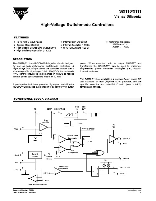
High-Voltage Switchmode ControllersFEATURESD 10- to 120-V Input Range D Current-Mode ControlD High-Speed, Source-Sink Output Drive DHigh Efficiency Operation (> 80%)D Internal Start-Up Circuit D Internal Oscillator (1 MHz)D SHUTDOWN and RESETD Reference SelectionSi9110 − "1%Si9111 − "10%DESCRIPTIONThe Si9110/9111 are BiC/DMOS integrated circuits designed for use as high-performance switchmode controllers. A high-voltage DMOS input allows the controller to work over a wide range of input voltages (10- to 120-VDC). Current-mode PWM control circuitry is implemented in CMOS to reduce internal power consumption to less than 10 mW.A push-pull output driver provides high-speed switching for MOSPOWER devices large enough to supply 50 W of outputpower. When combined with an output MOSFET and transformer, the Si9110/9111 can be used to implement single-ended power converter topologies (i.e., flyback,forward, and cuk).The Si9110/9111 are available in a standard 14-pin plastic DIP and standard or lead (Pb)-free SOIC package, and are specified over the and industrial, D suffix (−40 to 85_C)temperature ranges.FUNCTIONAL BLOCK DIAGRAMFB COMP DISCHARGEBIASV REFV CC+V INOSC OUTOSC INPre-Regulator/Start-UpABSOLUTE MAXIMUM RATINGSVoltages Referenced to −V IN (Note: V CC < +V IN + 0.3 V)V CC 15 V . . . . . . . . . . . . . . . . . . . . . . . . . . . . . . . . . . . . . . . . . . . . . . . . . . . . . . . . . +V IN 120 V . . . . . . . . . . . . . . . . . . . . . . . . . . . . . . . . . . . . . . . . . . . . . . . . . . . . . . . Logic Inputs (RESET,SHUTDOWN, OSC IN, OSC OUT)−0.3 V to V CC + 0.3 V . . . . . . . . . . . . . . . Linear Inputs(FEEDBACK, SENSE, BIAS, V REF )−0.3 V to V CC + 0.3 V . . . . . . . . . . . . . . . HV Pre-Regulator Input Current (continuous) 5 mA . . . . . . . . . . . . . . . . . . . . . Storage Temperature −65 to 150_C . . . . . . . . . . . . . . . . . . . . . . . . . . . . . . . . . . Operating Temperature −40 to 85_C. . . . . . . . . . . . . . . . . . . . . . . . . . . . . . . . . Junction Temperature (T J )150_C . . . . . . . . . . . . . . . . . . . . . . . . . . . . . . . . . . . . Power Dissipation (Package)a14-Pin Plastic DIP (J Suffix)b 750 mW . . . . . . . . . . . . . . . . . . . . . . . . . . . . . . . . 14-Pin SOIC (Y Suffix)c 900 mW . . . . . . . . . . . . . . . . . . . . . . . . . . . . . . . . . . . . Thermal Impedance (Q JA )14-Pin Plastic DIP 167_C/W . . . . . . . . . . . . . . . . . . . . . . . . . . . . . . . . . . . . . . . . . 14-Pin SOIC 140_C/W . . . . . . . . . . . . . . . . . . . . . . . . . . . . . . . . . . . . . . . . . . . . . Notesa.Device mounted with all leads soldered or welded to PC board.b.Derate 6 mW/_C above 25_C.c.Derate 7.2 mW/_C above 25_C.RECOMMENDED OPERATING RANGEVoltages Referenced to −V INV CC 9.5 V to 13.5 V . . . . . . . . . . . . . . . . . . . . . . . . . . . . . . . . . . . . . . . . . . . . . . . . +V IN 10 V to 120 V . . . . . . . . . . . . . . . . . . . . . . . . . . . . . . . . . . . . . . . . . . . . . . . . f OSC 40 kHz to 1 MHz. . . . . . . . . . . . . . . . . . . . . . . . . . . . . . . . . . . . . . . . . . . . . R OSC 25 k W to 1 M W . . . . . . . . . . . . . . . . . . . . . . . . . . . . . . . . . . . . . . . . . . . . . . Linear Inputs 0 to V CC − 3 V . . . . . . . . . . . . . . . . . . . . . . . . . . . . . . . . . . . . . . . . Digital Inputs 0 to V CC. . . . . . . . . . . . . . . . . . . . . . . . . . . . . . . . . . . . . . . . . . . . . SPECIFICATIONS aTest ConditionsUnless Otherwise SpecifiedDISCHARGE = D Suffix−40 to 85_CParameterSymbol−V IN = 0 V V CC = 10 V, +V IN = 48 V R BIAS = 390 k W , R OSC = 330 k WTemp b Min d Typ c Max dUnitReferenceSi9110Room 3.92 4.0 4.08OSC IN = − V IN (OSC Disabled)Si9111Room 3.60 4.04.40Output VoltageV RSi9110Full 3.86 4.14VR L = 10 M WSi9111Full 3.52 4.46Output Impedance e Z OUT Room 153045k W Short Circuit Current I SREF V REF = −V INRoom 70100130m A Temperature Stability eT REFFull0.50 1.0mV/_C OscillatorMaximum Frequency e f MAX R OSC = 0Room 13MHz R OSC = 330 k, See Note f Room 80100120Initial Accuracy f OSC R OSC = 150 k, See Note f Room 160200240kHz Voltage Stability D f/f D f/f=f(13.5 V) − f(9.5 V)/ f(9.5 V)Room 1015%Temperature Coefficient eT OSCFull200500ppm/_CError AmplifierFB Tied to COMP Si9110Room 3.96 4.00 4.04Feedback Input Voltage V FB OSC IN = − V IN (OSC Disabled)Si9111Room 3.604.00 4.40V Input BIAS Current I FB OSC IN = − V IN , V FB = 4 VRoom 25500nA Input OFFSET Voltage V OS Room "15"40mV Open Loop Voltage Gain e A VOL OSC IN = Room 6080dB Unity Gain Bandwidth e BW − V IN (OSC Disabled)Room 1 1.3MHz Dynamic Output Impedance e Z OUT Room 10002000W Source (V FB = 3.4 V)Room −2.0−1.4Output Current I OUT Sink (V FB = 4.5 V)Room 0.120.15mA Power Supply Rejection PSRR9.5 V v V CC v 13.5 VRoom5070dBSPECIFICATIONS aD Suffix−40 to 85_CTest ConditionsDISCHARGE = ParameterUnitMax dTyp c Min d Temp b Unless Otherwise Specified−V IN = 0 V V CC = 10 V, +V IN = 48 V R BIAS = 390 k W , R OSC = 330 k WSymbolCurrent LimitThreshold Voltage V SOURCEV FB = 0 VRoom 1.01.2 1.4V Delay to Output et dV SENSE = 1.5 V, See Figure 1Room100150nsPre-Regulator/Start-UpInput Voltage+V IN I IN = 10 m A Room 120V Input Leakage Current +I IN V CC w 9.4 VRoom 10m A Pre-Regulator Start-Up Current I START Pulse Width v 300 m s, V CC = V ULVORoom 815mAV CC Pre-Regulator Turn-Off Threshold Voltage V REG I PRE-REGULATOR = 10 m ARoom 7.88.69.4Undervoltage Lockout V UVLO Room 7.08.18.9VV REG −V UVLOV DELTARoom0.30.6SupplySupply Current I CC C LOAD < 75 pF (Pin 4)Room 0.450.6 1.0mA Bias CurrentI BIASRoom101520m ALogicSHUTDOWN Delay e t SD C L = 500 pF, V SENSE −V IN , See Figure 2Room 50100SHUTDOWN Pulse Width e t SW See Figure 3Room 50RESET Pulse Width et RW Room 50nsLatching Pulse WidthSHUTDOWN and RESET Low e t LW See Figure 3Room 25Input Low Voltage V IL Room 2.0Input High VoltageV IH Room 8V Input Current Input Voltage High I IH V IN = 10 V Room 15Input Current Input Voltage LowI ILV IN = 0 V Room−35−25m AOutputOutput High Voltage V OH I OUT = −10 mA Room Full 9.79.5Output Low Voltage V OL I OUT = 10 mARoom Full 0.300.50VOutput Resistance R OUT I OUT = 10 mA, Source or SinkRoom Full 20253050W Rise Time e t r Room 4075Fall Time et fC L = 500 pFRoom4075nsNotesa.Refer to PROCESS OPTION FLOWCHART for additional information.b.Room = 25_C, Full = as determined by the operating temperature suffix.c.Typical values are for DESIGN AID ONLY , not guaranteed nor subject to production testing.d.The algebraic convention whereby the most negative value is a minimum and the most positive a maximum.e.Guaranteed by design, not subject to production test.f.C STRAY Pin 8 = v 5 pF.TIMING WAVEFORMSFIGURE 3.TYPICAL CHARACTERISTICS+V IN vs. +I IN at Start-UpOutput Switching Frequency vs.Oscillator Resistance(V )140120100806040200101520+I IN (mA)+V I N (H z )1 M10 k100 k10 k100 k 1 Mr OSC (W )f O U T FIGURE 4.FIGURE 5.BIAS FB +V IN COMP SENSE RESET OUTPUTSHUTDOWN −V IN V REF V CCDISCHARGE OSC OUTOSC INDual-In-Line and SOIC1234567141312111098Top ViewPIN CONFIGURATIONS AND ORDERING INFORMATIONORDERING INFORMATIONPart NumberTemperature Range PackageSi9110DY Si9110DY -T1Si9110DY -T1—E3Si9111DY SOIC-14Si9111DY -T1CSi9111DY -T1—E3−40 to 85_Si9110DJ Si9110DJ-T1PDIP 14Si9111DJ PDIP-14Si9111DJ-T1DETAILED DESCRIPTIONPre-Regulator/Start-Up SectionDue to the low quiescent current requirement of theSi9110/9111 control circuitry, bias power can be supplied from the unregulated input power source, from an external regulated low-voltage supply, or from an auxiliary “bootstrap”winding on the output inductor or transformer.When power is first applied during start-up, +V IN (pin 2) will draw a constant current. The magnitude of this current is determined by a high-voltage depletion MOSFET device which is connected between +V IN and V CC (pin 6). This start-up circuitry provides initial power to the IC by charging an external bypass capacitance connected to the V CC pin. The constant current is disabled when V CC exceeds 8.6 V. If V CC is not forced to exceed the 8.6-V threshold, then V CC will be regulated to a nominal value of 8.6 V by the pre-regulator circuit.As the supply voltage rises toward the normal operating conditions, an internal undervoltage (UV) lockout circuit keeps the output driver disabled until V CC exceeds the undervoltage lockout threshold (typically 8.1 V). This guarantees that the control logic will be functioning properly and that sufficient gate drive voltage is available before the MOSFET turns on.The design of the IC is such that the undervoltage lockout threshold will be at least 300 mV less than the pre-regulator turn-off voltage. Power dissipation can be minimized by providing an external power source to V CC such that the constant current source is always disabled.Note: During start-up or when V CC drops below 8.6V the start-up circuit is capable of sourcing up to 20 mA. This maylead to a high level of power dissipation in the IC (for a 48-V input, approximately 1 W). Excessive start-up time caused by external loading of the V CC supply can result in device damage. Figure 6 gives the typical pre-regulator current at BiC/DMOS as a function of input voltage.BIASTo properly set the bias for the Si9110/9111, a 390-k W resistor should be tied from BIAS (pin 1) to −V IN (pin 5). This determines the magnitude of bias current in all of the analog sections and the pull-up current for the SHUDOWN and RESET pins. The current flowing in the bias resistor is nominally 15m A.Reference SectionThe reference section of the Si9110 consists of a temperature compensated buried zener and trimmable divider network.The output of the reference section is connected internally to the non-inverting input of the error amplifier. Nominal reference output voltage is 4 V. The trimming procedure that is used on the Si9110 brings the output of the error amplifier (which is configured for unity gain during trimming) to within "1% of 4 V.This compensates for input offset voltage in the error amplifier.The output impedance of the reference section has been purposely made high so that a low impedance external voltage source can be used to override the internal voltage source, if desired, without otherwise altering the performance of the device.DETAILED DESCRIPTION (CONT’D)Applications which use a separate external reference, such as non-isolated converter topologies and circuits employing optical coupling in the feedback loop, do not require a trimmed voltage reference with 1% accuracy. The Si9111accommodates the requirements of these applications at a lower cost, by leaving the reference voltage untrimmed. The 10% accurate reference thus provided is sufficient to establish a dc bias point for the error amplifier.Error AmplifierClosed-loop regulation is provided by the error amplifier, which is intended for use with “around-the-amplifier” compensation.A MOS differential input stage provides for low input current.The noninverting input to the error amplifier (V REF ) is internally connected to the output of the reference supply and should be bypassed with a small capacitor to ground.Oscillator SectionThe oscillator consists of a ring of CMOS inverters, capacitors,and a capacitor discharge switch. Frequency is set by an external resistor between the OSC IN and OSC OUT pins.(See Figure 5 for details of resistor value vs. frequency.) The DISCHARGE pin should be tied to −V IN for normal internal oscillator operation. A frequency divider in the logic section limits switch duty cycle to v 50% by locking the switching frequency to one half of the oscillator frequency.Remote synchronization is accomplished by capacitive coupling of a positive SYNC pulse into the OSC IN (pin 8)terminal. For a 5-V pulse amplitude and 0.5-m s pulse width,typical values would be 100 pF in series with 3 k W to pin 8.SHUTDOWN and RESETSHUTDOWN (pin 11) and RESET (pin 12) are intended for overriding the output MOSFET switch via external controllogic. The two inputs are fed through a latch preceding the output switch. Depending on the logic state of RESET,SHUTDOWN can be either a latched or unlatched input. The output is off whenever SHUTDOWN is low. By simultaneously having SHUTDOWN and RESET low, the latch is set and SHUTDOWN has no effect until RESET goes high. The truth table for these inputs is given in Table 1.Table 1: Truth Table for the SHUTDOWN and RESET PinsBoth pins have internal current source pull-ups and should be left disconnected when not in use. An added feature of the current sources is the ability to connect a capacitor and an open-collector driver to the SHUTDOWN or RESET pins to provide variable shutdown time.Output DriverThe push-pull driver output has a typical on-resistance of 20 W .Maximum switching times are specified at 75 ns for a 500-pF load. This is sufficient to directly drive MOSFETs such as the 2N7004, 2N7005, IRFD120 and IRFD220. Larger devices can be driven, but switching times will be longer, resulting in higher switching losses. In order to drive large MOSPOWER devices,it is necessary to use an external driver IC, such as the Vishay Siliconix D469A. The D469A can switch very large devices such as the SMM20N50 (500 V, 0.3 W ) in approximately 100 ns.APPLICATIONSGND−48 V+5 V@ 0.75 A−5 V@ 0.25 ACC FIGURE 6.5-Watt Power Supply for T elecom Applications。
MAXIM MAX9110 MAX9112 说明书
General DescriptionThe MAX9110/MAX9112 single/dual low-voltage differ-ential signaling (LVDS) transmitters are designed for high-speed applications requiring minimum power con-sumption, space, and noise. Both devices support switching rates exceeding 500Mbps while operating from a single +3.3V supply, and feature ultra-low 250ps (max) pulse skew required for high-resolution imaging applications, such as laser printers and digital copiers.The MAX9110 is a single LVDS transmitter, and the MAX9112 is a dual LVDS transmitter.Both devices conform to the EIA/TIA-644 LVDS standard.They accept LVTTL/CMOS inputs and translate them to low-voltage (350mV) differential outputs, minimizing elec-tromagnetic interference (EMI) and power dissipation.These devices use a current-steering output stage, mini-mizing power consumption, even at high data rates. The MAX9110/MAX9112 are available in space-saving 8-pin SOT23 and SO packages. Refer to the MAX9111/MAX9113 data sheet for single/dual LVDS line receivers.________________________ApplicationsFeatures♦Low 250ps (max) Pulse Skew for High-Resolution Imaging and High-Speed Interconnect♦Space-Saving 8-Pin SOT23 and SO Packages ♦Pin-Compatible Upgrades to DS90LV017/017A and DS90LV027/027A (SO Packages)♦Guaranteed 500Mbps Data Rate ♦Low 22mW Power Dissipation at 3.3V (31mW for MAX9112)♦Conform to EIA/TIA-644 Standard ♦Single +3.3V Supply♦Flow-Through Pinout Simplifies PC Board Layout ♦Driver Outputs High Impedance when Powered OffMAX9110/MAX9112Single/Dual LVDS Line Drivers withUltra-Low Pulse Skew in SOT23________________________________________________________________Maxim Integrated Products 1Pin Configurations/Functional Diagrams/Truth Table19-1771; Rev 0; 9/00For free samples and the latest literature, visit or phone 1-800-998-8800.For small orders, phone 1-800-835-8769.Ordering InformationLaser Printers Digital Copiers Cellular Phone Base StationsTelecom Switching EquipmentNetwork Switches/Routers LCD DisplaysBackplane Interconnect Clock DistributionTypical Operating Circuit appears at end of data sheet.M A X 9110/M A X 9112Single/Dual LVDS Line Drivers with Ultra-Low Pulse Skew in SOT23ABSOLUTE MAXIMUM RATINGSELECTRICAL CHARACTERISTICSAC CHARACTERISTICSStresses beyond those listed under “Absolute Maximum Ratings” may cause permanent damage to the device. These are stress ratings only, and functional operation of the device at these or any other conditions beyond those indicated in the operational sections of the specifications is not implied. Exposure to absolute maximum rating conditions for extended periods may affect device reliability.Supply Voltage (V CC to GND)..................................-0.3V to +4V Input Voltage (V DIN_ to GND).....................-0.3V to (V CC + 0.3V)Output Voltage (V DO _+, V DO _- to GND or V CC )...-0.3V to +3.9V Output Short-Circuit Duration(DO_+, DO_- to V CC or GND)................................Continuous ESD Protection (Human Body Model, DO_+, DO_-)..........±11kVContinuous Power Dissipation (T A = +70°C)8-Pin SOT23 (derate 7.52mW/°C above +70°C)...........602mW 8-Pin SO (derate 5.88mW/°C above +70°C)...............471mW Operating Temperature Range ...........................-40°C to +85°C Storage Temperature Range.............................-65°C to +150°C Lead Temperature (soldering,10s)..................................+300°CMAX9110/MAX9112Single/Dual LVDS Line Drivers withUltra-Low Pulse Skew in SOT23_______________________________________________________________________________________3AC CHARACTERISTICS (continued)(V CC = +3.0V to +3.6V, R L = 100Ω±1%, C L = 5pF, T A = -40°C to +85°C, unless otherwise noted. Typical values are at V CC = +3.3V,T A = +25°C.) (Notes 3, 4, 5; Figures 2, 3)Note 2:By definition, current into the device is positive and current out of the device is negative. Voltages are referred to deviceground except V OD .Note 3:AC parameters are guaranteed by design and characterization.Note 4:C L includes probe and fixture capacitance.Note 5:Signal generator conditions for dynamic tests: V OL = 0, V OH = 3V, f = 20MHz, 50% duty cycle, R O = 50Ω, t R ≤1ns, and t F ≤1ns (0 to 100%).Note 6:t SKD1is the magnitude difference of differential propagation delays in a channel; t SKD1 = |t PHLD - t PLHD |.Note 7:t SKD2is the magnitude difference of the t PLHD or t PHLD of one channel and the t PLHD or t PHLD of the other channel on thesame device (MAX9112).Note 8:t SKD3is the magnitude difference of any differential propagation delays between devices at the same V CC and within 5°Cof each other.Note 9:t SKD4is the magnitude difference of any differential propagation delays between devices operating over the rated supplyand temperature ranges.Note 10:f MAX signal generator conditions: V OL = 0, V OH = +3V, frequency = 250MHz, t R ≤1ns, t F ≤1ns (0 to 100%) 50% duty cycle.Transmitter output criteria: duty cycle = 45% to 55%, V OD ≥250mV.Typical Operating Characteristics(V CC = +3.3V, R L = 100Ω, C L = 5pF, V IH = +3V, V IL = GND, f IN = 20MHz, T A = +25°C, unless otherwise noted.) (Figures 2, 3)11001MMAX9110SUPPLY CURRENT vs. INPUT FREQUENCYINPUT FREQUENCY (Hz)S U P P L Y C U R R E N T (m A )9.56.57.07.58.08.59.010k100M1G6.46.76.66.56.86.97.07.17.27.37.4-4010-15356085SUPPLY CURRENT vs. TEMPERATUREM A X 9110 t o c 02TEMPERATURE (°C)C U R R E N T S U P P L Y (m A )0.81.21.01.61.41.82.03.0 3.2 3.33.1 3.4 3.5 3.6DIFFERENTIAL PROPAGATION DELAYvs. SUPPLY VOLTAGESUPPLY VOLTAGE (V)P R O P A G A T I O N D E L A Y (n s )M A X 9110/M A X 9112Single/Dual LVDS Line Drivers with Ultra-Low Pulse Skew in SOT234_______________________________________________________________________________________Typical Operating Characteristics (continued)(V CC = +3.3V, R L = 100Ω, C L = 5pF, V IH = +3V, V IL = GND, f IN = 20MHz, T A = +25°C, unless otherwise noted.) (Figures 2, 3)2502753003253503754004254503.03.23.13.33.43.53.6M A X 9110 t o c 10SUPPLY VOLTAGE (V)D I F F E R E N T I A L O U T P U T V O L T A G E (m V )DIFFERENTIAL OUTPUT VOLTAGEvs. SUPPLY VOLTAGE25027530032535037540042545075.0100.087.5112.5125.0137.5150.0LOAD RESISTANCE (Ω)D I F FE R E N T I A L O U T P U T V O L T A G E (m V )DIFFERENTIAL OUTPUT VOLTAGEvs. LOAD RESISTANCE0.81.21.01.61.41.82.0-4010-15356085TEMPERATURE (°C)P R O P A G A T I O N D E L A Y (n s )DIFFERENTIAL PROPAGATION DELAYvs. TEMPERATURE206040801003.03.23.13.33.43.53.6M A X 9110 t o c 05SUPPLY VOLTAGE (V)D I F FE R E N T I A L P U L S E S K E W (p s )DIFFERENTIAL PULSE SKEW vs. SUPPLY VOLTAGE020604080100-4010-15356085DIFFERENTIAL PULSE SKEWvs. TEMPERATURETEMPERATURE (°C)D I F FE R E N T I A L P U L S E S K E W (p s )3003504004505005506006507003.03.23.13.33.43.53.6TRANSITION TIME vs. SUPPLY VOLTAGESUPPLY VOLTAGE (V)T R A N S I T I O N T I M E (p s )400460440420480500520540560580600-4010-15356085TRANSITION TIME vs. TEMPERATURETEMPERATURE (°C)T R A N S I T I O N T I M E (p s )1.001.151.101.051.201.251.301.351.401.451.503.0 3.23.1 3.3 3.4 3.5 3.6OUTPUT VOLTAGE vs. SUPPLY VOLTAGESUPPLY VOLTAGE (V)O U T P U T V O L T A G E (V )MAX9110/MAX9112Single/Dual LVDS Line Drivers withUltra-Low Pulse Skew in SOT23_______________________________________________________________________________________51.351.381.371.361.391.401.411.421.431.441.4575.0100.087.5112.5125.0137.5150.0LOAD RESISTANCE (Ω)O U T P U T H I G H V O L T A G E (V )OUTPUT HIGH VOLTAGE vs. LOAD RESISTANCE1.001.031.021.011.041.051.061.071.081.091.1075.0100.087.5112.5125.0137.5150.0LOAD RESISTANCE (Ω)O U T P U T L O W V O L T A G E (V )OUTPUT LOW VOLTAGE vs. LOAD RESISTANCETypical Operating Characteristics (continued)(V CC = +3.3V, R L = 100Ω, C L = 5pF, V IH = +3V, V IL = GND, f IN = 20MHz, T A = +25°C, unless otherwise noted.) (Figures 2, 3)Pin DescriptionDetailed DescriptionThe MAX9110/MAX9112 single/dual LVDS transmitters are intended for high-speed, point-to-point, low-power applications. These devices accept CMOS/LVTTL inputs with data rates exceeding 500Mbps. The MAX9110/MAX9112 reduce power consumption andEMI by translating these signals to a differential voltage in the 250mV to 450mV range across a 100Ωload while drawing only 9.4mA of supply current for the dual-channel MAX9112.A current-steering approach induces less ground bounce and no shoot-through current, enhancing noise margin and system speed performance. The outputM A X 9110/M A X 9112Single/Dual LVDS Line Drivers with Ultra-Low Pulse Skew in SOT236_______________________________________________________________________________________Figure 1. LVDS Transmitter V OD and V OS Test CircuitFigure 2. Transmitter Propagation Delay and Transition Time Test Circuitstage presents a symmetrical, high-impedance output,reducing differential reflection and timing distortion. The driver outputs are short circuit current limited and enter a high-impedance state when the device is not powered.LVDS OperationThe LVDS interface standard is a signaling method intended for point-to-point communication over a con-trolled impedance medium as defined by the EIA/TIA-644 LVDS standard. The LVDS standard uses a lower voltage swing than other common communication stan-dards, achieving higher data rates with reduced power consumption while reducing EMI emissions and system susceptibility to noise.LVDS transmitters such as the MAX9110/MAX9112convert CMOS/LVTTL signals to low-voltage differential signals at rates in excess of 500Mbps. The MAX9110/MAX9112 current-steering architecture requires a resis-tive load to terminate the signal and complete the trans-mission loop. Because the device switches the direc-tion of current flow and not voltage levels, the actual output voltage swing is determined by the value of the termination resistor at the input of an LVDS receiver.Logic states are determined by the direction of current flow through the termination resistor. With a typical 3.5mA output current, the MAX9110/MAX9112 produce an output voltage of 350mV when driving a 100Ωload.The steady-state-voltage peak-to-peak swing is twice the differential voltage, or 700mV (typ).Applications InformationSupply BypassingBypass V CC with high-frequency surface-mount ceramic 0.1µF and 0.001µF capacitors in parallel, as close to the device as possible, with the smaller valued capacitor the closest. For additional supply bypassing, place a 10µF tantalum or ceramic capacitor at the point where power enters the circuit board.Figure 3. Transmitter Propagation Delay and Transition Time WaveformsDifferential TracesOutput trace characteristics affect the performance of the MAX9110/MAX9112. Use controlled impedance traces to match trace impedance to both transmission medium impedance and termination resistor. Eliminate reflections and ensure that noise couples as common mode by running the differential traces close together.Reduce skew by matching the electrical length of the traces. Excessive skew can result in a degradation of magnetic field cancellation.Maintain the distance between the differential traces to avoid discontinuities in impedance. Avoid 90°turns and minimize the number of vias to further prevent imped-ance discontinuities.Cables and ConnectorsTransmission media should have a differential charac-teristic impedance of about 100Ω. Use cables and con-nectors that have matched impedance to minimize impedance discontinuities.Avoid the use of unbalanced cables, such as ribbon or simple coaxial cable. Balanced cables, such as twisted pair, offer superior signal quality and tend to generate less EMI due to canceling effects. Balanced cables tend to pick up noise as common mode, which is rejected by the LVDS receiver.TerminationTermination resistors should match the differential char-acteristic impedance of the transmission line. Because the MAX9110/MAX9112 are current-steering devices,an output voltage will not be generated without a termi-nation resistor. Output voltage levels are dependent upon the termination resistor value. Resistance values may range between 75Ωand 150Ω.Minimize the distance between the termination resistor and receiver inputs. Use a single 1% to 2% surface-mount resistor across the receiver inputs.Board LayoutFor LVDS applications, a four-layer PC board that pro-vides separate power, ground, LVDS signals, and input signals is recommended. Isolate the input and LVDS sig-nals from each other to prevent coupling. Separate the input and LVDS signal planes with the power and ground planes for best results.MAX9110/MAX9112Single/Dual LVDS Line Drivers withUltra-Low Pulse Skew in SOT23_______________________________________________________________________________________7MAX9110 TRANSISTOR COUNT: 765MAX9112 TRANSISTOR COUNT: 765PROCESS: CMOSChip InformationTypical Operating CircuitM A X 9110/M A X 9112Single/Dual LVDS Line Drivers with Ultra-Low Pulse Skew in SOT23Maxim cannot assume responsibility for useof any circuitry othe r than circuitry e ntire ly e mbodie d in a Maxim product. No circuit pate nt lice nse s are implied. Maxim reserves the right to change the circuitry and specifications without notice at any time.8_____________________Maxim Integrated Products, 120 San Gabriel Drive, Sunnyvale, CA 94086 408-737-7600©2000 Maxim Integrated ProductsPrinted USAis a registered trademark of Maxim Integrated Products.Package Information。
什么是电子电路中的数字电位器它们有什么作用

什么是电子电路中的数字电位器它们有什么作用在电子电路中,数字电位器是一种用于调节电路中电压或电流的元件。
它们被广泛应用于各种电子设备中,如通信设备、计算机和消费类电子产品。
数字电位器通过改变电阻值来调节电路的参数,从而实现电路的功能控制和调整。
数字电位器通常由一个调节旋钮和一组电子开关组成。
调节旋钮用于手动控制电位器的数值,而电子开关用于根据输入信号或电路需求自动调节电位器的数值。
这些开关可以实现数字信号的转换和控制,使得电路可以根据需要实现不同的功能。
数字电位器可以分为单通道和多通道两种类型。
单通道数字电位器只有一个可调节的输出通道,而多通道数字电位器则可以同时调节多个输出通道。
多通道数字电位器的应用范围更广,可以同时调节多个电路参数,提高电路的灵活性和功能性。
数字电位器在电子电路中有许多重要的作用。
以下是其中几个常见的应用:1. 电压调节:数字电位器可以用于调节电路中的电压,使得电路可以适应不同的电源电压或需求。
通过改变电位器的数值,可以调整电压引脚之间的电压差,从而实现对电路功能的控制。
2. 电流控制:数字电位器可以用于控制电路中的电流大小。
通过改变电位器的数值,可以调节电流引脚之间的电阻,从而改变电路中的电流流动。
这在一些需要对电流进行精确控制的应用中非常重要。
3. 信号选择:数字电位器可以用于选择不同的输入信号或输出信号。
通过改变电位器的数值,可以选择不同的输入通道或输出通道,从而实现对信号的选择和切换。
4. 数字转换:数字电位器可以用于将模拟信号转换为数字信号或数字信号转换为模拟信号。
通过改变电位器的数值,可以将输入信号转换为数字形式进行处理或将数字信号转换为模拟形式进行输出。
5. 参数调节:数字电位器可以用于调节电路中的各种参数,如频率、幅度、相位等。
通过改变电位器的数值,可以实现对电路参数的精确控制,从而满足不同的应用需求。
总之,数字电位器在电子电路中具有重要的作用。
它们通过调节电路的电压、电流和信号选择等功能,实现了电子设备的灵活性和可控性。
LG9110电机驱动芯片介绍
LG9110电机驱动芯片介绍
陌尘
【期刊名称】《《电子制作》》
【年(卷),期】2004(000)011
【摘要】LG9110是为控制和驱动电机设计的两通道推挽式功率放大专用集成电
路器件.将分立电路集成在单片IC之中.使外围器件成本降低.整机可靠性提高。
该芯片有两个TTL/CMOS兼容电平的输入,具有良好的抗干扰性:两个输出端能直接驱动电机的正反向运动.它具有较大的电流驱动能力.每通道能通过750—800mA的持续电流,
【总页数】1页(P45)
【作者】陌尘
【作者单位】
【正文语种】中文
【中图分类】TN929.53
【相关文献】
1.电机控制集成电路的选用——第二十讲内置译码器的步进电机微步进驱动芯片
A3977 [J], 杨旭强;吴红星
2.大联大推出第三代智能车用电机驱动芯片的电机控制器解决方案 [J], ;
3.TFT LCD液晶监视器驱动芯片Source driver介绍(上) [J], 谢崇凯
4.将直流电机驱动芯片应用于开环式高精度步进电机细分控制 [J], 刘佳
5.基于A3988电机驱动芯片的电机控制电路设计 [J], 王烁;田书林;戴志坚
因版权原因,仅展示原文概要,查看原文内容请购买。
数字电位器知识
数字电位器的应用(整理转摘)1用数字电位器替代机械式电位器数字电位器的写次数很容易达到50000次,而机械式电位器的调节次数一般只有几千次,甚至几百次。
目前市场上提供的数字电位器的分辨率在32级(5位)到256级(8位)甚至更高。
对于像LCD显示器对比度调节或其它动态范围要求不高的应用,设计时可以选用低分辨率、低成本的数字电位器。
而高分辨率的数字电位器则被广泛用于动态范围高达90dB的音频和Hi-Fi设备中。
数字电位器具有易失和非易失两种类型,非易失数字电位器与机械式电位器很相似,它们无论上电与否都可以保持电阻值设置,特别是MAX5427/MAX5428/MAX5429数字电位器,更具有独特的编程特性,每个器件带有一个一次性编程(OTP)存储器,能够在上电复位(POR)时将抽头位置设置在用户定义的数值,且抽头位置保持可调,但在上电时总是返回到所设置的位置。
另外,利用OTP功能也可以关闭接口操作,使抽头位置始终保持在所希望的地方。
这样,器件就像一个阻值固定的分压器,而不是电位器。
大多数数字电位器可以通过传统的I2C或SPI接口进行编程,有些器件则采用上/下脉冲计数调节方式。
采用数字电位器有很多优势,首先,这些电位器对灰尘、污垢和潮湿的环境不敏感,而这些因素对于机械式电位器来说则是致命的。
数字电位器几乎能够在任何电子系统中替代老式的机械电位器,而不仅仅是在音频产品,图1列出了数字电位器的几种典型应用。
2数字电位器在音频设备中的应用与机械式电位器相比,数字电位器的另一优势是可以直接安装在电路板的信号通道上,而不需要复杂、昂贵的机械与电控的整合方案。
数字电位器可提高电子噪声抑制能力,不存在机械电位器连线拾取的干扰信号。
传统的数字电位器只是简单地直接取代机械式电位器,它们具有相同的使用方法,因而无需做过多的说明。
然而,对于特殊用途的器件,(如低成本立体声音量控制),使用时可能会出现一些特殊问题。
数字电位器可以提供对数和线性变化函数,对数变化的数字电位器常用于Hi-Fi音频设备中的音量调节,可为具有非线性响应特性的人耳建立一个线性变化的音量控制。
数字电位器是啥

数字电位器是啥数字电位器是啥数字电位器(DigitalPotenTIometer)亦称数控可编程电阻器,是一种替代传统机械电位器(仿照电位器)的新式CMOS数字、仿照混合信号处理的集成电路。
数字电位器由数字输入操控,发作一个仿照量的输出。
根据数字电位器的纷歧样,抽头电流最大值能够从几百微安到几个毫安。
数字电位器选用数控办法调度电阻值的,具有运用活络、调度精度高、无触点、低噪声、不易污损、抗振荡、抗烦扰、体积小、寿数长等显着利益,可在很多范畴替代机械电位器。
数字电位器WDH22也称为非触摸式电位器,是一种用数字传感器查看转轴的视点改动,并将这个视点改动用多种信号类型反响输出的器材。
数字电位器WDH22与机械式电位器FCP22E比照,具有可程控改动有用电气视点及输出计划、耐哆嗦、噪声小、寿数长等利益,因而,已在主动查看与操控、智能仪器外表、船只设备、风力发电等很多首办法域得到成功运用。
数字电位器撤消了电阻基片和电刷,是一个半导体集成电路。
其利益为:调度精度高;没有噪声,有极长的作业寿数;无机械磨损;用于主动操控系统能够完毕对视点方位的精确丈量,也能够运用输出反响信号与视点改动成线性份额的特性,经过驱动转轴完毕输出调度功用。
数字电位器通常由视点传感器电路、数据处理电路、信号改换电路构成。
视点传感器电路是数字电位器的首要构成有些,它将视点改动量搜集改换成随视点改动的仿照信号。
数据处理电路是一种分外的模/数改换电路,改换后的数字量代表0~360deg;的视点值。
信号改换电路根据需求将视点值改换成仿照量(电压/电流)信号或串行数字信号输出。
数字电位器通常带有总线接口,可经过单片机或逻辑电路进行编程。
它适宜构成各种可编程仿照器材,如可编程增益拓宽器、可编程滤波器、可编程线性稳压电源及腔调/音量操控电路,真实完毕了把仿照器材放到总线上(即单片机经过总线操控系统的仿照功用块)这一全新计划理念。
因为数字电位器可替代机械式电位器,所以二者在原理上有相似的本地。
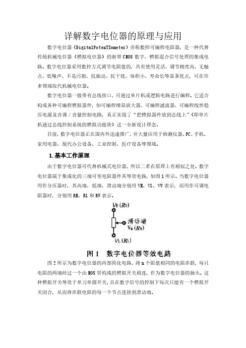
X9250四路数字控制电位器中文资料
原理框图四路数字控制电位器 (XDCP™)特点•四个电位器在一个封装 •256电阻 taps/pot - 0.4%分辨率 •SPI 串行接口•抽头电阻,40Ω典型@ VCC=5V •四个非易失性数据寄存器每个锅 •非易失性存储的抽头位置 •待机电流<5μA 最大(总包) •电源-VCC= 2.7V 至5.5V -V += 2.7V 至5.5V-V-=-2.7V 至-5.5V•100k Ω的,总50K Ω电阻锅 •高可靠性 - 耐力 - 100,000每个数据位每变动 寄存器- 寄存器的数据保留 - 百年 24引脚SOIC ,24引脚TSSOP 封装 X9251的双电源版本 说明该X9250集成了4个数字控制电位器(XDCP )在单片CMOS 集成电路。
该数字控制电位器是通过使用一系列的阵列255的电阻元件来实现。
每个元素之间都通过交换机连接到电位器滑臂终端抽头点。
电位器滑臂的阵列上的位置是由用户通过SPI 总线接口控制。
每个电位器有一个与之相关的挥发性电位器滑臂计数器寄存器(WCR )和4个非易失性数据寄存器(DR0:DR3),可直接写入和由用户读取。
该WCR 的内容控制滑动端的电阻阵列虽然交换机上的位置。
电召回DR0的内容到WCR 。
该XDCP 可以作为一个三端电位或在各种各样的应用,包括控制,参数调整和信号处理两端子可变电阻。
引脚说明串行输出(SO)SO是串行数据输出引脚。
在读周期,数据移出该引脚。
数据的时钟由串行时钟的下降沿。
串行输入SI是串行数据输入引脚。
所有操作码,字节地址和要写入的盆和锅寄存器的数据输入该引脚上。
数据由串行时钟的上升沿锁存。
串行时钟(SCK)该SCK输入用于时钟数据流入和流出X9250的。
片选(CS)当CS为高电平时,X9250是取消和SO引脚处于高阻抗,(除非内部写周期正在进行)的设备将处于待机状态。
CS低使X9250,将其放置在有源电力模式。
应该指出,经过上电,一高向低跳变CS是之前的任何行动开始所需。
一文读懂之电位器知识全知道

一文读懂之电位器知识全知道电位器是一种通用的机电元件, 在仪器仪表和各种电子设备中已获得广泛应用。
电位器是电阻值可以调节变化的电阻,是一种可调的电子元件。
它是由一个电阻体和一个转动或滑动系统组成。
当电阻体的两个固定触点之间外加一个电压时,通过转动或滑动系统改变触点在电阻体上的位置,在动触点与固定触点之间便可得到一个与动触点位置成一定关系的电压。
在家用电器和其他电子设备电路中,电位器的作用是用来分压、分流和用来作为变阻器。
常用于阻值经常调整且要求阻值稳定可靠的场合,在电路中主要通过改变阻值来调节电压和电流的大小,常用于各类需调整工作点、频率点的电子产品中。
电位器的结构电位器通常有三个引出端子,其中有两个固定端,固定端之间的阻值最大,为电位器的标称值;另一端子为活动端子,通过改变活动端子与固定端子间的位置,可以改变相应端子间的电阻值。
其典型电位器基本结构如下图所示,均由电阻体、滑动臂、转轴、外壳和焊片构成。
它有三个引出端,其中 AC 两端电阻值最大, AB 、 BC 之间的电阻值可以通过与转轴相连的簧片位置不同而加以改变。
电位器的分类从构造形式来看, 电位器可分为线绕电位器和非线绕电位器两大类:1、线绕电位器是将电阻丝绕在金属、陶瓷和塑料骨架上作为电阻元件, 具有电阻温度系数低, 电阻值稳定性好, 功率负荷性大,工作寿命长等优点。
但线绕电阻元件的主要缺陷是分辩力有一定阶梯性, 同时多圈的电阻元件的感抗会呈现随频率增加而增加, 因此高频性能差。
此外, 还存在总阻值范围窄等缺点。
2、非线绕电位器有合成膜电位器、玻璃釉电位器、导电塑料电位器等。
1)合成膜电位器是将炭黑、石墨和有机粘合剂、填充料等混合制成的浆料采用多种方法(如丝网印刷) 涂覆在基体上再经固化而制成的电阻膜作为电阻体。
合成碳膜电位器能大规模生产, 价格便宜, 调节时噪声较小, 优越的高频性能, 还具有较小的电感量和分布容量, 且工作寿命长, 很少突然发生严重损坏, 总阻值范围宽广。
详解数字电位器的原理与应用.
详解数字电位器的原理与应用数字电位器(DigitalPotenTIometer)亦称数控可编程电阻器,是一种代替传统机械电位器(模拟电位器)的新型CMOS数字、模拟混合信号处理的集成电路。
数字电位器采用数控方式调节电阻值的,具有使用灵活、调节精度高、无触点、低噪声、不易污损、抗振动、抗干扰、体积小、寿命长等显著优点,可在许多领域取代机械电位器。
数字电位器一般带有总线接口,可通过单片机或逻辑电路进行编程。
它适合构成各种可编程模拟器件,如可编程增益放大器、可编程滤波器、可编程线性稳压电源及音调/音量控制电路,真正实现了“把模拟器件放到总线上”(即单片机通过总线控制系统的模拟功能块)这一全新设计理念。
目前,数字电位器正在国内外迅速推广,并大量应用于检测仪器、PC、手机、家用电器、现代办公设备、工业控制、医疗设备等领域。
1.基本工作原理由于数字电位器可代替机械式电位器,所以二者在原理上有相似之处。
数字电位器属于集成化的三端可变电阻器件其等效电路,如图l所示。
当数字电位器用作分压器时,其高端、低端、滑动端分别用VH、VL、VW表示;而用作可调电阻器时,分别用RH、RL和RW表示。
图2所示为数字电位器的内部简化电路,将n个阻值相同的电阻串联,每只电阻的两端经过一个由MOS管构成的模拟开关相连,作为数字电位器的抽头。
这种模拟开关等效于单刀单掷开关,且在数字信号的控制下每次只能有一个模拟开关闭合,从而将串联电阻的每一个节点连接到滑动端。
数字电位器的数字控制部分包括加减计数器、译码电路、保存与恢复控制电路和不挥发存储器等4个数字电路模块。
利用串入、并出的加/减计数器在输入脉冲和控制信号的控制下可实现加/减计数,计数器把累计的数据直接提供给译码电路控制开关阵列,同时也将数据传送给内部存储器保存。
当外部计数脉冲信号停止或片选信号无效后,译码电路的输出端只有一个有效,于是只选择一个MOS管导通。
数字控制部分的存储器是一种掉电不挥发存储器,当电路掉电后再次上电时,数字电位器中仍保存着原有的控制数据,其中间抽头到两端点之间的电阻值仍是上一次的调整结果。
X9C102系列数字电位器

DESCRIPTIONThe Xicor X9C102/103/104/503 is a solid state nonvola-tile potentiometer and is ideal for digitally controlledresistance trimming.The X9C102/103/104/503 is a resistor array composed of 99 resistive elements. Between each element and at either end are tap points accessible to the wiper element.The position of the wiper element is controlled by the CS ,U/D , and INC inputs. The position of the wiper can be stored in nonvolatile memory and then be recalled upon a subsequent power-up operation.The resolution of the X9C102/103/104/503 is equal to the maximum resistance value divided by 99. As an example, for the X9C503 (50K Ω) each tap point repre-sents 505Ω.All Xicor nonvolatile memories are designed and tested for applications requiring extended endurance and data retention.FEATURES•Compatible with X9102/103/104/503•Low Power CMOS —V CC = 5V—Active Current, 3mA Max —Standby Current, 500µA Max •99 Resistive Elements—Temperature Compensated—± 20% End to End Resistance Range •100 Wiper Tap Points—Wiper Positioned via Three-Wire Interface —Similar to TTL Up/Down Counter —Wiper Position Stored in Nonvolatile Memory and Recalled on Power-Up•100 Year Wiper Position Data Retention •X9C102 = 1K Ω•X9C103 = 10K Ω•X9C503 = 50K Ω•X9C104 = 100K ΩE 2POT ™ Nonvolatile Digital PotentiometerX9C102/103/104/503E 2POT ™ is a trademark of Xicor, Inc.3863 FHD F01FUNCTIONAL DIAGRAML WHVX9C102/103/104/503PIN DESCRIPTIONSV H and V LThe high (V H) and low (V L) terminals of the X9C102/103/ 104/503 are equivalent to the fixed terminals of a mechanical potentiometer. The minimum voltage is –5V and the maximum is +5V. It should be noted that the terminology of V L and V H references the relative position of the terminal in relation to wiper movement direction selected by the U/D input and not the voltage potential on the terminal.V WV W is the wiper terminal, equivalent to the movable terminal of a mechanical potentiometer. The position of the wiper within the array is determined by the control inputs. The wiper terminal series resistance is typically 40Ω.Up/Down (U/D)The U/D input controls the direction of the wiper movement and whether the counter is incremented or decremented.Increment (INC)The INC input is negative-edge triggered. Toggling INC will move the wiper and either increment or decrement the counter in the direction indicated by the logic level on the U/D input.Chip Select (CS)The device is selected when the CS input is LOW. The current counter value is stored in nonvolatile memory when CS is returned HIGH while the INC input is also HIGH. After the store operation is complete the X9C102/ 103/104/503 will be placed in the low power standby mode until the device is selected once again.PIN CONFIGURATIONPIN NAMESSymbol DescriptionV H High TerminalV W Wiper TerminalV L Low TerminalV SS GroundV CC Supply VoltageU/D Up/Down InputINC Increment InputCS Chip Select InputNC No Connect3863 PGM T01V CCCSV LV W3863 FHD F02.2INCU/DV HV SS12348765X9C102/103/104/503DIP/SOICX9C102/103/104/503DEVICE OPERATIONThere are three sections of the X9C102/103/104/503: the input control, counter and decode section; the non-volatile memory; and the resistor array. The input control section operates just like an up/down counter. The output of this counter is decoded to turn on a single electronic switch connecting a point on the resistor array to the wiper output. Under the proper conditions the contents of the counter can be stored in nonvolatile memory and retained for future use. The resistor array is comprised of 99 individual resistors connected in series. At either end of the array and between each resistor is an electronic switch that transfers the potential at that point to the wiper.The INC, U/D and CS inputs control the movement of the wiper along the resistor array. With CS set LOW the X9C102/103/104/503 is selected and enabled to respond to the U/D and INC inputs. HIGH to LOW transitions on INC will increment or decrement (depending on the state of the U/D input) a seven-bit counter. The output of this counter is decoded to select one of one-hundred wiper positions along the resistive array.The wiper, when at either fixed terminal, acts like its mechanical equivalent and does not move beyond the last position. That is, the counter does not wrap around when clocked to either extreme.The value of the counter is stored in nonvolatile memory whenever CS transistions HIGH while the INC input is also HIGH.When the X9C102/103/104/503 is powered-down, the last counter position stored will be maintained in the nonvolatile memory. When power is restored, the con-tents of the memory are recalled and the counter is reset to the value last stored.OPERATION NOTESThe system may select the X9C102/103/104/503, move the wiper, and deselect the device without having to store the latest wiper, position in nonvolatile memory. The wiper movement is performed as described above; once the new position is reached, the system would the keep INC LOW while taking CS HIGH. The new wiper position would be maintained until changed by the system or until a power-down/up cycle recalled the previously stored data.This would allow the system to always power-up to a preset value stored in nonvolatile memory; then during system operation minor adjustments could be made. The adjustments might be based on user preference: system parameter changes due to temperature drift, etc...The state of U/D may be changed while CS remains LOW. This allows the host system to enable the X9C102/103/104/503 and then move the wiper up and down until the proper trim is attained.T IW/R TOTALThe electronic switches on the X9C102/103/104/503 operate in a “make before break” mode when the wiper changes tap positions. If the wiper is moved several positions, multiple taps are connected to the wiper for t IW (INC to V W change). The R TOTAL value for the device can temporarily be reduced by a significant amount if the wiper is moved several positions.R TOTAL with V CC RemovedThe end to end resistance of the array will fluctuate once V CC is removed.SYMBOL TABLEX9C102/103/104/503ABSOLUTE MAXIMUM RATINGS*Temperature under Bias..................–65°C to +135°C Storage Temperature.......................–65°C to +150°C Voltage on CS, INC, U/D and V CCwith Respect to V SS...............................–1V to +7V Voltage on V H and V LReferenced to V SS.................................–8V to +8V ∆V = |V H–V L|X9C102 (4V)X9C103, X9C503, and X9C104 (10V)Lead Temperature (Soldering, 10 seconds)....+300°C Wiper Current.....................................................±1mA *COMMENTStresses above those listed under “Absolute Maximum Ratings” may cause permanent damage to the device. This is a stress rating only and the functional operation of the device at these or any other conditions above those listed in the operational sections of this specifica-tion is not implied. Exposure to absolute maximum rating conditions for extended periods may affect device reliability.ANALOG CHARACTERISTICSElectrical CharacteristicsEnd-to-End Resistance Tolerance (20)Power Rating at 25°CX9C102.......................................................16mW X9C103, X9C503, and X9C104..................10mW Wiper Current............................................±1mA Max. Typical Wiper Resistance.........................40Ω at 1mA Typical Noise..........................< –120dB/Hz Ref: 1VResolution Resistance.............................................................1%LinearityAbsolute Linearity(1)........................................±1.0 Ml(2) Relative Linearity(3).....................................±0.2 Ml(2)Temperature Coefficient(–40°C to +85°C)X9C102......................................+600 ppm/°C Typical X9C103, X9C503, X9C104........+300 ppm/°C Typical Ratiometric Temperature Coefficient............±20 ppm Wiper AdjustabilityUnlimited Wiper Adjustment (Non-Store operation) Wiper Position Store Operations...................10,000 Data Changes Physical CharacteristicsMarking IncludesManufacturer‘s TrademarkResistance Value or CodeDate CodeTest Circuit #1Test Circuit #2Notes:(1)Absolute Linearity is utilized to determine actual wiper voltage versus expected voltage= (V w(n)(actual) – V w(n)(expected)) = ±1 Ml Maximum.(2) 1 Ml = Minimum Increment = R TOT/99.(3)Relative Linearity is a measure of the error in step size between taps = V W(n+1) – [V w(n) + Ml] = +0.2 Ml.X9C102/103/104/503 RECOMMENDED OPERATING CONDITIONSTemperature Min.Max. Commercial0°C+70°C Industrial–40°C+85°C Military–55°C+125°C3863 PGM T03.1Supply Voltage Limits X9C102/103/104/5035V ±10%D.C. OPERATING CHARACTERISTICS (Over recommended operating conditions unless otherwise specified.)LimitsSymbol Parameter Min.Typ.(4)Max.Units Test ConditionsI CC V CC Active Current13mA CS = V IL, U/D = V IL or V IH andINC = 0.4V to 2.4V @ max. t CYCI SB Standby Supply Current200500µA CS = V CC – 0.3V, U/D and INC =V SS or V CC – 0.3VI LI CS, INC, U/D Input±10µA V IN = V SS to V CCLeakage CurrentV IH CS, INC, U/D Input2V CC + 1VHIGH VoltageV IL CS, INC, U/D Input–10.8VLOW VoltageR W Wiper Resistence40100ΩMax. Wiper Current ±1mAV H VH Terminal Voltage–5+5VV L VL Terminal Voltage–5+5VC IN(5)CS, INC, U/D Input10pF V CC = 5V, V IN = V SS,Capacitance T A = 25°C, f = 1MHz3863 PGM T05.3 STANDARD PARTSPart Number Maximum Resistance Wiper Increments Minimum Resistance X9C1021KΩ10.1Ω40ΩX9C10310KΩ101Ω40ΩX9C50350KΩ505Ω40ΩX9C104100KΩ1010Ω40Ω3863 PGM T08.1 Notes:(4)Typical values are for T A = 25°C and nominal supply voltage.(5)This parameter is periodically sampled and not 100% tested.3863 PGM T04.2X9C102/103/104/503MODE SELECTIONA.C. CONDITIONS OF TESTNotes:(6)Typical values are for T A = 25°C and nominal supply voltage.(7)This parameter is periodically sampled and not 100% tested.(8)MI in the A.C. timing diagram refers to the minimum incremental change in the V W output due to a change in the wiper position.X9C102/103/104/503Typical Frequency Response for X9C102TEST CONDITIONS V CC = 5VTemp. = 25°C Wiper @ Tap 50V H = 0.5V RMSNormalized (0dB @ 1KHz)Test Circuit #1TEST CONDITIONS V CC = 5VTemp. = 25°C Wiper @ Tap 50V H = 2V RMS Test Circuit #1Typical Total Harmonic Distortion for X9C102N O R M A L I Z E D G A I N (d B )9630–3–6–9–12–15–18–210.010.101.0010.00100.001000.0010000.00FREQUENCY IN KHzT H D (%)2.01.81.61.41.21.00.80.60.40.20.00.010.101.0010.00100.001000.0010000.00FREQUENCY IN KHz3863 FHD F063863 FHD F07X9C102/103/104/503Typical Linearity for X9C102Typical Frequency Response for X9C103TEST CONDITIONS V CC = 5VTemp. = 25°C Wiper @ Tap 50V H = 0.5V RMSNormalized (0dB @ 1KHz)Test Circuit #1N O R M A L I Z E D G A I N (d B )9630–3–6–9–12–15–18–210.010.101.0010.00100.001000.00FREQUENCY IN KHz3863 FHD F09X9C102/103/104/503Typical Total Harmonic Distortion for X9C103Typical Linearity for X9C103TEST CONDITIONS V CC = 5VTemp. = 25°C Wiper @ Tap 50V H = 2V RMS Test Circuit #1T H D (%)2.01.81.61.41.21.00.80.60.40.20.00.010.101.0010.00100.001000.00FREQUENCY IN KHz3863 FHD F10X9C102/103/104/503Typical Frequency Response for X9C503Typical Total Harmonic Distortion for X9C503TEST CONDITIONS V CC = 5VTemp. = 25°C Wiper @ Tap 50V H = 2V RMS Test Circuit #1TEST CONDITIONS V CC = 5VTemp. = 25°C Wiper @ Tap 50V H = 0.5V RMSNormalized (0dB @ 1 KHz)Test Circuit #19630-3-6-9-12-15-18-210.010.101.0010.00100.00FREQUENCY IN KHzN O R M A L I Z E D G A I N (d B )1000.0091.81.61.41.21.00.80.60.40.20.00.010.101.0010.00100.00FREQUENCY IN KHzT H D (%)1000.003863 FHD F123863 FHD F13X9C102/103/104/503Typical Linearity for X9C503Typical Frequency Response for X9C104TEST CONDITIONS V CC = 5VTemp. = 25°C Wiper @ Tap 50V H = 0.5V RMSNormalized (0dB @ 1 KHz)Test Circuit #19630-3-6-9-12-15-18-210.010.101.0010.00100.001000.00FREQUENCY IN KHzN O R M A L I Z E D G A I N (d B )3863 FHD F15X9C102/103/104/503Typical Total Harmonic Distortion for X9C104Typical Linearity for X9C104TEST CONDITIONS V CC = 5VTemp. = 25°C Wiper @ Tap 50V H = 2V RMS Test Circuit #12.01.81.61.41.21.00.80.60.40.20.00.010.101.0010.00100.0010000.00FREQUENCY IN KHzT H D (%)1000.003863 FHD F16X9C102/103/104/5033926 FHD F01TYP NOTE: ALL DIMENSIONS IN INCHES (IN PARENTHESES IN MILLIMETERS)MAX.PACKAGING INFORMATION8-LEAD PLASTIC DUAL IN-LINE PACKAGE TYPE PNOTE: ALL DIMENSIONS IN INCHES (IN PARENTHESES IN MILLIMETERS)X9C102/103/104/503PACKAGING INFORMATION8-LEAD PLASTIC SMALL OUTLINE GULL WING PACKAGE TYPE SNOTE: ALL DIMENSIONS IN INCHES (IN PARENTHESIS IN MILLIMETERS)3926 FHD F22X9C102/103/104/503ORDERING INFORMATIONX9CXXX X XTemperature RangeBlank = Commercial = 0°C to +70°CI = Industrial = –40°C to +85°CM = Military = –55°C to +125°CPackageP = 8-Lead Plastic DIPS = 8-Lead SOICEnd to End Resistance102 = 1KΩ103 = 10KΩ503 = 50KΩ104 = 100KΩLIMITED WARRANTYDevices sold by Xicor, Inc. are covered by the warranty and patent indemnification provisions appearing in its Terms of Sale only. Xicor, Inc. makes no warranty, express, statutory, implied, or by description regarding the information set forth herein or regarding the freedom of the described devices from patent infringement. Xicor, Inc. makes no warranty of merchantability or fitness for any purpose. Xicor, Inc. reserves the right to discontinue production and change specifications and prices at any time and without notice.Xicor, Inc. assumes no responsibility for the use of any circuitry other than circuitry embodied in a Xicor, Inc. product. No other circuits, patents, licenses are implied.U.S. PATENTSXicor products are covered by one or more of the following U.S. Patents: 4,263,664; 4,274,012; 4,300,212; 4,314,265; 4,326,134; 4,393,481; 4,404,475;4,450,402; 4,486,769; 4,488,060; 4,520,461; 4,533,846; 4,599,706; 4,617,652; 4,668,932; 4,752,912; 4,829, 482; 4,874, 967; 4,883, 976. Foreign patents and additional patents pending.LIFE RELATED POLICYIn situations where semiconductor component failure may endanger life, system designers using this product should design the system with appropriate error detection and correction, redundancy and back-up features to prevent such an occurence.Xicor's products are not authorized for use in critical components in life support devices or systems.1.Life support devices or systems are devices or systems which, (a) are intended for surgical implant into the body, or (b) support or sustain life, and whosefailure to perform, when properly used in accordance with instructions for use provided in the labeling, can be reasonably expected to result in a significant injury to the user.2.A critical component is any component of a life support device or system whose failure to perform can be reasonably expected to cause the failure of the lifesupport device or system, or to affect its safety or effectiveness.。
3.4 数字电位器

X9AX5400 1
MAX5401
X9110
1
数字接口 按键 脉冲线 脉冲线
I2C 接口 SPI
SPI
总阻值
抽头数 易失性
10kΩ
32
非
(2.1/5/10/50) kΩ 64
是
(10/50) kΩ
100
非
(2/10/50) kΩ
64
非
(50/100) kΩ
256 非
电源电压 ±5V
端位置是跨步变化的,由模拟开关闭合位置决定。模拟开关闭合位置受数字接口控制,因此称数字电位器。数字电位
器内的电阻是由半导体制成,阻值精度低(误差为 15%~20%), 但各电阻阻值一致性好,相对误差<1%。
数字电位器在应用中有 2 种接法:可调分压器、可调电阻器。在可调分压器应用中,滑动端的负载电阻通常很大,滑 动端分压取决于抽头位置比值,与数字电位器总阻值无关,数字电位器总阻值无关。在可调电阻器中,数字电位器作 为可调电阻,其阻值为总阻值乘以抽头位置比,阻值精度与数字电位器阻值精度相当。
滑动端位置建立时间:>0.3uS。 5. 滑动端输出电流:输出电流通常只有±1mA。有的数字电位器具有输出缓冲器,输出电流可达到±20mA 6. 滑动端电阻:即模拟开关电阻,数值在几十Ω到一百几十Ω。
五. 数字电位器典型产品(直线型)
类型 步 进 式 数 置 式
型号
通道数
X9511
1
MCP4011 1
2. 数置式,步进式 数置式数字电位器的抽头位置控制是通过写入位置代码 实现的,数字接口形式为 SPI、I2C 等。 步进式数字电位器的抽头位置是脉冲控制的,管脚 1 个脉冲使抽头步进 1 个位置。数字接口形式 为按键式、脉冲线式等。
SIHFL9110中文资料

Power MOSFETIRFL9110, SiHFL9110Vishay SiliconixFEATURES•Surface Mount•Available in Tape and Reel •Dynamic dV/dt Rating•Repetitive Avalanche Rated •P-Channel •Fast Switching •Ease of Paralleling•Lead (Pb)-free AvailableDESCRIPTIONThird generation Power MOSFETs from Vishay provide thedesigner with the best combination of fast switching,ruggedized device design, low on-resistance and cost-effectiveness.The SOT-223 package is designed for surface-mount using vapor phase, infrared, or wave soldering techniques. Its unique package design allows for easy automatic pick-and-place as with other SOT or SOIC packages but has the added advantage of improved thermal performance due to an enlarged tab for heatsinking. Power dissipation of greater than 1.25 W is possible in a typical surface mount application.Notea.See device orientation.Notesa.Repetitive rating; pulse width limited by maximum junction temperature (see fig. 11).b.V DD = - 25 V, starting T J = 25 °C, L = 7.7 mH, R G = 25 Ω, I AS = - 4.4 A (see fig. 12).c.I SD ≤ - 4.4 A, dI/dt ≤ - 75 A/µs, V DD ≤ V DS , T J ≤ 150 °C.d. 1.6 mm from case.e.When mounted on 1" square PCB (FR-4 or G-10 material).PRODUCT SUMMARYV DS (V)- 100R DS(on) (Ω)V GS = - 10 V1.2Q g (Max.) (nC)8.7Q gs (nC) 2.2Q gd (nC) 4.1ConfigurationSingleORDERING INFORMATIONPackage SOT-223SOT-223Lead (Pb)-free IRFL9110PbF IRFL9110TRPbF a Si HFL9110-E3 Si H FL210T-E3a SnPbIRFL9110IRFL9110TR a SiHFL9110SiHFL9110T aABSOLUTE MAXIMUM RATINGS T C = 25 °C, unless otherwise notedPA AMETE SYMBOL LIMIT UNIT Drain-Source Voltage V DS - 100VGate-Source Voltage V GS ±20 Continuous Drain Current V GS at - 10 V T C = 25 °C I D- 1.1A T C = 100 °C - 0.69Pulsed Drain Current aI DM - 8.8Linear Derating Factor 0.025W/°C Linear Derating Factor (PCB Mount)e 0.017Single Pulse Avalanche Energy bE AS 100mJ Avalanche Current aI AR - 1.1A Peak Diode Recovery dV/dtc E AR 0.31mJ Maximum Power Dissipation T C = 25 °CP D 3.1W Maximum Power Dissipation (PCB Mount)e T A = 25 °C 2.0Peak Diode Recovery dV/dt cdV/dt - 5.5V/ns Operating Junction and Storage Temperature Range T J , T stg- 55 to + 150 °CSoldering Recommendations (Peak Temperature)for 10 s 300dIRFL9110, SiHFL9110Vishay SiliconixNotea.When mounted on 1" square PCB (FR-4 or G-10 material).Notesa.Repetitive rating; pulse width limited by maximum junction temperature (see fig. 11).b.Pulse width ≤ 300 µs; duty cycle ≤ 2 %.THERMAL RESISTANCE RATINGSPA AMETE SYMBOL MIN.TYP.MAX.UNIT Maximum Junction-to-Ambient (PCB Mount)aR thJA --60°C/WMaximum Junction-to-Case (Drain)R thJC--40IRFL9110, SiHFL9110Vishay Siliconix TYPICAL CHARACTERISTICS 25 °C, unless otherwise notedFig. 1 - Typical Output Characteristics Fig. 2 - Typical Output Characteristics Fig. 3 - Typical Transfer CharacteristicsFig. 4 - Normalized On-Resistance vs. TemperatureIRFL9110, SiHFL9110 Vishay SiliconixFig. 5 - Typical Capacitance vs. Drain-to-Source Voltage Fig. 6 - Typical Gate Charge vs. Gate-to-Source Voltage Fig. 7 - Typical Source-Drain Diode Forward VoltageFig. 8 - Maximum Safe Operating AreaIRFL9110, SiHFL9110Vishay SiliconixFig. 9 - Maximum Drain Current vs. Case TemperatureFig. 10a - Switching Time Test CircuitFig. 10b - Switching Time WaveformsFig. 11 - Maximum Effective Transient Thermal Impedance, Junction-to-CaseIRFL9110, SiHFL9110Vishay SiliconixFig. 12b - Unclamped Inductive WaveformsFig. 12c - Maximum Avalanche Energy vs. Drain CurrentFig. 13a - Basic Gate Charge WaveformFig. 13b - Gate Charge Test CircuitIRFL9110, SiHFL9110Vishay SiliconixVishay Siliconix maintains wor ldwide manufactur ing capability. Pr oducts may be manufactur ed at one of sever al qualified locations. Reliability data for Silicon Technology and Package Reliability represent a composite of all qualified locations. For related documents such as package/tape drawings, par t mar king, and reliability data, see /ppg?91196.Disclaimer Legal Disclaimer NoticeVishayAll product specifications and data are subject to change without notice.Vishay Intertechnology, Inc., its affiliates, agents, and employees, and all persons acting on its or their behalf (collectively, “Vishay”), disclaim any and all liability for any errors, inaccuracies or incompleteness contained herein or in any other disclosure relating to any product.Vishay disclaims any and all liability arising out of the use or application of any product described herein or of any information provided herein to the maximum extent permitted by law. The product specifications do not expand or otherwise modify Vishay’s terms and conditions of purchase, including but not limited to the warranty expressed therein, which apply to these products.No license, express or implied, by estoppel or otherwise, to any intellectual property rights is granted by this document or by any conduct of Vishay.The products shown herein are not designed for use in medical, life-saving, or life-sustaining applications unless otherwise expressly indicated. Customers using or selling Vishay products not expressly indicated for use in such applications do so entirely at their own risk and agree to fully indemnify Vishay for any damages arising or resulting from such use or sale. Please contact authorized Vishay personnel to obtain written terms and conditions regarding products designed for such applications.Product names and markings noted herein may be trademarks of their respective owners.元器件交易网。
EL9110中文资料(Intersil)中文数据手册「EasyDatasheet - 矽搜」
x9111 数字电位器(低功耗1024抽头)
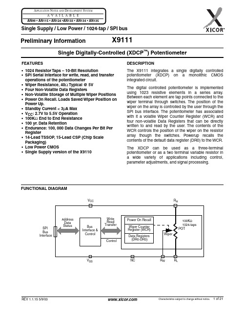
wireless systems • Set the operating points in temperature control
systems • Control the operating point for sensors in industrial
circuits • Provide a control variable (I, V, or R) in feedback
circuits
SYSTEM LEVEL APPLICATIONS
• Adjust the contrast in LCD displays • Control the power level of LED transmitters in
APPLICATION NOTES AND DEVELOPMENT SYSTEM AVAILABLE
AN99 • AN115 • AN124 •AN133 • AN134 • AN135
Single Supply / Low Power / 1024-tap / SPI bus
Preliminary Information
SERIAL CLOCK (SCK)
The SCK input is used to clock data into and out of the X9111.
HOLD (HOLD)
HOLD is used in conjunction with the CS pin to select the device. Once the part is selected and a serial sequence is underway, HOLD may be used to pause the serial communication with the controller without resetting the serial sequence. To pause, HOLD must be brought LOW while SCK is LOW. To resume communication, HOLD is brought HIGH, again while SCK is LOW. If the pause feature is not used, HOLD should be held HIGH at all times.
电位器培训资料

电位器1、概论:用于分压的可变电阻器。
在裸露的电阻体上,紧压着一至两个可移金属触点。
触点位臵确定电阻体任一端与触点间的阻值。
按输出与输入电压比与旋转角度的关系分直线式电位器(呈线性关系)、函数电位器(呈曲线关系)。
主要参数为阻值、容差、额定功率。
2、用途:广泛用于电子设备,在音响和接收机中作音量控制用。
3、结构:电位器是一种可调的电子元件。
它是由一个电阻体和一个转动或滑动系统组成。
当电阻体的两个固定触电之间外加一个电压时,通过转动或滑动系统改变触点在电阻体上的位臵,在动触点与固定触点之间便可得到一个与动触点位臵成一定关系的电压。
它大多是用作分压器,这是电位器是一个四端元件。
电位器基本上就是滑动变阻器,有几种样式,一般用在音像音量开关和激光头/玩具/功率大小调节电位器是一种可调的电子元件。
它是由一个电阻体和一个转动或滑动系统组成。
当电阻体的两个固定触电之间外加一个电压时,通过转动或滑动系统改变触点在电阻体上的位臵,在动触点与固定触点之间便可得到一个与动触点位臵成一定关系的电压。
4、功能:电位器的作用——调节电压(含直流电压与信号电压)和电流的大小。
5、电位器的结构特点——电位器的电阻体有两个固定端,通过手动调节转轴或滑柄,改变动触点在电阻体上的位臵,则改变了动触点与任一个固定端之间的电阻值,从而改变了电压与电流的大小。
6、性能:6.1 电位器的电气性能:A、全阻值(行业俗称总阻) :通常是指电位器上标注的电阻值,它等于电阻体两个固定端之间的电阻值。
其单位有欧姆(Ω),千欧(KΩ),兆欧(MΩ),业内基本以欧姆为单位;表达方式:例B10K意为阻抗变化特性为B线型10000Ω(K代表千或000)。
规格承认书都有允许误差范围。
实测阻值与标称阻值误差范围根据不同精度要求可允许±20%。
±10%。
甚至±5%的误差(但会影响单价)。
精密电位器(如绕线式即多圈式)的精度可达±0.1%。
PXI9100任意波形发生器(数据采集卡)
PXI9100任意波形发生器硬件使用说明书成都九州阿尔泰科技有限公司产品研发部修订第一章功能概述信息社会的发展,在很大程度上取决于信息与信号处理技术的先进性。
数字信号处理技术的出现改变了信息与信号处理技术的整个面貌,而数据采集作为数字信号处理的必不可少的前期工作在整个数字系统中起到关键性、乃至决定性的作用,其应用已经深入到信号处理的各个领域中。
实时信号处理、数字图像处理等领域对高速度、高精度数据采集卡的需求越来越大。
ISA 总线由于其传输速度的限制而逐渐被淘汰。
我公司推出的PXI9100 任意波形发生器卡综合了国内外众多同类产品的优点,以其使用的便捷、稳定的性能、极高的性价比,获得多家试用客户的一致好评,是一款真正具有可比性的产品,也是您理想的选择。
第一节、产品应用本卡是一种基于PXI 总线的任意波形发生器卡,可直接插在IBM-PC/AT 或与之兼容的计算机内的任一PXI 插槽中,构成实验室、产品质量检测中心等各种领域的数据采集、波形分析和处理系统。
也可构成工业生产过程监控系统。
它的主要应用场合为:*电子产品质量检测*信号采集*过程控制*伺服控制第二节、DA波形输出功能◆转换器类型:DAC9765◆输入量程:±5V 、±10V◆转换精度:12 位(Bit)◆点频率(Frequency):1Hz ~80MHz◆物理通道数:2 路同步◆触发方式:软件内触发、硬件外触发◆触发模式(TriggerMode):单次、连续、单步和紧急触发◆时钟源选择(OutClockSource):内时钟和外时钟软件可选◆触发源(TriggerSource ):AT R 触发◆触发方向:正向触发、负向触发、正负向均触发◆触发源AT R 输入范围:-10V~10V2成都九州阿尔泰科技有限公司028-PXI9100任意波形发生器说明书3◆触发电平(TrigLevelV olt ):软件可调,触发电平软件可调(-10V~10V )◆存储器深度:每路512K字点RAM存储器◆每路可指定任意一段RAM做任意循环输出的数据◆数据传输方式:程序方式◆软件功能校准◆工作温度范围:0 ℃~+70℃◆存储温度范围:-20℃~+70℃第三节、DI数字量输入功能◆通道数:8 路◆电气标准:TTL 兼容◆高电平的最低电压:2V◆低电平的最高电压:0.8V第四节、DO 数字量输出功能◆通道数:8 路◆电气标准:TTL 兼容◆高电平的最低电压:3.8V◆低电平的最高电压:0.44V◆上电输出:低电平第五节、其他指标◆板载时钟振荡器:80MHz第六节、产品安装核对表打开PXI9100 板卡包装后,你将会发现如下物品:1、PXI9100 板卡一个;2、ART 软件光盘一张,该光盘包括如下内容:a)本公司所有产品驱动程序,用户可在PXI 目录下找到PXI9100 驱动程序;b)用户手册(pdf 格式电子文档)。
eaton 9SX 8000 9SX 11000 安装和用户手册说明书

版权所有 © 2012 EATON 保留所有权利。
服务和支持:请致电您当地的服务代表8-11kVA EU_CN9SX 80009SX 110009PX 80009PX 110009SX EBM 240V 9PX EBM 240V安装和用户手册第 2 页8-11kVA EU_CN安全说明保存这些说明。
本手册包含一些重要说明,在安装和维护 UPS 和电池过程中应加以遵循。
本手册中介绍的 9SX 和 9PX 型号适合安装在温度介于 0°C 到 40°C 之间且不存在导电污染物的环境中。
已对本设备进行测试,且结果符合 FCC 规则第 15 部分中规定的关于 A 类数字设备的限制。
这些限制旨在提供合理的保护,以防止设备在商用环境中运行时遭到有害干扰。
此设备会产生、使用且能够辐射射频能量,如果未按照说明手册进行安装和使用,则可能对无线电通信造成有害干扰。
在住宅区域运行此设备可能导致有害干扰,此时用户需要自行支付纠正干扰产生的费用。
认证标准p 安全性:IEC/EN 62040-1/第 1 版:2008.UL 1778 第 4 版p EMC :IEC/EN 62040-2/第 2 版:2006. FCC 第 15 部分 A 类。
p 性能:IEC/EN 62040-3/第 2.0 版:2011.p IEC 61000-4-2 (ESD):3 级。
p IEC 61000-4-3(辐射场):3 级。
p IEC 61000-4-4 (EFT):4 级。
p IEC 61000-4-5(快速瞬态):4 级。
p IEC 61000-4-6(电磁场):3 级。
p IEC 61000-4-8(导电磁场):4 级。
特殊符号下面举例介绍了 UPS 或配件上使用的用于警告用户重要信息的符号:存在电击危险 – 请遵守与电击危险符号关联的警告。
必须始终遵守的重要说明。
请勿将 UPS 或 UPS 电池混在垃圾中丢弃。
数字电位器在仪器仪表上的应用

数字电位器在仪器仪表上的应用数字电位器(Digital Potentiometer)是一种能够调节电阻值的电子元件,通过数字信号控制,可以在仪器仪表等电路中实现对电阻值的精确调节。
下面将介绍数字电位器在仪器仪表上的应用。
1. 自动化调节:数字电位器可以作为自动化系统中的调节元件,用于控制仪器仪表的灵敏度、增益、阈值等参数。
通过改变数字电位器的阻值,可以实现对仪器仪表的自动校准和调节,提高系统的准确性和稳定性。
2. 增益控制:在信号处理和放大电路中,数字电位器可以用于调节信号的增益。
通过改变数字电位器的阻值,可以改变信号经过放大电路后的增益倍数,使得输出信号满足特定的需求。
3. 数据采集:数字电位器可以用于模拟信号的采集电路中,通过调节数字电位器的阻值,可以改变采集电路的输入电阻,从而调节电路的输入灵敏度和范围。
这在实验测量和传感器信号处理中非常有用。
4. 音频调节:在音频设备中,数字电位器可以用于音量控制和音调调节。
通过改变数字电位器的阻值,可以调节音频信号的音量大小和音调高低,实现音频设备的音频输出控制。
5. 数字衰减器:数字电位器还可以用作数字衰减器,用于衰减信号的幅度。
通过改变数字电位器的阻值,可以实现对信号的衰减,常见的应用包括音频系统中的音量控制和可调衰减放大器。
6. 电路校准:数字电位器可以用于仪器仪表的电路校准。
通过改变数字电位器的阻值,可以调整电路中的参数,使其满足标准要求,提高仪器仪表的准确性和可靠性。
7. 数字控制系统:数字电位器可以与微控制器或数字信号处理器等数字控制系统结合使用,实现对电路参数的精确控制。
通过与数字控制系统的通信,可以动态地改变数字电位器的阻值,从而实现对仪器仪表的远程控制和调节。
总之,数字电位器在仪器仪表上有广泛的应用。
它可以实现对电路参数的精确控制和调节,提高仪器仪表的准确性、稳定性和可靠性。
数字电位器的使用可以简化电路设计,提高系统的灵活性和可调性。
- 1、下载文档前请自行甄别文档内容的完整性,平台不提供额外的编辑、内容补充、找答案等附加服务。
- 2、"仅部分预览"的文档,不可在线预览部分如存在完整性等问题,可反馈申请退款(可完整预览的文档不适用该条件!)。
- 3、如文档侵犯您的权益,请联系客服反馈,我们会尽快为您处理(人工客服工作时间:9:00-18:30)。
X9110单数控电位器 (XDCP™)双电源/低功耗/1024抽头/SPI总线一概述1 1 描述X9110将一个单数控电位器(XDCP)集成在一个单片CMOS集成电路中数控电位器由包含1023个电阻单元的电阻阵列构成在每个电阻单元之间有通过开关连接到滑动端的抽头点阵列中滑动端的位置由用户通过SPI总线接口控制电位器还相应地配有一个易失性滑动端计数寄存器WCR和四个非易失性的数据寄存器这些数据寄存器可由用户直接读出或写入滑动端计数寄存器WCR的内容通过开关控制电阻阵列中滑动端的位置上电时可将默认数据寄存器DR0的内容重新调用至滑动端计数寄存器WCR中XDCP可用作三终端的电位器或两终端的可变电阻应用范围广泛包括控制参数调整和信号处理1 2 特点1024个电阻抽头10位分辨率用于电位器写读和传输操作的SPI串行接口滑动端电阻5V时典型值为40四个非易失性的数据寄存器对滑动端的多个位置进行非易失性存储上电时的重新调用功能上电时装载已保存的滑动端位置待机电流<3A最大值系统V CC 2.7V至5.5V模拟V+/V-5V至+5V100K点对点电阻数据保存期为100年每个寄存器的每位可承受100000次数据擦写14引脚TSSOP封装15引脚CSP封装芯片比例封装与厂商联系可获得双电源类型为X9111低功耗CMOS1 3 应用范围1电路层次应用范围改变电压放大器的增益为比较器和检测器提供可编程的直流电压基准控制音频电路的音量修整电压放大器电路中的偏移电压误差设置稳压器的输出电压调整惠斯通电桥电路中的电阻控制滤波器电路中的增益特性频率和品质因数设置传感器信号调节电路中的比例因子和零点更改定时器电路的频率和占空比改变RF电路中引脚二极管衰减器的直流偏压为反馈电路提供一个控制变量(I V或 R)2系统层次应用范围调整液晶显示屏的对比度控制通讯系统中发光二极管发送器的功率电平设置和调节无线系统中RF功率放大器的直流偏压点 控制音频和家庭娱乐系统的增益为RF无线系统中的调谐器提供可变的直流偏压设置温度控制系统中的工作点控制工业系统中传感器的工作点调整人工智能系统中的偏移和增益误差1 4 功能方框图1简图2详细功能方框图1 5 引脚排列及说明1引脚排列如下图2引脚功能配置表TSSOP CSP13引脚说明总线接口引脚串行输出SOSO是串行数据输出引脚在读操作期间数据从该引脚移出数据在串行时钟的下降沿一位一位地移出串行输入SISI是串行数据输入引脚所有写入电位器和电位器寄存器的操作码字节地址和数据都通过该引脚输入数据由串行时钟的上升沿锁存串行时钟SCKSCK输入脚用于为X9110的数据输入和输出提供时钟HOLDHOLD与CS引脚连接可选中器件一旦器件被选中并且连续的时序开始进行HOLD引脚可用来中止与控制器的连续通信而不用复位连续时序为了中止通信在SCK为低电平时必须将HOLD也拉低为了恢复通信当SCK再次为低电平时必须将HOLD拉高如果不使用中止功能则应该一直HOLD保持引脚为高电平器件地址A0地址输入引脚用于设置8位从地址从地址串行数据流A0必须与地址输入A0引脚匹配以启动与X9110的通信片选脚CS当CS为高电平时X9110不被选中串行输入SO引脚为高阻抗并且除非内部写周期正在进行器件将进入待机状态CS为低电平则使能X9110将其置入有效工作状态应注意在上电后在开始任何操作之前要求在CS脚上有从高到低的跳变硬件写保护输入WP当WP引脚为低时可防止对数据寄存器的非易失性写操作电位器引脚R H R LR H和R L引脚等效于机械电位器的连接端R W滑动引脚等效于机械电位器的滑动端偏压电源引脚系统电源电压(V CC)和电源地(V SS)V CC引脚是系统电源电压脚V SS引脚是系统地脚模拟电源电压(V+和V-)这些电源是电位器的模拟电源电压V+ 电源与滑动端开关连接而V- 电源用于加偏压到开关和集成电路的内部P+衬底这两个电源均可设置电位器的电压极限二工作原理2 1 器件描述串行接口X9110支持SPI接口的硬件协议器件可通过SI输入端访问并且数据在SCK上升沿一位一位被移入在整个操作过程中CS必须为低电平HOLD引脚和WP引脚必须为高电平SO和SI引脚可以连接在一起因为它们有三态输出端这有助于减少系统引脚数电阻阵列说明X9110由电阻阵列构成见图1该阵列包含1023个分立的电阻单元这些电阻单元串行连接阵列的每个物理端等效于机械电位器的固定端R H和R L输入端在阵列的两端和每个电阻单元之间有一个CMOS开关连接到滑动输出端(R W) 在独立的阵列中一次只可接通一个开关这些开关由滑动端计数寄存器WCR控制WCR的10位(WCR[9:0])被解码以选择和使能1024个开关中的一个图1 电位器详细方框图滑动端计数寄存器 (WCR)X9110包含一个滑动端计数寄存器见表1用于XDCP电位器WCR等效于一个串入并出的寄存器/计数器其输出端被解码以沿着电阻阵列从1024个开关中选择一个WCR的内容可以用以下三种方法更改1可由主机通过写滑动端计数寄存器指令串行装载来直接对其写入2可通过传送4个相应数据寄存器之一的内容由XFR数据寄存器间接对其写入3在上电时对其加载数据寄存器0DR0的内容滑动端计数寄存器是一个易失性的寄存器也就是说它的内容在X9110掉电时会丢失尽管在上电时该寄存器会自动加载数据寄存器0DR0的值但这不同于掉电时的值推荐使用上电指南以确保将DR0的值正确地载入WCR中数据寄存器DR电位器有四个10位非易失性的数据寄存器这些寄存器可由主机直接读或写数据也可以在四个数据寄存器中的任何一个和滑动端计数寄存器之间传送所有改变数据寄存器中数据的操作都是非易失性操作最多会耗时10ms如果是不要求存储电位器多个设置值的应用数据寄存器则可用作系统参数或用户选择数据的常规存储区DR[9:0]用于存储1024个滑动端位置(0 ~1023)中的一个见表2状态寄存器SR这个1位状态寄存器用于存储系统的状态见表3WIP正在进行的写操作的状态位只读-当WIP=1时表明高电压写周期正在进行-当WIP=0时表明没有进行高电平写周期表1 滑动端计数寄存器WCR10位WCR9-WCR0用于存储当前滑动端的位置V表示易失性表2 数据寄存器DR10位位9-位0用于存储滑动端位置或数据NV表示非易失性表3 状态寄存器SR1位2 2 器件指令辨识字节ID和A跟随在CS上从高到低跳变后的主机发至X9110的第一个字节即称作辩识字节从地址中的4个最高有效位是器件类型辨识符ID[3:0]位是X9110的器件辨识字节ID它固定为0101[B]见表4ID字节中的A0位是内部从地址器件的物理地址由A0输入引脚的状态来定义从地址由用户在外部规定X9110将串行数据流与地址输入状态进行比较为使X9110可顺利继续命令序列地址位的比较一定要成功只有在器件的从地址与由主机发出的器件输入地址相匹配才能执行该指令A0输入端可由CMOS输入信号或通过将其连接到V CC或V SS来激活R/W位用于设置器件的读或写方式表4 辨识字节格式指令字节和寄存器选择在辨识字节之后发送至X9110的字节包含指令和寄存器指针信息这3个最高有效位用于提供指令操作码(I[2:0])RB和RA位指向四个寄存器中的一个格式如表5所示表5 指令字节格式七个指令中有五个指令的长度为4个字节这些指令是-读滑动端计数寄存器读取选中的电位器的当前滑动端的位置-写滑动端计数寄存器变更选中的电位器的当前滑动端的位置-读数据寄存器读取选中的数据寄存器的内容-写数据寄存器对选中的数据寄存器写入一个新值-读状态该命令恢复WIP位的内容WIP位表明内部写周期是否在进行4字节指令的基本序列如图3所示这些4字节指令在WCR和数据寄存器中的一个之间交换数据数据从数据寄存器传送到WCR实质上是对静态RAM的一次写操作静态RAM控制着滑动端的位置滑动端对该操作的响应会在t WRL时间内延迟从WCR当前滑动端的位置到数据寄存器的一次数据传送也是对非易失性存储器的一次写入最少要耗时t WR才能完成这类数据传送可在电位器和其相应的一个寄存器之间发生读状态寄存器指令是唯一有特殊格式的指令见图4有两个指令要求以一个两字节的序列来完成见图2这两个指令可在主机与X9110之间主机和一个数据寄存器之间或直接在主机和滑动端计数寄存器之间传输数据它们是-XFR数据寄存器到滑动端计数寄存器该指令传输指定数据寄存器的内容到相应的滑动端计数寄存器-XFR滑动端计数寄存器到数据寄存器该指令传输指定滑动端计数寄存器的内容到指定的相应数据寄存器详情请见指令格式正在进行的写操作WIP位器件在接收到一次完整的写序列后CS引脚发生从低到高的跳变此时数据寄存器的内容被存储到非易失性的存储器中此内部写操作的过程可由正在进行的写操作位WIP监控可用读状态命令对WIP位读见图4上电掉电要求V+电压必须一直大于或等于R H或R L端的电压而且R H或R L端的电压必须一直大于或等于V-端的电压在上电和掉电期间VCC V+和V-必须在1ms之内达到各自的最终值图2 两字节指令序列图3 四字节指令序列对WCR或数据寄存器的读或写图4 四字节指令序列读状态寄存器表6 指令集指令格式读滑动端计数寄存器WCR写滑动端计数寄存器WCR读数据寄存器DR写数据寄存器DR传输数据寄存器DR的内容到滑动端计数寄存器WCR传输滑动端计数寄存器WCR的内容到数据寄存器DR读状态寄存器SR注1A0表示主机发出的器件地址2WCRx代表滑动端计数寄存器中滑动端的位置数据3X不必考虑三特性3 1 极限参数工作温度 –65°C至+135°C贮存温度 –65°C至+150°C SCK任何地址输入端上的电压相对于V SS–1V至+7VV+端上的电压相对于V410V4-10VV-端上的电压相对于V(V+) – (V-) 12VR H / R L端上的电压V+R L /R H端上的电压V-引线温度焊接10秒 300°C 10秒±6mAIW注强度超出所列的极限参数可能导致器件的永久性损坏这些仅仅是极限参数并不意味着在极限条件下或在任何其它超出推荐工作条件所示参数的情况下器件能有效工作延长在极限参数条件下的工作时间会影响器件的可靠性3 2 推荐工作条件3 3 模拟特性在推荐的工业级工作条件下 2.7V工作除非另有规定注1绝对线性用于确定实际滑动端的电压与期望滑动端电压之间的差而这在电位器中由滑动端的位置确定2相对线性用于确定电位器中两个相邻抽头位置之间电压的实际变化是对步距误差的测量3MI = RTOT / 1023或(R– R L) / 1023单电位器4V CC, V+, V-在1 ms内必须达到其最终值5n = 0, 1, 2, …,1023; m =0, 1, 2, …, 10223 4 直流工作特性在推荐工作条件下除非另有规定3 5 耐久性和数据保存期3 6 电容37 上电时序注6该参数未经100%测试7t PUR和t PUW是从最后的电源(Vcc-)稳定到可发出特定指令所需要的延迟时间这两个参数未经100%测试8R H, R L, R W引脚上的额定静电放电ESD为1.5KV人体模型HBM最大漏电流1.0µA其它此脚上的静电放电为2.0KV38 交流测试条件输入脉冲电平V CC x0.1 V CC x0.9输入上升和下降时间10ns输入和输出定时电平V CC x0.539 等效交流负载电路310 交流时序311 高电平写周期时序符号参数典型值最大值单位t WR高电平写周期时间存储指令 5 10 ms 312 XDCP数控电位器时序符号参数最小值最大值单位t WRPO在第三路最后的电源稳定后滑动端的响应时间 5 10 s t WRL指令发出后所有装载指令滑动端的响应时间 5 10 s313 符号表四时序表输入时序输出时序HOLD时序XDCP时序对所有负载指令而言写保护和器件地址引脚时序五应用资料电位器基本配置三终端电位器可变分压器两终端可变电阻可变电流应用电路非反向放大器稳压器偏移电压调节带滞后功能的比较器衰减器滤波器反向放大器等效L-R电路函数发生器六封装信息14引脚塑料TSSOP封装类型V七订购信息声明本资料仅参考如有不同之处请以相应英文资料为准。