STM32T215线路连接图
STM32最小系统电路
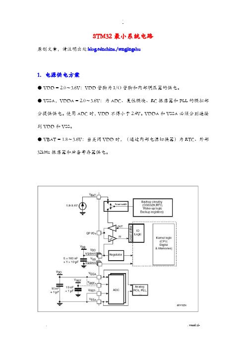
STM32最小系统电路原创文章,请注明出处:blog.ednchina./tengjingshu1.电源供电方案● VDD = 2.0~3.6V:VDD管脚为I/O管脚和内部调压器的供电。
● VSSA,VDDA = 2.0~3.6V:为ADC、复位模块、RC振荡器和PLL的模拟部分提供供电。
使用ADC时,VDD不得小于2.4V。
VDDA和VSSA必须分别连接到VDD和VSS。
● VBAT = 1.8~3.6V:当关闭VDD时,(通过内部电源切换器)为RTC、外部32kHz振荡器和后备寄存器供电。
采用LM1117-3.3V(AMS1117)供电2.晶振STM32上电复位后默认使用内部[精度8MHz左右]晶振,如果外部接了8MHz 的晶振,可以切换使用外部的8MHz晶振,并最终PLL倍频到72MHz。
3.JTAG接口在官方给出的原理图基本是结合STM32三合一套件赠送的ST-Link II给出的JTAG接口。
ST-Link IISK-STM32F学习评估套件原理图的JTAG 连接很多时候为了省钱,所以很多人采用wiggler + H-JTAG的方案。
H-JTAG其实是twentyone大侠开发的调试仿真烧写软件,界面很清新很简洁。
H-JTAG界面H-JTAG软件的下载:.hjtag./chinese/download.htmlH-JTAG官网:.hjtag.twentyone 大侠的blog:twentyone.bokee./关于STM32 H-JTAG的使用,请看下一篇博文Wiggler其实是一个并口下载方案,其实电路图有很多种,不过一些有可能不能使用,所以要注意。
你可以在taobao上买人家现成做好的这种Wiggler下载线,最简便的方法是自己动手做一条,其实很简单,用面包板焊一个74HC244就可以了。
Wiggler电路图下载:电路图中”RESET SELECT”和”RST JUMPER”不接,如果接上的话会识别不了芯片。
STM32原理图含保护电路
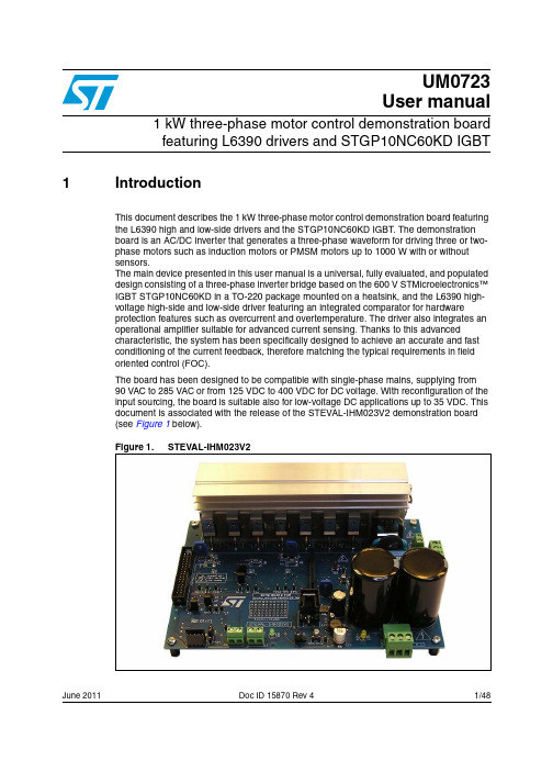
UM0723User manual1 kW three-phase motor control demonstration boardfeaturing L6390 drivers and STGP10NC60KD IGBT 1 IntroductionThis document describes the 1 kW three-phase motor control demonstration board featuringthe L6390 high and low-side drivers and the STGP10NC60KD IGBT. The demonstrationboard is an AC/DC inverter that generates a three-phase waveform for driving three or two-phase motors such as induction motors or PMSM motors up to 1000 W with or withoutsensors.The main device presented in this user manual is a universal, fully evaluated, and populateddesign consisting of a three-phase inverter bridge based on the 600 V STMicroelectronics™IGBT STGP10NC60KD in a TO-220 package mounted on a heatsink, and the L6390 high-voltage high-side and low-side driver featuring an integrated comparator for hardwareprotection features such as overcurrent and overtemperature. The driver also integrates anoperational amplifier suitable for advanced current sensing. Thanks to this advancedcharacteristic, the system has been specifically designed to achieve an accurate and fastconditioning of the current feedback, therefore matching the typical requirements in fieldoriented control (FOC).The board has been designed to be compatible with single-phase mains, supplying from90 VAC to 285 VAC or from 125 VDC to 400 VDC for DC voltage. With reconfiguration of theinput sourcing, the board is suitable also for low-voltage DC applications up to 35 VDC. Thisdocument is associated with the release of the STEVAL-IHM023V2 demonstration board(see Figure1 below).Figure 1.STEVAL-IHM023V2June 2011Doc ID 15870 Rev 41/48Contents UM0723Contents1Introduction . . . . . . . . . . . . . . . . . . . . . . . . . . . . . . . . . . . . . . . . . . . . . . . . 12System introduction . . . . . . . . . . . . . . . . . . . . . . . . . . . . . . . . . . . . . . . . . 62.1Main characteristics . . . . . . . . . . . . . . . . . . . . . . . . . . . . . . . . . . . . . . . . . . 62.2Target applications . . . . . . . . . . . . . . . . . . . . . . . . . . . . . . . . . . . . . . . . . . . 62.3Safety and operating instructions . . . . . . . . . . . . . . . . . . . . . . . . . . . . . . . . 72.3.1General terms . . . . . . . . . . . . . . . . . . . . . . . . . . . . . . . . . . . . . . . . . . . . . 72.3.2Demonstration board intended use . . . . . . . . . . . . . . . . . . . . . . . . . . . . . 72.3.3Demonstration board installation . . . . . . . . . . . . . . . . . . . . . . . . . . . . . . . 72.3.4Electrical connections . . . . . . . . . . . . . . . . . . . . . . . . . . . . . . . . . . . . . . . 82.3.5Demonstration board operation . . . . . . . . . . . . . . . . . . . . . . . . . . . . . . . . 83Board description . . . . . . . . . . . . . . . . . . . . . . . . . . . . . . . . . . . . . . . . . . . 93.1System architecture . . . . . . . . . . . . . . . . . . . . . . . . . . . . . . . . . . . . . . . . . . 93.2The board schematic . . . . . . . . . . . . . . . . . . . . . . . . . . . . . . . . . . . . . . . . 103.3Circuit description . . . . . . . . . . . . . . . . . . . . . . . . . . . . . . . . . . . . . . . . . . . 163.3.1Power supply . . . . . . . . . . . . . . . . . . . . . . . . . . . . . . . . . . . . . . . . . . . . . 163.3.2Inrush limitation . . . . . . . . . . . . . . . . . . . . . . . . . . . . . . . . . . . . . . . . . . . 173.3.3Brake function . . . . . . . . . . . . . . . . . . . . . . . . . . . . . . . . . . . . . . . . . . . . 173.3.4Gate driving circuit . . . . . . . . . . . . . . . . . . . . . . . . . . . . . . . . . . . . . . . . . 183.3.5Overcurrent protection . . . . . . . . . . . . . . . . . . . . . . . . . . . . . . . . . . . . . . 183.3.6Current sensing amplifying network . . . . . . . . . . . . . . . . . . . . . . . . . . . . 193.3.7The tachometer and Hall/encoder inputs . . . . . . . . . . . . . . . . . . . . . . . . 233.3.8Temperature feedback and overtemperature protection . . . . . . . . . . . . 234Hardware setting of the STEVAL-IHM023V2 . . . . . . . . . . . . . . . . . . . . . 244.1Hardware settings for six-step (block commutation) control of BLDCmotors . . . . . . . . . . . . . . . . . . . . . . . . . . . . . . . . . . . . . . . . . . . . . . . . . . . 244.2Hardware settings for “Field Oriented Control” (FOC) in single-shunttopology current reading configuration . . . . . . . . . . . . . . . . . . . . . . . . . . . 264.3Hardware settings for FOC in three-shunt configuration . . . . . . . . . . . . . 27 5Description of jumpers, test pins, and connectors . . . . . . . . . . . . . . . 302/48Doc ID 15870 Rev 4UM0723Contents 6Connector placement . . . . . . . . . . . . . . . . . . . . . . . . . . . . . . . . . . . . . . . 33 7Bill of material . . . . . . . . . . . . . . . . . . . . . . . . . . . . . . . . . . . . . . . . . . . . . 34 8PCB layout . . . . . . . . . . . . . . . . . . . . . . . . . . . . . . . . . . . . . . . . . . . . . . . . 40 9Ordering information . . . . . . . . . . . . . . . . . . . . . . . . . . . . . . . . . . . . . . . 44 10Using STEVAL-IHM023V2 with STM32 PMSM FOC firmwarelibrary v3.0 . . . . . . . . . . . . . . . . . . . . . . . . . . . . . . . . . . . . . . . . . . . . . . . . 4410.1Environmental considerations . . . . . . . . . . . . . . . . . . . . . . . . . . . . . . . . . 4410.2Hardware requirements . . . . . . . . . . . . . . . . . . . . . . . . . . . . . . . . . . . . . . 4510.3Software requirements . . . . . . . . . . . . . . . . . . . . . . . . . . . . . . . . . . . . . . . 4510.4STM32 FOC firmware library v3.0 customization . . . . . . . . . . . . . . . . . . . 45 11Conclusion . . . . . . . . . . . . . . . . . . . . . . . . . . . . . . . . . . . . . . . . . . . . . . . . 47 12References . . . . . . . . . . . . . . . . . . . . . . . . . . . . . . . . . . . . . . . . . . . . . . . . 47 13Revision history . . . . . . . . . . . . . . . . . . . . . . . . . . . . . . . . . . . . . . . . . . . 47Doc ID 15870 Rev 43/48List of tables UM0723 List of tablesTable 1.Current reading configuration. . . . . . . . . . . . . . . . . . . . . . . . . . . . . . . . . . . . . . . . . . . . . . . 23 Table 2.Jumper settings for high-voltage BLDC motor in six-step control. . . . . . . . . . . . . . . . . . . . 24 Table 3.Jumper settings for low-voltage BLDC motor in six-step control . . . . . . . . . . . . . . . . . . . . 25 Table 4.Jumper settings for high-voltage PMAC or generic AC motor in single-shuntFOC control . . . . . . . . . . . . . . . . . . . . . . . . . . . . . . . . . . . . . . . . . . . . . . . . . . . . . . . . . . . . 26 Table 5.Jumper settings for low-voltage BLDC motor in single-shunt FOC control. . . . . . . . . . . . . 27 Table 6.Jumper settings for FOC of HV PMSM, BLDC, or AC IM in three-shunt configuration for current reading . . . . . . . . . . . . . . . . . . . . . . . . . . . . . . . . . . . . . . . . . . . . . . . . . . . . . . . 28 Table 7.Jumper settings for FOC of LV PMSM or BLDC in three-shunt configuration for current reading . . . . . . . . . . . . . . . . . . . . . . . . . . . . . . . . . . . . . . . . . . . . . . . . . . . . . . . . . . 29 Table 8.Jumpers description . . . . . . . . . . . . . . . . . . . . . . . . . . . . . . . . . . . . . . . . . . . . . . . . . . . . . . 30 Table 9.Connector pinout description . . . . . . . . . . . . . . . . . . . . . . . . . . . . . . . . . . . . . . . . . . . . . . . 31 Table 10.Testing pins description . . . . . . . . . . . . . . . . . . . . . . . . . . . . . . . . . . . . . . . . . . . . . . . . . . . 32 Table 11.Bill of material. . . . . . . . . . . . . . . . . . . . . . . . . . . . . . . . . . . . . . . . . . . . . . . . . . . . . . . . . . . 34 Table 12.STEVAL-IHM023V2 motor control workbench parameters . . . . . . . . . . . . . . . . . . . . . . . . 45 Table 13.Document revision history . . . . . . . . . . . . . . . . . . . . . . . . . . . . . . . . . . . . . . . . . . . . . . . . . 47 4/48Doc ID 15870 Rev 4UM0723List of figures List of figuresFigure 1.STEVAL-IHM023V2 . . . . . . . . . . . . . . . . . . . . . . . . . . . . . . . . . . . . . . . . . . . . . . . . . . . . . . . 1 Figure 2.Motor control system architecture. . . . . . . . . . . . . . . . . . . . . . . . . . . . . . . . . . . . . . . . . . . . . 9 Figure 3.STEVAL- IHM023V2 schematic - part 1. . . . . . . . . . . . . . . . . . . . . . . . . . . . . . . . . . . . . . . 10 Figure 4.STEVAL- IHM023V2 schematic - part 2. . . . . . . . . . . . . . . . . . . . . . . . . . . . . . . . . . . . . . . 11 Figure 5.STEVAL- IHM023V2 schematic - part 3. . . . . . . . . . . . . . . . . . . . . . . . . . . . . . . . . . . . . . . 12 Figure 6.STEVAL- IHM023V2 schematic - part 4. . . . . . . . . . . . . . . . . . . . . . . . . . . . . . . . . . . . . . . 13 Figure 7.STEVAL- IHM023V2 schematic - part 5. . . . . . . . . . . . . . . . . . . . . . . . . . . . . . . . . . . . . . . 14 Figure 8.STEVAL- IHM023V2 schematic - part 6. . . . . . . . . . . . . . . . . . . . . . . . . . . . . . . . . . . . . . . 15 Figure 9.Power supply block diagram. . . . . . . . . . . . . . . . . . . . . . . . . . . . . . . . . . . . . . . . . . . . . . . . 17 Figure 10.Gate driving network. . . . . . . . . . . . . . . . . . . . . . . . . . . . . . . . . . . . . . . . . . . . . . . . . . . . . . 18 Figure 11.Overcurrent protection . . . . . . . . . . . . . . . . . . . . . . . . . . . . . . . . . . . . . . . . . . . . . . . . . . . . 19 Figure 12.Three-shunt configuration. . . . . . . . . . . . . . . . . . . . . . . . . . . . . . . . . . . . . . . . . . . . . . . . . . 21 Figure 13.Six-step current sensing configuration . . . . . . . . . . . . . . . . . . . . . . . . . . . . . . . . . . . . . . . . 22 Figure 14.NTC placement on the heatsink. . . . . . . . . . . . . . . . . . . . . . . . . . . . . . . . . . . . . . . . . . . . . 23 Figure 15.STEVAL-IHM023V2 connectors placement . . . . . . . . . . . . . . . . . . . . . . . . . . . . . . . . . . . . 33 Figure 16.Silk screen - top side . . . . . . . . . . . . . . . . . . . . . . . . . . . . . . . . . . . . . . . . . . . . . . . . . . . . . 41 Figure 17.Silk screen - bottom side . . . . . . . . . . . . . . . . . . . . . . . . . . . . . . . . . . . . . . . . . . . . . . . . . . 42 Figure 18.Copper tracks - top side . . . . . . . . . . . . . . . . . . . . . . . . . . . . . . . . . . . . . . . . . . . . . . . . . . . 43 Figure 19.Copper tracks - bottom side . . . . . . . . . . . . . . . . . . . . . . . . . . . . . . . . . . . . . . . . . . . . . . . . 43Doc ID 15870 Rev 45/48System introduction UM07236/48Doc ID 15870 Rev 42 System introduction2.1 Main characteristicsThe information below lists the converter specification data and the main parameters set forthe STEVAL-IHM023V2 demonstration board.●Minimum input voltage 125 VDC or 90 VAC ●Maximum input voltage 400 VDC or 285 VAC●With applied input voltage doubler - the range is from 65 VAC to 145 VAC ●Voltage range for low-voltage motor control applications from 18 VDC to 35 VDC ●Possibility to use auxiliary +15 V supply voltage ●Maximum output power for motors up to 1000 W ●Regenerative brake control feature ●Input inrush limitation with bypassing relay●+ 15 V auxiliary power supply based on buck converter with VIPer™16●IGBT power switch STGP10NC60KD in TO-220 package - compatible with other ST IGBTs or power MOSFETs in TO-220 package●Fully populated board conception with testing points and isolated plastic safety cover ●Motor control connector for interface with STM3210B-EVAL board and other ST motor control dedicated kits ●Tachometer input ●Hall/encoder inputs●Possibility to connect BEMF daughterboard for sensorless six-step control of BLDC motors●PCB type and size:–Material of PCB - FR-4–Double-sided layout –Copper thickness: 60 µm–T otal dimensions of demonstration board: 127 mm x 180 mm.2.2 Target applications●Washing machines ●Home appliances●Medical applications - rehabilitative beds●High-power, high-efficiency water pumps for heating applications.UM0723System introductionDoc ID 15870 Rev 47/482.3 Safety and operating instructions2.3.1 General termsWarning:During assembly, testing, and operation, the demonstrationboard poses several inherent hazards, including bare wires, moving or rotating parts, and hot surfaces. There is a danger of serious personal injury and damage to property, if the kit or components are improperly used or installed incorrectly. The kit is not electrically isolated from the AC/DC input. The demonstration board is directly linked to the mains voltage. No insulation has been placed between the accessible parts and the high-voltage. All measurement equipment must be isolated from the mains before powering the board. When using an oscilloscope with the demonstration board, it must be isolated from the AC line. This prevents a shock from occurring as a result of touching any single point in the circuit, but does NOT prevent shocks when touching two or more points in the circuit. Do not touch the demonstration board after disconnection from the voltage supply, as several parts and power terminals, which contain energized capacitors, need to be allowed to discharge.All operations involving transportation, installation and use, as well as maintenance, are to be carried out by skilled technical personnel (national accident prevention rules must be observed). For the purpose of these basic safety instructions, “skilled technical personnel” are suitably qualified people who are familiar with the installation, use and maintenance of powered electronic systems.2.3.2 Demonstration board intended useThe STEVAL-IHM023V2 demonstration board is a component designed for demonstration purposes only and is not to be used for electrical installation or machinery. The technical data as well as information concerning the power supply conditions should be taken from the documentation and strictly observed.2.3.3 Demonstration board installationThe installation and cooling of the demonstration kit boards must be in accordance with the specifications and the targeted application.●The motor drive converters are protected against excessive strain. In particular, no components are to be bent or isolating distances altered during the course of transportation or handling.●No contact must be made with other electronic components and contacts.●The boards contain electro-statically sensitive components that are prone to damage through improper use. Electrical components must not be mechanically damaged or destroyed.System introduction UM07238/48Doc ID 15870 Rev 42.3.4 Electrical connectionsApplicable national accident prevention rules must be followed when working on the mainpower supply with a motor drive. The electrical installation must be completed in accordance with the appropriate requirements.2.3.5 Demonstration board operationA system architecture which supplies power to the demonstration board should be equipped with additional control and protective devices in accordance with the applicable safety requirements (e.g. compliance with technical equipment and accident prevention rules).UM0723Board descriptionDoc ID 15870 Rev 49/483 Board description3.1 System architectureA generic motor control system can be basically schematized as the arrangement of fourmain blocks (see Figure 2 below).●A control block - its main task is to accept user commands and motor driveconfiguration parameters and to provide all digital signals to implement the proper motor driving strategy. The ST demonstration board based on the STM32™microcontroller STM3210B-EVAL can be used as a control block thanks to the motor control connector used on the board.●A power block - makes a power conversion from the DC bus transferring to the motor by means of a three-phase inverter topology. The power block is based on high-voltage (high and low-side) drivers (L6390) and power switches (STGP10NC60KD) in TO-220 packages.●The motor itself - the STEVAL-IHM023V2 demonstration board is able to properly drive any PMSM, but the FOC itself is conceived for sinusoidal-shaped BEMF . The demonstration board is also suitable for driving any three or two-phase asynchronous motor or low-voltage BLDC motors.●Power supply block - able to work from 90 VAC to 285 VAC or from 125 VDC to400 VDC. With reconfiguration of the power stage with jumpers, the board can also be used for low-voltage applications from 18 VDC to 35 VDC. By supplying the electronic parts on the board through an external + 15 V connector, the board can be used for a wide voltage range up to 400 VDC. Please refer to Section 4 for detailed settings of the jumpers according to the required application.Referring to the above motor control system architecture, the STEVAL-IHM023V2 includes the power supply and the power block hardware blocks.Board description UM0723 3.2 The board schematic10/48Doc ID 15870 Rev 4Doc ID 15870 Rev 411/4812/48Doc ID 15870 Rev 4Doc ID 15870 Rev 413/4814/48Doc ID 15870 Rev 4Doc ID 15870 Rev 415/483.3 Circuitdescriptionsupply3.3.1 PowerThe power supply in the STEVAL-IHM023V2 demonstration board is implemented asa multifunctional block which allows to supply the inverter in all ranges of input voltage up to285 VAC or 400 VDC. If the input AC voltage does not surpass 145 VAC, it is possible toapply the input voltage doubler, this is done by shorting the W14 jumper. This configurationalmost doubles the input AC voltage to a standard level and allows to evaluate the motorcontrol application with a low level of input AC voltage.For high-voltage applications it is necessary to set W3 jumpers to position “HIGHVOLT AGE”, the auxiliary power supply for supplying all active components on thedemonstration board is implemented as a buck converter based on the U6 VIPer16L whichworks with fixed frequency 60 kHz. The output voltage of the converter is +15 VDC voltagewhich is fed into the L6390 drivers as supply voltage as well as into the linear regulatorL78L33ACD and L78M05ACDT. The linear regulator provides +3.3 VDC and +5 VDC forsupplying the operational amplifiers and other related parts placed on the demonstrationboard. The selection of supply voltage for hardware peripherals placed on the board is donewith jumper W1. In the “3.3 V” position the supply voltage selected is +3.3 V and in the “5 V”position it is +5 V. Thanks to jumper W6, it is possible to supply the connected MCU drivingboard with related supply voltage. In this case, the maximal consumptive current of the MCUunit has not overreached 50 mA. Please refer to the ST released VIPer16LD datasheet forfurther information on this concept.For low-voltage applications, the step-down converter must be disabled by setting the W3jumper to position “<35 V ONL Y”. In this case, the other linear regulator, L7815, isconnected directly on the bus line, to provide auxiliary voltage + 15 VDC.Note:Please note that the voltage range in this kind of application must be in the range + 18 VDC to + 35 VDC.For low-voltage DC motor applications which require a voltage lower than + 18 VDC, a dualsupply mode can be used. Voltage on the input connector is normally linked through powerswitches to the motor and an external auxiliary voltage is fed through the J3 connector froman external power source. The voltage of the external power supply used must be in therange + 14.8 V to + 15.5 V with maximal consumption current 0.5 A.The information regarding the value of the supply bus voltage on the main filteringcapacitors is sensed with the voltage divider built around R2, R4, and R7 and is fed into thededicated control unit through the J5 connector. The proper voltage partitioning for appliedresistors values is 0.0075.The presence of +15 VDC on the board is indicated with green LED D7. For a betterunderstanding of the concept, Figure9 describes the power supply in a block diagram.16/48Doc ID 15870 Rev 4limitation3.3.2 InrushThe input stage of the demonstration board is provided with the 10 Ω NTC resistor toeliminate input inrush current peak during charging of the bulk capacitors. T o achievea higher efficiency of the inverter, it is possible to bypass the NTC after the startup phase.The NTC bypass signal is provided from the MCU board through the J5 connector. Theyellow D27 LED diode is turned off when the inrush NTC is bypassed.The STEVAL-IHM023V2 demonstration board contains only a basic EMI filter based on X2and Y2 capacitors. The main function of this demonstration board is as a universal testingplatform. For this reason, the EMI filter is not able to absorb EMI distortion coming from theinverter for all ranges of the applications used and the design of the filter is up to the user.The EMI filter must be designed according to the motor and final target applications used.The heatsink itself is connected to the earth pin in the input J1 connector. If thedemonstration board is used only with DC voltage, it is recommended to connect theheatsink to a negative voltage potential - common ground.function3.3.3 BrakeThe hardware brake feature has been implemented on the STEVAL-IHM023V2demonstration board. This feature connects the external resistive load applied to the J6connector to the bus to eliminate overvoltage generated when the motor acts asa generator. Such a connected load must be able to dissipate all motor generated energy.The brake feature functions automatically in the case of bus overvoltage. Voltage on the busis sensed through the voltage divider with resistors R23, R24, and R31 and compared to thevoltage reference built around the Zener diode D26. The brake dummy load is switched onwhen voltage on the bus reaches 440 VDC and is switched off when the voltage falls below420 VDC. This voltage level has been chosen to be fully compliant with the possible use offront-end PFC stage. Another possibility, to activate the brake dummy load, is to use theexternal signal coming through the J5 motor connector (PWM_Brake signal) from theconnected MCU board. This function is active with the jumper W5 in position “R_BRAKE”.The brake threshold levels can be modified by calculating R23, R24, and R34 new values.The D28 red LED diode indicates acting brake switch.Doc ID 15870 Rev 417/4818/48Doc ID 15870 Rev 43.3.4 Gate driving circuitThe gates of the switches of the IGBT used are controlled by the L6390D drivers. Pleaserefer to the L6390 datasheet for a detailed analysis of the driver parameters.Figure 10 shows the correct driving of the IGBT. As can be seen, the charging current for the IGBT is different compared to the discharging current due to the diode used. The configuration used provides the best trade-off between efficiency and EMI distortion.Thanks to the high-performance L6390 driver, the deadtime insertion between the HVG and LVG outputs is hardware-guaranteed. In this case, considering the value of the deadtime resistors used to be 47 k Ω, the DT of about 600 ns is applied on the outputs in case:●The deadtime is not present on HIN and LIN inputs signals.●The deadtime present on HIN and LIN inputs is less than hardware-set DT .On the contrary, the hardware-set deadtime is not the sum of the deadtime present on the outputs between LVG and HVG if the deadtime present on the HIN and LIN inputs signals is higher than the hardware-set deadtime.3.3.5 Overcurrent protectionHardware overcurrent protection (OCP) is implemented on the board. This feature takes fulladvantage of the L6390 driver where an internal comparator is implemented. Thanks to the internal connection between the comparator output and shutdown block, the intervention time of the overcurrent protection is extremely low, ranging slightly above 200 ns. Please see Figure 11 below for details of the OCP .Considering that the overcurrent protection acts as soon as the voltage on the CP+ pin of the L6390 rises above (approximately equal to) 0.53 V, and considering the default value of the shunt resistor, it follows that the default value for the maximum allowed current is equal to:Equation 1with the default values this gives:I SHUNT_MAX = 7 AI SHUNTMAXV REF R SHUNT ---------------------1R1R2-------+⎝⎠⎛⎞×=The overcurrent protection can be disabled with software if the W5 jumper is set to the “OCPOFF” position. This may be necessary and is often useful when the user decides to makethe brake operate by turning on the three low-side switches. In fact, if the motor acts asa generator, it's necessary to protect the hardware, preventing the bus voltage fromexceeding a safety threshold. In addition to dissipating the motor energy on a brake resistor,it's possible to short the motor phases, preventing the motor current from flowing throughthe bulk capacitors.Please note that with disabling of the OCP, the demonstration board is not protected againstany overcurrent event.3.3.6 Current sensing amplifying networkThe STEVAL-IHM023V2 motor control demonstration board can be configured to run invarious current reading configuration modes:●Three-shunt configuration - suitable for the use of field oriented control (FOC)●Single-shunt configuration - suitable for the use of FOC in a single-shunt configuration●Single-shunt six-step configuration - suitable for scalar controlConfiguration with a shunt resistor, where voltage amplified with an operational amplifier issensed, was chosen as the current sensing networks. Single-shunt configuration requiresa single op amp, three-shunt configuration requires three op amps. Just for compatibilitypurposes, one of them is common to both basic configurations.The configuration jumpers W10 and W11 allow the user to set the common op amp toachieve the compatibility between single-shunt six-step configuration (suitable for scalarcontrol) and three-shunt or single-shunt FOC current reading configuration.Three-shunt FOC or single-shunt FOC current reading configurationThe details of the three-shunt current sensing reading configuration are shown in Figure12.In this configuration, the alternating signal on the shunt resistor, with positive and negativeDoc ID 15870 Rev 419/4820/48Doc ID 15870 Rev 4values, must be converted to be compatible with the single positive input of themicrocontroller A/D converter used to read the current value. This means that the op amp must be polarized in order to obtain a voltage on the output that makes it possible to measure the symmetrical alternating input signal.The op amp is used in follower mode with the gain of the op amp set by resistor r and R:Equation 2It is possible to calculate the voltage on the output of the op amp, OP OUT - V OUT , as the sum of a bias, V BIAS , and a signal, V SIGN , component equal to: Equation 3T otal gain of the circuit including the resistors’ divider is equal to:Equation 4with the default values this gives:●V BIAS = 1.7 V ●G = 4.3●G TOT = 1.7●Maximum current amplifiable without distortion is 6.5 A.Please observe that the user can modify the max. current value by changing the values ofthe shunt resistors.G R r +r------------=V OUT V SIGN V BIAS+=V BIAS 3.31R1-------1R2-------1R3-------++⎝⎠⎛⎞R3×---------------------------------------------------------G×=V SIGN I R SHUNT×1R1-------1R2-------1R3-------++⎝⎠⎛⎞R1×---------------------------------------------------------G×=G TOT V SIGNV IN ----------------V SIGN R SHUNT I×----------------------------==。
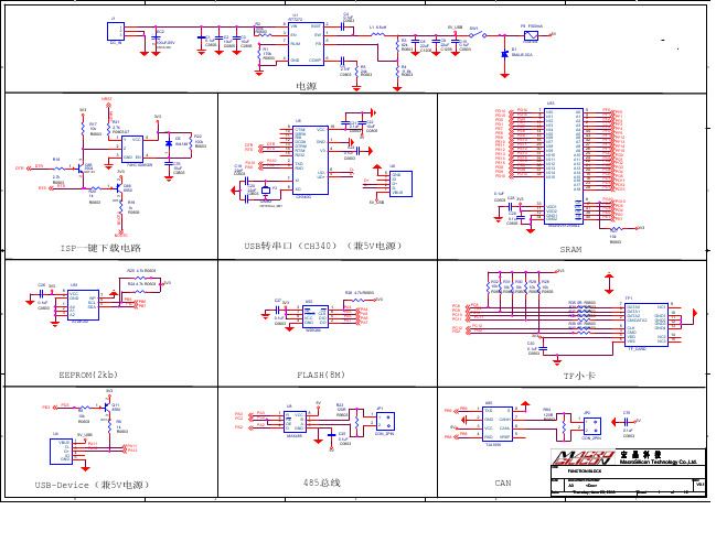
芯嵌stm32开发板原理图V3.0版本

C31 104 R54
PA8 PC8 PA9 PC9 PA10 PC10 PA11 PC11 PA12 PC12 PA13/JTMS/SWDIO PC13-TAMPER-RTC PA14/JTCK/SWCLK PC14-OSC32_IN PA15/JTDI PC15-OSC32_OUT PB0 PB1 PB2/BOOT1 PB3/JTDO PB4/JNTRST PB5 PB6 PB7 PB8 PB9 PB10 PB11 PB12 PB13 PB14 PB15 OSC_IN OSC_OUT BOOT0 NRST VREFVREF+ NC VBAT VDD_1 VDD_2 VDD_3 VDD_4 VDD_5 VDDA STM32F103VET6 C10 PD0 PD1 PD2 PD3 PD4 PD5 PD6 PD7 PD8 PD9 PD10 PD11 PD12 PD13 PD14 PD15 PE0 PE1 PE2 PE3 PE4 PE5 PE6 PE7 PE8 PE9 PE10 PE11 PE12 PE13 PE14 PE15 VSS_1 VSS_2 VSS_3 VSS_4 VSS_5 VSSA
USB
B
USB-SLAVE 1 VCC 2 D3 D+ 4 GND 5 SHL 6 SHL USB-SLAVE
U5V
R41 22 R42 22 R44 1K C41 R43 0.01uF1M Q1
PA11-USBDM PA12-USBDP
stm32开发板原理图
Y5 1 4 3
C41 0.1uF C0603 VGND IOVDD0 IOVDD1 IOVDD2 6 14 19 CVDD CVDD0 CVDD1 CVDD2 CVDD3 RX TX 5 7 24 31 26 27 4 16 20 21 22 35 38 43 45 C35 0.1uF C0603 VGND C36 0.1uF C0603 C37 0.1uF C0603 C38 0.1uF C0603 R43 100k IOVDD R0603
C76 10uF C0805
U6 6 5 DD+ D+ D5 4 3 2 1 GND ID D+ DVBUS
PD14 PD15 PD0 PD1 PE7 PE8 PE9 PE10 PE11 PE12 PE13 PE14 PE15 PD8 PD9 PD10
PD14 PD15 PD0 PD1 PE7 PE8 PE9 PE10 PE11 PE12 PE13 PE14 PE15 PD8 PD9 PD10
5
4
3
2
1
J1 1 2 3 DC_IN R2 100k R0603 C1 0.1uF C0603 C2 10uF C0805 C3 10uF C0805 R1 179k R0603 8 3 7 1
U1 RT7272 VIN EN RLIM B00T SW FB 2 1 5 + EC2 2 100uF/25V
C42 0.01uF C0603R44 22R R0603 C43 0.01uF C0603 RIGHT R45 22R R0603
AGND
C60 18pF C0603
2
R53 1M R0603 30 31
U57 XI/CLKIN XO TXN TXP RXN RXP LINKLED ACTLED NC1 NC2 NC3 NC4 DNC VBG RSVD1 RSVD2 RSVD3 RSVD4 RSVD5 PMODE2 PMODE1 PMODE0 EXRES1 T0CAP 1V20 RSVD 1 2 5 6 25 27 46 47 12 13 7 18 38 39 40 41 42 43 44 45 10 R58 12.4k R0603 4.7uF C0603 0.01uF C0603 AGND R66 10k R0603 R65 10k R0603 AGND R64 10k R0603 R63 10k R0603 R62 10k R0603 R61 10k R0603 3V3 R60 10k R0603 R59 10k R0603 TXN TXP RXN RXP LINKLED ACTLED
stm32常见通信方式(TTL、RS232、RS485、CAN)总结

stm32常见通信方式(TTL、RS232、RS485、CAN)总结
一、TTL电平:全双工(逻辑1: 2.4V--5V 逻辑0: 0V--0.5V)
1、硬件框图如下,TTL用于两个MCU间通信
2、‘0’和‘1’表示
二、RS-232电平:全双工(逻辑1:-15V--5V 逻辑0:+3V--+15V)
1、硬件框图如下,TTL用于MCU与PC机之间通信需要加电平转换芯片
2、‘0’和‘1’表示
三、RS-485:半双工、(逻辑1:+2V--+6V 逻辑0:-6V---2V)这里的电平指AB 两线间的电压差
1、硬件框图如下
2、‘0’和‘1’表示
四、CAN总线:逻辑1:-1.5V--0V 逻辑0:+1.5V--+3V)这里的电平指CAN_High、CAN_Low 两线间的电压差
1、硬件框图如下
2、‘0’和‘1’表示
以上总结:
1、从单片机软件编程角度来说,RS23
2、RS-485最终结果都是转换为TTL电平方式与单片机通信(CAN收发器把差分信号转化为TTL-->CAN控制器(MCU))。
其目的都是提高通信质量,提高抗干扰能力。
2、TTL、RS232是逻辑电平信号。
RS-485、CAN为差分信号。
五、I2C
5.1 I2C物理层
5.2 I2C协议层
5.3 数据的起始信号与停止信号
5.4数据有效性
I2C 协议在SCL 高电平时对SDA 信号采样,SCL 低电平时SDA准备下一个数据。
STM32ADC多通道16路电压信号采集

STM32ADC多通道16路电压信号采集下面介绍一种利用STM32单片机制作的16路多通道ADC采集电路图和源程序。
采用USB接口与电脑连接,实则USB转串口方式,所以上位机可以用串口作为接口。
电路图中利用LM324作为电压跟随器,起到保护单片机引脚的作用。
直接在电脑USB取点,省去外接电源麻烦,实测耗电电流不到20ma.1.主控电路图:2. USB转串口电路图3.LM324电压跟随器电路图4.滤波电路图5.16路接口电路图6.电源电路图7.16路ADC初始化程序:void Adc_Init(void){//先初始化IO口RCC->APB2ENR|=0X7<<2; //使能PORTA\PORAB\PORTC口时钟GPIOA->CRL&=0X00000000;//PA0 1 2 3 4 5 6 7 anolog输入GPIOB->CRL&=0XFFFFFF00;//PB0 1 anolog输入GPIOC->CRL&=0XFF000000;//PC0 1 2 3 4 5 anolog输入//通道10/11设置RCC->APB2ENR|=1<<9; //ADC1时钟使能RCC->APB2RSTR|=1<<9; //ADC1复位RCC->APB2RSTR&=~(1<<9);//复位结束RCC->CFGR&=~(3<<14); //分频因子清零//SYSCLK/DIV2=12M ADC时钟设置为12M,ADC最大时钟不能超过14M!//否则将导致ADC准确度下降!RCC->CFGR|=2<<14;ADC1->CR1&=0XF0FFFF; //工作模式清零ADC1->CR1|=0<<16; //独立工作模式ADC1->CR1&=~(1<<8); //非扫描模式ADC1->CR2&=~(1<<1); //单次转换模式ADC1->CR2&=~(7<<17);ADC1->CR2|=7<<17; //软件控制转换ADC1->CR2|=1<<20; //使用用外部触发(SWSTART) 必须使用一个事件来触发ADC1->CR2&=~(1<<11); //右对齐ADC1->SQR1&=~(0XF<<20);ADC1->SQR1&=0<<20; //1个转换在规则序列中也就是只转换规则序列1//设置通道采样时间ADC1->SMPR2&=0X00000000;//通道0,1,2,3,4,5,6,7,8,9采样时间清空ADC1->SMPR2|=7<<27; //通道9 239.5周期,提高采样时间可以提高精确度ADC1->SMPR2|=7<<24; //通道8 239.5周期,提高采样时间可以提高精确度ADC1->SMPR2|=7<<21; //通道7 239.5周期,提高采样时间可以提高精确度ADC1->SMPR2|=7<<18; //通道6 239.5周期,提高采样时间可以提高精确度ADC1->SMPR2|=7<<15; //通道5 239.5周期,提高采样时间可以提高精确度ADC1->SMPR2|=7<<12; //通道4 239.5周期,提高采样时间可以提高精确度ADC1->SMPR2|=7<<9; //通道3 239.5周期,提高采样时间可以提高精确度ADC1->SMPR2|=7<<6; //通道2 239.5周期,提高采样时间可以提高精确度ADC1->SMPR2|=7<<3; //通道1 239.5周期,提高采样时间可以提高精确度ADC1->SMPR2|=7<<0; //通道0 239.5周期,提高采样时间可以提高精确度ADC1->SMPR1&=0XFFFC0000;//通道10,11,12,13,14,15采样时间清空ADC1->SMPR1|=7<<15; //通道15 239.5周期,提高采样时间可以提高精确度ADC1->SMPR1|=7<<12; //通道14 239.5周期,提高采样时间可以提高精确度ADC1->SMPR1|=7<<9; //通道13 239.5周期,提高采样时间可以提高精确度ADC1->SMPR1|=7<<6; //通道12 239.5周期,提高采样时间可以提高精确度ADC1->SMPR1|=7<<3; //通道11 239.5周期,提高采样时间可以提高精确度ADC1->SMPR1|=7<<0; //通道10 239.5周期,提高采样时间可以提高精确度ADC1->CR2|=1<<0; //开启AD转换器ADC1->CR2|=1<<3; //使能复位校准while(ADC1->CR2&1<<3); //等待校准结束//该位由软件设置并由硬件清除。
STM32开发板原理图
R7
45K DC5V
Y1 C2 22pF
R15 DGND DC3.3V R16 R17
10K 30.PA5-SPI1-SCK 10K 31.PA6-SPI1-MISO 10K 32.PA7-SPI1-MOSI A
DC3.3V C A 8550-PNP Q1 E B
R3 10K R4 1K
104
5 9 4 8 3 7 2 6 1
2.4K
ENC28J60CSS (SSOP-28)
RJ45-HR911105A
1 2 3 4 5 6 7 8
DAT2 CD/DAT3 CMD VDD3V CLK VSS DATA0 DATA1 TF_card
1
DC3.3V
DGND
AT24C02(SO-8)
DC5V
60.PD13-LIGHT-PWM 57.PD10-D15
DB9 DB9RA/F
11
1K
10M以太网
DGND C11 U5 10uF 1 2 3 4 5 6 7 8 9 10 11 12 13 14
SPI1
Vcap Vss CLKO INT WOL SO SI SCK CS RST Vssrx TPINTPIN+ Rbias VDD LEDA LEDB Vddosc OSC2 OSC1 Vssosc Vsspll Vddpll Vddrx Vsstx TPOUT+ TPOUTVddtx DC3.3V 28 C13 103 27 26 25 DC3.3V 24 23 22 21 20 19 18 17 16 15 DGND DC3.3V TPOUT+ R21 TPOUT- R22 DC3.3V RJ 1 DGND 2 LEDA 4 LEDB 8 DGND C17 7 C14 20pF 104 C18 104 5 TPIN+ 3 DGND TPIN6 Y2 DGND R24 1K 9 25MHZ 10 C15 20pF R25 1K 12 L1 11 50 DC3.3V A 50 100nH-0805 B C16 103 DGND DGND TPOUT+ TPOUTTD+ TDGND RD+ RDGLEDA GLEDK YLEDA YLEDK A B
STM32一键下载电路详解
STM32一键下载电路详解
STM32一键下载电路详解
以上就是一键下载电路,mcuisp会控制CH340的RTS#和DTR#高低电平的变化,通过控制高低电平的变化,进而控制BOOT0和RESET的状态,我用电压表测试了引脚电平的状态,RTS#和DTR#初始状态时为高电平,在启用下载的时候,DTR#维持高,RTS#拉低,此时Q2和Q3都导通,那么BOOT0为高电平状态,RESET为低电平复位,然后DTR#变低,Q2不导通,复位结束,此时的BOOT0为高电平,那么就会启用串口下载程序,开始和mcuisp下载软件进行通信,进行代码下载,等到代码下载结束时,RTS#先变高电平,然后DTR#在变高电平,如果DTR#先变到电平,那么又会产生复位的。
STM32处理器的USB接口
STM32处理器的USB接口1、接口模块的内部结构在书上有一个很好的USB内部接口模块内部结构图,比较好的解释了各个模块之间的关系,我这里试着用我自己的理解阐述一下吧。
首先在总线端(与D+、D-相连的那一端),通过模拟收发器与SIE连接。
SIE使用48MHz的专用时钟。
与SIE相关的的有三大块:CPU内部控制、中断和端点控制寄存器,挂起定时器(这个好像是USB协议的要求,总线在一定时间内没有活动,SIE模块能够进入SUSPEND状态以节约电能),还有包缓冲区接口模块。
说到包缓冲区接口模块,这个对应的含义是,USB设备应该提供USB包缓冲区。
这块缓冲区同时受到SIE和CPU核心的控制,用于CPU与SIE共享达到数据传输的目的。
所以CPU通过APB1总线接口访问,SIE通过包缓冲区接口模块访问,中间通过Arbiter来协调访问。
当然我们关注的中心点是控制、中断和端点控制寄存器。
我们通过这些寄存器来获取总线传输的状态,控制各个端点的状态,并可以产生中断来让CPU处理当前的USB事件。
CPU可以通过APB1总线接口来访问这些寄存器。
它们使用的都是PCLK1时钟。
2、USB模块的寄存器认识(1)控制寄存器CNTR(2)中断状态寄存器ISTR这个寄存器主要是反映USB模块当前的状态的。
第15-8为与控制寄存器的中断允许是意义对应的。
相应的标志位置位,且中断未屏蔽,则向CPU发出对应的中断。
(3)USB设备地址寄存器第7位,EF,USB模块允许位。
如果EF=0,则USB模块将停止工作。
第6-0位。
USB当前使用的地址。
复位时为0.(4)端点状态和配置寄存器,8个寄存器,支持8个双向端点和16个单向端点。
(5)端点描述符表相关寄存器首先有一个描述符表地址寄存器,指明了包缓冲区内端点描述符表的地址。
每一个端点都对应一个描述附表。
描述符表也在包缓冲区内。
每个端点寄存器对应的描述符表的地址可根据公式计算。
单缓冲、双向的端点描述符表有四项,每项占据两个字节:分别是端点n的发送缓冲区地址、发送字节数、接收缓冲区地址、接收字节数。
STM32串口
STM32串口通讯班级:100714姓名:孙小军学号:10071037一、设计要求用STM32设计一个与计算机进行串口通讯的实验,要求STM32在接收到计算机发来的数据时进行+1操作,并且将数据返回给计算机,可以利用中断和查询两种方式,画出STM32与计算机RS232通讯的电路图,画出程序流程图,写出程序代码(STM32内部子函数)以及代码注释。
二、电路原理图原理图分析:本原理图采用STM32的串口通过MAX232电平转换芯片与计算机RS232口相连接。
其中STM32只给出了串口1的引脚示意图(本实验只用到串口1)。
三、程序流程图四、程序代码及注解#include “stm32f10x.h”voidRCC_Configuration(void);voidGPIO_Configuration(void);voidUSART_Configuration(void);int main(){u32i=0;u32 number=0;RCC_Configuration();//设置系统时钟GPIO_Configuration();//设置GPIO端口USART_Configuration();//设置串口while(1){/*等待串口1接收数据完毕*/If(USART_GetFlagStatus(USART1,USART_IT_RXNE)==SET){/*向串口发送接收到的数据*/USART_SendData(USART1,USART_ReceiveData(USART1));for(i=0;i<100;i++);//延时保证接收发送稳定性number++;//记录接收数据次数}}}/*时钟初始化子程序*//*开启USART1和GPIOA时钟*/voidRCC_Configuration(void){ErrorStatusHSEStartUpStatus;RCC_DeInit();RCC_HSEConfig(RCC_HSE_ON);HESEStartUpStatus=RCC_WaitForHSEStartUp();if(HSEStartUpStatus==SUCCESS){RCC_HCLKConfig(RCC_SYSCLK_Div1);RCC_PCLK2Config(RCC_HCLK_Div1);RCC_PCLK1Config(RCC_HCLK_Div2);FLASH_SetLatency(FLASH_PrefetchBuffer_Enable);RCC_PLLConfig(RCC_PLLSource_HSE_Div1,RCC_PLLMul_9);RCC_PLLCmd(ENABLE);while(RCC_GetFlagStatus(RCC_FLAG_PLLRDY)==RESET);RCC_SYSCLKConfig(RCC_SYSCLKSource_PLLCLK);while(RCC_GetSYSCLKSource()!=0x80);}RCC_APB2PeriphClockCmd(RCC_APB2Periph_USART1|RCC_APB2Periph_GPIO,ENABLE);}/*GPIO初始化子程序*/voidGPIO_Configuration(void){GPIO_InitTypeDefGPIO_InitStructure;GPIO_InitStructure.GPIO_Pin=GPIO_Pin_9;GPIO_InitStructure.GPIO_Mode=GPIO_Mode_AF_PP;//设置USART1的Tx脚为第二功能推挽式输出模式GPIO_InitStructure.GPIO_Speed=GPIO_Speed_50MHz;GPIO_Init(GPIOA,&GPIO_InitStructure);GPIO_InitStructure.GPIO_Pin=GPIO_Pin_10;GPIO_InitStructure.GPIO_Mode=GPIO_Mode_IN_FLOATING;//设置USART1的Rx脚为浮空输入脚GPIO_Init(GPIOA,&GPIO_InitStructure);}voidUSART_Configuration(void){USART_InitTypeDefUSART_InitStructure;USART_ClockInitTypeDefUSART_ClockInitStructure;/*波特率为9600bps,8位数据长度,1个停止位,无奇偶校验位*/ USART_ART_BaudRate=9600;USART_ART_WordLength=USART_WordLength_8b;USART_ART_StopBits=USART_StopBits_1;USART_ART_Parity=USART_Parity_No;USART_ART_HardwareFlowControl=USART_Hardwar eFlowControl_None;USART_ART_Mode=USART_Mode_Rx|USART_Mode _Tx;USART_Init(USART1,&USART_InitStructure);USART_Cmd(USART1,ENABLE);//使能USART1}程序分析:本程序的核心语句在于串口的接收和发送语句,用if判断句来判断是否接收到数据,通过读取标志位来判断若是接收到数据则向PC发送接收到的数据,程序思路简单,只需要一下几步即可完成:1.配置RCC寄存器组,使用PLL输出72MHz时钟并且作为主时钟源;2.配置GPIOA端口,设置GPIOA.9为第二功能推挽式输出模式,GPIOA.10为浮空输入模式;3.配置USART设备,主要参数为使用9600bps波特率,8位数据长度,1个停止位,无奇偶校验位,全双工无硬件流控制。