电子信息专业外文翻译---EDA的发展及VHDL的应用
EDA技术及软件外文翻译
EDA Technology And SoftwareEDA is Electronic Design Automation (Electronic Automation) is the abbreviation of themselves, in the early 1990s from computer aided Design (CAD), computer aided manufacturing (CAM), computer aided testing (CAT) and computer aided engineering (CAE) development of the concepts and come.EDA technology is on the computer as the tool, the designer in EDA software platform, with VHDL HDL finish design documents, then by the computer automatically logic compilation, reduction, division, comprehensive, optimization, layout and wiring and simulation for a particular goal chips, until the adapter compilation, logic mapping and programming download, etc.1 EDA technology conceptsEDA technology is in electronic CAD technology developed on the basis of computer software system by means of computer for working platform, shirt-sleeve application of electronic technology, computer technology and information processing and intelligent technology to the latest achievements of electronic products, the automatic design.Using EDA tools, electronic stylist can be from concept, algorithm, agreement, etc, begin to design your electronic system a lot work can be finished by computer and electronic products can be from circuit design, performance analysis to design the IC territory or PCB layout the whole process of the computer automatically complete the processing.Now on the concept of using EDA or category very wide. Included in machinery, electronics, communication, aerospace, chemical, mineral, biology, medicine, military and other fields, have EDA applications. Current EDA technology has in big companies, enterprises, institutions and teaching research departments extensive use. For example in the aircraft manufacturing process, from design, performance testing and characteristic analysis until a flight simulator, all may involve EDA technology. Globalization-the EDA technology, mainly in electronic circuit design, PCB design and IC design.EDA can be divided into system level and circuit-level and physical implementation level.2. Development Environment MAX + PLUSⅡ/ QUARTERⅡAltera Corporation is the world's three major CPLD / FPGA manufacturers of the devices it can achieve the highest performance and integration, not only because of the use of advanced technology and new logic structure, but also because it provides a modern design tools MAX + PLUSⅡprogrammable logic development software, the software is launched the third generation of Altera PLD development system. Nothing to do with the structure provides a design environment for Altera CPLD designers to easily design entry, quick processing, and device programming. MAX + PLUSⅡprovides a comprehensive logic design capabilities, including circuitdiagrams, text and waveform design entry and compilation, logic synthesis, simulation and timing analysis, and device programming, and many other features. Especially in the schematic so, MAX + PLUSⅡis considered the most easy to use, the most friendly man-machine interface PLD development software. MAX + PLUSⅡcan develop anything other than the addition APEX20K CPLD / FPGA.MAX + PLUSⅡdevelopment system has many outstanding features:① open interface.②design and construction related: MAX + PLUSⅡsupport Altera's Classic, ACEX 1K, MAX 3000, MAX 5000, MAX 7000, MAX 9000, FLEX 6000, FLEX 8000 and FLEX 10K series of programmable logic devices, gate count is 600 ~ 250 000 doors, offers the industry really has nothing to do with the structure of programmable logic design environment. MAX + PLUSⅡcompiler also provides a powerful logic synthesis and optimization to reduce the burden on the user's design.③can be run on multiple platforms: MAX + PLUSⅡsoftware PC-based WindowsNT 4.0, Windows 98, Win dows 2000 operating systems, but also in Sun SPARCstations, HP 9000 Series 700/800, IBM RISC System/6000 such as run on workstations.④fully integrated: MAX + PLUSⅡsoftware design input, processing, calibration functions are fully integrated within the programmable logic development tools, which can be debugged more quickly and shorten the development cycle.⑤modular tools: designers can input from a variety of design, editing, calibration and programming tools to choose the device to form a user-style development environment, when necessary, to retain on the basis of the original features to add new features. The MAX + PLUSⅡSeries supports a variety of devices, designers need to learn new development tools for the development of new device structures.⑥mail-description language (HDL): MAX + PLUSⅡsoftware supports a variety of HDL design entry, including the standard VHDL, V erilog HDL and Altera's own developed hardware description language AHDL.⑦MegaCore Function: MegaCore are pre-validated for the realization of complex system-level functions provided by the HDL netlist file. It ACEX 1K, MAX 7000, MAX 9000, FLEX 6000, FLEX 8000 and FLEX 10K devices provide the most optimal design. Users can purchase them from the Altera MegaCore, using them can reduce the design task, designers can make more time and energy to improve the design and final product up.⑧ OpenCore Features: MAX + PLUSⅡsoftware with open characteristics of the kernel, OpenCore come to buy products for designers design their own assessment.At the same time, MAX + PLUSⅡthere are many other design entry methods, including:①graphic design input: MAX + PLUSⅡgraphic design input than other software easier to use features, because the MAX + PLUSⅡprovides a rich library unit for the designer calls, especially in the MAX2LIB in the provision of the mf library includes almost all 74 series of devices, in the prim library provides all of the separate digital circuit devices. So long as a digital circuit knowledge, almost no learning can take advantage of excess MAX + PLUSⅡfor CPLD / FPGA design. MAX + PLUSⅡalso includes a variety of special logic macros (Macro-Function) andthe parameters of the trillion of new features (Mega-Function) module. Full use of these modules are designed to greatly reduce the workload of designers to shorten design cycles and multiply.②Enter the text editor: MAX + PLUSⅡtext input language and compiler system supports AHDL, VHDL language, VERILOG language of the three input methods.③ wave input: If you know the input, output waveform, the waveform input can also be used.④hybrid approach: MAX + PLUSⅡdesign and development environment for graphical design entry, text editing input, waveform editing input hybrid editing. To do: in graphics editing, wave form editing module by editing the text include "module name. Inc" or the use of Function (... ..) Return (....) Way call. Similarly, the text editing module input form can also be called when the graphics editor, AHDL compiler results can be used in the VHDL language, VHDL compiler of the results can also be entered in the AHDL language or graphic to use. This flexible input methods, to design the user has brought great convenience.Altera's QuartusⅡis a comprehensive PLD development software to support the schematic, VHDL, V erilog HDL, and AHDL (Altera Hardware Description Language) and other design input forms, embedded devices, and integrated its own simulator, you can complete the design input to complete the hardware configuration of the PLD design process.QuartusⅡin the XP, Linux and Unix on the use, in addition to using the Tcl script to complete the design process, to provide a complete graphical user interface design. With running speed, unified interface, feature set, easy to use and so on.Altera's QuartusⅡsupport IP core, including the LPM / MegaFunction macro function module library, allowing users to take full advantage of sophisticated modules, simplifying the design complexity and speed up the design speed. Good for third-party EDA tool support also allows the user to the various stages in the design process using the familiar third-party EDA tools.In addition, QuartusⅡand DSP Builder tools and by Matlab / Simulink combination, you can easily achieve a variety of DSP applications; support Altera's programmable system chip (SOPC) development, set system-level design, embedded software development, programmable logic design in one, is a comprehensive development platform.MaxPLUSⅡgeneration as Altera's PLD design software, due to its excellent ease of use has been widely used. Altera has now stopped MaxPLUSⅡupdate support, QuartusⅡnot only support the device type as compared to the rich and the graphical interface changes. Altera QuartusⅡincluded in many such SignalTapⅡ, Chip Editor and RTL Viewer design aids, integrated SOPC and HardCopy design process, and inherit MaxPLUSⅡfriendly graphical interface and easy to use.MaxPLUSⅡgeneration as Altera's PLD design software, due to its excellent ease of use has been widely used. Altera has now stopped MaxPLUSⅡupdate support, QuartusⅡnot only support the device type as compared to the rich and the graphical interface changes. Altera QuartusⅡincluded in many such SignalTapⅡ, Chip Editor and RTL Viewer design aids, integrated SOPC and HardCopy design process, and inherit MaxPLUSⅡ friendly graphical interface and easy to use.Altera QuartusⅡ as a programmable logic design environment, due to its strong design capabilities and intuitive interface, more and more digital systems designers welcome.Altera's QuartusⅡis the fourth generation of programmable logic PLD software development platform. The platform supports a working group under the design requirements, including support for Internet-based collaborative design. Quartus platform and Cadence, ExemplarLogic, MentorGraphics, Synopsys and Synplicity EDA vendors and other development tools are compatible. LogicLock improve the software module design features, added FastFit compiler options, and promote the network editing performance, and improved debugging capabilities. MAX7000/MAX3000 devices and other items to support the product.3. Development of language VHDLVHDL (V ery High Speed Integrated Circuit Hardware Description Language) is a very high speed integrated circuit hardware description language, it can describe the function of the hardware circuitry, signal connectivity and the time between languages. It can be more effective than the circuit diagram to express the characteristics of the hardware circuit. Using the VHDL language, you can proceed to the general requirements of the system, since the detailed content will be designed to come down to earth, and finally to complete the overall design of the system hardware. IEEE VHDL language has been the industry standard as a design to facilitate reuse and sharing the results. At present, it can not be applied analog circuit design, but has been put into research. VHDL program structure, including: entity (Entity), structure (Architecture), configure (Configuration), Package Collection (Package) and the Library (Library). Among them, the entity is the basic unit of a VHDL program, by entity and the structure of two parts: the physical design system that is used to describe the external interface signal; structure used to describe the behavior of the system, the system processes or system data structure form. Configuration select the required language from the library system design unit to form different versions of different specifications, so that the function is designed to change the system. Collection of records of the design module package to share the data types, constants, subroutines and so on. Database used to store the compiled entities, the body structure, including the collection and configuration: one is the development of engineering software user, the other is the manufacturer's database.VHDL, the main features are:① powerful, high flexibility: VHDL language is a powerful language structure, clear and concise code can be used to design complex control logic. VHDL language also supports hierarchical design, support design databases and build re usable components. Currently, VHDL language has become a design, simulation, synthesis of standard hardware description language.② Device independence: VHDL language allows designers to generate a design do not need to first select a specific device. For the same design description, you can use a variety of different device structures to achieve its function. So the design description stage, able to focus on design ideas. When the design, simulation, after the adoption of a specific device specified integrated, adapter can be.③Portability: VHDL language is a standard language, so the use of VHDL design can be carried out by different EDA tool support. Transplanted from one toanother simulation tools simulation tools, synthesis tools from a port to another integrated tool, from a working platform into another working platform. EDA tools used in a technical skills, in other tools can also be used.④top-down design methods: the traditional design approach is bottom-up design or flat design. Bottom-up design methodology is to start the bottom of the module design, the gradual formation of the functional modules of complex circuits. Advantage of this design is obvious because it is a hierarchical circuit design, the general circuit sub-module are in accordance with the structure or function of division, so the circuit level clear, clear structure, easy people to develop, while the design archive file is easy, easy communication. Bottom-up design is also very obvious shortcomings, the overall design concept is often not leaving because the cost of months of low-level design in vain. Flat design is a module containing only the circuit, the circuit design is straightforward and, with no division structure and function, it is not hierarchical circuit design. Advantages of small circuit design can save time and effort, but with the increasing complexity of the circuit, this design highlights the shortcomings of the abnormal changes. Top-down design approach is to design top-level circuit description (top model), and then the top-level simulation using EDA software, if the top-level design of the simulation results meet the requirements, you can continue to lower the top-level module by the division level and simulation, design of such a level will eventually complete the entire circuit. Top-down design method compared with the first two are obvious advantages.⑤ rich data types: as a hardware description language VHDL data types are very rich language, in addition to VHDL language itself dozens of predefined data types, in the VHDL language programming also can be user-defined data types. Std_logic data types in particular the use of VHDL language can make the most realistic complex signals in analog circuits.⑥ modeling convenience: the VHDL language can be integrated in the statement and the statement are available for simulation, behavior description ability, therefore particularly suitable for signal modeling language VHDL. The current VHDL synthesizer to complex arithmetic comprehensive descriptions (such as: Quartus Ⅱ2.0 and above versions of std_logic_vector type of data can add, subtract, multiply, divide), so the circuit modeling for complex simulation of VHDL language, whether or comprehensive description of the language are very appropriate.⑦rich runtime and packages: The current package supports VHDL, very rich, mostly in the form of libraries stored in a specific directory, the user can at any time. Such as the IEEE library collection std_logic_1164, std_logic_arith, std_logic_unsigned other package. In the CPLD / FPGA synthesis, EDA software vendors can also use the various libraries and provide package. VHDL language and the user using a variety of results can be stored in a library, in the design of the follow-up can continue to use.⑧VHDL language is a modeling hardware description language, so with ordinary computer languages are very different, common computer language is the CPU clock according to the beat, after an instruction to perform the next instruction, so instruction is a sequential, that is the order of execution, and execution of each instruction takes a specific time. VHDL language to describe the results with the corresponding hardware circuit, which follows the characteristics of hardware, there isno order of execution of the statement is executed concurrently; and statements that do not like ordinary software, take some time each instruction, just follow their own hardware delay.EDA技术及软件EDA是电子设计自动化(Electronic Design Automation)的缩写,在20世纪90年代初从计算机辅助设计(CAD)、计算机辅助制造(CAM)、计算机辅助测试(CAT)和计算机辅助工程(CAE)的概念发展而来。
EDA技术与VHDL程序开发基础教程_教学资料_第一章

1.8.1填空1.EDA的英文全称是Electronic Design Automation2.EDA技术经历了计算机辅助设计CAD阶段、计算机辅助工程设计CAE阶段、现代电子系统设计自动化EDA阶段三个发展阶段3. EDA技术的应用可概括为PCB设计、ASIC设计、CPLD/FPGA设计三个方向4.目前比较流行的主流厂家的EDA软件有Quartus II、ISE、ModelSim、ispLEVER5.常用的设计输入方式有原理图输入、文本输入、状态机输入6.常用的硬件描述语言有VHDL、Verilog7.逻辑综合后生成的网表文件为EDIF8.布局布线主要完成将综合器生成的网表文件转换成所需的下载文件9.时序仿真较功能仿真多考虑了器件的物理模型参数10.常用的第三方EDA工具软件有Synplify/Synplify Pro、Leonardo Spectrum11.2000年推出的Pentium4微处理器芯片的集成度达(4200 )万只晶体管。
12.在EDA发展的(CAD )阶段,人们只能借助计算机对电路进行模拟、预测,以及辅助进行集成电路版图编辑、印刷电路板(PCB)布局布线等工作。
13.在EDA发展的(CAE )阶段,人们可以将计算机作为单点设计工具,并建立各种设计单元库,开始用计算机将很多单点工具集成在一起使用。
14.EDA设计输入主要包括图形输入、HDL文本输入和状态机输入。
15.时序仿真是在设计输入完成之后,选择具体器件并完成布局、布线之后进行的时序关系仿真,因此又称为功能仿真。
16.VHDL的数据对象包括变量、常量和信号,它们是用来存放各种类型数据的容器。
17.图形文件设计结束后一定要通过仿真,检查设计文件是否正确。
18.以EDA方式设计实现的电路设计文件,最终可以编程下载到FPGA 和CPLD芯片中,完成硬件设计和验证。
19.MAX+PLUS的文本文件类型是(后缀名).VHD 。
20.在PC上利用VHDL进行项目设计,不允许在根目录下进行,必须在根目录为设计建立一个工程目录(即文件夹)。
EDA技术的应用及发展
EDA技术的应用及发展作者:张晓霞来源:《中国新技术新产品》2012年第10期摘要:EDA技术给电子系统设计和生产带来了革命性的变化,本文介绍了EDA技术的发展史,将EDA系统设计方法与传统电子设计方法进行比较,分析了EDA技术应用及未来的发展趋势。
关键词:EDA技术;应用;发展趋势中图分类号:TN4 文献标识码:A随着微电子技术的迅猛发展,现代电子产品的性能提高、集成度和精密度不断的增加,电子产品更新换代的节奏越来越快。
采用传统的电子设计方法设计电路越来越困难,EDA技术提高了电路的设计效率和可靠性,减少了劳动强度,给电子系统设计带来了革命性的变化。
1 EDA技术EDA是电子设计自动化(Electronics Design Automation)的缩写,EDA技术是指以计算机为工作平台,融合了应用电子技术、计算机技术、信息处理技术及智能化技术的最新成果,进行电子产品的自动设计。
EDA技术的发展经历了三个阶段:①20世纪70年代,交互设计,解决晶体管级版图设计及PCB布局布线;②20世纪80年代初,功能包括逻辑图设计输入、仿真、自动布局布线和难,设计层次从版图级上升到原理图级,设计效率提高了10倍以上次;③20世纪80年代后期,增加了VHDL硬件描述语言输入、仿真和逻辑功能综合(RTL级),EDA技术从电路级上升到系统设计。
随着系统变得复杂和庞大,EDA系统设计工具的出现为系统设计师们提供了优越的环境和有力的保障。
EDA技术与传统电子设计相比在产品设计理念、设计方式、系统硬件构成和知识产权等方面更具优势。
图1对EDA设计与传统设计流程进行比较。
图1 传统电子设计与EDA设计流程的比较EDA系统设计采用的是自上而下的设计方法,符合设计人员的设计思路,从功能描述开始,到物理实现。
系统设计者逐步从使用硬件转向设计硬件、从单个电子产品开发转向系统电子产品开发。
EDA技术集设计、仿真、测试于一体,配置了系统设计自动化的全部工具。
配套课件 EDA技术与VHDL程序设计基础教程

它支持原理图、VHDL和Verilog 语言文本输入方式和波形或EDIF 格式的文件作为输入,且支持这 些文件的混合设计。
Quartus II的GUI界面
EDA技术与VHDL程序开发基础教程
五、EDA集成开发工具
ISE+ModelSim
ispLEVER
EDA技术与VHDL程序开发基础教程
。(b)中三条竖线A、B、C也为输入线,输入到或门的横线为和线。和线与
输入线的交叉点为编程点。
当输入线与和线相连通时,
在编程点处以“×”表示。
Y=AB
可以看出,图中电路表示
Y=A+B+C
的逻辑表达式分别为Y=AB
和Y=A+B+C。
ABC
ABC
(a)
(b)
EDA技术与VHDL程序开发基础教程
三、 CPLD的基本结构和工作原理
EDA技术与VHDL程序开发基础教程
第1章 EDA概述
重点内容:
EDA技术发展和应用 EDA工程设计流程 EDA集成开发工具
EDA技术与VHDL程序开发基础教程
一、EDA工程简介
EDA(Electronic Design Automation)工程是现代电子信息工程领 域中一门发展迅速的新技术。
流程
需求分析
算法设计 (Algorithm Optimization)
构架设计 (Architecture Exploration)
RTL 设计 (RTL Design)
RTL 验证 (RTL Verification)
综合 (Synthesis)
门级验证 (Gate-level Verification)
EDA技术及其应用

1.9 硬件测试技术
1.9.2 JTAG边界扫描测试
表1-1 边界扫描IO引脚功能
引脚
描述
功能
TDI 测试数据输入(Test Data Input) TDO 测试数据输出(Test Data Output)
测试指令和编程数据的串行输入引脚。数据在TCK的上升沿移 入。
测试指令和编程数据的串行输出引脚,数据在TCK的下降沿移 出。如果数据没有被移出时,该引脚处于高阻态。
适配器件
Timing Analyzer (时序分析器)
仿真
编程器
下载
图1-19 Quartus II设计流程
1.14 IP核
IP
软IP
固IP
硬IP
用HDL等硬件描述语 言描述的功能块,但 是并不涉及用什么具 体电路元件实现这些 功能。
完成了综合 的功能块
提供设计的 最终阶段产 品:掩膜
1.15 EDA的发展趋势
1.1 EDA技术
EDA (Electronic Design Automation)
EDA技术就是依赖功能强大的计算机,在EDA工具软件 平台上,对以硬件描述语言HDL (Hardware Description Language)为系统逻辑描述手段完成的设计文件,自动地完 成逻辑编译、化简、分割、综合、布局布线以及逻辑优化和 仿真测试,直至实现既定的电子线路系统功能。
随着市场需求的增长,集成工艺水平及计算机自动设 计技术的不断提高,促使单片系统,或称系统集成芯片成 为IC设计的发展方向
随着系统开发对EDA技术的目标器件各种性能要求的 提高,ASIC和FPGA将更大程度相互融合。
现在,传统ASIC和FPGA之间的界限正变得模糊。系 统级芯片不仅集成RAM和微处理器,也集成FPGA。整个 EDA和IC设计工业都朝这个方向发展,这并非是FPGA与 ASIC制造商竞争的产物,而对于用户来说,意味着有了更 多的选择。
EDA基础总结
E D A基础总结综述部分1.EDA的中文全称为电子设计自动化,英文全名为Electronic Design Automation;2.EDA平台常用的两种输入电路的方法是:电路原理图输入法、HDL输入法;3.EDA平台工作流程:电路输入、综合优化、功能仿真、布局布线、门级仿真;数字电路部分1.EDA中常用的仿真语言为Verilog和VHDL;2.VHDL其英文全名为VHSIC Hardware Description Language,而VHSIC则是Very HighSpeed Intergeraterd Circuit的缩写词,意为甚高速集成电路,故VHDL其准确的中文译名为甚高速集成电路的硬件描述语言;3.Verilog HDL其英文全名为Verilog Hardware Decription Language,HDL中文译名为硬件描述语言;4.Verilog和VHDL的比较共同点:能形式化地抽象表示电路的行为和结构;支持逻辑设计中层次与范围的描述;可借用高级语言的精巧结构来简化电路行为的描述;具有电路仿真与验证机制以保证设计的正确性;支持电路描述由高层到低层的综合转换;硬件描述与实现工艺无关;便于文档管理;易于理解和设计重用;不同点:Verilog在系统级抽象方面略差,VHDL在门级开关电路方面略差;5.软核、固核和硬核软核:功能经过验证的、可综合的、实现后电路结构总门数在5000门以上的Verilog 模型;固核:在某一种现场可编程门列器件上实现的经验证是正确的,且总门数在5000门以上的电路结构编码文件;硬核:在某一种专用集成电路工艺的器件上实现的,经验证是正确的,且总门数在5000门以上的电路结构版图掩膜;6.自顶向下Top Down设计7.自底向上Down Top设计8.名词解释:ASIC:Application Specific Integrated Circuit,专用集成电路;FPGA:Field Programmable Gate Array,现场可编程门阵列;PLD:Programmable Logic Device,可编程逻辑器件;Verilog编程题:数据比较器2位//数据比较器module compare equal, a, b;input a,b;output equal;reg equal;always a or bif a == bequal = 1;elseequal = 0;endmodule//数据比较器测试代码`timescale 1ns/1ns`include "./1-1.v"module t;reg a,b;wire equal;initialbegina=0;b=0;100 a=0; b=1;100 a=1; b=1;100 a=1; b=0;100 a=0; b=0;100 $stop;endcompare m.equalequal, .aa, .bb; endmodule数据比较器8位module compare8equal, a, b;input 7:0a, b;output equal;reg equal;always a or bif a > bbeginequal = 1;endelsebeginequal = 0;endendmodule分频器module half_clkreset, clk_in, clk_out; input clk_in, reset;output clk_out;reg clk_out;always posedge clk_inbeginifreset clk_out = 0;else clk_out = ~clk_out;endendmodule10M时钟分频为500Kmodule fdivision RESET, MB, KB;input MB, RESET;output KB;reg KB;reg 7:0 j;always posedge MBif RESETbeginKB <= 0;j <= 0;endelsebeginif j == 19begin j <= 0;KB <= ~KB;endelsej <= j+1;endendmodule译码电路`define plus 3'd0`define minus 3'd1`define band 3'd2`define bor 3'd3`define unegate 3'd4module aluout, opcode, a, b;output7:0 out;reg7:0 out;input2:0 opcode;input7:0 a,b;always opcode or a or bbegincaseopcode`plus: out = a + b;`minus: out = a - b;`band: out = a & b;`bor: out = a | b;`unegate: out = ~a;default: out = 8'hx;endcaseendendmodule八路数据选择器module selecting8addr, in1, in2, in3, in4, in5, in6, in7, in8, dataout, reset; input 2:0 addr;input 3:0 in1,in2,in3,in4,in5,in6,in7,in8;input reset;output 3:0 dataout;reg 3:0 dataout;always addr or in1 or in2 or in3 or in4 or in5 or in6 or in7 or in8 or reset beginifresetcaseaddr3'b000: dataout = in1;3'b001: dataout = in2;3'b010: dataout = in3;3'b011: dataout = in4;3'b100: dataout = in5;3'b101: dataout = in6;3'b110: dataout = in7;3'b111: dataout = in8;endcaseelsedataout = 0;endendmodule逻辑运算电路module tryfunctclk, n, result, reset;output31:0 result;input3:0 n;input reset, clk;reg31:0 result;always posedge clkbeginif resetresult <=0;elsebeginresult <= nfactorialn/n2+1;endendfunction 31:0 factorial;input 3:0 operand;reg 3:0 index;beginfactorial = operand 1:0;for index = 2; index <= operand; index = index + 1 factorial = index factorial;endendfunctionendmodulemodule tryfunctclk, n, result, reset;output31:0 result;input3:0 n;input reset, clk;reg31:0 result;always posedge clkbeginif resetresult <=0;elsebeginresult <= nfactorialn/n2+1;endendfunction 31:0 factorial;input 3:0 operand;reg 3:0 index;beginfactorial = operand 1:0;for index = 2; index <= operand; index = index + 1 factorial = index factorial;endendfunctionendmodule高速排序组合逻辑module sort4ra, rb, rc, rd, a, b, c, d;output3:0 ra, rb, rc, rd;input3:0 a, b, c, d;reg3:0 ra, rb, rc, rd;reg3:0 va, vb, vc, vd;always a or b or c or dbegin{va, vb, vc, vd} = {a, b, c, d};sort2va, vc;sort2vb, vd;sort2va, vb;sort2vc, vd;sort2vb, vc;{ra, rb, rc, rd} = {va, vb, vc, vd};endtask sort2;input3:0x, y;reg3:0 tmp;if x > ybegintmp = x;x = y;y = tmp;endendtaskendmodule检测5位二进制序列10010module seqdetx, z, clk, rst, state;input x, clk, rst;output z;output2:0 state;reg2:0 state;wire z;parameter IDLE = 'd0, A = 'd1, B = 'd2, C = 'd3, D = 'd4, E = 'd5, F = 'd6, G = 'd7; assign z = state == E && x == 0 1:0;always posedge clkif rstbeginstate <= IDLE;endelsecase stateIDLE:if x == 1beginstate <= A;endA:if x == 0beginstate <= B;endB:if x == 0beginstate <= C;endelsebeginstate <= F;endC:if x == 1beginstate <= D;endelsebeginstate <= G;endD:if x == 0beginstate <= E;endelsebeginstate <= A;endE:if x == 0beginstate <= C;endelsebeginstate = A;endF:if x == 1beginstate <= A;endelsebeginstate <= B;endG:if x == 1beginstate <= F;enddefault:state = IDLE;endcaseendmodule模拟电路部分1.目前,集成电路最常用的材料是单晶硅;2.集成电路的生产由设计、制造、封装三部分组成;3.集成电路中基片主要制作工艺为:光刻、扩散、注入、刻蚀、键合;4.集成电路中基片的制造步骤为:光刻、扩散、注入、刻蚀;5.衡量集成电路产业水平的两个主要参数为:硅晶圆片直径和光刻精度特征尺寸;这两个参数在业界达到的水平为:硅晶圆片直径12英寸300mm,光刻精度0.13um;主流水平为:硅晶圆片直径200mm,光刻精度0.18um;6.模拟电路中常用的仿真算法是SPICE,英文全名为Simulation Program with IntegratedCircuit Emphasis;7.世界上设计EDA软件实力最强的两个公司为Cadence和Synopsys;其中,Cadence的优势为电路布局布线,Synopsys的优势为逻辑综合仿真;8.WorkBench是加拿大IIT公司推出的电子线路仿真软件;它可以对模拟、数字和模拟/数字混合电路进行仿真,克服了传统电子产品的设计受实验室客观条件限制的局限性,用虚拟的元件搭接各种电路,用虚拟的仪表进行各种参数和性能指标的测试;特点如下:1系统集成度高,界面直观,操作方便;2具备模拟、数字及模拟/数字混合电路仿真;3提供较为丰富的元器件库;4电路分析手段完备;5输出方式灵活;6兼容性好;9.SPICE语言举例:EXAMPLE 文件名任意名都可以但必须要有VCC 8 0 12 电源正极接于节点8 负极接于0 电压为12VVEE 0 9 12 电源正极接于节点0,负接接于节点9,电压为12V;VIN 1 0 AC 1 SIN0 0.1 5MEG 信号源VIN 接于1 和接点0;交流1V 进行交流分析同时加一个正弦信号直流偏置为0,振幅为0.1V频率为5M的交流信号源,进行瞬态分析; RC1 8 4 10K 电阻RC1 分别接于节点8 节点4;阻值为10K;RC2 8 5 10K 电阻RC2 分别接于节点8 节点5;阻值为10K;RS 2 1 1K 电阻RS 分别接于节点 1 节点0;阻值为1K;RS1 8 7 20K 电阻RS1 分别接于节点8 节点7 阻值为20K;RS2 3 0 1K 电阻RS2 分别接于节点3 节点0 阻值为1K;Q1 4 2 6 MOD1 三极管Q1 CBE 分别接于节点 4 2 6 模型为MOD1Q2 5 3 6 MOD1 三极管Q2 CBE 分别接于节点 5 3 6 模型为MOD1Q3 6 7 9 MOD1 三极管Q3 CBE 分别接于节点 6 7 9 模型为MOD1Q4 7 7 9 MOD1 三极管Q4 CBE 分别接于节点 7 7 9 模型为MOD1.OP 求出直流工作点.本电路共有9个节点;温度值为27度;.DC VIN -.15 .15 .01 DC为直流分析语句,分析输入电压从-0.15V 到0.15V扫描特性,每0.1V作一次分析;.PRINT DC V4 V5 .PRINT 为打印语句,其中DC是打印直流内容,这里规定打印节点4和5上的电位,既相对地参考点的电压随输入的变化关系;.PLOT DC V4 V5 .PLOT为绘图语句,其中DC表示绘制直流分析的传输特性,说明是绘制V4 V5的输出电压和VIN关系曲线;.TF V5 VIN .TF是转移函数分析语句,该句表示计算直流分析时,小信号输出电压V5和输入电压VIN的转移函数值,输入电阻和输出电阻;.AC DEC 10 25K 250MEG .AC是交流分析语句,是在规定的频率范围内从25K到250M进行频域分析DEC表示按数量级变化,10表示每一数量级中取的分析点数目; .PRINT AC VM5 VP5 打印AC分析VM5VP5的取点数;.PLOT AC VM5 VP5 绘制AC分析VM5VP5的取点数;.TRAN 4N 100N 1N .TRAN是瞬态分析语句,并规定了打印或绘图时间增量为4N秒,计算终止时间为100N秒,打印或绘图开始时间1NS;.PRINT TRAN V5 V4 .打印出4.5点的电压随时间变化;.PLOT TRAN V5 V4 .绘图出节点4.5的电压随时间变化;.END 结束语句...一定要有;。
eda发展历程
eda发展历程
EDA(Electronic Design Automation,电子设计自动化)发展
历程:
1970年代末至1980年代初,EDA的发展主要集中在逻辑设计和模拟电路设计方面。
经典的EDA工具如逻辑综合、原理图
设计和电路仿真工具开始出现。
1980年代中期至1990年代初,EDA开始涉及到物理设计,即将逻辑电路映射到物理实现。
这一时期,出现了各种布图工具、版图编辑工具和仿真验证工具等。
1990年代中期至2000年代初,EDA工具的功能逐渐丰富,涵盖了从逻辑设计到前端器件级模拟验证的整个设计流程。
此外,EDA工具开始支持更复杂的设计任务,如多芯片系统设计和
高级硬件描述语言(HDL)的综合和仿真。
2000年代至今,EDA工具的发展焦点主要在应对先进芯片制
造工艺的挑战上,如低功耗和高性能设计、芯片间接口和封装设计等。
此外,EDA工具也逐渐融入了机器学习和人工智能
技术,以提高设计效率和准确性。
同时,EDA在系统级设计
和物联网(IoT)等领域的应用也得到了快速发展。
整个EDA的发展历程可以概括为从基础的逻辑设计和模拟电
路设计到全面覆盖电子系统设计的各个方面,并不断跟随芯片制造技术的发展进行更新和完善。
EDA工具的不断演进和创新,极大地促进了集成电路设计的进步和发展,为电子产品的快速迭代和创新提供了重要的支持。
vhdl是什么意思

vhdl是什么意思vhdl是什幺意思 VHDL 语言的英文全名是Very High Speed Integrated Circuit Hardware DescripTIon Language ,即超高速集成电路硬件描述语言。
HDL 发展的技术源头是:在HDL 形成发展之前,已有了许多程序设计语言,如汇编、C 、Pascal 、Fortran 、Prolog 等。
这些语言运行在不同硬件平台和不同的操作环境中,它们适合于描述过程和算法,不适合作硬件描述。
CAD 的出现,使人们可以利用计算机进行建筑、服装等行业的辅助设计,电子辅助设计也同步发展起来。
在从CAD 工具到EDA 工具的进化过程中,电子设计工具的人机界面能力越来越高。
在利用EDA 工具进行电子设计时,逻辑图、分立电子原件作为整个越来越复杂的电子系统的设计已不适应。
任何一种EDA 工具,都需要一种硬件描述语言来作为EDA 工具的工作语言。
这些众多的EDA 工具软件开发者,各自推出了自己的HDL 语言。
HDL发展的社会根源是:美国国防部电子系统项目有众多的承包公司,由于各公司技术路线不一致,许多产品不兼容,他们使用各自的设计语言,使得甲公司的设计不能被乙公司重复利用,造成了信息交换困难和维护困难。
美国政府为了降低开发费用,避免重复设计,国防部为他们的超高速集成电路提供了一种硬件描述语言,以期望VHDL 功能强大、严格、可读性好。
政府要求各公司的合同都用它来描述,以避免产生歧义。
由政府牵头,VHDL 工作小组于1981 年6 月成立,提出了一个满足电子设计各种要求的能够作为工业标准的HDL 。
1983 年第 3 季度,由IBM 公司、TI 公司、Intermetrics。
vhdl是什么意思
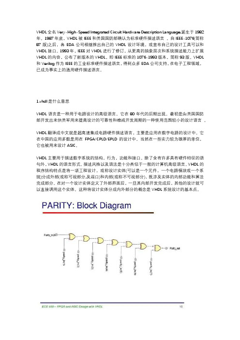
VHDL全名Very-High-Speed Integrated Circuit Hardware Description Language,诞生于1982年。
1987年底,VHDL被IEEE和美国国防部确认为标准硬件描述语言。
自IEEE-1076(简称87版)之后,各EDA公司相继推出自己的VHDL设计环境,或宣布自己的设计工具可以和VHDL接口。
1993年,IEEE对VHDL进行了修订,从更高的抽象层次和系统描述能力上扩展VHDL的内容,公布了新版本的VHDL,即IEEE标准的1076-1993版本,简称93版。
VHDL 和Verilog作为IEEE的工业标准硬件描述语言,得到众多EDA公司支持,在电子工程领域,已成为事实上的通用硬件描述语言。
1.vhdl是什么意思VHDL语言是一种用于电路设计的高级语言。
它在80年代的后期出现。
最初是由美国国防部开发出来供美军用来提高设计的可靠性和缩减开发周期的一种使用范围较小的设计语言。
VHDL翻译成中文就是超高速集成电路硬件描述语言,主要是应用在数字电路的设计中。
它在中国的应用多数是用在FPGA/CPLD/EPLD的设计中。
当然在一些实力较为雄厚的单位,它也被用来设计ASIC。
VHDL主要用于描述数字系统的结构,行为,功能和接口。
除了含有许多具有硬件特征的语句外,VHDL的语言形式、描述风格以及语法是十分类似于一般的计算机高级语言。
VHDL的程序结构特点是将一项工程设计,或称设计实体(可以是一个元件,一个电路模块或一个系统)分成外部(或称可视部分,及端口)和内部(或称不可视部分),既涉及实体的内部功能和算法完成部分。
在对一个设计实体定义了外部界面后,一旦其内部开发完成后,其他的设计就可以直接调用这个实体。
这种将设计实体分成内外部分的概念是VHDL系统设计的基本点。
2.vhdl的作用功能强大、设计灵活VHDL具有功能强大的语言结构,可以用简洁明确的源代码来描述复杂的逻辑控制。
电子信息专业名词

信号是运载信息的工具是消息的载体。
信息的具体表现形式是信号信息是信号包含的内容,没有信息,信号将毫无意义。
AVR单片机是1997年由ATMEL公司研发出的增强型内置Flash的RISC(Reduced Instruction Set CPU) 精简指令集高速8位单片机。
AVR的单片机可以广泛应用于计算机外部设备、工业实时控制、仪器仪表、通讯设备、家用电器等各个领域。
1997年,由Atmel公司挪威设计中心的A先生和V先生,利用Atmel公司的Flash新技术,共同研发出RISC精简指令集高速8位单片机,简称AVRSingle chip microcomputerAltium公司作为EDA领域里的一个领先公司,在原来Protel 99SE的基础上,应用最先进的软件设计方法,率先推出了一款基于Windows2000和Windows XP操作系统的EDA设计软件Protel DXP计算机辅助设计(CAD-Computer Aided Design)指利用计算机及其图形设备帮助设计人员进行设计工作。
PCB(PrintedCircuitBoard),中文名称为印制电路板,又称印刷电路板、印刷线路板,是重要的电子部件,是电子元器件的支撑体,是电子元器件电气连接的提供者。
由于它是采用电子印刷术制作的,故被称为“印刷”电路板。
Dxp 薛晓花电路板单片机 keil Protues 编写程序和仿真 EDA quatuas2 VHDL语言文本输入,图形输入。
数字信号 Matlab 虚拟仪器 Multisim . Labviw 田思全球移动通讯系统Global System of Mobile communication就是众所周知的GSM,是当前应用最为广泛的移动电话标准。
全球超过200个国家和地区超过10亿人正在使用GSM电话。
GSM标准的无处不在使得在移动电话运营商之间签署"漫游协定"后用户的国际漫游变得很平常。
EDA技术概述

1.2 EDA技术实现目标
目标:是完成专用集成电路ASIC的设计和实现
ASIC(ApplicationSpecific Integrated Circuit): 专门为某一应用领域或某一专门用户需要而设计制造的LSI或VLSI 电路。
专用集成电路ASIC是厂家按用户的具体要求(如功能、性能或技术 等),为用户的特定系统定制的集成电路。如彩电RGB三基色处理芯片、
ENTITY counter IS PORT(
clk:IN STD_LOGIC; rs: IN STD_LOGIC; count_out: OUT STD_LOGIC_VECTOR(2 DOWNTO 0)); END counter;
ARCHITECTURE behav OF counter IS
特点: ▼ 20世纪90年代以来, 微电子技术以惊人的速度发展, 其工艺水平达到深亚微米级, 在一个芯片上可集成数百 万乃至上千万只晶体管, 工作速度可达到GHz对EDA系 统提出了更高的要求。 ▼出现了以高级语言描述、 系统仿真和综合技术。
不仅极大地提高了系统的设计效率, 而且使设计人员摆 脱了大量的辅助性及基础性工作, 将精力集中于创造性 的方案与概念的构思上。
一下启/停开关,计时器终止计时;)
主要步骤:
1.根据系统对硬件的要求,详细编制技术规格书,并画出 系统控制流图;
2.根据技术规格书和系统控 制流图,对系统功能进行 细化,合理地划分功能模 块,并画出系统的功能框 图;
3.进行功能模块的细化和电 路设计;
4.各模块电路设计、调试完 成后,将各功能模块的硬 件电路连接起来再进行系 统的调试,最后 完成整个 系统的硬件设计; (特点:整个设计从最 底层开始设计,直到最高 层设计完毕)
EDA的应用及发展趋势

EDA的应用及发展趋势EDA(Electronic Design Automation)即电子设计自动化,是指利用计算机和相关软件工具来辅助电子系统的设计、验证和制造过程。
EDA的应用涉及多个领域,包括芯片设计、电路设计、电子系统级设计等。
首先,EDA在芯片设计方面起到了关键作用。
芯片设计是EDA最早应用的领域之一、芯片设计涉及到复杂的电路、布局和布线,需要大量的计算和优化。
EDA工具在芯片设计中可以帮助设计师进行电路的模拟和优化、物理布局和布线、验证和测试等工作。
通过EDA工具,设计师可以更高效地进行芯片的设计和验证,从而降低设计的时间和成本。
其次,EDA在电路设计方面也起到了重要作用。
电路设计是EDA的另一个重要应用领域。
电路设计包括模拟电路设计和数字电路设计。
模拟电路设计主要涉及到模拟信号的放大、滤波、混频等功能,而数字电路设计则涉及到数字信号的逻辑运算、存储、时序处理等功能。
通过EDA工具,设计师可以进行电路的建模与仿真、逻辑综合与优化、时序分析与约束等工作,加速电路设计的过程,提高设计的质量和可靠性。
此外,EDA在电子系统级设计方面也得到了广泛应用。
电子系统级设计是指对整个电子系统进行设计和优化。
电子系统包括多个芯片、电路和模块,还包括外围器件和接口。
通过EDA工具,设计师可以对电子系统进行架构设计、功能验证、性能分析等工作,以及对系统进行优化和集成。
EDA工具可以帮助设计师减少设计迭代次数,降低系统开发的时间和成本。
未来,EDA的发展趋势有以下几个方向:首先是EDA工具的功能和性能的进一步提升。
随着半导体和集成电路的发展,设计的复杂度和规模不断增加,对EDA工具的功能和性能提出了更高的要求。
未来的EDA工具将更加注重设计的自动化和智能化,提供更加强大和高效的算法和工具,以应对越来越复杂的设计任务。
其次是EDA工具的多学科集成。
未来的EDA工具将会更加注重不同学科领域的融合和协同。
比如,在芯片设计领域,EDA工具将会与材料科学、物理学、光学等领域的工具进行融合,形成更加完整和综合的设计环境。
EDA技术的发展与应用中英文

英文资料及中文翻译Development and application of EDA technologyEDA (Electronics Design Automation) technology is that one kind arising at the historic moment with the development at full speed of the integrated circuit and computer technology is advanced, fast, effective electronic design automation tool. EDA tool regards hardware and software of the computer as the basic workbench, software package in common use of CAD that collect the data base, figure learning, picture theory and topological logic, computational mathematics, optimize theory, etc. multi-disciplinary latest achievement and develops. EDA is a development trend of the electronic designing technique, utilize EDA tool to replace a designer and finish most work in the electronic system design.The implementation method of the digital system has been gone through from discrete component, SSI, MSI evolution at full speed to LSI, VLSI and UVISI too. In order to improve systematic dependability and common ability, the microprocessor and special-purpose integrated circuit (ASIC) have replaced the whole hardware LSI circuit in common use gradually. Can program the logic device (PLD) , especially can be programmed in the making that the logic device(FPLD) is applied to ASIC in a large amount at the scene. In the course of canning program the development of the integrated circuit , the appearance of EDA technology has brought the revolutionary change that the electronic system is designed.With the constant development of the micro-electric technique and computer technology,in the design work of electronic system related to fields, such as communication, national defense, spaceflight, industrial automation, instrument and apparatus, etc,the content of EDA technology is rising at the surprising speed , it has already nowadays become one of the front of the electronic technical development. This text has explained the basic conception and evolution of EDA technology at first, then introduce the essential feature of ESDA from several different respects, Analyse theworkflow on two different levels of EDA technology emphatically finally, namely one grade of designs of circuit and system grade are designed,have introduced a kind of top-down high level electronic design method. 1.PrefaceThe human society has already entered into the highly developed information-based society, the development of the information-intensive society can not do without the progress of the electronic product. The modern electronic product has been presenting the downward trend all the time at but the price while performance improves, complexity increases, and the paces of the model change are quicker and quicker , the main reason which realizes this kind of progress is the development which produces the manufacturing technology and electronic designing technique. The former regards very small process technology as representatives, has already developed the deep sub-micro at present, can integrate several ten million transistors on the chip of several square centimeter ; The latter's core is EDA technology. EDA refers to regarding computer as the workbench, have merged electronic CAD software package in common use that the latest achievement of application electric technology, computer technology, intelligent technology develops into , can carry on the design work of three respects auxiliary mainly: IC designs, electronic circuit design and PCB are designed. Without the support of EDA technology, it is unimaginable that the design that wants to finish above-mentioned very large scale integration is made, conversely, produce manufacturing technology constant to progress and will put forward new request to EDA technology.2.Development of EDA technologyEDA technology is following the development that the computer, integrated circuit, electronic system are designed, have gone through CAD (Computer Assist Design), auxiliary engineering design CAE of computer (Computer Assist Engineering Design) Three developing stages with design automation ESDA of electronic system (Electronic System Design Automation).Review the development course of electronic designing technique in the past 30 years, can divide EDA technology into three stages .The seventies of the 20th century, with hitting the appearance and application of the small- scale integrated circuit, traditional madding maps by hand and designed the printed circuit board and integrated circuit method has been already unable to meet and design the requests of the precision and efficiency, people begin high repeated miscellaneous work connect up and work and edit and replace with CAD tool that analyze such as Butut with two-dimensional level figure products design process. This has produced the first generation of EDA tools. Limited by computer workbench at that time, the design work that can be supported is limited and performance is worse The seventies were CAD stage, people began to carry on the domain editor of IC and PCB overall arrangement to connect up auxiliary with the computer this stage, it is done by hand toreplace, has produced the concept of CAD .The first individual computer platform of work station (Apollo) that appeared in the eighties, has promoted the rapid development of EDA tool. For meet the electronic product in the scale and make the need that have, the second generation of EDA technology taking emulation of the computer and self routing as key technology has appeared. CAE tool with automatic integration capability has replaced some design work of the designer's. Characteristic its to regard software tool as core finish design, analyze, produce, every job of testing etc. of product development through software the. However, EDA tool that the majority proceeds from principle picture still can't meet the request that the complicated electronic system is designed, and the component figure specified is restricting optimization design.The eighties were CAE stage. Compared with CAD, draw the function besides the pure figure , has increased the function of the circuit again and is designed and designed with the structure, and combine the two together through the electric connection network form, in order to realize engineering design, this is a concept of the auxiliary project of the computer. The main function of CAE is: The principle picture is input, logic emulation , the analysis of the circuit, the automatic overall arrangement is connected up, analyze after PCBIn the 1990s, the designer was from using the hardware to be developedand turned from one grade of electronic products of circuit to one grade of electronic product development of system to design the hardware progressively . ESDA tool is designed for the core with the system grade, including the systematic behavior grade describes that comprehensive with the structure grade, with test and prove systematic emulation system divide assign. The appearance of the third generation of EDA technology, the efficiency that the improvement system is designed greatly, dream of making the designer begin to realize that "the concept drive the project ". The designer has got rid of a large amount of auxiliary design work, concentrate energy on creative scheme and concept to conceive , thus improved efficiency of designing greatly, has shortened the research cycle of the products.The 1990s were ESDA stage. Though CAD/CAE technology has made enormous success, has not liberated people completely from the strenuous design work out. In the course of designing entirely, automation and intelligent degree are also not high, various kinds of EDA software interfaces are various, learn and use difficult, and incompatible, influence and design to link up link directly. Because the above is insufficient, people begin to pursue the automation of carrying out whole design process.3.The technology of EDA is formedThe essential feature of modern EDA technology is to adopt the high-level language to describe, have one grade of emulation of system and integration capability. EDA target of technical research the whole course that electron design, have system grade, circuit grade and physics grades of each design of level. The category of technical research of EDA is quite extensive, develops and uses the angle to look from ASIC, include the following sub module : Design introduction sub module, set up and count data base sub module, analyze and prove sub module, comprehensive emulation sub module, overall arrangement connect up sub module etc..EDA adopts the concurrent engineering and " top-down design method " mainly, then designs and starts with from the system, division and structure carrying on the function block-diagram on the top floor are designed, carries on emulation , corrects error first classily in the block-diagram , and describewith the hard wares, such as VHDL, Verilogy-HDL, ABEL etc. that the language describes the high-level systematic behavior, prove in system one grade , optimizes tools and produces the concrete net list in one grade of logical circuits of door synthetically with logic afterwards, it can be a printed circuit board or special-purpose integrated circuit that its corresponding physics is realized grade.The experience of EDA tool is two great stages: Physics tool and logic tool. The actual physics question used for finishing of physics in the design of tool, for instance the overall arrangement of the chip, printed circuit board are connected up etc.. The logic tool is because of the logic of the net-list, cloth, transmit the concepts, such as time sequence etc., described at first that designs introduction in language by the picture editing machine of principle or the hardware, then utilize EDA system to finish being synthesized, course, such as emulation, optimizing etc., the structurization of net-list or VHDL, Virology -HDL turning into the physics tool finally and can be accepted is described. Now common EDA tools have logic, emulation, check analyze by tool, optimize /synthesis tool, etc.At present, PLD has already become the main means that the modern digital system is designed. Traditional programming technology to insert and go on programming at programmable device PLD device, and " can be programmed the appearance of the logic device in the system " (ISP, namely In- System Programmable), has reached limit of the superiority full play of the programming device. ISP technology directly among user design object system or circuit go on the technology of programming to PLD device at the board. Have broken the convention that PLD must be assembled after programming first of using, the programming after can assemble first , can also be programmed repeatedly after becoming the products. ISP allows user's programming " in the system " and revises logic, have provided for user and construct systematic ability and hardware upgrading ability again without revising the systematic hardware to design, make the hardware revised and as convenient like the software revise , systematic dependability improves because of this.4.Development trend of EDA technologyWith the introduction of Intel Company Pentium processor, the listing of FPGA of hundreds of thousands pieces of scale of company, such as Xilinx etc., and extensive chip group and application of the high-speed, high density printed circuit board, EDA technology is in emulation , time sequence analysis, integrated circuit test automatically, high-speed printed circuit board design and expansion of operating platform etc. face the new enormous challenge. These are developments trend in the future of EDA technology of new generation. In the face of the electronic product market that nowadays develops at full speed, the designer needs more practical, swifter EDA tool, use unified integrated design environment, change traditional mentality of designing, concentrate on and get and design and conceive energy, the scheme compares and looks for the respects, such as optimization design etc., develop the of good performance electronic product with first-class quality at fastest speed. Of new generation EDA technology towards powerful simple to learn while being easy, the direction easy to use will be developed. 5.Essential feature of ESDA technologyESDA representatives are nowadays the newest developing direction of electronic designing technique, its essential feature is: The designer divides with the function conceptual design to the whole system according to the " top-down design method ", the key circuit of the system is realized with one or several slices of special-purposes integrated circuit (ASIC), then adopt the hardware to describe that the language (HDL) is finished the systematic behavior grade and designed, produce the final goal device through comprehensive device and adapter finally. The electronic design method known as high level of such a design method, will also do the introduction of deepening in 4.2 in concrete procedure. Now introduce several concepts related to ESDA essential feature.5.1 the“ Top-Down” design method10 years ago, chose the standard integrated circuit to construct out a new system “ Bottom-Up” in basic train of thought that the electron is designed, such a design method build Pyramid like one brick one, it lows with high costs efficiency have to be but also easy to make mistakes.Design the brand-new design method to provide for us a kind of " Top-Down " in high level, designing starting with from the system at first in these kind of design method, division and structure carrying on the function block-diagram on the top floor are designed. Carries on emulation , corrects error first classy in the block-diagram , and describe with the hardware that the language describes the high-level systematic behavior, prove in system one grade. Then by optimizing tools and produce the concrete net-list of pieces of circuit synthetically, it can be a printed circuit board or special-purpose integrated circuit that its corresponding physics is realized grade. Because the main emulation designed and debugging the course to finish on high level, this not merely helps to find the mistake on the structure design in early days, avoid the waste of the design work, and has reduced the work load of logic function emulation , has improved success rate designed.5.2 The designing of ASICThe complexity of the modern electronic product is strengthened day by day, a electronic system may be formed by integrated circuit on a small scale of several tens of thousands of, this has brought volume largely, the consumption is great, problem with bad dependability , the effective method to solve this problem is to adopt ASIC (Application Specific Integrated Circuits) chip to be designed. ASIC can be divided into according to the difference of design methods: Customize ASIC all, half customize ASIC, programmable ASIC (called and can program the logic device too).When design and customize ASIC chip completely, the designer wants to define the geometric figure of all transistors and rule of craft on the chip, design result transfer to IC producer close membrane make and finish finally. The advantage is: The chip can obtain optimum performance, namely area utilization ratio high, fast, low power dissipation . The shortcoming is: Development period is long, costly, only suitable for the product development in enormous quantities.Half customize ASIC domain of chip design method to some extent different, divide into door array design law and standard unit design law, these two kinds of methods are both binding character design methods, its main purpose is simplified and designed, shorten construction period by sacrificing the performance of the chip as the cost. Can program logic chipand above-mentioned difference of covering the membrane ASIC to lie in : The designer can fire out one's own chip in the laboratory after finishing the domain design, needn't have the participation of IC producer, has shortened development period greatly .Can program the logic device since the seventies , has gone through PAL, GAL, CPLD, FPGA several developing stages, among themCPLD/FPGA has belonged to the high density and can program the logic device , the integrated level has already been up to 2 million doors slice at present, it close integrated level high advantage, ASIC of membrane, and can program logic device design and produce convenient characteristic combine together, especially suited to the sample developing short run product development, enable products and list at fastest speed, and when the market expands , it can very easy to transfer to and cover membrane ASIC realize, so develop the risk but greatly reduced .5.3 The hardware describes languagesThe hardware describes that the language (HDL-Hardware Description Language) is a kind of computer language used for designing the electronic system of the hardware, it describe the logic function of the electronic system, circuit structure and connects the form in programming way of software, describe with traditional door grade that the way compares, it is more suitable for the design of the extensive system. Such as one addition device of 32, utilize figure input software need 500 introduction to 1000 door, and utilize VHDL language to only need to write a line of A =B +C, and VHDL language readability is strong, apt to revise and find the mistake. The early hardware described languages, was developed by different EDA manufacturers such as ABEL-HDL, AHDL, not compatible each other, and does not support designing at many levels , translation should be finished artificially among the levels. In order to overcome the above defect, the American Ministry of National Defence put out VHDL (Very High Speed IC Hardware Description Language) language formally in 1985, IEEE adopted VHDL and described the standard of languages (IEEE STD-1076) for the hardware in 1987.VHDL whether one omni-directional hardware describe language,including systematic behavior grade, register transmit grade and logic gate one magnitude of a lot of design levels, support the mixing and describing of three kinds of description forms of the structure, dataflow, behavior, so VHDL nearly covers the functions of describing the language of various kinds of hard wares in the past, whole top-down or the bottom-up circuit design process can be finished with VHDL. In addition, VHDL also has the following advantages :The wide range of VHDL describes the core that ability makes it become high level and is designed, has brought the designer's focus of work up to the realization and debugging of the systematic function, less energy is used in physics to realize to only need flowersVHDL can describe with the succinct and clear code that controls the logic design complicatedly, flexible and convenient, but also easy to design the exchange, save of the result and put in an position.The design of VHDL does not depend on the specific device , has facilitated the conversion of the craft .VHDL is a standard language, support for numerous EDA manufacturers , so the transplanting is good.5.4 Systematic frame structureEDA systematic frame structure (Framework) is a set of norms of disposing and use EDA software package, present main EDA system all set up frame structure, for instance Design Framework of Cadence Company, Falcon Framework of Mentor Company etc., these frame structure is all in accordance with the unified technical standard that international CFI organization (CAD Framework Initiative) make . Framework can carry on optimization grouping of the tool software from different EDA manufacturers , integrates it under a unified environment of easy management, and still support and realize the transmission and sharing of information in the course of whole product development between the tasks, between the designers, this is a realization foundation of a co-current engineering and Top-Down design method.6. ConclusionEDA technology whether electron design a revolution of field, atdeveloping stage of high speed at present, there are new EDA tools every year to come out, the application level of EDA technology of our country lags behind the developed country for a long time, so, the masses of electronic engineering personnel should master this advanced technology as soon as possible , this improve design need of efficiency is of our country electronics industry survive at world market even more, strive and need that develop unexpectedly.EDA技术的发展与应用EDA(Electronics Design Automation电子设计自动化)技术是随着集成电路和计算机技术的飞速发展应运而生的一种高级、快速、有效的电子设计自动化工具。
EDA外文翻译

Electronic Design AutomationEDA (Electronic Design Automation, Electronic Design Automation) technology is the modern field of electrical engineering a new technology, which provides computer-based information technology and circuit design methods. EDA technology development and application of greatly promoted the development of the electronics industry. With the development of EDA technology, hardware design of electronic circuits can rely on almost all computers to accomplish, thus greatly shortening the cycle of hardware electronic circuit design, enabling manufacturers to quickly develop a variety of small quantities of products to meet the market demand. EDA technology, the basic idea is the help of computers, the EDA software platform to complete electronic circuit design, simulation and PCB design of the entire process. For more complex circuits, if necessary, can be used to implement programmable logic devices. EDA technology not only on the Electronic Course and analysis of simulation experiments to address the variety of laboratory components, specifications and quantity restrictions are not sufficient to avoid damage to the students in the lab components and devices to stimulate interest in learning, to develop their analysis, electronic product design and development ability, but also e-workers to design, develop a powerful tool for electronic products. Thinking of EDA technology education and industry promotion is a technology hot spot in today's world, EDA technology is indispensable in the modern electronics industry to a technology. EDA technology has a broad meaning, but also a progressive development of the field has a strong vitality. Today's EDA technology has reached a "system on a chip" (SOC, System On Chip) stage. Developers can use the powerful EDA design software, the use of IP (Intellectual Property) IP core, coupled with his innovative thinking, and build their own custom chips, which have their own IP rights to design specific integrated circuit (ASIC, Application Specific IC .) EDA technology in the popularity of teaching, practical applications based on programmable device technology, which includes four basic conditions:①large-scale programmable devices, it is the use of EDA techniques carrier electronic system design;②hardware description language It is the use of EDA technologies for electronic system design, the main means of expression;③software development tools, it is the use of EDA technologies for intelligent electronic system design automation design tools.④experimental development system, which is the use of EDA technology for electronic systems Download tools and hardware design verification tools.Programmable Logic Control (CPLD / FPGA)In our design, we was selected CPLD / FPGA, as compared with the traditional MCU has many advantages, mainly in the following areas:①advanced programming very easy. CPLD / FPGA products, part of the daisy chain in-system programming mode. This advanced method of programming has become the world's development trend of various types of programmable devices. Because it obviates the expensive and inconvenient operation dedicated programmer, just need to download a very simple programming circuit and a PC, printer communication cable on the line. It is not programmed pressure, the TTL level line can be programmed at any time, and the so-called multi-chip daisy chain serial programming. Its programming up to 1 million times, such as Lattice's isles and AMD's MACH family. In addition, programming can easily achieve infrared, ultrasonic or radio programming programmer, or through the telephone line remote online programming. These features are in communication devices and military special purpose devices.② high speed. CPLD / FPGA clock delay of up to ns level, combined with the parallel work,in the ultra high-speed real-time monitoring and control applications and has a very broad application prospects. If you use the FLEX10K50 ALTERA development network image through USB interface, real-time encryption / decryption ASIC system, carried out in FLEX10K50 up to 56-bit parallel binary arithmetic, each encryption / decryption cycle of only a few μs, and the MCU takes nearly 1 minute . Another example is in the mold manufacturing EDM processing, motor control, the effective operation of the processing parts from only a few μs, which is required for the control of sensitive and high-speed circuit feeding service, not a short circuit or arcing is less than the breakdown . Obviously, this work, MCU is difficult to directly participate. If direct feeding by ispLSI1032 service control, feeding on the closed-loop motor speed service, the use of sampling ispLSI direct control of the AD1674, 8-bit accuracy using a maximum speed of 8μs / each, in order to achieve a good closed-loop speed control of synchronous and .③ high reliability. In high reliability applications, MCU's shortcomings as a CPLD / FPGA application left a lot of useless. Although the function of this group developed the device is achieved through the EDA software. But the physical mechanism like a 74LS164 as purely a hardware circuit is very reliable. Through the rational design of most applications, no need to consider the complex reset and initialization. Design using a simple statement just idle initial entry into the same, we can effectively prevent any possible "death" phenomenon. Because it is working in parallel, it can be used as either input pin interrupt monitoring is similar to pin MCU, and the reaction rate is only satisfied wonderful class. CPLD / FPGA, high reliability is also reflected in almost the entire system can be downloaded on the same chip, thus greatly reducing the volume, easy to manage and shielding.④powerful, applications are broad. Currently, CPLD / FPGA to select a large range, according to different applications use different capacity chips, such as Lattice's ispLSI and AMD's MACH, the smallest chip for the 1000 equivalent logic gates, the largest of several one hundred thousand . ALTERA and XILINX gate introduced millions of CPLD / FPGA can achieve almost any form of digital circuits or digital systems design. With the wide application of such devices and the cost dropped significantly, and the market rate increase, CPLD / FPGA in the system rate is almost equal to the direct application of ASIC development.⑤ easy to use, develop convenient. The design of SCM experts in application system is very simple. However, for beginners, such as the CPU's work, many of the usage of special registers, interrupt concepts, etc., really is not an easy task. In contrast, CPLD / FPGA application does not require too much preparation to learn the knowledge, as long as a little bit of design of digital circuits and computer software basics, you can in the short term to handle basic design and development skills. And in turn, to learn to use SCM, it appeared hundreds of times more. This is undoubtedly high for us to provide a shortcut to learning, standing on the shoulders of giants, of course faster to be successful. It can be predicted, the study of EDA technology boom and the CPLD / FPGA application boom never inferior to boom over the past 10 years, single chip.⑥ short development cycle. EDA software features as the corresponding sound and powerful, convenient and real-time simulation capabilities, and intuitive image of the development process, and the hardware factors involved very little, it can be very complicated in a very short time the system design, which is the product to market quickly the most valuable features. Some EDA experts predict, the future of large-scale systems of CPLD / FPGA design is just all kinds of logic and then apply the IP core (CORE) of the assembly, the design cycle, only hour. TI company that eighty percent of an ASIC IP core features available such as ready-made logic synthesis.1.Development of language VHDLVHDL (Very High Speed Integrated Circuit Hardware Description Language) is a very highspeed integrated circuit hardware description language, it can describe the function of the hardware circuitry, signal connectivity and the time between languages. It can be more effective than the circuit diagram to express the characteristics of the hardware circuit. Using the VHDL language, you can proceed to the general requirements of the system, since the detailed content will be designed to come down to earth, and finally to complete the overall design of the system hardware. IEEE VHDL language has been the industry standard as a design to facilitate reuse and sharing the results. At present, it can not be applied analog circuit design, but has been put into research. VHDL program structure, including: entity (Entity), structure (Architecture), configure (Configuration), Package Collection (Package) and the Library (Library). Among them, the entity is the basic unit of a VHDL program, by entity and the structure of two parts: the physical design system that is used to describe the external interface signal; structure used to describe the behavior of the system, the system processes or system data structure form. Configuration select the required language from the library system design unit to form different versions of different specifications, so that the function is designed to change the system. Collection of records of the design module package to share the data types, constants, subroutines and so on. Database used to store the compiled entities, the body structure, including the collection and configuration: one is the development of engineering software user, the other is the manufacturer's database.VHDL, the main features are:①powerful, high flexibility: VHDL language is a powerful language structure, clear and concise code can be used to design complex control logic. VHDL language also supports hierarchical design, support design databases and build reusable components. Currently, VHDL language has become a design, simulation, synthesis of standard hardware description language.② Device independence: VHDL language allows designers to generate a design do not need to first select a specific device. For the same design description, you can use a variety of different device structures to achieve its function. So the design description stage, able to focus on design ideas. When the design, simulation, after the adoption of a specific device specified integrated, adapter can be.③ Portability: VHDL language is a standard language, so the use of VHDL design can be carried out by different EDA tool support. Transplanted from one to another simulation tools simulation tools, synthesis tools from a port to another integrated tool, from a working platform into another working platform. EDA tools used in a technical skills, in other tools can also be used.④top-down design methods: the traditional design approach is bottom-up design or flat design. Bottom-up design methodology is to start the bottom of the module design, the gradual formation of the functional modules of complex circuits. Advantage of this design is obvious because it is a hierarchical circuit design, the general circuit sub-module are in accordance with the structure or function of division, so the circuit level clear, clear structure, easy people to develop, while the design archive file is easy, easy communication. Bottom-up design is also very obvious shortcomings, the overall design concept is often not leaving because the cost of months of low-level design in vain. Flat design is a module containing only the circuit, the circuit design is straightforward and, with no division structure and function, it is not hierarchical circuit design. Advantages of small circuit design can save time and effort, but with the increasing complexity of the circuit, this design highlights the shortcomings of the abnormal changes. Top-down design approach is to design top-level circuit description (top model), and then the top-level simulation using EDA software, if the top-level design of the simulation results meet the requirements, you can continue to lower the top-level module by the division level and simulation, design of such alevel will eventually complete the entire circuit. Top-down design method compared with the first two are obvious advantages.⑤rich data types: as a hardware description language VHDL data types are very rich language, in addition to VHDL language itself dozens of predefined data types, in the VHDL language programming also can be user-defined data types. Std_logic data types in particular the use of VHDL language can make the most realistic complex signals in analog circuits.⑥modeling convenience: the VHDL language can be integrated in the statement and the statement are available for simulation, behavior description ability, therefore particularly suitable for signal modeling language VHDL. The current VHDL synthesizer to complex arithmetic comprehensive descriptions (such as: Quartus Ⅱ 2.0 and above versions of std_logic_vector type of data can add, subtract, multiply, divide), so the circuit modeling for complex simulation of VHDL language, whether or comprehensive description of the language are very appropriate.⑦ rich runtime and packages: The current package supports VHDL, very rich, mostly in the form of libraries stored in a specific directory, the user can at any time. Such as the IEEE library collection std_logic_1164, std_logic_arith, std_logic_unsigned other package. In the CPLD / FPGA synthesis, EDA software vendors can also use the various libraries and provide package. VHDL language and the user using a variety of results can be stored in a library, in the design of the follow-up can continue to use.⑧ VHDL language is a modeling hardware description language, so with ordinary computer languages are very different, common computer language is the CPU clock according to the beat, after an instruction to perform the next instruction, so instruction is a sequential, that is the order of execution, and execution of each instruction takes a specific time. VHDL language to describe the results with the corresponding hardware circuit, which follows the characteristics of hardware, there is no order of execution of the statement is executed concurrently; and statements that do not like ordinary software, take some time each instruction, just follow their own hardware delay.2. Development Environment MAX + PLUSⅡ/ QUARTERⅡAltera Corporation is the world's three major CPLD / FPGA manufacturers of the devices it can achieve the highest performance and integration, not only because of the use of advanced technology and new logic structure, but also because it provides a modern design tools MAX + PLUSⅡprogrammable logic development software, the software is launched the third generation of Altera PLD development system. Nothing to do with the structure provides a design environment for Altera CPLD designers to easily design entry, quick processing, and device programming. MAX + PLUSⅡprovides a comprehensive logic design capabilities, including circuit diagrams, text and waveform design entry and compilation, logic synthesis, simulation and timing analysis, and device programming, and many other features. Especially in the schematic so, MAX + PLUSⅡis considered the most easy to use, the most friendly man-machine interface PLD development software. MAX + PLUSⅡcan develop anything other than the addition APEX20K CPLD / FPGA.MAX + PLUSⅡdevelopment system has many outstanding features:① open interface.②design and construction related: MAX + PLUSⅡsupport Altera's Classic, ACEX 1K, MAX 3000, MAX 5000, MAX 7000, MAX 9000, FLEX 6000, FLEX 8000 and FLEX 10K series of programmable logic devices, gate count is 600 ~ 250 000 doors, offers the industry really has nothing to do with the structure of programmable logic design environment. MAX + PLUSⅡcompiler also provides a powerful logic synthesis and optimization to reduce the burden on the user's design.③ can be run on multiple platforms: MAX + PLUSⅡsoftware PC-based WindowsNT 4.0, Windows 98, Win dows 2000 operating systems, but also in Sun SPARCstations, HP 9000 Series 700/800, IBM RISC System/6000 such as run on workstations.④ fully integrated: MAX + PLUSⅡsoftware design input, processing, calibration functions are fully integrated within the programmable logic development tools, which can be debugged more quickly and shorten the development cycle.⑤modular tools: designers can input from a variety of design, editing, calibration and programming tools to choose the device to form a user-style development environment, when necessary, to retain on the basis of the original features to add new features. The MAX + PLUSⅡSeries supports a variety of devices, designers need to learn new development tools for the development of new device structures.⑥mail-description language (HDL): MAX + PLUSⅡsoftware supports a variety of HDL design entry, including the standard VHDL, Verilog HDL and Altera's own developed hardware description language AHDL.⑦MegaCore Function: MegaCore are pre-validated for the realization of complex system-level functions provided by the HDL netlist file. It ACEX 1K, MAX 7000, MAX 9000, FLEX 6000, FLEX 8000 and FLEX 10K devices provide the most optimal design. Users can purchase them from the Altera MegaCore, using them can reduce the design task, designers can make more time and energy to improve the design and final product up.⑧OpenCore Features: MAX + PLUSⅡsoftware with open characteristics of the kernel, OpenCore come to buy products for designers design their own assessment.At the same time, MAX + PLUSⅡthere are many other design entry methods, including:① graphic design input: MAX + PLUSⅡgraphic design input than other software easier to use features, because the MAX + PLUSⅡprovides a rich library unit for the designer calls, especially in the MAX2LIB in the provision of the mf library includes almost all 74 series of devices, in the prim library provides all of the separate digital circuit devices. So long as a digital circuit knowledge, almost no learning can take advantage of excess MAX + PLUSⅡfor CPLD / FPGA design. MAX + PLUSⅡalso includes a variety of special logic macros (Macro-Function) and the parameters of the trillion of new features (Mega-Function) module. Full use of these modules are designed to greatly reduce the workload of designers to shorten design cycles and multiply.② Enter the text editor: MAX + PLUSⅡtext input language and compiler system supports AHDL, VHDL language, VERILOG language of the three input methods.③wave input: If you know the input, output waveform, the waveform input can also be used.④hybrid approach: MAX + PLUSⅡdesign and development environment for graphical design entry, text editing input, waveform editing input hybrid editing. To do: in graphics editing, wave form editing module by editing the text include "module name. Inc" or the use of Function (... ..) Return (....) Way call. Similarly, the text editing module input form can also be called when the graphics editor, AHDL compiler results can be used in the VHDL language, VHDL compiler of the results can also be entered in the AHDL language or graphic to use. This flexible input methods, to design the user has brought great convenience.Altera's QuartusⅡis a comprehensive PLD development software to support the schematic, VHDL, Verilog HDL, and AHDL (Altera Hardware Description Language) and other design input forms, embedded devices, and integrated its own simulator, you can complete the design input to complete the hardware configuration of the PLD design process.QuartusⅡin the XP, Linux and Unix on the use, in addition to using the Tcl script to complete the design process, to provide a complete graphical user interface design. With running speed, unified interface, feature set, easy to use and so on.Altera's QuartusⅡsupport IP core, including the LPM / MegaFunction macro function module library, allowing users to take full advantage of sophisticated modules, simplifying the design complexity and speed up the design speed. Good for third-party EDA tool support also allows the user to the various stages in the design process using the familiar third-party EDA tools.In addition, QuartusⅡand DSP Builder tools and by Matlab / Simulink combination, you can easily achieve a variety of DSP applications; support Altera's programmable system chip (SOPC) development, set system-level design, embedded software development, programmable logic design in one, is a comprehensive development platform.MaxPLUSⅡgeneration as Altera's PLD design software, due to its excellent ease of use has been widely used. Altera has now stopped MaxPLUSⅡupdate support, QuartusⅡnot only support the device type as compared to the rich and the graphical interface changes. Altera QuartusⅡincluded in many such SignalTapⅡ, Chip Editor and RTL Viewer design aids, integrated SOPC and HardCopy design process, and inherit MaxPLUSⅡfriendly graphical interface and easy to use.MaxPLUSⅡgeneration as Altera's PLD design software, due to its excellent ease of use has been widely used. Altera has now stopped MaxPLUSⅡupdate support, QuartusⅡnot only support the device type as compared to the rich and the graphical interface changes. Altera QuartusⅡincluded in many such SignalTapⅡ, Chip Editor and RTL Viewer design aids, integrated SOPC and HardCopy design process, and inherit MaxPLUSⅡfriendly graphical interface and easy to use.Altera QuartusⅡas a programmable logic design environment, due to its strong design capabilities and intuitive interface, more and more digital systems designers welcome.Altera's QuartusⅡis the fourth generation of programmable logic PLD software development platform. The platform supports a working group under the design requirements, including support for Internet-based collaborative design. Quartus platform and Cadence, ExemplarLogic, MentorGraphics, Synopsys and Synplicity EDA vendors and other development tools are compatible. LogicLock improve the software module design features, added FastFit compiler options, and promote the network editing performance, and improved debugging capabilities. MAX7000/MAX3000 devices and other items to support the product.附录B:中文翻译可编程逻辑控件(CPLD/FPGA)在我们的设计中我们之所以选用CPLD/FPGA,因为它与传统的MCU相比有着许多优点,主要有以下几个方面:①编程方式简便先进。
EDA技术与VHDL实用教程
EDA技术与VHDL实用教程
EDA与传统电子设计方法的比较
FPGA和DSP芯片实现FIR滤波器的速度对比
8位FIR滤 FPGA的处理速度 达到相当速度所需DSP芯片的指令执行速度
波器阶数
单位: MSPS
单位:MIPS
8
104
832
16
24
101
103
1616
2472
32
EDA技术与VHDL实用教程
EDA技术与VHDL实用教程
11
VHDL语言是一种高级描述语言,适用于 电路高级建模,综合的效率和效果较好。
Verilog-HDL语言是一种低级的描述语言, 适用于描述门级电路,容易控制电路资源, 但其对系统的描述能力不如VHDL语言。
EDA技术与VHDL实用教程
12
(二)可编程逻辑器件 可编程逻辑器件(简称PLD)是一种由用户 编程来实现某种逻辑功能的新型逻辑器件。
Expert LEVER
Actel
EDA技术与VHDL实用教程
IspLSI、pLSI、 MACH等
SX系列、MX系列
逻辑图、VHDL文本等 逻辑图、VHDL文本等
16
Actel Designer
EDA与传统电子设计方法的比较
手工设计方法的缺点是: 1)复杂电路的设计、调试十分 困难。 2)如果某一过程存在错误,查 找和修改十分不便。 3)设计过程中产生大量文档, 不易管理。 4)对于集成电路设计而言,设 计实现过程与具体生产工艺直 接相关,因此可移植性差。 5)只有在设计出样机或生产出 芯片后才能进行实测。 EDA技术有很大不同: 1)采用硬件描述语言作为设计输入。 2)库(Library)的引入。 3)设计文档的管理。 4)强大的系统建模、电路仿真功能。 5)具有自主知识产权。 6)开发技术的标准化、规范化以及IP 核的可利用性。 7)适用于高效率大规模系统设计的自 顶向下设计方案。 8)全方位地利用计算机自动设计、仿 真和测试技术。 9)对设计者的硬件知识和硬件经验要 求低。 10)高速性能好。 11)纯硬件系统的高可靠性。
哪些专业学eda技术及应用

哪些专业学eda技术及应用EDA(Electronic Design Automation)是电子设计自动化的缩写,是指利用计算机软件工具来辅助设计电子系统的过程。
EDA技术及应用广泛应用于集成电路的设计和验证、通信系统的设计和优化、嵌入式系统设计、数字信号处理等领域。
下面是一些学EDA技术及应用的专业:1. 电子信息工程专业:电子信息工程专业是培养具有电子技术、通信技术等方面的综合知识和能力的高级工程技术人才的专业。
在该专业中,学生将学习到EDA的基础知识和技术,并通过课程和实践培养对EDA工具和软件的熟练使用能力。
2. 电子科学与技术专业:电子科学与技术专业是培养从事电子科学与技术研究、开发和管理等方面工作的高素质应用型和技术型人才的专业。
在该专业中,学生将学习到EDA的原理和方法,通过实验和项目实践掌握EDA软件工具的使用和应用。
3. 计算机科学与技术专业:计算机科学与技术专业是培养掌握计算机科学与技术基础理论和基本知识,具备计算机软硬件系统设计、开发、应用和管理等工作能力的高级人才的专业。
在该专业中,学生将学习到EDA的相关算法和方法,并通过实验和项目实践应用于电子系统设计和电路的优化等领域。
4. 微电子学专业:微电子学专业是培养能够从事微电子学科领域研究和技术开发、电子工程中微电子器件和集成电路设计与制造研究和工程应用的高层次复合型人才的专业。
在该专业中,学生将学习到EDA技术在集成电路设计和验证中的应用,以及面向芯片设计的EDA软件工具的使用。
5. 自动化专业:自动化专业是培养德、智、体全面发展,掌握自动化原理和技术的高级工程技术人才的专业。
在该专业中,学生将学习到EDA技术在自动化控制系统设计和优化中的应用,以及EDA软件工具的使用和仿真实验。
6. 通信工程专业:通信工程专业是培养掌握通信技术与通信系统设计、通信网络设计与应用、通信系统与网络的管理与维护、新型通信技术与应用开发等基础理论和专业知识的高级应用型专门人才的学科。
EDA

EDA的发展史及发展趋势EDA是电子设计自动化(Electronic Design Automation)的缩写,在20世纪60年代中期从计算机辅助设计(CAD)、计算机辅助制造(CAM)、计算机辅助测试(CA T)和计算机辅助工程(CAE)的概念发展而来的。
EDA技术就是以计算机为工具,设计者在EDA软件平台上,用硬件描述语言VHDL完成设计文件,然后由计算机自动地完成逻辑编译、化简、分割、综合、优化、布局、布线和仿真,直至对于特定目标芯片的适配编译、逻辑映射和编程下载等工作。
EDA技术的出现,极大地提高了电路设计的效率和可操作性,减轻了设计者的劳动强度。
利用EDA工具,电子设计师可以从概念、算法、协议等开始设计电子系统,大量工作可以通过计算机完成,并可以将电子产品从电路设计、性能分析到设计出IC版图或PCB版图的整个过程的计算机上自动处理完成。
现在对EDA的概念或范畴用得很宽。
包括在机械、电子、通信、航空航天、化工、矿产、生物、医学、军事等各个领域,都有EDA的应用。
目前EDA技术已在各大公司、企事业单位和科研教学部门广泛使用。
例如在飞机制造过程中,从设计、性能测试及特性分析直到飞行模拟,都可能涉及到EDA技术。
EDA技术的概念EDA技术是指以计算机为工作平台,融合了应用电子技术、计算机技术、信息处理及智能化技术的最新成果,进行电子产品的自动设计。
利用EDA工具,电子设计师可以从概念、算法、协议等开始设计电子系统,大量工作可以通过计算机完成,并可以将电子产品从电路设计、性能分析到设计出IC版图或PCB版图的整个过程的计算机上自动处理完成。
回顾近30年电子设计技术的发展历程,可将EDA技术分为三个阶段。
七十年代为CAD阶段,人们开始用计算机辅助进行IC版图编辑、PCB布局布线,取代了手工操作,产生了计算机辅助设计的概念。
八十年代为CAE阶段,与CAD相比,除了纯粹的图形绘制功能外,又增加了电路功能设计和结构设计,并且通过电气连接网络表将两者结合在一起,实现了工程设计,这就是计算机辅助工程的概念。
- 1、下载文档前请自行甄别文档内容的完整性,平台不提供额外的编辑、内容补充、找答案等附加服务。
- 2、"仅部分预览"的文档,不可在线预览部分如存在完整性等问题,可反馈申请退款(可完整预览的文档不适用该条件!)。
- 3、如文档侵犯您的权益,请联系客服反馈,我们会尽快为您处理(人工客服工作时间:9:00-18:30)。
EDA的发展及VHDL的应用90's in 20 centuries, international last electronics and calculator technique more the forerunner's nation, has been being actively investigating a new design method of the electronics electric circuit, and carried on an exhaustive change in the aspects of designing a method, tool wait, obtain huge success.At the design realm of the electronics technique, the application of programmable logic spare part(like CPLD, FPGA), have already got extensive universality, these spare parts brought tremendous vivid for the design of numerical system.These spare parts can pass a software plait a distance but as to it's hardware structure and work the way carry on heavy Gou and make thus the design of hardware can like software design so convenient fast.The all these biggest changed a traditional numerical method, design process of the system design and design idea and promoted the EDA technical quick development.The EDA is an electronics design automation(the Automation of the Electronic Design) of abbreviation, design(CAD) from the calculator assistance at the beginning of 90's in 20 centuries, calculator assistance manufacturing(CAM), calculator assistance test(CAT) and calculator lend support to the concept of engineering(CAE) a development since then.The EDA technique is to take calculator as tool, design at EDA software terrace up, use the hardware description language HDL completion a design a document, then is of oneself completed logic to edit and translate, turn Chien, partitioned by the calculator, comprehensive, excellent turn, set up, cloth line with imitate really, until for particular target chip of proper go together with to edit and translate, the logic reflect to shoot with plait distance download etc. work.The EDA technical emergence, biggest raised efficiency and maneuverability of electric circuit design, eased to design of labor strength.These spare parts can pass a software plait a distance but as to it's hardware structure and work the way carry on heavy Gou and make thus the design of hardware can like software design so convenient fast.The all these biggest changed a traditional numerical method, design process of the system design and design idea and promoted the EDA technical quick development.Make use of EDA tool, the electronics designer can start design electronics system from the concept, calculate way, agreement...etc., a great deal of work can pass calculator completion, and can design the electronics product is from the electric circuit, the function analyze compute of the whole process of design an IC landscape or PCB landscape on board auto processing completion.Use to the EDA concept or category very breadth now.Include in each realm of the machine, electronics, correspondence, aviation aerospace, chemical engineering, mineral, living creature, medical science, military...etc., all there is EDA application.The EDA technique has already extensively used in each archduke department, the Qi business unit and research teaching section currently.For example in the airplane the manufacturing the process, from design, performance test and characteristic analytical until fly emulation, may involve an EDA technique.The EDA technique that this text point mainly to the design, PCB design of the electronics electric circuit and IC design. The EDA design can is divided into system class, electric circuit class and physics to carry out class. The EDA in common use software:The EDA tool pile up one after another and get into an our country currently and have the EDA software of extensive influence to have:MultiSIM 7(the latest edition of original EWB), PSPICE, OrCAD, PCAD, Protel, Viewlogic, Mentor, Graphics, Synopsys, LSIIogic, Cadence, MicroSim, ISE, modelsim etc..These tools all have stronger function, generally can used for a few aspects, for example a lot of softwares all can carry on an electric circuit design with imitate really, together entering can also carry on PCB to automatically set up cloth line, can output various net form a document with the third square software connect.The VHDL English full name be the HardwareDescription Language of the Integrated Circuit of the Very-High-Speed, birth in 1982.At the end of 1987, the VHDL is confirm by IEEE and American Ministry ofNational Defense to describe language for the standard hardware.Announced VHDL standard edition from the IEEE, IEEE-1076(call 87 versions) after, the each EDA company released own VHDL design environment one after another, or declared that the own design tool can connect with VHDL.Henceforth the VHDL designed realm to get to extensively accept in the electronics, and gradually replaced an originally not- standard hardware description language.In 1993, the IEEE carried on to revise to the VHDL, describe ability to up expand a VHDL contents from higher abstract layer and the system, announced the VHDL of new edition, namely IEEE standard of 1076-1993 editions, .(call 93 versions)Now, VHDL and Verilog are the industrial standard hardware description of the IEEEs language, again arrive support of numerous EDA companies, at electronics engineering realm, have become in general use hardware to describe language in fact.There is expert think, in the new century in, the VHDL will start to undertake a greatly part of numerical system design mission at the Verilog language. The VHDL language is a kind of deluxe language which useds for an electric circuit design.It expects to appear after the 80's of.BE at the beginning come out by American Ministry of National Defense development to provide the American solider with the credibility which uses to raise a design with cut 1 kind of development period to use the scope smaller design language.All of VHDL Englishes write BE:The Descriptiong Language of the VHSIC(the Speed Integrated of the Very High Circuit) Hardware.Translating into Chinese is soon extremely high the description language of the integrated circuit hardware.So it of the application mainly is an application in the design of numerical electric circuit.Currently, it is in the application most in China is the design which uses in the FPGA/CPLD/EPLD.Certainly in some units with stronger real strenght, it is also use to design ASIC.The VHDL mainly useds for the structure, behavior which describes numerical system, function with connect.In addition to implying many languages sentence which have a hardware characteristic, VHDL languages forms and description style and sentence construction are very similar at general calculator deluxe language.VHDL procedure structure characteristics is an engineering design, or call that the design entity(can be a component, an electric circuit mold piece or a system) is divided into exterior(or call but part, and port) with inner part(or call to can't see part), since involve internal function and calculate way of entity to complete part of.At to 1 designed entity to define exterior interface after, once it internal development completion after, other designs can directly adjust to use this entity.This kind of will design entity to be divided into a little bit basic VHDL system that is a VHDL system inside the concept of outside part design design of a little bit basic and other hardware describe the language compare and the VHDL has a following characteristics: The function is strong and the design be vivid.The VHDL has the function strong language structure, can describe a complicated logic control with the simple and direct and explicit source code.It has a multi-layer design description function, in multiple layers thin turn, finally directly born electric circuit class description.The VHDL supports synchronous electric circuit, difference's tread electric circuit with random the design of electric circuit, this be the other hardware description although the language can't compare to.The VHDL still supports various design method, since support from the bottom upward design, support again from the design of crest declivity;Since the support mold piece turns a design, support layer's turn a design again. Support extensively and be easy to a modification.Because the VHDL has already become IEEE standard the norm of hardware description language, most EDA tools almost support VHDL currently, this is VHDL of further expansion with extensively applied lay foundation.In the design process of the hardware electric circuit, the main design document is the source code which writes with the VHDL, the VHDL easily reads with the structure turn, so be easy to a modification design.The strong system hardware describes ability.The VHDL has a multi-layer design description function, since can describe system class electric circuit, can describe door class electric circuit again.And description since can adopt a behavior description, deposit a machine to deliver description or structure description, can also adopt thehybrid description of threes mixture.Moreover, VHDL support is inertial to delay and deliver to delay, can also accurately build up hardware electric circuit model.VHDL support prepare definite of with from definition of data type, bring hardware description a bigger freedom degree, make design the personnel can expediently establish the system model of high time. The independence is at the design of spare part, have nothing to do with the craft.Don't need to consider a choice completion the spare part of design first while designing a personnel to carry on a design with the VHDL, can concentrate energy to carry on design of excellent turn.When the design description complete after, can carry out its function with various different spare part structure. Very strong transplantation ability.The VHDL is a kind of hardware description for standardize language, the same of design description can be support by the different tool and make to design to describe of the transplantation make possible.Be easy to a share and reply to use.The VHDL adoption can build up various mold piece that can again make use of according to the design method of database(Library).These canned in advance design or use to design a medium backup mold a piece before and depositted these to the database in, can be in laterly of the design carry on replying to use, can make the design result be design the personnel's to carry on exchanges and share, decrease hardware electric circuit design.(1)compared with other hardware description languages, the VHDL have stronger behavior description ability, come to a decision him to become a system design realm the best hardware a description language thus.The strong behavior description ability is to avert from concrete spare part structure and describe and design important assurance of large-scale electronics system from the logic behavior.(2)the VHDL be abundant of imitate true language sentence and database function, make in any big system of the design can inspect a function possibility of design the system in early days, can carry on imitating true emulation to the design at any time.(3)the ability and procedure structure of the behavior description with lexical VHDL come to a decision the decomposition that he has to support a large-scale design with have already have design of again make use of function.Meet the market demanding large-scale system efficiently, the completion of the high speed has to include many people the several generation hair set even together and abreast works and then can carry out.(4)for use the design of an assurance of VHDL completion, can make use of EDA tool to carry on logic comprehensive with excellent turn, and auto of the VHDL describe the design change into the door class net form.(5)the description of VHDL to design have opposite and independent, the design can not understand the structure of hardware and need not manage the target spare part that the end design carry out, either is what, but carry on an independent design.Founded in 1981, this year has entered the Mentor of 25 years, is the oldest in the three major electronic design automation (EDA) vendors, and turnover ahead of a competitor four times, in addition to Mentor system design tools, market share, ranking first in the world, especially in the PCB layout, Mentor strengths which also ranked first in the world, its turnover is a full 1.5 times the second supplier. To assist customers in China "audiovisual" application-specific markets, "Technical Support" Mentor the largest part of human input (in the past each year is almost more than three times the rate of growth) in order to strengthen the ability of the Physical the Design and Functional Architecture ; and for the continued development of database management tool is also spared no effort in shipment volume growth of around 20% in the past five years, 15% of the revenue progress, is the fastest-growing EDA manufacturers.20世纪90年代,国际上电子和计算机技术较先进的国家,一直在积极探索新的电子电路设计方法,并在设计方法、工具等方面进行了彻底的变革,取得了巨大成功。