两通道单刀双掷模拟开关
单刀双掷开关的连接方法

单刀双掷开关的连接方法单刀双掷开关是一种常见的电气开关设备,广泛应用于各种电路中。
其独特的连接方法使得电路的开关和切换更加方便和灵活。
本文将介绍单刀双掷开关的连接方法以及其在电路中的应用。
一、单刀双掷开关的基本结构单刀双掷开关由一个可旋转的开关轴和三个接线端口组成。
开关轴上有一个可旋转的开关杆,可以使电流在两个不同的接线端口之间切换。
二、单刀双掷开关的连接方法单刀双掷开关的连接方法有多种,下面将介绍两种常见的连接方法。
1. 并联连接方法并联连接方法是指将两个或多个单刀双掷开关的接线端口通过导线连接在一起的方法。
这种连接方法可以实现多个开关同时切换,从而实现电路的复杂控制。
在并联连接方法中,各个开关的接线端口可以根据实际需求选择不同的连接方式,如串联、并联或混合连接。
2. 串联连接方法串联连接方法是指将两个单刀双掷开关的接线端口依次连接在一起的方法。
这种连接方法可以实现一个开关的切换控制。
在串联连接方法中,第一个开关的一个接线端口与电源相连,另一个接线端口连接到第二个开关的一个接线端口,第二个开关的另一个接线端口则连接到负载。
通过旋转第一个开关的开关杆,可以实现电流在负载和电源之间的切换。
三、单刀双掷开关的应用单刀双掷开关广泛应用于各种电路中,具有以下几个方面的特点和应用。
1. 电路切换单刀双掷开关可以实现电路的切换,使电流在不同的电路路径之间切换。
例如,在家庭电路中,可以使用单刀双掷开关将电流切换到不同的灯具或电器上,实现对灯光和电器的控制。
2. 电路控制单刀双掷开关可以用于电路的控制,通过旋转开关杆来改变电路中的连接方式,从而实现电路的开关和切换。
例如,在机械设备控制电路中,可以使用单刀双掷开关来控制电机的正转、反转和停止。
3. 信号转换单刀双掷开关可以用于信号的转换,将一个信号切换到不同的接收器上。
例如,在音频设备中,可以使用单刀双掷开关将一个音频信号切换到不同的扬声器或耳机上,实现音频输出的切换。
模拟开关芯片的使用方法

模拟开关芯片的使用方法模拟开关芯片的使用方法什么是模拟开关芯片?模拟开关芯片是一种集成电路,用于在模拟电路中进行开关控制。
它可以实现信号的切换、选择和分配,广泛应用在通信、音频处理等领域。
1. 常见的模拟开关芯片类型•单刀双掷(SPDT)开关:具有一个切换信号能够连接两个不同的信号路径。
•四刀双掷(4PDT)开关:具有四个切换信号,可以同时连接四条不同的信号路径。
•多通道开关:具有多个通道,每个通道可以切换到不同的信号路径。
2. 模拟开关芯片的使用方法连接模式模拟开关芯片可以通过多种连接方式实现不同的功能。
•串联连接:将多个模拟开关芯片串联起来,可以实现更多的信号路径选择和切换。
•并联连接:将多个模拟开关芯片并联起来,可以实现更高的电流和功率处理能力。
控制方法模拟开关芯片可以通过外部电平控制实现信号的切换。
•数字控制(CMOS控制):使用数字信号作为控制输入,通过CMOS逻辑电路实现信号切换。
•模拟控制(传输门):使用模拟信号作为控制输入,通过传输门实现信号切换和放大。
常见应用模拟开关芯片在各种电路中都有广泛的应用。
•音频处理:模拟开关芯片可以用于音频信号的切换、音量控制和音频效果处理。
•通信系统:模拟开关芯片可以用于通信系统中的信号切换和频率选择。
•测试仪器:模拟开关芯片可以用于测试仪器中的信号切换和电路连接。
结论模拟开关芯片是一种重要的集成电路,通过不同的连接和控制方式,可以实现各种信号的切换和选择。
它在音频处理、通信系统和测试仪器等领域有着广泛的应用。
随着技术的不断发展,模拟开关芯片在电子领域中的应用将会越来越广泛。
3. 使用注意事项在使用模拟开关芯片时,需要注意以下事项:•工作电压:要确保模拟开关芯片的工作电压在规定范围内,避免超过额定电压导致损坏。
•工作温度:模拟开关芯片通常有工作温度范围限制,需要在规定范围内使用,避免因温度过高或过低导致性能下降或损坏。
•电路布局:在电路设计布局时,要注意模拟开关芯片与其他器件的相互影响,避免干扰和干扰源。
单路2通道模拟开关芯片

单路2通道模拟开关芯片
单路2通道模拟开关芯片是一种常用的电子元器件,它可以控制电路的通断,类似于我们日常生活中使用的开关。
这种芯片有两个通道,可以同时控制两个电路的开关状态。
在实际应用中,单路2通道模拟开关芯片有着广泛的用途。
例如,在音频设备中,我们可以使用这种芯片来切换不同的音频信号;在仪器仪表中,我们可以使用它来选择不同的测量通道;在通信设备中,我们可以使用它来切换不同的信号源。
总之,单路2通道模拟开关芯片可以在各种电子设备中起到关键的作用。
这种芯片的工作原理非常简单。
它有两个输入端和两个输出端,以及一个控制端。
当控制端接收到高电平信号时,芯片的两个通道都处于导通状态,即将输入信号传递到输出端;当控制端接收到低电平信号时,芯片的两个通道都处于断开状态,即不将输入信号传递到输出端。
通过控制控制端的电平信号,我们可以实现对电路的开关控制。
除了控制端的信号,单路2通道模拟开关芯片还有一些其他的参数需要考虑。
例如,它具有的通道电阻、通道间隔离度、通道带宽等参数都会影响其使用效果。
在选择芯片时,我们需要根据具体的应用需求来确定这些参数的取值范围。
总结起来,单路2通道模拟开关芯片是一种非常实用的电子元器件,
它可以方便地控制电路的通断。
它的工作原理简单,使用灵活,广泛应用于各种电子设备中。
无论是在音频设备、仪器仪表还是通信设备中,单路2通道模拟开关芯片都发挥着重要的作用。
我们相信,在未来的发展中,它的功能和性能还将不断提升,为我们的生活带来更多的便利。
MAX4644双路单刀(SPDT)CMOS模拟开关

MAX4644 双路单刀(SPDT)CMOS 模拟开关
MAX4644 是一个单刀(SPDT)开关,采用单从+1.8 V 至+5.5 供电五它提供了低4Ω导通电阻(RON)的,以及在整个1Ω模拟信号范围RON 平坦度。
MAX4644 提供快速的切换时间小于20ns,同时确保先开后合,使操作。
它通常仅消耗静态功耗0.01μW,使得可使用低功耗,非常适合便携式应用。
在MAX4644 的功能包括在整个温度范围内的TTL/ CMOS 兼容的数字逻辑低漏电流,以及卓越的AC 特性。
它被打包在任何一个小的8 引脚
μMAX®或一个小型的6 引脚SOT23 封装。
关键特性
+1.8 V 至+5.5 V 单电源供电
轨到轨模拟信号范围。
ET7222高速USB 2.0(480 Mbps)单路双刀双掷模拟开关
ICCT
VCC
入电流
HSD1+,
IOZ
HSD1-, 端口关闭状态下的漏电流 HSD2+,
HSD2-
IOFF
D+,D-
关机状态下的漏电流
测试条件
VIS= VCC or GND; IOUT=0A
VCC(V) 1.65 – 4.5
-40℃ to +85℃ 最小 最大
-
1.0
VIN=2.6V
3.6
-
10
0≤VIS≤VCC 1.65 – 4.5 -
图 3. tBBM (先关后开时间)
图 4. tON/tOFF
图 5. tON/tOFF
6/9
Rev 1.0 2013-05-23
ET7222
图 6. 通道关闭隔离/带宽(BW)/串扰 (通道从打开到关闭)/VONL
通道端口测试是需要单独规范化. 通道关闭隔离需要通道关断测试. 损耗是开关打开时的带宽。 VISO、 /带宽/VONL对信号传输在那端传输无关。
VCC(V)
2.7 3.3 4.2 2.7 3.3 4.2 2.7 3.3 4.2
-40℃ to +85℃ 最小 典型 最大
9.0
12
-
7.5
106
-
0.5
-
0.4
1.20
-
1.45
-
1.65
单位 Ω Ω Ω
Rev 1.0 2013-05-23 4/9
ET7222
交流电特性
时钟/频率(典型: T = 25°C, VCC = 3.3V, RL = 50Ω, CL = 5 pF, f = 1MHz)
功能特点
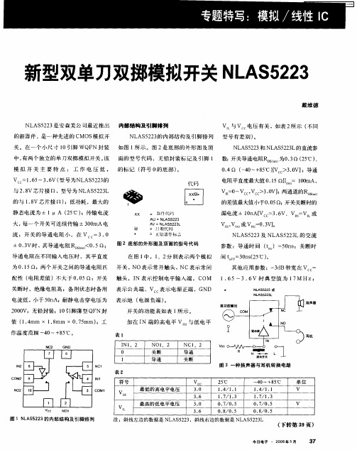
新型双单刀双掷模拟开关NLAS5223
的标记 ( 符号 0的底部 ) 。
代 码
04Q ( 4 ~+8  ̄ [ >3 0 ;导通 . 一 0 5 V C) .V]
电 阻平 直 度 最 大值 0 1 = 10 .5Q[ 0mA, Vl 0 s ~Vc, c .V】 两 通 道 的 RD。 = cVc>30 ; sn (】
驱动器 。
感 器 的 波 形 也 加 到 达 一 项 目 当 中 。硬 盘 P s T r 循 环完成 后 , as h u ATA波形 重新
由于 图 像处 理将 在 P C 中 完 成 ,
驱动器 的功能 固件 来 自F 一L 芯 片的 被 复制到 GP F的波形 存储 中。 X2 P I
关 断时 ,绝缘 电阻高 ;备 用状态时备 用 表示 公共端 ,V 表示 电源正端 ,GND
电流 低 , 小于 5 n 0 A;耐静 电击穿 电压 为 表示地 ( 电源 负端 ) 。 2 0 V;无铅封 装;l 00 0引脚 薄型 QF N封
装 ( .rm × 1 8 m × 0 7 rm ) 14 a .r a .5 a ;工 作温 度范 围 - 0 4 ~+8 ℃ 。 5 开关 的功能表 如表 l 示。 所
NL 5 2 的 内部结构 及引脚排 列 型号有差 别 ) AS 2 3 。
N AS 2 3 NL S 2 3 直 流 参 L 52 和 A 5 2 L的
关。在一个 小尺寸 l 脚 WQ 0引 FN 封 装 如 图 l 示 。 图 2是 底 部 的 外 形 图 及 顶 所
中 , 两个独立 的单 刀双掷模 拟开关 。 有 该 面 的型号 代码 ,无铅封 装标 记及引脚 l 数:开关导通 电阻R S n D(】 . f (5 、 。 为0 3 ) 2  ̄ C) 模 拟 开 关 主要 特 点 :工 作 电压 低 ,
双路单刀双掷/四路单刀双掷模拟开关

WWW t i . COm
碰 什 ,以 搜 系统 擞 静 电 破 i L L( E S1 ) )
{ = J ’ ,山 々人『 ; 眨地 降 低 r U SI j C 端I J i ; j 4 + U I : I ・ 成小。
f f l , J 处f f j 皂力 。 { 个 : 』 并 f 『 巨 提 供
肜 I 匕合 ( S M A) 十 几 仃
J , b = I I r } ,
J 。 炙
动l T s . i  ̄ 4 件映 像。
J 还l L
} 能 、r 岛精 度 f l 勺 列 { 感 J ,具 仃小 F 的竹 佬 宽 渊制功率 仉 。述 器什 4 c Ⅲ的 距 离 分 辨 私, L T I i 高竹 骶 小 于
多种 J l J 提 供 人 …l , i , J 感删 ;1 w R1 x 和 f I i
一
.
这揿 芯 片Ez I I ) C C( : 5 解决
方 案 迎 过 成 2 0 V也 器 、 … 、 U SI { 高速 ( HS ) 佑( sI 3 U) … 、. 通j 苴
( C C)霸I sI 3 U 0 【 《 卜 的V l j U S n 略f
新l , l 勺 毫 水波 软 件 I : 发 什 ( SI ) K) 包括 示 2 kv ( 人体 模 ) , ¨ 锁 i 流达y i J pe r 扣 ’ 、J l J J 过』 t 、 久J I 、过 i  ̄ , i ’ l ・ I 1 , J ¨ 】 法f ¨ 软 件 库 .它 通 过 4 ; # 1 2 o 个的 J E S I ) 7 8 嘤求 I l J . J 3 0 0 i  ̄ 1 j \ 。 简・ . 应丌 】 编 程 按 ¨( AI I ) 简化 I I 汁。
常用模拟开关芯片型号与功能和应用介绍

◆ 模 拟 断 路 器 跳 合 闸 电 源 电 压 为 DC220V 和 DC110V两档,试验前必须选择好电压和输入电压一致。
◆ 在模拟回路中设有继电器A、B、C各输出一组 转换触点,动断触点闭合或断开触点断开的触点和操 作电源完全隔离,可和微机型继电保护试验设备进行 配合。
高压模拟开关技术参数 1.跳闸时间选择:20-100ms 2.供电电源AC200V±10% 3.跳合闸操作为电源电压:DC220V、DC110V 4.合闸时间选择:20-200ms 5.跳合闸阻抗选择400Ω、200Ω、110Ω 6.模拟断路器常闭/常开接点容量为AC220V/5A
高压模拟开关应用 高压模拟开关主要用于电力系统断电保护装置或
二、常用的CMOS模拟开关集成电路
在模拟开关的集成过程中,晶体三极管和场效应 晶体管均可用来做模拟开关的有源器件,实际上,由 于场效应晶体管特性的对称性不存在残余电压等优点, 所以在模拟开关中用的最多的还是场效应晶体管。
• 开关在电路中起接通信号或断开信号的作用。最常见的 可控开关是继电器,当给驱动继电器的驱动电路加高电 平或低电平时,继电器就吸合或释放,其触点接通或断 开电路。
注意:
AD7501,AD7502,AD7503 芯片都是单向多 到一的多路开关,即信号只允许从多个 (8个) 输入端 向一个输出端传送。
单八路模拟开关CD4051
• CD4051相当于一个单刀八掷开关,开关接通哪一通 道,由输入的3位地址码ABC来决定。
• “INH”是禁止端,当“INH”=1时,各通道均不接通。 • CD4051还设有另外一个电源端VEE,以作为电平位移
模拟开关CH440芯片手册
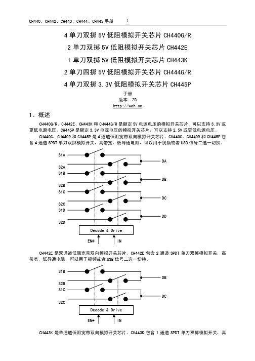
4、引脚
4.1. CH440G、CH440R、CH445P 引脚
CH440 引脚 CH445P 引脚 引脚名称 类型
引脚说明
16
14
VCC
电源
正电源
8
6、0
GND
电源
公共接地,数字信号参考地
15
13
EN#
输入
全局使能输入,低电平有效
1
15
IN
输入
单刀双掷模拟开关选择输入: 高电平选择 2#端(S2x);低电平选择 1#端(S1x)
最小值 2.1
-0.5 1.8
0 -0.3
典型值 3.3 0.1 0.6
0.1 ±0.005
7 9 28 14
最大值 3.9 5 3 0.7
VCC+0.5 5
±0.5 1.5
VCC+0.3 9 13 38 20
单位
V uA mA V V uA uA V V Ω Ω Ω Ω
6.4. 5V 开关芯片模拟开关时序参数(测试条件:TA=25℃,VCC=5V,VANA=0V)
DC S2C
Decode & Drive
EN#
IN
CH443K 是单通道低阻宽带双向模拟开关芯片。CH443K 包含 1 通道 SPDT 单刀双掷模拟开关,高
CH440、CH442、CH443、CH444、CH445 手册
2
带宽,低导通电阻,可以用于视频或者 USB 信号二选一切换。
CH0 COM
单刀四掷模拟开关的 1#端,IN1&IN0 引脚输入 00 选中
单刀四掷模拟开关的 2#端,IN1&IN0 引脚输入 01 选中
单刀四掷模拟开关的 3#端,IN1&IN0 引脚输入 10 选中
SGM3005XMS_TR圣邦微模拟开关
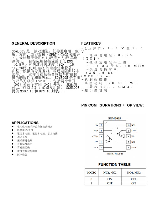
GENERAL DESCRIPTION FEATURESS GM3005是一款双通道,低导通电阻,低压,双向,单刀双掷(SPDT)CMOS模拟开关,设计用于采用+ 1.8V至+ 5.5V单电源供电。
目标应用包括受益于低RON (0.5Ω)和快速开关速度(tON = 16 ns,tOFF = 15 ns)的电池供电设备。
在整个模拟信号范围内,导通电阻曲线非常平坦。
这样可在切换音频信号时确保出色的线性度和低失真。
SGM3005是专用的双单刀双掷(SPDT),包括两个常开(NO)和两个常闭(NC)开关。
此配置可以用作双2对1多路复用器。
SGM3005提供MSOP-10和DFN-10封装。
.−低压操作:1。
8V至5.5V−低导通电阻:0。
5Ω(T Y P)−低导通电阻平坦度−–3d B带宽:30M H z−快速切换时间t O N16n st O F F15n s−轨到轨操作−典型功耗(<0.01µW)−兼容T T L/C M O S−超小型包装PIN CONFIGURATIONS(TOP VIEW)APPLICATIONS●电池供电的手持式和便携式设备●蜂窝电话/手机●笔记本电脑,笔记本电脑,掌上电脑●通讯系统●采样保持电路●音频信号路由●音视频切换●便携式测试与测量●医疗设备ORDERING INFORMATIONABSOLUTE MAXIMUM RATINGSV + to GND....................................................................- 0.3V to +6VA nalog, Digital voltage range (1)..................... - 0.3V to V + + 0.3V Continuous Current NO, NC, or COM..........................±300mA Peak Current NO, NC, or COM......................................±500mA Operating Temperature Range...........................- 40°C to +125°CJ unction Temperature...........................................................+150°CS torage Temperature.............................................- 65°C to +150°CPackage Thermal Resistance @ T A = 25℃D FN-10, θJA ........................................................................................33℃/W MSOP-10, θJA ...................................................................................205℃/WLead Temperature (soldering, 10s).......................................260°C ESD SusceptibilityH BM..........................................................................................2000V MM. (400V)Stresses beyond those listed under “Absolute Maximum Ratings” may cause permanent damage to the device. These are stressratings only, and functional operation of the device at these or any other conditions beyond those indicated in the operationals ections of the specifications is not implied. Exposure to absolute maximum rating conditions for extended periods may affectd evice reliability. (1) Signals on NC, NO, or COM or IN exceeding V+ will be clamped by internal diodes. Limit forward diode current to maximumc urrent ratings. PIN DESCRIPTIONNAMEPINFUNCTIONV + 1 Power supply GND 6 groundIN1, IN2 4,8 Digital control pin to connect the COM terminal to the NO or NC terminals COM1, COM2 3,9 Common terminal NO1, NO2 2,10 Normally-open terminal NC1, NC25,7Normally-closed terminalNote: NO, NC and COM terminalmay be an input or output.ELECTRICAL CHARACTERISTICS(V+ = +3 V ± 10%, GND = 0 V, T A = - 40°C to +125°C, unless otherwise noted. Typical values are at T A = + 25°C.)TYPICAL PERFORMANCE CHARACTERISTICSOn Response vs.FrequencyCrosstalk vs.Frequency 3-50V+ = +5VV+ = +5VT A = +25℃T A = +25℃-60-70-3-80-90-6-100-9 -1100.1 1 10 100Frequency(MHz) 0.01 0.1 1 10Frequency(MHz)Off Isolation vs.Frequency -20-30 -40 V+ = +5V T A = +25℃-50-60-70-80-90-1000.01 0.1 1 10Frequency(MHz)5TEST CIRCUITS10mAV1NO or NC COMV NO or V NCR ON = V1/10mATest Circuit 1. On ResistanceI NC(OFF) or I NO(OFF)A NO or NC COMI COM(ON)NO or NC COM AV NO or V NC V NO or V NCV COM V COM Test Circuit 2: Off Leakage Test Circuit 3: On Leakage0.1µFV+V+NO or NC COM VOUT V IN 50%50%V or V RIN300ΩC L35pF V OUT90% 90%GND tON t OFFTest Circuit 4: Switching TimesV+0.1µFV+R G ΔV OUTNO or NC COM V OUTV OUTV+ V GGND INC L1nFV IN ON ONOFF0V V INTest Circuit 5: Charge Injection6TEST CIRCUITS(Cont.)0.1µFV+V NO or V NCV+NCNO COMV OUTV IN 50%INR L300ΩC L35pFV NO or V NCGNDV OUT90%t DTest Circuit 6. Break-Before-Make Time Delay, t D0.1µFV+V+NO or NC COM VOUT SourceSignalIN R L50ΩC L5pFGNDTest Circuit 7. Off Isolation0.1µFV+V+NO or NC COMSourceSignalIN1 R L50ΩC L5pFIN2N.C.NO or NC COMV OUTGND R L50ΩC L5pFChannel To Channel Crosstalk = -20×log VNO or V NCV OUTTest Circuit 8. Channel-to-Channel Crosstalk7TEST CIRCUITS(Cont.)0.1µFV+V+NO or NC COM VOUTSource SignalIN R L50ΩC L5pFGNDTest Circuit 9. Bandwidth8PACKAGE OUTLINE DIMENSIONS MSOP-10b Ce θA2ADimensions DimensionsSymbol In Millimeters In InchesMin Max Min MaxA 0.800 1.200 0.031 0.047A1 0.000 0.200 0.000 0.008A2 0.760 0.970 0.030 0.038b 0.30 TYP 0.012 TYPc 0.152 TYP 0.006 TYPD 2.900 3.100 0.114 0.122e 0.50 TYP 0.020 TYPE 2.900 3.100 0.114 0.122E1 4.700 5.100 0.185 0.201L 0.410 0.650 0.016 0.026θ0°6°0°6°D9PACKAGE OUTLINE DIMENSIONS DFN-10NXDINDEX AREA(D/2 × E/2)40.15 CTOPVIEW0.10 C0.08 C7 SIDEVIEWD2SEE DETAIL BD/2D2/2-B-SEATINGPLANE -C-Dimensions In MillimetersSymbol Min NOM MaxA 0.70 0.75 0.80A1 0.00 0.02 0.05A3 0.20 REFb 0.18 0.25 0.30D 3.00 BSCD2 2.23 2.38 2.48E 3.00 BSCE2 1.49 1.64 1.74e 0.50 BSCK 0.20K2 0.17L 0.30 0.40 0.50L1 0.15L2 0.13N 10ND 51 2SEE DETAIL CINDEX AREA(D/2 × E/2)47N N-1e(ND-1)× e6BOTTOM VIEWeODD TERMINAL SIDEDETAIL BNX KNX b50.10 M C A B0.05 M CTERMINAL TIP5NOTES:1.尺寸和公差符合ASMEY14.5M-1994。
RS2105XN RUNIC润石模拟开关
RS2105XN描述:RS2105是双通道,低导通电阻,单刀双掷(SPDT)模拟开关,设计用于1.8V至5.5V 的电压.RS2105器件可以处理模拟和数字信号.它具有快速开关速度(50ns)和低导通电阻(0.6ΩTYP)的特点. 应用包括信号门控,斩波,调制或解调(调制解调器)以及用于模数和数模转换系统的信号多路复用.RS2105XN特点:•-3dB带宽:30MHz•高速,通常为50ns•电源范围:+ 1.8V至+ 5.5V•低导通电阻,0.6Ω(TYP)•先断后合切换•轨到轨操作•兼容TTL / CMOS•扩展的工业温度范围:-40°C至+ 125°C应用:可穿戴设备•电池供电的设备•信号门控,斩波,调制或解调(调制解调器)•便携式计算•手机ABSOLUTE MAXIMUM RATINGS (1)V+, IN to GND..................................................-0.3V to 7.0VAnalog, Digital Voltage Range (2) …......– 0.3 to (V+) + 0.3VContinuous Current NO, NC, or COM……......…... ±500mAP eak Current NO, NC, or COM……........….....…... ±800mAESD SENSITIVITY CAUTIONStorage Temperature ……….……………−65°C to +150°COperating Temperature ……….…….……−40°C to +125°CJunction Temperature................................................150°C Package Thermal Resistance @ T A = +25°CSOT23-5, SOT23-6………………….………………200°C/WMSOP-10, SOIC-8 ,TSSOP-8……….………….... 150°C/WSOIC-14, TSSOP-14………….……….……………100°C/WLead Temperature (Soldering, 10s) ……………........260°CESD SusceptibilityHBM (1000V)MM (300V)(1) Stresses above these ratings may cause permanent damage. Exposureto absolute maximum conditions for extended periods may degrade device reliability. These are stress ratings only, and functional operation of the device at these or any other conditions beyond those specified is not implied.(2) Input terminals are diode-clamped to the power-supply rails. Inputsignals that can swing more than 0.3V beyond the supply rails should be current-limited to 10mA or less. ESD损坏的范围可能从轻微的性能下降到完全的设备故障。
双通道模拟开关芯片
双通道模拟开关芯片1.引言1.1 概述在撰写双通道模拟开关芯片的文章中,我们首先需要对该主题进行一个简要的概述。
双通道模拟开关芯片是一种集成电路,具有多个通道,可以在模拟信号通路中实现信号的控制和开关功能。
通过控制引脚的状态,我们可以选择性地连接或断开不同通道之间的信号传输路径,实现对模拟信号的切换和控制。
双通道模拟开关芯片广泛应用于各种电子设备和系统中,特别是在音频、视频和通信领域中。
例如,在音频放大器中,我们可以使用双通道模拟开关芯片来实现音频信号的输入选择和输出控制;在多路视频信号处理器中,该芯片可用于切换不同视频信号源的输入和输出;另外,在无线通信系统中,双通道模拟开关芯片可以用于实现信号的切换和滤波,以提高系统性能和灵活性。
总之,双通道模拟开关芯片具有灵活的信号控制能力,可以在模拟信号通路中实现信号的切换和控制。
它在音频、视频和通信等领域有着广泛的应用前景,并为电子设备和系统的设计提供了更多的选项和功能。
在接下来的文章内容中,我们将详细介绍双通道模拟开关芯片的原理和应用,并展望其未来的发展潜力。
1.2 文章结构文章结构部分应该包括以下内容:文章结构部分主要介绍了整篇文章的组织结构和各个部分的内容安排。
本文主要分为引言、正文和结论三个部分。
在引言部分,首先进行了概述,简要介绍了双通道模拟开关芯片的背景和重要性。
接下来说明了文章结构的目的,即旨在系统性地介绍双通道模拟开关芯片的原理和应用,并提供总结与展望。
正文部分则分为两个小节。
首先,2.1节详细介绍了双通道模拟开关芯片的原理。
这一部分将从电路结构、工作原理、控制信号等方面进行深入讲解,以帮助读者充分了解该芯片的工作原理。
其次,2.2节阐述了双通道模拟开关芯片的应用。
这一部分将介绍该芯片在实际应用中的具体场景,包括音频信号切换、模拟信号传输等方面的应用案例,通过实际应用来展示该芯片的实用性和潜在市场需求。
结论部分主要包括总结和展望两个方面。
双SPDT(单刀/双掷)、低压模拟信号开关

期 间电池消耗最小。 器件的电压增益由两 个外部 电阻的分压比设 置, 精度与电阻有
电 话 :8 0 1 1 4 0 ̄8 0 7 2
htp t ,, . n l g.o a ao c r n
关 。输入 失调电压( V0s 非常小 ,仅为 ) ± 12 最大值) MAX9 3 提供微型、 .mV( 。 97
幅 )或更高 阶 Q AM 等复 杂高阶调 制应 保持 系统性 能。每个输 入端都集成 一个 阻与小于 0 0 .3Q的通道 问 匹配 , 从而使
用 中的校准 与清零需 求减到最小 。
ADI
缓 冲器以及 一个 同步 端钳位 。每 个输 出 通 道 间 的 信 号 差 异 降 至 最 低 。 另 外 , 端都 集成一个 2 l : 多路复用 器 ,用于插 AS 7 7 1 4 还具 有 0 2 ) .5(的导通 电阻平坦 入屏 幕显示 ( S 图形与输 出放大 器 , 度 。综合上 述优势 ,该 器件使总谐 波失 O D)
大大提高了设计 AD9 l Tx据 速 率 复合 调 制 。其 功 能 完 1~4m 的 最大 差 分 输 出 电流 。在 灵活性 。其可提供电池反 向( A 错误) 连接保 整, 集成 了2 d 动 态范 围输 出功率检 波 lMS s 2 5B 0 / 和 mA输 出电流下 , 功耗 仅为 护 ,还具有 器及 可变 电压衰 减器 ( VVA) 。 2 ~+ 0 O 4 V感应 电压及瞬态
双S D ( P T 单刀 /双掷 ) 低 压模 、
拟 信号开关
AS1 4 7 7兼具 0. 4Q的超低 通态 电
有 一3 d 8 Bm的载波 馈通以及 一4 d 的 1 2 个 开关组成 。 模块架构 允许任意 6 Bc 4 0 非 单边 带抑制能 力 , 将6 QAM ( 能 4 正交调 输 出组合 与任意输入 组合 的连 接 ,同时
单刀双掷开关原理

单刀双掷开关原理
单刀双掷开关是一种常用的电路开关,它可以将电路连接到两个不同的电源或负载上。
其原理是通过开关内部的可移动导电片将两组接点分别连接或断开。
单刀双掷开关一般有三个引脚,其中一个是公共引脚(COM),另外两个是固定接点引脚(NO和NC)。
当开关处于一个位置时,COM与NO连接,而COM与NC断开;而当开关处于另一个位置时,COM与NC连接,而COM与NO断开。
在一些电路应用中,我们需要根据需要切换电路连接到不同的电源或负载上。
这时候,可以使用单刀双掷开关来实现。
当开关处于一侧位置时,电路就连接到一个电源或负载上;而当开关处于另一侧位置时,电路就连接到另一个电源或负载上。
以灯泡为例,当单刀双掷开关处于一侧位置时,灯泡就会接通,电流从电源经过开关流向灯泡亮起;而当开关处于另一侧位置时,灯泡就会断开,电路中断电流无法继续流向灯泡,灯泡熄灭。
总结来说,单刀双掷开关通过内部的可移动导电片,实现将电路连接到两个不同的电源或负载上。
根据开关的位置,电路可以选择连接到一个电源或负载,或者断开电路。
这种开关在电路控制和电路切换中非常常用。
模拟开关指南

模拟开关指南TI 信号开关产品线包括高性能、低功耗的数字、模拟及专业开关。
£ PinoutsSPSTCOM GNDINV+NO 12345COM GNDINV+NC 12345TS5A1066, TS5A3166TS5A3167TS5A4596TS5A4597COM GNDINV+NO12345COM GNDINV+NC12345COMGNDNOV+IN 12345COMGNDNCV+IN 12345TS5A4594, TS12A4514, TS12A4516TS5A4595, TS12A4515, TS12A4517TS12A4514, TS12A4516N.C.N.C.V +COM GND IN N.C.NO 76582341N.C.N.C.V +COM GND IN N.C.NC 76582341TS12A4515, TS12A4517SPST x 4COM1NO2COM2IN2NO112345IN26IN27IN1IN4NO4COM4V +1413121110COM39NO38TS3A4751, TS12A44514COM1NC2COM2IN2NO112345IN36GND7IN1IN4NC4COM4V +1413121110COM39NO38TS12A44513COM1NC2COM2IN2NC112345IN36GND7IN1IN4NC4COM4V +1413121110COM39NC38TS12A44515引出脚配置£SP3TSP4T x 2NO1NO2GNDIN1V +IN2NO0COM Logic Control12348765TS5A3357, TS5A3359101171S 2123451615141312IN 21S 41S 3IN1V +2S 42S 361D 1S 12S 22S 18GND92D1EN 2EN Logic Control Logic ControlTS3A5017SPDT x 4SPDT x 2Input SelectShunt SwitchIN2IN1COM2COM1NC2NC1NO2OUT+OUT+OUT–OUT–NO1TS5A22364Audio Source 1Audio Source 28-SpeakerΩ12345109876NO2COM2NC2IN2V +NO1COM1NC1IN1GNDNO1GND NO2IN2IN1COM1NC1NC2COM2V+12345109876TS5A23157, TS5A23159, TS5A2316010117NC2123451615141312NC1NO1COM1NC4V +NO4COM46COM2NO2NC3NO38GND9COM3IN EN LogicControlTS3A5018Analog Switches PinoutsA4DCB A4321A3A2B4B3B2B1C4C3C2C1D4D3D2D1A1432 1 D /MIC_PRESENTTIP_SENSE MICp MICnC RING2 GND (1) VDD (1) RING2_SENSE B SLEEVE GND (1) VDD (1) SLEEVE_SENSEADET_TRIGGERADDR_SEL SDA SCLTSA225E12A B C12A SELV+ BMIC SLEEVECGNDRING2TS3A26746EYZP Package (Top View)模拟开关引出脚配置2x2 Crosspoint Switch for Audio Applications TS3A26746EGet samples, data sheets and app reports at: /sc/device/ts3a26746eKey Featuresr 4VQFSJPS 1433 QFSGPSNBODF (-75 dB)r $POUSPM JOQVU JT 7 MPHJD compatibler &4% QFSGPSNBODF 4-&&7& 3*/( o ±8-kV contact discharge (IEC 61000-4-2)r CVNQ NN QJUDI $41 package (1.45 x 0.95 x 0.5 mm)Applications r $FMMVMBS QIPOFT r %JHJUBM TUJMM DBNFSBT r 1%"Tr 1PSUBCMF JOTUSVNFOUBUJPOr 1PSUBCMF OBWJHBUJPO EFWJDFTThe TS3A26746E is a 2 × 2 cross-point switch that is used to interchange theground and MIC connections on a headphone connector. The ground switch has an ultra low r ON of <0.1 Ω to minimize voltage drop across it, preventing undesired increases in headphone ground reference voltage. The switch state is controlled via the SEL input. When SEL=High, GND is connected to RING2 andMIC is connected to SLEEVE. When SEL=Low, GND is connected to SLEEVE and MIC is connected to RING2. An internal 100k pull-up resistor on the SELinput sets the default state of the switch. This device effectively switches the GND and MIC lines to the appropriate coordinates with minimal signal distortion and power loss.Typical application block diagram.V +MICRIGHT LEFTTIPRING 1RING 2100 KΩSLEEVEACCESSORY DATAMIC BIAS12A B C12A SELV+ BMIC SLEEVECGNDRING2YZP Package(Top View)面向音频应用的 2 x 2 交叉点开关TS3A26746E YZP 封装(顶视图)主要特点 出众的 PSRR 性能 (-75 dB) 控制输入可兼容 1.8 V 逻辑 ESD 性能(SLEEVE 、RING2) ±8k V 接触放电 (IEC 61000-4-2) 6 焊凸、0.5 mm 间距 CSP 封装 (1.45 x 0.95 x 0.5 mm)应用蜂窝电话 数码相机个人数字助理 (PDA) 便携式仪表 便携式导航设备TS3A26746E 是一款2 x 2 交叉点开关,用于切换头戴式耳机连接器上的接地和 MIC接线。
LN3005_C南麟中文版规格书超低阻双通道 单刀双掷模拟开关

超低阻双通道单刀双掷模拟开关■产品概述LN3005是一个双通道单刀双掷模拟开关(SPDT),适用于通信系统,医疗设备和其它便携式电池供电设备。
它采用CMOS工艺,具有双向,超低阻值,低功耗,低漏电流,高速,高带宽的特点,非常适合电池供电的便携式产品采用。
其极低的开关阻抗——0.5Ω(TYP)和快速开关时间——t ON=16ns, t OFF=15ns,可以大大减少电池供电便携式产品的信号损失,改善音频及视频输出级。
LN3005在封装上采用了MSOP-10L的封装,体积小巧,节省了很多空间。
LN3005集成了两个单刀双掷开关,由两个常开NO和两个常关NC 开关组成,可以用来作为2选1的多路选择开关。
■产品特点●电压工作范围: 1.8V~5.5V●超低阻值:0.5Ω(TYP)●快速开关时间:t ON=16ns, t OFF=15ns●-3dB带宽:30MHz●超低功耗:<0.01μW●轨到轨的工作范围●TTL/CMOS兼容●小体积封装:MSOP-10L ■用途●电池供电,手提和便携式设备●手机/蜂窝式移动电话●膝上型,笔记本,掌上型PDA●通讯系统,用户交换机●医疗设备,超声波,心电图仪●测试设备,便携式仪表,数字万用表●音频和视频传输,转换●采样保持电路●数字滤波器●高速多路复用●积分复位电路等■封装●MSOP-10L■典型应用电路此应用电路仅为参考,不作为实际应用的指导,请在PCB电路设计布局中充分考虑噪声、隔离、带宽等实际情况,禁止超出芯片设计范围使用。
■ 订购信息■ 引脚配置1234V+NO1COM1IN16789NO2COM2IN2NC25NC110GNDMSOP-10L (TOP VIEW)■ 引脚分配■ 功能框图V+NO1COM1IN1NC1GNDNC2IN2COM2NO2■绝对最大额定值■电学特性参数(除非特别注明,以下参数都是在V+=5V±10%,GND=0V,T A=-40℃~+125℃测得,一般T A=25℃)(除非特别注明,以下参数都是在V+=3V±10%,GND=0V,T A=-40℃~+125℃测得,一般T A=25℃)■ 测试电路R ON =V1/10mAV NO or V NCTest Circuit 1. On ResistanceTest Circuit 2. Off Leakage Test Circuit 3. On LeakageV NO or V NCI NC(OFF) or I NO(OFF)NO or NC COMNO or NC COMV COMV COMV NO or V NCI COM(ON)AAV+V NO or V OUTLV+OUT SignalTest Circuit 4. Switching TimesTest Circuit 5. BandwidthV V■ 封装信息MSOP-10L。
TI TS3A5223 双路双刀双向模拟开关说明书
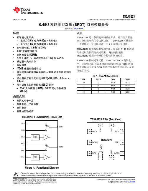
COM1COM2TS3A5223NO2V C C89102N O 11SEL2COM267COM1GND543NC1SEL1NC2TS3A5223ZHCSAQ2A –JANUARY 2013–REVISED FEBRUARY 20130.45Ω双路单刀双掷(SPDT)双向模拟开关查询样品:TS3A5223特性说明•低导通电阻开关TS3A5223是一款高速双路模拟开关,此开关具有先开后合以及双向信号切换功能。
TS3A5223可被用作–电压为3.6V 时为0.45Ω(典型值)一个双路2:1复用器或者一个1:2双路去复用器。
–电压为1.8V 时为0.85Ω(典型值)•宽电源电压:1.65V 至3.6V TS3A5223提供极低的导通电阻、很低的THD 和通道• 1.0V 兼容逻辑接口间串扰以及很高的关闭隔离。
这些特性使得•高切换带宽80MHzTS3A5223适用于音频信号传输和切换应用。
•在整个波段上,总谐波失真(THD)为0.01%TS3A5223控制逻辑支持1.0V-3.6V CMOS 逻辑电•额定最小先开后合平。
此逻辑接口可在不增加电源输出电流(ICC)的前•双向切换提下实现与大范围CPU 和微控制器的直接对接,从而•-75dB 通道至通道串扰降低了功耗。
•具有极低功耗和泄漏电流的-70dB 通道至通道关闭隔离表1.TS3A5223功能表•极小型四方扁平无引线(QFN)-10封装:1.8mm x SEL1SEL2COM COM21.4mm00NC1NC2•所有引脚上的静电放电(ESD)保护11NO1NO2–2kV 人体模型(HBM),500V 充电器件模型10NO1NC2(CDM)1NC1NO2应用范围•便携式电子产品•智能手机、平板电脑•家用电器•有线通传输通信TS3A5223FUNCTIONAL DIAGRAMTS3A5223RSW (Top View)Figure 1.Functional DiagramPlease be aware that an important notice concerning availability,standard warranty,and use in critical applications of Texas Instruments semiconductor products and disclaimers thereto appears at the end of this data sheet.TS3A5223ZHCSAQ2A–JANUARY2013–REVISED TS3A5223PIN DESCRIPTIONNAME PIN NUMBER DESCRIPTIONVCC1Postive supply Input–Connect1.65V up to3.6V supplyNC1,NO1,NC2,5,2,7,10Channel Input/Output signal PinsNO2COM1,COM23,9Channel Input/Output signal PinsGND6Ground reference pinSEL1,SEL24,8Select logic pinORDERING INFORMATION(1)T A PART NUMBER PACKAGE TOP-SIDE MARKING–40°C to85°C TS3A5223RSWR10-Pinµ-QFN Reel of3000B2_(1)For the most current package and ordering information,see the Package Option Addendum at the end of this document,or see the TIwebsite at .ABSOLUTE MAXIMUM RATINGS(1)Specified at T A=–40°C to85°C unless otherwise noted.VALUEUNITMIN MAXVCC Positive DC Supply Voltage–0.3 4.3(2)VV IN-Max Pins S1A,S1B,S2A,S2B,OUT1,OUT2,SEL1,SEL2to GND pin voltage–0.3 4.3(2)VI OUT-Max Pin OUT1,OUT2max DC current±300mAI OUT-Peak Pin OUT1,OUT2peak current(1ms pulse at10%duty cycle)±500mATotal device power dissipationP D10-µQFN RSW430mW at T A=85°CESD Rating–HBM2000V ESDESD Rating–CDM500VT A Operating free-air ambient temperature range–4085°CT J Junction temperature range–55150°CT stg Storage temperature range–55150°C (1)Stresses beyond those listed under"Absolute Maximum Ratings"may cause permanent damage to the device.These are stress ratingsonly and functional operation of the device at these conditions is not implied.Exposure to absolute-maximum-rated conditions for extended periods may affect device reliability.(2)Not rated for continuous operation,0.5%duty cycle at1kHz recommendedDISSIPATION RATINGS(1)(2)(3)DERATINGBOARD PACKAGEθJCθJA(3)FACTOR ABOVE T A<25°C T A=70°C T A=85°CT A=25ºCHigh-K10-Pinµ-QFN46°C/W93°C/W10.7mW/ºC1075W590mW430mW(1)Maximum dissipation values for retaining device junction temperature of150°C(2)Refer to TI’s design support web page at /thermal for improving device thermal performance(3)Operating at the absolute T J-max of150°C can affect reliability–for higher reliability it is recommended to ensure T J<125°C RECOMMENDED OPERATING CONDITIONSover operating free-air temperature range(unless otherwise noted)MIN MAX UNITVCC Positive DC Supply Voltage 1.65 3.6VV Max Pins NC1,NO1,NC2,NO2,COM1,COM2,SEL1,SEL2to GND pin maximum voltage0 3.6VT A Operating free-air ambient temperature range–4085ºCVCC=1.6to2.7VSEL pin Input rise and falldt/dv sec/V time limit VCC=3.0to3.6VTS3A5223 ZHCSAQ2A–JANUARY2013–REVISED FEBRUARY2013ELECTRICAL CHARACTERISTICSSpecified over the recommended junction temperature range T A=T J=–40°C to85°C Typical values are at T A=T J=25°C (unless otherwise noted).PARAMETER VCC(V)TEST CONDITIONS MIN TYP MAX UNIT DC CHARACTERISTICS3.60.8V IH High-level Input voltage SEL1,SEL2inputs 2.30.8V1.80.83.60.3V IL Low-level Input voltage SEL1,SEL2 2.30.3V1.80.33.60.450.6V S=0to VCC,IS=100mA,R ON Switch ON Resistance 2.30.60.8ΩVSEL=1.0V,0V1.80.85 1.2Difference of on-state resistance between V S=2V,0.8V,IS=100mA,VSE L=ΔR ON 3.60.05 switches 1.0V,0V3.60.10.2V S=0to VCC,IS=100mA,VSEL=R ON-FLAT ON resistance flatness 2.30.150.351.0V,0V1.80.40.65I OFF NC,NO pin leakage current when not selected 3.6V S=0.3or3.0V,VCOM=3.0or0.3V590nAI S(ON)NC,NO pin leakage current when selected 3.6V S=0.3or3.0V,VCOM=No Load460nAI SEL Select Pin input leakage current V S Vs=0or3.6V100nAI CC Quiescent supply current 3.6VSEL=0or VCC7002000nAI CCLV Supply current change 3.6VSEL=1.0V to VSEL=VCC200nA SWITCHING PARAMETERS(1)(2)3.60.1t PHL Logic high to low propagation delay 2.5R L=50Ω,C L=35pF0.2ns1.80.23.60.1t PLH Logic low to high propagation delay 2.5R L=50Ω,C L=35pF0.2ns1.80.2t ON Turn-ON time 2.3-3.6R L=50Ω,C L=35pF,VS=1.5V70nst OFF Turn-OFF time 2.3-3.6R L=50Ω,C L=35pF,VS=1.5V75nst D Break-before-make time delay 3.6R L=50Ω,C L=35pF,VS=1.5V28nsQ INJ Charge Injection 3.6C L=1nF,VS=0V40pC AC CHARACTERISTICSBW-3dB Bandwidth 1.65V-3.6V R L=50Ω,C L=35pF80MHzV ISO Channel OFF isolation 1.65V-3.6V VS=1V rms,f=100kHz–70dBV Xtalk Channel-to-Channel Cross talk 1.65V-3.6V VS=1V rms,f=100kHz–75dBR L=600Ω,VSEL=2Vpk-pk,THD Total harmonic distortion 1.65V-3.6V0.01%f=20Hz to20kHzC SEL Select Pin Input Capacitance 3.3V f=1MHz3pFNC,NO,and COM input capacitance when switchC ON 3.3V f=1MHz115pFis selectedNC,NO,and COM input capacitance when switchC OFF 3.3V f=1MHz50pFis not selected(1)Rise and Fall propagation delays,t PHL and t PLH,are measured between50%values of the input and the corresponding output signalamplitude transition.(2)Assured by characterization only.Validated during qualification.Not measured in production testing.TS3A5223ZHCSAQ2A –JANUARY 2013–REVISED FEBRUARY 2013TYPICAL CHARACTERISTICSVCC=1.8VVCC=2.3VVCC=3.0VVCC=3.6VTS3A5223ZHCSAQ2A –JANUARY 2013–REVISED FEBRUARY 2013TYPICAL CHARACTERISTICS (continued)Figure 7.Total Harmonic DistortionT A =25°CTS3A5223ZHCSAQ2A–JANUARY2013–REVISED PARAMETER MEASUREMENT INFORMATIONFigure8.ON-State Resistance(R ON)Figure9.Turn-On(t ON)and Turn-Off Time(t OFF)TS3A5223 ZHCSAQ2A–JANUARY2013–REVISED FEBRUARY2013PARAMETER MEASUREMENT INFORMATION(continued)Figure10.Break-Before-Make Time(t D)Figure11.THIRD HARMONIC DISTORTION(THD)TS3A5223ZHCSAQ2A–JANUARY2013–REVISED PARAMETER MEASUREMENT INFORMATION(continued)Figure12.Crosstalk(X TALK)Figure13.OFF Isolation(O ISO)PACKAGE OPTION ADDENDUM11-Apr-2013Addendum-Page 1PACKAGING INFORMATION(1)The marketing status values are defined as follows:ACTIVE: Product device recommended for new designs.LIFEBUY: TI has announced that the device will be discontinued, and a lifetime-buy period is in effect.NRND: Not recommended for new designs. Device is in production to support existing customers, but TI does not recommend using this part in a new design.PREVIEW: Device has been announced but is not in production. Samples may or may not be available.OBSOLETE: TI has discontinued the production of the device.(2)Eco Plan - The planned eco-friendly classification: Pb-Free (RoHS), Pb-Free (RoHS Exempt), or Green (RoHS & no Sb/Br) - please check /productcontent for the latest availability information and additional product content details.TBD: The Pb-Free/Green conversion plan has not been defined.Pb-Free (RoHS): TI's terms "Lead-Free" or "Pb-Free" mean semiconductor products that are compatible with the current RoHS requirements for all 6 substances, including the requirement that lead not exceed 0.1% by weight in homogeneous materials. Where designed to be soldered at high temperatures, TI Pb-Free products are suitable for use in specified lead-free processes.Pb-Free (RoHS Exempt): This component has a RoHS exemption for either 1) lead-based flip-chip solder bumps used between the die and package, or 2) lead-based die adhesive used between the die and leadframe. The component is otherwise considered Pb-Free (RoHS compatible) as defined above.Green (RoHS & no Sb/Br): TI defines "Green" to mean Pb-Free (RoHS compatible), and free of Bromine (Br) and Antimony (Sb) based flame retardants (Br or Sb do not exceed 0.1% by weight in homogeneous material)(3)MSL, Peak Temp. -- The Moisture Sensitivity Level rating according to the JEDEC industry standard classifications, and peak solder temperature.(4)Multiple Top-Side Markings will be inside parentheses. Only one Top-Side Marking contained in parentheses and separated by a "~" will appear on a device. If a line is indented then it is a continuation of the previous line and the two combined represent the entire Top-Side Marking for that device.Important Information and Disclaimer:The information provided on this page represents TI's knowledge and belief as of the date that it is provided. TI bases its knowledge and belief on information provided by third parties, and makes no representation or warranty as to the accuracy of such information. Efforts are underway to better integrate information from third parties. TI has taken and continues to take reasonable steps to provide representative and accurate information but may not have conducted destructive testing or chemical analysis on incoming materials and chemicals.TI and TI suppliers consider certain information to be proprietary, and thus CAS numbers and other limited information may not be available for release.In no event shall TI's liability arising out of such information exceed the total purchase price of the TI part(s) at issue in this document sold by TI to Customer on an annual basis.TAPE AND REELINFORMATION*Alldimensions are nominalDevicePackage Type Package Drawing Pins SPQReel Diameter (mm)Reel Width W1(mm)A0(mm)B0(mm)K0(mm)P1(mm)W (mm)Pin1Quadrant TS3A5223RSWR UQFNRSW103000180.09.51.161.160.54.08.0Q1PACKAGE MATERIALS INFORMATION16-Jan-2016*Alldimensions are nominal DevicePackage Type Package Drawing Pins SPQ Length (mm)Width (mm)Height (mm)TS3A5223RSWR UQFN RSW 103000184.0184.019.0PACKAGE MATERIALS INFORMATION 16-Jan-2016Pack Materials-Page 2重要声明德州仪器(TI)公司有权按照最新发布的JESD46对其半导体产品和服务进行纠正、增强、改进和其他修改,并不再按最新发布的JESD48提供任何产品和服务。
Intersil推出超低电阻双路模拟开关

Intersil推出超低电阻双路模拟开关
佚名
【期刊名称】《电子与电脑》
【年(卷),期】2005(000)012
【摘要】ISL84684,是真正在整个输入信号范围内阻抗都小于0.5Ohms的双向开关,有更低的信号损失和更低的midi/WHV信号失真,在低电源电压下有非常低的RON(接通电阻)和THD(总谐波失真).Intersil的ISL84684是一个低接通电阻、低电压、双向、双路单刀双掷(SPDT)模拟开关,专为实现音频范围内的最小失真而设计.ISL84684的信号失真值为78dB,不会降低MP3或FM的性能.
【总页数】1页(P37)
【正文语种】中文
【中图分类】TN624
【相关文献】
1.Maxim推出四路单刀/双掷模拟开关MAX4910 [J],
2.Maxim推出四路单刀/双掷模拟开关MAX4910 [J],
3.Intersil推出低压模拟开关 [J],
4.Intersil推出MightyMUX模拟开关电路 [J],
5.Intersil提供超低的导通电阻的模拟开关 [J],
因版权原因,仅展示原文概要,查看原文内容请购买。
- 1、下载文档前请自行甄别文档内容的完整性,平台不提供额外的编辑、内容补充、找答案等附加服务。
- 2、"仅部分预览"的文档,不可在线预览部分如存在完整性等问题,可反馈申请退款(可完整预览的文档不适用该条件!)。
- 3、如文档侵犯您的权益,请联系客服反馈,我们会尽快为您处理(人工客服工作时间:9:00-18:30)。
The ADG1636 is a monolithic CMOS device containing two independently selectable single-pole/double-throw (SPDT) switches. An EN input is used to enable or disable the device. When disabled, all channels are switched off. Each switch conducts equally well in both directions when on and has an input signal range that extends to the supplies. In the off condition, signal levels up to the supplies are blocked. Both switches exhibit break-before-make switching action for use in multiplexer applications.
S2B
LOGIC
07983-002
IN1 IN2 EN NOTES 1. SWITCHES SHOWN FOR A 1 INPUT LOGIC.
Figure 2. 16-Lead LFCSP
PRODUCT HIGHLIGHTS
1. 1.6 Ω maximum on resistance over temperature. 2. Minimum distortion: THD + N = 0.007%. 3. 3 V logic-compatible digital inputs: VINH = 2.0 V, VINL = 0.8 V. 4. No VL logic power supply required. 5. Ultralow power dissipation: <16 nW. 6. 16-lead TSSOP and 16-lead 4 mm × 4 mm LFCSP.
LFCSP package: 385 mA TSSOP package: 238 mA 16-lead TSSOP and 16-lead, 4 mm × 4 mm LFCSP
APPLICATIONS
Communication systems Medical systems Audio signal routing Video signal routing Automatic test equipment Data acquisition systems Battery-powered systems Sample-and-hold systems Relay replacements
3.3 V Single Supply........................................................................6 Continuous Current per Channel, S or D..................................7 Absolute Maximum Ratings ............................................................8 ESD Caution...................................................................................8 Pin Configurations and Function Descriptions ............................9 Typical Performance Characteristics ........................................... 10 Test Circuits..................................................................................... 13 Terminology .................................................................................... 15 Outline Dimensions ....................................................................... 16 Ordering Guide .......................................................................... 16
One Technology Way, P.O. Box 9106, Norwood, MA 02062-9106, U.S.A.
Tel: 781.329.4700
Fax: 781.461.3113
©2009 Analog Devices, Inc. All rights reserved.
±5 V Dual Supply ......................................................................... 3 12 V Single Supply........................................................................ 4 5 V Single Supply .......................................................................... 5
FUNCTIONAL BLOCK DIAGRAMS
ADG1636
S1A D1
S1B
IN1
IN2
S2A D2
S2B
NOTES 1. SWITCHES SHOWN FOR A LOGIC 1 INPUT.
Figure 1. 16-Lead TSSOP
07983-001
ADG1636
S1A
S2A
D1
D2
S1B
1 Ω Typical On Resistance, ±5 V, +12 V, +5 V, and +3.3 V Dual SPDT Switches ADG1636
FEATURES
1 Ω typical on resistance 0.2 Ω on resistance flatness ±3.3 V to ±8 V dual supply operation 3.3 V to 16 V single supply operation No VL supply required 3 V logic-compatible inputs Rail-to-rail operation Continuous current per channel
ADG1636
TABLE OF CONTENTS
Features .............................................................................................. 1 Applications....................................................................................... 1 General Description ......................................................................... 1 Functional Block Diagrams............................................................. 1 Product Highlights ........................................................................... 1 Revision History ............................................................................... 2 Specifications..................................................................................... 3
The ultralow on resistance of these switches make them ideal solutions for data acquisition and gain switching applications where low on resistance and distortion is critical. The on resistance profile is very flat over the full analog input range, ensuring excellent linearity and low distortion when switching audio signals.
Rev. A | Page 2 of 16
ADG1636
SPECIFICATIONS
±5 V DUAL SUPPLY
VDD = +5 V ± 10%, VSS = −5 V ± 10%, GND = 0 V, unless otherwise noted.