奋斗开发板V3.1入门手册
开发板初次使用指南

山东大学机器人电子强力驱动
打开 USB 驱动.EXE 可以看到如下画面,点击 INSTALL 即可安装(注意,此时请先不要连 接开发板与计算机)
打开检测程序,此时连接开发板与计算机,等待系统发现新硬件,让其自动安装驱动即可, 注意忽略数字认证警告。
如果安装成功既可看到 RoboElc 提示“成功打开 CH341 设备” 。注意一定要正确安装驱动, 否则无法下载程序。
绿色底板 板子跳线已经事先接插正确,当您将 USB 供电插上时,可以看到测试程序(流水灯、蜂鸣 器、数码管、DA 指示灯) 注意:8051 核心板上晶振跳线帽必须接插 以下为 AVR 核心板图片
待学习 AVR(开发板支持 ATMega16 等)时请将 8051 核心板拔下,插入 AVR 核心板,注 意方向朝上。 建议用户首先学习 8051,将内部资源等知识学习扎实再学习 AVR,我们不建议在基础知识 还没有打牢的情况下学习额外知识。 如果用户在学习好 8051 后,可以自己动手制作 STC12 系列增强型 51 核心板用于练习。
山东大学机器人电子强力驱动
螺丝螺母、跳线帽
双头 USB 线
串口延长线
10 根杜邦线
山东大学机器人电子强力驱动
底板视图(绿色)
底板视图(黑色)
软件方面:
(详见光盘) 说明: 1、首先安装 USB 驱动.EXE(USB 驱动程序) 2、然后连接 PC 与开发板,按照 USB 驱动提示操作即可 3、打开 RoboElcX 监控软件,使用该软件进行程序烧写 4、程序所有权归 WCH 公司所有 操作:
山东大学机器人电子强力驱动
RoboElc 51_AVR V1.1 开发板
初次使用指南
尊敬得用户您好!
功能详解图
开发板用户手册

开发板用户手册
开发板用户手册是一本详细介绍开发板使用方法和功能的手册。
它通常由开发板的制造商提供,用于帮助用户快速上手并了解开发板的各项功能和特性。
开发板用户手册通常包括以下内容:
1. 开发板概述:介绍开发板的基本信息,如型号、尺寸、主要组件等。
2. 开发板硬件说明:详细描述开发板的硬件组成,包括处理器、存储器、接口、扩展槽等。
3. 开发环境配置:指导用户如何正确配置开发环境,包括安装和配置开发工具、驱动程序等。
4. 开发板连接与电源配置:介绍如何正确连接开发板和其他设备,并给出电源配置建议。
5. 开发板操作指南:详细说明开发板的各项操作方法,如开机、关机、重启、调试等。
6. 开发板接口与扩展说明:介绍开发板的各种接口和扩展槽,以及如何通过这些接口和扩展槽扩展开发板功能。
7. 开发板软件开发指南:提供软件开发的相关指导,包括编程语言、开发工具、示例代码等。
8. 常见问题解答:列出一些用户常见的问题,并提供相应的解决方法。
开发板用户手册是开发板的重要参考资料,通过仔细阅读用户手册,用户可以更好地了解和使用开发板,实现自己的开发目标。
奋斗STM32开发板Tiny NRF24L01转USB虚拟串口例程手册

奋斗版 STM32 开发板例程手册———NRF24L01+转 USB 虚拟串口实验NRF24L01+转 USB 虚拟串口实验实验平台:奋斗版STM32开发板Tiny 实验内容:板子通过USB加电后,先向串口1输出一串测试数据,然后USB被PC识 别出来,虚拟出一个串口号给这个USB设备,此时可以通过在PC端的串口助手类 软件选择该串口号。
进入串口软件界面,可以通过软件无线收发一帧长度最长 为32字节的数据。
该例程可以和V3及MINI板的NRF24L01 UCGUI例程配合使用。
预先需要掌握的知识 2.4G通信模块NRF24L01 1. 产品特性2.4GHz 全球开放ISM 频段,最大0dBm 发射功率,免许可证使用 支持六路通道的数据接收 低工作电压:1.9 1.9~3.6V 低电压工作 高速率:2Mbps,由于空中传输时间很短,极大的降低了无线传输中的碰撞现象(软件设置1Mbps或者2Mbps的空中传输速率) 多频点:125 频点,满足多点通信和跳频通信需要 超小型:内置2.4GHz天线,体积小巧,15x29mm(包括天线) 低功耗:当工作在应答模式通信时,快速的空中传输及启动时间,极大的降低了电流消耗。
低应用成本:NRF24L01 集成了所有与RF协议相关的高速信号处理部分,比如:自动重发丢失数据包和自动产生应答信号等, NRF24L01的SPI接口可以利用单片机的硬件SPI口连接或用单片机I/O口进行模拟,内部有FIFO可以与各种高低速微处理器接口, 便于使用低成本单片机。
便于开发:由于链路层完全集成在模块上,非常便于开发。
自动重发功能,自动检测和重发丢失的数据包,重发时间及重发次数可软件控制 自动存储未收到应答信号的数据包 自动应答功能,在收到有效数据后,模块自动发送应答信号,无须另行编程 载波检测—固定频率检测 内置硬件CRC 检错和点对多点通信地址控制 数据包传输错误计数器及载波检测功能可用于跳频设置 可同时设置六路接收通道地址,可有选择性的打开接收通道 标准插针Dip2.54MM 间距接口,便于嵌入式应用2.基本电气特性淘宝店铺:1奋斗版 STM32 开发板例程手册———NRF24L01+转 USB 虚拟串口实验3. 引脚定义:4.工作方式NRF2401有工作模式有四种: 收发模式 配置模式 空闲模式 关机模式 工作模式由CE 和寄存器内部PWR_UP、PRIM_RX 共同控制,见下表:淘宝店铺:2奋斗版 STM32 开发板例程手册———NRF24L01+转 USB 虚拟串口实验4.1 收发模式收发模式有Enhanced ShockBurstTM收发模式、ShockBurstTM收发模式和直接收发模式三种,收发模式由器件配置字决定,具体 配置将在器件配置部分详细介绍。
开发板用户手册

开发板用户手册(原创实用版)目录1.开发板简介2.开发板硬件配置3.软件开发环境搭建4.编程实例与实践5.常见问题与解决方案6.技术支持与资源正文一、开发板简介开发板是一种集成了微处理器、存储器、输入输出接口等多种功能于一体的电子设备,主要用于软件开发和硬件调试。
本手册所介绍的开发板具有强大的功能和易用的接口,是开发者和制造商理想的选择。
二、开发板硬件配置1.微处理器:开发板搭载了高性能的微处理器,支持多任务处理和硬件加速。
2.存储器:开发板内置了大容量的存储器,可用于存储程序代码和数据。
3.输入输出接口:开发板提供了多种输入输出接口,如串口、并口、USB 等,方便连接各种外设。
4.通信接口:开发板支持多种通信协议,如 TCP/IP、UDP 等,便于实现网络通信功能。
5.扩展接口:开发板提供了可扩展接口,用户可以根据需要添加外部设备。
三、软件开发环境搭建1.安装开发板驱动:在使用开发板之前,需要先安装相应的驱动程序,以确保开发板与计算机之间的通信顺畅。
2.选择编程语言:开发板支持多种编程语言,如 C、C++、Python 等,用户可以根据自己的需求选择合适的编程语言。
3.配置编译器:根据所选编程语言,配置相应的编译器,确保编译器能够正确识别开发板的硬件接口。
4.下载程序:将编写好的程序通过串口或者其他通信接口下载到开发板上,开始实际运行。
四、编程实例与实践本部分将通过具体的编程实例,介绍如何使用开发板实现各种功能,如 LED 闪烁、按键控制、通信协议等。
五、常见问题与解决方案在使用开发板的过程中,可能会遇到一些常见的问题,如无法下载程序、通信异常等。
本部分将针对这些问题提供相应的解决方案。
六、技术支持与资源1.技术支持:开发板厂商提供免费的技术支持服务,用户可以在官方网站上查询联系方式。
2.学习资源:厂商提供了丰富的学习资源,如用户手册、编程指南、案例教程等,帮助用户快速掌握开发板的使用技巧。
通过以上介绍,相信您已经对开发板有了全面的了解。
开发板开发手册
开发板开发手册一、概述开发板是一种用于嵌入式系统开发的硬件平台,它集成了处理器、内存、输入输出接口等组件,提供了丰富的软件开发环境和工具,方便开发人员进行嵌入式系统的设计、开发和调试。
二、开发板的组成和功能1. 处理器:开发板通常采用先进的微处理器或微控制器作为核心处理器。
处理器的速度和性能决定了开发板的计算能力。
2. 内存:开发板配备了用于存储程序和数据的内存,包括闪存、RAM等。
良好的内存管理对于开发人员来说非常重要。
3. 输入输出接口:开发板提供了丰富的输入输出接口,如串口、以太网口、USB接口、GPIO等,方便连接外设设备和传感器。
4. 显示屏:一些开发板还配备了液晶显示屏或触摸屏,用于显示信息和交互操作。
5. 调试接口:开发板通常提供了调试接口,方便开发人员进行调试和性能优化。
6. 电源管理:开发板的电源管理模块可以提供稳定的电源供应,保证系统的稳定工作。
三、开发板的使用1. 开发环境搭建:在使用开发板之前,需要搭建相应的开发环境。
首先,安装相关的开发工具,如编译器、调试器等;然后,配置开发环境,包括设置路径、引入库文件等。
2. 应用开发:使用开发板进行应用开发,可以根据具体需求选择合适的开发语言和开发平台。
常见的开发语言包括C/C++、Python等,常见的开发平台包括Linux、RTOS等。
3. 软件调试:在应用开发过程中,经常需要进行软件调试,以解决程序中的bug和问题。
可以通过连接调试器和开发板,使用调试工具进行单步调试、变量监视等操作。
4. 硬件调试:对于一些需要自行设计硬件的开发板,还需要进行硬件调试。
硬件调试通常涉及到电路设计、布线、焊接等工作。
5. 应用部署:应用开发完成后,将应用程序烧录到开发板的闪存中,然后连接相应的外设设备进行测试和运行。
四、开发板的注意事项1. 硬件设计规范:如果需要自行设计硬件,需要遵守相关的设计规范,包括信号完整性、功耗管理、EMC等方面的考虑。
奋斗STM32开发板V3硬件说明书
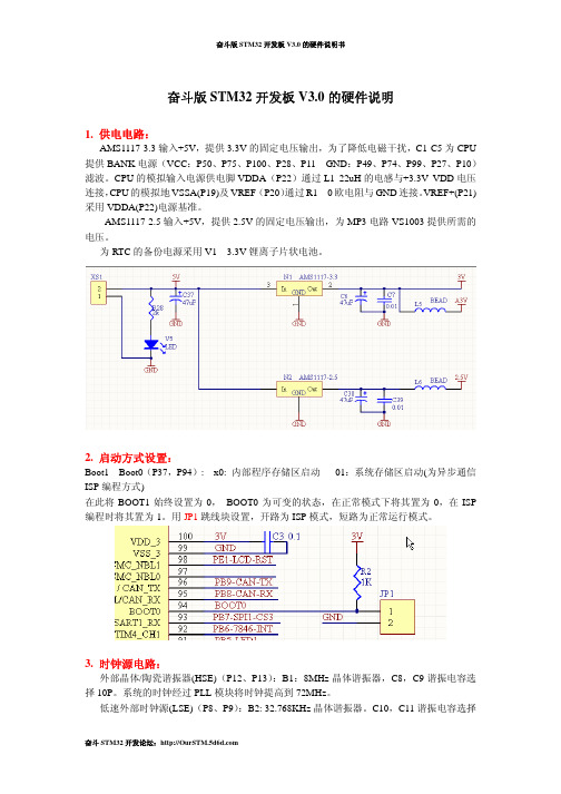
奋斗版STM32开发板V3.0的硬件说明1. 供电电路:AMS1117-3.3输入+5V,提供3.3V的固定电压输出,为了降低电磁干扰,C1-C5为CPU 提供BANK电源(VCC:P50、P75、P100、P28、P11 GND:P49、P74、P99、P27、P10)滤波。
CPU的模拟输入电源供电脚VDDA(P22)通过L1 22uH的电感与+3.3V VDD电压连接,CPU的模拟地VSSA(P19)及VREF-(P20)通过R1 0欧电阻与GND连接。
VREF+(P21)采用VDDA(P22)电源基准。
AMS1117-2.5输入+5V,提供2.5V的固定电压输出,为MP3电路VS1003提供所需的电压。
为RTC的备份电源采用V1 3.3V锂离子片状电池。
2. 启动方式设置:Boot1—Boot0(P37,P94): x0: 内部程序存储区启动01:系统存储区启动(为异步通信ISP编程方式)在此将BOOT1始终设置为0, BOOT0为可变的状态,在正常模式下将其置为0,在ISP 编程时将其置为1。
用JP1跳线块设置,开路为ISP模式,短路为正常运行模式。
3. 时钟源电路:外部晶体/陶瓷谐振器(HSE)(P12、P13):B1:8MHz晶体谐振器,C8,C9谐振电容选择10P。
系统的时钟经过PLL模块将时钟提高到72MHz。
低速外部时钟源(LSE)(P8、P9):B2: 32.768KHz晶体谐振器。
C10,C11谐振电容选择10P。
注意:根据ST公司的推荐, B2要采用电容负载为6P的晶振,否则有可能会出现停振的现象。
4. SPI存储电路:D2 SST25VF016B(2M Bytes)CPU采用SPI1端口PA7-SPI1-MOSI(P32)、PA6-SPI1-MISO (P31)、PA5-SPI1-SCK(P30)、PC4-SPI1-CS2(P33)控制读写访问, SPI1地址:0x4000 3800 - 0x4000 3BFF5. 显示及触摸接口模块:显示器采用2.4” TFT320X240LCD(控制器ILI9325), 采用CPU的FSMC功能,LCD片选CS采用FSMC_NE1(P88),FSMC_A16(P58)作为LCD的RS选择,FSMC_nWE(P86)作为LCD的/WR, FSMC_nOE(P85)作为LCD的/RD, LCD的RESET脚用CPU的PE1(P98)(LCD-RST),FSMC_D0---FSMC_D15和LCD的D1-D8 D10-D17相互连接,触摸屏接口采用SPI1接口,片选为PB7-SPI1-CS3,由于LCD背光采用恒流源芯片PT4101控制,采用了PWM控制信号控制背光的明暗, PWM信号由PD13-LIGHT-PWM来控制。
软通动力扬帆富设备开发板硬件指导手册说明书

软通动力信息技术(集团)股份有限公司目录第一章产品概述 (2)1.1适用范围 (2)1.2产品概述 (2)1.3产品特点 (2)1.4外观及接口示意图 (4)正面/背面 (4)第二章基本功能列表 (5)第三章PCB尺寸和接口布局 (6)3.1PCB尺寸图 (6)3.2接口参数说明 (6)第四章电气性能 (14)第五章使用注意事项 (15)第一章产品概述1.1.1.1适用范围扬帆开发板属于自助终端主板,普遍适用于:互动广告机、互动数字标牌、智能自助终端、智能零售终端、工控主机、机器人设备等。
1.2.1.2产品概述扬帆开发板采用瑞芯微RK3399(双Cortex-A72大核+四Cortex-A53小核)六核64位超强CPU,搭载Openharmony系统,主频最高达1.8GHz。
采用Mali-T860GPU,支持4K、H265/H264视频解码。
多路视频输出和输入,性能更强,速度更快,接口更丰富,是您在人机交互、智能终端、工控项目上的最佳选择。
1.3.1.3产品特点RK3399超强CPU,速度更快,性能更强●搭载OpenHarmony●系统支持WIFI,单天线●网口设计,支持1000M网口●内置PCI-E接口●丰富的扩展接口.六路USB接口、可扩展串口、GPIO及ADC接口,可以满足市场上各种外设的要求●高清晰度,支持eDP/HDMI OUT等接口的LCD显示屏●支持多种主流触摸屏1.4.1.4外观及接口示意图1.5.正面/背面第二章基本功能列表主要功能参数板卡尺寸146mm*104mm、板厚1.6mmCPU RK3399、六核、主频最高达1.8GHzGPU四核Mali-T860GPU高性能GPU操作系统OpenHarmony内存/存储4G(2G可选)/32G(8G/16G/64G可选)HDMI输出1个HDMI2.0a支持4K60Hz显示、支持HDCP1.4/2.2eDP输出可直接驱动1920x1080分辨率的eDP接口液晶屏视频格式支持支持MP4图片格式支持支持BMP、JPEG、PNG、GIF音频输出功放输出(支持左右声道输出,内置双4R/20W、8R/10W功放)耳机支持一路耳机接口USB接口1路USB3.0OTG、1路USB3.0Host+4路HUB串口/扩展接口1路TTL、1路DEBUG、1路IIC、4路GPIO接口、1路ADC WIFI内置WIFI、单天线以太网支持1000M以太网PCIE接口预留2.第三章PCB尺寸和接口布局2.1.3.1PCB尺寸图PCB:8层板,板厚1.6mmPCBA:L*W=146mm*104mm,MAX H=12.0+/-0.3mm螺丝孔规格:∮3.5mm x42.2.3.2接口参数说明图片标注说明:插座接口图片上圆圈处“Ο”表示第一脚。
Keil AMetal平台快速入门手册说明书

快速入门手册 (keil) AMetal 平台 UM01010101 1.0.00 Data:2019/08/18©2019 Guangzhou ZHIYUAN Micro Electronics Co., Ltd修订历史目录1. 简介 (2)2. 搭建开发环境 (3)2.1环境简介 (3)2.1.1Keil µVision 集成开发环境 (3)2.1.2仿真器 (3)2.2MDK-ARM 软件安装 (3)2.2.1MDK-ARM 软件获取 (3)2.2.2MDK-ARM 软件安装 (2)2.3支持包(PACK)的安装 (6)2.3.1支持包(PACK)的获取 (6)2.3.2支持包(PACK)的安装 (8)2.4安装J-Link 软件及J-Link 仿真器驱动 (13)2.4.1J-Link 软件安装4 (13)2.4.2J-Link 仿真器驱动安装 (15)2.5安装TKScope 软件及CK100 仿真器驱动 (19)2.5.1TKScope 软件安装 (19)2.5.2安装VC8 实时运行库装 (24)2.5.3CK100 仿真器驱动安装 (25)3. 编写应用程序 (30)3.1从模板新建工程 (30)3.1.1打开工程 (33)3.2编写程序 (34)3.3编译程序 (35)4. 调试应用程序 (38)4.1连接仿真器 (38)4.2调试相关配置 (38)4.2.1CK100 调试配置 (38)4.2.2J-Link 调试配置 (45)4.3调试应用程序 (51)4.4停止调试 (57)5. 固化应用程序 (58)5.1使用µVision5 烧写程序 (58)5.2使用其他工具烧写程序 (58)5.2.1生成程序烧写文件 (58)5.2.2使用ISP 方式烧写程序 (60)6. 免责声明 (71)©2019 Guangzhou ZHIYUAN Micro Electronics Co., Ltd 1. 简介本文主要介绍如何使用 Keil 集成开发环境对开源项目进行工程的导入、新建工程、编译链接和调试等操作,帮助用户快速掌握 Keil 集成开发环境下的应用程序开发。
开发板开发手册
开发板开发手册
开发板开发手册通常包含了开发板的基本信息、硬件配置、软件配置、开发环境搭建、示例代码等内容。
下面是一个开发板开发手册的基本结构,您可以根据自己的需要进行修改和调整。
一、开发板概述
1. 开发板简介
2. 开发板特点
3. 开发板应用领域
二、硬件配置
1. 处理器
2. 内存
3. 存储
4. 接口
5. 扩展接口
6. 外设接口
7. 电源及功耗
8. 其他配置
三、软件配置
1. 操作系统
2. 开发环境
3. 编程语言
4. 示例代码及软件库
5. 软件工具及调试器
6. 常用软件和工具包
7. 安全防护及软件升级
四、开发环境搭建
1. 硬件连接
2. 软件安装及配置
3. 开发环境初始化及设置
4. 开发环境常见问题及解决方法
五、示例代码及使用说明
1. 示例代码概述
2. 示例代码实现功能及原理说明
3. 示例代码使用说明及注意事项
4. 示例代码调试及测试方法
5. 示例代码优化及改进建议
六、常见问题及解决方法
1. 硬件问题及解决方法
2. 软件问题及解决方法
3. 其他问题及解决方法
4. 问题反馈渠道及支持服务方式
七、维护与保养
1. 定期检查硬件连接及稳定性
2. 软件更新及升级说明
3. 数据备份与恢复说明
4. 清理和保养指南。
ConnectCore MP13开发板硬件参考手册说明书
ConnectCore MP13 Development BoardTrace(if possible)Description of issueSteps to reproduceContact Digi technical support:Digi offers multiple technical support plans and service packages.Contact us at+1952.912.3444or visit us at /support.FeedbackTo provide feedback on this document,email your comments to*****************Include the document title and part number(ConnectCore MP13Development Board,900025522P)in the subject line of your email.About the ConnectCore MP13DVK Features and functionalityAbout the ConnectCore MP13DVK Safety instructionsl One10/100Ethernet with RJ-45connectorl One Gigabit Ethernet with RJ-45connectorl Two USB Host2.0interfaces through a stacked USB A type connectorl USB OTG with AB-bype micro-USB connectorl SISO IEEE802.11a/b/g/n/ac+ Bluetooth5.0with on-module U.FL or external SMA antenna connectorl PCI Express Mini Card slot supporting full and half-size cardsl MikroBus socketl XBee socket supporting XBee Cellularn User interfacel Three user LED,two of them shared with user buttonsn Dimensions:l120x160mmSafety instructionsn The ConnectCore MP13DVK cannot be guaranteed operation due to the radio link and so should not be used for interlocks in safety critical devices such as machines or automotiveapplications.n The ConnectCore MP13DVK has not been approved for use in(this list is not exhaustive): l nuclear applicationsl explosive or flammable atmospheresn There are no user serviceable components inside the ConnectCore MP13DVK.Do not modify the ConnectCore MP13in any way.Modifications may exclude the DVK from any warranty andcan cause the ConnectCore MP13to operate outside of regulatory compliance for a givencountry,leading to the possible illegal operation of the radio.n Use industry standard ESD protection when handling the ConnectCore MP13DVK.n Take care while handling to avoid electrical damage to the PCB and components.n Do not expose ConnectCore MP13DVK to water or moisture.n Use this product with the antennas specified in the ConnectCore MP13DVK user guides. ESDThe ConnectCore MP13Development Board has no additional ESD protection added to USB Host(J24)and microSD card(J13)ports.For this reason,ESD stickers have been added to thecorresponding connectors.Please consider this when using the ConnectCore MP13DevelopmentBoard.Additional ESD protection shall be added to end products using these interfaces ofConnectCore MP13SOM.About the ConnectCore MP13DVK Block diagram Block diagramAbout the ConnectCore MP13DVK Placement PlacementTop viewAbout the ConnectCore MP13DVK ConnectorsInterfaces System bootInterfaces MultimediaInterfaces Storage interface CAUTION!The RJ-45connector LEDs are connected with reversed polarity,which makesthem light when there is no Ethernet link established.The PHY should drive the cathodes ofthe diodes instead of the anodes.Interfaces User interfacesUserSolutionTo fix this issue,you must remove the current connection and tie the input clock pin of the PHY to a CPU pin that can be multiplexed as ETH2_CLK output clock.This functionality is available at twomodule pads:P19and V20.P19is currently used as part of a UART bus to keep compatibility with the ConnectCore MP15.V20is used as a standard GPIO(PA11),intended to be used as the interrupt line of SPI4,and is connected directly to an expansion header.Therefore,you must use V20to get thereference clock for the10/100MB PHY.Figure4.Default connection of SOM pad V20.Figure5.Current connection of PA11to expansion header J42.LCD_IRQ_N/PA11signal is connected through0-ohm resistor(R283)to SPI4_IRQ_N.That is why the net changes its name.Figure6.Multiplexing options of CPU pin PA11,where ETH2_CLK output reference clock for10/100MB PHY is available(AF13).To fix this connection,follow these steps:-Depopulate R283.-Depopulate R298.-Wire a cable from CPU pad side of R283to PHY pad side of R298.Figure7.Fix connection at schematic level.。
NVIDIA Jetson AGX Orin 开发板使用指南说明书

Steps for Flashing Jetson OrinContentsPurpose (3)Tools & Supplies (3)Flashing the Jetson (5)Confirming Jetpack is Successfully Installed on the Jetson (15)Downloading & Installing Cross Compilation Tools (15)Setting Up Environment Variables (15)Downloading Kernel on the Host (16)Modifying and Building Kernel on the Host (17)Flashing Newly Modified Kernel on to the Jetson (19)Complications Faced (20)Table of FiguresFigure 1 - Jetson AGX Orin Dev Kit (3)Figure 2 - Jetson Power Supply (3)Figure 3 - USB Type A to Type C Cable (4)Figure 4 - USB Type A to Micro USB Type-B Cable (4)Figure 5 - Display Port Cable (4)Figure 6 - Connecting Micro USB Type-B Cable to Jetson Micro USB Type-B Port (5)Figure 7 - Connecting USB Type-C to Jetson for Flashing (5)Figure 8 - Recovery & Restart Buttons (6)Figure 9 - SDKManager Icon (6)Figure 10 - SDK Manager (Step 1 Screen) (7)Figure 11 - CONTINUE TO STEP 02 (8)Figure 12 - STEP 02 Configurations Selected (9)Figure 13 - Accepting Terms & Conditions (9)Figure 14 - CONTINUE TO STEP 03 (10)Figure 15 - Create Folders (10)Figure 16 - Enter Password (11)Figure 17 - Verifying System Readiness to Install (11)Figure 18 - Jetson Configurations (prior to making modifications) (12)Figure 19 - Jetson Configurations (after making modifications) (13)Figure 20 - Flash the Jetson (14)Figure 21 - Accepting to Continue Installing Package (14)Figure 22 - STEP 04 SUMMARY FINALIZATION (14)Figure 23 - Finish Installation (15)Figure 24 - Recovery & Restart Buttons (19)PurposeThe purpose of this document is to outline the steps performed for flashing the Jetson Orin as well as modifying and loading a new kernel on the Jetson.Tools & SuppliesThis section lists the hardware and software tools used.•Host Desktop:o Operating System: Ubuntu•Jetson AGX Orin Developer Kit (figure obtained from online) [Figure 1]Figure 1 - Jetson AGX Orin Dev Kit•Jetson Power Supply [Figure 2]o Also need a power adaptor cable to plug into an outlet but that is not pictured in the image belowFigure 2 - Jetson Power Supply•USB Type-A 2.0 to USB Type-C cable (figure obtained from online) [Figure 3]Figure 3 - USB Type A to Type C Cable•USB Type-A 2.0 to Micro USB Type-B cable (figure obtained from online) [Figure 4]Figure 4 - USB Type A to Micro USB Type-B Cable•Display Port Cable (for the Jetson) (figure obtained from online) [Figure 5]Figure 5 - Display Port Cable•Two USB Mouse & Keyboard (one for the Jetson & one for the Host desktop) •Display Cable (for the Host desktop)•Two RJ45 cableo One to connect Host desktop to the networko Second to connect Jetson to the Host desktopFlashing the JetsonThis section outlines the steps performed to flash the Jetson.1.Connected the Micro USB Type-B end of the cable to the Micro USB port on the Jetson [Figure 6]Figure 6 - Connecting Micro USB Type-B Cable to Jetson Micro USB Type-B Port2.Connected the other end of the Micro USB cable (USB Type-A 2.0) to the Host desktop’s USBport3.Connected the USB Type-C cable to the Jetson’s USB Type-C port (designated for flashing)[Figure 7]Figure 7 - Connecting USB Type-C to Jetson for Flashing4.Connected the other end of the USB Type-C cable to the Host desktop’s USB port5.Connected an RJ45 cable to the Jetson and connected the other end to the Host desktop6.Connected the Jetson to its power supply and connected the power supply to a plug outlet7.The next set of steps (steps 8 to 34) were performed on the Host desktop8.Note: Since previously these steps have been performed, the following steps were done first:a.Removed the ~/nvidia folder by entering the command below in the terminalb.Removed the ~/Downloads/nvidia folder by entering the command below in theterminalc.Removed the NVIDIA SDKManager’s databas e file by entering the command below inthe terminal9.Put the Jetson in recovery mode by pushing the “recovery” button then pushing the “restart”button and releasing both at the same time [Figure 8]Figure 8 - Recovery & Restart Buttons10.Entered the command below on the terminal on the Host desktop to confirm the Jetson is inrecovery mode, which it was:a.NOTE: “NVIDIA” device is found, so the Jetson is in recovery mode11.Opened the SDKManager application by finding the application and clicking on it [Figure 9]Figure 9 - SDKManager Icon12.When opened, a login prompt was seen13.Logged in with my username (email) and password14.Then the following window was seen, and selected the following configurations [Figure 10]a.Product Category : Selected Jetsonb.Hardware Configuration : Disabled itc.Target Hardware : Enabled and selected JetsonAGX Orind.Target Operating System : Linux JetPack 5.0.2 (rev. 1)e.Additional SDKS: Disabled DeepStream 6.1.1Figure 10 - SDK Manager (Step 1 Screen)15.Next clicked “CONTINUE TO STEP 02” (circled in the image below) [Figure 11]Figure 11 - CONTINUE TO STEP 0216.In “STEP 02 DETAILS AND LICENSE” page, the “Jetson SDK Components” was disabled while the“Jetson Linux” was enabled as shown below [Figure 12]Figure 12 - STEP 02 Configurations Selected17.Then selected “I accept the terms and conditions of the license agreements” checkbox on thebottom of the screen (circled in the image below) [Figure 13]Figure 13 - Accepting Terms & Conditions18.Then clicked on the “CONTINUE TO STEP 03” button (circled in the image below) [Figure 14]Figure 14 - CONTINUE TO STEP 0319.The following pop up seen, selected “Create” (circled in the image below) [Figure 15]Figure 15 - Create Folders20.Then another popup was displayed requesting for administrative password, entered thepassword then clicked “OK” (circled in the image below) [Figure 16]f.NOTE: The “OK” button turns to light green after entering password in the textboxFigure 16 - Enter Password21.Then a popup is displayed that wrote “SDK Manager is verifying system readiness to install”[Figure 17]Figure 17 - Verifying System Readiness to Install22.After a few minutes, the popup disappeared and progress bars were displayed on theSDKManager’s window on the bottom of the page where the folder paths were23.Waited for a few minutes (could take about 20-30 depending on host configurations)24.After a few minutes, the following window was seen stating the SDK Manager is ready to flashthe Jetson AGX Orin module [Figure 18]Figure 18 - Jetson Configurations (prior to making modifications)25.For the setup mode, selected “Manual Setup –Jetson AGX Orin”26.For the “OEM Configuration”, selected “Pre-Config”27.Entered username and password28.For the “Storage Device”, selected “EMMC (default)”29.Below is an image of the settings selected listed in steps 25 to 28 [Figure 19]Figure 19 - Jetson Configurations (after making modifications)30.Once confirmed proper configurations are selected, clicked on “Flash” (circled in the imagebelow) [Figure 20]Figure 20 - Flash the Jetson31.NOTE: If a popup is seen stating installation is taking longer than expected, select “Yes” (circledin the image below) [Figure 21]Figure 21 - Accepting to Continue Installing Package32.After a while, the “STEP04 SUMMARY FINALIZATION” is reached and it stated the installationcompleted successfully [Figure 22]Figure 22 - STEP 04 SUMMARY FINALIZATION33.Then selected “FINISH AND EXIT” (circled in the image below) [Figure 23]Figure 23 - Finish InstallationConfirming Jetpack is Successfully Installed on the JetsonOn the Jetson, it was confirmed the Jetpack was installed and were able to successfully boot it up and log in to it.Downloading & Installing Cross Compilation ToolsFollowed the instructions in the link below to download, install, and set up the cross compilation tools on the Host desktop:https:///jetson/archives/r34.1/DeveloperGuide/text/AT/JetsonLinuxToolchain.html Setting Up Environment VariablesThe following steps were performed on the Host desktop to set up the environment variables to be used in the proceeding sections:1.Entered the commands below on the terminal to set up environment variables:Downloading Kernel on the HostThe following steps were performed on the Host desktop to download the kernel:1.Entered the command below on the terminal to change directory to the JetPack folder:~/nvidia/nvidia_sdk/JetPack_5.0.2_Linux_Jetson_AGX_ORIN_TARGETS/Linux_for_Tegra/2.Entered the command below on the terminal to create a folder named “sources” and tochange directories to it:~/nvidia/nvidia_sdk/JetPack_5.0.2_Linux_Jetson_AGX_ORIN_TARGETS/Linux_for_Tegra/sources/3.Entered the command below on the terminal to download the sources from NVIDIA:4. Entered the command below on the terminal to extract the contents from thepublic_sources.tbz2 file:5.Entered the command below on the terminal to extract the contents from thekernel_src.tbz2 file:Modifying and Building Kernel on the HostThe following steps were performed on the Host desktop to modify and build the kernel:1.Entered the command below on the terminal to create the ${KERNEL_MODULES_OUT}folder:2.Entered the command below on the terminal to change directory to the kernel folder:~/nvidia/nvidia_sdk/JetPack_5.0.2_Linux_Jetson_AGX_ORIN_TARGETS/Linux_for_Tegra/sources/kernel/ke rnel-5.03.NOTE: Some websites like the one belowhttps:///wiki/index.php/NVIDIA_Jetson_Orin/JetPack_5.0.2/Compiling_ Code/Kernelspecify to make some changes to fix some errors in the kernel. However, that was not needed for this kernel that was downloaded4. Next, the tegra_defconfig file is modified to include “CONFIG_SENSOR_LTC2990=y”in it by entering the command below to open the filea.NOTES:i.Any text editor of choice could be used here, “vi” was used in this caseii.Instructions on how to use “vi” to modify a file and save/close it is beyond the scope of this document5.Entered the command below on the terminal to create the .config file:a.NOTE: The log file could be found in the Jetson_Logs_20221026.zip file (log file name issetup_dflt_cnfg.log)6.Entered the command below on the terminal to create the BSP:bsp.log)7.Entered the command below on the terminal to install the modules:a.NOTE: The log file could be found in the Jetson_Logs_20221026.zip file (log file name ismodules_install.log)8.Entered the commands below on the terminal to create backups of existing files:9.Entered command below on the terminal to change directory to the ${KERNEL_OUT}folder:~/nvidia/nvidia_sdk/JetPack_5.0.2_Linux_Jetson_AGX_ORIN_TARGETS/Linux_for_Tegra/images/10.Entered the commands below on the terminal to copy newly created files to the designatedlocations:11.Entered the command below on the terminal to change directory to the${KERNEL_MODULES_OUT} folder:~/nvidia/nvidia_sdk/JetPack_5.0.2_Linux_Jetson_AGX_ORIN_TARGETS/Linux_for_Tegra/images/modules12.Entered the command below to compress the kernel modules folder:13.Entered the command below to apply the binaries:a.NOTE: The log file could be found in the Jetson_Logs_20221026.zip file (log file name isapply_binaries.log)Flashing Newly Modified Kernel on to the JetsonThe following steps were performed on the Host desktop to flash the newly modified kernel on the Jetson:1.Entered the command below to change directory to the location where the flash.sh script islocated:a.Current folder right now is:~/nvidia/nvidia_sdk/JetPack_5.0.2_Linux_Jetson_AGX_ORIN_TARGETS/2.Entered the command below on the terminal to check if the Jetson is in a recovery mode or not,and confirmed it wasn’t:a.NOTE: No “NVIDIA” device is found, so the Jetson is not in reco very mode3.Pushed the “recovery” button, then pushed the “restart” button and released both at the sametime to place the Jetson in recovery modeFigure 24 - Recovery & Restart Buttons4.Entered the command below on the terminal to confirm the Jetson is in recovery mode which itwas:a.NOTE: “NVIDIA” device is found, so the Jetson is in recovery mode5.Entered the command below on the terminal to flash the kernel on the Jetson:a.Complications FacedOnce the kernel completed loading, the following steps were performed:1.On the Host desktop, opened a terminal window and opened minicom by entering thecommand below:2.When in minicom, hit the enter key on the keyboard a few times which then displayed Linuxinstallation setup prompts3.Went through the setup prompts (selecting time zone, language, etc.)4.Once completed, it attempted to boot up but stopped at the following lines in the boot upmessages (seen from the serial console on minicom):a.NOTE: The log file could be found in the Jetson_Logs_20221026.zip file (log file name isBoot_Up.log)i.NOTE: Noticed a kernel panic occur in this log5.Power cycled the unit, it attempted to boot up and still stopped at the following lines:a.NOTE: NVIDIA Splash screen was displayed on the monitor, but after that, the monitorwent blank6.Attempted Step 5 with the following modifications, but still witnessed same issue:a.Connected the Jetson to the networkb.Disconnected RJ45 cable from the Jetsoni.NOTE: The log file when no RJ45 cable is connected could be found in theJetson_Logs_20221026.zip file (log file name is Second_Attempt_Boot_Up.log)21。
奋斗STM32开发板光盘资料指南

奋斗STM32开发板光盘资料指南 奋斗STM32开发板光盘资料指南奋斗STM32开发板光盘包含了奋斗嵌入式开发工作室在STM32的开发成果、文档以及外围设备的资料。
目录说明如下:JLINK V8目录:包含了适用于STM32以及其他类型ARM的JTAG仿真器JLINK V8的驱动程序以及固件修复指南和固件文件。
奋斗开发板教程目录:包含了奋斗开发板的例程手册、视频教程和入门手册等。
来自网络的STM32教程目录:包含了来自网络的对于MDK开发环境以及STM32外设的视频教学文件。
奋斗STM32开发板例程目录:7寸屏显示例程:包含了基于群创7寸屏方案的奋斗STM32显示例程奋斗STM32开发板MINI+2.4寸屏例程:包含了奋斗STM32开发板MINI的所有基础例程及针对2.4寸屏模块的显示例程(包括基于ucos ucgui的例程) 奋斗STM32开发板V3+2.4寸屏例程:包含了奋斗STM32开发板V3的所有基础例程及针对2.4寸屏模块的显示例程(包括基于ucos ucgui的例程) 奋斗STM32开发板MINI+3寸屏例程:包含了奋斗STM32开发板MINI的所有基础例程及针对3寸屏模块的显示例程(包括基于ucos ucgui的例程) 奋斗STM32开发板V3+3寸屏例程:包含了奋斗STM32开发板V3的所有基础例程及针对3寸屏模块的显示例程(包括基于ucos ucgui的例程)奋斗STM32开发板MINI+4.3寸屏例程:包含了奋斗STM32开发板MINI的所有基础例程及针对4.3寸屏模块的显示例程(包括基于ucos ucgui的例程) 奋斗STM32开发板V3+4.3寸屏例程:包含了奋斗STM32开发板V3的所有基础例程及针对4.3寸屏模块的显示例程(包括基于ucos ucgui的例程) 奋斗TINY开发板例程:包含了奋斗STM32开发板TINY的所有例程奋斗STM32开发板文档目录:包含了所有有关奋斗STM32开发板板及奋斗板模块及外设的文档。
开发板用户手册
开发板用户手册摘要:1.开发板简介2.开发板硬件配置3.软件开发环境搭建4.编程实例与实践5.常见问题与解决方案6.技术支持与资源正文:【开发板简介】开发板是一种集成了处理器、存储器、输入输出接口等多种功能于一体的计算机硬件平台,用于进行软硬件开发和测试。
本手册所介绍的开发板,具有强大的性能、丰富的外设接口以及易于使用的开发环境,是进行嵌入式系统开发、物联网应用、人工智能等领域开发的理想选择。
【开发板硬件配置】本开发板硬件配置如下:1.处理器:采用高性能的ARM 处理器,主频可达XXX MHz。
2.存储器:配备XXX MB 的DDR 内存和XXX MB 的Flash 存储,支持最大XXX MB 的MicroSD 卡扩展。
3.显示接口:支持XXX 分辨率的LCD 显示屏。
4.通信接口:具备以太网、蓝牙、Wi-Fi、LoRa 等多种通信方式。
5.输入输出接口:提供按键、LED 指示灯、串口、I2C、SPI、GPIO 等多种外设接口。
6.电源接口:支持DCXXXV 输入电压。
【软件开发环境搭建】为了方便开发者进行软件开发,我们提供了以下工具和资源:1.开发板固件:提供稳定可靠的Linux 操作系统和Android 操作系统固件。
2.编程工具:支持Keil、IAR 等主流的嵌入式开发环境。
3.调试工具:提供在线调试工具,支持断点调试、单步执行等功能。
4.开发库:提供丰富的开发库,包括网络通信、图形界面、文件系统等。
5.技术文档:提供详细的开发板用户手册、硬件参考手册、接口协议等文档。
【编程实例与实践】本手册提供了以下编程实例,供开发者学习和参考:1.LED 闪烁实验2.按键输入实验3.串口通信实验4.网络通信实验5.图形界面设计实验【常见问题与解决方案】在开发过程中,可能会遇到一些常见问题,如下所示:1.问题:无法启动开发板解决方案:检查电源线是否接触良好,检查开发板上的电源指示灯是否亮起。
2.问题:无法连接串口解决方案:检查串口线是否接触良好,尝试使用其他串口工具重新连接。
奋斗STM32开发板FM收音机例程讲解
奋斗版 STM32 开发板例程详解———FM 收音机例程FM 收音机例程实验平台:奋斗版STM32开发板V2,V3 实验内容:板子加电后,通过串口1输出操作菜单。
通过串口助手工具可以操作FM 收音机功能,具有搜索, 选台等功能。
收音机模块选用TEA5767 FM收音机模块。
这个模块的外形及引脚如下所示• 高灵敏度(使用低噪声射频输入放大器 ) • 兼容美国/欧洲(87.5 to 108 MHz)和日本(76 to 91MHz)调频波段 • 预调谐接收日本电视伴音至108 MHz • 高放自动增益控制(AGC)电路 • LC调谐振荡用低成本固定芯片 • 调频中频选择在内部完成,中频免调 • 三种振荡基准频率输入32.768K、13M、 6.5M • 锁相环调谐系统 • 由总线模式管脚来选择I2C总线模式或三线模式 • 由总线输出7位中频计数,由总线输出4位电平 • 软静音,立体声消噪(SNC),高电平切割 (HCC) • 软静音,立体声消噪(SNC),高电平切割 (HCC)能通过总线关断 •免调谐立体声解码器,自动搜索调谐功能淘宝店铺:1奋斗版 STM32 开发板例程详解———FM 收音机例程1. 应用实例1.1. 设计要求板子加电后,通过串口1的输出输入信息可以操作FM收音机搜索,选台。
1.2 硬件电路设计如下图所示STM32F103VET6的47脚48脚作为I2C口线,控制TEA5767,完成收音机操作功 能。
电路TDA1308作为音频功率放大电路,完成音频到耳机插座的放大输出, 耳机线的地线在此时同时充当了收音机的天线。
D9的3脚接地表示工作在I2C模 式。
1.3 软件程序设计软件思路: 由于STM32的I2C固件库BUG, 因此我们用STM32的PB10, PB11模拟I2C的SCL和SDA时序。
来淘宝店铺: 2奋斗版 STM32 开发板例程详解———FM 收音机例程控制TEA5767。
奋斗开发板MINI入门手册

奋斗版STM32开发板MINI入门手册基础知识篇作为STM32的初学者,首先需要了解硬件资源, STM32是意法半导体推出的基于CoreTex-M3内核的32位ARM, 目前主要有5个系列、奋斗版STM32开发板的MINI及V3选用了STM32F103VET6作为开发板的MCU。
这个芯片属于STM32F103系列的高容量芯片, QFP100封装, 主要特征:64K片内SRAM 512K片内FLASH。
具有FSMC接口(并行外设外设接口,TFT模块就是通过这个连接的),SDIO 4位接口(SD 卡的专用接口,速度更高)。
之所以选用这个芯片作为开发板的MCU,主要是基于以下几点:1-------容量大,是STM32系列里,容量最大的芯片2-------体积适中 QFP100脚封装,从大型设备到手持设备都可以选用。
3-------FSMC接口 由于板上设计有TFT模块, 因此选用具有FSMC接口的芯片是必然的。
4-------SDIO接口 作为一个嵌入式的平台,大容量SD存储是必须考虑的, 可以在SD上建立文件系统及大容量文件存取。
5-------性价比高, 该芯片的批量采购价格在30元左右,渠道稳定,适合工程选用。
很多用户先前都是从51平台转过来的, 对单片机的经验还停留在51带给我们的简单易用上,51单片机的资源简单,且口线定义唯一。
相对高端的51型单片机(如SILICON C8051F系列,AVR等)可以做到一定的口线复用(就是一个口线可以具有多种复用功能),51在处理对计算速度及控制速度相对不高的应用,还是具有很好的性价比及应用性。
近几年,随着应用技术的发展, 产品对嵌入式技术要求越来越高,51单片机已经不能满足复杂嵌入式应用要求, 在ARM技术发展过程中,coretex-M3内核应运而生,它的各项能力使得它成为微控领域之王,STM32是这种内核的产物, 是目前coretex-M3内核平台里最具性价比的平台,可以预见,未来几年里,STM32会很快占据微控平台市场。
努沃通 M031TC 开发板用户手册说明书

M-m UARM ® Cortex ®-M32-bit MicrocontrollerNuMaker-M031TC User ManualNuMicro ®M031 SeriesThe information described in this document is the exclusive intellectual property ofNuvoton Technology Corporation and shall not be reproduced without permission from Nuvoton.Nuvoton is providing this document only for reference purposes of NuMicro microcontroller based systemdesign. Nuvoton assumes no responsibility for errors or omissions.All data and specifications are subject to change without notice.For additional information or questions, please contact: Nuvoton Technology Corporation.Table of Contents1Overview (6)1.1NuMaker-M031TC Features (6)2NuMaker-M031TC Overview (8)2.1Front View (8)Rear View (9)2.22.3Arduino UNO Compatible Extension Connectors (10)Pin Assignment for Extension Connectors (12)2.42.5System Configuration (14)2.5.1VIN Power Source (14)2.5.2 5 V Power Sources (14)2.5.3 3.3 V Power Sources (14)2.5.4 1.8V Power Sources (15)2.5.5Power Connectors (15)2.5.6USB Connectors (15)2.5.7Power Switches (15)2.5.8Power Supply Models (16)2.5.9Ammeter Connector (19)2.5.10Extension Connectors (19)2.5.11Push-Buttons (19)2.5.12LEDs (20)2.6Nu-Link2-Me (20)2.7PCB Placement (21)3Quick Start (22)3.1Toolchains Supporting (22)3.2Nuvoton Nu-Link Driver Installation (22)3.3BSP Firmware Download (24)3.4Hardware Setup (24)3.5Find the Example Project (26)3.6Execute the Project under Toolchains (26)3.6.1Keil MDK (26)3.6.2IAR EWARM (30)3.6.3NuEclipse (31)4NuMaker-M031TC Schematics (32)M-m UNu-Link2-Me ........................................................................................... 32 4.1 M031 Platform ......................................................................................... 33 4.2Extension Connector (34)4.35REVISION HISTORY (35)List of FiguresFigure 1-1 NuMaker-M031TC Board (6)Figure 2-1 Front View of NuMaker-M031TC (8)Figure 2-2 Rear View of NuMaker-M031TC (9)Figure 2-3 Arduino UNO Compatible Extension Connectors (10)Figure 2-4 M031TC1AE Extension Connectors (12)Figure 2-5 External Power Supply Sources on Nu-Link2-Me (16)Figure 2-6 External Power Supply Sources on M031 Platform (17)Figure 2-6 Separate the Nu-Link2-Me from NuMaker-M031TC (18)Figure 2-7 Wiring between Ammeter Connector and Ammeter (19)Figure 2-8 Front Placement (21)Figure 2-9 Rear Placement (21)Figure 3-1 Nu-Link USB Driver Installation Setup (22)Figure 3-2 Nu-Link USB Driver Installation (23)Figure 3-3 Open VCOM Function (24)Figure 3-4 ICE USB Connector (24)Figure 3-5 Device Manger (25)Figure 3-6 PuTTY Session Setting (25)Figure 3-7 Template Project Folder Path (26)Figure 3-8 Warning Message of “Device not found” (26)Figure 3-9 Project File Migrate to Version 5 Format (27)Figure 3-10 Debugger Setting in Options Window (27)Figure 3-11 Programming Setting in Options Window (28)Figure 3-12 Compile and Download the Project (28)Figure 3-13 Keil MDK Debug Mode (29)Figure 3-14 Debug Message on Serial Port Terminal Windows (29)Figure 3-15 IAR EWARM Window (30)Figure 3-16 Compile and Download the Project (30)Figure 3-17 IAR EWARM Debug Mode (31)Figure 3-18 Debug Message on Serial Port Terminal Windows (31)Figure 4-1 Nu-Link2-Me Circuit (32)Figure 4-2 M031 Platform Circuit (33)Figure 4-3 Extension Connectors Circuit (34)List of TablesTable 2-1 Arduino UNO Extension Connectors and M031TC1AE Mapping GPIO List (11)Table 2-2 M031TC1AE Full-pin Extension Connectors and GPIO Function List (13)Table 2-3 Vin Power Source (14)Table 2-4 5V Power Sources (14)Table 2-5 3.3 V Power Sources (14)Table 2-6 1.8V Power Sources (15)Table 2-7 Power Connectors (15)Table 2-8 USB Connectors (15)Table 2-9 Power Switches (15)Table 2-10 Supply External Power through Nu-Link2-Me (16)Table 2-11 Supply External Power for M031 platform (18)Table 2-12 Ammeter Connector (19)Table 2-13 Extension Connectors (19)Table 2-14 Push-Buttons (19)Table 2-15 LEDs (20)Table 2-16 VCOM Function of Nu-Link2-Me (20)M-mU1 OVERVIEWThis user manual is aimed to give users a fast introduction to the use of NuMaker-M031TC board.The NuMaker-M031TC consists of two parts, a M031 platform and an on-board Nu-Link2-Me debugger and programmer. The NuMaker-M031TC allows users to quickly develop and easily program and debug application.The NuMaker-M031TC offers M031TC1AE full pins extension connectors, Arduino UNO compatible extension connectors and diversified power supply option. It is an easy-to-develop platform for user to expand the functionality and build the applications. The NuMaker-M031TC also provides an ammeter connector, allows user to monitor the microcontroller’s power consumption during development.The Nu-Link2-Me is a debugger and programmer that supports on-line programming and debugging through SWD interface. The on-board 16 Mbit SPI Flash allows it able to off-line programming the target microcontroller. Nu-Link2-Me provides virtual COM port (VCOM) function to print out messages on PC. Nu-Link2-Me can be separated from NuMaker-M031TC, allowing user to use as a mass production programming tool.Figure 1-1 NuMaker-M031TC Board1.1NuMaker-M031TC Features●NuMicro® M031TC1AE used as main microcontroller with function downward compatiblewith:◆M031TC1AE◆M031EC1AE◆M031FC1AE●M031TC1AE full pins extension connectors●Arduino UNO compatible extension connectors●Ammeter connector for measuring the microcontroller’s power consumption●Fixable board power supply:◆External V DD power connector◆Arduino UNO compatible extension connector Vin◆USB power connector on M031 platform◆ICE USB connector on Nu-Link2-Me●On-board Nu-Link2-Me debugger and programmer:◆Debug through SWD interface◆On-line/off-line programming◆Virtual COM port functionM-mU2NUMAKER-M031TC OVERVIEWFront View2.1ICE USB Connector VCOM SwitchReset Button ICE Status LEDOff-line Program ButtonUSB Power Connector Power LED PB14 LEDV DD SwitchTarget Chip: M031TC1AETarget Chip Extension Connector Arduino UNO Compatible Extension ConnectorExternal V DD ConnectorNu-Link2-MeAmmeter ICE Chip: M48SSIDAE External V SS ConnectorM031 PlatformFigure 2-1 Front View of NuMaker-M031TCFigure 2-1 shows the main components and connectors from the front side of NuMaker-M031TC. The following lists components and connectors from the front view:● Target Chip: M031TC1AE(U1) ● USB Power Connector(J2)● Arduino UNO Compatible Extension Connectors (NU1, NU2, NU3, NU4) ● M031 Extension Connectors (JP3, JP4, JP5 and JP6) ●External V DD Power Connector(JP1) ● External V SS Power Connector(JP2) ● VDD Switch(SW2)● Ammeter Connector(AMMETER) ● Reset Button(SW1)● Power LED and PB14 LED(LEDG1 and LEDR1) ●Nu-Link2-Me ◆ VCOM Switch◆ ICE Chip: M48SSIDAE(ICEU2) ◆ ICE USB Connector(ICEJ3)◆ ICE Status LED(ICES0,ICES1, ICES2, ICES3) ◆Off-line Program Button(ICESW1)2.2Rear ViewFigure 2-2 shows the main components and connectors from the rear side of NuMaker-M031TC.The following lists components and connectors from the rear view:●Nu-Link2-Me◆MCUVCC Power Switch (ICEJPR1)◆ICEVCC Power Switch (ICEJPR2)ICEVCC Power SwitchMCUVCC Power SwitchFigure 2-2 Rear View of NuMaker-M031TCNUMAKER-M031TC USER MANUAL M-m U2.3Arduino UNO Compatible Extension ConnectorsFigure 2-3 shows the Arduino UNO compatible extension connectors.Figure 2-3 Arduino UNO Compatible Extension ConnectorsNUMAKER-M031TC USER MANUALM-mUTable 2-1 Arduino UNO Extension Connectors and M031TC1AE Mapping GPIO ListPin Assignment for Extension Connectors2.4The NuMaker-M031TC provides the M031TC1AE target chip onboard and full pins extension connectors (JP3, JP4, JP5 and JP6). The Figure 2-4 shows the M031TC1AE extension connectors.JP3Pin1 ~ Pin8JP6Pin25 ~ Pin32JP5Pin9 ~ Pin18JP4Pin19 ~ Pin24Figure 2-4 M031TC1AE Extension ConnectorsNUMAKER-M031TC USER MANUAL M-m U2.5System Configuration2.5.1 VIN Power SourceTable 2-3 presents the Vin power source.Table 2-3 Vin Power Source 2.5.2 5 V Power SourcesTable 2-4 presents the 5 V power sources.Table 2-4 5V Power Sources 2.5.3 3.3 V Power SourcesTable 2-5 presents the 3.3 V power sources.Table 2-5 3.3 V Power SourcesM-mU2.5.4 1.8V Power SourcesTable 2-6 presents the 1.8 V power source.Table 2-6 1.8V Power Sources2.5.5 Power ConnectorsTable 2-7 presents the power connectors.Table 2-7 Power Connectors2.5.6 USB ConnectorsTable 2-8 presents the USB connectors.Table 2-8 USB Connectors2.5.7 Power SwitchesTable 2-9 presents the power switches.Table 2-9 Power Switches2.5.8 Power Supply Models2.5.8.1External Power Supply through Nu-Link2-Me to Target ChipThe external power supply source on Nu-Link2-Me is shown in Figure 2-5.ICE USB Connector (ICEJ3)Nu-Link2-MeFigure 2-5 External Power Supply Sources on Nu-Link2-MeTo use ICEJ3 as external power supply source with Nu-Link2-Me, please follow the below steps:1. Solder the resistor on ICEJPR1 (MCUVCC) depends on the target chip operating voltage.2. Solder the resistor on ICEJPR2 (ICEVCC) depends on the ICE chip operating voltage.3. Switch the SW2 to OFF.4. Connect the external power supply to JP1.Table 2-10 presents all power models when supplies external power through Nu-Link2-Me. The Nu-Link2-Me external power sources are highlighted in yellow.Table 2-10 Supply External Power through Nu-Link2-MeM -m UExternal Power Supply through M031 platform to Target Chip 2.5.8.2The external power supply sources on M031 platform are shown in Figure 2-6.USB Power Connector (J2)NU1 pin8 (Vin)External V DD Connector (JP1)External V SS Connector (JP2)Figure 2-6 External Power Supply Sources on M031 PlatformTo use Vin or J2 as external power supply source, please follow the below steps:1. Switch the SW2 depends on the target chip operating voltage.2. Remove the resistor on ICEJPR1 (MCUVCC).3. Solder the resistor on ICEJPR2 (ICEVCC) depends on the ICE chip operating voltage.4. Connect the external power supply to Vin or J2.To use JP1 as external power supply source, please follow the below steps:1. Switch the SW2 to OFF.2. Remove the resistor on ICEJPR1 (MCUVCC).3. Solder the resistor on ICEJPR2 (ICEVCC) depends on the ICE chip operating voltage.4. Connect ICEJ3 to PC.5. Connect the external power supply to JP1.6.To use Vin or J2 as external power supply source with Nu-Link2-Me separated from NuMaker- M031TC, please follow the below steps:1. Switch the SW2 depends on the target chip operating voltage.2. Separate the Nu-Link2-Me from NuMaker- M031TC.3. Connect the external power supply to Vin or J2.To use JP1 as external power supply source with Nu-Link2-Me separated from NuMaker-M031TC, please follow the below steps:1. Switch the SW2 to OFF.2. Separate the Nu-Link2-Me from NuMaker-M031TC.3. Connect the external power supply to JP1.USB Power Connector (J2)NU1 pin8 (Vin)External V DD Connector (JP1)External V SS Connector (JP2)Separate Nu-Link2-Me""Figure 2-7 Separate the Nu-Link2-Me from NuMaker-M031TCTable 2-11 presents all power models when supplies external power through M031 platform. TheTable 2-11 Supply External Power for M031 platformM -m U2.5.9 Ammeter ConnectorTable 2-12 presents the ammeter connector.Table 2-12 Ammeter ConnectorUSB Power Connector (J2)NU1 pin8 (Vin)External V DD Connector (JP1)External V SS Connector (JP2)Separate Nu-Link2-Me""2.5.10 Extension ConnectorsTable 2-13 presents the extension connectors.Table 2-13 Extension Connectors2.5.11 Push-ButtonsTable 2-14 presents the push-buttons.Table 2-14 Push-Buttons2.5.12 LEDsTable 2-15 presents the LEDs.Table 2-15 LEDs2.6Nu-Link2-MeThe Nu-Link2-Me is a debugger and programmer that supports on-line programming and debugging through SWD interface. The on-board 16 Mbit SPI Flash allows it to off-line program the target microcontroller. Additionally, the Nu-Link2-Me provides virtual COM port (VCOM) function to print out messages on PC. Table 2-16 presents how to set the VCOM function by ICESW2.Table 2-16 VCOM Function of Nu-Link2-MeNUMAKER-M031TC USER MANUALM-mUPCB Placement2.7Figure 2-9 and Figure 2-10 show the front and rear placement of NuMaker-M031TC.Figure 2-9 Front PlacementFigure 2-10 Rear Placement3 QUICK START3.1Toolchains SupportingInstall the preferred toolchain. Please make sure at least one of the toolchains has been installed.●KEIL MDK Nuvoton edition M0/M23●IAR EWARM●NuEclipse (GCC)(Windows)●NuEclipse (GCC)(Linux)3.2Nuvoton Nu-Link Driver InstallationDownload and install the latest Nuvoton Nu-Link Driver.●Download and install Nu-Link_Keil_Driver when using Keil MDK.●Download and install Nu-Link_IAR_Driver when using IAR EWARM.●Skip this step when using NuEclipse.Please install the Nu-Link USB Driver as well at the end of the installation. The installation is presented in Figure 3-1 and Figure 3-2.Figure 3-1 Nu-Link USB Driver Installation SetupNUMAKER-M031TC USER MANUAL M-m U Figure 3-2 Nu-Link USB Driver Installation3.3BSP Firmware DownloadDownload and unzip the Board Support Package (BSP).Hardware Setup3.41. Open the virtual COM (VCOM) function by changing Nu-Link2-Me VCOM Switch No. 1 and 2 toON.Figure 3-3 Open VCOM Function2. Connect the ICE USB connector shown in Figure 3-4 to the PC USB port through USB cable.Figure 3-4 ICE USB Connector3. Find the “Nuvoton Virtual COM Port” on the Device Manger as Figure 3-5.NUMAKER-M031TC USER MANUALM-m UFigure 3-5 Device Manger4. Open a serial port terminal, PuTTY for example, to print out debug message. Set the speed to115200. Figure 3-6 presents the PuTTY session setting.Figure 3-6 PuTTY Session SettingFind the Example Project3.5Use the “Template” project as an example. The project can be found under the BSP folder as shown in Figure 3-7.Figure 3-7 Template Project Folder Path3.6Execute the Project under ToolchainsOpen and execute the project under the toolchain. The section 3.6.1, 3.6.2, and 3.6.3 describe the steps of executing project in Keil MDK, IAR EWARM and NuEclipse, respectively.3.6.1 Keil MDKThis section provides steps to beginners on how to run a project by using Keil MDK.1. Double click the “Template.uvproj” to open the project.Note: If Figure 3-8 warning message jumps out, please migrate to version 5 formats as shown in Figure 3-9. The “.uvproj” filename extension will change to “.uvprojx”.Figure 3-8 Warning Message of “Device not found”NUMAKER-M031TC USER MANUALM-m U123Figure 3-9 Project File Migrate to Version 5 Format2. Make sure the debugger is “Nuvoton Nu-Link Debugger ” as shown in Figure 3-10 and Figure 3-11.Note: If the dropdown menu in Figure 3-10 does not contain “Nuvoton Nu-Link Debugger ” item, please rework section 3.2.21Figure 3-10 Debugger Setting in Options Window345Figure 3-11 Programming Setting in Options Window3. Rebuild all target files. After successfully compile the project, download code to the flash memory.Click “Start/Stop Debug Section” button can enter debug mode.13 24 1. Rebuild3. Download4. Start/Stop Debug2. Successfully compileFigure 3-12 Compile and Download the Project4. Figure 3-13 shows the debug mode under Keil MDK. Click “Run” and the debug message will beprinted out as shown in Figure 3-14. User can debug the project under debug mode by checkingNUMAKER-M031TC USER MANUALM-mUsource code, assembly language, peripherals ’ registers, and setting breakpoint, step run, value monitor, etc.2. Stop 3 1 21. Run3. ResetFigure 3-13 Keil MDK Debug ModeFigure 3-14 Debug Message on Serial Port Terminal Windows3.6.2 IAR EWARMThis section provides steps to beginners on how to run a project by using IAR EWARM.1. Double click the “Template.eww” to open the project.2. Make sure the toolbar contain “Nu-Link” item as shown in Figure 3-15.Note: If the toolbar does not contain “Nu-Link” item, please rework section 3.2.Figure 3-15 IAR EWARM Window3. Make target file as presented in Figure 3-16. After successfully compile the project, downloadcode to the flash memory and enter debug mode.1321. Make3. Download and Debug2. Successfully compileFigure 3-16 Compile and Download the ProjectNUMAKER-M031TC USER MANUALM-mU4. Figure 3-17 shows the debug mode under IAR EWARN. Click “Go ” and the debug message willbe printed out as shown in Figure 3-18. User can debug the project under debug mode by checking source code, assembly language, peripherals ’ registers, and setting breakpoint, step run, value monitor, etc.1 2 31. Go 3. Reset2. BreakFigure 3-17 IAR EWARM Debug ModeFigure 3-18 Debug Message on Serial Port Terminal Windows3.6.3 NuEclipseFor more information about how to use NuEclipse, please refer to the NuEclipse User Manual.4 NUMAKER-M031TC SCHEMATICS4.1Nu-Link2-MeFigure 4-1 shows the Nu-Link2-Me circuit. The Nu-Link2-Me is a debugger and programmer that supports on-line programming and debugging through SWD interface.Nu-Link2-MeFigure 4-1 Nu-Link2-Me Circuit4.2M031 PlatformFigure 4-2 shows the M031 platform circuit.NUMAKER-M031TC USER MANUAL M-m UFigure 4-2 M031 Platform Circuit4.3Extension ConnectorFigure 4-3 shows extension connectors of NuMaker-M031TC.Figure 4-3 Extension Connectors Circuit5 REVISION HISTORY2019.02.20 1.00 1. Initially issued.M-mUImportant NoticeNuvoton Products are neither intended nor warranted for usage in systems or equipment, any malfunction or failure of which may cause loss of human life, bodily injury or severe property damage. Such applications are deemed, “Insecure Usage”.Insecure usage includes, but is not limited to: equipment for surgical implementation, atomic energy control instruments, airplane or spaceship instruments, the control or operation of dynamic, brake or safety systems designed for vehicular use, traffic signal instruments, all types of safety devices, and other applications intended to support or sustain life.All Insecure Usage shall be made at customer’s risk, and in the event that third parties lay claims to Nuvoton as a result of customer’s Insecure Usage, custome r shall indemnify the damages and liabilities thus incurred by Nuvoton.。
51单片机开发板使用手册
STU_MAIN单片机开发板使用手册第一章STU_MAIN 单片机开发板简介 (2)1.1 单片机开发板概述 (2)1.2 单片机开发板载资源介绍 (2)1.3 STU_MAIN 单片机开发板接口说明 (4)1.4 如何开始学习单片机 (5)第二章软件使用方法 (6)2.1 KEIL 软件的使用方法 (6)2.2 STC-ISP 软件的安装与使用 (13)2.3 使用USB 口下载程序时设置步骤 (18)第三章STU_MAIN 开发板例程详细介绍 (21)3.1 准备工作 (21)3.2安装STC-ISP下载程序 (21)3.3 闪烁灯 (22)3.4 流水灯 (23)3.5 单键识别 (25)3.6 利用定时器和蜂鸣器唱歌 (28)3.7 DS18B20 温度测量显示实验 (31)3.8LCD1602 字符液晶显示 (36)3.9串口通讯实验 (39)3.10 基于DS1302的多功能数字钟实验 (41)3.11 EEPROM X5045实验 (47)第一章STU_MAIN 单片机开发板简介1.1 单片机开发板概述STU_MAIN 单片机开发板是经过精心设计开发出的多功能MCS-51 单片机开发平台。
该开发板集常用的单片机外围资源、串口调试下载接口于一身,可以让您在最短的时间内,全面的掌握单片机编程技术。
该开发板特别适合单片机初学者、电子及通信等专业的课程设计以及电子爱好者自学使用。
STU_MAIN 单片机开发板可作为单片机课程的配套设备,课程从最基本的预备知识开始讲起,非常详细的讲解KEIL 编译器的使用,包括软件仿真、测定时间、单步运行、全速运行、设置断点、调试、硬件仿真调试、变量观察等,整个过程全部用单片机的C 语言讲解,从C 语言的第一个主函数MAIN 讲起,一步步一条条讲解每一个语法、每条指令的意思,即使对单片机一巧不通,对C 语言一无所知,通过本课程的学习也可以让你轻松掌握MCS-51 单片机的C 语言编程。
- 1、下载文档前请自行甄别文档内容的完整性,平台不提供额外的编辑、内容补充、找答案等附加服务。
- 2、"仅部分预览"的文档,不可在线预览部分如存在完整性等问题,可反馈申请退款(可完整预览的文档不适用该条件!)。
- 3、如文档侵犯您的权益,请联系客服反馈,我们会尽快为您处理(人工客服工作时间:9:00-18:30)。
硬件篇:
奋斗版 STM32 开发板 V3.1 板,可选配奋斗嵌入式开发工作室的 2.4 寸(240X320)TFT 显示器、3 寸(240X400)TFT 显示器,4.3 寸(480X272)TFT 显示器及 7 寸(800X480)显 示方案。外接电源都是 5V,在学习过程中,可以用所配的 USB 线通过电脑给板子提供电源。 但也有可能由于一些电脑的 USB 供电能力太弱,提供不了足够的电流,此时就需要外接 5V 电源给板子供电了,否则会造成板子工作不正常的现象。V3 板可以通过电源插座提供 5V 接 口。 请配合原理图及硬件手册来了解奋斗 STM32 开发板的详细资源。
奋斗嵌入式开发工作室
奋斗版 STM32 开发板文档
奋斗开发板配 4.3 寸 TFT 显示器: 该模块是奋斗版 STM32 开发板 V3 及 MINI 板的配套模块,采用 STM32 的 FSMC 接口模式。
SSD1963 作为控制驱动器,显示速度更快。4.3 寸屏, 分辨率 480X272, 64K 色,数据接 口 16 位, 背光驱动采用白光驱动器提供背光用的横流源, 使背光更加均匀,背光明暗控 制采用 TTL 电平或者 PWM 模式控制。屏上带电阻式触摸屏, 模块板上带 SPI 控制方式的触 摸屏控制电路。
奋斗嵌入式开发工作室
奋斗版 STM32 开发板文档
嵌入式应用要求, 在 ARM 技术发展过程中,coretex-M3 内核应运而生,它的各项能力使得 它成为微控领域之王,STM32 是这种内核的产物, 是目前 coretex-M3 内核平台里最具性价 比的平台,可以预见,未来几年里,STM32 会很快占据微控平台市场。
奋斗嵌入式开发工作室
奋斗版 STM32 开发板文档
httpபைடு நூலகம்//
奋斗嵌入式开发工作室
奋斗版 STM32 开发板文档
开发环境篇:
奋斗版 STM32 开发板 MINI 及 V3 的例程工程编写均基于 RealView MDK-ARM3.80a 开发 环境,工程里所包含的库大部分采用了 STM32 标准库 3.5.0,MDK 开发环境支持 JLINK、ULINK、 ST-LINK 的在线仿真及下载。MDK 环境的学习可以参考奋斗板光盘里的 MDK 视频教程。在 MDK 下下载程序的详细说明可参考奋斗板光盘里的奋斗板文档目录下的下载步骤文档。
J-Link 是 SEGGER 公司为支持仿真 ARM 内核芯片推出的 JTAG 仿真器。配合 IAR EWARM, ADS,KEIL,WINARM,RealView 等集成开发环境支持所有 ARM7/ARM9 内核芯片的仿真,通过 RDI 接口和各集成开发环境无缝连接,操作方便、连接方便、简单易学,是学习开发 ARM 最 好最实用的开发工具。J-Link ARM 主要特点: *IAR EWARM 集成开发环境无缝连接的 JTAG 仿真器 *支持所有 ARM7/ARM9 内核的芯片,以及 cortex M3,包括 Thumb 模式 *支持 ADS,IAR,KEIL,WINARM,REALVIEW 等几乎所有的开发环境 *下载速度高达 ARM7:600kB/s,ARM9:550kB/s,通过 DCC 最高可达 800 kB/s *最高 JTAG 速度 12 MHz *目标板电压范围 1.2V –3.3V,5V 兼容 *自动速度识别功能 *监测所有 JTAG 信号和目标板电压 *完全即插即用 *使用 USB 电源(但不对目标板供电) *带 USB 连接线和 20 芯扁平电缆
奋斗嵌入式开发工作室
奋斗版 STM32 开发板文档
*支持多 JTAG 器件串行连接 *标准 20 芯 JTAG 仿真插头 *选配 14 芯 JTAG 仿真插头 *选配用于 5V 目标板的适配器 *带 J-Link TCP/IP server,允许通过 TCP/ IP 网络使用 J-Link J-Link 支持 ARM 内核: * ARM7TDMI(Rev 1) * ARM7TDMI(Rev 3) * ARM7TDMI-S(Rev 4) * ARM720T * ARM920T * ARM926EJ-S * ARM946E-S * ARM966E-S * ARM11 * Cortex-M3
奋斗开发板配 3 寸 TFT 显示器: 该模块是奋斗版 STM32 开发板 V3 及 MINI 板的配套模块,采用 STM32 的 FSMC 接口模式。
显示速度更快。3 寸屏, 分辨率 240X400, 64K 色,数据接口 16 位,背光源是 4 LED 并联 模式, 背光驱动采用白光驱动器提供背光用的横流源, 使背光更加均匀,背光明暗控制 采用 TTL 电平或者 PWM 模式控制。屏上带电阻式触摸屏, 模块板上带 SPI 控制方式的触摸 屏控制电路。
作为一个初学者,拿到奋斗 STM32 开发板后,都迫切的想去编译并下载一个例程,来 亲身尝试一下操纵 STM32 以带给我们实际感受。 在先了解了 STM32 的知识及奋斗 STM32 开 发板的硬件后,我们来引导尝试一下这个实际的过程。 作为初学,可以选取简单的例程来 做这个体验,我们选取例程相应目录中的《STM32 奋斗板-LED 闪烁例程》。 第一步:先将 JLINK V8 的驱动装到电脑里。 这个驱动在奋斗板光盘 jlink V8 目录下,
奋斗开发板标配 2.4 寸 TFT 显示器: 该模块是奋斗版 STM32 开发板 V3 及 MINI 板的配套模块,采用 STM32 的 FSMC 接口模式。
显示速度更快。2.4 寸 QVGA 屏, 分辨率 240X320, 64K 色,数据接口 16 位,背光源是 4 LED 串联模式, 背光驱动采用白光驱动器提供背光用的横流源, 使背光更加均匀,背光明暗 控制采用 TTL 电平或者 PWM 模式控制。屏上带电阻式触摸屏, 模块板上带 SPI 控制方式的 触摸屏控制电路。
奋斗版 STM32 开发板文档
触摸屏,显示速度更快。7 寸屏, 分辨率 800X480, 64K 色,数据接口 16 位,背光明暗 控制采用 TTL 电平或者 PWM 模式控制。屏上带电阻式触摸屏, 模块板上带 SPI 控制方式 的触摸屏控制电路。
奋斗开发板的其他配件: JLINK V8 仿真器(如果是初学 STM32,强烈建议拥有一个,对于学习很方便)
奋斗开发板配 7 寸 TFT 显示方案: 该方案是奋斗版 STM32 开发板 V3 及 MINI 板的大屏配套方案,采用 STM32 的 FSMC
接口模式。CPLD+SDRAM 控制驱动放,包含了 7 寸驱动板+TCON 板+群创 TN92 屏+7 寸
奋斗嵌入式开发工作室
V3.1 板资源:(详细资源描述参考<<奋斗 STM32 开发板 V3 硬件说明书.pdf>>)
奋斗嵌入式开发工作室
奋斗版 STM32 开发板文档
.CPU: STM32F103VET6, TQFP100 脚;FLASH:512K BYTES,SRAM:64KBYTES .1 个 JTAG 调试接口 .1 个电源 LED(橙色),3 个状态 LED(蓝色) .2 个 RS232,UART1 支持 3 线 ISP。(与计算机连接需要母对母交叉连接线) .1 个 TTL 异步通信接口。 .1 个 CAN 总线接口 .1 个 USB2.0 SLAVE 全速模式接口。(此接口可以作为供电接口,也作为 USB 通信接口)。
2.4G NRF24L01+模块
在 2.4G 通信领域,我们选用了 NRF24L01+模块作为奋斗板配件,这个可以使奋斗板具有 2Mbit/s 1Mbit/s 250Kbit/s 三种可选传输速率的无线数据通信能力。 硬件提供同时 6 个接收机的功能 片内的链路层使软件设计更为简单 2Mbit/s 使得高质量的 VoIP 成为可能 2Mbit/s 1Mbit/s 250Kbit/s 三种可选传输速率 极少的外围元件为低成本提供了可能 5V 容忍度的电平输入 改进的 ShockBurst 和串行接口可便于与各种低成本 MCU 连接 无需带 SPI 接口的 MCU 在 2Mbit/s 速率下接收时的峰值电流 12.5mA 在 2Mbit/s 速率下@0dBm 输出时的峰值电流 11mA 2Mbit/s 的速率只需很小的平均电流 掉电模式下的功耗 400nA 待机模式下的功耗 32uA 130us 的快速切换和唤醒时间 具有片内稳压器 oltage regulators 可在 1.9 to 3.6V 低电压工作 最大可能减少噪声 应用范围: 鼠标键盘、无线耳机、智能运动设备、 遥控装置、 语音应用、 安全装置、VOIP 应用、玩 具
奋斗版 STM32 开发板文档
奋斗版 STM32 开发板 V3.1 入门手册
基础知识篇
作为 STM32 的初学者,首先需要了解硬件资源, STM32 是意法半导体推出的基于 CoreTex-M3 内核的 32 位 ARM, 目前主要有 5 个系列、
奋斗版 STM32 开发板的 V3.1 选用了 STM32F103VET6 作为开发板的 MCU。这个芯片属于 STM32F103 系列的高容量芯片, QFP100 封装, 主要特征:64K 片内 SRAM 512K 片内 FLASH。 具有 FSMC 接口(并行外设外设接口,TFT 模块就是通过这个连接的),SDIO 4 位接口(SD 卡的专用接口,速度更高)。 之所以选用这个芯片作为开发板的 MCU,主要是基于以下几点: 1-------容量大,是 STM32 系列里,容量最大的芯片 2-------体积适中 QFP100 脚封装,从大型设备到手持设备都可以选用。 3-------FSMC 接口 由于板上设计有 TFT 模块, 因此选用具有 FSMC 接口的芯片是必然的。 4-------SDIO 接口 作为一个嵌入式的平台,大容量 SD 存储是必须考虑的, 可以在 SD 上 建立文件系统及大容量文件存取。 5-------性价比高, 该芯片的批量采购价格在 30 元左右,渠道稳定,适合工程选用。