SG3525A开关电源设计PPT课件
SG3525A的功能

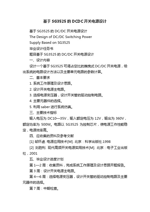
VT1和VT2分别由SG3525的输出端A和输出端B输出的正向驱动电流驱动。电阻R2和R3是限流电阻,是为了防止注入VT1和VT2的正向基极电流超出控制器所允许的输出电流。C1和C2是加速电容,起到加速VT1和VT2导通的作用。由于SG3525的输出驱动电路是低阻抗的,而功率MOSFET的输入阻抗很高,因此输出端A和输出端B与VT1和VT2栅极之间无须串接限流电阻和加速电容,就可以直接推动功率MOSFET
3.Sync(引脚3):振荡器外接同步信号输入端。该端接外部同步脉冲信号可实现与外电路同步。
4.OSC.Output(引脚4):振荡器输出端。
5.CT(引脚5):振荡器定时电容接入端。
6.RT〔引脚6〕:振荡器定时电阻接入端。
7.Discharge(引脚7):振荡器放电端。该端与引脚5之间外接一只放电电阻,构成放电回路。
6增加了PWM锁存器。为了使关断电路更可靠的工作,SG3525在其内部增加了PWM锁存器。PWM比拟器输出信号首先送至PWM锁存器,锁存器由关断电路置位,由振荡器输出时间脉冲复位。当关断电路工作时,即使过电流信号立即消失,锁存器也可以维持一个周期的关断控制,直到下一周期时钟信号使锁存器复位为止。同时,由于PWM锁存器对PWM比拟器的置位信号进展锁存,误差放大器上的噪声信号、振铃及其他信号在此过程中都被消除了。只有在下一个时钟周期才能重新复位,可靠性大大提高。
锁存器由关断电路置位,由振荡器输出时间脉冲复位
1.Inv.input(引脚1):误差放大器反向输入端。在闭环系统中,该引脚接反应信号。在开环系统中,该端与补偿信号输入端〔引脚9〕相连,可构成跟随器。
2.Noninv.input(引脚2):误差放大器同向输入端。在闭环系统和开环系统中,该端接给定信号。根据需要,在该端与补偿信号输入端〔引脚9〕之间接入不同类型的反应网络,可以构成比例、比例积分和积分等类型的调节器。
基于SG3525的DCDC开关电源设计
基于SG3525的DCDC开关电源设计基于SG3525的DC/DC开关电源设计The Design of DC/DC Switching PowerSupply Based on SG3525毕业设计任务书题目基于SG3525的DC/DC开关电源设计一、设计内容设计一个基于SG3525可调占空比的推挽式DC/DC开关电源,给出系统的电路设计方法以及主要单元电路的参数计算。
二、基本要求1. 系统工作原理及设计思路。
2. 设计开关电源主电路。
3. 选择电源变压器,设计开关管的驱动控制电路。
4. 主要元器件的选择。
5. 利用saber进行系统仿真。
三、主要技术指标输入电压为DC10—35V,输入额定电压为12V,输出为360V,额定功率为500W。
电路以SG3525为控制芯片,使电源工作性能稳定,电源效率高。
四、应收集的资料及参考文献[1] 邹怀虚. 电源应用技术[M]. 北京:科学出版社.1998[2] 刘胜利. 现代高频开关电源实用技术[M]. 北京:电子工业出版社,2001五、毕业设计进度计划第1—2周:收集资料,完成系统工作原理及设计思路开题报告。
第3周:设计开关电源主电路。
第4—6周:选择电源变压器,设计开关管的驱动控制电路及主要元器件的选择。
第7周:中期检查。
第8—11周:利用saber进行系统仿真。
第12—13周:论文审核定稿。
第14—15周:答辩。
毕业设计开题报告题目基于SG3525的DC/DC开关电源设计一、研究背景21世纪是信息化的时代,信息化的快速发展使得人们对于电子设备、产品的依赖性越来越大,而这些电子设备、产品都离不开电源。
开关电源相对于线性电源具有效率、体积、重量等方面的优势,尤其是高频开关电源正变得更轻,更小,效率更高,也更可靠,这使得高频开关电源成为了应用最广泛的电源。
从开关电源的组成来看,它主要由两部分组成:功率级和控制级。
功率级的主要任务是根据不同的应用场合及要求,选择不同的拓扑结构,同时兼顾半导体元件考虑设计成本;控制级的主要任务则是根据电路电信号选择合适的控制方式,目前的开关电源以PWM控制方式居多。
SG3525A的功能
SG3525A和SG3527A的内部结构框图如图1所示,两芯片的时序控制电路相同,仅输出结构不同,其中SG3525A适用于驱动N沟道MOS管,而SG3527A适用于驱动P沟道MOS管。
SG3525A的功能如下,①工作电压范围8.0~35V。
②基准电压5.1V±1%。
③输入欠电压锁定(8.0~7.5V)。
④锯齿波振荡频率(FOSC=1/[(0.7*RT+RD)*CT])范围0.1~400kHz,其中t1=0.67RTCT为定时电容充电时间,t2=1.3RDCT为定时电容放电时间,定时电容引脚的信号波形如图2(a)所示,线性上升和指数下降对应充放电过程,锯齿波波幅1.0~3.3V。
⑤放电过程产生时钟信号输出,信号波形如图2(b)所示。
内部时钟信号复位PWM锁存器,并锁定或非门,禁止脉冲输出,因此死区时间即为放电时间;时钟信号还驱动触发器,触发器输出控制或非门,形成推挽式输出,触发器输出波形如图2(c)和(d)所示。
外部时钟信号可用于多芯片级联应用时的同步信号,主芯片的时钟输出信号作为从芯片的同步输入。
⑥PWM脉冲宽度由“反馈PWM输入”引脚COM和软启动引脚SS中电平较低的一端控制,控制电平与电容器CT 上的锯齿波进行比较,当锯齿波电平高于控制电平时,比较器输出高电平置位PWM锁存器,锁住PWM,防止多重脉冲。
控制电平线性增加时,输出晶体管中的电流扇出管导通时间线性增加,PWM锁存器的输出波形如图2(e)所示。
⑦非欠压和关断状态下,时钟信号、触发器输出Q和PWM锁存器输出P均为低电平时,OUTA输出高电平,输出A和B为推挽式工作方式,拉/灌电流峰值为±400mA,输出波形如图2(f)和(g)所示。
⑧软启动端SS以50µA电流向外接电容充电,电容大小设定软启时间,达到50%占空比的时间为SS4SSC105T×≈秒,其中SSC以µF为单位。
⑨关断引脚SD的电压>0.7V时,软启动电容以150µA电流开始放电,CSS电位下降,限制输出脉冲宽度。
SG3525A

本文涉及的是光明工程中一个课题的具体技术问题。
该课题的基本原理是逆变器由直流蓄电池供电,用太阳能为蓄电池充电,然后逆变电源输出220V、50Hz的交流电供用户使用。
在研制过程中,有时随机出现烧毁大功率管的现象,本文对这一现象给出了解决方案。
图1 SG3525A驱动MOS功率管电路图图2 逆变器工作过程中波形图(a)图3 (A)逆变器缓启动(B)逆变器硬启动SG3525A和逆变电源本课题研发的逆变器使用的核心器件是SG3525A,以下分别简述其基本性能和工作过程。
SG3525A基本性能SG3525A PWM型开关电源集成控制器包括开关稳压所需的全部控制电路,设有欠压锁定电路和缓启动电路可提供精密度为5V±1%的基准电压。
其开关频率高达200KHz以上,适合于驱动N沟道MOS功率管。
本课题使用SG3525A产生50Hz的准正弦方波,为逆变器提供输出功率信号,去推动N沟道MOS功率管90N08,如图1所示。
逆变器工作过程当SG3525A被加电后(12V)会输出两列50Hz反向的方波,其幅度为9V。
这两路方波分别进入G1、G2、G3、G4所示的四条支路(图1),经各电路分别调整后输出,输出脉冲序列如图2(B)所示。
最终调制合成为A、B 两端输出的交流方波。
其波形见图2(A)。
该50Hz的序列方波由A、B两端进入电力变压器DT。
通过变压器升压后由逆变器电源输出220V、50Hz交流方波。
根据市场的不同需求生产出200W、600W、800W各个系列的逆变电源。
问题的出现与解决逆变器在额定负载条件下能够长期运行,但是当进行负载切换时或者当外电路有严重扰动时,偶尔会发生大功率管MOSFET90N08烧毁的现象。
现以800W逆变器进行剖析。
缓启动:如图3(A)所示状态,同时满负载加在逆变器输出上,然后启动逆变器使之运行,一切正常工作。
硬启动:如图3(B)所示状态,即加满负载后再闭合开关K1强行硬启动。
这时就偶尔有大功率场效应管短路烧毁的现象发生,经分析发现当G3推动的大功率管TV3尚未完全关断时,G4开启了对应的大功率管TV4,如果TV3和TV4同时开通就会造成短路现象。
SG3525A脉宽调制器控制电路

SG3525A 脉宽调制器控制电路一.简介SG3525A 系列脉宽调制器控制电路可以改进为各种类型的开关电源的控制性能和使用较少的外部零件。
在芯片上的5.1V 基准电压调定在±1%,误差放大器有一个输入共模电压范围。
它包括基准电压,这样就不需要外接的分压电阻器了。
一个到振荡器的同步输入可以使多个单元成为从电路或一个单元和外部系统时钟同步。
在CT 和放电脚之间用单个电阻器连接即可对死区时间进行大范围的编程。
在这些器件内部还有软起动电路,它只需要一个外部的定时电容器。
一只断路脚同时控制软起动电路和输出级。
只要用脉冲关断,通过PWM (脉宽调制)锁存器瞬时切断和具有较长关断命令的软起动再循环。
当VCC 低于标称值时欠电压锁定禁止输出和改变软起动电容器。
输出级是推挽式的可以提供超过200mA 的源和漏电流。
S G3525A 系列的N O R (或非)逻辑在断开状态时输出为低。
²工作范围为8.0V 到35V ²5.1V ±1.0%调定的基准电压 ²100Hz 到400K H z 振荡器频率 ²分立的振荡器同步脚二.SG3525A 内部结构和工作特性(1)基准电压调整器基准电压调整器是输出为5.1V ,50mA ,有短路电流保护的电压调整器。
它供电给所有内部电路,同时又可作为外部基准参考电压。
若输入电压低于6V 时,可把15、16脚短接,这时5V 电压调整器不起作用。
(2)振荡器3525A 的振荡器,除C T 、R T 端外,增加了放电7、同步端3。
RT 阻值决定了内部恒流值对CT 充电,CT 的放电则由5、7端之间外接的电阻值R D 决定。
把充电和放电回路分开,有利于通过R D 来调节死区的时间,因此是重大改进。
uc3525a(同SG3525)
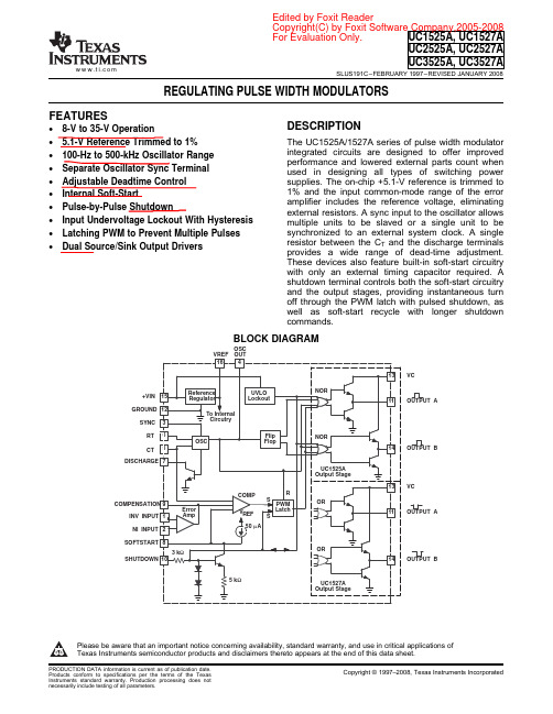
FEATURESDESCRIPTIONBLOCK DIAGRAMINV NI OUTPUT BOUTPUT AVCOUTPUT BOUTPUT A VCOSC UC1525A,UC1527A UC2525A,UC2527A UC3525A,UC3527ASLUS191C–FEBRUARY 1997–REVISED JANUARY 2008REGULATING PULSE WIDTH MODULATORS•8-V to 35-V Operation• 5.1-V Reference Trimmed to 1%The UC1525A/1527A series of pulse width modulator integrated circuits are designed to offer improved •100-Hz to 500-kHz Oscillator Range performance and lowered external parts count when •Separate Oscillator Sync Terminal used in designing all types of switching power •Adjustable Deadtime Control supplies.The on-chip +5.1-V reference is trimmed to 1%and the input common-mode range of the error •Internal Soft-Startamplifier includes the reference voltage,eliminating •Pulse-by-Pulse Shutdownexternal resistors.A sync input to the oscillator allows •Input Undervoltage Lockout With Hysteresis multiple units to be slaved or a single unit to be synchronized to an external system clock.A single •Latching PWM to Prevent Multiple Pulses resistor between the C T and the discharge terminals •Dual Source/Sink Output Driversprovides a wide range of dead-time adjustment.These devices also feature built-in soft-start circuitry with only an external timing capacitor required.A shutdown terminal controls both the soft-start circuitry and the output stages,providing instantaneous turn off through the PWM latch with pulsed shutdown,as well as soft-start recycle with longer shutdown commands.Please be aware that an important notice concerning availability,standard warranty,and use in critical applications of Texas Instruments semiconductor products and disclaimers thereto appears at the end of this data sheet.PRODUCTION DATA information is current as of publication date.Copyright ©1997–2008,Texas Instruments IncorporatedProducts conform to specifications per the terms of the Texas Edited by Foxit ReaderCopyright(C) by Foxit Software Company,2005-2008For Evaluation Only.RECOMMENDED OPERATING CONDITIONS (1)UC1525A,UC1527A UC2525A,UC2527A UC3525A,UC3527ASLUS191C–FEBRUARY 1997–REVISED JANUARY 2008These devices have limited built-in ESD protection.The leads should be shorted together or the device placed in conductive foam during storage or handling to prevent electrostatic damage to the MOS gates.These functions are also controlled by an undervoltage lockout which keeps the outputs off and the soft-start capacitor discharged for sub-normal input voltages.This lockout circuitry includes approximately 500mV of hysteresis for jitter-free operation.Another feature of these PWM circuits is a latch following the comparator.Once a PWM pulse has been terminated for any reason,the outputs will remain off for the duration of the period.The latch is reset with each clock pulse.The output stages are totem-pole designs capable of sourcing or sinking in excess of 200mA.The UC1525A output stage features NOR logic,giving a LOW output for an OFF state.The UC1527A utilizes OR logic which results in a HIGH output level when OFF.UCx52xAUNIT+V IN Supply voltage40V CCollector supply voltage 40VLogic inputs –0.3to +5.5Analog inputs–0.3to +V INOutput current,source or sink 500Reference output current 50mAOscillator charging current 5Power dissipation at T A =+25°C (2)1000mWPower dissipation at T C =+25°C (2)2000Operating junction temperature –55to 150Storage temperature range–65to 150°CLead temperature (soldering,10seconds)300(1)Values beyond which damage may occur.(2)See Thermal Characteristics table.(1)Range over which the device is functional and parameter limits are assured.2Submit Documentation Feedback Copyright ©1997–2008,Texas Instruments IncorporatedEdited by Foxit ReaderCopyright(C) by Foxit Software Company,2005-2008For Evaluation Only.THERMAL CHARACTERISTICSCONNECTION DIAGRAMS1234 5678161514131211109INV Input NI Input SYNC OSC OutputC T R TDischarge Soft StartV REF +V INOutput B V CGround Output A Shutdown CompensationJ or N PACKAGE (TOP VIEW)3212019910111213456781817161514Output B V C NC Ground Output ASYNC OSC OutputNC C T R TQ AND L PACKAGES(TOP VIEW)N I I n p u t I N V I n p u t N C C o m p e n s a t i o n S h u t d o w nV +V D i s c h a r g e S o f t S t a r t N C I NR E F NC − No internal connectionUC1525A,UC1527A UC2525A,UC2527A UC3525A,UC3527ASLUS191C–FEBRUARY 1997–REVISED JANUARY 2008over operating free-air temperature range (unless otherwise noted)PACKAGEθJA θJC J-1680-12028N-169045DW-1645-9025PLCC-2043-7534LCC-2070-8020PLCC-20,LCC-20DIL-16Copyright ©1997–2008,Texas Instruments Incorporated Submit Documentation Feedback3Edited by Foxit ReaderCopyright(C) by Foxit Software Company,2005-2008For Evaluation Only.ELECTRICAL CHARACTERISTICSf +1C T ǒ0.7R T )3RD ǓUC1525A,UC1527A UC2525A,UC2527A UC3525A,UC3527ASLUS191C–FEBRUARY 1997–REVISED JANUARY 2008+V IN =20V,and over operating temperature,unless otherwise specified,T A =T JPARAMETERTEST CONDITIONSMIN TYP MAX UNITREFERENCE UC152xA,UC252xA5.05 5.10 5.15Output voltage T J =25°C VUC352xA5.05.1 5.2Line regulationg V IN =8V to 35V 1020Load regulationg I L =0mA to 20mA 2050mVTemperature stability(1)Over operating range 2050UC152xA,UC252xA5.0 5.2Total output variation (1)Line,load,and temperature V UC352xA4.955.25Shorter circuit current V REF =0,T J =25°C 80100mA Output noise Voltage (1)10Hz ≤10kHz,T J =25°C 40200µVrms Long term stability (1)T J =125°C 2050mVOSCILLATOR SECTION (2)Initial accuracy (1)(2)T J =25°C 2%6%UC152xA,UC252xA0.3%1%Voltage stability (1)(2)V IN =8V to 35V UC352xA1%2%Temperature stability (1)Over operating range 3%6%Minimum frequency R T =200k Ω,C T =0.1µF 120Hz Maximum frequency R T =2k Ω,C T =470pF 400kHz Current mirror I RT =2mA1.72.0 2.2mA Clock amplitude (1)(2)3.0 3.5V Clock width (1)(2)T J =25°C0.30.5 1.0µs Syncronization threshold (1)(2)1.22.0 2.8V Sync input currentSync voltage =3.5V1.02.5mA ERROR AMPLIFIER SECTION (V CM =5.1V)UC152xA,UC252xA0.55mVInput offset voltage UC352xA210Input bias current 110µA Input offset current 1DC open loop gain R L ≥10M Ω6075dB Gain-bandwidth product (1)A V =0dB,T J =25°C12MHz DC transconductanc (1)(3)T J =25°C,30k Ω≤R L ≤1M Ω1.1 1.5mSLow-level output voltage 0.20.5V High-level output voltage 3.85.6Common mode rejection V CM =1.5V to 5.2V 6075dBSupply voltage rejection V IN =8V to 35V5060(1)These parameters,although ensured over the recommended operating conditions,are not 100%tested in production.(2)Tested at f OSC =40kHz (R T =3.6k Ω,C T =0.01µF,R D =0.Approximate oscillator frequency is defined by:(3)DC transconductance (g M )relates to DC open-loop voltage gain (A V )according to the following equation:A V =g M R L where R L is the resistance from pin 9to ground.The minimum g M specification is used to calculate minimum A V when the error amplifier output is loaded.4Submit Documentation Feedback Copyright ©1997–2008,Texas Instruments IncorporatedInv Input NI InputWCompto PWMComparatorUC1525A,UC1527A UC2525A,UC2527A UC3525A,UC3527ASLUS191C–FEBRUARY 1997–REVISED JANUARY 2008ELECTRICAL CHARACTERISTICS (continued)+V IN =20V,and over operating temperature,unless otherwise specified,T A =T JPARAMETERTEST CONDITIONSMINTYPMAXUNITPWM COMPARATOR Minimum duty-cycle 0%Maximum duty-cycle 45%49%Zero duty-cycle 0.70.9Input threshold (4)V Maximum duty-cycle3.3 3.6Input bias current (4)0.051.0µASHUTDOWN Soft-start current V SD =0V,V SS =0V 255080µA Soft-start low level V SD =2.5V0.40.7V Shutdown threshold To outputs,V SS =5.1V,T J =25°C 0.60.8 1.0Shutdown input current V SD =2.5V0.4 1.0mA Shutdown Delay (5)V SD =2.5V,T J =25°C 0.20.5µsOUTPUT DRIVERS (each output)(V C =20V)I SINK =20mA 0.20.4Low-level output voltage I SINK =100mA 1.0 2.0I SOURCE =20mA 1819V High-level output voltage I SOURCE =100mA 1718Undervoltage lockout V COMP and V SS =High 678V C OFF Current (6)V C =35V200µA Rise Time (5)C L =1nF,T J =25°C 100600nsFall Time(5)C L =1nF,T J =25°C 50300TOTAL STANDBY CURRENT Supply Current V IN =35V1420mA(4)Tested at f OSC =40kHz (R T =3.6k Ω,C T =0.01µF,R D =0Ω.(5)These parameters,although ensured over the recommended operating conditions,are not 100%tested in production.(6)Collector off-state quiescent current measured at pin 13with outputs low for UC1525A and high for UC1527A.UC1525A Error AmplifierCopyright ©1997–2008,Texas Instruments Incorporated Submit Documentation Feedback 5PRINCIPLES OF OPERATION AND TYPICAL CHARACTERISTICSClockF/F PWMOutput+V SUPPLYReturnUC1525A,UC1527A UC2525A,UC2527A UC3525A,UC3527ASLUS191C–FEBRUARY 1997–REVISED JANUARY 2008Figure 1.UC1525A Output Circuit (1/2circuit shown)Figure 2.Grounded Driver Outputs For Single-Ended SuppliesFor single-ended supplies,the driver outputs are grounded.The V C termainal is switched to ground by the totem-pole source transistors on alternate oscillator cycles.6Submit Documentation Feedback Copyright ©1997–2008,Texas Instruments IncorporatedReturnS a t u r a t i o n V o l t a g e − VOutput Current, Source or Sink − A+V SUPPLYReturnUC1525A,UC1527A UC2525A,UC2527A UC3525A,UC3527ASLUS191C–FEBRUARY 1997–REVISED JANUARY 2008PRINCIPLES OF OPERATION AND TYPICAL CHARACTERISTICS (continued)Figure 3.Output Drivers With Low Source ImpedanceThe low source impedance of the output drivers provides rapid charging of power FET input capacitance while minimizing external components.Figure 4.UC1525A Output Saturation Characteristics.Figure 5.Conventional Push-Pull Bipolar DesignIn conventional push-pull bipolar designs,forward base drive is controlled by R1–R3.Rapid turn-off times for the power devices are achieved with speed-up capacitors C1and C2.Copyright ©1997–2008,Texas Instruments IncorporatedSubmit Documentation Feedback 7+V SUPPLYReturnV REF R T C TWSYNCDISCHARGEGND UC1525A,UC1527A UC2525A,UC2527A UC3525A,UC3527ASLUS191C–FEBRUARY 1997–REVISED JANUARY 2008PRINCIPLES OF OPERATION AND TYPICAL CHARACTERISTICS (continued)Figure 6.Low Power TransformersLow power transformers can be driven by the UC1525A.Automatic reset occurs during dead time,when both ends of the primary winding are switched to ground.Figure 7.UC1525A Oscillator Schematic8Submit Documentation Feedback Copyright ©1997–2008,Texas Instruments IncorporatedShutdown Options (See Block Diagram)− T i m i n g R e s i s t a n c e − k R T ΩCharge Time − m s− D e a d T i m e R e s i s t a nc e −R D ΩCharge Time − m sMinimum Recommended R T − k WM a x i m u m r e c o m m e n d e d RDf − Frequency − HzO p e n -L o o p V o l t a g e G a i n − d B°°°O p e n -L o o p P h a s eUC1525A,UC1527A UC2525A,UC2527A UC3525A,UC3527ASLUS191C–FEBRUARY 1997–REVISED JANUARY 2008PRINCIPLES OF OPERATION AND TYPICAL CHARACTERISTICS (continued)Since both the compensation and soft-start terminals (Pins 9and 8)have current source pull-ups,either can readily accept a pull-down signal which only has to sink a maximum of 100A to turn off the outputs.This is subject to the added requirement of discharging whatever external capacitance may be attached to these pins.An alternate approach is the use of the shutdown circuitry of Pin 10which has been improved to enhance the available shutdown options.Activating this circuit by applying a positive signal on Pin 10performs two functions;the PWM latch is immediately set providing the fastest turn-off signal to the outputs;and a 150-A current sink begins to discharge the external soft-start capacitor.If the shutdown command is short,the PWM signal is terminated without significant discharge of the soft-start capacitor,thus,allowing,for example,a convenient implementation of pulse-by-pulse current limiting.Holding Pin 10high for a longer duration,however,will ultimately discharge this external capacitor,recycling slow turn-on upon release.Pin 10should not be left floating as noise pickup could conceivably interrupt normal operation.All transitions of the voltage on pin 10should be within the time frame of one clock cycle and not repeated at a frequency higher than 10clock cycles.Oscillator Charge Time vs R T and C TOscillator Discharge Time vs R T C TFigure 8.Figure 9.Maximum Value R D vs Minimum Value R TError Amplifier Voltage Gain and Phase vs FrequencyFigure 10.Figure 11.Copyright ©1997–2008,Texas Instruments Incorporated Submit Documentation Feedback9REFUC1525A,UC1527A UC2525A,UC2527A UC3525A,UC3527ASLUS191C–FEBRUARY 1997–REVISED JANUARY 2008PRINCIPLES OF OPERATION AND TYPICAL CHARACTERISTICS (continued)Figure b Test Fixture10Submit Documentation Feedback Copyright ©1997–2008,Texas Instruments IncorporatedTAPE AND REEL INFORMATION*All dimensions are nominalDevicePackage Type Package Drawing Pins SPQReel Diameter (mm)Reel Width W1(mm)A0(mm)B0(mm)K0(mm)P1(mm)W (mm)Pin1Quadrant UC2525ADWTR SOIC DW 162000330.016.410.8510.8 2.712.016.0Q1UC3525ADWTRSOICDW162000330.016.410.8510.82.712.016.0Q1*All dimensions are nominalDevice Package Type Package Drawing Pins SPQ Length(mm)Width(mm)Height(mm) UC2525ADWTR SOIC DW162000346.0346.033.0 UC3525ADWTR SOIC DW162000346.0346.033.0IMPORTANT NOTICETexas Instruments Incorporated and its subsidiaries(TI)reserve the right to make corrections,modifications,enhancements,improvements, and other changes to its products and services at any time and to discontinue any product or service without notice.Customers should obtain the latest relevant information before placing orders and should verify that such information is current and complete.All products are sold subject to TI’s terms and conditions of sale supplied at the time of order acknowledgment.TI warrants performance of its hardware products to the specifications applicable at the time of sale in accordance with TI’s standard warranty.Testing and other quality control techniques are used to the extent TI deems necessary to support this warranty.Except where mandated by government requirements,testing of all parameters of each product is not necessarily performed.TI assumes no liability for applications assistance or customer product design.Customers are responsible for their products and applications using TI components.To minimize the risks associated with customer products and applications,customers should provide adequate design and operating safeguards.TI does not warrant or represent that any license,either express or implied,is granted under any TI patent right,copyright,mask work right, or other TI intellectual property right relating to any combination,machine,or process in which TI products or services are rmation published by TI regarding third-party products or services does not constitute a license from TI to use such products or services or a warranty or endorsement e of such information may require a license from a third party under the patents or other intellectual property of the third party,or a license from TI under the patents or other intellectual property of TI.Reproduction of TI information in TI data books or data sheets is permissible only if reproduction is without alteration and is accompanied by all associated warranties,conditions,limitations,and notices.Reproduction of this information with alteration is an unfair and deceptive business practice.TI is not responsible or liable for such altered rmation of third parties may be subject to additional restrictions.Resale of TI products or services with statements different from or beyond the parameters stated by TI for that product or service voids all express and any implied warranties for the associated TI product or service and is an unfair and deceptive business practice.TI is not responsible or liable for any such statements.TI products are not authorized for use in safety-critical applications(such as life support)where a failure of the TI product would reasonably be expected to cause severe personal injury or death,unless officers of the parties have executed an agreement specifically governing such use.Buyers represent that they have all necessary expertise in the safety and regulatory ramifications of their applications,and acknowledge and agree that they are solely responsible for all legal,regulatory and safety-related requirements concerning their products and any use of TI products in such safety-critical applications,notwithstanding any applications-related information or support that may be provided by TI.Further,Buyers must fully indemnify TI and its representatives against any damages arising out of the use of TI products in such safety-critical applications.TI products are neither designed nor intended for use in military/aerospace applications or environments unless the TI products are specifically designated by TI as military-grade or"enhanced plastic."Only products designated by TI as military-grade meet military specifications.Buyers acknowledge and agree that any such use of TI products which TI has not designated as military-grade is solely at the Buyer's risk,and that they are solely responsible for compliance with all legal and regulatory requirements in connection with such use. TI products are neither designed nor intended for use in automotive applications or environments unless the specific TI products are designated by TI as compliant with ISO/TS16949requirements.Buyers acknowledge and agree that,if they use any non-designated products in automotive applications,TI will not be responsible for any failure to meet such requirements.Following are URLs where you can obtain information on other Texas Instruments products and application solutions:Products ApplicationsAmplifiers AudioData Converters AutomotiveDSP BroadbandClocks and Timers Digital ControlInterface MedicalLogic MilitaryPower Mgmt Optical NetworkingMicrocontrollers SecurityRFID TelephonyRF/IF and ZigBee®Solutions Video&ImagingWirelessMailing Address:Texas Instruments,Post Office Box655303,Dallas,Texas75265Copyright©2008,Texas Instruments Incorporated。
基于SG3525的单相正弦波并网逆变电源设计-PPT精品文档11页

该研究对逆变电路的全过程进行控制和检测,太阳能电池用 一个稳压电源和一个电阻串联的形式来模拟,具有最大功率 点跟踪(MPPT)功能,太阳能电池模拟电路输出电流恒定 在1A;电源输出电压频率自动跟踪电网电压频率,相对偏差 不大于1%;DC-AC变换器的效率 ≥60%;输出电压Uo的失 真度THD≤5%;具有欠压,过流等保护功能。
基于SG3525的单相正弦波并网 逆变电源设计
班 级:
作 者: 指导老师:
电子信息工程 2019级01班
肖宏忠 邵建设
目录
研究的目的、意义 研究内容 研究具体方法路线 研究结论
研究目的意义
随着全球工业化进程的逐步展开,世界各国对能源的需求 急剧膨胀,而煤炭、石油和天然气三大化石能源日渐枯 竭 ,人类迫不及待的探索新的能源,由于太阳能资源分布 相对广泛、蕴藏丰富,光伏发电系统具有清洁、安全、寿 命长以及维护量小等诸多优点,光伏发电被认为将是21世 纪最重要、最具活力的新能源 。
输出电压波形和相位跟踪波形
50Hz时
相位跟踪 波形
相位偏差 小于≤5°
45Hz时
频率跟踪波形
55Hz时
谢谢!
谢谢!--ຫໍສະໝຸດ DC- ACio1
io
T
滤
n1 n2
波 器
uo1
uo RL
n3
uREF 控制电路
uF
返回
主电路原理图
SPWM信号 产生电路
DC-AC 驱动电路
滤波 电路
DC-AC逆 变电返路回
欠压、过流 保护电路
控制电路原理图
基准信号产 生电路
频率跟踪 电路
取样电 路
基于SG3525的开关稳压电源设计

基于SG3525的开关稳压电源设计提出了一种采用PWM信号控制全控型电力电子器件的全桥开关稳压电源设计方法。
PWM专用芯片SG3525产生PWM方波,通过光电耦合隔离,经专用驱动芯片IR2110去驱动开关器件,达到开关稳压电源输出电压的稳定。
该电源具有输出电压稳定、电路简单、体积小、噪音小及可靠性高等特点。
标签:全桥电路,SG3525,PWM方波,驱动电路0 引言开关电源自20世纪90年代中期问世以来便显示出强大的生命力,它作为一项颇具发展前景和影响力的新产品,引起了国内外电源界的普遍关注。
开关电源具有高集成度、高性价比、最佳性能指标等特点[1-2],本文采用全桥电路拓扑设计并制作了额定输出功率为500W的开关稳压电源,具有输出电压从15V到25V 可调,纹波小的功能。
1 基本原理1.1系统组成开关电源按各部分的功能可分成:机箱、主电路、控制电路三部分[3]。
机箱既可起到固定的作用,也可起到屏蔽的作用。
主电路负责进行功率转换,通过适当的控制电路可以将市电转换为所需的直流输出电压。
控制电路则根据实际的需要产生主电路所需的控制脉冲和提供各种保护功能。
1.2 开关电源的基本工作原理PWM开关稳压电源的基本工作原理是在输入电压、内部参数以及外接负载变化的情况下,控制电路通过被控信号与基准信号的差值进行闭环反馈,调节主电路开关器件的导通脉冲宽度,使得开关电源的输出电压被控制信号稳定[4]。
对于单极性矩形脉冲来说,其直流平均电压取决于矩形脉冲的宽度,脉冲越宽,其直流平均电压值就越高。
直流平均电压由公式(1)计算:(1)式中—矩形脉冲最大电压值;—矩形脉冲周期;—矩形脉冲宽度。
当与不变时,直流平均电压将与脉冲宽度成正比。
这样,只要设法使脉冲宽度随稳压电源输出电压的增高而变窄,就可达到稳定电压的目的。
2主电路设计2.1 输入整流滤波回路本课题研究的电源额定工作状态的技术要求为:输出电压15V-25V,输出电流10A,输出功率为500W,属于中大功率电源。
- 1、下载文档前请自行甄别文档内容的完整性,平台不提供额外的编辑、内容补充、找答案等附加服务。
- 2、"仅部分预览"的文档,不可在线预览部分如存在完整性等问题,可反馈申请退款(可完整预览的文档不适用该条件!)。
- 3、如文档侵犯您的权益,请联系客服反馈,我们会尽快为您处理(人工客服工作时间:9:00-18:30)。
R3
SG3525
10
SD
C OMP
9
4K7
R7 100K R8
IN -
1
R9 4K7
IN +
2
C5 470/16V
1000u/35V C1
8
SS
V ref
16
RT
CT
GN D
C2
R11
10u/16V
3K6
DISC 7
6
5
12
R4
C3 R5
200
222 15K
图三:由TL494 组成降压型开关稳压电源
7
六 、 原 理 图
1A/400V
L1 10mH/0.5A
T1
TIP127 (100V/5A/Darl-L)
R1 4K7 R2
4K7
104 C4
4K7 104 R6 C4
FR107 D4
+12
5K1
104
R10
C6
VC C 1 5 13
VC OU TA
11 OU TB
14
7
O SC OU T
4K7
4. 易于建立工程设计概念:课题涉及多个典型的工程要素, 如:功率器件的最大电流、耐压、开关速度,磁性材料 的选择、功率电感的设计与绕制等。
5. 较典型的设计验证方法和负载实验。
3
三、单端正激式开关电源的工作原理
1. 导通状态 IONU LLt1UI LUOt1
2. 截止状态 IOFFULLt2 ULOt2
▪ 基准电压5.1V±1%
者取得控制权,脉宽正比于控制电平。 足,逐个脉冲的关断。
▪ 振荡频率0.1~400kHz ▪ SS端外接电容设定软启时间,达到 ▪ 输入欠电压锁定(施密特
▪ 充电时间~0.7RTCT
50%占空比TSS=5*104CSS
8.0~7.5V)
▪ 放电时间~3RDCT(死 ▪ 关断引脚电压>0.7V时,软启电容以 ▪ 锁住PWM防止多重脉冲。
6.8及相应十百千uF,耐压有6、16、25、
35、50、63、100、120、200、400V。
3. 工作频率:音频上限~50kHz, Fosc~41kHz,TOSC=24.4uS, tON=TOSCVO/(VIN-Vsta)=10.5~17.2uS。
1A/400V
L1 10mH/0.5A
T1
TIP127 (100V/5A/Darl-L)
R1 4K7 R2
4K7
104 C4
4K7 104 R6 C4
FR107 D4
+12
5K1
104
R10
C6
VC C 1 5 13
VC OU TA
11 OU TB
14
7
O SC OU T
4K7
3
/S YN C
IC1
3
/S YN C
IC1
R3
SG3525
10
SD
C OMP
9
4K7
R7 100K R8
IN -
1
R9 4K7
IN +
2
C5 470/16V
1000u/35V C1
8
SS
V ref
16
RT
CT
GN D
C2
R11
10u/16V
3K6
DISC 7
6
5
12
R4
C3 R5
200
222 15K
图三:由TL494 组成降压型开关稳压电源
VIN+VF
2. 滤波电容:RLC=(3~5)T,整流滤波后
IECO
VSTA
直流电压VIN=18.0~28.8V,
tON
tOFF
t
RL~18.0V/0.5A=36Ohm, T=10mS, 图四:开关管开关速度与功耗分析
1000uF/35V电解电容可满足要求。最
常用电解电容:1.0、2.2、3.3、4.7、
课程设计案例 分析
单端正激式开关稳压电源 或降压型开关稳压电源设计
1
一. 技术指标
1. 电源容量 ▪ 输入:交流15~24Vac。 ▪ 输出:电源电压+12V(不可调),纹波小于
50mVP-P,最大输出电流0.5A(限流型保护)。 2. 工作频率 ▪ 开关电源的工作频率为30~40kHz。 3. 控制电路 ▪ 采用脉冲宽度调制控制集成电路。
区时间)
150uA开始放电,进行限流;>1.4V时,▪ 双源/吸流输出±400mA
▪ 锯齿波1.0~3.3V
PWM锁存器关断输出。
5
五、SG3525A推荐的工作条件
条件 电源电压 集电极电压 输出吸入/源电流(待机) 输出吸入/源电流(峰值) 基准输出电流 计时电阻 计时电容 去磁电阻 振荡器频率 工作环境温度范围
3. 输入输出关系
IONIOFF
UO UI
t1 t1 t2
称为占空比
4
四、SG3525A、3527A的内部结构与功能
UCT
VCC
15
SG3525A的输出结构
Vref
16
基准调整器
欠压锁定
VC 13
OUTOSC
t
GND
12
或非
OUTA
11
OSCOUT
t
4
Q
SYNC
3
RT 6 RT
振荡器
触Iref RT CT RD Fosc TA
最小 8.0 4.5 0 0 0 2.0 0.001 0 0.1 0
最大 35 35 ±100 ±400 20 150 0.2 500 400 +70
单位 V V mA mA mA kΩ μF Ω kHz ℃
6
六 、 原 理 图
或非
OUTB
14
5 CT
Q
t
CT
DISC
/Q
7
RD
PWM比较器
SG3527A的输出结构
R
VC
COMP
S1
t
9
PWM
S2 锁存器 P
或非
OUTA
P
IN-
Vref
1
IN+
t
2
误差放大器
SS
50uA
8
或非
OUTB
OUTA
SD 5K
10
t OUTB
5K
t
▪ 工作电压8.0~35V ▪ 补偿COMP和软启动SS两端电平较低 ▪ 判断命令很短,放电不
2
二. 课题的意义
1. 具有实用性:几乎所有的电子设备都涉及电源设计,容 量较大时多采用开关电源。
2. 掌握一种共性技术:脉冲宽度调制技术-PWM是一项共 性技术,应用面广,如硅整流弧焊电源控制、逆变电源 设计、恒温控制、直流电机调速等。
3. 学习集成电路应用方法:TL494、SG3525A是常用的、 典型的固定频率的脉冲宽度调制控制电路,应用方法有 一定代表性。
软启动--上电时输出电压由低到高建立,需要一定时间。 上电时,C2充电需要一定时间,SS端电压由低逐渐变高,输出管的导 通时间逐渐增大,输出电压逐渐升高。
8
七、参数选择
IC VEC PT
1. 整流管:桥式整流,整流管电流=0.5负 载电流,最大反向电压=输入交流电压 峰值,IN4007(1A/1kV)可以满足要求。
▪ 稳压原理--输出电压负反馈。
若某种原因导致输出电压过高,则误差放大器1反向端电位升高,反馈/PWM端电
位降低,输出管导通时间减少,占空比减少,结果输出电压减少。最终使输出电
压保持稳定,R10和R11中点电压为5V。R7/R8为误差放大器的静态放大倍数,影
响控制精度。C4和R6影响误差放大器的动态放大倍数,抑制瞬变。