IC设计和版图中噪声减小的方法以及floorplan注意事项2
芯片制造中的电源噪声分析与抑制方法

芯片制造中的电源噪声分析与抑制方法在芯片制造过程中,电源噪声是一个十分重要的问题。
电源噪声可能会对芯片的性能和可靠性产生严重的负面影响。
因此,分析和抑制电源噪声成为了芯片设计中不可忽视的一环。
本文将详细探讨芯片制造中的电源噪声分析与抑制方法。
1. 电源噪声的来源在芯片制造过程中,电源噪声主要来自以下几个方面:1.1 电源本身的噪声:电源本身在工作时可能会产生一定的噪声,包括交流噪声和直流噪声。
这些噪声会通过电源引入到芯片中,对芯片的正常运行造成影响。
1.2 噪声耦合:芯片内部的各个模块之间,以及芯片与外部器件之间的电源噪声可能会相互耦合。
这种耦合可能导致一些模块之间的不稳定或互相干扰,进而影响芯片的整体性能。
1.3 临近线路的干扰:在芯片布局和设计中,不同模块之间的信号线可能会非常靠近,而且信号线之间可能会存在相互的电磁干扰。
这种干扰也可能会被引入到芯片的电源中,从而形成电源噪声。
2. 电源噪声的影响电源噪声对芯片的性能和可靠性具有重要的影响。
主要表现在以下几个方面:2.1 时钟抖动:电源噪声可能导致芯片时钟信号的抖动,进而影响芯片的时序准确性。
特别是对于高频时钟信号的抖动,可能会导致芯片的逻辑错误。
2.2 模拟信号干扰:电源噪声中的交流成分可能会传导到芯片的模拟信号中,导致模拟信号的准确性降低,影响芯片的模拟性能。
2.3 数字信号抖动:电源噪声可能导致数字信号的抖动,从而产生误码,降低芯片的通信速率和可靠性。
2.4 整体性能下降:电源噪声的存在可能会导致芯片整体性能的下降,包括功耗增加、工作温度升高等问题。
3. 电源噪声分析方法为了准确分析电源噪声,可以采用以下方法:3.1 频谱分析:通过对电源线上的信号进行频谱分析,可以确定电源噪声的频率分布情况。
这对于了解噪声产生的机制,以及选择合适的抑制方法具有重要意义。
3.2 非线性分析:电源噪声往往与芯片的非线性行为密切相关。
通过对芯片工作状态和电源噪声之间的关系进行分析,可以找到噪声的产生原因,进而采取相应的抑制策略。
消除PCB布局带来的噪声问题,这些要点要注意了

消除PCB布局带来的噪声问题,这些要点要注意了
提到“噪声问题”,往往让每个电子工程师都头痛不已,为了解决这个问题,经常要花费几个小时进行实验室测试,但最终却发现,噪声的元凶竟是
由开关电源的布局不当而引起的……
今天小编推荐一个ADI的所有电源器件评估板都采用的布局布线指导原则,以帮助大家避免此类噪声问题。
文中的示例开关调节器布局采用双通道同步
开关控制器ADP1850,第一步是确定调节器的电流路径。
然后,电流路径决定了器件在该低噪声布局布线设计中的位置。
一、确定电流路径
在开关转换器设计中,高电流路径和低电流路径彼此非常靠近。
交流(AC)
路径携带有尖峰和噪声,高直流(DC)路径会产生相当大的压降,低电流路径
往往对噪声很敏感。
适当PCB布局布线的关键在于确定关键路径,然后安排器件,并提供足够的铜面积以免高电流破坏低电流。
性能不佳的表现是接地
反弹和噪声注入IC及系统的其余部分。
图1所示为一个同步降压调节器设计,它包括一个开关控制器和以下外部
电源器件:高端开关、低端开关、电感、输入电容、输出电容和旁路电容。
图1中的箭头表示高开关电流流向。
必须小心放置这些电源器件,避免产生
不良的寄生电容和电感,导致过大噪声、过冲、响铃振荡和接地反弹。
图1. 典型开关调节器(显示交流和直流电流路径)
诸如DH、DL、BST和SW之类的开关电流路径离开控制器后需妥善安排,避免产生过大寄生电感。
这些线路承载的高δI/δt交流开关脉冲电流可能达到3A以上并持续数纳秒。
高电流环路必须很小,以尽可能降低输出响铃振荡,。
芯片设计中的布局与电源噪声耦合分析

芯片设计中的布局与电源噪声耦合分析芯片设计中的布局与电源噪声耦合分析对于确保电路的正常运行和性能稳定至关重要。
本文将对芯片设计中的布局技巧和电源噪声对芯片性能的影响进行深入探讨。
一、布局技巧对电源噪声的影响在芯片设计中,布局技巧是影响电源噪声的重要因素之一。
良好的布局可以有效地减小电源噪声的传播和耦合,提高电路的性能。
以下是一些常用的布局技巧:1. 电源电容的选择与布局:电源电容的选择直接影响到芯片的电源噪声性能。
合适的电源电容可以有效地降低电源噪声的传播和耦合。
同时,电源电容的布局也非常重要,应该尽量靠近芯片的电源引脚,减小电源回路的阻抗。
2. 地域划分和铺铜技术:合理划分芯片的地域,将模拟电路和数字电路区分开来,在布局时避免交叉干扰,从而降低电源噪声。
铺铜技术可以增加地域的铜层面积,减小阻抗,降低电源噪声的传播。
3. 时钟线的布局和分配:时钟线是芯片中非常重要的信号线,对时钟线的布局和分配要格外注意。
应尽量避免时钟线与其他信号线的交叉干扰,减小电源噪声的耦合效应。
二、电源噪声对芯片性能的影响电源噪声如果无法得到控制,会对芯片的性能造成严重的影响。
以下是一些电源噪声对芯片性能的可能影响:1. 时钟抖动:电源噪声会导致时钟信号的抖动,进而影响芯片的时序性能和稳定性。
时钟抖动会导致数据传输错误、时序失败等问题。
2. 敏感信号干扰:电源噪声可能会通过耦合或传导,干扰芯片中的敏感信号,导致系统的工作不稳定或性能下降。
3. 功耗增加:电源噪声会导致芯片电路的功耗增加,从而影响芯片的能效和工作稳定性。
三、布局与电源噪声耦合分析方法为了准确分析布局与电源噪声的耦合效应,可以采用以下方法:1. 仿真与分析:通过电磁仿真软件,对芯片的布局进行电源噪声仿真和分析。
通过仿真结果可以直观地看到电源噪声的分布和耦合情况,帮助进行布局调整和优化。
2. 实测与验证:通过实测来验证仿真结果的准确性,并进一步优化布局。
实测中可以采用专业的测量仪器和技术,对芯片的电源噪声进行定量分析。
IC设计和版图中噪声减小的方法以及floorplan注意事项2

IC设计和版图中噪声减⼩的⽅法以及floorplan注意事项2 Noise Reduction Is Crucial To Mixed-Signal ASIC Design Success (Part II)Floorplanning, I/O placement, pinout, and power-stability issues round out the noise-reduction design problem.by Jerry Twomey IBM MICROELECTRONICSLarge CMOS ASICs and system-on-a-chip designs often contain both analog and digital sections. Combining the two into a mixed-signal IC frequently leads to noise problems. This article, the second in a two-part series, deals with noise-reduction matters affecting the whole IC.As discussed in the first article, engineers should think about addressing noise issues as part of the design process to avoid such difficulties during chip debug ["Noise Reduction Is Crucial To Mixed-Signal ASIC Design Success (Part I)," electronic design, Oct. 30, p. 123]. Dealing with the trouble after the fact can be costly. Complicating the situation is the fact that Spice simulations often don't show many noise problems. Impedance of interconnects, adjacent device coupling, and substrate noise are usually not modeled accurately.Transition switching noise is an RF issue, with a very broad spectrum. At these frequencies, connection inductance and parasitic capacitance become significant factors.Noise coupling is often distributed, with multiple talkers and listeners. Most effective methods of noise reduction include suppression of talkers at the source and use of noise-immune listeners throughout the IC. For our purposes, "noise reduction" refers to both reducing noise sources and using circuits and layouts that make the system less sensitive to noise. Note that including noise immunity in a design doesn't mean larger chips. Done properly, the die area usually doesn't change.Noise-Reduction MethodsNoise-reduction methods can be categorized into four areas: providing low impedance and quiet connections for power, ground, and substrate; designing analog circuits that are less sensitive to noise; reducing or silencing any noise generators; and separating the talker-listeners using proximity separation, separation in frequency, or separation in time.The following is a summary of the previous article, which dealt with noise immunity of internal circuits.Differential circuits and signals provide common-mode noise rejection and less sensitivity to power and ground noise.Limiting circuit bandwidth helps to avoid noise amplification--using just enough bandwidth to get the job done. Wide-bandwidth circuits would amplify undesired system noise as well. Plus, RF filters on analog signals can cut down on parasitic coupling of noise.Reducing the number of external analog signals minimizes opportunities for noise coupling. Using large-amplitude signals directly improves the signal-to-noise ratio.Internally distributed power filtering placed in unused areas, under metal traces, and in similar locations can provide better power stability, especially at high frequencies.Extensive use of grounded substrate contacts, n-well tie-ups, and guard rings (well beyond what design rules require for latch-up protection) will reduce substrate noise.Signal separation and shielding helps to avoid noise coupling through parasitic capacitance. In addition, by using separated analog-digital routing and keeping talker-listener signals apart, noise concerns will improve.The most significant source of noise in most mixed-signal ASICs comes from digital transition switching. Strategies to decrease digital noise generation include minimum drive-strength devices, low-noise logic types, differential output drivers, and limited slew-rate devices.Some analog circuits produce noise due to transition switching. On/off current situations, current and voltage pulses, and any switched step voltages are the items to look for here. Removing these elements, or reducing their effects as a noise generator, will give better noise performance.Following these eight noise-immunity tips for an IC's internal circuits will go a long way toward creating a noise-robust system. Attention then turns to integrating these circuits onto an IC. This includes circuit placement, selection of I/O drivers, pin placements, interconnect issues, and power, ground, and substrate concerns.At high frequencies, the impedance associated with interconnect metal, bond wire, and the package's lead frame can become a significant factor in the stability of internal power/ground. For the digital section, maximizing the number of parallel power/ground pins to reduce impedance should be considered as a starting point.Separating the power/ground connections used for the analog sections from those used for the digital areas will improve the isolation of the power supplies. Analog cells that use large current transients (large di/dt) should be considered for independent power/ground interconnects. If possible, consider redesign of these circuits to a current-steering method to avoid current transients on the power supply.Fig. 1Separating the analog and digital power/groundconnections will improve isolation of the powersupplies. The configuration in (a) is usually themost problematic method for power stability. Asomewhat better layout is shown in (b). The circuitin (c) is the best because it provides no direct pathfor noise due to digital transition switching on theanalog circuit power.Figure 1 (above) illustrates the possible interconnect situations. The configuration in Figure 1a is usually the most problematic method for power stability. Any transition currents convert directly to noise on the analog power. This is due to interconnect impedance and the impedance of the package and bond wire. A somewhat better layout is represented by Figure 1b. This arrangement eliminates the internal interconnect impedance as part of the analog circuit's power-supply connection.Independent Connections Are BestThe optimal circuit is shown in Figure 1c. It provides no direct path for noise due to digital transition switching on the analog circuit power. Consider independent connections for any analog circuits that generate large current transients.Isolated power supplies are preferred for analog circuits. Yet even separated power supplies become somewhat noisy due to internal coupling. Consequently, some noise will still be present on all nodes, but the effects due to V = L(di/dt) will have been minimized.The RF nature of system noise indicates that the interconnect impedance and its filter capacitors need to be taken into account. External power filter capacitors will have a maximum frequency at which they function as a filter. High-frequency models for any capacitor include some series inductance. Capacitors exhibit self-resonance at higher frequencies. At these levels, the series inductance, which is internal to the capacitor, starts to dominate the impedance equation. Larger-value capacitors go through self-resonance at lower frequencies.Parallel filter capacitors of different values can provide more effective power filtering at higher frequencies. Placing the filter capacitors' resonance points in staggered locations will provide a flatter power-to-ground impedance. Also, to minimize inductance of the pc-board connection, external filters should be placed close to the IC.Fig. 2At high frequencies, package and bond-wireinductance reduces the effectiveness of anyexternal filter. This diagram shows a powernetwork that includes package/bond-wireimpedance and high-frequency models forexternal capacitors.At high frequencies, package and bond-wire inductance lessens the effectiveness of any external filter. Bond wires are typically 2 nH. In many cases, the package will increase the total inductance anywhere from 5 to 10 nH. Figure 2 (above) shows a network that includes package/bond-wire impedance and high-frequency models for external capacitors.Filter Capacitors NeededCapacitors on the die become necessary for high-frequency filtering. Internal capacitance doesn't have to be big. But it does have to be able to provide the filtering that the interconnect inductance won't allow to be placed externally. The presence of active circuits and interconnects means that there will already be some internal filtering between the power rails due to parasitic capacitance. Additional internal filters also can be used without increasing the size of the IC.As circuits are floorplanned into the IC, empty locations in the layout can be "filled" with filter capacitors. Stacking metal power and ground connections provides metal-plate capacitors. There are often large metal-only interconnect areas in an IC, and the layers underneath the metal can be used for internal power filtering. This method has been used to provide sizable internal filter capacitors without increasing the IC size.A combination of proper power-supply separation and external/internal filtering should give a stable, low-impedance, low-noise power and ground for analog circuits. Substrate areas will benefit from extensive tie-downs to ground, thereby providing less noise in these areas. In a similar fashion, n-well areas can use extensive tie-ups to the power supply. The prior article covered these topics in more detail.Internal circuits can have long interconnects used for signal routing between circuits. To diminish coupling, it's better to keep analog signal paths short. Digital and analog signals should be kept away from each other when possible. When it's necessary for these signals to be in close proximity, shielding should be implemented to reduce coupling.Fig. 3Digital and analog signals should be keptaway from each other if possible. Whenthese signals must be in close proximity,routing the digital lines under a shieldinglayer will reduce coupling (a). Shields canbe used to both isolate the listener andsuppress the talker (b).Shields limit noise coupling to signals within noisy environments (Fig. 3 above). They can be used both to isolate the listener and to suppress the talker. Therefore, the routing of digital signals near an analog circuit can be shielded as well. This minimizes the effects that noisy digital signals may have on analog circuits.To be most effective, shields of analog signals should be connected only at the noise-sensitive receiver. The intention is to keep the noise level low, as referenced to the susceptible device.Talker-listener separation is especially important in the I/O cells and in the package/bond-wire area at the perimeter of the IC. I/O cells develop large transient currents when driving external loads and become significant sources of noise. Lead-frame and bond-wire structures can have significant inductance and significant coupling to adjacent pins.When developing a strategy for pin placement, signal and control pins can usually be classified into several groups. Among them are sensitive analog signals, wide-swing analog signals, static/inactive digital controls, and clocks or active digital signals. Also, determine the necessary number of power and ground pins. As discussed in the section on power/ground stability, provide multiple parallel power and ground connections to reduce interconnect impedance. In addition, designate separate power and ground pins for analog and digital circuits, noise-sensitive analog circuits, and circuits that generate current transients. The goal is to keep transition noise away from any linear circuits.Once a total pin count is defined, pin placement for the chip perimeter can be selected. Some guidelines follow:Analog pins will have lower amounts of noise when widely separated from active digital pins. Putting the analog and digital circuits at opposite ends of the chip is a common strategy here.The highest-frequency digital pins are usually the greatest noise source and should be given widest separation from the analog sections.Analog pins can be isolated by the use of adjacent ground or "quiet" dc power pins.Static digital signals are low noise, which means they can be used for separation. This includes Chip Select or Chip Enable types of functions.Any high-frequency digital pins should be separated by static controls or power/ground pins. Doing so decreases cross-coupling effects between adjacent digital pins.These guidelines aid in defining the perimeter of the IC. Once the perimeter is established, the designer can then turn to the placement of circuits within the IC.As a general guideline, attempts should be made to avoid long interconnects on any analog signals. Any externally connected analog signals should have their internal circuits at close proximity to their I/O cell. With a careful selection for pinplacement, this area should not have any close-proximity digital drive I/O cells.Analog Cells Can Be Noisy TooSome analog cells can be noise generators as well. Therefore, they need to be examined on a case-specific basis. Be aware of transition switching, high voltage, or current transients. Also, these types of circuits shouldn't be placed near low-amplitude signals or high-gain/bandwidth analog circuits.Modern digital design includes HDL definition, synthesis, and a computer-controlled placement and routing system. Trying to invoke placement selection during that stage of design isn't frequently done. When in the floorplanning stage of the design, however, there's an additional noise-reduction technique available.Before routing, the digital system can be separated into two groups--static digital controls and dynamic, actively clocked, digital circuits. Static controls consist of items that are of a "set and forget" nature. Control registers that are downloaded once at circuit startup are a good example. Active digital systems consist of all circuits that are continually clocked while the IC is functioning.Constantly clocked digital circuitry is the dynamic noise generator, not static devices. The static logic is quiet and can be used as a separation tool between the analog circuits and the dynamic logic. Placing the active digital farthest away from the analog circuits and using the static digital as a space buffer between them improves separation without increasing the die size.Fig. 4Floorplanning helps prevent mixed-signalIC noise problems. Placing the active digitalcircuits farthest away from the analogcircuits, and using the static digital as aspace buffer between them, improvesseparation without increasing the die size.The right side of the IC layout has the mostnoise sources, while the left side has thefewest.In Figure 4 (above), active digital circuits and digital I/O cells are grouped to one side of the chip. The right side of the layout has the most noise sources, while the left side has the fewest. Substrate noise is "soaked up" by a guard-bar structure between active and static digital circuits.Static digital circuits are used as a separation tool between the analog and active digital sections. Substrate noise is further limited through use of an additional guard bar, which is set at the center of the IC. The center guard bars include two sets: one referenced to the digital power/ground, and the other referenced to the analog power/ground.Within the analog part of the chip, any large-amplitude analog circuits are placed toward the digital side. Small-amplitude analog circuits are given the spot with the widest separation from the digital I/O area.Physical separation between some analog cells may also be needed. Any analog circuits with voltage/current transientsshould be considered for separation and isolation from more sensitive circuits.I/O drivers, due to their sizeable external loads, generate substantial surge currents when switching. These drivers should use the lowest drive strength necessary to meet clock-rate and load requirements. If the rise and fall time is much shorter than the design needs, there will be more noise due to the high-drive strength capability of the I/O cell. Plus, faster rise times lead to higher-frequency noise and greater problems with parasitic capacitance and inductance of interconnects.High-voltage-swing off-chip drivers can often be eliminated in favor of reduced-swing outputs, differential voltage outputs, or current-steering differential outputs. Moreover, output drivers that use a controlled-voltage rise time will produce lower bandwidth noise and smaller current transients.In the final analysis, addressing the noise problem as part of the design process enables the designer to create functionalsilicon with less need for redesign. Most noise problems are not seen in simulations. Engineers need to be aware of this and make an effort to examine their circuits as both a potential "listener" or possible "talker." Doing so reduces noise issues.Floorplanning, I/O selection, and pin locations can all affect noise and coupling between circuits. Most noise-reduction strategies do not cause die-size increases if carefully done. Build as much noise immunity into the system as possible. Noise suppression, shielding, guard rings, internal/external filtering, talker-listener separation, and power/ground/substrate stability will all help improve performance.Trying to deal with noise problems after design and fabrication frequently leads to a set of redesign cycles--suppressing the greatest noise source, refabricating the IC, and then discovering the next biggest source of noise in the IC. Hopefully, this can be avoided.。
IC设计中常用的电路设计技巧与经验分享

IC设计中常用的电路设计技巧与经验分享电路设计是IC设计中不可或缺的一部分,它涉及到模拟电路、数字电路、射频电路等多个领域。
本文将从信号传输、降噪、时序设计等多个方面,分享一些常用的电路设计技巧与经验。
1. 信号传输方面在电路设计中,信号传输是一项非常重要的工作。
在信号传输过程中,信号存在着信号衰减、噪声干扰等问题。
如何在信号传输中保证信号质量呢?(1)阻抗匹配当信号源与接收器之间存在着阻抗不匹配时,会导致信号反射、信噪比下降等问题。
因此,在电路设计中要通过阻抗匹配来保证信号传输质量。
在实际设计中,可以通过调整电阻、电容等元器件的数值来实现阻抗匹配。
(2)信号放大和滤波在信号传输过程中,信号需要经过放大和滤波才能达到最终的目的。
放大电路可以将信号放大到足够的幅度,以确保信号可以被正常传输。
滤波则可以去除信号中的高频噪声和低频噪声,提高信号的可靠性和稳定性。
在实际设计中,要根据信号的特点选择合适的放大电路和滤波电路。
2. 降噪方面噪声是电路设计中不可避免的问题,它会干扰信号的传输和处理,降低系统的可靠性和性能。
如何在电路设计中降低噪声呢?(1)提高阻抗匹配度当电路中存在着阻抗不匹配时,会导致信号的反射和传输质量的下降,从而增加噪声。
因此,在电路设计中要通过阻抗匹配来尽量减小噪声。
(2)降低噪声来源在电路设计中,可以通过减少噪声来源来降低总噪声。
例如,可以通过选择更好的元器件、布线等方法来减少噪声来源,从而降低总噪声。
(3)加强屏蔽在电路设计中,可以通过加强屏蔽来阻止噪声的入侵。
例如,在高频电路中,可以采用金属屏蔽箱对电路进行屏蔽,以减小噪声的影响。
3. 时序设计方面时序设计是电路设计中非常重要的一部分。
时序设计可以影响电路的工作频率、工作稳定性等多个方面。
如何在时序设计中保证电路的性能呢?(1)Clock 树设计在数字电路中,时钟信号是驱动电路的核心信号。
时钟信号的传输需要考虑时钟的分配、时钟门控、时钟反相等问题。
芯片设计中的噪声与抗噪声技术

芯片设计中的噪声与抗噪声技术在芯片设计领域,噪声是一个不可忽视的问题。
噪声可以对芯片的性能和可靠性产生负面影响,因此开发抗噪声技术是非常重要的。
本文将探讨芯片设计中的噪声来源以及常用的抗噪声技术。
一、噪声的来源噪声是指电子系统中的随机信号,它可以从多个方面产生。
首先,来自电源的噪声是芯片设计中最主要的噪声来源之一。
电源供应的不稳定性会引发电压和电流的波动,导致额外的噪声。
其次,温度对芯片性能的影响也是一个重要的噪声来源。
温度变化会导致电子元件的参数变化,从而影响芯片的性能。
此外,器件和材料的内部运动也会引发噪声。
这些因素综合起来会导致芯片中噪声的产生和传播。
二、抗噪声技术为了降低噪声对芯片性能的影响,芯片设计人员广泛应用各种抗噪声技术。
下面将介绍几种常见的技术:1. 电源滤波技术电源滤波技术是一种常用的抗噪声方法。
通过使用电源滤波器,可以有效地降低由电源供应不稳定性引起的噪声。
电源滤波器可以去除电源信号中的高频噪声成分,以及电源干扰信号,从而提供稳定的电源供应。
2. 器件和材料优化通过对芯片的器件和材料进行优化,可以减少内部运动产生的噪声。
例如,在选择晶体管时,可以选择低噪声系数的器件,以减少噪声的影响。
另外,使用低噪声材料,如低噪声放大器和低噪声电阻,也可以有效降低噪声。
3. 降噪电路设计在芯片设计中,可以采用各种降噪电路来抵消噪声的影响。
例如,差分电路可以平衡信号与噪声,从而提高抗噪声能力。
此外,采用抗噪声放大器和抗噪声滤波器等电路也能有效降低噪声干扰。
4. 地线和屏蔽技术地线和屏蔽技术可以在芯片设计中用来降低外部环境产生的噪声。
通过合理设计地线布局和屏蔽结构,可以减少来自外部电磁场和射频干扰的噪声。
这些技术可以提高芯片的抗噪声能力,保证其正常运行。
五、结论噪声是芯片设计中必须面对的问题,但通过合适的抗噪声技术,可以有效降低噪声对芯片性能的影响。
电源滤波技术、器件和材料优化、降噪电路设计以及地线和屏蔽技术都是常用的抗噪声方法。
芯片设计中的电源噪声抑制与布局优化策略与技术

芯片设计中的电源噪声抑制与布局优化策略与技术在芯片设计中,电源噪声是一个常见而严重的问题。
电源噪声可以干扰信号传输,在高频应用中尤为突出。
为了提高芯片性能和可靠性,需要采取一系列的抑制电源噪声的策略与技术,同时对芯片布局进行优化。
本文将探讨芯片设计中的电源噪声抑制与布局优化策略与技术。
一、电源噪声的产生与影响电源噪声可以由电源回路中的各种因素产生,如电源线的阻抗、电容与电感元件的阻抗、电源开关器件的开关过程中的电流尖峰等。
这些因素导致电源回路中产生多种频率的噪声,传导至芯片中引起电源噪声。
电源噪声对芯片的影响主要体现在两个方面。
首先,电源噪声会直接影响芯片的工作稳定性和性能表现。
一旦噪声超过芯片所能承受的范围,可能导致芯片崩溃或者数据传输错误。
其次,电源噪声还会通过芯片的供电网络传播至其他部件,从而对整个系统的性能产生影响。
二、电源噪声抑制策略与技术1. 优化电源回路设计电源回路的设计是抑制电源噪声的首要步骤。
在设计电源回路时,应尽量减小电源回路中的电阻和电感,以减小噪声的产生。
另外,可以采用滤波电容和电感元件等被动元件来滤除噪声信号。
此外,还可以采用分离式的电源设计,将模拟电源和数字电源分离,以减小相互之间的干扰。
2. 优化供电网络设计供电网络设计是抑制电源噪声的重要手段之一。
可以采用多层供电网络设计来提高供电电源的稳定性。
同时,合理布局电源引脚和接地引脚,减小供电网络的阻抗,以提高供电电源的质量。
此外,还可以使用电源分布式电感器(PDN)来降低电源噪声。
3. 选择低噪声稳压器件选择低噪声的稳压器件对抑制电源噪声至关重要。
稳压器件应具备高阻抗、低噪声、低电压漂移等特点。
同时,应注意稳压器件的布局和降噪电容的选择,以最大程度地降低噪声信号的传播。
三、芯片布局优化策略与技术1. 分离模拟与数字区域模拟与数字电路之间的干扰是芯片布局中需要解决的一个问题。
为了降低电源噪声对模拟电路的干扰,应将模拟电路与数字电路分离,并合理布局。
PCB设计中降低开关噪声方法详述

PCB设计中降低开关噪声方法详述并没有很多方法可以快速地对它的值进行评估。
只有对封装和电源分配系统进行仔细的检查和详细的仿真才能得出一个较为合理结果。
因为影响SSN 的因素实在是太多了,所以不可能要求得到一个精确的答案,而且要评估的几何体都是自然的三维结构,很大程度上还取决于单个芯片的封装(或者连接器)和管脚分布。
由于这个问题的困难度,所以建议对SSN 的估算最好是通过仿真和测量的双重途径。
而对于这种噪声源的控制,也只能遵循一些通用的规则。
根据同步开关噪声的产生原因,我们可以从去耦电容的放置,驱动级,以及芯片封装等主要几个方面讨论如何在设计中减小SSN,并分别对其进行仿真比较。
在实际设计中,经常加去耦电容于PCB 和MCM 系统抑制同步开关噪声。
理论上若去耦电容足够大并靠近有源电路,则可消除SSN噪声,如图所示。
但电容本身和通孔、电源板都有寄生电感,如果所有的电感之和远大于实际电源总线的电感,则不管去耦电容多大,也没有去耦效果. 如两电感值相等,则即使加更大的电容,去耦效率也仅为一半或更低。
不同去耦电容下的同步开关噪声因此,为了有效地抑制同步开关噪声,倾向使用自激频率比较高、高Q 值的中等电容(约1~10nF)分布于整个模块(因为大表面封装电容(如≥100nF)通常寄生电感大)。
在电路设计中可通过在芯片内部加去耦电容(即在GNDINT与V DD INT之间加去耦电容)的办法减小SSN的作用,如图所示:去耦电容降噪声电路利用软件对SSN进行具体分析时,可以构建图电路模型结构进行Spice仿真。
驱动端的输出缓冲器的详细模型可以如图所示:输出缓冲器建模对一般模型进行具体仿真分析,将三条信号线其中一条为开关状态(高电平为3.3V,低电平0V),另外两条分别保持高电平和低电平,负载用25pF的电容模拟。
上图为仿真的结果,其中横坐标表示时间(单位;ns),纵坐标表示电压(单位:V):(a)为有状态切换的信号线负载端电压波形;(b)为片内驱动器获得的供电电压波形;(c)为保持低电平的驱动器负载端电压波形;(d)为保持高电平的驱动器负载端电压波形。
芯片制造中的电源噪声分析与抑制

芯片制造中的电源噪声分析与抑制芯片制造是当今科技领域的重要组成部分,而其中电源噪声的分析与抑制更是至关重要。
本文将探讨电源噪声对芯片制造的影响,并提供一些有效的方法来分析和抑制电源噪声。
一、电源噪声对芯片制造的影响电源噪声是指电源在供电过程中引入的一种电压或电流的异常波动。
这种波动会对芯片的正常运行产生严重的干扰,如信号失真、时钟抖动和系统误差等。
因此,电源噪声的分析与抑制对于确保芯片制造的质量和稳定性至关重要。
首先,电源噪声会导致芯片的工作电压不稳定,从而影响芯片正常工作的可靠性。
特别是对于高性能芯片而言,电压波动可能造成芯片在高频信号处理过程中产生失真,进而威胁到芯片的整体性能和功能。
其次,电源噪声还会对芯片的时钟信号产生干扰。
时钟信号的精准和稳定对于芯片的正常工作至关重要。
由于供电过程中的电源噪声,时钟信号会受到抖动,从而导致芯片内部的各个模块同步出现问题,进而影响芯片的整体性能。
最后,电源噪声还会对芯片的模拟信号和数字信号产生影响。
模拟信号的精确度和稳定性是芯片正常运行中最为关键的因素之一,而电源噪声会导致模拟信号的失真和误差增大。
此外,电源噪声也可能通过耦合作用进入芯片的数字信号线路,从而引起数字信号的抖动和误码率的增加。
二、电源噪声的分析方法针对电源噪声的分析需要采用一些专业的工具和方法。
下面介绍几种常用的电源噪声分析方法。
1. 电源噪声频谱分析法:通过使用频谱仪等仪器,对电源噪声的频谱进行测量和分析。
通过观察频谱图,可以确定哪些频率范围的电源噪声较大,从而有针对性地进行抑制。
2. 时域分析法:通过使用示波器等仪器,对电源波形进行观测和分析。
时域分析能够展示电源噪声的快速变化和瞬态特性,有助于找出电源噪声的源头和传播路径。
3. 差分和共模噪声分析法:通过测量输入和输出信号之间的差分和共模噪声,可以分析芯片中电源噪声的耦合和传播情况,进而采取有针对性的抑制手段。
三、电源噪声的抑制方法为了降低电源噪声对芯片制造的影响,可以采取一些有效的抑制方法。
芯片设计中的功率噪声分析与抑制技术

芯片设计中的功率噪声分析与抑制技术在现代电子设备中,芯片设计和制造是关键的环节之一。
芯片的性能与功耗息息相关,而功耗又会导致噪声产生。
因此,功率噪声分析与抑制技术在芯片设计中变得至关重要。
本文将探讨功率噪声分析的意义、其产生原因以及一些主要的抑制技术。
一、功率噪声分析的意义功率噪声是指芯片中由功耗引起的电压和电流波动。
这些噪声会干扰芯片的正常工作,并可能引起其他电子设备的干扰。
因此,对功率噪声进行准确的分析具有重要意义。
首先,功率噪声分析可以帮助工程师们确定芯片的功耗情况。
通过对功率噪声的测量和分析,可以了解芯片在不同工作状态下的功耗特点,为后续的优化工作提供参考。
其次,功率噪声分析可以帮助工程师们找出功率噪声的来源。
芯片中的功率噪声可能来自于多个方面,比如时钟信号、电源波动以及信号线之间的耦合等。
通过深入分析功率噪声的来源,可以有针对性地采取措施进行抑制。
最后,功率噪声分析可以帮助工程师们评估芯片的可靠性和稳定性。
功率噪声的存在可能导致芯片的温度升高,从而影响其寿命和性能。
通过对功率噪声进行分析,可以预测芯片在长期使用中可能出现的问题,并进行相应的优化设计。
二、功率噪声产生的原因功率噪声产生的原因多种多样,下面将介绍几种常见的原因:1. 功耗不均匀分布:芯片中不同电路模块的功耗分布可能不均匀,在不同工作状态下可能会导致功率噪声的产生。
2. 电源波动:电源的稳定性对芯片的功率噪声产生有很大影响。
电源的电压和电流波动可能会引起芯片中的功率噪声。
3. 时钟信号噪声:时钟信号的频率和幅值的波动也可能导致功率噪声的产生。
时钟信号在芯片中的传输可能会引起噪声,进而影响芯片的正常工作。
三、功率噪声的抑制技术为了抑制功率噪声,工程师们采取了一系列的技术手段。
下面将介绍几种常见的技术:1. 电源线的滤波:通过在芯片电源线上安装适当的滤波电路,可以减小电源波动,从而降低功率噪声的产生。
2. 时钟信号的优化设计:通过优化时钟信号的传输路径和布线规则,可以降低时钟信号的噪声,减小功率噪声的产生。
集成电路设计中的噪声分析与降噪
集成电路设计中的噪声分析与降噪随着集成电路的发展和应用不断扩大,噪声问题在集成电路设计中变得越来越重要。
噪声是指在电路中发生的任何随机性质的电信号,这种信号可以来自于电源、器件本身、环境等多种因素,它会导致电路的性能降低,从而影响电路的可靠性和稳定性。
在集成电路设计中,对噪声的分析和控制显得尤为重要,因为它能够保证电路的正常运作,提高电路的可靠性和性能。
噪声的来源主要包括两个方面,一是器件本身的噪声,二是来自于外部环境和电源的噪声。
器件本身的噪声来源十分广泛,常见的有电阻、二极管、晶体管、场效应管等。
这些器件中的噪声可以是热噪声、1/f噪声、射频噪声等。
而来自于外部环境和电源的噪声包括电磁辐射、磁场、热噪声、电源波动等。
这些噪声会对电路的正常运作产生不同程度的影响,特别是对精度要求比较高的电路,这些噪声必须控制在一定的范围内才能保证电路稳定和性能良好。
在集成电路设计中,噪声分析是重要的一项工作。
噪声分析主要涉及噪声源生成的机理和噪声的传输以及电路的噪声计算和分析。
在进行噪声分析时,需要熟悉它的统计性质,例如噪声的频谱密度、均方根电压、功率谱密度等,这些参数能提供给设计人员在进行电路设计时一个重要的参考,同时,通过噪声分析,设计人员还可以了解到电路中不同器件噪声存在的情况,从而可以选择合适的器件进行设计,在指导电路设计选择参数和优化设计时设置正确的噪声限制。
除了噪声分析外,针对电路中噪声问题的解决主要有两种途径:降噪和抗噪声措施。
降噪是指通过改善电路的环境条件或掉电路本身的设计,减少噪声产生或者噪声通过电路的传输,以达到降低电路中噪声的目的。
在降噪的方法中,有下面几种常用的方式:(1)提高信号的信噪比。
信噪比是指从信号中提取出有用信号的强度和噪音强度之间的比值,提高信噪比能有效地降低噪声的干扰。
在电路设计中,可以通过增大信号幅度、减小噪声幅度和提高信号频率等多种方式来提高信噪比。
(2)优化电路布局结构。
电路低噪声设计与处理技术

电路低噪声设计与处理技术电路的噪声问题一直是电子工程师在设计电路时需要重视和解决的难题之一。
不仅会影响信号传输的质量,还会降低电路的性能和稳定性。
因此,电路低噪声设计与处理技术的研究与应用具有重要意义。
本文将从低噪声设计的基本原则、低噪声放大器的设计以及噪声处理技术等方面进行探讨。
一、低噪声设计的基本原则在进行低噪声设计时,需要遵循以下几个基本原则:1.降低信号链路中的温度在电路的各个环节中,温度是噪声产生和放大的主要原因之一。
因此,采取措施降低信号链路中的温度是降低噪声的有效方法。
比如,选择低噪声器件、优化布局、增加散热装置等。
2.减小传输线的噪声传输线是电子系统中常见的信号传输通道,噪声在传输线上会被放大。
因此,对传输线进行合理的特性阻抗匹配、减小线路长度、降低信号的传输速率等方法可以有效地减小传输线的噪声。
3.降低功率噪声功率噪声是由电源等因素引起的,会进入电路并影响信号的质量。
为了降低功率噪声,可以采用滤波器、稳压器、隔离器等措施,确保电路供电的稳定性。
二、低噪声放大器的设计低噪声放大器是电路中常见的元件,其设计对整个电子系统的噪声水平有着重要影响。
以下是一些常见的低噪声放大器设计技术:1.前端电路选择在放大器的前端,选择低噪声的晶体管或场效应晶体管作为放大器的核心元件。
这些器件具有较低的噪声系数和较好的线性特性,适合应用于低噪声放大器的设计。
2.负反馈设计采用负反馈技术可以有效地降低放大器的噪声。
通过引入反馈电路,可以控制放大器的增益和稳定性,并将一部分噪声回馈至输入端,从而减小总体的噪声。
3.优化阻抗匹配阻抗匹配是低噪声放大器设计中重要的一环。
通过合理选择输入和输出端口的阻抗,可以最大程度地减小反射和传输线噪声。
三、噪声处理技术除了低噪声设计,噪声处理技术在电路设计中也是不可忽视的。
以下是一些常见的噪声处理技术:1.滤波器设计滤波器是用来滤除杂散噪声和带状噪声的重要元件。
根据不同的噪声特性,可以选择合适的滤波器类型和频率响应,达到滤除噪声的目的。
集成电路设计的低噪声与高精度

集成电路设计的低噪声与高精度集成电路(IC)设计是一个复杂且精细的过程,尤其是在低噪声和高精度方面。
随着科技的不断发展,集成电路在各个领域中的应用越来越广泛,如通信、医疗、航空航天等。
这些应用对集成电路的性能提出了更高的要求。
本文将详细探讨集成电路设计的低噪声与高精度。
1. 低噪声设计在集成电路设计中,低噪声是一个重要的性能指标。
噪声会影响电路的稳定性和准确性,从而影响整个系统的性能。
为了实现低噪声设计,需要从以下几个方面入手:1.1. 选用低噪声元件在设计过程中,应选用具有较低噪声特性的元件。
例如,在模拟电路中,选用低噪声放大器和运算放大器;在数字电路中,选用低功耗、低噪声的逻辑器件。
1.2. 优化电路布局电路布局对噪声有重要影响。
合理的布局可以降低电路间的干扰,从而降低噪声。
在布局时,应注意以下几点:•尽量缩短信号路径,减少信号传输过程中的噪声积累;•电源和地线应尽量粗,以降低电阻和电感;•数字和模拟电路应分开布局,以减小相互干扰;•高速信号和低速信号应分开布局,避免相互干扰。
1.3. 滤波设计滤波是降低噪声的有效手段。
在设计过程中,应根据系统的实际需求,采用合适的滤波器。
例如,在模拟电路中,可采用低通、高通、带通、带阻等滤波器;在数字电路中,可采用数字滤波器。
1.4. 降噪技术除了上述方法外,还可以采用一些降噪技术,如差分放大、噪声抵消、电容耦合等。
这些技术可以有效地降低噪声,提高电路的性能。
2. 高精度设计高精度是集成电路设计的另一个重要指标。
高精度设计可以保证电路在特定条件下具有较高的性能稳定性。
为实现高精度设计,需关注以下几个方面:2.1. 选用高精度元件在设计过程中,应选用高精度、低失真的元件。
这类元件具有较好的线性度和稳定性,有利于提高电路的精度。
2.2. 温度补偿温度对集成电路的性能有很大影响。
在设计时,应考虑温度补偿措施,以减小温度变化对电路性能的影响。
例如,采用温度补偿电路、选用温度特性较好的元件等。
消除电源芯片电感噪声的方法

消除电源芯片电感噪声的方法我折腾了好久消除电源芯片电感噪声的方法,总算找到点门道。
一开始我真的是瞎摸索,就像在黑暗里找东西似的。
我先想到的就是换电感,觉得是不是这个电感本身质量不行。
我就从市场上找了好几个不同牌子不同参数的电感来换。
结果呢,有的换了之后噪声是小了一点,但还是有,有的换了根本没什么变化,这把我给整懵了。
后来我就寻思着,会不会是周围电路的问题呢。
我就开始检查线路,看看有没有虚焊或者短路的地方。
检查线路可费了我好大的劲,得一点点看,就跟找蚂蚁洞似的。
我发现有一处线路的焊点有点松动,我心想这下可算是找到问题了。
赶紧把焊点重新焊好,满怀期待地通电试试,可是噪声还是有。
当时我那个心情啊,真的很沮丧。
然后我又从网上查了好多资料,有人说可能是电源芯片的工作频率和电感不太匹配的问题。
我就试着调整电源芯片的工作频率,这个操作还挺复杂的,我就小心翼翼地按照说明去做,就像走在钢丝上一样,生怕搞砸了。
但是很可惜,这个方法也没有完全消除噪声。
再后来,我在实验的过程中偶然发现,给电感加上一个小小的滤波电容,噪声有比较明显的降低。
这可给了我很大的希望。
我就找了不同容值的电容来试,经过不断地测试,总算找到了一个比较合适的电容值,能够把电感噪声降到比较低的程度。
不过我也不敢确定这就是最好的办法,但是目前对我来说是比较有效的。
我还试过往电感上涂一些屏蔽胶,这个屏蔽胶说是可以减少电磁干扰。
涂的时候就得注意别涂太多,不然可能会影响散热。
这个方法呢,感觉有一点点效果,但不是特别明显,只能算是个辅助的手段吧。
我觉得要是想消除电源芯片电感噪声,就得从多个方面去尝试,像我刚刚说的换电感、检查线路、调整工作频率还有加滤波电容这些方法,都可以去试试,说不定在你那里就有不一样的效果呢。
而且在操作的时候一定要有耐心,这个过程真的是很考验人的。
Floorplan注意事项
Floorplan注意事项Floorplan注意事项Floorplan的好坏直接决定了Design的成败,需要反复迭代找出最优三要素:Timing,Power, RoutableTiming:内部数据流向合理:横向对⽐出最佳⽅案,可根据No module情况使⽤最少量的module调整标准单元摆放density均匀合理,区域最好⼤⽚相连:设置module时注意TU,对Fence和Region注意 EU;过于密集可以设置区域density或者使⽤blockagePower:Block摆放井然有序,根据亲疏分布:使⽤ToolBox对Block与Module供电充分:power stripe摆好后检查微调⼀下它们的位置,followpin摆完不要随便移动,power plan后verify power via没有供电死⾓,贴边贴⾓摆放,⼤的Block之间channel要有与followpin正交的power stripe: power plan前后要仔细检查局部供电单元过多则增加Power Stripe,避免IR-drop太⼤:Power stripe通常是不规则和不均匀分布的Power rings保证均匀供电,可以避免Hot spot和EM等问题部分信号通过tie cell接到power上,提供ESD保护Routable:长条形Block尽量与最近电源线正交,否则会占⽤布线资源⾛线密度刚好达到congestion可以承受的上限:可以试探⼀下Block间的临界距离;Halo最⼩多少合适添加Blockage时要谨慎考虑:避免引起cut spacing,short等viols⼩的Block之间可以没有空间,设置Halo防⽌⼲扰:不要直接贴Block边靠着互连线很多的Block之间⼀般要留⼀些空间给std cell,因为跨过⼤的Block可能需要空间插buffer。
在原理图设计、PCB布线和调试中避免CCD板机的噪声
在原理图设计、PCB布线和调试中避免CCD板机的噪声
噪声是一个很头痛的问题。
在CCD板机设计中经常遇到。
结合我设计过程中的一些经验和大家讨论一下怎样预防图像中的噪声。
1.原理图设计
电源要解决好,34063的各项性能都不好,建议不要再用了;开关电源的肖特基二极管不要用SOD323封装的,还是要用电流大一点的,功率电感和电容都应该用大一些的。
SS-11(CXD3142R)可以考虑先用开关电源把12V转换5V,再用线性电源把5V转成3.3V,这样板机的整个功耗会大些,但是线性电源的纹波会小点。
各个芯片的电源滤波电容不能少,钽电容和瓷介电容都不能少。
2.PCB设计
敏感信号走线要尽量短,不要打过孔,以避免阻抗不连续的地方,不要把敏感信号夹在电源层和地层之间。
需要特别注意的几个信号,模拟信号有CCD的输出到AGC这一段,AGC的DRIVEOUT到DSP,DSP到视频放大到输出复合电视信号,数字信号主要有
H1,H2,RG这几个比较快。
还有一定要考虑板机的散热,温度太高会影响芯片性能和图像质量。
3.调试
电源电压一点要准,比如3.3V的电源,如果只有3.2V,图像质量会很差。
开关电源如果是可调的,调节电阻要用1%的,不然会影响电源电压的精度。
输出滤波的电感,如果额定电流太小,会有很大的压降。
软件也很重要,H1,H2,RG的时序会影响图像的信噪比。
PCB布线设计中降低噪声与电磁干扰经验总结

PCB布线设计中降低噪声与电磁干扰经验总结PCB布线设计中降低噪声与电磁干扰的一些经验。
(1)能用低速芯片就不用高速的,高速芯片用在关键地方。
(2)可用串一个电阻的办法,降低控制电路上下沿跳变速率。
(3)尽量为继电器等提供某种形式的阻尼。
(4)使用满足系统要求的最低频率时钟。
(5)时钟产生器尽量*近到用该时钟的器件。
石英晶体振荡器外壳要接地。
(6)用地线将时钟区圈起来,时钟线尽量短。
(7)I/O驱动电路尽量*近印刷板边,让其尽快离开印刷板。
对进入印制板的信号要加滤波,从高噪声区来的信号也要加滤波,同时用串终端电阻的办法,减小信号反射。
(8)MCD无用端要接高,或接地,或定义成输出端,集成电路上该接电源地的端都要接,不要悬空。
(9)闲置不用的门电路输入端不要悬空,闲置不用的运放正输入端接地,负输入端接输出端。
(10)印制板尽量使用45折线而不用90折线布线以减小高频信号对外的发射与耦合。
(11)印制板按频率和电流开关特性分区,噪声元件与非噪声元件要距离再远一些。
(12)单面板和双面板用单点接电源和单点接地、电源线、地线尽量粗,经济是能承受的话用多层板以减小电源,地的容生电感。
(13)时钟、总线、片选信号要远离I/O线和接插件。
(14)模拟电压输入线、参考电压端要尽量远离数字电路信号线,特别是时钟。
(15)对A/D类器件,数字部分与模拟部分宁可统一下也不要交*。
(16)时钟线垂直于I/O线比平行I/O线干扰小,时钟元件引脚远离I/O电缆。
(17)元件引脚尽量短,去耦电容引脚尽量短。
(18)关键的线要尽量粗,并在两边加上保护地。
高速线要短要直。
(19)对噪声敏感的线不要与大电流,高速开关线平行。
(20)石英晶体下面以及对噪声敏感的器件下面不要走线。
(21)弱信号电路,低频电路周围不要形成电流环路。
(22)任何信号都不要形成环路,如不可避免,让环路区尽量小。
(23)每个集成电路一个去耦电容。
每个电解电容边上都要加一个小的高频旁路电容。
噪声分析与抑制在集成电路圆片设计中的应用
噪声分析与抑制在集成电路圆片设计中的应用噪声分析与抑制在集成电路芯片设计中的应用在集成电路芯片设计中,噪声分析与抑制是至关重要的步骤。
噪声是指在电路中引入的随机干扰信号,可能会对电路的性能和可靠性产生负面影响,因此理解噪声的来源、特性和影响,并采取相应的抑制方法是确保电路设计质量的关键。
首先,噪声分析是电路设计中的重要环节。
通过对电路中噪声的分析,可以定量地评估电路的性能和可靠性。
噪声主要分为两种类型:1)内部噪声,来自电路内部元器件的热噪声、随机过程噪声等;2)外部噪声,来自环境中的干扰信号、电源干扰、耦合噪声等。
了解噪声的频谱分布、功率密度和影响因素,可以通过数学模型和仿真工具对其进行分析和评估。
其次,通过噪声抑制技术来降低噪声对电路性能的影响,提高电路的信噪比和抗干扰能力。
以下是几种常见的噪声抑制方法:1. 降低电路中的噪声源:对噪声源进行恰当的电路设计和优化,例如减小热噪声生成器的阻值、降低电压降噪声、减少交叉耦合噪声等。
通过选择低噪声元器件和优化电路结构,可以有效降低噪声源对电路的影响。
2. 电路隔离和屏蔽:通过电路隔离和屏蔽技术,可以减少噪声源与电路之间的耦合。
常用的隔离和屏蔽方法包括使用屏蔽罩、增加电源滤波器、降噪电容等。
通过有效的屏蔽和隔离措施,可以防止外部干扰信号进入电路,从而减少噪声对电路的影响。
3. 信号处理和滤波:通过信号处理和滤波技术,可以减弱或滤除噪声信号。
例如,使用低通滤波器可以去除高频噪声,使用差分信号处理可以减少共模噪声的影响。
根据电路的特点和需求,选择合适的滤波器和信号处理方法可以显著提高电路的信噪比。
4. 优化功耗与性能平衡:在电路设计中,通常存在功耗与性能之间的权衡。
过高的功耗可能会导致电路的工作温度升高,从而产生更多的热噪声。
因此,在电路设计中需要合理平衡功耗与性能,使电路在满足性能要求的同时,尽量降低功耗带来的噪声干扰。
除了上述的抑制方法,重视抗干扰能力和噪声容限的设计也是集成电路芯片设计中的重要考虑因素。
噪音消除法
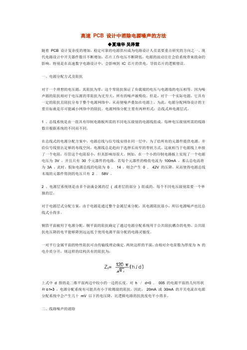
高速PCB 设计中消除电源噪声的方法◆夏瑞华吴泽慧随着PCB 设计复杂度的增加,稳定可靠的电源供应成为电路设计人员需要重点研究的方向之一。
现代电路设计中开关器件数目不断增加,芯片工作电压不断降低,电源的波动往往会给系统带来致命的影响,特别是在高速数字电路设计中,会影响到IC 芯片的供电,导致芯片的逻辑错误。
一、电源分配方式及阻抗对于一个理想的电压源,其阻抗为零,这个零阻抗保证了负载端的电压与电源端的电压相等。
因为噪声源的阻抗相对于电压源的零阻抗为无穷大,所有的噪声被吸收。
但是,对于一个实际电源,它具有一定的阻抗且阻抗分布于整个电源网络中,从而使噪声叠加在电源上。
为此,电源分配网络设计的主要目标就是尽可能减小网络中的阻抗。
电源网络分配主要有两种形式:总线式和电源层式。
1 、总线系统是由一组具有印制电路板所需的不同电压级别的电源线组成。
每种电压级别所需的线路数目根据系统的不同而不同。
在总线式的电源分配方案中,电源总线与信号线安排在同一层中,为了给所有的元器件提供电源,并给信号线留出足够的布线空间,电源线总是趋向于选择长而窄的带状方式。
这就相当于电源线上串接了一个电阻,尽管这个电阻很小,但其影响却很大。
例如,在一个小的印制电路板上实现了一个电源电压为3V ,并且只有30 个元器件的电路,若每个元器件的吸收电流为100mA ,那么总电流将为3A ,此时,假如电源总线的电阻为0 .14 ,则会产生0 .42V 的压降,从而使得电源总线末端的元器件得到的电压只有 2 .58V 。
2 、电源层系统则是由多个涂满金属的层( 或者层的部分) 组成的,每个不同电压级别需要一个单独的层。
对于电源层式分配方案,由于电源是通过整个金属层来分配,其电源阻抗很小,所以电源噪声也比总线式小得多。
铜箔平面被用于电源分配。
铜平面的阻抗确定了通过电源分配系统用于公共阻抗耦合的电势。
公共阻抗电压降的电平能够降到远远低于使用电源平面分配的电路灵敏度。
- 1、下载文档前请自行甄别文档内容的完整性,平台不提供额外的编辑、内容补充、找答案等附加服务。
- 2、"仅部分预览"的文档,不可在线预览部分如存在完整性等问题,可反馈申请退款(可完整预览的文档不适用该条件!)。
- 3、如文档侵犯您的权益,请联系客服反馈,我们会尽快为您处理(人工客服工作时间:9:00-18:30)。
Noise Reduction Is Crucial To Mixed-Signal ASIC Design Success (Part II)Floorplanning, I/O placement, pinout, and power-stability issues round out the noise-reduction design problem.by Jerry Twomey IBM MICROELECTRONICSLarge CMOS ASICs and system-on-a-chip designs often contain both analog and digital sections. Combining the two into a mixed-signal IC frequently leads to noise problems. This article, the second in a two-part series, deals with noise-reduction matters affecting the whole IC.As discussed in the first article, engineers should think about addressing noise issues as part of the design process to avoid such difficulties during chip debug ["Noise Reduction Is Crucial To Mixed-Signal ASIC Design Success (Part I)," electronic design, Oct. 30, p. 123]. Dealing with the trouble after the fact can be costly. Complicating the situation is the fact that Spice simulations often don't show many noise problems. Impedance of interconnects, adjacent device coupling, and substrate noise are usually not modeled accurately.Transition switching noise is an RF issue, with a very broad spectrum. At these frequencies, connection inductance and parasitic capacitance become significant factors.Noise coupling is often distributed, with multiple talkers and listeners. Most effective methods of noise reduction include suppression of talkers at the source and use of noise-immune listeners throughout the IC. For our purposes, "noise reduction" refers to both reducing noise sources and using circuits and layouts that make the system less sensitive to noise. Note that including noise immunity in a design doesn't mean larger chips. Done properly, the die area usually doesn't change.Noise-Reduction MethodsNoise-reduction methods can be categorized into four areas: providing low impedance and quiet connections for power, ground, and substrate; designing analog circuits that are less sensitive to noise; reducing or silencing any noise generators; and separating the talker-listeners using proximity separation, separation in frequency, or separation in time.The following is a summary of the previous article, which dealt with noise immunity of internal circuits.• Differential circuits and signals provide common-mode noise rejection and less sensitivity to power and ground noise.• Limiting circuit bandwidth helps to avoid noise amplification--using just enough bandwidth to get the job done. Wide-bandwidth circuits would amplify undesired system noise as well. Plus, RF filters on analog signals can cut down on parasitic coupling of noise.• Reducing the number of external analog signals minimizes opportunities for noise coupling. Using large-amplitude signals directly improves the signal-to-noise ratio.• Internally distributed power filtering placed in unused areas, under metal traces, and in similar locations can provide better power stability, especially at high frequencies.• Extensive use of grounded substrate contacts, n-well tie-ups, and guard rings (well beyond what design rules require for latch-up protection) will reduce substrate noise.• Signal separation and shielding helps to avoid noise coupling through parasitic capacitance. In addition, by using separated analog-digital routing and keeping talker-listener signals apart, noise concerns will improve.• The most significant source of noise in most mixed-signal ASICs comes from digital transition switching. Strategies to decrease digital noise generation include minimum drive-strength devices, low-noise logic types, differential output drivers, and limited slew-rate devices.• Some analog circuits produce noise due to transition switching. On/off current situations, current and voltage pulses, and any switched step voltages are the items to look for here. Removing these elements, or reducing their effects as a noise generator, will give better noise performance.Following these eight noise-immunity tips for an IC's internal circuits will go a long way toward creating a noise-robust system. Attention then turns to integrating these circuits onto an IC. This includes circuit placement, selection of I/O drivers, pin placements, interconnect issues, and power, ground, and substrate concerns.At high frequencies, the impedance associated with interconnect metal, bond wire, and the package's lead frame can become a significant factor in the stability of internal power/ground. For the digital section, maximizing the number of parallel power/ground pins to reduce impedance should be considered as a starting point.Separating the power/ground connections used for the analog sections from those used for the digital areas will improve the isolation of the power supplies. Analog cells that use large current transients (large di/dt) should be considered for independent power/ground interconnects. If possible, consider redesign of these circuits to a current-steering method to avoid current transients on the power supply.Fig. 1Separating the analog and digital power/groundconnections will improve isolation of the powersupplies. The configuration in (a) is usually themost problematic method for power stability. Asomewhat better layout is shown in (b). The circuitin (c) is the best because it provides no direct pathfor noise due to digital transition switching on theanalog circuit power.Figure 1 (above) illustrates the possible interconnect situations. The configuration in Figure 1a is usually the most problematic method for power stability. Any transition currents convert directly to noise on the analog power. This is due to interconnect impedance and the impedance of the package and bond wire. A somewhat better layout is represented by Figure 1b. This arrangement eliminates the internal interconnect impedance as part of the analog circuit's power-supply connection.Independent Connections Are BestThe optimal circuit is shown in Figure 1c. It provides no direct path for noise due to digital transition switching on the analog circuit power. Consider independent connections for any analog circuits that generate large current transients.Isolated power supplies are preferred for analog circuits. Yet even separated power supplies become somewhat noisy due to internal coupling. Consequently, some noise will still be present on all nodes, but the effects due to V = L(di/dt) will have been minimized.The RF nature of system noise indicates that the interconnect impedance and its filter capacitors need to be taken into account. External power filter capacitors will have a maximum frequency at which they function as a filter. High-frequency models for any capacitor include some series inductance. Capacitors exhibit self-resonance at higher frequencies. At these levels, the series inductance, which is internal to the capacitor, starts to dominate the impedance equation. Larger-value capacitors go through self-resonance at lower frequencies.Parallel filter capacitors of different values can provide more effective power filtering at higher frequencies. Placing the filter capacitors' resonance points in staggered locations will provide a flatter power-to-ground impedance. Also, to minimize inductance of the pc-board connection, external filters should be placed close to the IC.Fig. 2At high frequencies, package and bond-wireinductance reduces the effectiveness of anyexternal filter. This diagram shows a powernetwork that includes package/bond-wireimpedance and high-frequency models forexternal capacitors.At high frequencies, package and bond-wire inductance lessens the effectiveness of any external filter. Bond wires are typically 2 nH. In many cases, the package will increase the total inductance anywhere from 5 to 10 nH. Figure 2 (above) shows a network that includes package/bond-wire impedance and high-frequency models for external capacitors.Filter Capacitors NeededCapacitors on the die become necessary for high-frequency filtering. Internal capacitance doesn't have to be big. But it does have to be able to provide the filtering that the interconnect inductance won't allow to be placed externally. The presence of active circuits and interconnects means that there will already be some internal filtering between the power rails due to parasitic capacitance. Additional internal filters also can be used without increasing the size of the IC.As circuits are floorplanned into the IC, empty locations in the layout can be "filled" with filter capacitors. Stacking metal power and ground connections provides metal-plate capacitors. There are often large metal-only interconnect areas in an IC, and the layers underneath the metal can be used for internal power filtering. This method has been used to provide sizable internal filter capacitors without increasing the IC size.A combination of proper power-supply separation and external/internal filtering should give a stable, low-impedance, low-noise power and ground for analog circuits. Substrate areas will benefit from extensive tie-downs to ground, thereby providing less noise in these areas. In a similar fashion, n-well areas can use extensive tie-ups to the power supply. The prior article covered these topics in more detail.Internal circuits can have long interconnects used for signal routing between circuits. To diminish coupling, it's better to keep analog signal paths short. Digital and analog signals should be kept away from each other when possible. When it'snecessary for these signals to be in close proximity, shielding should be implemented to reduce coupling.Fig. 3Digital and analog signals should be keptaway from each other if possible. Whenthese signals must be in close proximity,routing the digital lines under a shieldinglayer will reduce coupling (a). Shields canbe used to both isolate the listener andsuppress the talker (b).Shields limit noise coupling to signals within noisy environments (Fig. 3 above). They can be used both to isolate the listener and to suppress the talker. Therefore, the routing of digital signals near an analog circuit can be shielded as well. This minimizes the effects that noisy digital signals may have on analog circuits.To be most effective, shields of analog signals should be connected only at the noise-sensitive receiver. The intention is to keep the noise level low, as referenced to the susceptible device.Talker-listener separation is especially important in the I/O cells and in the package/bond-wire area at the perimeter of the IC. I/O cells develop large transient currents when driving external loads and become significant sources of noise. Lead-frame and bond-wire structures can have significant inductance and significant coupling to adjacent pins.When developing a strategy for pin placement, signal and control pins can usually be classified into several groups. Among them are sensitive analog signals, wide-swing analog signals, static/inactive digital controls, and clocks or active digital signals. Also, determine the necessary number of power and ground pins. As discussed in the section on power/ground stability, provide multiple parallel power and ground connections to reduce interconnect impedance. In addition, designate separate power and ground pins for analog and digital circuits, noise-sensitive analog circuits, and circuits that generate current transients. The goal is to keep transition noise away from any linear circuits.Once a total pin count is defined, pin placement for the chip perimeter can be selected. Some guidelines follow:• Analog pins will have lower amounts of noise when widely separated from active digital pins. Putting the analog and digital circuits at opposite ends of the chip is a common strategy here.• The highest-frequency digital pins are usually the greatest noise source and should be given widest separation from the analog sections.• Analog pins can be isolated by the use of adjacent ground or "quiet" dc power pins.• Static digital signals are low noise, which means they can be used for separation. This includes Chip Select or Chip Enable types of functions.• Any high-frequency digital pins should be separated by static controls or power/ground pins. Doing so decreases cross-coupling effects between adjacent digital pins.These guidelines aid in defining the perimeter of the IC. Once the perimeter is established, the designer can then turn to the placement of circuits within the IC.As a general guideline, attempts should be made to avoid long interconnects on any analog signals. Any externally connected analog signals should have their internal circuits at close proximity to their I/O cell. With a careful selection for pin placement, this area should not have any close-proximity digital drive I/O cells.Analog Cells Can Be Noisy TooSome analog cells can be noise generators as well. Therefore, they need to be examined on a case-specific basis. Be aware of transition switching, high voltage, or current transients. Also, these types of circuits shouldn't be placed near low-amplitude signals or high-gain/bandwidth analog circuits.Modern digital design includes HDL definition, synthesis, and a computer-controlled placement and routing system. Trying to invoke placement selection during that stage of design isn't frequently done. When in the floorplanning stage of the design, however, there's an additional noise-reduction technique available.Before routing, the digital system can be separated into two groups--static digital controls and dynamic, actively clocked, digital circuits. Static controls consist of items that are of a "set and forget" nature. Control registers that are downloaded once at circuit startup are a good example. Active digital systems consist of all circuits that are continually clocked while the IC is functioning.Constantly clocked digital circuitry is the dynamic noise generator, not static devices. The static logic is quiet and can be used as a separation tool between the analog circuits and the dynamic logic. Placing the active digital farthest away from the analog circuits and using the static digital as a space buffer between them improves separation without increasing the die size.Fig. 4Floorplanning helps prevent mixed-signalIC noise problems. Placing the active digitalcircuits farthest away from the analogcircuits, and using the static digital as aspace buffer between them, improvesseparation without increasing the die size.The right side of the IC layout has the mostnoise sources, while the left side has thefewest.In Figure 4 (above), active digital circuits and digital I/O cells are grouped to one side of the chip. The right side of the layout has the most noise sources, while the left side has the fewest. Substrate noise is "soaked up" by a guard-bar structure between active and static digital circuits.Static digital circuits are used as a separation tool between the analog and active digital sections. Substrate noise is further limited through use of an additional guard bar, which is set at the center of the IC. The center guard bars include two sets: one referenced to the digital power/ground, and the other referenced to the analog power/ground.Within the analog part of the chip, any large-amplitude analog circuits are placed toward the digital side. Small-amplitude analog circuits are given the spot with the widest separation from the digital I/O area.Physical separation between some analog cells may also be needed. Any analog circuits with voltage/current transients should be considered for separation and isolation from more sensitive circuits.I/O drivers, due to their sizeable external loads, generate substantial surge currents when switching. These drivers should use the lowest drive strength necessary to meet clock-rate and load requirements. If the rise and fall time is much shorter than the design needs, there will be more noise due to the high-drive strength capability of the I/O cell. Plus, faster rise times lead to higher-frequency noise and greater problems with parasitic capacitance and inductance of interconnects.High-voltage-swing off-chip drivers can often be eliminated in favor of reduced-swing outputs, differential voltage outputs, or current-steering differential outputs. Moreover, output drivers that use a controlled-voltage rise time will produce lower bandwidth noise and smaller current transients.In the final analysis, addressing the noise problem as part of the design process enables the designer to create functionalsilicon with less need for redesign. Most noise problems are not seen in simulations. Engineers need to be aware of this and make an effort to examine their circuits as both a potential "listener" or possible "talker." Doing so reduces noise issues.Floorplanning, I/O selection, and pin locations can all affect noise and coupling between circuits. Most noise-reduction strategies do not cause die-size increases if carefully done. Build as much noise immunity into the system as possible. Noise suppression, shielding, guard rings, internal/external filtering, talker-listener separation, and power/ground/substrate stability will all help improve performance.Trying to deal with noise problems after design and fabrication frequently leads to a set of redesign cycles--suppressing the greatest noise source, refabricating the IC, and then discovering the next biggest source of noise in the IC. Hopefully, this can be avoided.。