LM1117-3.3 电压转换芯片 数据手册 说明书

- 1、下载文档前请自行甄别文档内容的完整性,平台不提供额外的编辑、内容补充、找答案等附加服务。
- 2、"仅部分预览"的文档,不可在线预览部分如存在完整性等问题,可反馈申请退款(可完整预览的文档不适用该条件!)。
- 3、如文档侵犯您的权益,请联系客服反馈,我们会尽快为您处理(人工客服工作时间:9:00-18:30)。
1A Low Dropout Positive Voltage Regulator
LM1117L3
Features Description
●
Adjustable or Fixed Output The LM1117 series of positive adjustable and fixed ●Output Current of 1A regulators are designed to provide 1A with high ●Low Dropout, 1.3V max at 1A Output Current efficiency. All internal circuitry is designed to ●0.04% Line Regulation operate down to 1.3V input to output differential. ●0.2% Load Regulation On-chip trimming adjusts the reference voltage to ●100% Thermal Limit Burn-in 1%.
●Fast Transient Response
Applications
●
High Efficiency Linear Regulators
● Post Regulators for Switching Supplies
● Adjustable Power Supply
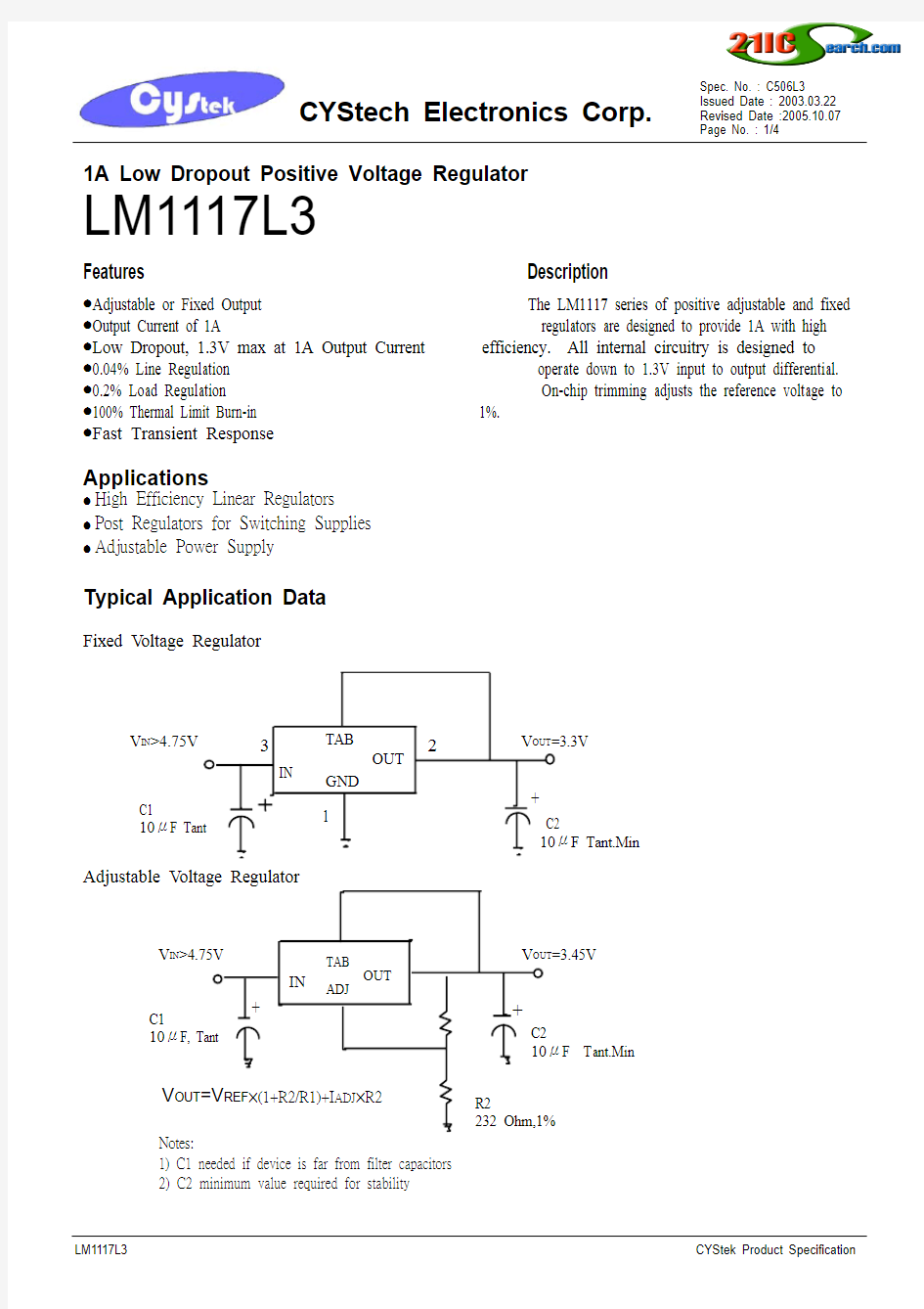
Typical Application Data
Fixed V oltage Regulator
Adjustable V oltage Regulator
V OUT =V REF ×(1+R2/R1)+I ADJ ×R2
1) C1 needed if device is far from filter capacitors
2) C2 minimum value required for stability
C2 10μF Tant.Min
V OUT =3.3V C1
10μF Tant V IN >4.75V 1 23IN TAB GND OUT +V OUT =3.45V C2 10μF Tant.Min R2 232 Ohm,1%
C1 10μF, Tant V IN >4.75V + IN TAB ADJ OUT
+
Package Information
SOT-223
Absolute Maximum Ratings
Symbol Parameter
Maximum Units PD Power Dissipation
Internally Limited W VIN Input Voltage
7 V TJ Operating Junction Temperature Range
Control Section
Power Transistor
0 to 125 0 to 150 ℃ TSTG Storage Temperature
-65 to 150 ℃ TLEAD Lead Temperature(Soldering, 10 sec) 300 ℃
Device Selection Guide
Device
Output Voltage LM1117-Adj
Adjustable LM1117-1.5
1.5V LM1117-1.8
1.8V LM1117-
2.5
2.5V LM1117-2.85
2.8 5V LM1117-
3.0
3. 0V LM1117-3.3
3.3V LM1117-3.5
3.5V LM1117-5.0
5.0V
Electrical Characteristics @I LOAD =0mA,T J =25℃, unless otherwise specified
Parameter Device
Test Conditions Min Typ Max Units V IN =5V,I LOAD =10mA 1.238 1.250 1.262Reference voltage
(Note 1) Adj Version
V IN =2.65V to 7V,I LOAD =10mA to 1A * 1.225 1.250 1.275V V IN =V OUT +1.5V
Variator from nominal V OUT
-1 +1 % V IN =V OUT +1.5V to 7V
I LOAD =0mA to 1A
Output Voltage (Note 1) Al fixed
version Variator from nominal V OUT * -2 +2 %
Line Regulation (Note 1) All I LOAD =10mA,(V OUT +1.5V)≦V ≦7V * 0.040.2Load Regualtion (Note 1) All V IN =V OUT +1.5V, I LOAD =10mA to 1A * 0.2 0.4
%
Minimum Load Current Adj Version V IN =5V,V ADJ =0V * 3 7mA
Ground Pin Current All fixed version V IN =V OUT +1.5V,I LOAD =10mA to 1A *713mA
Adjust Pin Current
Adj Version V IN =2.65V to 7V, I LOAD =10mA * 55 90µA Pin Function
1 ADJ/GND
2 OUTPUT
3 INPUT 1 2 3
