09_Block Diagram
Exercises1 (6)
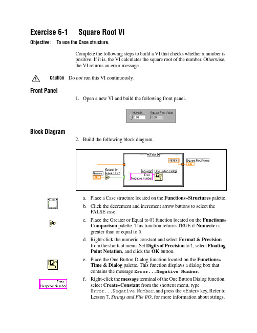
Exercise6-1Square Root VIObjective:To use the Case structure.Complete the following steps to build a VI that checks whether a number ispositive.If it is,the VI calculates the square root of the number.Otherwise,the VI returns an error message.Caution Do not run this VI continuously.Front Panel1.Open a new VI and build the following front panel.Block Diagram2.Build the following block diagram.a.Place a Case structure located on the Functions»Structures palette.b.Click the decrement and increment arrow buttons to select theFALSE case.c.Place the Greater or Equal to0?function located on the Functions»Comparison palette.This function returns TRUE if Numeric isgreater than or equal to0.d.Right-click the numeric constant and select Format&Precisionfrom the shortcut menu.Set Digits of Precision to1,select FloatingPoint Notation,and click the OK button.e.Place the One Button Dialog function located on the Functions»Time&Dialog palette.This function displays a dialog box thatcontains the message Error...Negative Number.f.Right-click the message terminal of the One Button Dialog function,select Create»Constant from the shortcut menu,typeError...Negative Number,and press the<Enter>key.Refer toLesson7,Strings and File I/O,for more information about strings.g.Select the TRUE case and place the Square Root function located onthe Functions»Numeric palette,as shown in the following blockdiagram.This function returns the square root of Numeric.3.Save the VI as Square Root.vi.4.Display the front panel and run the VI.If Numeric is positive,the VI executes the TRUE case and returnsthe square root of Numeric.If Numeric is negative,the VI executes the FALSE case,returns–99999.0,and displays a dialog box with the message Error...Negative Number.5.Close the VI.End of Exercise6-1Exercise6-2Temperature Control VIObjective:To use the Case structure.Complete the following steps to build a VI that detects when a temperatureis out of range.If the temperature exceeds the limit,an LED turns on and abeep sounds.Front Panel1.Open the Temperature Running Average VI,which you built inExercise4-5.2.Modify the front panel as follows.3.Right-click the chart display and select Visible Items»Digital Displayfrom the shortcut menu to display the digital values.4.Save the VI as Temperature Control.vi.Block Diagram5.Modify the block diagram as follows.The FALSE case of the Casestructure is empty.a.Place the Greater?function located on the Functions»Comparisonpalette.This function returns TRUE if the temperature exceeds HighLimit.Otherwise,the function returns FALSE.b.Place the Beep VI located on the Functions»Graphics&Sound»Sound palette.This VI sounds a beep if the selector terminalof the Case structure receives TRUE.c.(Macintosh)Provide values for the Beep VI input terminals.6.Save the VI,because you will use this VI later in the course.7.Display the front panel,enter80in High Limit,and run the VI.If the VI returns a temperature greater than High Limit,Warning turnson,the VI executes the TRUE case,and a beep sounds.If thetemperature is less than High Limit,Warning turns off,the VI executesthe FALSE case,and no beep sounds.8.Close the VI.End of Exercise6-2Exercise6-3Time to Match VIObjective:To use the Sequence structure.Complete the following steps to build a VI that computes the time it takes togenerate a random number that matches a number you specify.Front Panel1.Open the Auto Match VI,which you built in Exercise4-3.2.Modify the front panel as follows.a.Change Number to Match,Current Number,and#of iterationsto I32representation.b.Change Time to Match to DBL representation and3digits ofprecision.3.Save the VI as Time to Match.vi.Block Diagram4.Modify the block diagram as follows.a.Place a Sequence structure located on the Functions»Structurespalette.b.Right-click the structure border and select Add Frame After fromthe shortcut menu to add a frame.c.Place the Tick Count(ms)function located on the Functions»Time&Dialog palette.This function reads the current value of theoperating system clock and returns the value in milliseconds.5.Save the VI.6.Display the front panel,enter a number in Number to Match,and runthe VI.In frame0,the VI executes the While Loop while Current Numberdoes not match Number to Match.In frame1,the Tick Count(ms)function reads the operating system clock.The VI subtracts the newvalue from the initial time read and returns the elapsed time in seconds.Note If Time to Match is always0.000,the VI might be running too quickly.Either run the VI with execution highlighting enabled or increase the numeric constant wired to the Multiply function in frame0to a large value,such as1000000.7.Close the VI.End of Exercise6-3Exercise6-4Formula Node Exercise VIObjective:To use the Formula Node.Complete the following steps to build a VI that uses the Formula Node toperform a complex mathematical operation and graphs the results.Front Panel1.Open a new VI and build the following front panel.Block Diagram2.Build the following block diagram.a.Place the Formula Node located on the Functions»Structurespalette.b.Create the x input terminal by right-clicking the left border andselecting Add Input from the shortcut menu.c.Create the y and a output terminals by right-clicking the right borderand selecting Add Output from the shortcut menu.Y ou must createoutput terminals for temporary variables like a.Note When you create an input or output terminal,you must use a variable name thatexactly matches the one in the equation.V ariable names are case sensitive.d.Type the following equations in the Formula Node,where**is theexponentiation operator.Refer to the LabVIEW Help for moreinformation about syntax for the Formula Node.a = tanh(x) + cos(x);y = a**3 + a;3.Save the VI as Formula Node Exercise.vi.4.Display the front panel and run the VI.The graph displays the plot of theequation y=f(x)3+f(x),where f(x)=tanh(x)+cos(x).During each iteration,the VI divides the iteration terminal value by15.0.The quotient is wired to the Formula Node,which calculates thefunction value.The VI plots the array as a graph.5.Close the VI.End of Exercise6-4Additional Exercises6-5Build a VI that uses the Formula Node to calculate the followingequations:y1=x3+x2+5y2=mx+bUse only one Formula Node for both equations and use a semicolon(;)after each equation in the node.Save the VI as Equations.vi.6-6Build a VI that functions like a calculator.On the front panel,usedigital controls to input two numbers and a digital indicator todisplay the result of the operation(Add,Subtract,Divide,orMultiply)that the VI performs on the two e a slidecontrol to specify the operation to perform.Save the VI as Calculator.vi.6-7Modify the Square Root VI,which you built in Exercise6-1,sothe VI performs all calculations and condition checking using theFormula Node.Save the VI as Square Root 2.vi.6-8Build a VI that has two inputs,Threshold and Input Array,and oneoutput,Output Array.Output Array contains values from Input ChallengeArray that are greater than Threshold.Save the VI as Array Over Threshold.vi.Create another VI that generates an array of random numbersbetween0and1and uses the Array Over Threshold VI to output anarray with the values greater than0.5.Save the VI as Using Array Over Threshold.vi.。
DLP 投影机 电路图

7.5K 1%
+5VSBY C780 0.033U C781 10P
THIS WIRE MUST FAR AWAY SWITCHING POWER PARTS
1K 1%
R10 1.2K/1206 R14 100 ON_OFF2 3 Q2 2SC1623 SOT23
1 2 3 ON_OFF3 4
U3 FDS4435 8.8A FB3 HI1206T500R/1206 P12V FB4 HI1206T500R/1206 +12VS C12 10U/25V/1206 C13 0.1U R18 10K/NC C14 0.1U
MUX1
UART0 DAD1000 Reset P13 ASIC
USB IN
PC RS232 Control WIRELESS Control NETWORKING Control 8051 PC RS232
3
MUX2
USB+/-
UART1
IC or Chipset I/O Interface Module
ADC+HDMI 60 bits MST3369MW
P23
30 odd bits JEPICO L006
P26
DMD BD
BUFFER
VGA IN1
PORT2
BUS EXCHANGER 30 even bits BUFFER
LVDS DMD CHIP
VGA IN2
2
30 even bits
2
MUX VGA OUT
PMD1000
P5
1.8V 2.5V 3.3V 5V
+385V(BALLAST)
1
WIRELESS MODULE
Lecture12_Block_Diagram_and_Signal_Flow_Graph
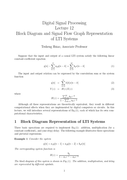
Digital Signal ProcessingLecture12Block Diagram and Signal Flow Graph Representationof LTI SystemsTesheng Hsiao,Associate ProfessorSuppose that the input and output of a causal LTI system satisfy the following linear constant-coefficient equationy[n]−N∑k=1a k y[n−k]=M∑k=0b k x[n−k](1)The input and output relation can be expressed by the convolution sum or the system functiony[n]=∞∑k=0h[k]x[n−k](2)Y(z)=H(z)X(z)(3)whereH(z)=∑Mk=0b k z−k 1−∑Nk=1a k z−kAlthough all these representations are theoretically equivalent,they result in different computational effects when they are implemented by digital computers or circuits.In this lecture,we will introduce several representations of Eq.(1),each of which has its own com-putational characteristics.1Block Diagram Representation of LTI SystemsThree basic operations are required to implement Eq.(1):addition,multiplication(by a constant coefficient),and(one-step)delay.The following example illustrates these operations and pictorial expressions.Example1Consider the systemy[n]=a1y[n−1]+a2y[n−2]+b0x[n]The corresponding system function isH(z)=b01−a1z−a2zThe block diagram of this system is shown in Fig.(1).The addition,multiplication,and delay are represented by different symbols.Figure 1:Block diagram of the system in Example 1Consider the general case,i.e.the system described by Eq.(1).The block diagram is shown in Fig.(2).This realization is called direct form I .In direct form I realization,the output is obtained through two steps:v [n ]=M ∑k =0b k x [n −k ]y [n ]=N ∑k =1a k y [n −k ]+v [n ]or equivalently,V (z )=H ma (z )X (z )={M ∑k =0b k z −k }X (z )Y (z )=H ar (z )V (z )={11−∑N k =1a k z −k }V (z )and H (z )=H ar (z )H ma (z ).Figure 2:Direct Form I representation of an LTI systemSince both H ar(z)and H ma(z)are LIT systems.We can exchange the order and leave the results unaltered.Hence the system can be implemented in a different way:W(z)=H ar(z)X(z)Y(z)=H ma(z)W(z)or equivalently,w[n]=N∑k=1a k w[n−k]+x[n]y[n]=M∑k=0b k w[n−k]This results in the block diagram in Fig.(3).Figure3:Direct Form II representation of an LTI system In Fig.(3),the two columns of delays contains the same values(w[n−k]);hence they can be combined into one column of delays as shown in Fig.(4).The realization in Fig.(4) is called direct form II or canonic direct form.One distinct property of direct form I and II is the number of delays.In other words, the required size of storage space(memory or register)is different.Direct form I contains N+M delays whereas direct form II has max{M,N}delays.Hence direct form II is more efficient in terms of space usage.An implementation with the minimum number of delay elements is commonly referred to as a canonic form implementation.Example2Consider the LTI systemH(z)=1+2z−11−1.5z−1+0.9z−2The direct form I and II implementation are shown in Fig.(5)and Fig.(6)respectively.Figure4:Direct Form II representation of an LTI systemFigure5:Direct form I of Example22Signal Flow Graph Representation of LTI Systems Instead of using block diagrams introduced in the previous section,we usually use signal flow graph to represent a system described by Eq.(1)because signalflow graphs are more compact.A signalflow graph consists of nodes and directed branches.A node denotes a variable or a sequence.A node could have several entering and leaving branches.A branch connects a pair of nodes with an arrow denoting the direction.Each branch represents a linear operation,such as multiplication or delay,on the departure node.The operation carried out by each branch is denoted by that branch.It denotes the unity gain multiplication if there is no notation associated with the branch.The value of a node is the sum of all entering branches.There are two special nodes in the signalflow graph.Source nodes are nodes that have no entering branches.Source nodes are used to represent the injection of external inputs or signal sources into the graph.Sink nodes are nodes that have only entering branches.Sink nodes are used to extract outputs from the graph.Figure6:Direct form II of Example2Fig.(7)illustrates the direct form II and signalflow graph of afirst order IIR system. The equations represented by Fig.(7b)arew1[n]=aw4[n]+x[n]w2[n]=w1[n]w3[n]=b0w2[n]+b1w4[n]w4[n]=w2[n−1]y[n]=w3[n]These equations can be rearranged,eliminating redundant variables,and becomew2[n]=aw2[n−1]+x[n]y[n]=b0w2[n]+b1w2[n−1]which are exactly the equations represented by direct form II.Figure7:(a)Direct form II(b)Signal Flow GraphOn the other hand,given a signalflow graph,we want to derive the system function from it.The z-transform techniques would be useful in this case,as explained by the following example.Example3Given the signalflow graph in Fig.(8).We can write down the equations for each node:w1[n]=w4[n]−x[n]w2[n]=αw1[n]w3[n]=w2[n]+x[n]w4[n]=w3[n−1]y[n]=w2[n]+w4[n]Take z-transform on both sides,we haveW1(z)=W4(z)−X(z)W2(z)=αW1(z)W3(z)=W2(z)+X(z)W4(z)=z−1W3(z)Y(z)=W2(z)+W4(z)Eliminate W1(z)and W3(z),we obtainW2(z)=α(W4(z)−X(z))(4)W4(z)=z−1(W2(z)+X(z))(5)Y(z)=W2(z)+W4(z)Solving Eq.(4)and Eq.(5)simultaneously,we haveW2(z)=α(z−1−1)1−αz−1X(z)W4(z)=z−1(1−α)1−αz−1X(z)Therefore the system function isY(z)=(α(z−1−1)+z−1(1−α)1−αz−1)X(z)=(z−1−α1−αz−1)X(z)Note that the direct form I representation of the system function is shown in Fig.(9).In direct form I representation,2delay elements and two multiplications are required.Direct form II representation needs one delay element but still two multiplications.In the represen-tation of Fig.(8),only one delay element and one multiplication is required.Figure8:Signalflow graph for Example3Figure9:Direct Form I representation of the system function in Example3。
12虚拟仪器 Block Diagram Design

Chap 12Block Diagram DesignVI联合实验室ftp:// labview:labview 个人信箱:hustccms@You Will LearnA. Hierarchical Design B. Dataflow C. Use Good Wiring Techniques D. Error Handling E. Memory and Speed Optimization F. Using Comments in Block Diagram G. Monitoring VI Performance Using the Profile Window H. Block Diagram ChecklistA. Hierarchical DesignOrganize the VIs in the file system to reflect the hierarchical nature of the software. Create a directory for all the VIs for one application and give it ameaningful name, as shown in Figure 3-1.File pathWhen naming VIs, VI libraries, and directories, avoid using characters that are not accepted by all file systems, such as slash (/), backslash (\), colon (:), tilde (~), and so on. Select Tools» Options to make sure the VI Search Path contains <topvi>\* and <foundvi>\*. Avoid creating files with the same name anywhere within the hierarchy.B. DataflowLabVIEW was designed to use a left-to-right and sometimes top-to-bottom layout. Block diagrams should follow this convention. While the positions of program elements do not determine execution order, avoid wiring from right to left. Only wires and structures determine execution orderDataflowBecause the block diagram in the following figure does not follow left-to-right and top-to-bottom layout, it is very difficult to discern how data flows.DataflowUsing left-to-right and top-to-bottom layout, the same block diagram is much clearer, as shown in the following figure.C. Use Good Wiring TechniquesThe Align and Distribute feature in LabVIEW can make it easy to quickly arrange objects on the block diagram to make it easier to see and understand groupings of objects. Placing objects using symmetry and straight lines can make the block diagram easier to read. Some other good wiring tips are.Some other good wiring tips areAvoid placing any wires under any block diagram objects such as subVIs or structures. Add as few bends in the wires as possible while trying to keep the wires short. Avoid creating wires with long complicated paths that can be confusing. Delete any extraneous wires to keep block diagram clean.Some other good wiring tips areAvoid the use of local variables when it is possible to pass the data by wire. Every local variable that reads the data makes a copy of it. Try not to pass wires though structures if the data in the wire itself is not used within the structure. Evenly space parallel wires in straight lines and around corners.D. Error HandlingLabVIEW does not handle errors automatically. VIs and functions return errors in one of two ways—with numeric error codes or with an error cluster. Error handling in LabVIEW follows the dataflow model. As the VI runs, LabVIEW tests for errors at each execution node.Error ClustersThe error clusters located on the Controls» Array&Cluster palette include the following components of information: • status is a Boolean value that reports TRUE if an error occurred. • code is a signed 32-bit integer that identifies the error numerically. • source is a string that identifies where the error occurred.Using While Loops for Error HandlingYou can wire an error cluster to the conditional terminal of a While Loop to stop the iteration of the While Loop. When an error cluster is wired to the conditional terminal, the shortcut menu items Stop if True and Continue if True change to Stop on Error and Continue while Error.Using Case Structures for Error HandlingWhen you wire an error cluster to the selector terminal of a Case structure, the case selector label displays two cases, Error and No Error, and the border of the Case structure changes color—red for Error and green for No Error. If an error occurs, the Case structure executes the Error subdiagram.E. Memory and Speed OptimizationWaits in Loops If speed is not necessary to a While Loop, add a Wait function to avoid the problem of slowing down other tasks. Typically a delay of 50 to 100 MS is sufficient, but other factors in the application might affect the delay.Waits in LoopsThe delay does not have to have any data dependencies, as shown in Figure 3-2.Efficient Use of ArraysIf possible, do not build arrays using the Build Array function within a loop because the function makes repetitive calls to the memory manager. A more efficient method of building an array is to use auto-indexing or pre-size the array and use the Replace Array Element function to place values in it. Similar issues exist when dealing with strings because in memory, LabVIEW handles strings as arrays of characters.Efficient Use of Local and Global VariablesUse global and local variables as sparingly as possible. You can use both global and local variables to write VIs very efficiently. However, if you misuse or abuse global and local variables, the memory usage of the VI increases and the performance is affected.Avoid Unnecessary Data CoercionChoosing the proper data type for the data to be handled can be important in controlling the memory usage of the application.Avoiding coercion dots also can help you reduce unnecessary memory usage and speed.Avoid Unnecessary Front Panel OverheadConsider indicator overhead when designing the VI if performance is a concern for the application. To optimize the performance of the VI, only display the necessary information on the front panel and only send data to indicators if the data is different from what is already displayed.Sizing and PositioningThe size of the block diagram window can affect how readable your LabVIEW code is to others. While it is good to be aware of the size of the block diagram window, it is also very important to ensure that the LabVIEW code that is displayed in it is not too large. Code that requires the user to scroll only horizontally or vertically is acceptable as long as the user does not have to scroll an unreasonable amount to view the entire code.F. Using Comments in Block DiagramUse comments on the block diagrams to explain what the code is doing. Omit labels on function and subVI calls because they tend to be large and unwieldy. Use free labels on wires to identify their use. This is particularly useful for wires coming from shift registers. Use labels on structures to specify the main functionality of that structure. Use labels on constants to specify the nature of the constant.G. Monitoring VI PerformanceYou can use the Profile window to analyze how your application uses execution time and memory. The Profile window displays the performance information for all VIs in memory in an interactive table format. To show the Profile window, select Tools» Advanced» Profile VIs. You must select the Profile Memory Usage option before starting a profiling session. Many of the options in the Profile window are available only after you begin a profiling session.H. Block Diagram ChecklistUse the following checklist to ensure you use proper block diagram design in your VIs. Avoid creating extremely large block diagrams. Limit the scrolling necessary to see in the entire block diagram to one direction. Label controls, important functions, constants, property nodes, local variables, global variables, and structures. Add comments. Use object labels instead of free labels where applicable and scrollable string constants for long comments.Block Diagram ChecklistPlace labels below objects when possible and rightjustify text if label is placed to the left of an object. Use standard, consistent font conventions throughout. Use Size to Text for all text and add carriage returns if necessary. Reduce white space in smaller block diagrams but allow at least 3 or 4 pixels between objects.Block Diagram ChecklistFlow data from left to right. Wires enter from the left and exit to the right, not the top or the bottom. Align and distribute functions, terminals, and constants. Label long wires with small labels with white backgrounds. Do not wire behind objects. Make good use of reusable, testable subVIs.Block Diagram ChecklistMake sure the program can deal with error conditions and invalid values. Save with the most important or the first frame of structures showing. Review for efficiency, especially data copying, and accuracy, especially parts without data dependency.。
SSD590C直流调速器正点转及正反点动详细设置方法
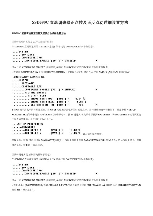
SSD590C直流调速器正点转及正反点动详细设置方法SSD590C直流调速器正点转及正反点动详细设置方法正反转点动的实现方法(开关量端子组态):在SSD590C直流调速器的SYSTEM(系统) 菜单找到 CONFIGURE I/O(参数组态),进入后,将CONFIGURE ENABLE (组态使能)菜单由DISABLE改成ENABLE,再进行如下的操作:1.在菜单CONFIGURE I/O下,找到DIGITAL INPUTS(开关量输入),按M键进入后,找到DIGIN 1 (C6),将C6的目的标记(DESTINATION TAG)改成228。
2.当C4处于高电平的时候是正转,当C4 C6同时处于高电平的时候是反转。
正转反转的速率调整如下:设定参数(SETUP PARAMETERS)菜单中找到JOG/SLACK (点动/放松),按M键进入,在此菜单下找到JOG SPEED 1 和JOG SPEED 2就可以更改正反点动的速率,系统出厂值为正负5%。
最后退出保存参数。
参数保存:按M键直到出现DIAGNOSTS(诊断)后,按向上的键头找到PARAMETER SAVE ,按M进入,然后按向上键头,参数自动保存。
按E键一直退到底。
正反转调速实现方法(开关量端子组态):在SSD590C直流调速器的SYSTEM(系统) 菜单找到 CONFIGURE I/O(参数组态),进入后,将CONFIGURE ENABLE (组态使能)菜单由DISABLE改成ENABLE,再进行如下的操作:1.在此菜单下(CONFIGURE I/O)找到ANALOG INPUTS,在这个菜单下找到ANIN 3(A4),将A4的目的标记(DESTINATION TAG)改成309(原来是5)。
2.在此菜单(CONFIGURE I/O)中找到DIGITAL INPUTS,在这个菜单中找到DIGITL 2(C7),将它的目的标记(DESTINATION TAG)改成292(原来是118)3、在此菜单(CONFIGURE I/O)中找到BLOCK DIAGRAM ,在这个菜单中找到SPT SUM 1 DEST,将它的目的标记改成5(原来是289)。
FPGA轻松学习用QuartusII通过原理图完成与门电路设计

FPGA轻松学习用QuartusII通过原理图完成与门电路设计打开QuartusII软件,程序主界面如下:1,新建一个工程点击File——>New Project Wizard,打开创建新工程向导,这里你将完成工程的基本设定选项。
1,Project name and directory——工程的名称与目录2,Name of the top-level design entity——顶层设计实体的名称3,Project files and libraries——项目文件与库4,Target device family and device——目标设备的族类5,EDA tool settings——EDA工具设定这里一般设定好工程名称和目录,顶层设计实体名称以及目标设备族类就可以了,其他的暂时直接使用默认项就可以了。
2,新建一个设计文件通过点击File——>New打开新建文件选择框,由于我们这里使用原理图描述实现的,则文件类型选择Design Files——>Block Diagram/Schematic File,就新建了一个原理图文件,将其保存起来,注意命名要跟前面设置的顶层设计实体名称相同。
3,编写设计文件接下来开始在文件中绘制原理图,这里首先完成与门的添加,点击左侧工具栏中的Symbol Tool按钮,打开Symbol选择框,选择primitives——>logic——>and2,点击OK后即可在原理图中添加一个2输入的与门了。
在同样通过Symbol Tool中的加入和primitives——>pin——>output加入输入和输出引脚,然后在原理图中把他们用Orthogonal Node Tool即导线连接起来,双击输入输出引脚,为他们设定好名字,pinA,pinB,pinC,就完成了原理图中的设计。
4,编译(分析综合)点击Processing——>Start——>Start Analysis & Synthesis,进行分析综合,就好像是对程序进行编译,等待片刻,如果没有错误,编译报告会输出出来。
飞利浦电视L9H2E维修手册电路图
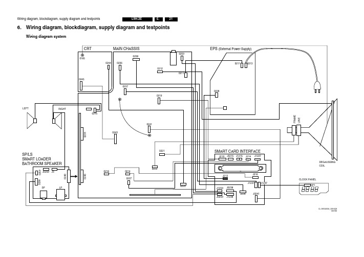
ON A2 to 3400 3431 3433 6431
9
A3 VERTICAL DEFLECTION
VLOT AUX +13V to 2-7460 FOR BASIC SETS LOT 2410 ON A2 to C-6406 -13V
SMPS
I
+5D 2601
SP/LS
6 1 +5V
A8 FRONT CONTROL
SP/LS
+5V
+5VD
+5VD
+5VD
+5Veps
3616-I10 9 CLOCK
3617-D5
3617-C4 4-0238 3-0238 1-0238 ONLY FOR BASIC 4-0238 3-0238 1-0238 Clock Data-in Data-out
SMART PLUG 1 2 5
(PRESENT FOR T1.6A 2W/3W AUDIO)
15
14 7904 PCF8574A
23
24 7951 SAA1064 a
1-0238
0241 1 5
I/O EXPANDER
LED-DRIVER
SYSTEM
+5VD+5VD
FOR SYSTEM SETS ONLY
J SMART CARD INTERFACE
SP/LS
J SMART CARD INTERFACE
32 PIN SMART CARD CONNECTOR VIDEO INTERFACE CIRCUITS AUDIO IIC2
SMART SOUND + MONO AMPLIFIER A10 (ONLY MONO SETS)
Profibus配置提示(第1版)说明书

ObjectiveProvide tips for configuring different Profibus PLC tools used with SSD Drives products EquipmentMaster PLC, Profibus Techbox (6053/6055) or Profibus LinkCard (L5353)ProcedureA LL PLC CONFIGURING TOOLS:Delete all internal software input connections to the drive parameter that the PLC writes to.Otherwise, the internal connection will overwrite the Profibus data to the specified tag number.Any drive parameter with a TAG number can be written to or read from. However, all I/O points that attach to customer connections must be processed properly (triggered). Any function block output under the SYSTEM::CONFIGURE I/O::BLOCK DIAGRAM that is being read by the PLC must be triggered. The examples below show how to trigger correctly.Note: The value for Analog Input 1 is read directly at Setpoint Sum 1::Input 0. The Setpoint Sum 1 block is the trigger for Analog Input 1.Note: The value for Analog Input 2 is read directly at the miniLINK. The miniLINK block is the trigger for Analog Input 2.If you have questions, please call the Product Support Group at (704) 588-3246.The SSD Drives gsd file forces all parameters to be transferred and received as 16-bits.Please visit Resource Center for Profibus manuals and other gsd files.Note: Remember that different configuration tools work differently. Some tools use an import command to install new gsd files. Some copy the gsd to a directory, then either restartthe tool or use a scan gsd command. Other tools just copy the gsd to a directory.Note: The euro3245.gsd requires the first 3 bytes of the User_Param_Data to be set to zeroes.Refer to pages 10 and 11 of HA467329U001 Issue 1.U SING A S IEMENS S7PLC TO CONFIGURE A L5353The following Organization Blocks, OB82, OB85, OB06, and OB122 are “highly” recommended to complete the setup for the PLC. These Organization Blocks keep the PLC from stopping communications and/or simulating a fatal error to the module.Also, uncheck the “Turn on Cyclic Distribution of the Bus Parameters” in the DP monitoring setup. When the PLC has power applied, a Global reset command is initiated and can sometimes simulate a communications error.U SING A GE90_30 PLC WITH V ERSA P RO TO CONFIGURE A 6055/PROF/00The GE Profibus configuration software (Versa Pro) does not support user parameter data larger than 25 bytes in length. The SSD Drives GSD file specifies 63 bytes of user parameter data for the 590+. Users must alter the SSD Drives GSD before importing to the GE hardware configuration software. The end result is that the amount of data that can exchanged between the master and drive is limited to 11 words. GE PLC's do not ground the face of the ProfiBus interface cards or remote I/O, Siemens does.Note: An example connection is on the following pageIf you have questions, please call the Product Support Group at (704) 588-3246.If you have questions, please call the Product Support Group at (704) 588-3246.If you have questions, please call the Product Support Group at (704) 588-3246.ObjectiveTo setup communications between a Siemens PLC S7-315 Master to SSD Drives Profibus communication module L5353.EquipmentS7 PLC, Simatic Manager Step 7 Software, L5300 or L5392, L5311, and L5353. ProcedureNote: The project wizard in Step 7 will guide you to set up the PLC.1. Initialize Simatic Manager2. Select the CPU typeNote: The following blocks are recommended to be added to the PLC configuration OB1,OB82, OB85, OB86, and OB 122.3. Install the Eurotherm Drives GSD file euro5353.gsd.4. Double click on the hardware icon in “Simatic Manager”.5. Select from the pull down menu: Option::Install new GSE.Note: After the “wizard” generates a new project, proceed to step 6 to configure the PLChardware and Profibus Master.If you have questions, please call the Product Support Group at (704) 588-3246.6. Select from the “HW Configure” pull -down menu: Option::Configure Network.7. Next, double click on “DP Master”8. Next, from “Properties – DP Master”, select “Properties”, then assign an address.9. Next, right click on the “X2 DP -Master” of the Hardware Configure, Simatic 300” window, thenselect “Insert DP Master System”.Note: A Profibus(1): DP Master Line appears:10. Select from the pull down menu, “Insert::hardware component”.Note: A hardware window will appear. You can select the Link product as shown.If you have questions, please call the Product Support Group at (704) 588-3246.11. Make sure to install a power supply and any other hardware I/O’s being used.Note: Double click on the “Profibus(1): DP Master” line then select “Properties”, “Networksetting”, “Parameters”, then uncheck the “Turn On Cycle Distribution of Bus Parameters”.12. Install a L5353 in the Profibus listing.13. Add a“L5353 Profibus Link Card” folder from the“Hardware Catalog”.Note: Scroll across and under the “Profibus(1): DP Master” line until the cursor changesinto a “+ sign”.14. Now you can assign a node address to L5353.15. Now add the needed “8 Input word” or “8 Output word” as needed for program.Note: Click on the “(2) L5353 DP -Norm” before you drag and drop.If you have questions, please call the Product Support Group at (704) 588-3246.16. Verify the list of I/O words against the Link Configuration.17. Next, from the pull down menu select “Station::Save and Com pile”18. Close this window and from the “Simatic Manager” highlight the Hardware icon and install.Note: After installing the Link and plc program both LED’s on the L5353 should be green.Note: The following is the data communication monitoring in Link and PLC:ObjectiveProvide tips for different PLC tools to be used with SSD Drives products EquipmentMaster PLC, Communication TechBox (6053/6055) or Communication LinkCard (L53xx) ProcedureF OR A LL DRIVE CONFIGURATIONS REGARDLESS OF PLC TYPE:Delete internal software connections to the drive parameter that will be written to by the PLC.Otherwise, the internal drive connection will overwrite the data to the specific tag number.The SSD Drives datasheet file formats all parameters to be transmitted and received as 16-bit words.Any drive parameter with a tag number can be read or write via the PLC. I/O points that attach to customer connections must be properly triggered in the 590+ drive. Any function block output under the SYSTEM::CONFIGURE I/O::BLOCK DIAGRAM that is being read by the PLC must betriggered. The examples below show how to trigger correctly. The 690+ drive does not require the function block output to be connected to a system block to be triggered.Note: The value for Analog Input 1 is read directly at Setpoint Sum 1::Input 0. The Setpoint Sum 1 block is the trigger for Analog Input 1.Note: The value for Analog Input 2 is read directly at the miniLink. The miniLink block isthe trigger for Analog Input 2.If you have questions, please call the Product Support Group at (704) 588-3246.If you have questions, please call the Product Support Group at (704) 588-3246.Note Product:ApplicationDocument Number: 7707 Keywords: USB to Serial AdapterObjectiveTo facilitate the use of CELite, CELite+, DSD and ConfigEd, on computers not fitted with serial ports. IntroductionThese software packages were originally intended to be used with a serial port but several new computers only have USB ports. This document is a recommendation for using the existing cable with a computer that has only a USB port.Note: This does not apply to operating systems older than Windows XP, due to the lack of drivers supported by these adaptors.EquipmentThe Product Support Group has performed test on several different USB to Serial adaptors. See the picture below. The recommended brands have connected reliably between the PC and unit to be programmed, without errors in the SSD Drives software.Recommended BrandsATEN (model UC232A) /?product&cat=595&Item=UC232AIOGEAR (model GUC232A) /main.php?loc=product&Item=GUC232A SEWELL (model SW-1301) /usbtoserial.aspNote: The Belkin brand of USB to Serial adaptor is not recommended. It performed poorly in ourtests with our equipment.If you have questions, please call the Product Support Group at (704) 588-3246.。
UML的几种图
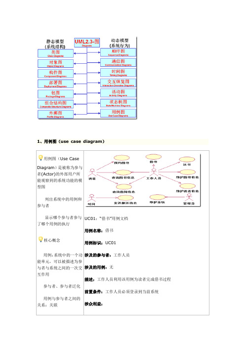
1、用例图(use case diagram)用例图(Use Case Diagram)是被称为参与者(Actor)的外部用户所能观察到的系统功能的模型图列出系统中的用例和参与者显示哪个参与者参与了哪个用例的执行核心概念用例:系统中的一个功能单元,可以被描述为参与者与系统之间的一次交互作用参与者、参与者泛化用例与参与者之间的关系:关联UC01:“借书”用例文档用例名称:借书用例标识:UC01涉及的参与者:工作人员涉及的用例:无描述:工作人员利用该用例为读者完成借书过程前置条件:工作人员必须登录到当前系统涉众利益:用例之间关系:扩展、包括、泛化推荐使用场合 业务建模、需求获取、定义某图书馆管理系统:是一个基于Web 的计算机应用系统; 读者可以查询图书信息以及借阅信息;读者可以通过系统预约所需的图书; 图书馆工作人员利用该系统完成读者的借书、还书业务;图书馆工作人员可以对图书信息、读者信息等进行维护;对于到期的图书,系统会自动向读者发送催还信息;管理员会定期进行系统维护;…… 基本事件流: 后置条件:备选事件流 字段列表: 认为当天日期)、借阅天数以及归还日期。
业务规则 阅规则取决于读者的类型(非功能需求:设计约束:2、活动图(activity diagram)活动图(Activity Diagram)通过动作来组织,主要用于描述某一方法、机制或用例的内部行为核心概念状态、活动、组合活动、对象转移、分支并发、同步泳道推荐使用场合业务建模、需求、类设计3、静态结构图类、、框架、层、描述系统中某一)的内部结构,包括该部分与系统其它部分的交互部件、4、顺序图(Sequence Diagram )顺序图(SequenceDiagram )用于显示对象间的交互活动关注对象之间消息传送的时间顺序核心概念 对象、生命线、激活、交互、消息交互帧(InteractionFrame)推荐使用场合用例分析、用例设计“借书”用例实现的顺序图5、交互纵览图(Interaction Overview Diagram) 交互纵览图(Interaction Overview Diagram) 活动图和顺序图的混合物直观地表达一组相关顺序图之间的流转逻辑 核心概念交互帧分支、转移 推荐使用场合用例分析、用例设计交互纵览图组织多个顺序图6、通信图(Communication Diagram)通信图(Communication Diagram)UML 1.x 中称为协作图(CollaborationDiagram)表示一组对象间关系以及交互活动 核心概念对象、协作角色协作、交互、消息“借书”用例实现的通信图推荐使用场合 用例分析、用例设计7、时间图(Timing Diagram)时间图(TimingDiagram)一种交互图,展现消息跨越不同对象或角色的实际时间信息;具体描述单个或多个对象状态变化的时间点以及维持特定状态的时间段;顺序图是表示交互的主要手段,可以在顺序图中增加时间约束来表明对象状态变化的时间点以及维持特定状态的时间段。
W9412G6JH-5I;中文规格书,Datasheet资料

Read Operation............................................................................................................. 12 Write Operation ............................................................................................................. 13 Precharge ..................................................................................................................... 13 Burst Termination ......................................................................................................... 13 Refresh Operation ........................................................................................................ 13 Power Down Mode ....................................................................................................... 14 Input Clock Frequency Change during Precharge Power Down Mode ........................ 14 Mode Register Operation .............................................................................................. 14 Publication Release Date: Nov. 29, 2011 Revision A03
联想工厂上电时序讲解-新机型PPT课件
LDO LDO
SW 1D1V_S0
1D5V_NEW_S0
LDO
DDR_VREF_S3
1D8V_S0
S3# DCBATOUT_51125
VCC
VIN
PWR_S5_EN
EN
5V_S5
5V_S0
CAMERA SW
S3#
_EN
USB_PWR_EN SW
5V_CAM_S0 5V_USB1_S3
DDR_VREF_S3
3D3V_S0
3D3V_DELAY
U22
S3# VGACORE_PWRGD
LDO 3D3V_BT_S0
LDO LCDVDD_S0
0Ω
3D3V_DVDD33
AD+
5V_S0
1D05V_S0
VCC
G10
Switch
S3# 19V1.05V
EN
1.25V_1.05V_CANTIGA 0Ω
6
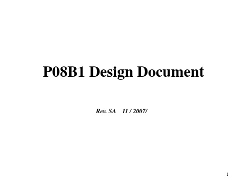
P08B1 Power Budget
H_PWRGD
RESET#
VGATE_PWRGD
3D3V_S0
G792
8
7
CPUCORE_ON
VCC_CORE
240ms after VCC_G792>4.38V
6266A_PWRGOOD
EN
PGOOD
ISL6266A
10
CLK_PWRGD
PWRGOOD
12 RSTIN# Cantiga
PWROK
HCPURST#
ALC269
CLKGEN SRCC6 CLK_PCIE_ICH# (100 MHz)
DMI_CLKN
ICS9LPRS365
PLC基础学习资料(很实用)

在此添加您的文本16字
总结词:应用广泛
在此添加您的文本16字
详细描述:梯形图在工业自动化控制领域应用广泛,几乎 所有的PLC厂商都支持梯形图编程,并且在实际项目中得 到广泛应用。
Function Block Diagram(功能块图)
P按照预期工作,并满足 控制要求。
定期维护
定期对PLC进行维护,包括检查电缆连接、清除 灰尘、更换电池等,以确保其正常运行。
ABCD
故障诊断
通过诊断工具和程序,快速定位和解决PLC故障。
软件更新
及时更新PLC的软件和固件,以获得最新的功能 和修复潜在的漏洞。
详细描述
PLC的硬件主要由电源、中央处理器、输入输出模块、存储器、通信接口等部分组成。电源是整个PLC系统的能 源供给,中央处理器是PLC的控制中心,输入输出模块用于接收和发送信号,存储器用于存储程序和数据,通信 接口用于实现PLC与外部设备的通信。
PLC的软件编程
总结词
学习PLC的软件编程是应用PLC技术的关键, 包括编程语言、编程工具、程序结构等方面 的基础知识和实践操作。
02
PLC编程语言
Ladder Diagram(梯形图)
在此添加您的文本17字
总结词:直观易懂的编程语言
在此添加您的文本16字
详细描述:梯形图是一种类似于电气控制电路的编程语言 ,通过图形化的方式表示输入、输出和中间控制逻辑,易 于理解和实现。
在此添加您的文本16字
总结词:易于学习掌握
在此添加您的文本16字
安全性增强
随着工业安全意识的提高,PLC将加强安 全防护功能,提高设备的安全性和稳定性。
labview学习总结

Block Diagram>Programming>Numeric>conversion>……….1.可以将长整型的十进制数转换为二进制数。
转换格式如下:。
2.正好与“1”相反。
3.将Boolean型(True of False)转换为(1,0)整型量。
4.将字符或字符串转换为相应的无符号ASCII码或ASCII码数组。
如下:5.正好与“4”相反。
6.将0-255之间的r,g,b数值组合转换成颜色。
7.正好与“6”相反。
8.不同类型数据间的转换。
Block Diagram>Programming>Array>……….9.返回矩阵的大小,若是一维矩阵,则返回矩阵的大小;若是二维的,则返回一个数组,分别表示每一维的大小。
如下:10.通过输入索引值在输入数组中返回所选择的元素或一维数组。
如下:输入数组为3X3(0-2,0-2),输入索引值2(第三列),则返回第三列。
11.通过输入索引值,用一维数组来取代原数组中的索引值那一列,返回一个新的数组。
如下:12.通过输入索引值,在原数组中输入一列或一行数组,返回一个新的数组。
若没有索引值,则自动在原数组最后输入一列或一行。
如下:13.通过输入索引值或需删除的数组长度,在原数组中删除一列或一行,返回一个新的数组和被删除的部分。
如下:输入length=2,则在原数组中删除最后2行,返回一个新的数组。
14.通过指定数组元素、行数和列数来初始化数组。
如下:15.将输入的数组或元素按照顺序合成为一个数组并输出。
如下:16.将数组转换为簇。
如下:17.正好与“16”相反。
18.将2维数组转换为实矩阵。
如下:19.正好与“18”相反。
20.将一维数组根据索引值分解为两个子数组。
如下:输入的索引值为n,则取原一维数组的前n个数组成一个子数组,原数组其余的数组成另一个子数组。
21.反转一维数组。
如下:22.通过输入索引值,旋转一维数组,如下:若输入的索引值为n,则输出的一维数组以原数组中的倒数第n个数为开头,顺序排下去。
block_diag函数

block_diag函数block_diag函数是Python中的一个函数,用于构造一个块对角矩阵。
该函数在科学计算、矩阵计算以及信号处理等方面广泛应用。
```numpy.block_diag(*arrs)````*arrs`表示要构造的矩阵块的元组序列,这些矩阵块必须是二维数组。
例如:```pythonimport numpy as npa = np.array([[1, 2], [3, 4]])b = np.array([[5, 6], [7, 8]])c = np.array([[9, 10], [11, 12]])d = np.block([[a, np.zeros((2, 2))], [np.zeros((2, 2)), b], [np.zeros((2,4))]])e = np.block([c, np.identity(2)])print(d)print(e)```输出结果如下:```[[1. 2. 0. 0.][3. 4. 0. 0.][0. 0. 5. 6.][0. 0. 7. 8.][0. 0. 0. 0.][0. 0. 0. 0.]][[ 9. 10. 1. 0.][11. 12. 0. 1.]]```在上述例子中,首先定义了三个矩阵块a、b和c,然后使用`np.block`函数将它们拼接成新的二维数组。
具体来说,`d`是由矩阵块a、b和一个2x4的零矩阵构成,拼接在一起形成的,而`e`则是由矩阵块c和一个2x2的单位矩阵构成。
除了`block_diag`函数外,numpy还提供了一些其他的构造函数,例如`numpy.concatenate`、`numpy.vstack`、`numpy.hstack`等。
这些函数也可以用于构造矩阵块。
不过需要注意的是,这些函数构造的矩阵块必须维度相同,而`block_diag`函数则可以将不同形状的矩阵块拼接在一起,同时在拼接部位填充零矩阵。
第6章 事件管理器(xkj201611)4

QEP1 QEP2 QEPI1
正交编码器脉冲 电路
QEP3 QEP4 QEPI2
定时器的 外部输入
定时器计数方向和 时钟的外部输入
TDIRA TCLKINA
定时器计数方向和时 钟的外部输入
TDIRB TCLKINB
启动外部ADC转换的 输出触发信号
EVASOC
EVBSOC
LOGO
功能概述
EV Device Interfaces
/
2
TCLKINA / TDIRA ADC Start T1PWM_T1CMP
Output Logic
PWM Circuits Output Logic PWM Circuits Output Logic PWM Circuits Output Logic Output Logic
CLK DIR
PWM1 PWM2 PWM3 PWM4 PWM5 PWM6 T2PWM_T2CMP
LOGO
通用定时器计数操作的用途
连续增计数模式特别适用于边沿触发或异步PWM波形 产生,也适用于电机和运动控制系统的采样周期产生
定向增/减计数模式可用于正交编码脉冲电路。正交 编码脉冲电路为通用定时器2或4提供计数时钟和方向。
连续增/减计数模式特别适用于对称PWM波形产生。 该波形广泛应用于电机控制、运动控制和电力电子 设备中。
LOGO
通用定时器的结构
一个可读/写的16位定时器比较寄存器(双缓冲) TxCMPR(x=1、2、3或4)
用于比较操作 设定占空比
一个可读/写的16位定时器周期寄存器(双缓冲) TxPR(x=1、2、3或4)
用于计数操作 设定PWM周期
LOGO
通用定时器的结构
