A Low Dropout, CMOS Regulator with High PSR over Wideband Frequencies
LM1085

−40˚C to 150˚C
Electrical Characteristics
Typicals and limits appearing in normal type apply for TJ = 25˚C. Limits appearing in Boldface type apply over the entire junction temperature range for operation.
60
LM1085-3.3, VIN = 6.3V
60
LM1085-5.0, VIN = 8V
60
LM1085-12 VIN = 15V
54
Adjust Pin Current LM1085
5.5
A
0.5
A
5.5
A
5.5
A
5.5
A
5.0
10.0
mA
5.0
10.0
mA
5.0
10.0
mA
5.0
10.0
mA
150˚C -65˚C to 150˚C 260˚C, to 10 sec
2000V
Operating Ratings (Note 1)
Junction Temperature Range (TJ) (Note 3)
Control Section
−40˚C to 125˚C
Output Section
3-lead TO-220
−40˚C to + 125˚C
Simplified Schematic
Part Number LM1085IS-ADJ LM1085ISX-ADJ LM1085IS-12 LM1085ISX-12 LM1085IS-3.3 LM1085ISX-3.3 LM1085IS-5.0 LM1085ISX-5.0 LM1085IT-ADJ LM1085IT-12 LM1085IT-3.3 LM1085IT-5.0
Richtek RT9049 500mA LDO调压器说明书

1DS9049-01 April 2011Ordering InformationNote :Richtek products are :` RoHS compliant and compatible with the current require-ments of IPC/JEDEC J-STD-020.` Suitable for use in SnPb or Pb-free soldering processes.ApplicationszCDMA/GSM Cellular Handsets z Portable Information Appliancesz Laptop, Palmtops, Notebook Computers z HandHeld Instrumentsz Mini PCI & PCI-Express Cards z PCMCIA & New CardsPin ConfigurationsGeneral DescriptionThe RT9049 is a high-performance, 500mA LDO regulator,offering extremely high PSRR and ultra-low dropout. The RT9049 is designed for portable RF and wireless applications with demanding performance and space requirements. The RT9049 quiescent current is as low as 115μA, further prolonging the battery life. The RT9049 also works with low-ESR ceramic capacitors, reducing the amount of board space necessary which is critical for power applications in hand-held wireless devices. The RT9049 consumes typical 1.35μA in shutdown mode and has fast turn-on time less than 40μs. The other features include ultra-low dropout voltage, high output accuracy,current limiting protection, and high ripple rejection ratio.The RT9049 is available in the SOT-23-5 package.Features500mA, Low Dropout, Low Noise Ultra-Fast Without Bypass Capacitor CMOS LDO RegulatorzWide Operating Voltage Ranges : 2.2V to 5.5V z Low Dropout : 250mV at 500mA z Ultra-Low-Noise for RF Applicationz Ultra-Fast Response in Line/Load Transient z Current Limiting Protection z Thermal Shutdown Protectionz High Power Supply Rejection Ratioz Only 10μF Output Capacitor Required for Stability z 1.35μA Shutdown Currentz TTL-Logic-Controlled Shutdown Input z RoHS Compliant and Halogen FreeSOT-23-5(TOP VIEW)Marking InformationFor marking information, contact our sales representative directly or through a Richtek distributor located in your area.Typical Application CircuitVOUTRT904912 : 1.2V2DS9049-01 April 2011Functional Pin DescriptionFunction Block DiagramENAbsolute Maximum Ratings (Note 1)z Input Voltage, V IN----------------------------------------------------------------------------------------------------------6Vz EN, V EN----------------------------------------------------------------------------------------------------------------------6Vz Power Dissipation, P D @ T A = 25°CSOT-23-5--------------------------------------------------------------------------------------------------------------------0.4Wz Package Thermal Resistance (Note 2)SOT-23-5, θJA---------------------------------------------------------------------------------------------------------------250°C/WSOT-23-5, θJC--------------------------------------------------------------------------------------------------------------25°C/Wz Lead Temperature (Soldering, 10 sec.)-------------------------------------------------------------------------------260°Cz Junction T emperature-----------------------------------------------------------------------------------------------------150°Cz Storage T emperature Range--------------------------------------------------------------------------------------------−65°C to 150°C z ESD Susceptibility (Note 3)HBM (Human Body Mode)----------------------------------------------------------------------------------------------2kVMM (Machine Mode)------------------------------------------------------------------------------------------------------200VRecommended Operating Conditions (Note 4)z Junction T emperature Range--------------------------------------------------------------------------------------------−40°C to 125°C z Ambient T emperature Range--------------------------------------------------------------------------------------------−40°C to 85°C Electrical Characteristics(V IN =2.7V, V EN= V IN, C IN =1μF, C OUT = 10μF(Ceramic, X7R), T A = 25°C, unless otherwise specified)DS9049-01 April 20113Note 1. Stresses listed as the above“Absolute Maximum Ratings”may cause permanent damage to the device. These are for stress ratings. Functional operation of the device at these or any other conditions beyond those indicated in the operational sections of the specifications is not implied. Exposure to absolute maximum rating conditions for extended periods may remain possibility to affect device reliability.Note 2. θJA is measured in the natural convection at T A = 25°C on a low effective thermal conductivity single layer test board of JEDEC 51-3 thermal measurement standard. The case position of θJC is on the package top of the package. Note 3. Devices are ESD sensitive. Handling precaution is recommended.Note 4. The device is not guaranteed to function outside its operating conditions.Note 5. Quiescent, or ground current, is the difference between input and output currents. It is defined by I Q = I IN-I OUT under no load condition (I OUT = 0mA). The total current drawn from the supply is the sum of the load current plus the ground pin current.Note 6. Regulation is measured at constant junction temperature by using a 2ms current pulse. Devices are tested for loadregulation in the load range from 10mA to 500mA.DS9049-01 April 2011 45DS9049-01 April 2011Line Transient Response Time (100μs/Div)3.62.6V IN (1V/Div)20−20V OUT(20mV/Div)V IN = 2.6V to 3.6V, V OUT = 1.2V, I OUT = 100mATypical Operating CharacteristicsOutput Voltage vs. Temperature1.1001.1251.1501.1751.2001.2251.2501.2751.300-50-25255075100125Temperature O u tp u t V o l t a g e (V )(°C)Quiescent Current vs. Temperature8090100110120130140-50-25255075100125Temperature Q ui e s c e n t C u r r e n t (μA )(°C)Load Transient ResponseTime (500μs/Div)V IN = 2.75V, V OUT = 1.2V, I OUT = 10mA to 100mAV OUT (5mV/Div)I OUT(50mA/Div)Power On-Off from EN Time (100μs/Div)V EN (1V/Div)V OUT (0.5V/Div)V IN = 2.75V, V OUT = 1.2V, I OUT = 50mALine Transient ResponseTime (100μs/Div)3.62.6V IN (1V/Div)20−20V OUT(20mV/Div)V IN = 2.6V to 3.6V, V OUT = 1.2V, I OUT = 10mA6DS9049-01 April 2011PSRR-70-60-50-40-30-20-1001020101001000100001000001000000Frequency (Hz)P S R R (d B )Load Transient ResponseTime (500μs/Div)V OUT (5mV/Div)I OUT(100mA/Div)V IN = 2.75V, V OUT = 1.2V, I OUT = 10mA to 300mANoiseTime (10msDiv)V OUT(100μV/Div)V IN = 4.5V (By Battery), V OUT = 1.2V, No LoadNoiseTime (10msDiv)V OUT(100μV/Div)V IN = 4.5V (By Battery), V OUT = 1.2V, I OUT = 10mA7DS9049-01 April 2011Applications InformationLike any low-dropout regulator, the external capacitors used with the RT9049 must be carefully selected for regulator stability and performance. Using a capacitor more than 1μF on the RT9049 is suitable. The input capacitor must be located at a distance of not more than 0.5 inch from the input pin of the IC and returned to a clean analog ground.The capacitor with larger value and lower ESR (equivalent series resistance) provides better PSRR and line-transient response.The output capacitor must meet both requirements for minimum capacitance and ESR in all LDOs application.The RT9049 is designed specifically to work with low ESR ceramic output capacitor in space-saving and performance consideration. Using a ceramic capacitor whose value is at least 10μF with ESR is > 45m Ω on the RT9049 output ensures stability. The RT9049 still works well with output capacitor of other types due to the wide stable ESR range.Figure 1. shows the curves of allowable ESR range as a function of load current for various output capacitor values.Output capacitor of larger capacitance can reduce noise and improve load transient response, stability, and PSRR.The output capacitor should be located at less than 0.5inch from the VOUT pin of the RT9049 and returned to a clean analog ground.Figure 1.Region of Stable C OUT ESR vs. Load CurrentEnableThe RT9049 goes into sleep mode when the Enable pin is in a logic low condition. During this condition, the pass transistor, error amplifier, and bandgap are turned off,reducing the supply current to 1.35μA typical. The Enable pin may be directly tied to V IN to keep the part on. The Enable input is CMOS logic and cannot be left floating.PSRRThe power supply rejection ratio (PSRR) is defined as the gain from the input to output divided by the gain from the supply to the output. The PSRR is found to be ⎟⎟⎠⎞⎜⎜⎝⎛ΔΔ×=Supply Error Gain log 20 PSRR Note that when heavy load measuring, Δsupply will cause Δtemperature. And Δtemperature will cause Δoutputvoltage. So the heavy load PSRR measuring is includes temperature effect.Current LimitThe RT9049 contains an independent current limiter, which monitors and controls the pass transistor's gate voltage,limiting the output current to 0.6A (typ.). The output can be shorted to ground indefinitely without damaging the part.Thermal ConsiderationsFor continuous operation, do not exceed absolute maximum operation junction temperature. The maximum power dissipation depends on the thermal resistance of IC package, PCB layout, the rate of surroundings airflow and temperature difference between junction to ambient.The maximum power dissipation can be calculated by following formula :P D(MAX) = (T J(MAX) − T A ) / θJAWhere T J(MAX) is the maximum operation junction temperature, T A is the ambient temperature and the θJA is the junction to ambient thermal resistance.For recommended operating conditions specification of RT9049, the maximum junction temperature is 125°C. The junction to ambient thermal resistance θJA is layout dependent. For SOT-23-5 package, the thermal resistanceRegion of Stable C OUT ESR vs. Load Current0.010.11101000.10.20.30.40.5Load Current (mA)R e g i o n o f S t a b l e C O U T E S R (Ω)8DS9049-01 April 20119DS9049-01 April 2011Information that is provided by Richtek Technology Corporation is believed to be accurate and reliable. Richtek reserves the right to make any change in circuit design, specification or other related things if necessary without notice at any time. No third party intellectual property infringement of the applications should be guaranteed by users when integrating Richtek products into any application. No legal responsibility for any said applications is assumed by Richtek.Richtek Technology CorporationHeadquarter5F, No. 20, Taiyuen Street, Chupei City Hsinchu, Taiwan, R.O.C.Tel: (8863)5526789 Fax: (8863)5526611Richtek Technology CorporationTaipei Office (Marketing)5F, No. 95, Minchiuan Road, Hsintien City Taipei County, Taiwan, R.O.C.Tel: (8862)86672399 Fax: (8862)86672377Email:*********************Outline DimensionA1HLSOT-23-5 Surface Mount Package。
Step-Down Switching Regulators
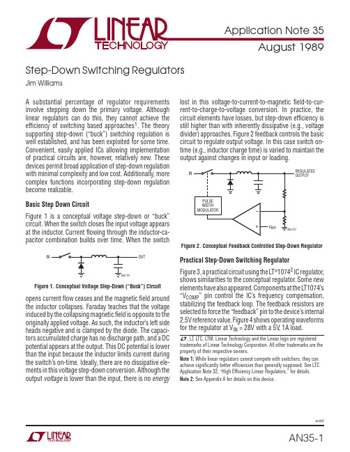
Step-Down Switching RegulatorsJim WilliamsA substantial percentage of regulator requirements involve stepping down the primary voltage. Although linear regulators can do this, they cannot achieve the effi ciency of switching based approaches 1. The theory supporting step-down (“buck”) switching regulation is well established, and has been exploited for some time. Convenient, easily applied ICs allowing implementation of practical circuits are, however , relatively new. These devices permit broad application of step-down regulation with minimal complexity and low cost. Additionally, more complex functions incorporating step-down regulation become realizable.Basic Step Down CircuitF igure 1 is a conceptual voltage step-down or “buck” circuit. When the switch closes the input voltage appears at the inductor . Current fl owing through the inductor-ca-pacitor combination builds over time. When the switchINFigure 1. Conceptual Voltage Step-Down (“Buck”) Circuitopens current fl ow ceases and the magnetic fi eld around the inductor collapses. Faraday teaches that the voltage induced by the collapsing magnetic fi eld is opposite to the originally applied voltage. As such, the inductor’s left side heads negative and is clamped by the diode. The capaci-tors accumulated charge has no discharge path, and a DC potential appears at the output. This DC potential is lower than the input because the inductor limits current during the switch’s on-time. Ideally, there are no dissipative ele-ments in this voltage step-down conversion. Although the output voltage is lower than the input, there is no energylost in this voltage-to-current-to-magnetic fi eld-to-cur-rent-to-charge-to-voltage conversion. In practice, thecircuit elements have losses, but step-down effi ciency is still higher than with inherently dissipative (e.g., voltage divider) approaches. Figure 2 feedback controls the basic circuit to regulate output voltage. In this case switch on-time (e.g., inductor charge time) is varied to maintain the output against changes in input or loading.INFigure 2. Conceptual Feedback Controlled Step-Down RegulatorPractical Step-Down Switching RegulatorFigure 3, a practical circuit using the L T ®10742 IC regulator , shows similarities to the conceptual regulator . Some new elements have also appeared. Components at the L T1074’s “V COMP ” pin control the IC’s frequency compensation, stabilizing the feedback loop. The feedback resistors are selected to force the “feedback” pin to the device’s internal 2.5V reference value. F igure 4 shows operating waveforms for the regulator at V IN = 28V with a 5V , 1A load.L , L T , L TC, L TM, Linear Technology and the Linear logo are registered trademarks of Linear Technology Corporation. All other trademarks are the property of their respective owners.Note 1: While linear regulators cannot compete with switchers, they can achieve signifi cantly better effi ciencies than generally supposed. See L TC Application Note 32, “High Effi ciency Linear Regulators,” for details.Note 2: See Appendix A for details on this device.T race A is the V SW pin voltage and T race B is its current. Inductor current 3 appears in T race C and diode current is T race D. Examination of the current waveforms allows determination of the V SW and diode path contributions to inductor current. Note that the inductor current’s waveform occurs on top of a 1A DC level. Figure 5 shows signifi cant duty cycle changes when V IN is reduced to 12V . The lower input voltage requires longer inductor charge times to maintain the output. The L T1074 controls inductor charge characteristics (see Appendix A for operating details), with resulting waveform shape and time proportioning changes.F igure 6 compares this circuit’s effi ciency with linear regulators in a common and important situation. Effi cient regulation under varying AC line conditions is a frequent requirement. The fi gure assumes the AC line has been transformed down to acceptable input voltages. The input voltages shown correspond to the AC line voltages given on the horizontal axis. Effi ciency for the LM317 and L T1086 linear regulators suffers over the wide input range.Note 3: Methods for selecting appropriate inductors are discussed in Appendix B.L1V INFigure 3. A Practical Step-Down Regulator Using the L T1074Figure 4. Waveforms for the Step-Down Regulator at V IN = 28V and V OUT = 5V at 1AAC LINE VOLTAGE800E F F I C I E N C Y (%)20406090100110120AN35 F06130801001030507090140Figure 6. Efficiency vs AC Line Voltage for the LT1074. LT1086 and LM317 Linear Regulators are Shown for ComparisonFigure 5. Waveforms for the Step-Down Regulator at V IN = 12V and V OUT = 5V at 1AA = 20V/DIVB = 1A/DIV D = 1A/DIVHORIZ = 5μs/DIVAN35 F04C = 0.2A/DIV ON 1A DC LEVELA = 20V/DIVB = 1A/DIV D = 1A/DIVHORIZ = 5μs/DIVAN35 F05C = 0.2A/DIV ON 1A DC LEVELThe L T1086 is notably better because its lower dropout voltage cuts dissipation over the range. Switching pre-regulation 4 can reduce these losses, but cannot equal the L T1074’s performance. The plot shows minimum effi ciency of 83%, with some improvement over the full AC line excursion. Figure 7 details performance. Effi ciency approaches 90% as input voltage rises. This is due to minimization of the effects of fi xed diode and L T1074 junc-tion losses as input increases. At low inputs these losses are a higher percentage of available supply, degrading effi ciency. Higher inputs make the fi xed losses a smaller percentage, improving effi ciency. Appendix D presents detail on optimizing circuitry for effi ciency.Note 4: See Reference 1.Dual Output Step-Down RegulatorFigure 8, a logical extension of the basic step-down con-verter , provides positive and negative outputs. The circuit is essentially identical to Figure 3’s basic converter with the addition of a coupled winding to L1. This fl oating winding’s output is rectifi ed, fi ltered and regulated to a –5V output. The fl oating bias to the L T1086 positive voltage regulator permits negative outputs by assigning the regulator’s output terminal to ground. Negative output power is set by fl ux pick-up from L1’s driven winding. With a 2A load at the +15 output the –5V output can supply over 500mA. Because L1’s secondary winding is fl oating its output may be referred to any point within the breakdown capability of the device. Hence, the secondary output could be 5V or , if stacked on the +15 output, 20V .Negative Output RegulatorsNegative outputs can also be obtained with a simple 2-ter-minal inductor . Figure 9 demonstrates this by essentially grounding the inductor and steering the catch diodes negative current to the output. A1 facilitates loop closure by providing a scaled inversion of the negative output to the L T1074’s feedback pin. The 1% resistors set the scale factor (e.g., output voltage) and the RC network around A1 gives frequency compensation. Waveforms for this circuit are reminiscent of Figure 5, with the exception that diodeINPUT VOL TAGEE F F I C I E N C Y (%)608010024AN35 F0740205070903010012101614202226183028Figure 7. Efficiency Plot for Figure 3. Higher Input Voltages Minimize Effects of Saturation Losses, Resulting in Increased EfficiencyL1: PULSE ENGINEERING, INC. #PE-6505028VINPUTAN35 F08Figure 8. Coupled Inductor Provides Positive and Negative Outputscurrent (T race D) is negative. T races A, B and C are V SW voltage, inductor current and V SW current respectively.Figure 11, commonly referred to as “Nelson’s Circuit,” provides the same function as the previous circuit, but eliminates the level-shifting op amp. This design accom-plishes the level shift by connecting the L T1074’s “ground” pin to the negative output. Feedback is sensed from circuit ground, and the regulator forces its feedback pin 2.5V above its “ground” pin. Circuit ground is common to input and output, making system use easy. Operating waveforms are essentially identical to Figure 10. Advantages of the previous circuit compared to this one are that the L T1074 package can directly contact a grounded heat sink and that control signals may be directly interfaced to the ground referred pins.The inductor values in both negative output designs are notably lower than in the positive case. This is necessitatedby the reduced loop phase margin of these circuits. Higher inductance values, while preferable for limiting peak cur-rent, will cause loop instability or outright oscillation.Current-Boosted Step-Down RegulatorF igure 12 shows a way to obtain signifi cantly higher output currents by utilizing effi cient energy storage in the L T1074 output inductor . This technique increases the duty cycle over the standard step-down regulator allowing more energy to be stored in the inductor . The increased output current is achieved at the expense of higher output voltage ripple.The operating waveforms for this circuit are shown in Figure 13. The circuit operating characteristics are similar to that of the step-down regulator (Figure 3). During the V SW (T race A) “on” time the input voltage is applied to one end of the coupled inductor . Current through the V SW pin (T race B) ramps up almost instantaneously (since inductor current (T race F) is present) and then slows as energy is stored in the core. The current proceeds into the inductor (T race D) and fi nally is delivered to the load. When the V SW pin goes off, current is no longer available to charge the inductor . The magnetic fi eld collapses, causing the V SW pin voltage to go negative. At this point similarity with the basic regulator vanishes. In this modifi ed version the output current (T race F) receives a boost as the magnetic fi eld collapses. This results when the energy stored in12V INPUT–5V OUTPUTFigure 9. A Negative Output Step-Down RegulatorFigure 10. Figure 9’s WaveformsA = 20V/DIVB = 1A/DIV D = 4A/DIVHORIZ = 5μs/DIVAN35 F10C = 4A/DIVthe core is transferred to the output. This current step circulates through C1 and D2 (T race E), somewhat increas-ing output voltage ripple. Not all the energy is transferred to the “1” winding. Current (T race C) will continue to fl ow in the “N” winding due to leakage inductance. A snubber network suppresses the effects of this leakage inductance. For lowest snubber losses the specifi ed tapped inductor is bifi lar wound for maximum coupling.Post Regulation-Fixed CaseIn most instances the L T1074 output will be applied directly to the load. Those cases requiring faster transient responseor reduced noise will benefi t from linear post regulation. In F igure 14 a 3-terminal regulator follows the L T1074 output. The L T1074 output is set to provide just enough voltage to the L T1084 to maintain regulation. The L T1084’s low dropout characteristics combined with a high circuit input voltage minimizes the overall effi ciency penalty.OUT VFigure 11. Nelson’s Circuit...A (Better) Negative Output Step-Down Regulator5V OUT10AVFigure 12. “Current Boosted” Step-Down Regulator. Boost Current is Supplied By Energy Stored in the Tapped InductorFigure 13. AC Current Flow for the Boosted RegulatorA = 50V/DIVB = 5A/DIVD = 10A/DIVE = 10A/DIVF = 10A/DIVHORIZ = 2μs/DIV AN35 F10C = 10A/DIVPost Regulation-Variable CaseSome situations require variable linear post regulation. F igure 15 does this with little effi ciency sacrifi ce. The L T1085 operates in normal fashion, supplying a variable 1.2V to 28V output. The remainder of the circuit forms a switched mode pre-regulator which maintains a small, fi xed voltage across the L T1085 regardless of its output voltage. A1 biases the L T1074 to produce whatever voltage is necessary to maintain the “E diodes” potential across the L T1085. A1’s inputs are balanced when the L T1085 output is “E diodes” above its input. A1 maintains this condition regardless of line, load or output voltage conditions. Thus, good effi ciency is maintained over the full range of output voltages. The RC network at A1 compensates the loop. Loop start-up is assured by deliberately introduc-ing a positive offset to A1. This is done by grounding A1’s appropriate balance pin (5), resulting in a positive 6mV offset. This increases amplifi er drift, and is normally considered poor practice, but causes no measurable error in this application.As shown, the circuit cannot produce outputs below the L T1085’s 1.2V reference. Applications requiring output adjustability down to 0V will benefi t from option “A” shown on the schematic. This arrangement replaces L1 with L2. L2’s primary performs the same function as L1 and its coupled secondary winding produces a negative bias output (–V). The full-wave bridge rectifi cation is necessitated by widely varying duty cycles. A2 and its at-tendant circuitry replace all components associated withthe L T1085 V ADJ pin. The L T1004 reference terminates the 10k to 250k feedback string at –1.2V with A2 provid-ing buffered drive to the L T1085 V ADJ pin. The negative bias allows regulated L T1085 outputs down to 0V . The –V potential derived from L2’s secondary varies consider-ably with operating conditions. The high feedback string values and A2’s buffering ensure stable circuit operation for “starved” values of –V .Low Quiescent Current RegulatorsMany applications require very wide ranges of power sup-ply output current. Normal conditions require currents in the ampere range, while standby or “sleep” modes draw only microamperes. A typical laptop computer may draw 1 to 2 amperes running while needing only a few hundred microamps for memory when turned off. In theory, any regulator designed for loop stability under no-load condi-tions will work. In practice, a converter’s relatively large quiescent current may cause unacceptable battery drain during low output current intervals. Figure 16’s simple loop effectively reduces circuit quiescent current from 6mA to only 150μA. It does this by utilizing the L T1074’s shutdown pin. When this pin is pulled within 350mV of ground the IC shuts down, pulling only 100μA. Comparator C1 combines with the L T1004 reference and Q1 to form a “bang-bang” control loop around the L T1074. The L T1074’s internal feedback amplifi er and voltage reference are by-passed by this loop’s operation. When the circuit output (T race C, Figure 17) falls slightly below 5V C1’s output (T race A) switches low, turning off Q1 and enabling theL1V IN5V OUTFigure 14. Linear Post-Reglator Improves Noise and T ransient ResponseL1: PULSE ENGINEERING, INC. #PE-51516L2: PULSE ENGINEERING, INC. #PE-6505035V INPUTOUTAN35 F15OPTION “A”(FOR OUTPUT DOWN TO 0V)SEE TEXT FOR DISCUSSIONL112V INPUT5V OUTFigure 15. Adjustable Linear Post-Regulator Maintains Efficiency Over Widely Varying Operating ConditionsFigure 16. A Simple Loop Reduces Quiescent Current to 150μAL T1074. The V SW pin (T race B) pulses at full duty cycle, forcing the output back above 5V . C1 then biases Q1 again, the L T1074 goes into shutdown, and loop action repeats.The frequency of this on-off control action is directly load dependent, with typical repetition rates of 0.2Hz at no load. Short on-times keep duty cycle low, resulting in the small effective quiescent current noted. The on-off operation combines with the LC fi ltering action in the regulator’s V SW line to generate an output hysteresis of about 50mV (again, see Figure 17, T race C).The loop performs well, but has two potential drawbacks. At higher output currents the loop oscillates in the 1kHz to 10kHz range, causing audible noise which may be objec-tionable. This is characteristic of this type of loop, and is the reason that ICs employing gated oscillators invariably produce such noise. Additionally, the control loops opera-tion causes about 50mV of ripple on the output. Ripple frequency ranges from 0.2Hz to 10kHz depending upon input voltage and output current.Figure 18’s more sophisticated circuit eliminates these problems with some increase in complexity. Quiescent current is maintained at 150μA. The technique shown is particularly signifi cant, with broad implication in battery powered systems. It is easily applied to a wide variety of regulator requirements, meeting an acknowledged need across a wide spectrum of applications.Figure 18’s signal fl ow is similar to Figure 16, but ad-ditional circuitry appears between the feedback divider and the L T1074. The L T1074’s internal feedback amplifi er and reference are not used. Figure 19 shows operatingFigure 17. The Low Quiescent Current Loop’s WaveformsV IN–+12VFigure 18. A More Sophisticated Loop Gives Better Regulation While Maintaining 150μA Quiescent CurrentA = 10V/DIVB = 10V/DIV HORIZ = 100μs/DIVAN35 F17C = 0.1V/DIV AC-COUPLED ON 5V DC LEVELwaveforms under no-load conditions. The output (T race A) ramps down over a period of seconds. During this time comparator A1’s output (T race B) is low, as are the 74C04 paralleled inverters. This pulls the V C pin (T race D) low, forcing the regulator to zero duty cycle. Simultaneously, A2 (T race C) is low, putting the L T1074 in its 100μA shutdown mode. The V SW pin (T race E) is off, and no inductor current fl ows. When the output drops about 60mV , A1 triggers and the inverters go high, pulling the V C pin up and biasing the regulator . The Zener diode prevents V C pin overdrive. A2 also rises, taking the IC out of shutdown mode. The V SW pin pulses the inductor at the 100kHz clock rate, causing the output to abruptly rise. This action trips A1 low, forcing the V C pin back low and shutting off V SW pulsing. A2 also goes low, putting the L T1074 into shutdown.This “bang-bang” control loop keeps the 5V output within the 60mV ramp hysteresis window set by the loop. Note that the loop oscillation period of seconds means the R1-C1time constant at V C is not a significant term. Because the L T1074 spends almost all of the time in shutdown, very little quiescent current (150μA) is drawn.Figure 20 shows the same waveforms with the load in-creased to 2mA. Loop oscillation frequency increases to keep up with the load’s sink current demand. Now, the V C pin waveform (T race D) begins to take on a fi ltered ap-pearance. This is due to R1-C1’s 10ms time constant. If the load continues to increase, loop oscillation frequency will also increase. The R1-C1 time constant, however , is fi xed. Beyond some frequency, R1-C1 must average loop oscillations to DC. At 7mA loading (Figure 21) loop fre-quency further increases, and the V C waveform (T race D) appears heavily fi ltered.Figure 22 shows the same circuit points at 2A loading. Note that the V C pin is at DC, as is the shutdown pin. Repetition rate has increased to the L T1074’s 100kHzFigure 19. Low Quiescent Current Regulator’s Waveforms with No Load (T races B, C and E Retouched for Clarity)Figure 20. Low Quiescent Current Regulator’s Waveforms at 2mA LoadingFigure 21. Low Quiescent Current Regulator’s Waveforms at 7mA Loading Figure 22. Low Quiescent Current Regulator’s Waveforms at 2A LoadingA = 0.1V/DIV AC-COUPLEDB = 20V/DIV HORIZ = 0.5 SECOND/DIVAN35 F19C = 20V/DIVD = 2V/DIVE = 10V/DIVA = 0.1V/DIV AC-COUPLEDB = 20V/DIV HORIZ = 20ms/DIVAN35 F20C = 20V/DIVD = 2V/DIVE = 10V/DIVA = 0.1V/DIV AC-COUPLEDB = 20V/DIV HORIZ = 10ms/DIVAN35 F21C = 20V/DIVD = 2V/DIVE = 10V/DIVA = 0.2V/DIV AC-COUPLEDB = 20V/DIV HORIZ—TRACES A AND E = 10μs/DIV TRACES B, C, D = 5ms/DIVAN35 F22C = 20V/DIVD = 2V/DIVE = 20V/DIVclock frequency. Figure 23 plots what is occurring, with a pleasant surprise. As output current rises, loop oscilla-tion frequency also rises until about 23Hz. At this point the R1-C1 time constant fi lters the V C pin to DC and the L T1074 transitions into “normal” PWM operation. With the V C pin at DC it is convenient to think of A1 and the inverters as a linear error amplifi er with a closed-loop gain set by the R2-R3 feedback divider . In fact, A1 is still duty cycle modulating, but at a rate far above R1-C1’s break frequency. The phase error contributed by C2 (which was selected for low loop frequency at low output currents) is dominated by the R1-C1 roll off and the C3 lead into A1. The loop is stable and responds linearly for all loads beyond 10mA. In this high current region the L T1074 is desirably “fooled” into behaving like a conventional step-down regulator .A formal stability analysis for this circuit is quite complex, but some simplifi cations lend insight into loop operation. At 250μA loading (20kΩ) C2 and the load form a decay time constant exceeding 30 seconds. This is orders of magnitude larger than R2-C3, R1-C1, or the L T1074’s 100kHz commutation rate. As a result, C2 dominates the loop. Wideband A1 sees phase shifted feedback, and very low frequency oscillations similar to Figure 19’s occur 5. Although C2’s decay time constant is long, its charge time constant is short because the circuit has low sourc-ing impedance. This accounts for the ramp nature of the oscillations.Increased loading reduces the C2-load decay time con-stant. Figure 23’s plot refl ects this. As loading increases,the loop oscillates at a higher frequency due to C2’s de-creased decay time. When the load impedance becomes low enough C2’s decay time constant ceases to dominate the loop. This point is almost entirely determined by R1 and C1. Once R1 and C1 “take over” as the dominant time constant the loop begins to behave like a linear system. In this region (e.g., above about 10mA, per Figure 23) the L T1074 runs continuously at its 100kHz rate. Now, C3 becomes signifi cant, performing as a simple feedback lead 6 to smooth output response. There is a fundamental trade-off in the selection of the C3 lead value. When the converter is running in its linear region it must dominate the loops time lag generated hysteretic characteristic. As such, it has been chosen for the best compromise between output ripple at high load and loop transient response.Despite the complex dynamics transient response is quite good. Figure 24 shows performance for a step from no load to 1A. When T race A goes high a 1A load appears across the output (T race C). Initially, the output sags al-most 200mV due to slow loop response time (the R1-C1 pair delay V C pin (T race B) response). When the L T1074 comes on response is reasonably quick and surprisingly well behaved considering circuit dynamics. The multi-time constant recovery 7 (“rattling” is perhaps more appropriate) is visible in T race C’s response.Note 5: Some layouts may require substantial trace area to A1’s inputs. In such cases the optional RC network around A1 ensures clean transitions at A1’s output.Note 6: “Zero Compensation” for all you technosnobs out there.Note 7: Once again, “multi-pole settling” for those who adore jargon.OUTPUT (mA)L O O P F R E Q U E N C Y (H z )4812162468AN35 F23101220Figure 23. Figure 18’s Loop Frequency vs Output Current. Note Linear Loop Operation Above 10mAFigure 24. Load T ransient Response for Figure 18A = 10V/DIVB = 2V/DIVHORIZ = 5ms/DIVAN35 F24C = 0.2V/DIV ON 5V DC LEVELF igure 25 plots effi ciency versus output current. High power effi ciency is similar to standard converters. Low power effi ciency is somewhat better , although poor in the lowest ranges. This is not particularly bothersome, as power loss is very small.The loop provides a controlled, conditional instability instead of the usually more desirable (and often elusive) unconditional stability. This deliberately introduced char-acteristic dramatically lowers converter quiescent current without sacrifi cing high power performance.a toroidal DC/DC converter comprised of L1, Q1 and Q2. Q1 and Q2 receive out of phase square wave drive from the 74C74 ÷ 4 fl ip-fl op stage and the L T1010 buffers. The fl ip-fl op is clocked from the L T1074 V SW output via the Q3 level shifter . The L T1086 provides 12V power for A1 and the 74C74. A1 biases the L T1074 regulator to produce the DC input at the DC/DC converter required to balance to loop. The converter has a voltage gain of about 20, resulting in high voltage output. This output is resistively divided down, closing the loop at A1’s negative input. Frequency compensation for this loop must accommodate the signifi -cant phase errors generated by the L T1074 confi guration, the DC/DC converter and the output LC fi lter . The 0.47μF roll-off term at A1 and the 100Ω-0.15μF RC lead network provide the compensation, which is stable for all loads.Figure 27 gives circuit waveforms at 500V output into a 100W load. T race A is the L T1074 V SW pin while T race B is its current. T races C and D are Q1 and Q2’s drain waveforms. The disturbance at the leading edges is due to cross-current conduction, which lasts about 300ns—a small percent-age of the cycle. T ransistor currents during this interval remain within reasonable values, and no overstress or dissipation problems occur . This effect could be eliminated with non-overlapping drive to Q1 and Q28, although there would be no reliability or signifi cant effi ciency gain. The 500kHz ringing on the same waveforms is due to excita-tion of transformer resonances. These phenomena are not deleterious, although L1’s primary RC damper is included to minimize them.All waveforms are synchronous because the fl ip-fl op drive stage is clocked from the L T1074 V SW output. The L T1074’s maximum 95% duty cycle means that the Q1-Q2 switches can never see destructive DC drive. The only condition allowing DC drive occurs when the L T1074 is at zero duty cycle. This case is clearly non-destructive, because L1 receives no power .Figure 28 shows the same circuit points as Figure 27, but at only 5mV output. Here, the loop restricts drive to the DC/DC converter to small levels. Q1 and Q2 chop just 70mV into L1. At this level L1’s output diode drops look large, but loop action forces the desired 0.005V output.OUTPUT CURRENTE F F I C I E N C Y (%)6080100 2.0AN35 F254020507090301000.51.01.52.5Figure 25. Efficiency vs Output Current for Figure 18. Standby Efficiency is Poor , But Power Loss Approaches Battery Self-DischargeWide Range, High Power , High Voltage Regulator BEFORE PROCEEDING ANY FURTHER, THE READER IS WARNED THAT CAUTION MUST BE USED IN THE CONSTRUCTION, TESTING AND USE OF THIS CIRCUIT . HIGH VOL TAGE, LETHAL POTENTIALS ARE PRESENT IN THIS CIRCUIT . EXTREME CAUTION MUST BE USED IN WORKING WITH AND MAKING CONNECTIONS TO THIS CIRCUIT . REPEAT : THIS CIRCUIT CONTAINS DANGER-OUS, HIGH VOL TAGE POTENTIALS. USE CAUTION.Figure 26 is an example of the L T1074 making a complex function practical. This regulator provides outputs from mil-livolts to 500V at 100W with 80% effi ciency. A1 compares a variable reference voltage with a resistively scaled version of the circuit’s output and biases the L T1074 switching regulator confi guration. The switcher’s DC output drivesNote 8: For an example of this technique see L TC Application Note 29, Figure 1.T 28V I N100μS O L I T A N T A L U F i g u r e 26. L T 1074 P e r m i t s H i g h V o l t a g e O u t p u t O v e r 100d B R a n g e w i t h P o w e r a n d E f f i c i e n c y .D A N G E R ! L e t h a l P o t e n t i a l s P r e s e n t —S e e T e x tThe L T1074’s switched mode drive to L1 maintains high effi ciency at high power , despite the circuits wide output range 9.Figure 29 shows output noise at 500V into a 100W load. Q1-Q2 chopping artifacts and transformer related ringing are clearly visible, although limited to about 80mV . The coherent noise characteristic is traceable to the synchro-nous clocking of Q1 and Q2 by the L T1074.A 50V to 500V step command into a 100W load produces the response of Figure 30. Loop response on both edgesis clean, with the falling edge slightly underdamped. This slew asymmetry is typical of switching confi gurations, because the load and output capacitor determine negative slew rate. The wide range of possible loads mandates a compromise when setting frequency compensation. The falling edge could be made critically or even over damped, but response time for other conditions would suffer . The compensation used seems a reasonable compromise.Note 9: A circuit related to the one presented here appears in the L TC Application Note 18 (Figure 13). Its linear drive to the step-up DC/DC converter forces dissipation, limiting output power to about 15W . Similar restrictions apply to Figure 7 in Application Note 6.Figure 27. Figure 26’s Operating Waveforms at 500V Output into a 100W LoadFigure 28. Figure 26’s Operating Waveforms at 0.005V OutputFigure 29. Figure 26’s Output Noise at 500V into a 100W Load. Residue is Composed of Q1-Q2 Chopping Artifacts and T ransformer Related Ringing. DANGER! Lethal Potentials Present—See TextFigure 30. 500V Step Response with 100W Load (Photo Retouched for Clarity). DANGER! Lethal Potentials Present—See TextA = 50V/DIVB = 5A/DIVHORIZ = 10μs/DIVAN35 F27C = 50V/DIVD = 50V/DIVA = 5V/DIVB = 50mA/DIVHORIZ = 10μs/DIVAN35 F28C = 0.1V/DIVD = 0.1V/DIVA = 0.05V/DIV AC-COUPLED ON 500V LEVELHORIZ = 20μs/DIVAN35 F29A = 100V/DIVHORIZ = 50ms/DIVAN35 F30。
DS_BL9110--1A Low Dropout Low Iq High PSRR CMOS LDO(EN,V1.1)

PCMCIA Cards and Wireless LAN Electrical appliances such as cameras, VCRS
DESCRIPTION
The BL9110 is a low-dropout regulator that operates the input voltage from 2.5V to 6V and delivers 1A load current. The BL9110 is available in two types, either fixed or adjustable output voltage. The output voltage of the fixed types is preset at an internally trimmed voltage 1V, 1.2V, 1.3V, 1.5V, 1.8V, 2.5V, 2.7V, 2.8V, 2.85V, 3.0V, 3.2V, 3.3V, 5V or can be made with options of the output range from 1V to 5V in 50mV increments. The output range of adjustable types is from 1V to 5V. The BL9110 consists of a voltage reference, an error amplifier, resistor net for setting output voltage, a current limit circuit for over-current and a thermal-shutdown circuit. A standby mode with ultra low supply current can be realized with the chip enable function. Since the packages for BL9110 are DFN-6, SOT-89-5, SOT-223-5, SOT-223-3, TO-263-3, TO-220-3, SOT-89-3, TO-252-3, TO92-3 and TO-252-5 with high power dissipation, high density mounting of the IC on board is possible.
高压降稳压管7133
The 71XX-1 series is a family of Low Dropout Positive regulators developed using CMOS technology. These ICS perform with high output voltage accuracy, low quiescent current ,The allow operation voltage as high as 24V.
典型值 XX
50 50 100 400 2.0
0.2
最大值
XX *102%
24 100 85
4.0
单位 V
mA mV mV Ta μA
%/V
温度调整率
∆VOUT ∆Ta
IOUT =30mA -45℃ ≤Ta≤85℃
+/-0.3
mV/℃
注:
1. VOUT (T)& “XX” :规定的输出电压; XX:X.XV 例如:71(XX)A-1#;XX 为 30 时 :输出:3.0V。 2. VOUT (E) :有效输出电压( 即当 IOUT 保持一定数值,VIN = (VOUT (T)+0.8V)时的输出电压。) 3. Vdif :VIN1 –VOUT (E)’
71XX-1
50mA,高输入电压 LDO 线性稳压器
1
低压差 CMOS 电压稳压器 71XX-1 系列
Low Dropout CMOS Voltage Regulator 71XX-1 Series
71XX-1 系列是使用 CMOS 技术开发 的低压差型正电压稳压电路。具有高 输出电压精度,低静态功耗电流,且 最高工作电压可达 24V 的特点。
VIN1 :逐渐减小输入电压,当输出电压降为 VOUT (E) 的 98%时的输入电压。 VOUT (E)’= VOUT (E)X98%
S-818_1资料

Table 2 Pin No. Symbol Pin description 1 VIN Input voltage pin 2 VSS GND pin 3 ON/OFF Shutdown pin NC*1 No connection 4 5 VOUT Output voltage pin *1. The NC pin is electrically open. The NC pin can be connected to VIN or VSS.
1
2
3
Figure 2
元器件交易网
Rev.2.1_00
LOW DROPOUT CMOS VOLTAGE REGULATOR
S-818 Series
The S-818 Series is a positive voltage regulator developed by CMOS technology and featured by low dropout voltage, high output voltage accuracy and low current consumption. Built-in low on-resistance transistor provides low dropout voltage and large output current. A ceramic capacitor of 2 µF or more can be used as an output capacitor. A shutdown circuit ensures long battery life. The SOT-23-5 miniaturized package and the SOT-89-5 package are recommended for configuring portable devices and large output current applications, respectively.
LP3876-ADJ中文资料

LP3876-ADJ3A Fast Ultra Low Dropout Linear RegulatorGeneral DescriptionThe LP3876-ADJ fast ultra low-dropout linear regulators op-erate from a +2.5V to +7.0V input supply.These ultra low dropout linear regulators respond very quickly to step changes in load,which makes them suitable for low voltage microprocessor applications.The LP3876-ADJ is developed on a CMOS process which allows low quiescent current operation independent of output load current.This CMOS process also allows the LP3876-ADJ to operate under ex-tremely low dropout conditions.Dropout Voltage:Ultra low dropout voltage;typically 80mV at 300mA load current and 800mV at 3A load current.Ground Pin Current:Typically 6mA at 3A load current.Shutdown Mode:Typically 1µA quiescent current when the shutdown pin is pulled low.Adjustable Output Voltage:The output voltage may be programmed via two external resistors.Featuresn Ultra low dropout voltage n Low ground pin current n Load regulation of 0.08%n 1µA quiescent current in shutdown mode n Guaranteed output current of 3A DCn Available in TO-263and TO-220packages n Minimum output capacitor requirements n Overtemperature/overcurrent protectionn−40˚C to +125˚C junction temperature rangeApplicationsn Microprocessor power suppliesn GTL,GTL+,BTL,and SSTL bus terminators n Power supplies for DSPs n SCSI terminator n Post regulatorsn High efficiency linear regulators n Battery chargersnOther battery powered applicationsTypical Application Circuit20074445*See Application HintsSeptember 2003LP3876-ADJ 3A Fast Ultra Low Dropout Linear Regulator©2003National Semiconductor Corporation Connection Diagrams20074405Top View TO220-5Package Bent,Staggered Leads20074406Top View TO263-5PackagePin Description for TO220-5and TO263-5PackagesPin #LP3876-ADJName Function1SD Shutdown 2V IN Input Supply 3GND Ground 4V OUT Output Voltage 5ADJSet Output VoltageOrdering Information20074431Package Type Designator is "T"for TO220package,and "S"for TO263package.TABLE 1.Package Marking and Ordering InformationOutput Voltage Order Number Current DescriptionPackage Type Package Marking Supplied As:ADJ LP3876ES-ADJ 3A TO263-5LP3876ES-ADJ RailADJ LP3876ESX-ADJ 3A TO263-5LP3876ES-ADJ Tape and Reel ADJLP3876ET-ADJ3ATO220-5LP3876ET-ADJRailL P 3876-A D J 2LP3876-ADJ Block Diagram LP3876-ADJ3Absolute Maximum Ratings(Note 1)If Military/Aerospace specified devices are required,please contact the National Semiconductor Sales Office/Distributors for availability and specifications.Storage Temperature Range −65˚C to +150˚CLead Temperature (Soldering,5sec.)260˚C ESD Rating (Note 3)2kVPower Dissipation (Note 2)Internally Limited Input Supply Voltage (Survival)−0.3V to +7.5V Shutdown Input Voltage (Survival)−0.3V to 7.5V Output Voltage (Survival),(Note 6),(Note 7)−0.3V to +6.0V I OUT (Survival)Short Circuit ProtectedOperating RatingsInput Supply Voltage (Operating),(Note 10)2.5V to 7.0V Shutdown Input Voltage (Operating)−0.3V to 7.0VMaximum Operating Current (DC)3AOperating Junction Temp.Range−40˚C to +125˚CElectrical Characteristics LP3876-ADJLimits in standard typeface are for T J =25˚C,and limits in boldface type apply over the full operating temperature range .Unless otherwise specified:V IN =V O(NOM)+1.5V,I L =10mA,C OUT =10µF,V SD =2V.SymbolParameterConditionsTyp (Note 4)LP3876-ADJ (Note 5)UnitsMin Max V ADJ Adjust Pin Voltage V OUT +1.5V ≤V IN ≤7V 10mA ≤I L ≤3A 1.216 1.1981.1801.2341.253V I ADJ Adjust Pin Input Current V OUT +1.5V ≤V IN ≤7V 10mA ≤I L ≤3A 10100nA ∆V OL Output Voltage Line Regulation (Note 8)V OUT +1.5V ≤V IN ≤7.0V 0.020.06%∆V O /∆I OUTOutput Voltage Load Regulation (Note 8)10mA ≤I L ≤3A0.080.14%V IN -V OUT Dropout Voltage (Note 9)I L =300mA 80105125mVI L =3A 80010001200I GNDGround Pin Current In Normal Operation Mode I L =300mA5910mAI L =3A 61415I GND Ground Pin Current In Shutdown Mode V SD ≤0.3V 110µA-40˚C ≤T J ≤85˚C 50I O(PK)Peak Output Current V O ≥V O(NOM)-4%4.5A SHORT CIRCUIT PROTECTIONI SCShort Circuit Current6AL P 3876-A D J 4Electrical CharacteristicsLP3876-ADJ(Continued)Limits in standard typeface are for T J=25˚C,and limits in boldface type apply over the full operating temperature range. Unless otherwise specified:V IN=V O(NOM)+1.5V,I L=10mA,C OUT=10µF,V SD=2V.Symbol Parameter Conditions Typ(Note4)LP3876-ADJ(Note5)Units Min MaxSHUTDOWN INPUTV SDT Shutdown Threshold Output=High V IN2V Output=Low00.3T dOFF Turn-off delay I L=3A20µs T dON Turn-on delay I L=3A25µsI SD SD Input Current V SD=V IN1nA AC PARAMETERSPSRR Ripple Rejection V IN=V OUT+1VC OUT=10uFV OUT=3.3V,f=120Hz73dB V IN=V OUT+0.5VC OUT=10uFV OUT=3.3V,f=120Hz57ρn(l/f Output Noise Density f=120Hz0.8µVe n Output Noise Voltage BW=10Hz–100kHzV OUT=2.5V150µV(rms) BW=300Hz–300kHzV OUT=2.5V100Note1:Absolute maximum ratings indicate limits beyond which damage to the device may occur.Operating ratings indicate conditions for which the device isintended to be functional,but does not guarantee specific performance limits.For guaranteed specifications and test conditions,see Electrical Characteristics.The guaranteed specifications apply only for the test conditions listed.Some performance characteristics may degrade when the device is not operated under the listedtest conditions.Note2:At elevated temperatures,devices must be derated based on package thermal resistance.The devices in TO220package must be derated atθjA=50˚C/W(with0.5in2,1oz.copper area),junction-to-ambient(with no heat sink).The devices in the TO263surface-mount package must be derated atθjA=60˚C/W(with0.5in2,1oz.copper area),junction-to-ambient.See Application Hints.Note3:The human body model is a100pF capacitor discharged through a1.5kΩresistor into each pin.Note4:Typical numbers are at25˚C and represent the most likely parametric norm.Note5:Limits are guaranteed by testing,design,or statistical correlation.Note6:If used in a dual-supply system where the regulator load is returned to a negative supply,the output must be diode-clamped to ground.Note7:The output PMOS structure contains a diode between the V IN and V OUT terminals.This diode is normally reverse biased.This diode will get forward biasedif the voltage at the output terminal is forced to be higher than the voltage at the input terminal.This diode can typically withstand200mA of DC current and1Ampof peak current.Note8:Output voltage line regulation is defined as the change in output voltage from the nominal value due to change in the input line voltage.Output voltage load regulation is defined as the change in output voltage from the nominal value due to change in load current.Note9:Dropout voltage is defined as the minimum input to output differential voltage at which the output drops2%below the nominal value.Dropout voltage specification applies only to output voltages of2.5V and above.For output voltages below2.5V,the drop-out voltage is nothing but the input to output differential,since the minimum input voltage is2.5V.Note10:The minimum operating value for V IN is equal to either[V OUT(NOM)+V DROPOUT]or2.5V,whichever is greater.LP3876-ADJ5Typical Performance CharacteristicsUnless otherwise specified:T J =25˚C,C OUT =10µF,C IN =10µF,S/D pin is tied to V IN ,V OUT =2.5V,V IN=V O(NOM)+1.5V,I L =10mADropout Voltage Vs Output Load CurrentGround Current vs Output Load CurrentV OUT =5V2007446220074453Ground Current vs Output VoltageIL=3AShutdown I Q vs Junction Temperature2007445420074455DC Load Reg.vs Junction Temperature DC Line Regulation vs Temperature2007445820074459L P 3876-A D J 6Typical Performance Characteristics Unless otherwise specified:TJ=25˚C,C OUT=10µF,C IN=10µF,S/D pin is tied to V IN,V OUT=2.5V,V IN=V O(NOM)+1.5V,I L=10mA(Continued)V IN vs V OUT Over Temperature Noise vs Frequency2007446020074461Load Transient Response C IN=C OUT=10µF,OSCONLoad Transient ResponseC IN=C OUT=100µF,OSCON 2007448620074487Load Transient Response C IN=C OUT=100µF,POSCAPLoad Transient ResponseC IN=C OUT=10µF,TANTALUM2007448820074489LP3876-ADJ 7Typical Performance Characteristics Unless otherwise specified:T J =25˚C,C OUT =10µF,C IN =10µF,S/D pin is tied to V IN ,V OUT =2.5V,V IN =V O(NOM)+1.5V,I L =10mA (Continued)Load Transient Response C IN =C OUT =100µF,TANTALUMLoad Transient Response C IN =C OUT =10µF,OSCON2007449020074491Load Transient Response C IN =C OUT =100µF,OSCON Load Transient Response C IN =C OUT =100µF,POSCAP2007449220074493Load Transient Response C IN =C OUT =10µF,TANTALUM Load Transient Response C IN =C OUT =100µF,TANTALUM2007449420074495L P 3876-A D J 8Application HintsV IN RESTRICTIONS FOR PROPER START-UPTo prevent misoperation,ensure that V IN is below50mVbefore start-up is initiated.This scenario can occur in sys-tems with a backup battery using reverse-biased"blocking"diodes which may allow enough leakage current to flow intothe V IN node to raise it’s voltage slightly above ground whenthe main power is ing low leakage diodes or aresistive pull down can prevent the voltage at V IN from risingrge bulk capacitors connected to V IN mayalso cause a start-up problem if they do not discharge fullybefore re-start is initiated(but only if V IN is allowed to fallbelow1V).A resistor connected across the capacitor willallow it to discharge more quickly.It should be noted that theprobability of a"false start"caused by incorrect logic statesis extremely low.SETTING THE OUTPUT VOLTAGEThe output voltage is set using the resistors R1and R2(seeTypical Application Circuit).The output is also dependent onthe reference voltage(typically1.216V)which is measuredat the ADJ pin.The output voltage is given by the equation:V OUT=V ADJ x(1+R1/R2)This equation does not include errors due to the bias currentflowing in the ADJ pin which is typically about10nA.Thiserror term is negligible for most applications.If R1is> 100kΩ,a small error may be introduced by the ADJ biascurrent.The tolerance of the external resistors used contributes asignificant error to the output voltage accuracy,with1%resistors typically adding a total error of approximately1.4%to the output voltage(this error is in addition to the toleranceof the reference voltage at V ADJ).EXTERNAL CAPACITORSLike any low-dropout regulator,external capacitors are re-quired to assure stability.these capacitors must be correctlyselected for proper performance.INPUT CAPACITOR:An input capacitor of at least1µF isrequired.Ceramic or Tantalum may be used,and capaci-tance may be increased without limitOUTPUT CAPACITOR:An output capacitor is required forloop stability.It must be located less than1cm from thedevice and connected directly to the output and ground pinsusing traces which have no other currents flowing throughthem(see PCB Layout section).The minimum value of the output capacitance that can beused for stable full-load operation is10µF,but it may beincreased without limit.The output capacitor must have anESR value as shown in the stable region of the curve(be-low).ESR Curve20074470C FF(Feed Forward Capacitor)The capacitor C FF is required to add phase lead and helpimprove loop compensation.The correct amount of capaci-tance depends on the value selected for R1(see TypicalApplication Circuit).The capacitor should be selected suchthat the zero frequency as given by the equation shownbelow is approximately45kHz:Fz=45,000=1/(2xπx R1x C FF)A good quality ceramic with X5R or X7R dielectric should beused for this capacitor.SELECTING A CAPACITORIt is important to note that capacitance tolerance and varia-tion with temperature must be taken into consideration whenselecting a capacitor so that the minimum required amountof capacitance is provided over the full operating tempera-ture range.In general,a good Tantalum capacitor will showvery little capacitance variation with temperature,but a ce-ramic may not be as good(depending on dielectric type).Aluminum electrolytics also typically have large temperaturevariation of capacitance value.Equally important to consider is a capacitor’s ESR changewith temperature:this is not an issue with ceramics,as theirESR is extremely low.However,it is very important in Tan-talum and aluminum electrolytic capacitors.Both show in-creasing ESR at colder temperatures,but the increase inaluminum electrolytic capacitors is so severe they may notbe feasible for some applications(see Capacitor Character-istics Section).CAPACITOR CHARACTERISTICSCERAMIC:For values of capacitance in the10to100µFrange,ceramics are usually larger and more costly thantantalums but give superior AC performance for bypassinghigh frequency noise because of very low ESR(typically lessthan10mΩ).However,some dielectric types do not havegood capacitance characteristics as a function of voltageand temperature.Z5U and Y5V dielectric ceramics have capacitance thatdrops severely with applied voltage.A typical Z5U or Y5Vcapacitor can lose60%of its rated capacitance with half ofthe rated voltage applied to it.The Z5U and Y5V also exhibitLP3876-ADJ9Application Hints(Continued)a severe temperature effect,losing more than 50%of nomi-nal capacitance at high and low limits of the temperature range.X7R and X5R dielectric ceramic capacitors are strongly rec-ommended if ceramics are used,as they typically maintain a capacitance range within ±20%of nominal over full operat-ing ratings of temperature and voltage.Of course,they are typically larger and more costly than Z5U/Y5U types for a given voltage and capacitance.TANTALUM:Solid Tantalum capacitors are recommended for use on the output because their typical ESR is very close to the ideal value required for loop compensation.They also work well as input capacitors if selected to meet the ESR requirements previously listed.Tantalums also have good temperature stability:a good quality Tantalum will typically show a capacitance value that varies less than 10-15%across the full temperature range of 125˚C to −40˚C.ESR will vary only about 2X going from the high to low temperature limits.The increasing ESR at lower temperatures can cause oscil-lations when marginal quality capacitors are used (if the ESR of the capacitor is near the upper limit of the stability range at room temperature).ALUMINUM:This capacitor type offers the most capaci-tance for the money.The disadvantages are that they are larger in physical size,not widely available in surface mount,and have poor AC performance (especially at higher fre-quencies)due to higher ESR and ESL.Compared by size,the ESR of an aluminum electrolytic is higher than either Tantalum or ceramic,and it also varies greatly with temperature.A typical aluminum electrolytic can exhibit an ESR increase of as much as 50X when going from 25˚C down to −40˚C.It should also be noted that many aluminum electrolytics only specify impedance at a frequency of 120Hz,which indicates they have poor high frequency performance.Only aluminum electrolytics that have an impedance specified at a higher frequency (between 20kHz and 100kHz)should be used for the LP387X.Derating must be applied to the manufacturer’s ESR specification,since it is typically only valid at room temperature.Any applications using aluminum electrolytics should be thoroughly tested at the lowest ambient operating tempera-ture where ESR is maximum.PCB LAYOUTGood PC layout practices must be used or instability can be induced because of ground loops and voltage drops.The input and output capacitors must be directly connected to the input,output,and ground pins of the LP387X using traces which do not have other currents flowing in them (Kelvin connect).The best way to do this is to lay out C IN and C OUT near the device with short traces to the V IN ,V OUT ,and ground pins.The regulator ground pin should be connected to the exter-nal circuit ground so that the regulator and its capacitors have a "single point ground".It should be noted that stability problems have been seen in applications where "vias"to an internal ground plane were used at the ground points of the IC and the input and output capacitors.This was caused by varying ground potentials atthese nodes resulting from current flowing through the ground ing a single point ground technique for the regulator and it’s capacitors fixed the problem.Since high current flows through the traces going into V IN and coming from V OUT ,Kelvin connect the capacitor leads to these pins so there is no voltage drop in series with the input and output capacitors.RFI/EMI SUSCEPTIBILITYRFI (radio frequency interference)and EMI (electromagnetic interference)can degrade any integrated circuit’s perfor-mance because of the small dimensions of the geometries inside the device.In applications where circuit sources are present which generate signals with significant high fre-quency energy content (>1MHz),care must be taken to ensure that this does not affect the IC regulator.If RFI/EMI noise is present on the input side of the regulator (such as applications where the input source comes from the output of a switching regulator),good ceramic bypass ca-pacitors must be used at the input pin of the IC.If a load is connected to the IC output which switches at high speed (such as a clock),the high-frequency current pulses required by the load must be supplied by the capacitors on the IC output.Since the bandwidth of the regulator loop is less than 100kHz,the control circuitry cannot respond to load changes above that frequency.The means the effective output impedance of the IC at frequencies above 100kHz is determined only by the output capacitor(s).In applications where the load is switching at high speed,the output of the IC may need RF isolation from the load.It is recommended that some inductance be placed between the output capacitor and the load,and good RF bypass capaci-tors be placed directly across the load.PCB layout is also critical in high noise environments,since RFI/EMI is easily radiated directly into PC traces.Noisy circuitry should be isolated from "clean"circuits where pos-sible,and grounded through a separate path.At MHz fre-quencies,ground planes begin to look inductive and RFI/EMI can cause ground bounce across the ground plane.In multi-layer PCB applications,care should be taken in layout so that noisy power and ground planes do not radiate directly into adjacent layers which carry analog power and ground.OUTPUT NOISENoise is specified in two ways-Spot Noise or Output noise density is the RMS sum of all noise sources,measured at the regulator output,at a spe-cific frequency (measured with a 1Hz bandwidth).This type of noise is usually plotted on a curve as a function of fre-quency.Total output Noise or Broad-band noise is the RMS sum of spot noise over a specified bandwidth,usually several decades of frequencies.Attention should be paid to the units of measurement.Spot noise is measured in units µV/√Hz or nV/√Hz and total output noise is measured in µV(rms).The primary source of noise in low-dropout regulators is the internal reference.In CMOS regulators,noise has a low frequency component and a high frequency component,which depend strongly on the silicon area and quiescent current.Noise can be reduced in two ways:by increasing the transistor area or by increasing the current drawn by the internal reference.Increasing the area will decrease the chance of fitting the die into a smaller package.IncreasingL P 3876-A D J10Application Hints(Continued)the current drawn by the internal reference increases the total supply current(ground pin current).Using an optimized trade-off of ground pin current and die size,LP387X achieves low noise performance and low quiescent current operation.The total output noise specification for LP387X is presented in the Electrical Characteristics table.The Output noise den-sity at different frequencies is represented by a curve under typical performance characteristics.SHORT-CIRCUIT PROTECTIONThe LP3876-ADJ is short circuit protected and in the event of a peak over-current condition,the short-circuit control loop will rapidly drive the output PMOS pass element off.Once the power pass element shuts down,the control loop will rapidly cycle the output on and off until the average power dissipation causes the thermal shutdown circuit to respond to servo the on/off cycling to a lower frequency.Please refer to the section on thermal information for power dissipation calculations.SHUTDOWN OPERATIONA CMOS Logic level signal at the shutdown(SD)pin will turn-off the regulator.Pin SD must be actively terminated through a10kΩpull-up resistor for a proper operation.If this pin is driven from a source that actively pulls high and low (such as a CMOS rail to rail comparator),the pull-up resistor is not required.This pin must be tied to Vin if not used. DROPOUT VOLTAGEThe dropout voltage of a regulator is defined as the minimum input-to-output differential required to stay within2%of the nominal output voltage.For CMOS LDOs,the dropout volt-age is the product of the load current and the Rds(on)of the internal MOSFET.REVERSE CURRENT PATHThe internal MOSFET in LP3876-ADJ has an inherent para-sitic diode.During normal operation,the input voltage is higher than the output voltage and the parasitic diode is reverse biased.However,if the output is pulled above the input in an application,then current flows from the output to the input as the parasitic diode gets forward biased.The output can be pulled above the input as long as the current in the parasitic diode is limited to200mA continuous and1A peak.POWER DISSIPATION/HEATSINKINGThe LP3876-ADJ can deliver a continuous current of3A over the full operating temperature range.A heatsink may be required depending on the maximum power dissipation and maximum ambient temperature of the application.Under all possible conditions,the junction temperature must be within the range specified under operating conditions.The total power dissipation of the device is given by:P D=(V IN−V OUT)I OUT+(V IN)I GNDwhere I GND is the operating ground current of the device (specified under Electrical Characteristics).The maximum allowable temperature rise(T Rmax)depends on the maximum ambient temperature(T Amax)of the appli-cation,and the maximum allowable junction temperature (T Jmax):T Rmax=T Jmax−T AmaxThe maximum allowable value for junction to ambient Ther-mal Resistance,θJA,can be calculated using the formula:θJA=T Rmax/P DThe LP3876-ADJ is available in TO-220and TO-263pack-ages.The thermal resistance depends on amount of copperarea or heat sink,and on air flow.If the maximum allowablevalue ofθJA calculated above is≥60˚C/W for TO-220package and≥60˚C/W for TO-263package no heatsink isneeded since the package can dissipate enough heat tosatisfy these requirements.If the value for allowableθJA fallsbelow these limits,a heat sink is required.HEATSINKING TO-220PACKAGEThe thermal resistance of a TO220package can be reducedby attaching it to a heat sink or a copper plane on a PCboard.If a copper plane is to be used,the values ofθJA willbe same as shown in next section for TO263package.The heatsink to be used in the application should have aheatsink to ambient thermal resistance,θHA≤θJA−θCH−θJC.In this equation,θCH is the thermal resistance from the caseto the surface of the heat sink andθJC is the thermal resis-tance from the junction to the surface of the case.θJC isabout3˚C/W for a TO220package.The value forθCH de-pends on method of attachment,insulator,etc.θCH variesbetween1.5˚C/W to2.5˚C/W.If the exact value is unknown,2˚C/W can be assumed.HEATSINKING TO-263PACKAGEThe TO-263package uses the copper plane on the PCB asa heatsink.The tab of these packages are soldered to thecopper plane for heat sinking.Figure1shows a curve for theθJA of TO-263package for different copper area sizes,usinga typical PCB with1ounce copper and no solder mask overthe copper area for heat sinking.As shown in the figure,increasing the copper area beyond1square inch produces very little improvement.The minimumvalue forθJA for the TO-263package mounted to a PCB is32˚C/W.Figure2shows the maximum allowable power dissipationfor TO-263packages for different ambient temperatures,assumingθJA is35˚C/W and the maximum junction tempera-ture is125˚C.20074432FIGURE1.θJA vs Copper(1Ounce)Area for TO-263packageLP3876-ADJ11Application Hints(Continued)20074433FIGURE 2.Maximum power dissipation vs ambienttemperature for TO-263packageL P 3876-A D J 12LP3876-ADJ Physical Dimensions inches(millimeters)unless otherwise noted ArrayTO2205-lead,Molded,Stagger Bend Package(TO220-5)NS Package Number T05DFor Order Numbers,refer to the“Ordering Information”section of this document.13Physical Dimensionsinches (millimeters)unless otherwise noted (Continued)TO2635-Lead,Molded,Surface Mount Package (TO263-5)NS Package Number TS5BFor Order Numbers,refer to the “Ordering Information”section of this document.LIFE SUPPORT POLICYNATIONAL’S PRODUCTS ARE NOT AUTHORIZED FOR USE AS CRITICAL COMPONENTS IN LIFE SUPPORT DEVICES OR SYSTEMS WITHOUT THE EXPRESS WRITTEN APPROVAL OF THE PRESIDENT AND GENERAL COUNSEL OF NATIONAL SEMICONDUCTOR CORPORATION.As used herein:1.Life support devices or systems are devices or systems which,(a)are intended for surgical implant into the body,or (b)support or sustain life,and whose failure to perform when properly used in accordance with instructions for use provided in the labeling,can be reasonably expected to result in a significant injury to the user.2.A critical component is any component of a life support device or system whose failure to perform can be reasonably expected to cause the failure of the life support device or system,or to affect its safety or effectiveness.National Semiconductor Americas Customer Support CenterEmail:new.feedback@ Tel:1-800-272-9959National SemiconductorEurope Customer Support CenterFax:+49(0)180-5308586Email:europe.support@Deutsch Tel:+49(0)6995086208English Tel:+44(0)8702402171Français Tel:+33(0)141918790National Semiconductor Asia Pacific Customer Support CenterEmail:ap.support@National SemiconductorJapan Customer Support Center Fax:81-3-5639-7507Email:jpn.feedback@ Tel:81-3-5639-7560L P 3876-A D J 3A F a s t U l t r a L o w D r o p o u t L i n e a r R e g u l a t o rNational does not assume any responsibility for use of any circuitry described,no circuit patent licenses are implied and National reserves the right at any time without notice to change said circuitry and specifications.。
SIIS1142 电压稳压器

Features
• Output voltage :
2.0 V to 12.0 V, selectable in 0.1 V step
• Low equivalent series resistance capacitor : Ceramic capacitor of 0.1 μF or more can be used as the I/O capacitor.
S-1142 Series
© Seiko Instruments Inc., 2009-2010
HIGH-WITHSTAND VOLTAGE LOW CURRENT CONSUMPTION LOW DROPOUT CMOS VOLTAGE REGULATOR
Rev.2.0_00
Remark 1. Please contact our sales office for products with an output voltage other than those listed above or type A products.
2. Please select products of environmental code = U for Sn 100%, halogen-free products.
• Output current :
During shutdown: 0.1 μA typ., 1.0 μA max. (Tj = −40°C to +105°C) 200 mA (at VIN ≥ VOUT(S) + 2.0 V)*1
• Built-in overcurrent protector :
HSOP-6 (+85°C supported) S-1142B20I-E6T1U S-1142B25I-E6T1U S-1142B27I-E6T1U S-1142B28I-E6T1U S-1142B2JI-E6T1U S-1142B30I-E6T1U S-1142B32I-E6T1U S-1142B33I-E6T1U S-1142B35I-E6T1U S-1142B37I-E6T1U S-1142B40I-E6T1U S-1142B50I-E6T1U S-1142B80I-E6T1U
美国半导体CM3202-02 DDR VDDQ和VTT终端电压调节器数据手册说明书
CM3202-02DDR VDDQ and VTT Termination Voltage RegulatorProduct DescriptionThe CM3202−02 is a dual−output low noise linear regulator designed to meet SSTL−2 and SSTL−3 specifications for DDR−SDRAM V DDQ supply and termination voltage V TT supply. With integrated power MOSFETs the CM3202−02 can source up to 2A of VDDQ continuous current, and source or sink up to 2 A VTT continuous current. The typical dropout voltage for VDDQ is 500 mV at 2 A load current.The CM3202−02 provides excellent full load regulation and fast response to transient load changes. It also has built−in over−current limits and thermal shutdown at 170°C.The CM3202−02 supports Suspend−To−RAM (STR) and ACPI compliance with Shutdown Mode which tri−states VTT to minimize quiescent system current.The CM3202−02 is available in a space saving WDFN8 surface mount packages. Low thermal resistance allows them to withstand high power dissipation at 85°C ambient. The CM3202−02 can operate over the industrial ambient temperature range of –40°C to 85°C. Features•Two Linear Regulators•Maximum 2 A Current from VDDQ•Source and Sink Up to 2 A VTT Current•1.7 V to 2.8 V Adjustable VDDQ Output V oltage•0.85 V to 1.4 V VTT Output V oltage (Tracking at 50% of VDDQ)•500 mV Typical VDDQ Dropout V oltage at 2 A •Excellent Load and Line Regulation, Low Noise•Meets JEDEC DDR−I and DDR−II Memory Power Spec •Linear Regulator Design Requires no Inductors and Has Low External Component Count•Integrated Power MOSFETs•Dual Purpose ADJ/Shutdown Pin•Built−In Over−Current Limit and Thermal Shutdown for V DDQ and V TT•Fast Transient Response•Low Quiescent Current•These Devices are Pb−Free and are RoHS CompliantApplications•DDR Memory and Active Termination Buses •Desktop Computers, Servers •Residential and Enterprise Gateways •DSL Modems •Routers and Switches•DVD Recorders•3D AGP Cards•LCD TV and STBMARKING DIAGRAMDevice Package Shipping†ORDERING INFORMATIONCM3202−02DE WDFN8(Pb−Free)3000/T ape & Reel†For information on tape and reel specifications,including part orientation and tape sizes, pleaserefer to our Tape and Reel Packaging SpecificationBrochure, BRD8011/D.CM320 202DE= CM3202−02DECM320202DEWDFN8DE SUFFIXCASE 511BHTYPICAL APPLICATIONV IN = 3.3 V to 3.6 VFUNCTIONAL BLOCK DIAGRAMVTTGNDPACKAGE / PINOUT DIAGRAMSTop View(Pins Down View)Thermal PadCM3202−02DETable 1. PIN DESCRIPTIONSPin(s)Name Description1VIN Input supply voltage pin. Bypass with a 220 m F capacitor to GND.2NC Not internally connected. For better heat flow, connect to GND (exposed pad).3VTT V TT regulator output pin, which is preset to 50% of V DDQ.4NC Not internally connected. For better heat flow, connect to GND (exposed pad).5GND Ground pin (analog).6GND Ground pin (power).7ADJSD This pin is for V DDQ output voltage adjustment. It is available as long as V DDQ is enabled.During Manual/Thermal shutdown, it is tightened to GND. The V DDQ output voltage is setusing an external resistor divider connected to ADJSD:V DDQ = 1.25 V ×((R1 + R2) / R2)Where R1 is the upper resistor and R2 is the ground−side resistor. In addition, the ADJSD pin functions as aShutdown pin. When ADJSD voltage is higher than 2.7 V (SHDN_H), the circuit is in Shutdown mode. WhenADJSD voltage is below 1.5 V (SHDN_L), both VDDQ and VTT are enabled. A low−leakage Schottky diode inseries with ADJSD pin is recommended to avoidinterference with the voltage adjustment setting.8VDDQ VDDQ regulator output voltage pin.EPad GND The backside exposed pad which serves as the package heatsink. Must be connected to GND.SPECIFICATIONSTable 2. ABSOLUTE MAXIMUM RATINGSParameter Rating Units VIN to GND[GND − 0.3] to +6.0VPin VoltagesV DDQ, V TT to GND ADJSD to GND [GND − 0.3] to +6.0[GND − 0.3] to +6.0VOutput CurrentVDDQ / VTT, continuous (Note 1) VDDQ / VTT, peakVDDQ Source + VTT Source 2.0 / ±2.02.8 / ±2.83ATemperature Operating Ambient Operating Junction Storage –40 to +85–40 to +170–40 to +150°CThermal Resistance, R JA (Note 2)55°C / W Continuous Power Dissipation (Note 2)WDFN8, T A = 25°C / 85°C 2.6 / 1.5WESD Protection (HBM)2000VLead Temperature (soldering, 10 sec)300°C Stresses exceeding Maximum Ratings may damage the device. Maximum Ratings are stress ratings only. Functional operation above the Recommended Operating Conditions is not implied. Extended exposure to stresses above the Recommended Operating Conditions may affect device reliability.1.Despite the fact that the device is designed to handle large continuous/peak output currents, it is not capable of handling these under allconditions. Limited by the package thermal resistance, the maximum output current of the device cannot exceed the limit imposed by the maximum power dissipation value.2.Measured with the package using a 4 in2 / 2 layers PCB with thermal vias.Table 3. STANDARD OPERATING CONDITIONSParameter Rating Units Ambient Operating Temperature Range–40 to +85°CVDDQ RegulatorSupply Voltage, VINLoad Current, Continuous Load Current, Peak (1 sec) C DDQ 3.0 to 3.60 to 22.5220VAAm FVTT RegulatorSupply Voltage, VINLoad Current, Continuous Load Current, Peak (1 sec) C TT 3.0 to 3.60 to ±2.0±2.50220VAAm FVIN Supply Voltage Range 3.0 to 3.6VVDDQ Source + VTT Source Load Current, Continuous Load Current, Peak (1 sec)2.53.5AJunction Operating Temperature Range–40 to +150°CSPECIFICATIONS (Cont’d)Table 4. ELECTRICAL OPERATING CHARACTERISTICS (Note 1)Symbol Parameter Conditions Min Typ Max Units GeneralVIN Supply Voltage Range 3.0 3.6VI Q Quiescent Current I DDQ = 0, I TT = 0715mA V ADJSD ADJSD Voltage 1.225 1.250 1.275VI SHDN Shutdown Current V ADJSD = 3.3 V (Shutdown) (Note 3)0.20.5mA SHDN_H ADJSD Logic High(Note 2) 2.7V SHDN_L ADJSD Logic Low 1.5V UVLO Under−Voltage Lockout Hysteresis = 100 mV 2.40 2.70 2.90VT OVER Thermal SHDN Threshold150170°C T HYS Thermal SHDN Hysteresis50°C TEMPCO V DDQ, V TT TEMPCO I OUT = 1 A80ppm/°C VDDQ RegulatorV DDQ DEF VDDQ Output Voltage I DDQ = 100 mA 2.450 2.500 2.550VV DDQ LOAD VDDQ Load Regulation10 mA ≤ I DDQ≤2 A (Note 3)1025mV V DDQ LINE VDDQ Line Regulation 3.0 V ≤ VIN ≤3.6 V, I DDQ= 0.1 A525mV V DROP VDDQ Dropout Voltage I DDQ= 2 A (Note 4)500mVI ADJ ADJSD Bias Current(Note 3)0.8 3.0m A I DDQ LIM VDDQ Current Limit 2.0 2.5A VTT RegulatorV TT DEF VTT Output Voltage I TT = 100 mA 1.225 1.250 1.275VV TT LOAD VTT Load Regulation Source, 10 mA ≤ I TT≤ 2 A (Note 3)Sink, −2A ≤ I TT≤ 10 mA (Note 3)–3010–1030mVmVV TT LINE VTT Line Regulation 3.0 V≤VIN≤3.6 V, I TT= 0.1 A515mVI TT LIM ITT Current Limit Source / Sink (Note 3)±2.0±2.5AI VTT OFF VTT Shutdown Leakage Current V ADJSD = 3.3 V (Shutdown)10m A1.VIN = 3.3 V, V DDQ=2.50 V, VTT = 1.25 V (default values), C DDQ= C TT= 47 m F, T A = 25°C unless otherwise specified.2.The ADJSD Logic High value is normally satisfied for full input voltage range by using a low leakage current (below 1 m A). Schottky diodeat ADJSD control pin.3.Load and line regulation are measured at constant junction temperature by using pulse testing with a low duty cycle. For high current tests,correlation method can be used. Changes in output voltage due to heating effects must be taken into account separately. Load and line regulation values are guaranteed by design up to the maximum power dissipation.4.Dropout voltage is the input to output voltage differential at which output voltage has dropped 100 mV from the nominal value obtained at3.3 V input. It depends on load current and junction temperature. Guaranteed by design.TYPICAL OPERATING CHARACTERISTICS0.750.850.951.051.151.251.351.451.551.651.5 1.75 2 2.25 2.5 2.75 3 3.252.4502.4752.5002.5252.550−40−20 0 20 40 60 80 100 120 1400.51.0 1.52.0 2.51.02.03.04.0010020030040050060000.51.01.52.02.53.00.51.01.52.02.5TEMPERATURE (5C)V D D Q (V )VDDQ vs. TemperatureVTT vs. VDDQVDDQ (V)V T T (V )VDDQ vs. Load CurrentIDDQ (A)V D D Q (V )VIN = 3.3 V T A = 25°CVDDQ Dropout vs. IDDQIDDQ (A)D r o p o u t V o l t a g e (m V )T A = 25°CVTT vs. Load CurrentITT (A)V T T (V )VIN = 3.3 VStartup into Full LoadTime (1 ms/div)UVLOVIN = 3.3 V2 V/divVTT 1 V/div Vin VDDQ 1 V/divTYPICAL OPERATING CHARACTERISTICS (Cont’d)V INI DDQ0.5A/divV DDQ 0.1V/divI TT0.5A/divV TT0.1V/divTIME (0.2ms/div)TIME (0.2ms/div)-0.75AVDDQ Transient Response VTT Transient ResponseV IN= 3.3VAPPLICATION INFORMATIONPowering DDR MemoryDouble−Data−Rate (DDR) memory has provided a huge step in performance for personal computers, servers and graphic systems. As is apparent in its name, DDR operates at double the data rate of earlier RAM, with two memory accesses per cycle versus one. DDR SDRAMs transmit data at both the rising and falling edges of the memory bus clock.DDR’s use of Stub Series Terminated Logic (SSTL) topology improves noise immunity and power−supply rejection, while reducing power dissipation. To achieve this performance improvement, DDR requires more complex power management architecture than previous RAM technology.Unlike the conventional DRAM technology, DDR SDRAM uses differential inputs and a reference voltage for all interface signals. This increases the data bus bandwidth, and lowers the system power consumption. Power consumption is reduced by lower operating voltage, a lower signal voltage swing associated with Stub Series Terminated Logic (SSTL_2), and by the use of a termination voltage, V TT. SSTL_2 is an industry standard defined in JEDEC document JESD8−9. SSTL_2 maintains high−speed data bus signal integrity by reducing transmission reflections. JEDEC further defines the DDR SDRAM specification in JESD79C.DDR memory requires three tightly regulated voltages: V DDQ, V TT, and V REF (see Typical DDR terminations, Class II). In a typical SSTL_2 receiver, the higher current V DDQ supply voltage is normally 2.5 V with a tolerance of ±200mV. The active bus termination voltage, V TT, is half of V DDQ. V REF is a reference voltage that tracks half of V DDQ±1%, and is compared with the V TT terminated signal at the receiver. V TT must be within ±40 mV of V REFFigure 1. Typical DDR Terminations, Class IIThe VTT power requirement is proportional to the number of data lines and the resistance of the termination resistor, but does not vary with memory size.In a typical DDR data bus system each data line termination may momentarily consume 16.2mA to achieve the 405 mV minimum over V TT needed at the receiver:I terminaton+405 mVRt(25 W)+16.2 mAA typical 64 Mbyte SSTL−2 memory system, with 128 terminated lines, has a worst−case maximum V TT supply current up to ±2.07 A. However, a DDR memory system is dynamic, and the theoretical peak currents only occur for short durations, if they ever occur at all. These high current peaks can be handled by the V TT external capacitor. In a real memory system, the continuous average V TT current level in normal operation is less than ±200 mA.The VDDQ power supply, in addition to supplying current to the memory banks, could also supply current to controllers and other circuitry. The current level typically stays within a range of 0.5 A to 1 A, with peaks up to 2 A or more, depending on memory size and the computing operations being performed.The tight tracking requirements and the need for V TT to sink, as well as source, current provide unique challenges for powering DDR SDRAM.CM3202−02 RegulatorThe CM3202−02 dual output linear regulator provides all of the power requirements of DDR memory by combining two linear regulators into a single TDFN−8 package. VDDQ regulator can supply up to 2 A current, and the two−quadrant V TT termination regulator has current sink and source capability to ±2 A. The VDDQ linear regulator uses a PMOS pass element for a very low dropout voltage, typically 500 mV at a 2 A output. The output voltage of V DDQ can be set by an external voltage divider. The use of regulators for both the upper and lower side of the VDDQ output allows a fast transient response to any change of the load, from high current to low current or inversely. The second output, V TT, is regulated at V DDQ/2 by an internal resistor divider. Same as VDDQ, VTT has the same fast transient response to load change in both directions. The V TT regulator can source, as well as sink, up to 2 A current. The CM3202−02 is designed for optimal operation from a nominal 3.3 VDC bus, but can work with VIN up to 5 V. When operating at higher VIN voltages, attention must be given to the increased package power dissipation and proportionally increased heat generation. Limited by the package thermal resistance, the maximum output current of the device at higher VIN cannot exceed the limit imposed by the maximum power dissipation value.V REF is typically routed to inputs with high impedance, such as a comparator, with little current draw. An adequate V REF can be created with a simple voltage divider of precision, matched resistors from V DDQ to ground. A small ceramic bypass capacitor can also be added for improved noise performance.Input and Output CapacitorsThe CM3202−02 requires that at least a 220 m F electrolytic capacitor be located near the VIN pin for stability and to maintain the input bus voltage during load transients. An additional 4.7 m F ceramic capacitor between the VIN and GND, located as close as possible to those pins, is recommended to ensure stability.At a minimum, a 220 m F electrolytic capacitor is recommended for the V DDQ output. An additional 4.7 m F ceramic capacitor between the V DDQ and GND, located very close to those pins, is recommended.At a minimum, a 220 m F electrolytic capacitor is recommended for the V TT output. This capacitor should have low ESR to achieve best output transient response. SP or OSCON capacitors provide low ESR at high frequency, and thus are a good choice. In addition, place a 4.7 m F ceramic capacitor between the V TT pin and GND, located very close to those pins. The total ESR must be low enough to keep the transient within the V TT window of 40 m V during the transition for source to sink. An average current step of ±0.5 A requires:ESR t 40 mV1 A+40 m WBoth outputs will remain stable and in regulation even during light or no load conditions. The general recommendation for circuit stability for the CM3202−02 requires the following:1.C IN = C DDQ = C TT = 220 m F/4.7 m F for the full temperature range of –40 to +85°C.2.C IN = C DDQ = C TT = 100 m F/2.2 m F for the temperature range of –25 to +85°C.Adjusting VDDQ Output VoltageThe CM3202−02 internal bandgap reference is set at 1.25 V. The V DDQ voltage is adjustable by using a resistor divider, R1 and R2:V DDQ+V ADJ R1)R2R2where V ADJ = 1.25 V. The recommended divider value is R1= R2= 10 k W for DDR−1 application, and R1 = 4.42 k W, R2=10k W for DDR−2 application (V DDQ= 1.8 V, V TT= 0.9 V).ShutdownADJSD also serves as a shutdown pin. When this is pulled high (SHDN_H), both the VDDQ and the VTT outputs tri−state and could sink/source less than 10 m A. During shutdown, the quiescent current is reduced to less than 0.5 mA, independent of output load.It is recommended that a low leakage Schottky diode be placed between the ADJSD Pin and an external shutdown signal to prevent interference with the ADJ pin’s normal operation. When the diode anode is pulled low, or left open, the CM3202−02 is again enabled.Current Limit and Over−temperature ProtectionThe CM3202−02 features internal current limiting with thermal protection. During normal operation, V DDQ limits the output current to approximately 2 A and V TT limits the output current to approximately ±2 A. When V TT is current limiting into a hard short circuit, the output current folds back to a lower level (~1 A) until the over−current condition ends. While current limiting is designed to prevent gross device failure, care should be taken not to exceed the power dissipation ratings of the package. If the junction temperature of the device exceeds 170°C (typical), the thermal protection circuitry triggers and tri−states both VDDQ and VTT outputs. Once the junction temperature has cooled to below about 120°C the CM3202−02 returns to normal operation.Typical Thermal CharacteristicsThe overall junction to ambient thermal resistance (q JA) for device power dissipation (P D) primarily consists of two paths in the series. The first path is the junction to the case (q JC) which is defined by the package style and the second path is case to ambient (q CA) thermal resistance which is dependent on board layout. The final operating junction temperature for any condition can be estimated by the following thermal equation:T JUNC+T AMB)P D(q JC))P D(q CA) +T AMB)P D(q CA)When a CM3202−02 using WDFN8 package is mounted on a double−sided printed circuit board with four square inches of copper allocated for “heat spreading,” the q JA is approximately 55°C/W. Based on the over temperature limit of 170°C with an ambient temperature of 85°C, the available power of the package will be:+1.5WP D+170°C*85°C55°CńWPCB Layout ConsiderationsThe CM3202−02 has a heat spreader (exposed pad) attached to the bottom of the WDFN8 package in order for the heat to be transferred more easily from the package to the PCB. The heat spreader is a copper pad with slightly smaller dimensions than the package itself. By positioning the matching pad on the PCB top layer to connect to the spreader during manufacturing, the heat will be transferred between the two pads. Thermal Layout for WDFN8 package shows the CM3202−02 recommended PCB layout. Please note there are four vias to allow the heat to dissipate into the ground and power planes on the inner layers of the PCB. Vias must be placed underneath the chip but this can result in solder blockage. The ground and power planes need to be at least 2 square inches of copper by the vias. It also helps dissipation if the chip is positioned away from the edge of the PCB, and away from other heat−dissipating devices. A good thermal link from the PCB pad to the rest of the PCB will assure the best heat transfer from the CM3202−02 to ambient temperature.Top ViewBottom LayerGround PlaneFigure 2. Thermal Layout for WDFN8 PackageWDFN8 3x3, 0.65P CASE 511BH −01ISSUE ODATE 21 JUL 2010SCALE 2:1NOTES:1.DIMENSIONING AND TOLERANCING PER ASME Y14.5M, 1994.2.CONTROLLING DIMENSION: MILLIMETERS.3.DIMENSION b APPLIES TO PLATEDTERMINAL AND IS MEASURED BETWEEN 0.15 AND 0.30 MM FROM TERMINAL TIP .4.COPLANARITY APPLIES TO THE EXPOSED PAD AS WELL AS THE TERMINALS.DIM MIN MAX MILLIMETERS A 0.700.80A10.000.05b 0.250.35D 3.00 BSC D2 2.20 2.40E 3.00 BSC E2 1.40 1.60e 0.65 BSC L 0.200.40*For additional information on our Pb −Free strategy and soldering details, please download the ON Semiconductor Soldering and Mounting Techniques Reference Manual, SOLDERRM/D.SOLDERING FOOTPRINT*DIMENSIONS: MILLIMETERSA30.20 REF L1−−−0.15RECOMMENDEDK 0.45 REF MECHANICAL CASE OUTLINEPACKAGE DIMENSIONSON Semiconductor and are trademarks of Semiconductor Components Industries, LLC dba ON Semiconductor or its subsidiaries in the United States and/or other countries.ON Semiconductor reserves the right to make changes without further notice to any products herein. ON Semiconductor makes no warranty, representation or guarantee regarding the suitability of its products for any particular purpose, nor does ON Semiconductor assume any liability arising out of the application or use of any product or circuit, and specifically disclaims any and all liability, including without limitation special, consequential or incidental damages. ON Semiconductor does not convey any license under its patent rights nor the rights of others.© Semiconductor Components Industries, LLC, 2019PUBLICATION ORDERING INFORMATIONTECHNICAL SUPPORTNorth American Technical Support:Voice Mail: 1 800−282−9855 Toll Free USA/Canada Phone: 011 421 33 790 2910LITERATURE FULFILLMENT :Email Requests to:*******************onsemi Website: Europe, Middle East and Africa Technical Support:Phone: 00421 33 790 2910For additional information, please contact your local Sales Representative◊。
Full On-Chip CMOS Low Dropout Voltage Regulator
Zouak Mouhcine
Electrical Engineering Department Faculty of sciences and technology Fez, Morocco doyen@fst-usmba.ac.ma
Abstract— In This paper, we presents a full on-chip and area efficient low-dropout voltage regulator (LDO) which, exploiting the technique nested miller compensation with active capacitor(NMCAC) to eliminate the external capacitor without compromising the stability of the system in the full output current range. The external capacitor is removed allowing for greater power system integration for system on-chip applications. The proposed LDO is that provides a fast transient response, a low quiescent current 51 µA with a dropout voltage of 192 mV and output variation 69 mV when a full load step 0-50 mA is applied. It designed in 0.18 µm CMOS process.
LM1085

5.0
10.0
mA
5.0
10.0
mA
5.0
10.0
mA
5.0
10.0
mA
.004
0.02 %
fRIPPLE = 120Hz, COUT = 25µF Tantalum, IOUT = 3A
Adjust Pin Current
LM1085-ADJ, CADJ = 25µF, (VIN−VO) = 3V LM1085-3.3, VIN = 6.3V LM1085-5.0, VIN = 8V LM1085-12 VIN = 15V LM1085
LM1085 3A Low Dropout Positive Regulators
August 2001
LM1085
3A Low Dropout Positive Regulators
General Description
The LM1085 is a series of low dropout positive voltage regulators with a maximum dropout of 1.5V at 3A of load current. It has the same pin-out as National Semiconductor’s industry standard LM317.
Maximum Input to Output Voltage Differential
LM1085-ADJ
29V
LM1085-12
18V
LM1085-3.3
27V
LM1085-5.0
25V
Power Dissipation (Note 2)
low drop-out voltage regulators cap-less architecture comparison!
Digital Object Identifier 10.1109/MCAS.2014.2314263Date of publication: 20 May 2014Low Drop-Out Voltage Regulators: Capacitor-less Architecture ComparisonJoselyn torres, mohamed El-nozahi,ahmed amer, seenu gopalraju, reza abdullah, Kamran Entesari,and Edgar sánchez-sinencioAbstractI. IntroductionLow drop-out (LDO) voltage regulators are essential building blocks in power-management systems. Power-management systems for microprocessors and portable devices often use multiple LDO regulatorsto provide a regulated supply voltage with minimal rip-ple to supply-noise-sensitive blocks. The conventional LDO regulator block diagram is shown in Fig. 1(a) and it consists of a pass transistor ,M P an error amplifier EA, a feedback network (R F 1 and ),R F 2 and a bulky off-chip capacitor .C L Current source I L represents the required current by the load. The off-chip capacitor is used to achieve stability and good transient response,demand for system-on-chip solutions has increased the interest in low drop-out (Ldo) voltage regulators which do not require a bulky off-chip capacitor to achieve stability, also called capacitor-less Ldo (cL-Ldo) regulators. several architectures have been proposed; however comparing these reported architectures proves difficult, as each has a distinct process technology and specifications. this paper compares cL-Ldos in a unified matter. We designed, fabricated, and tested five illustrative cL-Ldo regulator topologies under common design conditions using 0.6µm cmos technol-ogy. We compare the architectures in terms of (1) line/load regulation, (2) power supply rejection, (3) line/load transient, (4) total on-chip compensation capacitance, (5) noise, and (6) quiescent power con-sumption. Insights on what optimal topology to choose to meet particular Ldo specifications are provided.ImagE by dr. E. sanchEz-sInEncIo.Joselyn Torres, Kamran Entesari, and Edgar Sánchez- ‐Sinencio are with Texas A&M University, College Station, TX, USA. Mohamed El- ‐Nozahi is with Ain Shams University, Cairo, Egypt. Ahmed Amer, Seenu Gopalraju, and Reza Abdullah are with Texas Instruments Inc., USA.and its value is often in the order of several micro-farads. However, this off-chip capacitor increases the total cost of the system and precludes the LDO regulator to be used in system-on-chip solutions. Hence, a LDO regula-tor that does not require an off-chip capacitor can signif-icantly reduce the number of external components and PCB area, thereby reducing the total cost of the system. This type of LDO regulators are known as capacitor-less LDOs (CL-LDOs) in the literature and its block diagram is shown in Fig. 1(b). In Fig. 1(b), C L models the parasitic capacitors and/or any integrated capacitor at the out-put node. C L is typically in the order of pico-farads in CL-LDO regulators.Previous works have been designed for different system requirements and implemented in different fab-rication technologies. As a result, comparing their per-formance proves difficult. In this work, we designed, fabricated, and measured five different CL-LDO regula-tors in the same process (0.6µm CMOS) under com-mon design specifications to facilitate comparison. Our remarks and observations are suitable for the chosen design constraints.Section II discusses the design issues in CL-LDO regulators. Representative CL-LDO regulator topologies [1]–[5], [15]–[32] are presented in Sections III and IV . Remarks on CL-LDO regulator architectures and experi-mental results are presented in Section V . Conclusions are drawn in Section VI.II. Design ConsiderationsKey design considerations for CL-LDO regulators include: stability at very light loads (low ),I L line/load regulation, line/load transient, and power supply rejec-tion ().PSR Trade-offs between these parameters are often topology dependent. A brief introduction to these design considerations is introduced in this section.A. StabilityA CL-LDO regulator model for stability analysis is shown in Fig. 2. This model uses Fig. 1(b) as reference. Signals ,V IN ,V OUT and V REF represent the input, output, and ref-erence voltages, respectively. b is the feedback factor set by the /,R R R F F F 221+^h and A p is the pass-transistorOn-ChipOn-Chip V REFV REFV OUTV INV INR F1I LC LI LC LR F2R F1R F2V INM PC 1C 2ωp1V INM PC 1ωp1ωp 0V OUTC 2ωp 0EA LoopLoop+–EA+–Dominant PoleDominant Pole(a)(b)Figure 1. (a) conventional Ldo regulator and (b) cL-Ldo regulator.V IN V V REF++––∑∑Error AmplifierA EA (s )A p 1 + s / poPass Transistor & LoadFeedback Factor cL-Ldo regulator model for stability analysis.voltage gain. The error amplifier transfer function isrepresented by A sEA ^h and can be expressed as, //,/,A sss A s A 111for two stage EA for one stage EA ,,p p op o121EA EA EA --~~~=+++^^^h h h Z [\]]]], (1)where po ~ is the output pole of the system and is given by the C L and the parallel combination of the output resis-tance of the pass transistor /,g 1ds ^h load resistance /,g 1L ^h and feedback resistors /.g 1b ^h The EA DC gain is repre-sented by ,A ,o EA and p 1~ and p 2~ are the dominant and non-dominant poles of the error amplifier, respectively.Stability is a critical design criterion since the unity gain frequency UGF ^h and location of the poles vary significantly with the load current condition, I L [6]. Thepoles of a two-stage CL-LDO regulator (one-stage )EA are given by: C g I p LL 0out?~= (2) ,C A C g I 1,p p o L 112EA?~=++^^h h(3)where, ,,g I g g g g K I g R R g I g K I A g g K I K IC g 11UGF ,L L L LF F L p Lp p L L m 122out out EAds ds mp mp \$$$..,m b =++=+====b b where K p is a process dependent parameter [7], m is the channel length modulation parameter, and K is a constant parameter. The pass transistor’s transcon-ductance is represented by ,g mp and the error amplifier output conductance and transconductance are repre-sented by g ,o EA and ,g ,m EA respectively. Capacitance C C C 1gs gb =+ and capacitance ,C C C m 2gd =+ where ,C gb ,C gd C gs are parasitic capacitances of the pass transis-tor and C m is a compensation capacitance. The domi-nant pole of the conventional LDO regulator is typically placed at p 0~ whereas the dominant pole of the capaci-tor-less LDO regulator is usually placed at .p 1~Observe that p 1~ is a function of I L while p 0~ is a function of .I L Thus, p 0~ changes at a faster rate than p 1~ with respect to .I L Fig. 3 shows the open loop Bode plot of the two-stage CL-LDO for the minimum load cur-rent I ,min L and the maximum load current .I ,max L From Fig. 3, it can be observed that the location of p 0~and p 1~ varies as I L changes. Note that unlike externally10050–5018013590450100105Frequency (Hz)Dominant PoleNon-Dominant Poleωp1ωp0Min I L Max I LLoop Breaking Point for Stability AnalysisREFV fb1V fb2V OUTV IN V IN VIN R F1I LC L R F2M PC 1C 2C m A 1A 2+–Lossy IntegratorBiquad1st 2nd3rd 3. two-stage cL-Ldo (one-stage )EA regulator movement bode plot.Figure 4. three-stage cL-Ldo (two-stage )EA regulator block diagram.compensated LDO regulators where the worst-case sta-bility condition occurs at ,i ,max L the worst-case stability condition for CL-LDO regulators occurs at .i ,min L Given a three-stage CL-LDO regulator (two-stage EA), we analyze the stability by considering a lossy integra-tor followed by a biquad, as shown in Fig. 4. Hence, the open loop transfer function can be write as,()()V s V s ss QsA A 11,p oo o p12122EA fb fb ~~~b =-+++`c j m, (4)where /g A A C ,p o p m 112EA ,~^h is the lossy integrator’s pole and dominant pole of the loop. g ,o 1EA is the output conductance of the ’s EA first stage. The natural fre-quency and the quality factor of the biquad are repre-sented by o ~ and ,Q respectively. Q is proportional to /g 18 mp 6@ and function of /.I 1L 4 Another useful nota-tion is: /(),Q 12d = where d is the damping factor.The biquad poles are generated by the pole at theoutput of the LDO regulator and the pole at the gate of the pass transistor. These two non-dominant poles mustbe above /g C UGF m m 1,b of the loop to ensure stability.At light loads, these two non-dominant poles become complex and can generate peaking due to the high Q ofthe biquad [2], [3] as shown in Fig. 5. If the magnitude ofthe peaking is large enough to cross the 0 decibels line, then the phase and gain margin will be affected; mak-ing the system unstable. Observe that for .,Q 0707# nopeaking occurs in the open-loop response.B. Load TransientThe load transient quantifies the peak output-voltage excursion and signal settling time when the load-current is stepped. An LDO regulator with good load-transientresponse must achieve minimal overshoot/undershootvoltage and fast settling time. For small load steps, the undershoot/overshoot of the output voltage is propor-tional to the output impedance Z so ^h (see Fig. 6)..Z sg R g R R s g g C C C C C s g C sC C R 111,,o o L o 22121212EA outoutEA me mp me mp me$b b b =+++++++^^^h h h(5)The CL-LDO regulator regulator has small-signal out-put impedance given by (5), where g me and R ,o EA denotethe error-amplifier transconductance and output resis-tance, respectively, and .R r R R F F 12out dsp =+^h In (5), it is assumed that .g g me mp %b Assuming, for simplicity, that we can apply small-signal perturbation analysis, then 10050–5018090–90010105Frequency (Hz)0Q>>0.707Unstable5. three-stage cL-Ldo (two-stage )EA regulator REFR F1I LC LR F2V OUT V IN V INM PC 1C 2LoopEA +–Z o200Subthreshold Region Saturation Region150********–1100Load Current (mA)101T r i o d e R e g i o nFigure 6. cL-Ldo regulator load transient set-up.output impedance at dc versus load current.()V Z s I o L out $T T =, (6)where /I I s L step T = in the Laplace domain. In actuality,small variations in I L would cause the parameters ofZ so ^h to change, adding nonlinearity to the response. H owever, we note that the load transient is stronglycorrelated to the output impedance. While externallycompensated regulators’ Z so ^h is dominated by a microfarad-range load capacitor, CL-LDOs Z so ^h arises chiefly from the open loop gain and can be improved by increasing the loop bandwidth. For large load current steps, the analysis is particularly challenging since the pass transistor operates in differentoperating regions (e.g. subthreshold, saturation, and tri-ode regions) over the entire load current range. Moreover, the transconductance, conductance, and parasitic capaci-tors of the pass transistor vary dynamically with the load current; hence complicating the analysis even further. Fig.7 shows an illustrative example of how the CL-LDO output impedance varies as the load current changes and how the pass transistor operates in different regions over the entire load current range. Fig. 8 depicts the parasitic capacitanceof the pass transistor variation versus load current. As can be seen, the CL-LDO output impedance and the parasiticcapacitances of the pass transistor significantly vary over the entire current range. Fortunately, it has been observed that improving the slew rate (a large signal parameter) helps to minimize the undershoot/overshoots during large load current steps. In CL-LDOs, the slew rate /I C bias gate ^h is highly dependent on total capacitance at the gate of the pass transistor and the bias current of the error amplifier’s stage driving it. Fig. 9 shows an example of the V out under-shoot amplitude variation versus the bias current of the EA’s output stage for the CL-LDO regulator in Fig. 4. As canbe seen, the undershoot amplitude reduces as the biascurrent increases. In Section III, several architectures thatemphasize on improving the slew rate in CL-LDOs will be discussed. The main idea behind all of them is increasing the charging/discharging current at the gate of the passtransistor during large load transient events.C. Load RegulationThe load regulation also quantifies the voltage variation at the output when change in the load-current occurs but it is measured once the output voltage is in steady-state:I V Load Regulation Lt OUT T T _"3. (7)H ence, the load regulation is related to the closed loop DC output resistance of the LDO :R ,cl out ()R Z s g R A R g A 11,,,cl o s oo 0out out EA out EA mp mp ,b b ==+=.(8)60Subthreshold Region Saturation Region 504030201010–1100Load Current (mA)101T r i o d e Re g i o nC gsC gdC gb15105I B10I Bias Currentreduction in undershoot amplitude versus bias current.M P parasitic capacitance versus load current.As seen in (8), the higher the error amplifier DC gain, the smaller R ,cl out , and as result, the better the load regu-lation. High EA DC gain at I ,max L is particularly necessary to achieve good load regulation.D. Power Supply RejectionPSR refers to the amount of voltage ripple at the output of the LDO coming from the input voltage. The finite PSR in LDO regulators is due to several paths between the input and output. Fig. 10 depicts four paths that could couple input-voltage ripple to the LDO regulator output [9].The ripple coming from path 4 (voltage reference) is minimum when a high PSR voltage reference is imple-mented. Otherwise, it can be reduced by adding a low-pass filter to the output of the voltage reference at theV REF R F1C LR F2V OUTV INV INM PC 1+–4312C 2Loop V INV OUT -A1/g m2R o1R o1R o2i i(a)V INV PV NI BV OUT -A1/g m2R o2M 1M 1M 2M 2(b)V V INV PV NR o2M 1M 1M 2I B1/g m2M 2V OUT -Bi1/g m2R o1R o1R o2iOUT -B(a)(b)1/g m2R o1R o1R o2ii V iV g V o C r dspC 1C 2R F1R F2g mp (V g – V i )βg me V oβV o Type-A Error Amplifier PSR ModelFigure 10. Input-to-output ripple paths in cL-Ldo regulators [9].Figure 11. (a) small signal model for Psr of type-a ampli-fiers and (b) an example of a type-a amplifier [11].Figure 13. cL-Ldo regulator implemented with type-a Ea.Figure 12. (a) small signal model for Psr of type-b ampli-fiers and (b) an example of a type-b amplifier [11].expense of increasing area [10]. Therefore, the ripplecontribution due to path 4 is neglected. The PSR trans-fer function of the CL-LDO regulator strongly depends on the type of EA [11]. The concept of the Type-A and Type-B error amplifiers was introduced in [11] to ana-lyze the PSR of CL-LDO regulators. Fig. 11(a) and (b) show the Type-A small-signal model for PSR analysis and an example of a Type-A EA, respectively. Fig. 12(a) and (b) show the Type-B small-signal model for PSR analysis and an example of a Type-B EA, respectively [9]. Current i is approximately /V R o 1IN for /,R g 1 o m 12& where /.R g R 12,o m M B 11,+ Resistor R B represents cur-rent source I B small signal resistance.Fig. 13 and Fig. 14 show the PSR small signal model for CL-LDO regulators implemented with Type-A and Type-B EAs, respectively. These small signal models are based on Fig. 10. From Fig. 13 and Fig. 14 and assuming ,R R R ,o o o 12EA = we obtain the following:,V V A A A A ss ss 111111PSR ,io p o p p p z z 1212EA PSR $$$,b ~~~~=+-++++^````h j jj j (9)where ,, ,C g C C C C g C g 1 p p L z 12212121memp mp,,,~b ~~++c m, , .A g r A g R R R R ,p o F F F 122EA EA mp dsp me b ===+A PSR is the error amplifier’s open loop PSR; and equals to approximately one or zero for Type-A or B, respec-tively. In (9), it is assumed that .g g me mp %b Table 1 shows the analytical expressions for z 1 ~ and PSR DC in CL-LDO regulators implemented with Type-A and Type-B error amplifiers. As can be seen from Table 1, CL-LDO regulators implemented with Type-A ampli-fier present higher DC PSR than the ones implemented with Type-B amplifier for the same loop gain.Fig. 15 compares the PSR performance of LDO imple-mented with Type-A EA versus Type-B EA for the same loop gain and bandwidth, pass transistor dimensions, and load current. As can be seen from Fig. 15, the CL-LDO implemented with Type-A EA exhibits better PSR performance at low frequencies.In the case of CL-LDOs implemented with two-stage ,s EA it can be proved that the best PSR performance occurs when the first stage is implemented with Type-B amplifier and the second stage is implemented with Type-A amplifier since the overall error amplifier is effectively Type-A.Table 2 classifies some common amplifier topologies in Type-A and Type-B amplifiers.E. Line Transient and RegulationLine transient measures the output voltage variation in response to a voltage step at the input of the LDO regula-tor. Line transient is related to PSR, since both quantify the change in V OUT due to a variation in ;V IN however,1/g m2R o1R o1R o2ii V iV g V o C r C 1C 2R F1R F2g mp (V g – V i )βg me V oβV o Type-B Error Amplifier PSR ModelFigure 14. cL-Ldo regulator implemented with type-b Ea.table 1.Analytical expressions for PsR of CL-LDO regulators.error amplifier A PSR z 1~PSR DC Type-A 1g r C g ,o 2EA mp ds A g r 1,o EA mp b 0–10–20–30–40–50–60100102Frequency (Hz)104106Type-A EA Type-B EA20log |g mp r dsp |15. Ldo’s Psr comparison for type-a and type-b Ea with the same loop gain, pass transistor dimensions, and load current.they differ in that line transient/PSR are large/small-signal parameters, respectively [10]. Nevertheless, improving PSR at low-frequencies and high frequencies typically improves line regulation and line transient response, respectively. Assuming, for simplicity, that we can apply small-signal perturbation analysis, thenV sV PSR OUT IN $T T =^h , (10)where /V V s IN step T = in the Laplace domain and ()s PSRis the power supply rejection transfer function of thesystem. In fact, small changes in V IN would cause the parameters of ()s PSR to change, adding nonlinearity tothe response. However, we note that the line transient is strongly correlated to the power supply rejection trans-fer function of the system.The line regulation also quantifies the voltage varia-tion at the output when change in the input voltage hap-pens but it is measured once the output voltage is insteady-state:V V Line Regulation t IN OUTT T _"3. (11)Hence, the line regulation is related to the PSR at low-frequencies (DC):()s 0 Line Regulation PSR ,=. (12)As seen in (12), the better the PSR at low frequencies (DC), the better the line regulation. F. NoiseNoise in LDO regulators refers to the thermal and flicker noise in transistors and resistors. It can be specified as output voltage noise spectral density /V Hz^h or as integrated output noise voltage V rms ^h which is essen-tially the output spectral noise density integrated overa bandwidth [12], [13]. For instance, if the LDO pro-vides a regulated voltage to a voltage-control oscillator(VCO) the output spectral noise density curve would prove more useful for phase-noise/jitter computation. Ifinstead the LDO regulates an ADC, then the integrated RMS noise could be more appropriate [13]. Fig. 16 showsthe main noise contributors in LDO regulator. (),S f ,n ref(),S f ,n EA ,S f ,n MP ^h (),S f ,n 1RF and ()S f ,n 2RF represent the noise power spectral density of the voltage reference,error amplifier, pass transistor, ,R F 1 and ,R F 2 respec-tively [14].The total output noise power spectral density of the LDO regulator is: .S f S f S f A S f R R S f R R S f 1,,,,,,n o n n n F F n F F n 221222121ref EA EAMP RF RF =+++++^^^^c c ^c ^h h h h m mh m h(13)Notice that the noise contribution of the pass transis-tor can be neglected since it is divided by the EA gainR F1C L R F2V OUTV INV INM Pn,refS n,EAS n,MPS n,RF1S n,RF2C 1C 2Loop+–EA Figure 16. Ldo regulator major noise contributors.which is typically high. Thus, the total output noise power spectral density can be approximated as: .S f S f S f R R S f R R S f 1,,,,,n o n n F F n F F n 21222121ref EA RF RF ,++++^^^^c ^c ^h h hh mh m h (14)The noise coming from the voltage reference can be significantly reduced by adding a low-pass filter to the output of the voltage reference at the expense of increas-ing area. The EA and feedback resistors noise are typi-cally the dominant sources of a LDO regulator noise. III. Comparison of CL-LDO Regulator Topologies We categorize several illustrative CL-LDO regulator topologies into 3 groups. In this section, it is assumed that the gain stages are powered from V IN unless other-wise specified.A. Advanced Compensation TopologiesTopologies [1] and [2] are some of the first reported CL-LDO regulators. They are based on Miller pole split-ting compensation to achieve small on-chip capacitance when compared with the conventional LDO regulator. In Fig. 17(a) [1], a damping-factor circuit stabilizes the LDO regulator for various capacitive load conditions. The LDO regulator requires the damping factor compensation(DFC) circuit to be stable with and without an off-chip capacitor. In a capacitor-less configuration, thedamping-factor circuitry might not be necessary sincethe feedback loop is effectively compensated with the Miller-compensation capacitor .C m The dominant pole is given by A A C p m 2 and the output resistance of the EAfirst stage .A 1 In this paper, we will refer to this topol-ogy as the Damping Factor architecture. Fig. 17(b) shows the Q-reduction architecture. This architecture was pro-posed to minimize on-chip capacitance and quiescent current [2]. The Q-reduction circuit is formed by C Q and the transconductance .A 2 The Q-reduction techniquecontrols the Q of the non-dominant complex poles toimprove the stability at light loads.B. Load Transient TopologiesApproaches that improve the load transient comprise either pass-transistor-gate-voltage slew-rate enhance-ment with multiple active loops [4], [5], [15]–[22] and/or output-impedance reduction [23]–[27].Architectures in [5] and [15] employ a current amplifier A i in series with capacitor C f that acts as an auxiliary fast loop in addition to the main voltage loop as shown in Fig. 18(a). The capacitance C f reacts to sudden changes on V OUT during load transients by generating an equivalent transient current .i f ^h Then, current i f is amplified by the gain A i and injected into the pass transistor’s gate capaci-tance. Thus, this auxiliary loop improves the transient response. Moreover, it helps to achieve internal frequency compensation since the dominant pole of the system isdefined by /A A C R R 1d i p f oi o 1,~^h where R oi and R o 1 are the output resistances of A i and ,A 1 respectively. [16] expands on this technique, employing a bi-directional, asymmetric current amplifier to increase the UGF by can-celling the RHP zero from the pass-transistor .C gd REFC mC Q–A F R F1R F2V V INM PA 1A 2A 3+–REFR F1C mR F2V V INC DF –A DFA 1A 2M P+–(a)(b)No CL-LDO ConfigurationFigure 17. cL-Ldos with improved frequency compensation techniques (a) damping factor [1] (b) Q-reduction [2].Fig. 18(b) displays a CL-LDO with multiple loops to improve the settling response [4]. This CL-LDO regula-tor combines a current-sensing transistor M s and a tran-simpedance amplifier A TRANS to generate an additional fast loop. Load variations are detected by the M s to gen-erate a scaled copy of .I L During transitions from lowto high load currents, the corresponding increase in the sense current I s improves the slew rate at the gate of the pass transistor.In Fig. 18(c) [17], an EA with push-pull output stage achieves high slew rate at the gate of the pass transistor and reduces the quiescent current consumption. ClassR F1C fR F2V OUT V INA 1A iI fM P +–REFLowImpedanceC mR F1R F2V V INI SENSE M PMSA 1A TRANS –A 2+–+–REFG mxG maC aM ffR F1R F2V OUTV INV 1M PA 2V 1A 1+–REFLow ImpedanceActive FeedbackSlew Rate EnhancementG mH V OUTV INIoa M P++–G mL +––V REF LowImpedanceLowImpedance∑R F1R V V INM PA EA +–REFAdaptively Biased M sI BI AB1:NCurrent MirrorV OUTV OUTV OUTV INM P A 1A 2+++–––V REFV REF V REF Capacitive Coupling HPF M s1I dch I chM s2C CR R Adaptive T ransmission Control (V H , V L )(a)(b)(c)(d)(e)(f)Figure 18. cL-Ldos with multi-feedback loops (a) differentiator [5], (b) transimpedance [4], (c) high slew rate Ea [17], (d) aFc&srE [18], (e) adaptively biased [20], and (f) capacitive coupling & atc [21].AB operation improves the slew rate since during tran-sient events the peak currents of the transconductors G mH and G mL are not limited by the bias current.The CL-LDO regulator in Fig. 18(d) [18] combines active feedback compensation (AFC) G ma and slew-rate-enhancement (SRE) G mx techniques to increase the loop bandwidth, reduce the total on-chip compensation capacitance, and improve the slew rate at the gate of the pass transistor. The slew-rate enhancement block reduces V OUT variations during load transient events. The combination of M ff with M P creates a weak push-pull at the V OUT node to reduce the overshoots during load transients. A similar architecture is presented in [19].In Fig. 18(e) [20], a CL-LDO regulator uses an auxiliary loop to adjust the bias current of the ’EA s first stage. The EA is biased with a small fixed current I B and an adaptive bias current I AB proportional to .I L The auxil-iary loop is formed by the current sensing transistor M s and a simple current mirror. The adaptive bias currentM cM PV OUTV CTRLV INC L I LI BLow ImpedanceLoopR F1R F2V INM PSM PM N2M N1R B1R B2V BA 1+–REFA 2Error AmplifierR F1CRR F2V V INV IN A 1M P M N+–V REFV REF LPF Error AmplifierCharge PumpR F1R F2V V IN V IN M PM N2A 1+–V REFREFA 2Error AmplifierCharge Pump LDO + LPFR F1R F2V V INM PA 1+–REFA 2Error AmplifierBPF(a)(b)(c)(d)Figure 19. cL-Ldos based on FVF [23]–[27].cL-Ldos for Psr enhancement (a) nmos cascode [28], (b) nmos cascode with auxiliary Ldo [29], [30], (c) voltage subtractor [3], [31], and (d) FF with bPF [32].I AB increases the loop bandwidth and, as a result, the load transient performance is improved. A multi-loop CL-LDO regulator that improves theload/dynamic voltage scaling transient response is shown in Fig. 18(f) [21]. The first loop employs a capaci-tively coupled high-pass filter that detects voltage vari-ations at V REF and V OUT to increase the slew rate at the gate of the pass transistor. This increase in the slew rate improves the transient response. The second loop com-prises the adaptive transmission control (ATC) block, two switches M s 1 and ,M s 2 and the current sources I ch and .I dch This loop detects large voltage variations of V OUT and ,V REF compares them with reference voltages /V V H L (not shown), and decides whether to enable M s 1 or M s 2 to charge or discharge the pass-transistor gate. A multi-loop CL-LDO structure for SRAM bank designed for very fast load step response while maintaining low quiescent current is presented in [22]. Multiple CL-LDO regulator topologies with a power stage based on the flipped voltage follower (FVF) have been proposed [23]–[27]. These topologies were not fab-ricated in this work, but are included in the discussionfor the sake of completeness. The FVF exhibits low out-put impedance due to shunt feedback, thus yielding goodload regulation and stability [24]. The basic FVF CL-LDOregulator consists of pass transistor ,M p control transis-tor ,M c and current source I B as shown in Fig. 19. Voltage V CTRL sets .V V V ,OUT CTRL SG MC =+ Transistor M c source terminal senses variations at V OUT and then amplifies theerror signal to control the gate voltage of .M p This mecha-nism regulates V OUT and generates the required current by the load. Several architectures [25]–[27] have beenproposed to improve the slew rate at the gate of M p and increase the loop gain. C. PSR TopologiesFig. 20 shows several topologies that have been pro-posed to improve PSR [3], [28]–[32]. The compensation schemes are not included to simplify the diagrams. In Fig. 20(a) [28], an NMOS cascoded with the PMOS pass transistor is added to increase the isolation between V IN and .V OUT A charge pump generates a large voltage at the gate of the NMOS transistor to reduce its drop out voltage. In addition, a first-order low pass filter LPF ^h is placed between the output of the charge pump and the gate of the NMOS device to reduce the charge pump output ripple. In Fig. 20(b) [29], [30] an NMOS cascoded with the PMOS transistor is used as well, but the gate bias of the NMOS is controlled with an auxiliary LDO regu-lator and first-order LPF. This implementation can poten-tially reduce the area when compared with [28] since the amplifier consumes low current from the charge pumpC mC 1C 21/g o11/g o21/(g L + g dsp )C L C gd v out v fb2v fb1R F1R F2g m1g m2–g mpC mC p C cfC 1C 21/g o11/g o21/g mcf1/(g L + g dsp )C LC gdv outv fb2R F1R –g m1–g mf1–g mcf g m2–g mp v fb1cL-Ldo regulator with Q-reduction technique small-signal model.Figure 21. cL-Ldo regulator with damping factor techniquesmall-signal model.。
A CMOS low-dropout regulator with 3.3 μA quiescent current independent of off-chip capacitor

A CMOS Low-Dropout Regulator with 3.3 μA Quiescent Current Independent of Off-Chip CapacitorYi WANG, Chuanrong CUI, Wenchao GONG, Zhihua NING, Lenian HEInstitute of VLSI Design, Zhejiang UniversityHang zhou, P.R.China wangyi@Abstract —A CMOS low-dropout regulator (LDO) with 3.3 V output voltage and 100 mA output current for system-on-chip applications is presented. The proposed LDO is independent of off-chip capacitor, thus the board space and external pins are reduced. By utilizing dynamic slew-rate enhancement (SRE) circuit and nested Miller compensation (NMC) on LDO structure, the proposed LDO provides high stability during line and load regulation without off-chip load capacitor. The overshot voltage has been limited within 550 mV and settling time is less than 50 μs when load current reducing from 100 mA to 1 mA. By using 30 nA reference current, the quiescent current is 3.3 μA. The experiment results agree with the simulation results. The proposed design is implemented by CSMC 0.5 μm mixed-signal process.Key words: LDO, Off-chip Capacitor, SRE, NMC, 3.3μA .I. I NTRODUCTIONWith the rapid development of system-on-chip designs,there is a growing trend toward power-management integration. On-chip and local LDO is widely utilized to power up sub-blocks individually in battery-powered communication systems, which can significantly reduce board space and external pins, and improve the voltage regulation. However, the conventional LDO needs a large output capacitor to lower the dominant pole for stability consideration, and this becomes the main obstacle to fully integrating LDO in system-on-chip design. Many researchers have proposed advanced methods to eliminate the off-chip capacitor. N.K. Leung proposed a frequency compensation method, “damping factor control”, to stable the LDO without off-chip capacitor [1]. C.C. Wang used nested Miller compensation with feed-forward Gm stage [2]. Lam Y.H. used direct current feed-back [3]. The main aims ofall the proposed methods are: 1) to eliminate the off-chipcapacitor; 2) to stabilize the feed-back loop; 3) to improveload regulation and transient response. However, the above methods cost a lot of quiescent current which is not suitable for low power design.Based on the former study of low quiescent current LDO[4-5], a CMOS LDO that is targeted for CMOS system-on-chip design is presented in this paper. Both low quiescentcurrent and low overshot voltage are achieved due to the dynamic SRE structure and the large capacitor which is used in NMC.II. S TRCUTURE OF P ROPOSED D ESIGN Fig.1 shows the structure of the proposed design of LDO. In Fig.1, A1 is a folded differential amplifier with single output, and A2 is a source follower which PMOS device is used as input transistor, A1 and A2 form the Error Amplifier (EA) together. M 0 is the power transistor, and resistors of R F1 and R F2 form the feedback networks. Block VREF is a bandgap voltage reference which provides 0.6V reference voltage. Capacitors, C m1 and C m2, form the nested miller compensation to stabilize the system loop. The dynamic SRE block has been added between OPOUT node and VOUT node, and it provides an extra current, I SRE , to charge the gate capacitor of M 0 when output current changes from heavy load to light load. A 30nA current reference [6]was used in proposed design.III. D YNAMIC S LEW -R ATE -E NHANCEMENT C IRCUITFig.2 shows a novel SRE circuit which contains 3 modules: reference block, differentiator and operation device M S . With this topology, the expression of extra currentprovided by SRE circuit, I SRE , is: 2OUT SREp ox DD ref2d d THP Ms 12W dV I C V V C R V L dt μ⎛⎞⎛⎞=×−−−⎜⎟⎜⎟⎝⎠⎝⎠. (1)Figure 1. The structure of proposed design of LDOWhere,V ref2 is the reference voltage of block VREF2. According to Eq.(1), the SRE circuit is only sensitive to the changes of V OUT , and DC magnitude of V OUT will not change the value of I SRE . Thus, this topology reduces the complexity of bias circuits for SRE, and would be suitable for the LDO with programmable output voltage. With proper designed magnitude for V ref2, M S is turn off to reduce the power consumption when V OUT is stable, thus the quiescent current has been saved. Moreover, since V OUT changes most at the beginning of load regulation, according to Eq.(1), SRE circuit provides the maximum extra current at the same time which will push OPOUT node to higher voltage and reduce the output current.In order to show the operation of SRE circuit clearly, the SRE circuit has been simulated separately. Fig.3 shows the transient simulation results of I SRE and V OUT . In such simulation, V OUT is used as input signal to the SRE circuit and is generated by a piece-wise linear voltage source with 3 rising slope and 1 falling slope; a parallel resistor and capacitornetwork is used as the load to M S . As shown in Fig.3, I SRE isproportional to the changes of V OUT , and equals to zero when V OUT is stable.IV. L OAD T RANSCIENT R ESPONEAlthough the SRE circuit provides the maximum I SRE at the beginning of load regulation, it still need time to charge the gate capacitor of M 0 and push the OPOUT node to higher voltage. In order to prove the load regulation, the capacitance of the miller capacitor C m2 has been increased to a comparable level with the gate capacitor of M 0. Since in the low power design, the error amplifier has low unit-gain bandwidth, it can be assumed that there is no output current from the error amplifier at the beginning of load regulation when an overshot voltage V over has occurred at the VOUT node. According to the theory of charge conservation and capacitors connected to OPOUT as shown in Fig.4, it can be calculated asm2OPOUT OPOUT over Pm2'C V V V C C ⎛⎞=+⎜⎟+⎝⎠ . (2)Where V OPOUT and V ΄OPOUT are the node voltages of OPOUT slightly before and after the beginning of load regulation. C P is the gate capacitor of M 0. According to Eq (2), V ΄OPOUT will be pushed to higher level immediately when overshot voltage occurs at the VOUT node. V.N ESTED M ILLER C OMPENSATION A ND S MALL S IGNALA NALYSISAs shown in Fig.1, the LDO can be viewed as a three-stage-amplifier with the power transistor as the last stage. Fig.5 gives the schematic of the core circuit of the proposed design, which includes error amplifier, power transistor, NMC, feedback network and equivalent load capacitor and resistor. C m1 is placed between the source of the cascode device, M C , and VOUT . By this method, the pole on VOUT has been pushed to higher frequency by g mc ·R o1 times [7], where g mc is the transconductance of the cascode device, M C .Fig.6 gives the small signal model of the circuit show in the Fig.5, where g m i and R o i are defined as thetransconductance and output resistance of the i th gain stage respectively; g mL is transconductance of the power transistor, R L and C L are the equivalent load resistor and load capacitor caused by the load of LDO. Assume C m1 and C m2 are muchlarger than the lumped output capacitor of each stage and g mL >>g m1 and g m2, based on such small signal model andassumption, the transfer function is given in Eq. (3) at the bottom of next page. According to the transfer function, there are two right-plane zeros and three left-plane poles. The polesFigure 6.The small signal model of the core circuit of the LDOFigure 5. The topology of the core circuit of LDOFigure 4. The capacitors connected to OPOUT during Load RegulationFigure 3. V OUT and source-drain current of M SFigure 2. The topology of the SRE circuitand zeros are shown below:The dominant pole:012121m m mL o o L p C g g RR R =.(4) The nondominant poles:222m m p g C =. (5) 31mL mc o L p g g R =.(6)Two zeros:12mL m z g C =. (7) 2211m mc o m z g g R C =.(8)According to theory of multistage amplifier frequency compensation [8], in order to separate three poles, such condition must be fulfilled that GBW ≤ (1/2) p 2 ≤ (1/4) p 3 and this is achieved by 121121124m m mL mc o m m Lg g g g R C C C≤≤. (9) When using this topology, the pole at the output will be thenondominant pole. According to Eq. (6), the frequency of this pole depends on the transconductance of the power transistor and load capacitance. The larger transconductance and smaller load capacitance results to higher frequencies of the nondominant pole. Therefore, the worst case stability occurs at zero load-current condition as the transconductance in minimum (about 76μA/V, typically) when only a current equaled to V OUT /(R F1+R F2)≈1μA drains from the power transistor. AC analysis is done under this condition, and simulation results are shown in Fig.7. It can be seen that there is a doublet above the Unit-Gain-bandwidth, and the zero of the doublet helps the phase margin reach to 108 degree, thus, the loop is stable. In the proposed design, the most of the settling time is caused by limit charging current to the gate of can be neglected in this application.VI. R ESULTS A ND D ISCUSSIONThe proposed design of LDO is implemented by usingCSMC 0.5 μm mixed-signal process. The chip occupied 0.76 mm 2 of area and consumed 3.3 μA of quiescent current. The microphotograph of the proposed LDO with dynamic SRE circuit is shown in Fig.8; most of the area is invested in the 100 pF miller compensation capacitor and power transistor. The LDO is design to provide 3.3V output voltage with maximum 100mA output current and 200 mV dropout voltage. All the performance of the LDO is measured without off-chip output capacitor, and Table 1 summarizes the performance of the proposed LDO.The output quiescent current during the line and load regulations are measured by Agilent 34411A 6.5 Digit Multimeter, and experimental results are shown in Fig.9. Because of the dynamic SRE circuit and 30nA currentreference, the quiescent current remains less than 3.3 μA during the line and load regulation. The load and line transient response of LDO are observed by Tektronix TDS5034B Digital Phosphor Oscilloscope, and experimental results are shown in Fig.10 and Fig.11 respectively. Since the quiescent current is only 3.3 μA, the overshot voltage and settling time are larger than the Leung’s design [1]. Fig.10 shows that the overshot voltage is less than 550mV and settling time is less than 50μs during the load transient response. Fig.11 shows that the overshot voltage is less than 400mV during the line transient response.VII. C ONCLUSIONA CMOS LDO, which needs no off-chip capacitor, based on the architecture of a three-stage amplifier and NMC frequency compensation, has been presented. In order to fulfill the low power requirement, dynamic SRE circuit is used to reduce the overshot voltage and settling time, and only 3.3 μAFigure 8. The microphotograph of proposed LDOFigure 7. the open-loop frequency response of LDOquiescent current is used in proposed design. The behaviors ofSRE circuit and miller capacitor C m2, theoretical analysis onthe stability, and the experimental results have been provided. The proposed LDO structure is beneficial for system-on-chip designs since it helps to eliminate many off-chipcapacitors while preserving high static-state, frequency, and transient performances. TABLE I. S UMMARY OF THE PERFORMANCE OF THE PROPOSED LDOParameters Value Technology 0.5 μm CSMCChip area 927 μm ×819 μmSupply voltage 3.5 to 5 VQuiescent current < 3.3 μADropout voltage 200 mV @100mAPresent output voltage 3.3 VError due to line and load changes < 0.39%Overshot voltage 550 mV @100mA to 1mA load regulation Settling time (worst case) 50 μs @100mA to 1mA load regulation PSRR (V IN =5 V ,I OUT =100mA) 56.6 dB @ 10 Hz52.3 dB @ 1k HzR EFERENCES[1] Ka Nang Leung, Philip K.T. Mok. “A Capacitor-Free CMOS Low-Dropout Regulator with Damping- Factor-Control FrequencyCompensation”. IEEE Journal of Solid-State Circuits, 2003, vol.38,No.10, p. 1692-1702. [doi: 10.1109/JSSC. 2003.817256][2] Chua-Chin Wang, Chi-Chun Huang, Tzung-Je Lee , U Fat Chio. “ALinear LDO Regulator with Modified NMCF Frequency Compensation Independent of Off-chip Capacitor and ESR”. Circuits and System, IEEE Asia Pacific Conference, 2006, p.880-883. [doi: 10.1109/APCCAS .2006 .342182][3] Yat-Hei Lam, Wing-Hung Ki, Chi-Ying Tsui. “Adaptively-biasedcapacitor-less CMOS low dropout regulator with direct current feedback”. Design Automation, Asia and South Pacific Conference.2006. p.2. [doi: 10.1109/ ASPDAC.2006.1594658] [4] Dong-Po Chen, Le-Nian He, Xiao-Lang Yan. “Highly stable low-dropout linear regulator with temperature compensation”. Journal ofZhejiang University (Engineering Science). 2007. vol .41, No.6. p.950-954. (in Chinese)[5] Dong-Po Chen, Le-Nian He, Xiao-Lang Yan. “A Low-dropoutRegulator with Low Quiescent Current and High Stability”. Joutnal of Electronics & Information Technology. 2006. vol .28, No.8. p. 1526-1529 (in Chinese) [6] Yi Wang, Le-Nian He, Xiao-Lang Yan. “30 nA temperature-independent CMOS current reference and its application in an LDO”. Chinese Journal of Semiconductors. 2006. vol .27, No.9, p.1657-1662. (in Chinese) [7] Behzad Razavi, “Design of Analog CMOS Integrated Circuits”. XianJiangtong University Press, Xi’an, 2003. (in Chinese) [8] Ka Nang Leung, Philip K.T. Mok. “Analysis of multistage amplifier-frequency compensation”. Circuits and systems I: Fundamental Theoryand Applications, IEEE Transactions. 2001. vol .48. p.1041-1056. [doi: 10.1109/81.948432]Figure 10. The output Voltage of LDO during Load Transient response.Figure 9. The Quiescent Current of LDO during Load and LineRegulation(a)(b)Figure 11. The output Voltage of LDO during Line transient response. changes from 4.7V to 4V。
LM2941详细资料

VDC
Reverse Polarity DC Input Voltage
RO = 100, VO ≥ −0.6V
−30
−15/−15
V(min)
Reverse Polarity Transient Input Voltage
t ≤ 100ms, RO = 100Ω
−75
−50/−50
V(min)
ON/OFF Threshold Voltage ON
−40°C ≤ TJ ≤ 125°C
Electrical Characteristics—LM2941T, LM2941S, LM2941LD
5V ≤ VO ≤ 20V, VIN = VO + 5V, CO = 22μF, unless otherwise specified. Specifications in standard typeface apply for TJ = 25°C,
5mA ≤ IO ≤ 1A (Note 7)
1.275
1.237/1.211 1.313/1.339
V(min) V(max)
Line Regulation Load Regulation
Output Impedance
Quiescent Current
RMS Output Noise, % of VOUT Ripple Rejection Long Term Stability
and the load. Familiar regulator features such as short circuit and thermal overload protection are also provided.
AX6607-V2.7

1/10600mA LDO Linear Regulator with ShutdownGENERAL DESCRIPTION The AX6607 is a low dropout, positive linear regulator with very low quiescent. It cansupply 600mA output current. The BP pin with a 10nF bypass capacitor can help reduce theoutput noise level. The characteristics of low dropout voltage and less quiescent current make it good for some critical current application, for example, some battery powered devices. The typical quiescent current is approximately 50μA. In the shutdown mode, themaximum supply current is less than 2μA . The AX6607 regulator is able to operate withoutput capacitors as small as 1μF for stability. The AX6607 series are offering several fixedoutput voltage types including 1.5V, 1.8V, 2.5V, 2.6V, 2.7V, 2.8V, 3.0V, 3.3V and adjustableversion. Built-in current-limit and thermal-shutdown functions prevent any fault conditionfrom IC damage.FEATURES- Input voltage range : 2.6V~5.5V- Adjustable and 1.5/1.8/2.5/2.6/2.7/2.8/3.0/3.3V fixed output voltages - VOUT adjust range from V FB to 5.0V - Guaranteed 600mA output current- Very Low quiescent current at 50μA (typ.) - Needs Only 1μF capacitor for Stability - Maximum supply current in shutdown mode <2μA - Current limit and thermal shutdown protection - Short circuit current fold-back -Available in the SOT-23-5Land TDFN-6L Pb-FreePackages BLOCK DIAGRAMVINVOUTBPVINVOUTFixed Version Adjustable VersionAxelite 一级代理商: 福贝特国际(香港)有限公司 Tel: 0755‐25681756QQ: 94070229 E ‐mail: sales@ Web: 2/10PIN ASSIGNMENT(Top View)SOT-23-5L32541VIN GND ENBP (FB)VOUTAdjustable Version: Pin 4 is FB Fixed Version: Pin 4 is BPTDFN-6L (2*2)EN VOUT FB/NC BP GNDVIN (TOP VIEW)JA(exposed pad)pin.3/10INNote2. The dropout voltage is defined as V IN-V OUT, which is measured when V OUT drop about 100mV.Note3. Regulation is measured at constant junction temperature by using pulsed testing with a low ON time.4/10APPLICATION CIRCUIT(1) Fixed Output Voltage Version(2) Adjustable Output Voltage VersionV OUT=V FB*(1+R1/R2)V FB=0.8VR2 Range=50K~300K5/10FUNCTION DESCRIPTIONSA minimum of 1μF capacitor must be connected from V OUT to ground to insure stability. Typically a large storage capacitor is connected from V IN to ground to ensure that the input voltage does not sag below the minimum dropout voltage during the load transient response. This pin must always be dropout voltage higher than V OUT in order for the device to regulate properly.APPLICATION INFORMATIONLike any low-dropout regulator, the AX6607 requires input and output decoupling capacitors. The device is specifically designed for portable applications requiring minimum board space and smallest components. These capacitors must be correctly selected for good performance. Please note that linear regulators with a low dropout voltage have high internal loop gains which require care in guarding against oscillation caused by insufficient decoupling capacitance.Capacitor SelectionNormally, use a 1μF capacitor on the input and a 1μF capacitor on the output of the AX6607. Larger input capacitor values and lower ESR (X5R, X7R) provide better supply-noise rejection and transient response. A higher- value output capacitor (2.2μF) may be necessary if large, fast transients are anticipated and the device is located several inches from the power source.Input-Output (Dropout) VoltageA regulator's minimum input-to-output voltage differential (dropout voltage) determines the lowest usable supply voltage. In battery-powered systems, this determines the useful end-of-life battery voltage. Because the device uses a PMOS, its dropout voltage is a function of drain-to source on-resistance, R DS (ON), multiplied by the load current:V DROPOUT = V IN -V OUT = R DS (ON) x I OUTCurrent Limit and Thermal Shutdown ProtectionIn order to prevent overloading or thermal condition from damaging the device, AX6607 regulator has internal thermal and current limiting functions designed to protect the device. It will rapidly shut off PMOS pass element during overloading or over temperature condition.6/10Thermal ConsiderationsThe AX6607 series can deliver a current of up to 600mA over the full operating junction temperature range. However, the maximum output current must be dated at higher ambient temperature to ensure the junction temperature does not exceed 125°C. With all possible conditions, the junction temperature must be within the range specified under operating conditions. Power dissipation can be calculated based on the output current and the voltage drop across regulator.PD = (V IN - V OUT) I OUTThe final operating junction temperature for any set of conditions can be estimated by the following thermal equation:PD (MAX) = (T J (MAX) - T A) / θJAWhere T J (MAX) is the maximum junction temperature of the die (125°C) and T A is the maximum ambient temperature. The junction to ambient thermal resistance (θJA) for T DFN-6L package at recommended minimum footprint is 120°C/W.PCB LayoutAn input capacitance of ≅1μF is required between the AX6607 input pin and ground (the amount of the capacitance may be increased without limit), this capacitor must be located a distance of not more than 1cm from the input and return to a clean analog ground. Input capacitor can filter out the input voltage spike caused by the surge current due to the inductive effect of the package pin and the printed circuit board’s routing wire. Otherwise, the actual voltage at the VIN pin may exceed the absolute maximum rating. The output capacitor also must be located a distance of not more than 1cm from output to a clean analog ground. Because it can filter out the output spike caused by the surge current due to the inductive effect of the package pin and the printed circuit board’s routing wire.7/108/10TYPICAL CHARACTERISTICSPower ONLoad Transient9/10PACKAGE OUTLINES(1) TDFN-6L (2*2 0.75mm)(Bottom View)(SIDE View)10/10(2) SOT-23-5LDETAL ADETAL A。
TS9001DCX5资料
TS9001300mA CMOS Low Dropout Voltage Regulator with EnableLow Drop Out Voltage 0.4VEnable ShutdownGeneral DescriptionThe TS9011 series is a positive voltage linear regulator developed utilizing CMOS technology featured low quiescent current (30uA typ.), low dropout voltage, and high output voltage accuracy, making them ideal for battery applications. The Chip Enable (CE) includes a CMOS or TTL compatible input allows the output to be turned off to prolong battery life. The TS9001 series is included a precision voltage reference, error correction circuit, a current limited output driver, over temperature shutdown, and a reference bypass pin to improve its already excellent low-noise performance.This series are offered in 5-pin SOT-25 package.FeaturesDropout voltage typically 0.4V@Io=300mA (Vo>2.5V)Output current up to 300mALowpowerconsumptionOutput voltage +/-2%Internal current limit and thermal shutdownThermal shutdown protectionOrdering InformationNote: Where x denotes voltage option, available areA=1.5VD=1.8V,K=2.5V,P=3.0V,S=3.3V,Contact factory for additional voltage options.Part No. Operating Temp.(Ambient)PackageTS9001x CX5 -40~+85o C SOT-25ApplicationsPalmtopsVideorecordersBattery powered equipmentPCperipheralsHigh-efficiency linear power suppliesDigital signal cameraBlock DiagramTypical Application CircuitPin assignment1. Input2. Ground3. Enable4. Bypass5. OutputAbsolute Maximum RatingInput Supply Voltage Vin +7 VEnable Input Voltage Vce Gnd-0.3 ~ Vin+0.3 VOutput Current Io Pd / (Vin – Vout)Power Dissipation P D380 mWThermal Resistance Өja 260 o C/WOperating Junction Temperature Range Tj -40 ~ +125 o CStorage Temperature Range T STG-65 ~ +150 o CLead Soldering Temperature (260 o C) 5 SCaution: Stress above the listed absolute rating may cause permanent damage to the device.Electrical CharacteristicsTa = 25 o C, Io=1mA, Cout=2.2uF, Vce≥2V, unless otherwise specified.Parameter ConditionsMinTypMaxUnit Output Voltage Vin=Vo + 1V 0.985|Vo| 1.015|Vo| VOutput Voltage Temperature Coefficient -- 50 --ppm/ o CMaximum Output Current Vin=Vo+1V, 300 -- -- mA Line Regulation Vo+1V ≤ Vin ≤ 7V -- -- 0.3 %/VVin=Vo+1V, 1mA≤I L≤300mA Vout≥2.5V -- 0.2 1.0Load RegulationVin=Vo+1V, 1mA≤I L≤200mA Vout<2.5V -- 0.2 1.0%/VIo=300mA, Vout=Vo - 2% Vout≥2.5V -- 300 --Dropout VoltageIo=200mA, Vout=Vo - 2% Vout<2.5V -- 800 1000mVQuiescent Current Vin≤0.4V (shutdown) -- 2 3 uAGround Pin Current Io=1mA to 300mA -- 30 50 uAOutput Current Limit Vout=0V -- 450 -- mAPower Supply Rejection Ratio At f=1kHz, Io=100mA, -- 60 -- dBPower Supply Rejection Ratio At f=1kHz, Io=100mA,Cbypass=0.01uF-- 75 -- dBOutput Noise Io=10mA, f=10Hz to 100kHz,10pF from bypass to Ground -- 30 --uVrmsEnable InputEnable Input Logic-Low Voltage Regulation shutdown -- -- 0.4 VEnable Input Logic-High Voltage Regulation enable 2.0 -- -- VV IL≤0.4V --0.011 Enable Input Current uADetail DescriptionDescriptionThe TS9001 series of CMOS regulators contain a P-MOS pass transistor, voltage reference, error amplifier, over current protection, thermal shutdown and short circuit protection.The TS9001 series switches from voltage mode to current mode when the load exceeds the rated output current. This prevents over stress. The TS9000 also incorporates current fold-back to reduce power dissipation when the output is short circuit. This feature becomes active when the output drops below 1.05V, and reduces the current flow by 65%. Full current is restored when the voltage exceeds 0.95V.The internal P-channel pass transistor receives data from the error amplifier, over current shutdown, short output protection and thermal protection circuits. During normal operation, the error amplifier compares the output voltage to a precision reference. Over current and thermal shutdown circuits become active when the junction temperature exceeds 150 o C, or the current exceeds 300mA. During thermal shutdown, the output voltage remains low. Normal operation is restored when the junction temperature drops below 120 o C.EnableThe Chip Enable pin normally floats high. When actively, pulled low, the PMOS pass transistor shut off, and all internal circuits are powered down. In this state, the quiescent current is less than 5uA. This pin behaves much like an electronic switch.External CapacitorThe TS9001 series is stable with an output capacitor to ground of 2.2uF or greater. It can keep stable even with higher or poor ESR capacitors.A second capacitor is recommended between the input and ground to stabilize Vin. The input capacitor should be larger than 0.1uF to have a beneficial effect.A third capacitor can be connected between the Bypass pin and Ground. This capacitor can be a low cost polyester film variety between the value of 1~10nF. A larger capacitor improves the AC ripple rejection, but also makes the output come up slowly. This “soft” turn-on is desirable in some applications to limit turn-on surges.All capacitors should be placed in close proximity to the pins. A “quiet” ground termination is desirable.Application ExamplesStandard CircuitTypical Application Circuit 1Typical Application Circuit 2SOT-25 Mechanical DrawingSOT-23 DIMENSIONMILLIMETERS INCHES DIMMIN MAX MIN MAXA 2.70 3.00 0.106 0.118B 0.25 0.50 0.010 0.020C 1.90(typ) 0.075(typ)D 0.95(typ)0.037(typ)E 1.50 1.70 0.059 0.067F 1.05 1.35 0.041 0.053 H 2.60 3.00 0.102 0.118 L 0.60(typ)0.024(typ)。
LM1086的参数

ww w.Ch in ad z.C om LM10861.5A Low Dropout Positive RegulatorsGeneral DescriptionThe LM1086is a series of low dropout positive voltage regulators with a maximum dropout of 1.5V at 1.5A of load current.It has the same pin-out as National Semiconductor’s industry standard LM317.The LM1086is available in an adjustable version,which can set the output voltage with only two external resistors.It is also available in five fixed voltages:2.5V,2.85V,3.3V,3.45V and 5.0V.The fixed versions integrate the adjust resistors.The LM1086circuit includes a zener trimmed bandgap ref-erence,current limiting and thermal shutdown.The LM1086series is available in TO-220and TO-263pack-ages.Refer to the LM1084for the 5A version,and the LM1085for the 3A version.Featuresn Available in 2.5V,2.85V,3.3V,3.45V,5V and Adjustable Versionsn Current Limiting and Thermal Protection n Output Current 1.5A n Line Regulation 0.015%(typical)n Load Regulation 0.1%(typical)Applicationsn SCSI-2Active Terminatorn High Efficiency Linear Regulators n Battery Chargern Post Regulation for Switching Supplies n Constant Current Regulator nMicroprocessor SupplyConnection DiagramsTO-220DS100948-2Top ViewTO-263DS100948-4Top View Basic Functional Diagram,Adjustable VersionDS100948-65Application CircuitDS100948-521.2V to 15V Adjustable RegulatorDecember 20001.5A Low Dropout Positive Regulators©2000National Semiconductor Corporation ww w.Ch in ad z.C om Ordering InformationPackageTemperature Range Part Number Transport MediaNSC Drawing3-lead TO-263−40˚C to +125˚CLM1086IS-ADJ Rails TS3B LM1086ISX-ADJ Tape and ReelLM1086IS-2.85Rails LM1086ISX-2.85Tape and ReelLM1086IS-3.3Rails LM1086ISX-3.3Tape and ReelLM1086IS-3.45Rails LM1086ISX-3.45Tape and ReelLM1086IS-5.0Rails LM1086ISX-5.0Tape and Reel0˚C to +125˚CLM1086CS-ADJ Rails LM1086CSX-ADJ Tape and ReelLM1086CS-2.5Rails LM1086CSX-2.5Tape and ReelLM1086CS-2.85Rails LM1086CSX-2.85Tape and ReelLM1086CS-3.3Rails LM1086CSX-3.3Tape and Reel LM1086CS-5.0RailsLM1086CSX-5.0Tape and Reel3-lead TO-220−40˚C to +125˚CLM1086IT-ADJ Rails T03BLM1086IT-2.85Rails LM1086IT-3.3Rails LM1086IT-5.0Rails 0˚C to +125˚CLM1086CT-ADJ Rails LM1086CT-2.85Rails LM1086CT-3.3Rails LM1086CT-5.0RailsL M 1086 2w w w.C hi n ad z.Co mSimplified SchematicDS100948-34LM10863ww w.Ch in ad z.C om Absolute Maximum Ratings (Note 1)If Military/Aerospace specified devices are required,please contact the National Semiconductor Sales Office/Distributors for availability and specifications.Maximum Input-to-Output Voltage Differential LM1086-ADJ 29V LM1086-2.527V LM1086-2.8527V LM1086-3.327V LM1086-3.4527V LM1086-5.025VPower Dissipation (Note 2)Internally LimitedJunction Temperature (T J )(Note 3)150˚CStorage Temperature Range -65˚C to 150˚C Lead Temperature 260˚C,to 10secESD Tolerance (Note 4)2000VOperating Ratings (Note 1)Junction Temperature Range (T J )(Note 3)″C ″Grade Control Section 0˚C to 125˚C Output Section 0˚C to 150˚C″I ″Grade Control Section −40˚C to 125˚C Output Section−40˚C to 150˚C Electrical CharacteristicsTypicals and limits appearing in normal type apply for T J =25˚C.Limits appearing in Boldface type apply over the entire junc-tion temperature range for operation.Symbol Parameter ConditionsMin (Note 6)Typ (Note 5)Max (Note 6)Units V REFReference VoltageLM1086-ADJI OUT =10mA,V IN −V OUT =3V 10mA ≤I OUT ≤I FULL LOAD ,1.5V ≤V IN −V OUT ≤15V (Note 7) 1.2381.2251.2501.250 1.2621.270V VV OUTOutput Voltage (Note 7)LM1086-2.5I OUT =0mA,V IN =5V0≤I OUT ≤I FULL LOAD ,4.0V ≤V IN ≤18V2.4752.4502.502.50 2.5252.55V LM1086-2.85I OUT =0mA,V IN =5V0≤I OUT ≤I FULL LOAD ,4.35V ≤V IN ≤18V 2.822.792.852.85 2.882.91V V LM1086-3.3I OUT =0mA,V IN =5V0≤I OUT ≤I FULL LOAD ,4.75V ≤V IN ≤18V 3.2673.235 3.3003.300 3.3333.365V V LM1086-3.45I OUT =0mA,V IN =5V0≤I OUT ≤I FULL LOAD ,4.95V ≤V IN ≤18V 3.4153.381 3.453.45 3.4843.519V V LM1086-5.0I OUT =0mA,V IN =8V0≤I OUT ≤I FULL LOAD ,6.5V ≤V IN ≤20V4.9504.9005.0005.000 5.0505.100V V ∆V OUTLine Regulation (Note 8)LM1086-ADJI OUT =10mA,1.5V ≤(V IN -V OUT )≤15V 0.0150.0350.20.2%%LM1086-2.5I OUT =0mA,4.0V ≤V IN ≤18V 0.30.666mV LM1086-2.85I OUT =0mA,4.35V ≤V IN ≤18V 0.30.666mV mV LM1086-3.3I OUT =0mA,4.5V ≤V IN ≤18V 0.51.01010mV mV LM1086-3.45I OUT =0mA,4.95V ≤V IN ≤18V 0.51.01010mV mV LM1086-5.0I OUT =0mA,6.5V ≤V IN ≤20V0.51.01010mV mVL M 1086 4w w w.C hi n ad z.Co mElectrical Characteristics(Continued)Typicals and limits appearing in normal type apply for T J=25˚C.Limits appearing in Boldface type apply over the entire junc-tion temperature range for operation.Symbol Parameter Conditions Min(Note6)Typ(Note5)Max(Note6)Units∆V OUT Load Regulation(Note8)LM1086-ADJ(V IN-V OUT)=3V,10mA≤I OUT≤I FULL LOAD0.10.20.30.4%% LM1086-2.5/2.85V IN=5V,0≤I OUT≤I FULL LOAD361220mVmV LM1086-3.3/3.45V IN=5V,0≤I OUT≤I FULL LOAD371525mVmV LM1086-5.0V IN=8V,0≤I OUT≤I FULL LOAD5102035mVmVDropout Voltage (Note9)LM1086-2.5/2.85/3.3/3.45/5/ADJ∆V REF=1%,I OUT=1.5A 1.3 1.5VI LIMIT Current Limit LM1086-ADJV IN−V OUT=5V V IN−V OUT=25V 1.500.052.70.15AALM1086-2.5,V IN=8V 1.5 2.7A LM1086-2.85,V IN=8V 1.5 2.7A LM1086-3.3,V IN=8V 1.5 2.7A LM1086-3.45,V IN=8V 1.5 2.7A LM1086-5.0,V IN=10V 1.5 2.7AMinimum Load Current (Note10)LM1086-ADJV IN−V OUT=25V 5.010.0mAQuiescent Current LM1086-2.5,V IN≤18V 5.010.0mA LM1086-2.85,V IN≤18V 5.010.0mALM1086-3.3,V IN≤18V 5.010.0mALM1086-3.45,V IN≤18V 5.010.0mALM1086-5.0,V IN≤20V 5.010.0mA Thermal Regulation T A=25˚C,30ms Pulse0.0080.04%/W Ripple Rejection f RIPPLE=120Hz,C OUT=25µF Tantalum,I OUT=1.5A6075dB LM1086-ADJ,C ADJ=25µF,(V IN−V O)=3VLM1086-2.5,V IN=6V6072dBLM1086-2.85,V IN=6V6072dBLM1086-3.3,V IN=6.3V6072dBLM1086-3.45,V IN=6.3V6072dBLM1086-5.0V IN=8V6068dB Adjust Pin Current LM108655120µAAdjust Pin Current Change 10mA≤I OUT≤I FULL LOAD,1.5V≤(V IN−V OUT)≤15V0.25µATemperature Stability0.5% Long Term Stability T A=125˚C,1000Hrs0.3 1.0% RMS Noise(%of V OUT)10Hz≤f≤10kHz0.003%θJC Thermal ResistanceJunction-to-Case 3-Lead TO-263:Control Section/OutputSection3-Lead TO-220:Control Section/OutputSection1.5/4.01.5/4.0˚C/W˚C/WNote1:Absolute Maximum Ratings indicate limits beyond which damage to the device may occur.Operating Ratings indicate conditions for which the device isintended to be functional,but specific performance is not guaranteed.For guaranteed specifications and the test conditions,see the Electrical Characteristics.Note2:Power dissipation is kept in a safe range by current limiting circuitry.Refer to Overload Recovery in Application Notes.Note3:The maximum power dissipation is a function of T J(max),θJA,and T A.The maximum allowable power dissipation at any ambient temperatureis P D=(T J(max)–T A)/θJA.All numbers apply for packages soldered directly into a PC board.Refer to Thermal Considerations in the Application Notes.Note4:For testing purposes,ESD was applied using human body model,1.5kΩin series with100pF.LM10865ww w.Ch in ad z.C om Electrical Characteristics(Continued)Note 5:Typical Values represent the most likely parametric norm.Note 6:All limits are guaranteed by testing or statistical analysis.Note 7:I FULL LOAD is defined in the current limit curves.The I FULL LOAD Curve defines current limit as a function of input-to-output voltage.Note that 15W power dissipation for the LM1086is only achievable over a limited range of input-to-output voltage.Note 8:Load and line regulation are measured at constant junction temperature,and are guaranteed up to the maximum power dissipation of 15W.Power dissipation is determined by the input/output differential and the output current.Guaranteed maximum power dissipation will not be available over the full input/output range.Note 9:Dropout voltage is specified over the full output current range of the device.Note 10:The minimum output current required to maintain regulation.Typical Performance CharacteristicsDropout Voltage vs Output CurrentDS100948-63Short-Circuit Current vs Input/Output DifferenceDS100948-37Load Regulation vsTemperatureDS100948-38Percent Change in Output Voltagevs TemperatureDS100948-99L M 1086 6w w w.C hi n ad z.Co mTypical Performance Characteristics(Continued)Adjust Pin Currentvs TemperatureDS100948-98Maximum Power Dissipationvs TemperatureDS100948-42Ripple Rejection vs Frequency(LM1086-Adj.)DS100948-43Ripple Rejection vsOutput Current(LM1086-Adj.)DS100948-44Ripple Rejection vs Frequency(LM1086-5)DS100948-45Ripple Rejection vsOutput Current(LM1086-5)DS100948-46LM10867ww w.Ch in ad z.C om Typical Performance Characteristics(Continued)APPLICATION NOTEGeneralFigure 1shows a basic functional diagram for the LM1086-Adj (excluding protection circuitry).The topology is basically that of the LM317except for the pass transistor.Instead of a Darlingtion NPN with its two diode voltage drop,the LM1086uses a single NPN.This results in a lower dropout voltage.The structure of the pass transistor is also known as a quasi LDO.The advantage a quasi LDO over a PNP LDO is its inherently lower quiescent current.The LM1086is guaranteed to provide a minimum dropout volt-age 1.5V over temperature,at full load.Output VoltageThe LM1086adjustable version develops at 1.25V reference voltage,(V REF ),between the output and the adjust terminal.As shown in figure 2,this voltage is applied across resistor R1to generate a constant current I1.This constant current then flows through R2.The resulting voltage drop across R2adds to the reference voltage to sets the desired output voltage.The current I ADJ from the adjustment terminal introduces an output error .But since it is small (120uA max),it becomes negligible when R1is in the 100Ωrange.For fixed voltage devices,R1and R2are integrated inside the devices.Stability ConsiderationStability consideration primarily concern the phase response of the feedback loop.In order for stable operation,the loop must maintain negative feedback.The LM1086requires a certain amount series resistance with capacitive loads.This series resistance introduces a zero within the loop to in-crease phase margin and thus increase stability.The equiva-lent series resistance (ESR)of solid tantalum or aluminum electrolytic capacitors is used to provide the appropriate zero (approximately 500kHz).The Aluminum electrolytic are less expensive than tantal-ums,but their ESR varies exponentially at cold tempera-tures;therefore requiring close examination when choosing the desired transient response over temperature.Tantalums are a convenient choice because their ESR varies less than 2:1over temperature.The recommended load/decoupling capacitance is a 10uF tantalum or a 50uF aluminum.These values will assure stability for the majority of applications.The adjustable versions allows an additional capacitor to be used at the ADJ pin to increase ripple rejection.If this is done the output capacitor should be increased to 22uF for tantal-ums or to 150uF for aluminum.Line Transient ResponseDS100948-47Load Transient ResponseDS100948-48DS100948-65FIGURE 1.Basic Functional Diagram for the LM1086,excluding Protection circuitry DS100948-17FIGURE 2.Basic Adjustable RegulatorL M 1086 8w w w.C hi n ad z.Co mAPPLICATION NOTE(Continued) Capacitors other than tantalum or aluminum can be used at the adjust pin and the input pin.A10uF capacitor is a reasonable value at the input.See Ripple Rejection section regarding the value for the adjust pin capacitor.It is desirable to have large output capacitance for applica-tions that entail large changes in load current(microproces-sors for example).The higher the capacitance,the larger the available charge per demand.It is also desirable to provide low ESR to reduce the change in output voltage:∆V=∆I x ESRIt is common practice to use several tantalum and ceramic capacitors in parallel to reduce this change in the output voltage by reducing the overall ESR.Output capacitance can be increased indefinitely to improve transient response and stability.Ripple RejectionRipple rejection is a function of the open loop gain within the feed-back loop(refer to Figure1and Figure2).The LM1086 exhibits75dB of ripple rejection(typ.).When adjusted for voltages higher than V REF,the ripple rejection decreases as function of adjustment gain:(1+R1/R2)or V O/V REF.There-fore a5V adjustment decreases ripple rejection by a factor of four(−12dB);Output ripple increases as adjustment voltage increases.However,the adjustable version allows this degradation of ripple rejection to be compensated.The adjust terminal can be bypassed to ground with a capacitor(C ADJ).The imped-ance of the C ADJ should be equal to or less than R1at the desired ripple frequency.This bypass capacitor prevents ripple from being amplified as the output voltage is in-creased.1/(2π*f RIPPLE*C ADJ)≤R1Load RegulationThe LM1086regulates the voltage that appears between its output and ground pins,or between its output and adjust pins.In some cases,line resistances can introduce errors to the voltage across the load.To obtain the best load regula-tion,a few precautions are needed.Figure3shows a typical application using a fixed output regulator.Rt1and Rt2are the line resistances.V LOAD is less than the V OUT by the sum of the voltage drops along the line resistances.In this case,the load regulation seen at the R LOAD would be degraded from the data sheet specification. To improve this,the load should be tied directly to the output terminal on the positive side and directly tied to the ground terminal on the negative side.When the adjustable regulator is used(Figure4),the best performance is obtained with the positive side of the resistor R1tied directly to the output terminal of the regulator rather than near the load.This eliminates line drops from appearing effectively in series with the reference and degrading regu-lation.For example,a5V regulator with0.05Ωresistance between the regulator and load will have a load regulation due to line resistance of0.05Ωx I L.If R1(=125Ω)is con-nected near the load the effective line resistance will be 0.05Ω(1+R2/R1)or in this case,it is4times worse.In addition,the ground side of the resistor R2can be returned near the ground of the load to provide remote ground sens-ing and improve load regulation.3.0Protection DiodesUnder normal operation,the LM1086regulator does not need any protection diode.With the adjustable device,the internal resistance between the adjustment and output ter-minals limits the current.No diode is needed to divert the current around the regulator even with a capacitor on the adjustment terminal.The adjust pin can take a transient signal of±25V with respect to the output voltage without damaging the device.When an output capacitor is connected to a regulator and the input is shorted,the output capacitor will discharge into the output of the regulator.The discharge current depends on the value of the capacitor,the output voltage of the regulator,and rate of decrease of V IN.In the LM1086regu-lator,the internal diode between the output and input pins can withstand microsecond surge currents of10A to20A. With an extremely large output capacitor(≥1000µf),and with input instantaneously shorted to ground,the regulator could be damaged.In this case,an external diode is recom-mended between the output and input pins to protect the regulator,shown in Figure5.DS100948-18 FIGURE3.Typical Application using Fixed OutputRegulatorDS100948-19FIGURE4.Best Load Regulation using AdjustableOutput RegulatorLM10869ww w.Ch in ad z.C om APPLICATION NOTE(Continued)Overload RecoveryOverload recovery refers to regulator’s ability to recover from a short circuited output.A key factor in the recovery process is the current limiting used to protect the output from drawing too much power.The current limiting circuit reduces the output current as the input to output differential increases.Refer to short circuit curve in the curve section.During normal start-up,the input to output differential is small since the output follows the input.But,if the output is shorted,then the recovery involves a large input to output differential.Sometimes during this condition the current lim-iting circuit is slow in recovering.If the limited current is too low to develop a voltage at the output,the voltage will stabilize at a lower level.Under these conditions it may be necessary to recycle the power of the regulator in order to get the smaller differential voltage and thus adequate start up conditions.Refer to curve section for the short circuit current vs.input differential voltage.Thermal ConsiderationsICs heats up when in operation,and power consumption is one factor in how hot it gets.The other factor is how well the heat is dissipated.Heat dissipation is predictable by knowing the thermal resistance between the IC and ambient (θJA ).Thermal resistance has units of temperature per power (C/W).The higher the thermal resistance,the hotter the IC.The LM1086specifies the thermal resistance for each pack-age as junction to case (θJC ).In order to get the total resistance to ambient (θJA ),two other thermal resistance must be added,one for case to heat-sink (θCH )and one for heatsink to ambient (θHA ).The junction temperature can be predicted as follows:T J =T A +P D (θJC +θCH +θHA )=T A +P D θJAT J is junction temperature,T A is ambient temperature,andP D is the power consumption of the device.Device power consumption is calculated as follows:I IN =I L +I GP D =(V IN −V OUT )I L +V IN I GFigure 6shows the voltages and currents which are present in the circuit.Once the device power is determined,the maximum allow-able (θJA(max))is calculated as:θJA (max)=T R(max)/P D =T J(max)−T A(max))/P DThe LM1086has different temperature specifications for two different sections of the IC:the control section and the output section.The Electrical Characteristics table shows the junc-tion to case thermal resistances for each of these sections,while the maximum junction temperatures (T J(max))for each section is listed in the Absolute Maximum section of the datasheet.T J(max)is 125˚C for the control section,while T J(max)is 150˚C for the output section.θJA (max)should be calculated separately for each section as follows:θJA (max,CONTROL SECTION)=(125˚C for T A(max))/P D θJA (max,OUTPUT SECTION)=(150˚C for T A(max))/P D The required heat sink is determined by calculating its re-quired thermal resistance (θHA(max)).θHA(max)=θJA(max)−(θJC +θCH )θHA (max)should be calculated twice as follows:θHA (max)=θJA (max,CONTROL SECTION)-(θJC (CON-TROL SECTION)+θCH )θHA (max)=θJA (max,OUTPUT SECTION)-(θJC (OUTPUT SECTION)+θCH )If thermal compound is used,θCH can be estimated at 0.2C/W.If the case is soldered to the heat sink,then a θCH can be estimated as 0C/W.After,θHA (max)is calculated for each section,choose the lower of the two θHA (max)values to determine the appropri-ate heat sink.If PC board copper is going to be used as a heat sink,then Figure 7can be used to determine the appropriate area (size)of copper foil required.DS100948-15FIGURE 5.Regulator with Protection Diode DS100948-16FIGURE 6.Power Dissipation DiagramDS100948-64FIGURE 7.Heat sink thermal Resistance vs AreaL M 1086 10ww w.Ch in ad z.C om Typical ApplicationsDS100948-495V to 3.3V,1.5A RegulatorDS100948-50Adjustable @5VDS100948-521.2V to 15V Adjustable RegulatorDS100948-535V Regulator with ShutdownDS100948-54Battery ChargerDS100948-55Adjustable Fixed RegulatorDS100948-56Regulator with ReferenceDS100948-57High Current Lamp Driver ProtectionLM108611ww w.Ch in ad z.C om Typical Applications(Continued)DS100948-59Battery Backup Regulated SupplyDS100948-60Ripple Rejection EnhancementDS100948-61Automatic Light controlDS100948-58Remote SensingL M 1086 12w w w.C hi n ad z.Co mTypical Applications(Continued)DS100948-51SCSI-2Active terminationLM108613ww w.Ch in ad z.C om Physical Dimensionsinches (millimeters)unless otherwise noted3-Lead TO-263PackageNSC Package Number TS3BL M 1086 14w w w.C hi n ad z.Co mPhysical Dimensions inches(millimeters)unless otherwise noted(Continued)LIFE SUPPORT POLICYNATIONAL’S PRODUCTS ARE NOT AUTHORIZED FOR USE AS CRITICAL COMPONENTS IN LIFE SUPPORT DEVICES OR SYSTEMS WITHOUT THE EXPRESS WRITTEN APPROVAL OF THE PRESIDENT AND GENERAL COUNSEL OF NATIONAL SEMICONDUCTOR CORPORATION.As used herein:1.Life support devices or systems are devices orsystems which,(a)are intended for surgical implant into the body,or(b)support or sustain life,and whose failure to perform when properly used in accordance with instructions for use provided in the labeling,can be reasonably expected to result in a significant injury to the user.2.A critical component is any component of a lifesupport device or system whose failure to perform can be reasonably expected to cause the failure of the life support device or system,or to affect its safety or effectiveness.National Semiconductor CorporationAmericasTel:1-800-272-9959 Fax:1-800-737-7018 Email:support@ National SemiconductorEuropeFax:+49(0)180-5308586Email:europe.support@Deutsch Tel:+49(0)6995086208English Tel:+44(0)8702402171Français Tel:+33(0)141918790National SemiconductorAsia Pacific CustomerResponse GroupTel:65-2544466Fax:65-2504466Email:ap.support@National SemiconductorJapan Ltd.Tel:81-3-5639-7560Fax:81-3-5639-75073-Lead TO-220PackageNSC Package Number T03B1.5ALowDropoutPositiveRegulatorsNational does not assume any responsibility for use of any circuitry described,no circuit patent licenses are implied and National reserves the right at any time without notice to change said circuitry and specifications.。
PL0301资料

FEATURESGuaranteed 300mA outputHigh output initial voltage accuracy: ±1% Ultra low output noise: 138µV RMS Low ground current: 105µAVery low dropout: 160mV @300mA Zero shutdown supply current TTL-logic-controlled enable input Thermal and current limit protectionsLow ESR capacitor compatibility to achieve Ultra low droop load transient response Ultra fast line transient responseLow profile 5-lead SOT25 and 3-lead SOT23 packageFixed options 1.5V, 1.8V, 2.5V, 2.8V, 3.0V and 3.3VAPPLICATIONSCellular and cordless phones Wireless LAN cards Palmtop computersPersonal communication equipment Pen drivesBluetooth devicesDESCRIPTIONThe PL0301 is a CMOS low dropout linear regulator with ultra-low-noise output, very low dropout voltage and very low ground current.The PL0301 operates from a 2.5V to 5.5V input voltage range and delivers up to 300mA, with low dropout of 160 mV at 300mA. The other features of PL0301 include short-circuit protection and thermal-shutdown protection.The PL0301 is designed especially for battery-powered portable devices. Its low noise feature makes PL0301 ideal for noise-sensitive personal communication applications. Other key application areas for PL0301 also include palmtop computers, PCMCIA cards and WLAN cards.The PL0301 is available in small 5-lead SOT25 package and 3-lead SOT23 with fixed output voltage versions.TYPICAL APPLICATION CIRCUITPIN CONFIGURATIONPIN DESCRIPTIONPin NO.Name SOT-25 SOT-23Type Function IN 13 Supply Supply voltage. 2.5V ~ 5.5V.GND2 1GroundGround pinEN 3 Logic inputEnable/Shutdown. CMOS compatible input. Logic ‘H’ : enable, logic ‘L’: shutdown.BYP 4 BypassReference voltage bypass pin. Connect 0.01uF ≦ C BYP ≦ 0.1uF to GNDto reduce output noise. May be left open.OUT 5 2 Analogoutput Regulator Output.ORDERING INFORMATIONPart NumberOutput VoltageMarkingPackagePL0301 – 15VZ 1.5 DBAMW SOT-23 PL0301 – 15UZ 1.5 DBBMW SOT-25 PL0301 – 18VZ 1.8 DBCMW SOT-23 PL0301 – 18UZ 1.8 DBDMW SOT-25 PL0301 – 25VZ 2.5 DBEMW SOT-23 PL0301 – 25UZ 2.5 DBFMW SOT-25 PL0301 – 27VZ 2.7 DBGMW SOT-23 PL0301 – 27UZ 2.7 DBHMW SOT-25 PL0301 – 28VZ 2.8 DBIMW SOT-23 PL0301 – 30VZ 3.0 DBKMW SOT-23 PL0301 – 30UZ 3.0 DBLMW SOT-25 PL0301 – 33VZ 3.3 DBMMW SOT-23 PL0301 – 33UZ 3.3 DBNMWSOT-25BLOCK DIAGRAMABSOLUTE MAXIMUM RATINGSUnit Symbol Parameter ValueV IN DC Supply Voltage at Pin 1 -0.3 to +6.0 VV EN Enable Input Voltage at Pin 2 -0.3 to +6.0 VPB DB Continuous Power Dissipation Internally limited WT STG Storage Temperature Range -65 to +150 ℃RθJA Thermal Resistance, Junction-To-Air 235 ℃/WT J,MAX Operating Junction Temperature -40 to +125 ℃TB LB Lead Temperature (Soldering, 5sec) 260 ℃ESD ESD Capability, HBM model 2 kV RECOMMENDED OPERATING CONDITIONSUnit Symbol Parameter ValueV IN DC Supply Voltage at Pin 1 +2.5 to 5.5 VV EN Enable Input Voltage at Pin 2 0 to V IN V℃TB Operating Ambient Temperature -40 to +85ABELECTRICAL CHARACTERISTICS(V IN =V OUT(NOMINAL)+1V or 2.5V (whichever is greater), V EN =V IN, C IN =C OUT =1µF, I O =1mA, T A =25°C , unless otherwise specified)Symbol Parameter Test Conditions Min. Typ. Max. UnitV IN Supply Voltage 2.5 5.5 V ΔV OUT Output Voltage Accuracy I O = 1mA -1.0 1.0 %ΔV LOAD Load Regulation I O =1mA to 300mA 0.4 0.5 % Line Regulation dV OUT /( dV IN *V OUT(NOMINAL) )*100% V IN =V OUT(NOMINAL) +0.1V (or2.5V, whichever is greater)to5.5V, I O =1mAΔV line 0.015 0.05 %/V I LOAD = 300mA 160 220 mVV DP Dropout Voltage (Note 1) I LOAD = 100mA56 100 mV IB Maximum Output Current Continuous 300 mA RMS OB ILIM Current Limit/Output Current V IN -V OUT =1.3V 420 680 mAIB Standby Current V EN = 0V 0.5 µAQB IB Ground pin currentI LOAD =1mA 105 µAGBf = 100Hz, Cout= 1µF, 62 dBPSRRC BYP =10nF Ripple Rejection, I OUT = 50mA, 60 dBf = 10KHz, Cout= 1µF, PSRRC BYP =10nFC OUT = 1µF, C BYP = 10nF,F = 10Hz to 100K Hz 138 µV RMSe NO Output voltage noise (Vp-p/2/√2)Thermal Shutdown Temperature165 °CThermal Shutdown Hysteresis 20 °C V IH Logic Input High Voltage (EN) 1.2 V V IL Logic Input Low Voltage (EN\)0.4 VI EN Logic Input Current (SHDN\) -1 1 µA Shutdown exit delay V EN = 0 to 5.5V, C BYP =10nF 135 µsC OUT =1uFShutdown discharge resistance400 ΩTYPICAL OPERATING CHARACTERSTICS(All specifications are at T A = 25°C , unless otherwise specified)TYPICAL OPERATING CHARACTERISTICS (continued) (All specifications are at T A = 25°C , unless otherwise specified)OPERATIONEnable InputThe PL0301 are ultra-low-noise, low-dropout, low-quiescent current linear regulators designed for space-restricted applications. These devices can supply loads up to 300mA. As shown in the Block Diagram, the PL0301 consists of a highly accurate band gap core, noise bypass circuit, error amplifier, P-channel pass transistor and an internal feedback voltage divider. The 1.0V band gap reference is connected to the error amplifier’s inverting input. The error amplifier compares this reference with the feedback voltage and amplifies the difference. If the feedback voltage is lower than the reference voltage, the pass transistor gate is pulled low. This allows more current to pass to the output and increases the output voltage. If the feedback voltage is too high, the pass transistor gate is pulled high, allowing less current to pass to the output. The output voltage is feedback through an internal resistor voltage divider connected to the OUT pin. An external bypass capacitor connected to BYP reduces noise at the output. Additional blocks include a current limiter, over temperature protection, and shutdown logic.The PL0301 features an active-high Enable input (EN) pin that allows on/off control of the regulator. The PL0301 bias current reduces to less than microampere of leakage current when it is shutdown. The Enable input is TTL/CMOS compatible threshold for simple logic interfacing. When EN is ‘H,’ the output voltage startup rising time is 135us typically at 300mA output current. Connect EN pin to IN pin for normal operation.Under Voltage LockoutWhen the input supply goes too low (below 2.0V) the PL0301 produces an internal UVLO (under voltage lockout) signal that generates a fault signal and shuts down the chip. This mechanism protects the chip from producing false logic due to low input supply.Quick Charging ModeThe PL0301 has a quick charge block to get the reference up very quickly by charging the BYP capacitor with very high current when the chip comes out of shut down. This quick charge block stops charging the BYP capacitor when the reference reaches 95% of its nominal value and then the chip switches out of quick charging mode to normal operating mode.Internal P-Channel Pass TransistorThe PL0301 feature a 1Ω (typ) P-channel MOSFET pass transistor. This provides several advantages over similar designs using a PNP pass transistor, including longer battery life. The P-channel MOSFET requires no base drive, which considerably reduces quiescent current. PNP-based regulators waste considerable current in dropout when the pass transistor saturates. They also use high base-drive current under heavy loads. The PL0301 does not suffer from these problems and consume only 90μA of quiescent current in light load and 220μA in dropout condition.Over Temperature ProtectionOver temperature protection limits total power dissipation in the PL0301. When the junction temperature exceeds T j = +165°C, the thermal sensor signals the shutdown logic and turns off the pass transistor. The thermal sensor turns the pass transistor on again after the IC’s junction temperature drops by 20°C, resulting in a pulsed output during continuous thermal-overload conditions.Current LimitThe PL0301 includes a current limiter. It monitors the output current and controls the pass transistor’s gate voltage to limit the output current under 676mA (typ). The output can be shorted to ground for an indefinite amount of time without damaging the part.Thermal-Overload protection is design to protect the PL0301 in the event of a fault condition. For continual operation, do not exceed the absolute maximum junction temperature rating of Tj = +150°C.APPLICATION INFORMATIONCapacitor Selection and Regulator Stability Operating Region and Power DissipationUse a 1μF capacitor on the PL0301 input and a 1μF capacitor on the output. Large input capacitor values and lower ESRs provide better noise rejection and line-transient response. The PL0301 maximum power dissipation depends on 1) the thermal resistance of the case and circuit board, 2) the temperature difference between the die junction and ambient, and 3) the rate of airflow. The power dissipation across the device is:Reduce output noise and improve load-transient response, stability, and power-supply rejection by using large output capacitors. Note that some ceramic dielectrics exhibit large capacitance and ESR variation with temperature. With dielectrics such as Z5U and Y5V, it may be necessary to use a 1μF or larger output capacitor to ensure stability at temperatures below -10°C. With X7R or X5R dielectrics, 1μF is sufficient at all operating temperatures. A graph of the region of stable Cout ESR vs. load current is shown in the Typical Characteristics.P = Iout ( Vin – Vout ) The maximum power dissipation is:Pmax = (Tj – Ta) / (θjc + θca)Where (Tj – Ta) is the temperature difference between the PL0301 die junction and the ambient air; θjc is the thermal resistance of the package; and θca is the thermal resistance through the PC board, copper traces, and other materials to the surrounding air. Use a 0.01μF bypass capacitor at BYP for low-output voltage noise. The leakage current going into the BYP pin should be less than 10nA.The GND pin of the PL0301 performs the dual function of providing an electrical connection to ground and channeling heat away. Connect the GND pin to ground using a large pad or ground plane.Noise, PSRR, and Transient ResponseThe PL0301 are designed to deliver ultra-low noise and high PSRR, as well as low dropout and low quiescent currents in battery-powered systems. The PL0301 PSRR is 62dB at 100Hz and 60dB at 10kHz (see the Power-Supply Rejection Ratio vs. Frequency graph in the Typical Characteristic).Noise ReductionFor the PL0301, an external 0.01μF bypass capacitor between BYP and GND with innovativenoise bypass scheme reduces output noises dramatically, exhibiting 138μVrms of output voltage noise with Cbyp = 0.01μF and Cout = 1μF.When operating from sources other than batteries, improved supply-noise rejection and transient response can be achieved by increasing the values of the input and output bypass capacitors, and through passive filtering techniques. The Typical Characteristics show the PL0301 line and load transient responses.Dropout VoltageA regulator’s minimum dropout voltage determines the lowest usable supply voltage. In battery-powered systems, this determines the useful end-of-life battery voltage. Because the PL0301 use a P-channel MOSFET pass transistor, their dropout voltage is a function of drain-to-source on resistance (RDS (on)) multiplied by the load current (see the Typical Characteristics).PACKAGE INFORMATION5-PIN SOT-252 OUTLINE DIMENSIONMillimeter InchSymbolMin. Typ. Max. Min. Typ. Max.A 1.45 0.057A1 0.15 0.006A2 0.90 1.15 1.30 0.036 0.045 0.051b 0.30 0.50 0.011 0.020c 0.08 0.22 0.003 0.009D 2.90 0.114E 2.80 0.110E1 1.60 0.063e 0.95 0.037e1 1.90 0.075L 0.30 0.45 0.60 0.020 0.018 0.024L1 0.60 0.024L2 0.25 0.0100.10 0.004RR1 0.10 0.25 0.004 0.010θ˚0˚4˚8˚0˚4˚8˚θ1˚5˚ 10˚15˚5˚10˚15˚Millimeter InchSymbolMin. Typ. Max. Min. Typ. Max.A 1.45 0.057A1 0.15 0.006 A2 0.90 1.15 1.30 0.036 0.045 0.051b 0.30 0.50 0.011 0.020c 0.08 0.22 0.003 0.009D 2.90 0.114E 2.80 0.110E1 1.60 0.063e 0.95 0.037e1 1.90 0.075L 0.30 0.45 0.60 0.020 0.018 0.024 L1 0.60 0.024L2 0.25 0.0100.10 0.004RR1 0.10 0.25 0.004 0.010 θ˚0˚4˚8˚0˚4˚8˚θ1˚5˚ 10˚15˚5˚10˚15˚DISCLAIMERSLIFE SUPPORTPower IC’s products are NOT designed to be used as components in devices intended to support or sustain human life. The use of Power IC’s products in components intended for surgical implants into the body or other applications, in which failure of Power IC’s products could create a situation where personal death or injury may occur, is NOT authorized without the express written approval of Power IC’s Chief Executive Officer. Power IC will NOT be held liable for any damages or claims resulting from the use of its products in medical applications.MILITARYPower IC’s products are NOT designed for use in military applications. The use of Power IC’s products in military applications is NOT authorized without the express written approval of Power IC’s Chief Executive Officer. Power IC will NOT be held liable for any damages or claims resulting from the use of its products in military applications.RIGHT TO MAKE CHANGESPower IC reserves the right to change this document and/or this product without notice. Customers are advised to consult their Power IC sales representative before ordering.。
S-1170B37UC-OTW-TF资料

Packages
Package Name SOT-89-5 6-Pin HSON(A) Package UP005-A PD006-A Drawing Code Tape UP005-A PD006-A Reel UP005Байду номын сангаасA PD006-A
Seiko Instruments Inc.
1
HIGH RIPPLE-REJECTION LOW DROPOUT HIGH OUTPUT CURRENT CMOS VOLTAGE REGULATOR Rev.3.0_02 S-1170 Series Block Diagram
Features
1.5 V to 5.5 V, selectable in 0.1 V steps. ±1.0% 120 mV typ. (3.0 V output product, IOUT = 300 mA) During operation: 80 µA typ., 160 µA max. During shutdown: 0.1 µA typ., 1.0 µA max. • High current capability: 800 mA output is possible (at VIN ≥ VOUT(S) + 1.0 V)*1 Ensures long battery life. • Built-in ON/OFF circuit: • Low ESR capacitor can be used: A ceramic capacitor of 4.7 µF or more can be used for the output capacitor. 70 dB typ. (at 1.0 kHz) • High ripple rejection: Overcurrent of output transistor can be restricted. • Built-in overcurrent protector: • Built-in thermal shutdown circuit: Damage caused by heat can be prevented. SOT-89-5, 6-Pin HSON(A) • Small package: • Lead-free products *1. Attention should be paid to the power dissipation of the package when the output current is large. • Output voltage: • High-accuracy output voltage: • Low dropout voltage: • Low current consumption:
- 1、下载文档前请自行甄别文档内容的完整性,平台不提供额外的编辑、内容补充、找答案等附加服务。
- 2、"仅部分预览"的文档,不可在线预览部分如存在完整性等问题,可反馈申请退款(可完整预览的文档不适用该条件!)。
- 3、如文档侵犯您的权益,请联系客服反馈,我们会尽快为您处理(人工客服工作时间:9:00-18:30)。
V VAbstract- Modern System-on-Chip (SoC) environments are swamped in high frequency noise that is generated by RF and digital circuits and propagated onto supply rails through capacitive coupling. In these systems, linear regulators are used to shield noise-sensitive analog blocks from high frequency fluctuations in the power supply. This work presents a low dropout regulator that achieves Power Supply Rejection (PSR) better than -40dB over the entire frequency spectrum. The system has an output voltage of 1.0V and a maximum current capability of 10mA. It consists of operational amplifiers (op amps), a bandgap reference, a clock generator, and a charge pump and has been designed and simulated using BSIM3 models of a 0.5µm CMOS process obtained from MOSIS.I. I NTRODUCTIONThe 21st century has witnessed an explosion in the demand for portable applications, such as cellular phones and personal digital assistants (PDAs) [1]. The principal requirements for these applications are low cost, high integration, and small size [2]. These requirements are pushing the design of SoC solutions, where dense analog and digital circuits are fabricated on the same die [3]. These SoC environments are plagued by noise, generated by the switching of digital circuits, RF blocks, and dc-dc converters, that can have amplitudes of the order of hundreds of millivolts and frequency components in the range of tens of kilohertz to hundreds of megahertz [4]-[7]. This noise, propagated onto the supplies through crosstalk, deteriorates the performance of sensitive analog blocks, like the synthesizer and VCO, and manifests itself as jitter in their output [4], [5], [8]-[11]. This jitter, in turn, deleteriously impacts critical system specifications like the selectivity of the receiver, spectral purity of the transmitter, and phase error tolerance of digital circuits [4]. In such an environment, a linear regulator is entrusted with the task of shielding noise-sensitive blocks from high frequency fluctuations in the power supply [3]-[5], [9]-[15]. This makes the design of linear regulators that have a high PSR over a wide frequency range extremely critical for high system performance.Another important requirement for regulators for SoC applications is low dropout [4]. As supply voltages for portable applications continue to shrink, maintaining PSR performance while reducing a regulator’s dropout voltage, the minimum voltage difference between its supply and output for accurate operation, is critical. Further, as systems aggressivelyV. Gupta is with the Georgia Tech Analog and Power IC Design Lab, Georgia Institute of Technology, Atlanta, GA 30318 USA (email: vishalg@, phone: 404 894 1299).G. A. Rincón-Mora is with the Georgia Tech Analog and Power IC Design Lab, Georgia Institute of Technology, Atlanta, GA 30318 USA (email: rincon-mora@).advance towards integration, these state-of-the-art regulators are increasingly integrated “on-chip” and deployed at the point-of-load, with output currents in the range of 10 – 50 mA [9]–[15]. This strategy allows the regulators to be optimized to cater to the specific demands of the sub-systems that load them [4]. Also, on-chip capacitors (10-200 pF) can often be used for frequency compensation [9]-[15], thereby conserving board-space and leading to increasing levels of integration. Since the regulators do not use an external capacitor to establish the dominant low-frequency pole, they are termed “internally compensated regulators”.In this work, the basic linear regulator and current schemes used for obtaining high PSR performance are discussed in Section II. Section III presents the system and circuit level description of the proposed technique. Section IV presents the simulation results. Conclusions are drawn in Section V.II. B ACKGROUNDA. Basic Linear RegulatorFig. 1 depicts the block diagram of a typical internally compensated regulator consisting of an error amplifier, a pass device, and output capacitor C out , which establishes output pole p out [3]-[5], [9]-[15]. The amplifier is characterized by its transconductance, output resistance R o-A , and corresponding bandwidth BW A , which determines the dominant pole in internally compensated regulators. The effective capacitance at the output of the error amplifier C o-A can be produced through Miller compensation or a capacitor to ground for the case of a PMOS or NMOS output stage, respectively. The large series pass device (NMOS or PMOS) has a high transconductance and low drain-source series resistance. Bias resistors R 1 and R 2 are the feedback network and are typically very large for low quiescent power consumption.or NMOS).B. Current Techniques to Obtain High PSRThe analysis of the PSR of linear regulators follows readily from that of operational amplifiers, which have been analyzedA Low Dropout, CMOS Regulator with HighPSR over Wideband FrequenciesVishal Gupta, Student Member, IEEE, and Gabriel A. Rincón-Mora, Member, IEEEV refoutin [11], [16]-[18]. In [19], an intuitive, potential-divider-based model for analyzing the PSR of linear regulators over a wide range of frequencies was presented. Curves ‘1’ and ‘2’ in Fig. 2 represent a typical PSR curve of a conventional internally compensated linear regulator, without and with the presence of Equivalent Series Resistance (ESR) of C out [19]. The model predicted that the PSR at low frequencies, its dominant zero, and two subsequent poles corresponded to the dc open loop gain (A ol β), the bandwidth of the error amplifier (BW A ), the unity-gain frequency of the system (UGF), and the output pole (p out ), respectively. These curves indicate the worst-case PSR occurs in the vicinity of the UGF of the system, typically in the range of 1-10MHz [9], [10], [16]-[19]. Intuitively, the loop gain provides high supply ripple rejection at low frequencies, while the output capacitor shunts any ripple appearing at the output to ground at very high frequencies.Fig. 2. PSR curve of a linear regulator.Numerous techniques have been used to improve the PSR of linear regulators. The simplest solution is to place an RC filter in line with the power supply to filter out fluctuations before they reach the regulator [5], as shown in Fig. 3(a). This adds a pole to the PSR curve at the filter’s corner frequency, as shown by curve ‘3’ in Fig. 2. However, for an integrated SoC solution, the high power losses and reduction in voltage headroom caused by this resistor would severely limit its size, pushing the pole to very high frequencies. Another methodology, shown in Fig. 3(b), employs two linear regulators in series to effectively “double” the PSR [5]. This method has the obvious disadvantage of increased power dissipation and voltage headroom. Also, obtaining a high PSR over a wide frequency range is still prohibitive, given that both regulators have similar limitations.Fig. 3(c) presents a methodology that utilizes an NMOS cascode for the NMOS pass device of the linear regulator, thereby isolating it from the noisy power supply [9]. The gate of the cascoding NMOS and the supply of the error amplifier have been boosted using two charge pumps in order to yield a low dropout voltage. The error amplifier, however, cannot be similarly cascoded since the gate of its NMOS cascode would require a boosted voltage of two gate-source drops above the output, leading to higher circuit complexity. Hence, it uses an RC filter to suppress fluctuations in the power supply and the systematic fluctuations of the charge pump. Since the error amplifier consumes a significant current for high bandwidth, and the resistor in the RC filter is large for a low corner frequency, the voltage drop across the resistor causes a large droop in the output voltage of the charge pump. Hence, the charge pump has been regulated, thereby adding complexity, layout area, and power consumption.Fig.3. Previously implemented topologies for high PSR.In [10], a PSR of -40 dB over a wide frequency range is achieved using an NMOS device to cascode the PMOS pass device of a linear regulator, as shown in Fig. 3(d). Due to relatively high voltage headroom (3.3V) the gate of the NMOS cascode is biased through the supply using a simple RC filter. The high voltage headroom also allows the error amplifier, which is powered directly from the supply, to use cascodes and gain boosting to improve its PSR performance. This increases circuit complexity, dropout voltage, and power consumption. This work presents a topology that achieves a comparable PSR while exhibiting a lower dropout voltage, crucial for low-voltage, portable applications. The topology, described in the next section, is presented in Fig. 4.III. S YSTEM DESCRIPTIONA. NMOS CascodeNMOS device M CAS , shown in Fig. 4, decouples the entire linear regulator from fluctuations in the power supply through its cascoding effect (effective series resistance), thereby increasing PSR over a wide range of frequencies, as shown by curve ‘4’ in Fig. 2. Since the regulator has a low dropout, M CAS cascodes the error amplifier of the linear regulator along with its pass device, thereby eliminating the need for gain boosting used in [10]. Further, the design uses only one charge pump, as opposed to two in [9], thereby conserving layout area and reducing added noise. The charge pump, described next, boosts the voltage at the gate of M CAS to yield low dropout performance.V IVVV DDV DDFig. 4. Block diagram of system.B. Charge PumpFig. 5. Schematic of charge pump.The charge pump boosts the voltage at the gate of the NMOS cascode to an optimal voltage level above the supply, to produce low dropout. The circuit has been optimized, using parasitic capacitors C par and diodes D par across the output switches and a very low current sink I sink at the output, to produce a voltage lower than 2V DD so that M CAS is operating in saturation [9]. A simplified schematic of the topology implemented is presented in Fig. 5 [20]. The clock generator is an inverter chain, similar to that in [9].C. RC FilterCurve ‘4’ in Fig. 2 is valid if the gate of the cascode M CAS is an ideal ground. However, M CAS simply acts as a voltage follower for signals at its gate. Hence, it is absolutely critical to shield its gate from noise in the power supply, as this would be transferred without attenuation to the linear regulator at its source, producing curve ‘1’ in Fig. 2. This function is performed by the RC filter.Referring to Fig. 4, the RC filter, comprising of R F and C F , filters out high frequency fluctuations in the power supply to attenuate power supply noise reaching the gate of the NMOS cascode and hence to the regulator through path ‘a’. In other words, the RC filter adds a pole to the path ‘a’, affecting the PSR curve in a manner similar to that of an RC filter in series with the supply. However, since this RC filter is placed in a path that does not carry any dc current, the resistor can be made as large as practically possible, to yield a pole extremely close to dominant zero (BW A ) of the PSR curve ‘1’ in Fig. 2. Hence, the effective PSR of the system, following curve ‘1’ at low frequencies and curve ‘4’ at high frequencies, is traced by curve ‘5’ in Fig. 2. In this topology, the corner frequency of the RC filter is 3KHz, which has been obtained using a 700K Ω resistor and 70pF capacitor.The RC filter also suppresses the systematic ripple generated by the charge pump. Since the charge pump is connected the gate of the NMOS cascode through this RC filter and is not supplying current to an active load, it does not exhibit any droop in output voltage and has not been regulated, leading to lower circuit complexity.D. Bandgap ReferenceA schematic of the CMOS bandgap reference is presented in Fig. 7 [21]. The op amp in this circuit provides a loop gain of 60dB. The PSR of the bandgap reference is important as fluctuations at the output of the reference at frequencies lower than the gain bandwidth of the regulator, when the loop gain is greater than unity, can appear at the output of the regulator. However, the PSR of the bandgap reference can be significantly enhanced by increasing the loop gain of the op amp and by placing a relatively large capacitor C out_BG at its output to shunt the output ripple to ground at high frequencies [22], [23]. However this increases startup time of the circuit.E. Op AmpsFig. 7. Schematic of op amp OP2 use in bandgap reference (shaded regionshows OP1 used in low dropout regulator) [18].The two op amps in the system are OP1 and OP2 used in the low dropout regulator, in Fig. 4 and the bandgap reference, in Fig. 6. Their schematics are presented in Fig. 7. The PSR of OP2 has been improved by eliminating the feedforward path of the Miller capacitor by using the grounded gate cascode technique described in [18]. This topology produces a worst-case PSR of 30 dB. However, it is difficult to implement this(b)(d)topology as a regulator with M OUT as the pass device since the condition that ensures stability for this circuit requires cascode devices M C1 and M C2 to have a higher transconductance than that output device M OUT , [18] which is difficult to satisfy if the latter has to source large dc currents. PSR performance at low frequencies can be improved by implementing this op amp as a buffer preceding the charge pump. Op amp OP1 is shown in the shaded region in Fig. 6.IV. S IMULATION R ESULTSThis system was simulated using BSIM3 models of AMI’s 0.5µm CMOS process, obtained from MOSIS. The system was designed to source an output current of 10mA while maintaining an output voltage at 1.0V. Figs. 8(a) and 8(b) present the output voltage as a function of temperature and load current for various supply voltages. The minimum voltage headroom required by the system is given by{},V 2V ,V 4V max V sat ds out sat ds TP min DD −−−++= (1)which, given a V TP of 0.9V for this process, is approximatelyFig. 8. (a) Temperature coefficient, (b) load regulation, (c) ripple at power supply, and (d) ripple at output of regulator, showing PSR of -40dB.Figs. 8(c) and 8(d) show that a 10MHz, 200mVpp ripple at the power supply produces a 1mVpp ripple at V out . This simulation, at the lowest operating supply voltage of 1.6V and maximum load current of 10mA, shows that the worst-case PSR of the system is -40dB. A PSR, comparable to that obtained in [9], [10] has been obtained by cascoding the error amplifier and pass device of a low dropout regulator from fluctuations in the power supply.V. C ONCLUSIONSA system that achieves a PSR better than -40dB over a large bandwidth has been designed. The system has an output voltage of 1.0V and can source 10mA of current. It utilizes a simple NMOS cascoding device to shield a low dropout regulator from fluctuations in the power supply. The gate of the NMOS cascode has been boosted to voltages above the supply rail using a charge pump and has been kept free of high frequency supply fluctuations using a simple RC filter and op amp. The system has been simulated in a 0.5µm CMOS process. In conclusion, a low-voltage scheme to obtain high PSR over a large bandwidth for a linear regulator for state-of-the-art SoC environments has been presented.R EFERENCES[1] R. Tummala, Fundamentals of Microsystems Packaging, New York,NY: McGraw-Hill, 2002.[2] K. R. Volk (2002, July 09), “Dealing with noise when powering RFsections in cellular handsets.” [Online] Available:/design_corner/showArticle.jhtml?articleI D=16505374[3] S. Bruederle (2002, Nov. 04), “System on Chip: Driver of nextgeneration wireless growth.” [Online] Available:/pages/story.php.id.2916.s.8.jsp[4] Dallas Semiconductor/Maxim, Appl. Note 898, “Selecting LDO linearregulators for cellphone designs.” [Online] Available:/appnotes.cfm/appnote_number/898[5] Dallas Semiconductor/Maxim, Appl. Note 883, “Improved power supplyrejection for IC linear regulators.” [Online] Available:/appnotes.cfm/appnote_number/883 [6] L. R. Zheng, B. X. Li, and H. Tenhunen, “Efficient and accuratemodeling of power supply noise on distributed on-chip powernetworks,” in Proc. IEEE Intl. Symp. Circuits Systems , Geneva, 2000, pp. II-513-II-516.[7] S. Zhao and K. Roy, “Estimation of switching noise on power supplylines in deep sub-micron CMOS circuits,” in Proc. 13th Intl. Conf. VLSI Design, Calcutta, 2000, pp. 168-173.[8] P. Larsson, “Power supply noise in future ICs: A crystal ball reading,” inProc. IEEE Custom Integrated Circuits Conf., San Diego, 1999, pp. 467-472.[9] C.Lee, K. McClellan, and J. Choma Jr., “A supply-noise-insensitiveCMOS PLL with a voltage regulator using dc-dc capacitive converter,” IEEE Jour. of Solid-State Circuits, vol. 36, pp. 1453-1463, Oct. 2001. [10] J. M. Ingino, and V.R. von Kaenel, “A 4-GHz clock system for a high-performance system-on-a-chip design,” IEEE Jour. of Solid-State Circuits, vol. 36, pp. 1693-1698, Nov. 2001.[11] P.E. Allen and D.R. Holberg, CMOS Analog Circuit Design . New York,NY: Oxford University Press, 2002.[12] H. Tanaka, M. Aoki, T. Sakata, S.Kimura, N. Sakashita, H. Hidaka, T.Tachibana, and K. Kimura, “A precise on-chip voltage generator for a gigascale DRAM with a negative word-line scheme,” IEEE Jour. of Solid-State Circuits, vol. 34, pp. 1084-1090, Aug. 1999.[13] V.R. von Kaenel, “A high-speed, low-power clock generator for amicroprocessor application,” IEEE Jour. of Solid-State Circuits, vol. 33, pp.1634-1639, Nov. 1998.[14] G.W. den Besten and B. Nauta, “Embedded 5V-to-3.3V voltageregulator for supplying digital IC’s in 3.3V CMOS technology,” IEEE Jour. of Solid-State Circuits, vol. 33, pp. 956-962, July 1998.[15] G. Heftman, “Powering the communications infrastructure.” [Online]Available:/appinfo/power/files/BasicsDesign_HighVoltag eComms_Feb04.pdf[16] M. S. J, Steyaert, W. M. C. Sansen, “Power supply rejection ratio inoperational transconductance amplifiers,” IEEE Trans. Circuits Sys., vol. 37, pp. 1077-1084, Sept. 1990.[17] E. Säckinger, J. Goette, W. Guggenb űl, “A general relationship betweenamplifier parameters, and its application to PSRR improvement,” IEEE Trans. Circuits Sys., vol. 38, pp. 1173-1181, Oct. 1991.[18] D. B. Ribner, and M. A. Copeland, “Design techniques for cascodedCMOS op amps with improved PSRR and common-mode input range,” IEEE Jour. of Solid-State Circuits, vol. 6, Dec. 1984.[19] V. Gupta and G. A. Rincón-Mora, “Analysis and design of monolithic,high PSR, linear regulators for SoC applications,” in Proc. IEEE SOC Conf., Santa Clara, 2004, pp. 311-315.[20] P. Favrat, P. Deval, and M. J. Declercq, “A high-efficiency CMOSvoltage doubler,” IEEE Jour. Solid-State Circuits, vol. 33, pp. 410-416, March 1998.[21] K. N. Leung and P. K. T. Mok, “A sub-1V 15ppm/°C CMOS bandgapvoltage reference without requiring low threshold voltage device,” IEEE Jour. Solid-State Circuits, vol. 37, pp. 526-530, April. 2002.[22] G. Giustolisi and G. Palumbo, “A detailed analysis of power-supplynoise attenuation in bandgap references,” IEEE. Trans. Circuits Systems, vol. 50, pp. 185-197, Feb. 2003.[23] M. Ozbas, D. Patru, and P. R. Mukund, “Power supply noise coupling ina standard voltage reference circuit,” in Proc. IEEE SOC Conf., 2003, pp. 319-322.。