LME49810运用
瑞信功放产品介绍

PoP-Click 杂音抑制 支持单端和差分输入,可以随心所欲设计 灵活设计,外围简单。 超强抗干扰能力
Page 5
MC4890
1.0W 单声道A/B类 Audio PA
工作电压: 2.5V-5.5V 输出功率: 1.0W@1% THD+N Vdd=5V RL=8Ω THD+N 0.04%@5V 8Ω Po=0.5W Shoutdown 电流0.1uA 热保护功能 封装 :MSOP8/SOP8封装
封装
:TSSOP24
无输出滤波器 调制频率310KHz POP声抑制 高达90%工作效率 短路和热保护自动恢复,带喇叭保护功能 四段增益控制 符合RoHS标准的无铅封装
Page 20
MD4181
4Ω 3.3W低EMI AB/D切换式(F类) Audio PA
工作电压: 2.5V-5.5V 输出功率: 3.4W@10% THD+N Vdd=5.0V RL=4Ω 5.0W@10% THD+N Vdd=5.0V RL=2Ω 1.7W@10% THD+N Vdd=3.7V RL=4Ω 2.4W@10% THD+N Vdd=3.7V RL=2Ω 封装 :ESOP8L
智能切换对FM无干扰,高效率,音质优 输出功率高 ESOP封装时为5W(2Ω负载) 掉电模式漏电流小 外部增益可调,集成反馈 兼容LM4871 符合RoHS标准的无铅封装
Page 21
MD4206
2X3W立体声F 类 Audio PA
工作电压: 2.5V-5.5V 输出功率: 3.1W@10% THD+N Vdd=5.0V RL=4Ω(D类) 2.9W@10% THD+N Vdd=5.0V RL=2Ω(F类) 封装 :SOP16
采用LME49810设计的功放电路图

采用LME49810设计的功放电路图
功率输出级采用了2对NJL3281D/1302D并联,以更好地驱动4Ω或是更低阻抗的扬声器,R19、R20、R22、R23用来抑制可能出现的高频振荡,取10Ω阻值即可。
VD1和VD2用来保护输出功率管,避免被负载上的感应电压损坏。
VT7及周边电路构成了偏置电压电路,在我们的制作中,VT7也被固定在输出功率对管的散热片上,我们可以通过调整电位器RP1的阻值,来方便地调整偏置电流,使流过RP1的电流为2.8mA。
整个功放电路的反馈部分有2个环路,对于音频信号,反馈回路主要由R11、R12、R30和C12组成,整个功放增益为[1+(R11+R30)/R12]。
在更高的频率段,C11和C12可视为短路,负反馈回路由推动级反馈取代了功率输出级反馈,功放增益为(1+R29/R12)。
这种反馈的方式增加了电路的稳定性,尤其是驱动电容性负载的时候。
所以,本功放的设计比较适合于各种类型和用途的电路实验。
我们大体上了解了电路的构成,输出端保护电路和直流伺服电路并没有在图中画出,它们将放在独立的电路板上并且将在以后的文章中专门讨论。
制作过程和每一个元件的数值也将在后面的文章中介绍。
读者朋友可以先按照自己需要的输出功率和电路组态计算并实验一下。
焊接的实例见图1,驱动级的晶体管可采用TO-126或TO-220两种封装形式,板上预留了散热片的位置。
反馈电路的取样点很重要,可以参考原厂的产品手册,实际上,PCB上的铜箔线条不是零阻抗的,参考图11,A点和B点存在电位差,B点才是正确的负反馈取样点,而A点不是。
图1 采用LME49810设计的功放电路图
图2 LME49810功放元件位置图。
LME控制器说明书

CC1N7101en Building Technologies燃烧控制器用于单段或双段式中小容量(最高350KW)燃气燃烧器的间歇式操作。
LME…系列控制器适用于将燃烧控制器配套使用OEM 工厂。
应用,特征LME…用于单段或双段的燃气燃烧器在启动和间歇式运行期间的监测控制。
火焰监控通过离子棒或火焰探测器QRA 及辅助设备AGQ3或使用蓝火焰探测器QRC 。
根据外壳的尺寸规格,LME...与LGB 和LMG 是一样的燃烧控制器(参考«型号总览»)燃烧控制器符合EN 298标准强排风燃烧器符合EN 676标准欠压检测用空气压力开关监测启动和运行时的空气压力便捷的远程复位多种颜色显示错误状态和操作状态的信息限定次数的重复循环精确的控制顺序是由于使用数字信号处理方式24小时连续运行后须停机一次7101燃烧控制器LME...应用特征注意事项∙所有行为(装备,安装和售后服务等)必须由专业人员来完成。
∙在LME…的连接区域改变任何接线之前,使控制器完全与主电源绝缘(两极断开)。
∙给燃烧控制器的接线柱提供充足的保护,确保控制器不受电击的危险。
∙检查空气压力开关连接线是否短路(接线端3,6和11)∙按锁定复位按钮为手动(所需压力不超过10N)不允许使用其他任何工具或是尖状物体。
∙坠落或撞击会影响安全功能。
这样的控制器不能运作,即使外观没有任何损失。
∙每次的工作都应该这样执行(装备,安装,售后服务等),检查确认接线的有序确保安全«调试注意事项»技术注意事项∙当连接伺服电机时,燃烧控制器执行机构没有位置反馈信号。
∙当连接伺服电机时,必须按EN676标准执行。
∙伺服电机的运行时间必须与燃烧控制程序匹配。
必须对燃烧器和执行器一起进行安全检查。
∙当用LME…系列替换LGB或者LMG时,AGQ1或AGQ2…必须由AGQ3…来代替。
值得一做的LME49830TB功放DIY全程记录

值得一做的LME49830TB功放DIY全程记录LME49830TB这个线路很好,十分稳定绝不自激。
自认为精简的是没有用的或起反作用的。
试音条件简陋,音源:电脑无损音频文件,安桥SE90声卡。
音箱:天音发烧级6寸落地,高低音均为英国博声单元。
主观听觉良好,信噪比极高。
高音纤细,铁三角碰钟等细微的极高音清晰可辨丝丝入耳。
中高音明亮不燥人声亲切细腻即所谓“口水满地”,因中高音比较完美而人声乐器定位比较清楚。
中低音强劲有力弹性十足,收放自如。
大音量重低音感觉有些收不住,也可能是由于供电电压比较低,因试机用散热器仅1.6KG电流也没有调大,单管100ma左右,放大器功率不够大且电源只用一组的缘故,这个问题比较容易解决。
感觉还是低音太重,也可能是我听音偏好,喜欢听女声。
耦合电容用魏玛4.7uf MKP10两个并联与一个4.7uf均有此问题。
减少耦合电容容量可以缓解,耦合电容1uf低音已经很满意了,我用的是ERO-MKP-0.36两个并联为0.72uf,爱好音乐的友人来做客帮忙试听也认为低音已经够足。
为什么可以用这么小?也许是我的音源与音箱的原因需要耦合电容小?不知。
耦合电容挺关键,应反复更换调试。
试机时推动与末级均用一组供电,两个变压器。
电源电原理图与实际接线图,见图:断开图中叉处,变成一个变压器把推动与末级共用一组电源。
由末级供电通过两个二极管连接到推动级供电(虚线处)试听也没感觉有什么不妥,信噪比一样的高,夜深人静的时候离音箱喇叭很近也听不到任何噪音,也许是我早过花甲真的耳背了?另外,我用自耦变压器与调压器配合将末级供电电压调到50V推动级调到55V感觉更好,控制力更强。
前边已经说了C1耦合电容问题,再说C2输入旁路。
我试用82P、180P、220P、330P没有太大改变,最后选用180P银云母。
C3偏置电路电容,有的电路用到最大0.1uf也有用20P的,我实验可以不接也没有发现有什么不妥,国半的原文说明是“不带补偿的偏置电路只是在LME49830的偏置引脚之间连接一个电阻或电位器和一到两个电容器”K1058/J162是负温度系数音响专用管,就可以不加温补,可是国半他不说明白数值让你猜。
LME49710_07中文资料

Key Specifications
■ Power Supply Voltage Range
±2.5V to ±17V
■ THD+N (AV = 1, VOUT = 3VRMS, fIN = 1kHz)
RL = 2kΩ
0.00003% (typ)
RL = 600Ω
0.00003% (typ)
■ Input Noise Density
2.5nV/√Hz (typ)
■ Slew Rate
±20V/μs (typ)
■ Gain Bandwidth Product
55MHz (typ)
■ Open Loop Gain (RL = 600Ω)
140dB (typ)
■ Input Bias Current
7nA (typ)
■ Input Offset Voltage
Metal Can
20210402
Order Number LME49710HA See NS Package Number — H08C
20210405
3
元器件交易网
LME49710
Absolute Maximum Ratings (Notes 1, 2)
0.05mV (typ)
■ DC Gain Linearity Error
0.000009%
Features
■ Easily drives 600Ω loads ■ Optimized for superior audio signal fidelity ■ Output short circuit protection ■ PSRR and CMRR exceed 120dB (typ) ■ SOIC, DIP, TO-99 metal can packages
XR4981同步增压控制器说明书
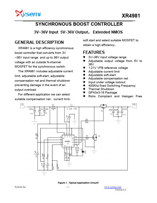
XR4981___________________________________________________________________________________________________________________ __XySemi Inc - 1 - SYNCHRONOUS BOOST CONTROLLER3V~36V Input 5V~36V Output , Extended NMOSGENERAL DESCRIPTIONXR4981 is a high efficiency synchronous boost controller that converts from 3V ~36V input range and up to 36V output voltage with an outside N-channel MOSFET for the synchronous switch. The XR4981 includes adjustable current limit, adjustable soft-start, adjustable compensation net and thermal shutdown preventing damage in the event of an output overload.For different application we can select suitable compensation net 、current limit 、soft start and select suitable MOSFET to obtain a high efficiency 。
FEATURES● 3V~36V input voltage range● Adjustable output voltage from 5V to36V● 1.21V VFB reference voltage ● Adjustable current limit ● Adjustable soft-start● Adjustable compensation net ● Input under voltage lockout● 400Khz fixed Switching Frequency ● Thermal Shutdown ● QFN3x3-16 Package● Rohs Compliant and Halogen FreeFigure 1. Typical Application Circuit1Figure 2. Typical Application Circuit2(Special for Single Li-Battery Input) APPLICATIONS●Power Bank●QC 2.0 Device●Type C USB Device●Power Amplify Device●Portable Class D Device●5V/9V/12V BUS Power SupplyTypical application for input and output:Input Voltage(V) Output Voltage(V) /Output Current(A) schematic3.3~4.35 5V/5A 9V/3A 12V/2A 14.8V/2A 20V/1.5A Circuit25 9V/4A 12V/3A 14.8V/2A 20V/1.5A Circuit16~8.4 9V/5A 12V/3A 14.8V/2.5A 20V/2A Circuit112~16.8 19V/4A 24V4A 20V/5.5A Circuit1ORDERING INFORMATIONPART NUMBER TEMP RANGESWICHINGFREQUENCYOUTPUTVOLTAGE (V)PACKAGE PINSXR4981 -40°C to 85°C 400KHZ ADJ QFN3x3 16 PIN CONFIGURATIONFigure 2. PIN Configuration (TOP View)PIN DESCRIPTIONPIN NUMBERPINNAMEPIN DESCRIPTION1 VCC Controller inside power logic Power Supply,inside LDO output pin,Must be closelydecoupled to GND with a 22uF MLCC capacitor.2 AVIN Controller Power Supply,inside LDO input pin., Connect this pin with input voltage.Must be closely decoupled to GND with a 1uF MLCC capacitor.3 VISP Input current sense pin1-Positive side4 VISN Input current sense pin1-Negative side5 COMP Loop compensation pin. Connect a RC network across this pin and ground to stabilize the control loop.6 PGOOD Power good indicator. Open drain output, pull low when the output < 90% or >110% of regulation voltage, high impendence otherwise.7 EN Enable Input. Pull high to turn on the IC. Do not let this pin float.8 FB Feedback pin. Connect to the center of resistor voltage divider to program the output voltage: VOUT=1.2V×(R1/R2+1), please place this network close to FB pin9 AGND Analog ground10 SS Soft-start setting pin, Select 10nF~100nF Css to set different soft-start time11 OC Input current setting pin. Connect a resistor Roc from this pin to AGND to program output current limitation threshold. For Example,10A~12A current limit by 100K12 BS Boot-Strap pin. Supply Rectified FET’s gate driver. Decouple this pin to LX with 0.1uFceramic cap .Please select Low VF schottky Diode.13 SW Switching Pin. Connect an inductor from power input to LX pin. Please select low Rdson & Big Enough Id & Isat inductor.14 SDRV High Side Power NMOS gate driver pin, Connect this pin to the gate of the high side synchronous rectifier N-channel MOSFET.15 PGND Power Ground16 MDRV LOW Side Power NMOS gate driver pin, Connect this pin to the gate of the low side N-channel MOSFETEPAD EPAD GND and Thermal Pad, Please connect with mass metal plane for good heat dissipationABSOLUTE MAXIMUM RATINGS(Note: Do not exceed these limits to prevent damage to the device. Exposure to absolute maximum rating conditions for long periods may affect device reliability.)PARAMETER VALUE UNIT AVIN、VISP、VISN、BS、SW、EN 40V V SDRV SW+6 V Other Pins 6V V Operating Ambient Temperature -40 to 85 °C Maximum Junction Temperature 150 °C Storage Temperature -55 to 150 °C Lead Temperature (Soldering, 10 sec) 300 °CELECTRICAL CHARACTERISTICS(V IN = 3.6V, T A= 25 C unless otherwise specified)PARAMETER SYMBOL TEST CONDITIONS MIN TYP MAX UNIT Input Voltage Range V IN 3 36 V Inside LDO output VCC Vin>=5V 4.2 V Boost output voltage range Vout 5 40 V UVLO Threshold V UVLO V HYSTERESIS =100mV 2.7 VOperating Supply CurrentI SUPPLY V FB =1.5V,EN=Vin=3.6V, I Load =0 70µAShutdown Supply Current V EN =0V, V IN =3.6V 10 Regulated FeedbackVoltageV FB 1.18 1.21 1.24 V Peak inductor Current limit(N-MOSFET current limit)Ilim Roc=100K & Rs=3mohm 12.5 A Oscillator Frequency F OSC 0.32 0.4 0.48 MHz Enable Threshold V IN = 2.3V to 5.5V 0.3 1 1.5 V Enable Leakage Current -0.1 0.1 µA Soft Start Time Tss Css=100nF Io=2A 300 msFunctional Block DiagramControl Logic-+Soft StartvrefEA-Current Sesneslope++ICMP4.2V LDO OSCVCCVINVISP VISNVOCCOMPSSFBGNDMDRVSWSDRVBSENPower GoodPGENCONTROLLER CIRCUITThe XR4981 is a constant-frequency ,PWM control , current mode boost controller. In normal operation, the external Main MOSFET is turned on each cycle when the oscillator gives an on-state. and then turned off when the main comparator -ICMP give an off state. The peak inductor current is controlled by the “COMP ” pin, which is the output of the error amplifier EA. The EA compares the signal VFB pin which is the feedback of VOUT , with the internal bandgap reference voltage 1.21V.. Peak inductor current is sensed by a resistor which is connected series with inductor. The inductor current is determined by the output of EA. A slope compensation is added because of the PWM control method. When the load current increases, it causes decrease in VFB, which in turn causes the output of EA increases until the average inductor current matches the new load current.OUTPUT VOLTAGE PROGRAMMINGThe output voltage is set by a resistive divider according to the following equation:Typically we suggest R10=10K or 12K and then determine R9 from the above equation 。
运放——精选推荐
运放可更换运放是Titanium HD的卖点之⼀,玩家可以根据⾃⼰的⾳⾊喜好更换对应兼容的运算放⼤器。
但我们⼀直并不喜欢这种设计,它多少反映了⼚商对⾳⾊的不⾃信,另外,使⽤插座⽐焊接更容易造成接触不良。
这张声卡的原配运放⼗分⾼档,JRC2114D应该是作为滤波和电流电压转换⽤途,⽽LME49710⽤于运算放⼤,这是⼀颗极低失真和极低噪声的芯⽚,其理论失真度(THD+N)可以低达0.00003%,这在业界属于最顶级⽔平。
LME49710和LME49713是国半的两款顶级单运放,49710是电压反馈型运放,49713是电流反馈型运放。
这两个运放的参数⾮常优秀,代表了⽬前模拟集成器件的最⾼⽔准。
49710的数据:FeaturesEasily drives 600 loadsOptimized for superior audio signal fidelityOutput short circuit protectionPSRR and CMRR exceed 120dB (typ)SOIC, DIP, TO-99 metal can packagesKey Specification ■Power Supply V oltage Range ±2.5V to ±17V■THD+N (A V = 1, VOUT = 3VRMS, fIN = 1kHz)RL = 2k? 0.00003% (typ)RL = 600? 0.00003% (typ)■Input Noise Density 2.5nV/ √^Hz (typ)■Slew Rate ±20V/µs (typ)■Gain Bandwidth Product 55MHz (typ)■Open Loop Gain (RL = 600?) 140dB (typ)■Input Bias Current 7nA (typ)■Input Offset V oltage 0.05mV (typ)■DC Gain Linearity Error 0.000009%General Description The LME49710 is part of the ultra-low distortion, low noise, high slew rate operational amplifier series optimized and fully specified for high performance, high fidelity applications.49713的数据:FeaturesEasily drives 150 loadsOptimized for superior audio signal fidelityOutput short circuit protection102dB (typ) PSRR and 88dB (typ) CMRRSOIC High Performance and Metal can packagesKey Specification ■Power Supply V oltage Range ±5V to ±18V■THD+N(A V = 1, RL = 100?, VOUT = 3VRMS,f = 1kHz) 0.0006% (typ)■THD+N(A V = 1, RL = 600?, VOUT = 1.4VRMS,f = 1kHz) 0.00008% (typ)■Input Noise Density 1.9nV/ √^Hz (typ)■Slew Rate ±1900V/µs (typ)■Bandwidth(A V = –1, RL= 2k?, RF = 1.2k?) 132MHz (typ)■Input Bias Current 1.8µA (typ)■Input Offset V oltage 0.05mV (typ)General Description The LME49713 is an ultra-low distortion, low noise, ultra high slew rate current feedback operational amplifier optimized and fully specified for high performance, high fidelity applications.【名称】发烧级⾳频运放【型号】LM49710HA(⾦封)【⼚商】NS国家半导体公司【产地】美国【规格】TO-99⾦属封装【成⾊】全新原装进⼝正品,质量上乘。
主流发烧运放IC的介绍

主流发烧运放IC的介绍兼评七款电压反馈型双运放运算放大器是运用得非常广泛的一种线性集成电路。
而且种类繁多,在运用方面不但可对微弱信号进行放大,还可做为反相、电压跟随器,可对电信号做加减法运算,所以被称为运算放大器。
不但其他地方应用广泛,在音响方面也使用得最多。
例如前级放大、缓冲,耳机放大器除了有部分使用分立元件,电子管外,绝大部分使用的还是集成运算放大器。
而有时候还会用到稳压电路上,制作高精度的稳压滤波电路。
各种运放由于其内部结构的不同,产生的失真成分也不同,所以音色特点也有一定的区别。
本来我们追求的是高保真,运放应该是失真最低,能真实还原音乐,没有个性的最好。
但是由于要配合其他音响部件如数码音源、后级功放管等如果偏干、偏冷则可搭配音色细腻温暖型的运放,而太过阴柔、偏软的则可搭配音色较冷艳、亮丽的运放,做到与整机配合,取长补短的最佳效果。
所以说并不是选择越贵的运放得到的效果就一定越好,搭配很重要,达到听感上最好才算达到目的。
如果是应用在低电压的模拟滤波电路中,还要选择对低电压工作性能良好的运放种类。
市面上的运放种类不下五六百种,GBW带宽在5M以上的也有三百多种,最高的已达300MHZ,转换速率在5V/us以上的也不下几百种,最高达3000V/us。
以上介绍的几种被音响发烧友们炒得火热的,其实还有大量未被大家熟知的上乘佳品可供选择,大家不必局限于以上几种。
一种运放型号的封装也可分为金封、陶封和塑封,一般来说金封、陶封的质量较好,塑封的品质稍差。
利益的驱使,什么都有假货,运放也不例外,市面上的假货不少,如果想便宜捡好货,那就要慧眼识珠了,不太在行的在购买时就要注意,宁可多花一块几毛,也要到信誉较好的商家去买。
低档运放JRC4558。
这种运放是低档机器使用得最多的。
现在被认为超级烂,因为它的声音过于明亮,毛刺感强,所以比起其他的音响用运放来说是最差劲的一种。
不过它在我国暂时应用得还是比较多的,很多的四、五百元的功放还是选择使用它,因为考虑到成本问题和实际能出的效果,没必要选择质量超过5532以上的运放。
LME49810中文资料
Supply Voltage |V+| + |V-| Differential Input Voltage Common Mode Input Range Power Dissipation (Note 3) ESD Susceptibility (Note 4) ESD Susceptibility (Note 5) Junction Temperature (TJMAX) (Note 9) Soldering Information
20216772源自2LME49810
元器件交易网 Connection Diagram
TB Package
Top View
20216702
Order Number LME49810TB
See NS Package Number TB15A
N = National Logo
Open Loop Gain Output Voltage Swing
VCM = 0V, VO = 0V, IO = 0A VCM = 0V, VO = 0V, IO = 0A No Load, BW = 30kHz VOUT = 30VRMS, f = 1kHz f = DC f = 1kHz, VIN = 1mVRMS THD+N = 0.05%, f = 1kHz
3
元器件交易网
LME49810
FIGURE 2. LME49810 Simplified Schematic
20216708
4
LME49810
元器件交易网
Absolute Maximum Ratings (Notes 1, 2)
LME49810 200V Audio Power Amplifier Driver with Baker Clamp
LME49810中文资料
200
nA (max)
110
105
dB (min)
VCLIP
Baker Clamp Clipping Voltage
Clip Output Source pin Sink pin
97.2 –96.4
95.5 –95.5
V (max) V (min)
VBC
Baker Clamp Flag Output Voltage IFLAG = 4.7mA
Байду номын сангаас
VBA
Bias P&M Pin Open Voltage
BiasP - BiasM
IBIAS
Bias Adjust Function Current
0.4
V
10
V
2.8
mA
5
LME49810
元器件交易网
Note 1: All voltages are measured with respect to the GND pin unless otherwise specified. Note 2: Absolute Maximum Ratings indicate limits beyond which damage to the device may occur. Operating Ratings indicate conditions for which the device is functional but do not guarantee specific performance limits. Electrical Characteristics state DC and AC electrical specifications under particular test conditions which guarantee specific performance limits. This assumes that the device is within the Operating Ratings. Specifications are not guaranteed for parameters where no limit is given, however, the typical value is a good indication of device performance. Note 3: The maximum power dissipation must be derated at elevated temperatures and is dictated by TJMAX, θJC, and the ambient temperature, TA. The maximum allowable power dissipation is PDMAX = (TJMAX - TA) / θJC or the number given in Absolute Maximum Ratings, whichever is lower. For the LME49810, TJMAX = 150° C and the typical θJC is 4°C/W. Refer to the Thermal Considerations section for more information. Note 4: Human body model, 100pF discharged through a 1.5kΩ resistor. Note 5: Machine Model, 220pF - 240pF discharged through all pins. Note 6: Typicals are measured at +25°C and represent the parametric norm. Note 7: Limits are guaranteed to National's AOQL (Average Outgoing Quality Level). Note 8: Datasheet min/max specification limits are guaranteed by design, test, or statistical analysis. Note 9: The maximum operating junction temperature is 150°C. Note 10: Data taken with Bandwidth = 30kHz, AV = 29dB, CC = 10pF, and TA = 25°C except where specified.
【超级透】LME49810推场管K1058J162单声道功放成品板

【超级透】LME49810推场管K1058J162单声道功放成品板核⼼元件:K1058/J162 是⼀对让⼈⾮常着魔的⾳响专⽤对管,不仅仅因为它是场管,有着电⼦管的特性,它能够刻画出如丝绸般润滑的细腻的中⾼⾳,在⼈声、管弦⽅⾯所刻画出来的⾳⾊让⼈绕梁三⽇不绝。
核⼼元件:采⽤国半的发烧级推动元件LM49810TB,具有失真低、功率⼤、推动⼒⼤(57mA)、不⽤配对,轻松获得优秀的⾳质。
本板线路:采⽤LME49810TB直推2对K1058/J162的线路,线路简洁,稳定,声⾳⼗分通透。
直流伺服:采⽤直流伺服电路,减少了输⼊、退耦电容对⾳质的影响,延伸了⾼低频,线路异常稳定,声⾳⾮常通透;甲类电流:在变压器、散热器温度允许的情况下,尽量调⼤静态电流吧,感受甲类功放(温暖、通透、控制⼒好)的动⼈魅⼒!此板调试⽅法:此板只有⼀个可调多圈电位器,⽤于调节功率管的静态电流(甲类电流)。
此板焊接完成后,在通电前,先将可调电位器逆时针旋转到头(此时静态电流为0)。
进⾏通电试⾳,确认放⾳⽆问题后,再缓慢沿顺时针调节电位器,同时检测0.22欧电阻电压(如44mV 时,静态为200mA,⽤mV档测量功率管的E对输出也可以),将静态电流调节到需要值。
注意:因为温度反馈的作⽤,随着散热器的温度上升,静态电流会被拉下来⼀点,需要多次测试、调试。
推荐电压:关于甲类的调整,本功放板末级静态电流可以调整,获得理想的⾳质,使⽤本店的配套的散热器:在±48供电时,推荐将每对管调整到100mA;在±35V供电时,推荐将静态电流调整到150mA。
输出功率:根据电源电压的不同、喇叭阻抗的不同,输出功率20-200w;印板尺⼨:148*55mm;安装功率管后:148*70mm;2mm厚、70um铜箔;中点电压:1mV左右;信噪⽐:105dB,噪⾳电平:0.3mV;配套散热器:253*80*50mm,0.8kg,每对管可以调到150mA;。
LME控制器说明书

CC1N7101en Building Technologies燃烧控制器用于单段或双段式中小容量(最高350KW)燃气燃烧器的间歇式操作。
LME…系列控制器适用于将燃烧控制器配套使用OEM 工厂。
应用,特征LME…用于单段或双段的燃气燃烧器在启动和间歇式运行期间的监测控制。
火焰监控通过离子棒或火焰探测器QRA 及辅助设备AGQ3或使用蓝火焰探测器QRC 。
根据外壳的尺寸规格,LME...与LGB 和LMG 是一样的燃烧控制器(参考«型号总览»)燃烧控制器符合EN 298标准强排风燃烧器符合EN 676标准欠压检测用空气压力开关监测启动和运行时的空气压力便捷的远程复位多种颜色显示错误状态和操作状态的信息限定次数的重复循环精确的控制顺序是由于使用数字信号处理方式24小时连续运行后须停机一次7101燃烧控制器LME...应用特征注意事项∙所有行为(装备,安装和售后服务等)必须由专业人员来完成。
∙在LME…的连接区域改变任何接线之前,使控制器完全与主电源绝缘(两极断开)。
∙给燃烧控制器的接线柱提供充足的保护,确保控制器不受电击的危险。
∙检查空气压力开关连接线是否短路(接线端3,6和11)∙按锁定复位按钮为手动(所需压力不超过10N)不允许使用其他任何工具或是尖状物体。
∙坠落或撞击会影响安全功能。
这样的控制器不能运作,即使外观没有任何损失。
∙每次的工作都应该这样执行(装备,安装,售后服务等),检查确认接线的有序确保安全«调试注意事项»技术注意事项∙当连接伺服电机时,燃烧控制器执行机构没有位置反馈信号。
∙当连接伺服电机时,必须按EN676标准执行。
∙伺服电机的运行时间必须与燃烧控制程序匹配。
必须对燃烧器和执行器一起进行安全检查。
∙当用LME…系列替换LGB或者LMG时,AGQ1或AGQ2…必须由AGQ3…来代替。
MIL-STD-498学习笔记

A forgotten military standard that saves weeks of work(by providing free project management templates)Nobody loves to write documentation, but with age and experience, IT project managers usually come to accept that it can be useful sometimes, even necessary. In healthy doses.Now, if you're doing small to medium software projects, the US military might not be your usual place to turn to for inspiration. But in one case, back in '94, they did create something truly wonder-, power-, and useful. (Then they've thrown it away and replaced it with a complex and much less useful hybrid IEEE and ISO monster. But there's an interesting twist -- more on that later.)This gem is inspirationally called "MIL-STD-498".It was created to fix the problems with an older standard (the DOD 2167A, if you need to know), for example its insistence on using the waterfall model, or requiring huge demonstration events that stopped development for weeks. (People unofficially called those "dog & pony shows".)MIL-STD-498 can help you if you are a developer dealing with clients, but also if you're a project manager dealing with suppliers. I personally had used it in both situations.By the end of this article, you'll be proficient enough in it to brag about it. And to know how to use it for various purposes when the need arises the next time.So, why is MIL-STD-498 so cool and unique?1. It's in the public domain, so you're free to use it. Unlike IEEE or ISO standards, which you'd have to buy.Like the Internet RFCs, it's out there. Actually, it's right here (zip download).I had an assistant convert the templates (called "DIDs", Data Item Descriptions) to friendly clean HTML (with nested header levels and without messy formatting), so you can easily use it with any word processor. The original Word-97 files even MS Office doesn't seem to read correctly anymore.2. It's completely self-sufficient. It invokes no other standard. It'sstand-alone.Some standards get entangled with others by invoking various other standards, requiring you to include, import (and often buy) documents that belong to those other standards, not only resulting in a chaotic mess, but also making it hard to initially estimate how big the work of documentation will be.3. It is essentially a collection of document templates. And not only a table of contents (although that already would be a great free project management template), but also "help" paragraphs explaining what to include, how to approach the topic, what to reference, etc.Even if you're not doing full-blown documentation, these project management templates ("DIDs") are useful as checklists.4. It's compatible with the latest. You might be thinking, "ok, but still, an outdated standard? Why should I even care?" But, you have to know that the MIL-STD-498 later got "civilized" as J-STD-016, which became part of the current IEEE/EIA 12207 (which also includes, but is not the same as ISO 12207, just to demonstrate how chaotic it can get in the world of standards). So, basically, if you work with MIL-STD-498, you're creating documents that perfectly fit into the modern 12207! (Which, by the way, doesn't have document templates for you, even if you buy it. Just saying.)5. It's quite flexible. The creators of the standard have understood that projects come in various shapes, sizes, and colors. So, the MIL-STD-498can officially be customized to the project. They call it "tailoring", andthey've even written a full guide on how to do it officially. But in most cases, if you're not a DoD supplier, just feel free to leave out the parts you feel are not important for your project (for example, the part about how the item is supposed to work when there are enemy explosions nearby.)Also, it allows the use of electronic tools instead of written word, when appropriate. Its thinking is that the point is that you have the stuff, not that it must be written in a word processor.6. It supports multiple program strategies. It clearly says that there are three ways of doing projects: "Grand design" (also known as, waterfall), "Incremental" (which most Agile projects do), and even "Evolutionary" (which includes exploratory projects like prototypes).So, how does one actually use it?Well, there's the 344 pages long "Application and ReferenceGuide" (Part1, Part2), and the 99-page strong "Overview and Tailoring Guide". Or, you can start using the templates (the "DIDs") right away just after reading this short introduction from me.(I'm listing the documents in the order they usually get written. Of course, certain projects might be different. Or you just need one template to document one aspect -- feel free to.)Request For Quotation phaseOCD - Operational Concept Description. This describes in the client's language what the project is about, what is wrong with thecurrent situation, how will the system improve it. If you're adeveloper, it's best used as a checklist for questioning the client aboutthe project details; if you're a project manager, use it as a template towrite a very good description of your planned project for thesuppliers.(Pro tip: As a purchaser, you get lower prices if your description is well thought out, and not vague. The developers' biggest risk factor isactually you: They know how they can program, but they don't know how difficult you are. A good, concise project description shows that you have already had put ample thought into the project, which is a good sign, and they don't have to pad the estimates just in case you turn out to be the Client From Hell Who Orders A Car But Actually Needs A Submarine.)∙SDP - Software Development Plan. It just describes the very basics of how the development will happen: languages, tools, source control, trouble ticketing, change management, testing, validation, phases,timetable, etc. It's best used as a checklist of things that should go intoa contract.These two are usually enough for an initial ballpark price quoting phase. There's one more that has to be done before contracting - just so it's clear for everyone what is the acceptance criteria:∙STP - Software Test Plan. It describes in general how and where the testing (especially the acceptance testing) will happen, without goinginto details on individual tests. (Those come later in the unfortunatelynamed STD document.)Now when the project is about to start, proceed to the next ones:System design phase∙SSS - System/Subsystem Specification and SRS - Software Requirement Specification. There can be only one SSS, but if needed, there can be an SRS for each Subsystem. (I usually only do thissub-document thing if the different subsystems are the responsibilities of different suppliers.) The SSS and SRS are basically the same anddiffer only in minor wording -- in theory, the SSS might containhardware descriptions too, while the SRS can only describe software. The SSS (and maybe SRSes) is how one describes the architecture of the system. This is best done in cooperation (in "Joint Application Design", or JAD sessions, if you want a military-sounding buzzword) between the client and the developer. Use it as a template.∙IRS - Interface Requirement Specification. Only needed if the system will connect to one or more external systems. Best used as achecklist of what to collect from (usually) third parties. (One canrarely dictate the format of third party documentation.)The SSS (or SRS) and the IRS should contain enough information that the software development can actually be done. It should start now. The following documents are to be done during the development: Development phase∙SSDD - System/Subsystem Design Description (or SDD - Software Design Description) and IDD - Interface Design Description. These describe the evolving, and in the end the final design of the systemand the subsystems and the interfaces. These are basicallycounterparts with the Specifications:SSS - SSDDSRS - SDDIRS - IDDThe templates that end in "S" (as in Specification) are supposedly written (or at least, the information is given) by the customer; while the ones ending in "DD" (as in "Design Description"), are written by the developer.This might sound nitpicking at first, but actually, it's very important, because MIL-STD-498 does away with the usual thinking that the customer says "what" to do, and the developer decides "how" to do things. It says that if it's in the Specifications then the developer must comply with it, doesn't matter if it's a "what" or a "how"; on the other hand, if something is not in the specification (be that a "what" or "how"), then it's up to the developer, but should be documented in the "DD"-s. See how beautiful the separation of responsibilities is?This separation fits both knowledgeable and less experienced customers, since they can specify as much or as less as they wish, or can.∙DBDD - Database Design Description. Just what it sounds. Actually, this one is often better done with a "create table, create index, etc"SQL script or with one of the fancy database design tools than in atext editor. (That's what MIL-STD-498's spirit says: Don't you dare to copy the SQL into the documentation just to make it look thick. Justgive me the file.)∙STD - Software Test Description. This well-named template describes the information missing from the STP (the Test Plan) --namely, the individual tests. Best used as a checklist, the teststhemselves can usually be best described in a spreadsheet format. Tests should cover every important functionality of the system, and also don't forget that tests are needed for two purposes: 1) to check functionality, and 2) to test against possible attacks.In my experience, tests are best written both by the customer and the developer separately, and then merged together. (There will be overlaps that need to be reconciled, but there will also be interesting differences in approach.) Also, I find it best if test descriptions are written once at thebeginning of the development, then retouched and expanded again as the end is nearing (and in between if the development is long enough or is separated to phases).Test descriptions are a very good way to find hidden requirements. Don't miss the opportunity, early in the process.Testing phase∙STR - Software Test Report. This is basically the output of doing the STDs according to the STP. Best read once for scraping ideas, andactually done by adding check marks and notes to a copy of the STDspreadsheet.Manuals∙SUM - Software user manual. Very good template. Use it. (And don't forget, it's best to document by user functions, not by features.But this is just my advice, it's not in the standard.) Can be omitted ifthere is no user interface.∙SIOM - Software Input/Output Manual. It's best used as a template for documenting APIs. Omit if there is no API.∙SCOM - Software Center Operator Manual. A template to document the operation of the system. It's to be done if someone else will do the hosting.Delivery phase∙SPS - Software Product Specification. Best used as a checklist of things expected to be delivered.∙SVD - Software Version Description. This is basically a "change log"template. Use when delivering changes to a system already inoperation.Rarely used DIDsTemplates that are rarely used -- at least in my line of work:∙STrP - Software Transition Plan. It describes how to transfer the support functions to the customer's internal support agency. It wouldbasically be a knowledge base for user support personnel.∙COM - Computer Operation Manual. Well, unless you're developinga whole new computer. In that case, you should totally use this one.∙CPM - Computer Programming Manual. I guess it's a useful starting point if your software has it's own programming language.FSM - Firmware Support Manual. I suppose it's useful for embedded systems. Which I haven't done lately.ConclusionIf you are a military supplier, or intent on doing this the "perfect" way, then definitely read the two big manuals. And the Appendices. And tailor the documents by the book.But just by having the above information in your head (or in your browser), and having access to these templates, I'll say that you're already 85% of the way. Most "normal" project managers, even with relatively big projects, will never need to know more about MIL-STD-498 than this. Insert it into your own process.I wish that you use this little gem with success - and start to hate doing documentation just a little less. :)。
基于PCM2702E和LME49830的音频功率放大器设计与实现

基于PCM2702E和LME49830的音频功率放大器设计与实现叶军;李景;洛藏尖措【摘要】为改善和提高普通声卡的品质,使用USB接口DAC(数模转换器)芯片PCM2702E完成对数据流中音频信号的还原,并采用专为驱动MOSFET管而设计的高性能音频驱动LME49830芯片,设计出高品质新型音频多媒体功放.该功放能显著减少由于音源和功率放大器之间距离较远所导致信号传输过程引入的干扰.【期刊名称】《青海大学学报(自然科学版)》【年(卷),期】2015(033)004【总页数】6页(P46-50,58)【关键词】PCM2702E;LME49830;音频功率放大器【作者】叶军;李景;洛藏尖措【作者单位】青海大学机械工程学院,青海西宁810016;青海大学机械工程学院,青海西宁810016;青海大学机械工程学院,青海西宁810016【正文语种】中文【中图分类】TN99多媒体功放在使用时若放大器距离电脑较远,容易由音频功放输入信号线引入干扰、并造成音频信号的较大衰减,而且多数电脑是采用集成声卡,音质也并不理想,为解决上述问题,利用PCM2702E和LME49830设计并制作出新的音频多媒体功率放大器,该多媒体功率放大器信号输入直联电脑USB口,基于USB传输的特性,电脑和多媒体功放可分隔较长的距离,且避免了音频信号的损失和外界的干扰。
整个功率放大器包含USB接口的DAC转换、音频功率放大和电源三部分组成,组成框图见图1。
PCM2702E为美国TI公司属下的BB(Burr-Brown)公司生产的USB接口DAC芯片,28条引脚,典型封装形式为SSOP-28,内部具有USB接口控制芯片及16位D/A转换功能。
其典型特性是:信噪比高(典型值105dB);总谐波失真小(THD+N为0.002%);动态范围大(为100dB);分离度好(为103 dB);符合USB1.0接口标准,因为PCM2702E上市时间较早,比起后续产品来说,在音频性能上来看,如DNR(动态范围)和SNR(信噪比)指标,性能是最好的(较之后来的升级版本),本设计主要是利用其音频DAC(数模转换器)功能,因此最合适。
用LME49810制作高性能功率放大器

用LME49810制作高性能功率放大器距离第一篇文章发表已有好长一段时间了(因女儿出生),现在我的小女儿已经1岁多,所以我的制作和研究又可以继续了。
在第一篇文章中,曾推荐了一款采用国半高性能驱动芯片LME49810的功放。
这块芯片的性能已经在不同负载下测量过。
得出的建议是,驱动级必须要为输出级提供足够的驱动电流,输出级由此选择ON(安森美)的NJL3281D/1302D。
这对管子由于内含偏置二极管,具有同时实现热补偿功能,因此传统的Vbe倍乘器就可以取消了。
在本文中主要介绍电源部分的设计及如何借助仪器监测功放的THD(总谐波失真加噪声)指标、如何用频谱分析的方法来调整功放的静态电流至最佳值,最后部分是功放的性能测试结果,其中包括了THD测试、IMD测试和方波测试。
一、电源设计本功放设计在8Ω 负载上至少有120W输出。
这样,每个输出级晶体管将分担1.9A的有效值电流(本功放使用了两对管子)。
从NJL3281D/1302D的资料可知,其V ce的线性工作区的最小值是5V,这样要满足满功率输出,电源电压(V+、V-)至少要达到49V,其计算如下:P out=120(W)=I 2out×8=V 2out /8Iout= 120/8= 15≈3.87(A)V +=V - =120×8× 2+5≈49(V)电源部分电路如图1所示。
V+ 及V-在满功率输出状态起码要49V,加上变压器的损耗和纹波,我们选择了未经稳压的±55V,此时变压器次级电压为交流39V。
桥堆中的二极管在大电流状态下会有约1V的压降,同时我们也必须考虑市电电压的变化,这样,就需要一个双0~42V次级电压绕组的变压器,且次级必须要能提供4A的有效值电流。
如果你希望在4Ω负载上得到翻倍的输出功率,就必须要有一个满足8A电流的变压器!光有大变压器还不行,大水塘式电容也是必要的。
我使用了两个桥堆(B1、B2)来组成双桥全波整流,这样DC 0V也包含在整流回路中。
2.7W双声道立体音频放大器
2.7W双声道立体音频放大器概述4985SD是一款双通道桥接的音频功率放大器,在5V电源电压4Ω负载时,可提供2.7W的功率。
具有低功耗关断模式和过温保护功能。
在电路启动时,具有缓冲及防抖动功能。
功能特点l缓冲及防抖动l过温保护l低功耗关断模式l PO为1% THD+N, VDD = 5VRL=4Ω 2.2W(typ)RL=8Ω 1.4W(typ)l PO为10% THD+N, VDD = 5VRL=4Ω 2.7W(typ)RL=8Ω 1.7W(typ)l PO为1% THD+N, VDD = 4VRL=4Ω 1.4W(typ)RL=8Ω0.88W(typ)l关断电流0.04μA(typ)l工作电压范围 2.7V~5.5Vl封装方式:DIP16(4985SD)用途l手机、PDA、MP4、PMPl手提电脑l桌面音响设备l多媒体显示器管脚排列图管脚说明功能框图功能说明桥接参数说明4985SD由两对运算放大器组成双通道(通道A和通道B)立体声放大器。
外接反馈电阻R2,R4和输入电阻R1,R3决定了放大器A(-out)和B(-out)的闭环增益,同时内建20K电阻使放大器A的(+out)和B的(-out)端的增益为1。
4985SD所驱动的负载接在两放大器的输出端-OUTA和+OUTA之间。
放大器A的(-out)端就是放大器A的(+out)端的输入端,这就使两个输出端产生的信号有180°的相位差,利用这个相位差,桥接模式下的增益为:A VD=2*(Rf/Ri)或者A VD=2*(R2/R1)桥接模式比单端模式更有优势。
在桥接模式下,差分输出使增益翻倍,它的输出功率是相同情况下单端模式的4倍。
桥接模式的另一个优势是在负载上没有直流电压。
输出信号由通道A和B偏置在VDD/2。
所以它无需在单端模式下的耦合电容。
在单端输出模式下,如果不使用输出耦合电容,就会在负载上产生一个VDD/2的直流偏置电压,这就会增加芯片的功耗并对负载造成永久性的损害。
基于LME49830芯片音频放大器

基于LME49830芯片音频放大器一个非常简单的高效率功放电路可设计的LME49830高保真音频功率放大器输入级为满足日益苛刻的消费电子和专业音频应用而设计的的。
LME49830芯片是能够驾驶超过300瓦的输出阶段,成为单端8Ω负载10%的高线和20%的余量供应规例的存在。
LME49830芯片包括内部热关断电路,激活时,LME49830芯片的管芯温度超过150 ° C。
LME49830芯片具有静音功能,静音输入驱动信号放大器的输出和力量处于静止状态。
,随着偏置电压范围高达16V LME49830芯片可用于驱动MOSFET输出级使用的MOSFET广泛的选择,也是LME49830芯片支持宽工作电源电压范围从± 20V到± 100V,允许使用成本低,不稳定的电源供应。
这音频功率放大器电路是一个每边MOSFET输出阶段的LME4983直接驱动两个设备。
当是从一个双60伏供电电路运行此音频功率音频放大器能够提供一个335瓦,THD 4欧姆负载的10%总谐波失真0.1%或430瓦的输出功率,如果你将使用一个8欧姆负载,最大输出功率将175瓦的总谐波失真0.1%或230瓦,THD10%,但是你可以看到在电路原理,高保真音频功率放大器需要很少的外部元件,并会提供一个单声道音频放大器。
如果你需要一个立体声音频放大器电路中,您将需要兴建两个电路,这音频放大器的电源电压的限制,是基于东芝2SK1530/2SJ201 MOSFET 200V VDSS。
建议应用到该功率放大器的最大电源电压小于80伏此模块的功耗大约为4欧姆负载和60伏91瓦8欧姆负载和60伏电源和182瓦电源功耗等级,因为这个模块必须热sinked使用一个4英寸的挤出机的散热片,并额外取决于空气的流动,以减少热阻,可以安装一个风扇。
- 1、下载文档前请自行甄别文档内容的完整性,平台不提供额外的编辑、内容补充、找答案等附加服务。
- 2、"仅部分预览"的文档,不可在线预览部分如存在完整性等问题,可反馈申请退款(可完整预览的文档不适用该条件!)。
- 3、如文档侵犯您的权益,请联系客服反馈,我们会尽快为您处理(人工客服工作时间:9:00-18:30)。
随着输出的电平增加,被提取进入“Zobel”网络的电流也随之会上升。因此,在任 何条件下输出网络中元件的额定参数都必须足够。
3. 可减轻交流耦合 RC 网络的噪声。
负反馈系数 功率放大器的负反馈设置可为系统带来较高的稳定性和线性度。采用负反馈可防止 放大器直流偏移电压出现饱和。一般来说,当放大器在高频工作时会出现相位位 移,而较大的负反馈系数可减轻在高频时的不稳定性和振荡。
在离散的放大器系统中,高反馈系数将会引起很差的瞬态响应或高频不稳定性。然 而,LME49810 拥有一个较高的开环增益,因此它的闭环增益误差和电源纹波抑制 会较小,可以最大化电路中的负反馈,从而提高系统的线性度。通常,建议采用 30dB 至 40dB 的电压增益。 通过设置输入电阻和反馈电阻,很容易就可以设定出负反馈系数
静音控制、静音 输出偏置及输出级 输出偏置电路
LME49810 有两根用来设定偏置的专用引脚(BIASP 和 BIASM),可以提供一定的输 出偏置电流。可变电阻器 R pot 可用来调节输出级的偏置电流,将 R pot+Rb1 的电 阻降低可以提高偏置电压。 倍增器 QMULT 用来补偿偏置电压以防止双极输出晶 体管出现热漂移。 QMULT 必须与输出晶体管连接在相同的散热器上。当温度上升时,Vbe 会减小以 降低偏置电压,较高的偏置电流可减少输出的交越失真,但同时会消耗较大的电 流。
等效RE Amp
RE
Rload
此外,RE电阻是开环输出阻抗的主要成份。闭环输出阻抗由开环输出阻抗和负反 馈系数来定义,其关系如下:
Rout _ closeloop
=
Rout _ openloop Negative _ Feedback _
factor
例如:平均开环输出阻抗为200mΩ,负反馈系数为29dB或28倍。这样,我们便可 预期闭环输出阻抗约为7mΩ。在一般情况下,闭环阻抗最好比扬声器系统的阻抗 低很多,以便尽量提升线性度。
例如:假设输出摆幅为 20 Vrms,那“Zobel” 网络在 20kHz 下应会消耗 248mA 或 0.62W。可是,为了确保组件能在一段短时间的高功率和高频下工作,因此“Zobel” 组件的功率额定一般都建议为 3W 到 5W。
“Zobel”网络的另一个功能是保护放大器的输出以免受到扬声器线圈内电感所影 响。
例如: MN2488 和 MP1620 为了提高输出级的稳定性,负极端和正极端的电流放大必须匹配。 输出级晶体管的电流匹配 对于并行晶体管配置来说,必须确定中等功率晶体管的驱动能力。中等功率晶体管 的输出电流(Ic)必须大于高功率晶体管的最小驱动电流(Ib)以免在中等功率晶体管级 上出现过载。 例子:KSC2073(中等功率级)
静音 MUTE 引脚是由流进的电流量所控制。方法是用一个电阻器将参考电压连接到 MUTE 引脚以控制电流的大小。从 50uA 到 100uA 为 “PLAY”模式,而低于 50uA 的为 “MUTE”模式。
静音电流可从以下的算式计算出来:
数式 2
可是,建议不要让流进 MUTE 引脚的电流超出 200 uA。
TO-247 15 引线封装
LME49810 最适合使用在高端的消费和专业级音频应用中,包括有源录音室监视 器、超重低音扬声器、音频/视频接收器、商用扩音系统、非原厂音响、专业级混 音器,分布式音频和吉他放大器等。此外,这款芯片也适用于各类高电压及低失真 要求的工业用音频系统。
主要规格 宽阔的工作电压范围
图 6. 50mA 的偏置电流 图 10. 500mA 的偏置电流 输出电晶体 音频功率放大器中最常见的输出级是下图所示的射极跟随器。它通常都被称为双射 极跟随器或达林顿复合晶体管对。其中第一个跟随器会作为一个输出器件的驱动 器。
射极跟随器的大信号线性度主要取决于负载的大小。随着负载增加(即负载电阻减 少),输出电流亦同时会增加。受RE(射极电阻)和位于高电流密度的beta 滚降的影 响,BJT电流增益会减少。
当然,LME49810 的输入偏置电流很低,对于一般的应用来说,出现在输出的偏移 电压可以忽略。
例如,LME49810 的典型偏置电流为 100nA,而输入阻抗失配为 1KΩ。 Voffset = I bias × Rmis−match = 100nA×1闭环增益的放大器
利用高电压音频驱动器设计高性能音频放大器的准则与思考
作者: 美国国家半导体资深产品应用工程师 Kenneth Lee
引言: 无论是外观、款式、系统控制还是音质,音频放大器产品越来越先进。经验丰富的 电子工程师正采用不同的电路来设计其理想的音频放大器。
现在许多传统高功率音频放大器的每通道输出功率在 100 瓦以上,并且大多采用离 散的电路元件。因此,为了确保输出的稳定性和音效,工程师需要花很大精力对高 保真音频放大器进行匹配和调节。
Voutput−offset = 0.1mV × 30 = 3mV 由于 LME49810 的输入偏置电流很低,出现在输出的偏移电压在一般应用下都不
会很明显。
假如希望进一步减少输出的偏移电压,便需要降低反馈和输入信号路径上的阻抗。 这样就可以减少由输入偏置电流失衡引起的偏移。,但前提是必须确保前端有足够 的驱动能力。 一般来说,通常采用的的音频输入设计有两种:交流或直流耦合输入。根据应用要 求来选用合适的输入设计: 交流耦合输入的优点: 1. 来自前置放大器、滤波器级或编解码器级的放大器输入直流偏移一般都是零。 2. 无需在放大器中加入任何的直流伺服电路来防止直流故障。 直流耦合输入的优点: 1. 无需使用大尺寸和昂贵的交流耦合电容器。 2. 不会出现由交流耦合电容器所产生的低频失真。
数式 1
补偿 放大器的补偿是用来调节开环增益和相位性能,以便当反馈被关闭时能把系统稳定 下来。一般来说,要获得较高的稳定性补偿越大越好。可是,补偿越大,音频芯片 的带宽和压摆率就越低,而较低的压摆率会使系统产生出较柔和的音频特性,相反 较高的压摆率则可产生较清晰和真实的音频特性。
LME49810 的密勒补偿是通过在 “Comp” 和 “BiasM” 引脚之间加插一个电容器来实 现的。
集电极-基极电压、集电极-射极电压
从上表可看到,中等功率晶体管的基极和集极引脚在工作期间的电压约为 Vee 或 Vcc 的两倍。因此在选择晶体管时,必须确保晶体管的电压额定够高。
电阻器RE 在高功率的音频放大器应用中,输出晶体管的匹配性、电流平衡和保护对于功率放 大器的线性度来说非常重要。 这里建议采用射极负反馈电阻器RE来改善输出晶体管的匹配性和电流平衡能力。 因此,我们建议在实际的高功率音频放大器应用中加入这种电阻。 然而,将RE与输出晶体管串联在一起会降低放大器的线性度。电阻RE是交越失真 的主要失真来源。当输出电晶体的一端关闭而另一端开启时便会出现这种失真。 因此,必须优化RE值并且尽可能的将RE值维持在较低水平,这样可以降低对非线性 度的影响。
因此,改善交越失真的最有效方法便是减少RE的电阻。对于相同数值的RE,一个 并行形式的输出可降低用来改善线性度的整体RE电阻值。同时,假如每一个级的 RE都较大,那便可为输出晶体管带来更佳的匹配性和电流平衡。
此外,RE也关系到输出的功率损耗。对于一个相同的RE,较大的输出电流会导致 较大的功率损耗。RE的值取决于并联输出晶体管的数量和扬声器的负载。 一般来说,可采用有足够功率的 0.1 到 0.5Ω电阻器。 RE 的消耗功率可从这条数式计算出来:RxI²=W Eg. 0.1Ohm x 5A² =2.5W
产品应用: 美国国家半导体向来擅长开发创新性的音频技术,并且将突破性的技术应用于新产 品。最新推出的高电压的音频驱动器 LME49810,可以协助设计人员更容易的开发 出高性能音频系统。
高性能音频放大器 LME49810 可提供一个 200V 的峰峰值输出电压摆幅,并可驱动 不同类型的输出级。这款设计简洁的集成电路可为音频系统提供更精简的设计,更 高的稳定性和一致性。因此,可以极大的减少系统研发和生产时的离散组件匹配及 调节工作。换句话说,LM49810 能够提升效率和降低生产成本。
例子:. FJL3415 (高功率级)
集电极电流、基极电流
输出晶体管的电压范围 采用输出晶体管首先要考虑到其电压范围,这样可确保系统的稳定性,并防止系统 受到任何形式的损坏。 VCBO 和 VCEO 电压的最大范围必须大于电源电压的轨到轨范围。对于一个有+/100V 电压供应的放大器,晶体管的电压额定应该高一点以保证它能够在规定以内 正常地运作。
±20V 到±100V
压摆率 输出驱动电流 电源纹波抑制比 (f=DC) 总谐波失真及噪声(f=1KHz)
50V/µs(典型值) 600mA(典型值) 110dB(典型值) 0.0007(典型值)
利用 LME49810 设计音频放大器的建议 采用美国国家半导体的音频驱动器来设计高品质音频系统的方法有很多。在此,仅 列举若干重要的建议。
由于一个扬声器的真实负载阻抗比起一个简单的并行电阻器和电容器要复杂得多。 受到串联在一起的放大器输出阻抗、电缆阻抗及电感的影响,一个真实的扬声器的 频率响应会出呈现不平稳的特性。这种现象可能导致高频不稳定性。
在放大器的输出串联一个小线圈电感器会增加稳定性。这种做法可以将放大器与关 联电容器隔离,并且不会在音频的频率下引致明显的损耗。
输入级 输入级设计是放大器最关键的一环。通过来自反馈的信号进行相减,输入级会产生 一个误差信号,然后把这个误差信号驱动到输出。该误差信号通常很小,足以为放 大器提供足够的线性度。
LME49810 是一款双极输入放大器,其输入阻抗的匹配性相当重要。受来自正输入 端口和负输入端口的偏置电流的影响,输入阻抗的失配会导致输入偏移电压。该输 入偏移电压将按照闭环增益放大,在输出端出现。