养老保险单位缴费可按基数12%跨省转移
NuMicro N9H30系列开发板用户手册说明书
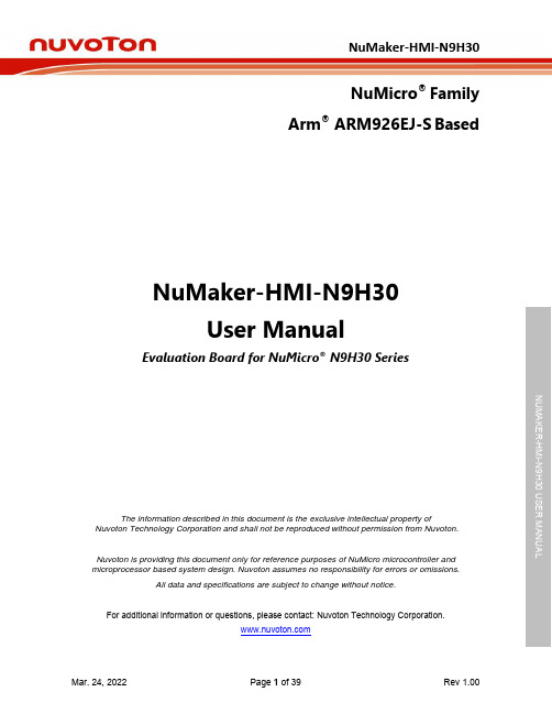
NuMicro®FamilyArm® ARM926EJ-S BasedNuMaker-HMI-N9H30User ManualEvaluation Board for NuMicro® N9H30 SeriesNUMAKER-HMI-N9H30 USER MANUALThe information described in this document is the exclusive intellectual property ofNuvoton Technology Corporation and shall not be reproduced without permission from Nuvoton.Nuvoton is providing this document only for reference purposes of NuMicro microcontroller andmicroprocessor based system design. Nuvoton assumes no responsibility for errors or omissions.All data and specifications are subject to change without notice.For additional information or questions, please contact: Nuvoton Technology Corporation.Table of Contents1OVERVIEW (5)1.1Features (7)1.1.1NuMaker-N9H30 Main Board Features (7)1.1.2NuDesign-TFT-LCD7 Extension Board Features (7)1.2Supporting Resources (8)2NUMAKER-HMI-N9H30 HARDWARE CONFIGURATION (9)2.1NuMaker-N9H30 Board - Front View (9)2.2NuMaker-N9H30 Board - Rear View (14)2.3NuDesign-TFT-LCD7 - Front View (20)2.4NuDesign-TFT-LCD7 - Rear View (21)2.5NuMaker-N9H30 and NuDesign-TFT-LCD7 PCB Placement (22)3NUMAKER-N9H30 AND NUDESIGN-TFT-LCD7 SCHEMATICS (24)3.1NuMaker-N9H30 - GPIO List Circuit (24)3.2NuMaker-N9H30 - System Block Circuit (25)3.3NuMaker-N9H30 - Power Circuit (26)3.4NuMaker-N9H30 - N9H30F61IEC Circuit (27)3.5NuMaker-N9H30 - Setting, ICE, RS-232_0, Key Circuit (28)NUMAKER-HMI-N9H30 USER MANUAL3.6NuMaker-N9H30 - Memory Circuit (29)3.7NuMaker-N9H30 - I2S, I2C_0, RS-485_6 Circuit (30)3.8NuMaker-N9H30 - RS-232_2 Circuit (31)3.9NuMaker-N9H30 - LCD Circuit (32)3.10NuMaker-N9H30 - CMOS Sensor, I2C_1, CAN_0 Circuit (33)3.11NuMaker-N9H30 - RMII_0_PF Circuit (34)3.12NuMaker-N9H30 - RMII_1_PE Circuit (35)3.13NuMaker-N9H30 - USB Circuit (36)3.14NuDesign-TFT-LCD7 - TFT-LCD7 Circuit (37)4REVISION HISTORY (38)List of FiguresFigure 1-1 Front View of NuMaker-HMI-N9H30 Evaluation Board (5)Figure 1-2 Rear View of NuMaker-HMI-N9H30 Evaluation Board (6)Figure 2-1 Front View of NuMaker-N9H30 Board (9)Figure 2-2 Rear View of NuMaker-N9H30 Board (14)Figure 2-3 Front View of NuDesign-TFT-LCD7 Board (20)Figure 2-4 Rear View of NuDesign-TFT-LCD7 Board (21)Figure 2-5 Front View of NuMaker-N9H30 PCB Placement (22)Figure 2-6 Rear View of NuMaker-N9H30 PCB Placement (22)Figure 2-7 Front View of NuDesign-TFT-LCD7 PCB Placement (23)Figure 2-8 Rear View of NuDesign-TFT-LCD7 PCB Placement (23)Figure 3-1 GPIO List Circuit (24)Figure 3-2 System Block Circuit (25)Figure 3-3 Power Circuit (26)Figure 3-4 N9H30F61IEC Circuit (27)Figure 3-5 Setting, ICE, RS-232_0, Key Circuit (28)Figure 3-6 Memory Circuit (29)Figure 3-7 I2S, I2C_0, RS-486_6 Circuit (30)Figure 3-8 RS-232_2 Circuit (31)Figure 3-9 LCD Circuit (32)NUMAKER-HMI-N9H30 USER MANUAL Figure 3-10 CMOS Sensor, I2C_1, CAN_0 Circuit (33)Figure 3-11 RMII_0_PF Circuit (34)Figure 3-12 RMII_1_PE Circuit (35)Figure 3-13 USB Circuit (36)Figure 3-14 TFT-LCD7 Circuit (37)List of TablesTable 2-1 LCD Panel Combination Connector (CON8) Pin Function (11)Table 2-2 Three Sets of Indication LED Functions (12)Table 2-3 Six Sets of User SW, Key Matrix Functions (12)Table 2-4 CMOS Sensor Connector (CON10) Function (13)Table 2-5 JTAG ICE Interface (J2) Function (14)Table 2-6 Expand Port (CON7) Function (16)Table 2-7 UART0 (J3) Function (16)Table 2-8 UART2 (J6) Function (16)Table 2-9 RS-485_6 (SW6~8) Function (17)Table 2-10 Power on Setting (SW4) Function (17)Table 2-11 Power on Setting (S2) Function (17)Table 2-12 Power on Setting (S3) Function (17)Table 2-13 Power on Setting (S4) Function (17)Table 2-14 Power on Setting (S5) Function (17)Table 2-15 Power on Setting (S7/S6) Function (18)Table 2-16 Power on Setting (S9/S8) Function (18)Table 2-17 CMOS Sensor Connector (CON9) Function (19)Table 2-18 CAN_0 (SW9~10) Function (19)NUMAKER-HMI-N9H30 USER MANUAL1 OVERVIEWThe NuMaker-HMI-N9H30 is an evaluation board for GUI application development. The NuMaker-HMI-N9H30 consists of two parts: a NuMaker-N9H30 main board and a NuDesign-TFT-LCD7 extensionboard. The NuMaker-HMI-N9H30 is designed for project evaluation, prototype development andvalidation with HMI (Human Machine Interface) function.The NuMaker-HMI-N9H30 integrates touchscreen display, voice input/output, rich serial port serviceand I/O interface, providing multiple external storage methods.The NuDesign-TFT-LCD7 can be plugged into the main board via the DIN_32x2 extension connector.The NuDesign-TFT-LCD7 includes one 7” LCD which the resolution is 800x480 with RGB-24bits andembedded the 4-wires resistive type touch panel.Figure 1-1 Front View of NuMaker-HMI-N9H30 Evaluation BoardNUMAKER-HMI-N9H30 USER MANUAL Figure 1-2 Rear View of NuMaker-HMI-N9H30 Evaluation Board1.1 Features1.1.1 NuMaker-N9H30 Main Board Features●N9H30F61IEC chip: LQFP216 pin MCP package with DDR (64 MB)●SPI Flash using W25Q256JVEQ (32 MB) booting with quad mode or storage memory●NAND Flash using W29N01HVSINA (128 MB) booting or storage memory●One Micro-SD/TF card slot served either as a SD memory card for data storage or SDIO(Wi-Fi) device●Two sets of COM ports:–One DB9 RS-232 port with UART_0 used 75C3232E transceiver chip can be servedfor function debug and system development.–One DB9 RS-232 port with UART_2 used 75C3232E transceiver chip for userapplication●22 GPIO expansion ports, including seven sets of UART functions●JTAG interface provided for software development●Microphone input and Earphone/Speaker output with 24-bit stereo audio codec(NAU88C22) for I2S interfaces●Six sets of user-configurable push button keys●Three sets of LEDs for status indication●Provides SN65HVD230 transceiver chip for CAN bus communication●Provides MAX3485 transceiver chip for RS-485 device connection●One buzzer device for program applicationNUMAKER-HMI-N9H30 USER MANUAL●Two sets of RJ45 ports with Ethernet 10/100 Mbps MAC used IP101GR PHY chip●USB_0 that can be used as Device/HOST and USB_1 that can be used as HOSTsupports pen drives, keyboards, mouse and printers●Provides over-voltage and over current protection used APL3211A chip●Retain RTC battery socket for CR2032 type and ADC0 detect battery voltage●System power could be supplied by DC-5V adaptor or USB VBUS1.1.2 NuDesign-TFT-LCD7 Extension Board Features●7” resolution 800x480 4-wire resistive touch panel for 24-bits RGB888 interface●DIN_32x2 extension connector1.2 Supporting ResourcesFor sample codes and introduction about NuMaker-N9H30, please refer to N9H30 BSP:https:///products/gui-solution/gui-platform/numaker-hmi-n9h30/?group=Software&tab=2Visit NuForum for further discussion about the NuMaker-HMI-N9H30:/viewforum.php?f=31 NUMAKER-HMI-N9H30 USER MANUALNUMAKER-HMI-N9H30 USER MANUAL2 NUMAKER-HMI-N9H30 HARDWARE CONFIGURATION2.1 NuMaker-N9H30 Board - Front View Combination Connector (CON8)6 set User SWs (K1~6)3set Indication LEDs (LED1~3)Power Supply Switch (SW_POWER1)Audio Codec(U10)Microphone(M1)NAND Flash(U9)RS-232 Transceiver(U6, U12)RS-485 Transceiver(U11)CAN Transceiver (U13)Figure 2-1 Front View of NuMaker-N9H30 BoardFigure 2-1 shows the main components and connectors from the front side of NuMaker-N9H30 board. The following lists components and connectors from the front view:NuMaker-N9H30 board and NuDesign-TFT-LCD7 board combination connector (CON8). This panel connector supports 4-/5-wire resistive touch or capacitance touch panel for 24-bits RGB888 interface.Connector GPIO pin of N9H30 FunctionCON8.1 - Power 3.3VCON8.2 - Power 3.3VCON8.3 GPD7 LCD_CSCON8.4 GPH3 LCD_BLENCON8.5 GPG9 LCD_DENCON8.7 GPG7 LCD_HSYNCCON8.8 GPG6 LCD_CLKCON8.9 GPD15 LCD_D23(R7)CON8.10 GPD14 LCD_D22(R6)CON8.11 GPD13 LCD_D21(R5)CON8.12 GPD12 LCD_D20(R4)CON8.13 GPD11 LCD_D19(R3)CON8.14 GPD10 LCD_D18(R2)CON8.15 GPD9 LCD_D17(R1)CON8.16 GPD8 LCD_D16(R0)CON8.17 GPA15 LCD_D15(G7)CON8.18 GPA14 LCD_D14(G6)CON8.19 GPA13 LCD_D13(G5)CON8.20 GPA12 LCD_D12(G4)CON8.21 GPA11 LCD_D11(G3)CON8.22 GPA10 LCD_D10(G2)CON8.23 GPA9 LCD_D9(G1) NUMAKER-HMI-N9H30 USER MANUALCON8.24 GPA8 LCD_D8(G0)CON8.25 GPA7 LCD_D7(B7)CON8.26 GPA6 LCD_D6(B6)CON8.27 GPA5 LCD_D5(B5)CON8.28 GPA4 LCD_D4(B4)CON8.29 GPA3 LCD_D3(B3)CON8.30 GPA2 LCD_D2(B2)CON8.31 GPA1 LCD_D1(B1)CON8.32 GPA0 LCD_D0(B0)CON8.33 - -CON8.34 - -CON8.35 - -CON8.36 - -CON8.37 GPB2 LCD_PWMCON8.39 - VSSCON8.40 - VSSCON8.41 ADC7 XPCON8.42 ADC3 VsenCON8.43 ADC6 XMCON8.44 ADC4 YMCON8.45 - -CON8.46 ADC5 YPCON8.47 - VSSCON8.48 - VSSCON8.49 GPG0 I2C0_CCON8.50 GPG1 I2C0_DCON8.51 GPG5 TOUCH_INTCON8.52 - -CON8.53 - -CON8.54 - -CON8.55 - -NUMAKER-HMI-N9H30 USER MANUAL CON8.56 - -CON8.57 - -CON8.58 - -CON8.59 - VSSCON8.60 - VSSCON8.61 - -CON8.62 - -CON8.63 - Power 5VCON8.64 - Power 5VTable 2-1 LCD Panel Combination Connector (CON8) Pin Function●Power supply switch (SW_POWER1): System will be powered on if the SW_POWER1button is pressed●Three sets of indication LEDs:LED Color DescriptionsLED1 Red The system power will beterminated and LED1 lightingwhen the input voltage exceeds5.7V or the current exceeds 2A.LED2 Green Power normal state.LED3 Green Controlled by GPH2 pin Table 2-2 Three Sets of Indication LED Functions●Six sets of user SW, Key Matrix for user definitionKey GPIO pin of N9H30 FunctionK1 GPF10 Row0 GPB4 Col0K2 GPF10 Row0 GPB5 Col1K3 GPE15 Row1 GPB4 Col0K4 GPE15 Row1 GPB5 Col1K5 GPE14 Row2 GPB4 Col0K6GPE14 Row2GPB5 Col1 Table 2-3 Six Sets of User SW, Key Matrix Functions●NAND Flash (128 MB) with Winbond W29N01HVS1NA (U9)●Microphone (M1): Through Nuvoton NAU88C22 chip sound input●Audio CODEC chip (U10): Nuvoton NAU88C22 chip connected to N9H30 using I2Sinterface–SW6/SW7/SW8: 1-2 short for RS-485_6 function and connected to 2P terminal (CON5and J5)–SW6/SW7/SW8: 2-3 short for I2S function and connected to NAU88C22 (U10).●CMOS Sensor connector (CON10, SW9~10)–SW9~10: 1-2 short for CAN_0 function and connected to 2P terminal (CON11)–SW9~10: 2-3 short for CMOS sensor function and connected to CMOS sensorconnector (CON10)Connector GPIO pin of N9H30 FunctionCON10.1 - VSSCON10.2 - VSSNUMAKER-HMI-N9H30 USER MANUALCON10.3 - Power 3.3VCON10.4 - Power 3.3VCON10.5 - -CON10.6 - -CON10.7 GPI4 S_PCLKCON10.8 GPI3 S_CLKCON10.9 GPI8 S_D0CON10.10 GPI9 S_D1CON10.11 GPI10 S_D2CON10.12 GPI11 S_D3CON10.13 GPI12 S_D4CON10.14 GPI13 S_D5CON10.15 GPI14 S_D6CON10.16 GPI15 S_D7CON10.17 GPI6 S_VSYNCCON10.18 GPI5 S_HSYNCCON10.19 GPI0 S_PWDNNUMAKER-HMI-N9H30 USER MANUAL CON10.20 GPI7 S_nRSTCON10.21 GPG2 I2C1_CCON10.22 GPG3 I2C1_DCON10.23 - VSSCON10.24 - VSSTable 2-4 CMOS Sensor Connector (CON10) FunctionNUMAKER-HMI-N9H30 USER MANUAL2.2NuMaker-N9H30 Board - Rear View5V In (CON1)RS-232 DB9 (CON2,CON6)Expand Port (CON7)Speaker Output (J4)Earphone Output (CON4)Buzzer (BZ1)System ResetSW (SW5)SPI Flash (U7,U8)JTAG ICE (J2)Power ProtectionIC (U1)N9H30F61IEC (U5)Micro SD Slot (CON3)RJ45 (CON12, CON13)USB1 HOST (CON15)USB0 Device/Host (CON14)CAN_0 Terminal (CON11)CMOS Sensor Connector (CON9)Power On Setting(SW4, S2~S9)RS-485_6 Terminal (CON5)RTC Battery(BT1)RMII PHY (U14,U16)Figure 2-2 Rear View of NuMaker-N9H30 BoardFigure 2-2 shows the main components and connectors from the rear side of NuMaker-N9H30 board. The following lists components and connectors from the rear view:● +5V In (CON1): Power adaptor 5V input ●JTAG ICE interface (J2) ConnectorGPIO pin of N9H30Function J2.1 - Power 3.3V J2.2 GPJ4 nTRST J2.3 GPJ2 TDI J2.4 GPJ1 TMS J2.5 GPJ0 TCK J2.6 - VSS J2.7 GPJ3 TD0 J2.8-RESETTable 2-5 JTAG ICE Interface (J2) Function●SPI Flash (32 MB) with Winbond W25Q256JVEQ (U7); only one (U7 or U8) SPI Flashcan be used●System Reset (SW5): System will be reset if the SW5 button is pressed●Buzzer (BZ1): Control by GPB3 pin of N9H30●Speaker output (J4): Through the NAU88C22 chip sound output●Earphone output (CON4): Through the NAU88C22 chip sound output●Expand port for user use (CON7):Connector GPIO pin of N9H30 FunctionCON7.1 - Power 3.3VCON7.2 - Power 3.3VCON7.3 GPE12 UART3_TXDCON7.4 GPH4 UART1_TXDCON7.5 GPE13 UART3_RXDCON7.6 GPH5 UART1_RXDCON7.7 GPB0 UART5_TXDCON7.8 GPH6 UART1_RTSCON7.9 GPB1 UART5_RXDCON7.10 GPH7 UART1_CTSCON7.11 GPI1 UART7_TXDNUMAKER-HMI-N9H30 USER MANUAL CON7.12 GPH8 UART4_TXDCON7.13 GPI2 UART7_RXDCON7.14 GPH9 UART4_RXDCON7.15 - -CON7.16 GPH10 UART4_RTSCON7.17 - -CON7.18 GPH11 UART4_CTSCON7.19 - VSSCON7.20 - VSSCON7.21 GPB12 UART10_TXDCON7.22 GPH12 UART8_TXDCON7.23 GPB13 UART10_RXDCON7.24 GPH13 UART8_RXDCON7.25 GPB14 UART10_RTSCON7.26 GPH14 UART8_RTSCON7.27 GPB15 UART10_CTSCON7.28 GPH15 UART8_CTSCON7.29 - Power 5VCON7.30 - Power 5VTable 2-6 Expand Port (CON7) Function●UART0 selection (CON2, J3):–RS-232_0 function and connected to DB9 female (CON2) for debug message output.–GPE0/GPE1 connected to 2P terminal (J3).Connector GPIO pin of N9H30 Function J3.1 GPE1 UART0_RXDJ3.2 GPE0 UART0_TXDTable 2-7 UART0 (J3) Function●UART2 selection (CON6, J6):–RS-232_2 function and connected to DB9 female (CON6) for debug message output –GPF11~14 connected to 4P terminal (J6)Connector GPIO pin of N9H30 Function J6.1 GPF11 UART2_TXDJ6.2 GPF12 UART2_RXDJ6.3 GPF13 UART2_RTSJ6.4 GPF14 UART2_CTSTable 2-8 UART2 (J6) Function●RS-485_6 selection (CON5, J5, SW6~8):–SW6~8: 1-2 short for RS-485_6 function and connected to 2P terminal (CON5 and J5) –SW6~8: 2-3 short for I2S function and connected to NAU88C22 (U10)Connector GPIO pin of N9H30 FunctionSW6:1-2 shortGPG11 RS-485_6_DISW6:2-3 short I2S_DOSW7:1-2 shortGPG12 RS-485_6_ROSW7:2-3 short I2S_DISW8:1-2 shortGPG13 RS-485_6_ENBSW8:2-3 short I2S_BCLKNUMAKER-HMI-N9H30 USER MANUALTable 2-9 RS-485_6 (SW6~8) FunctionPower on setting (SW4, S2~9).SW State FunctionSW4.2/SW4.1 ON/ON Boot from USB SW4.2/SW4.1 ON/OFF Boot from eMMC SW4.2/SW4.1 OFF/ON Boot from NAND Flash SW4.2/SW4.1 OFF/OFF Boot from SPI Flash Table 2-10 Power on Setting (SW4) FunctionSW State FunctionS2 Short System clock from 12MHzcrystalS2 Open System clock from UPLL output Table 2-11 Power on Setting (S2) FunctionSW State FunctionS3 Short Watchdog Timer OFFS3 Open Watchdog Timer ON Table 2-12 Power on Setting (S3) FunctionSW State FunctionS4 Short GPJ[4:0] used as GPIO pinS4Open GPJ[4:0] used as JTAG ICEinterfaceTable 2-13 Power on Setting (S4) FunctionSW State FunctionS5 Short UART0 debug message ONS5 Open UART0 debug message OFFTable 2-14 Power on Setting (S5) FunctionSW State FunctionS7/S6 Short/Short NAND Flash page size 2KBS7/S6 Short/Open NAND Flash page size 4KBS7/S6 Open/Short NAND Flash page size 8KBNUMAKER-HMI-N9H30 USER MANUALS7/S6 Open/Open IgnoreTable 2-15 Power on Setting (S7/S6) FunctionSW State FunctionS9/S8 Short/Short NAND Flash ECC type BCH T12S9/S8 Short/Open NAND Flash ECC type BCH T15S9/S8 Open/Short NAND Flash ECC type BCH T24S9/S8 Open/Open IgnoreTable 2-16 Power on Setting (S9/S8) FunctionCMOS Sensor connector (CON9, SW9~10)–SW9~10: 1-2 short for CAN_0 function and connected to 2P terminal (CON11).–SW9~10: 2-3 short for CMOS sensor function and connected to CMOS sensorconnector (CON9).Connector GPIO pin of N9H30 FunctionCON9.1 - VSSCON9.2 - VSSCON9.3 - Power 3.3VCON9.4 - Power 3.3V NUMAKER-HMI-N9H30 USER MANUALCON9.5 - -CON9.6 - -CON9.7 GPI4 S_PCLKCON9.8 GPI3 S_CLKCON9.9 GPI8 S_D0CON9.10 GPI9 S_D1CON9.11 GPI10 S_D2CON9.12 GPI11 S_D3CON9.13 GPI12 S_D4CON9.14 GPI13 S_D5CON9.15 GPI14 S_D6CON9.16 GPI15 S_D7CON9.17 GPI6 S_VSYNCCON9.18 GPI5 S_HSYNCCON9.19 GPI0 S_PWDNCON9.20 GPI7 S_nRSTCON9.21 GPG2 I2C1_CCON9.22 GPG3 I2C1_DCON9.23 - VSSCON9.24 - VSSTable 2-17 CMOS Sensor Connector (CON9) Function●CAN_0 Selection (CON11, SW9~10):–SW9~10: 1-2 short for CAN_0 function and connected to 2P terminal (CON11) –SW9~10: 2-3 short for CMOS sensor function and connected to CMOS sensor connector (CON9, CON10)SW GPIO pin of N9H30 FunctionSW9:1-2 shortGPI3 CAN_0_RXDSW9:2-3 short S_CLKSW10:1-2 shortGPI4 CAN_0_TXDSW10:2-3 short S_PCLKTable 2-18 CAN_0 (SW9~10) Function●USB0 Device/HOST Micro-AB connector (CON14), where CON14 pin4 ID=1 is Device,ID=0 is HOST●USB1 for USB HOST with Type-A connector (CON15)●RJ45_0 connector with LED indicator (CON12), RMII PHY with IP101GR (U14)●RJ45_1 connector with LED indicator (CON13), RMII PHY with IP101GR (U16)●Micro-SD/TF card slot (CON3)●SOC CPU: Nuvoton N9H30F61IEC (U5)●Battery power for RTC 3.3V powered (BT1, J1), can detect voltage by ADC0●RTC power has 3 sources:–Share with 3.3V I/O power–Battery socket for CR2032 (BT1)–External connector (J1)●Board version 2.1NUMAKER-HMI-N9H30 USER MANUAL2.3 NuDesign-TFT-LCD7 -Front ViewFigure 2-3 Front View of NuDesign-TFT-LCD7 BoardFigure 2-3 shows the main components and connectors from the Front side of NuDesign-TFT-LCD7board.7” resolution 800x480 4-W resistive touch panel for 24-bits RGB888 interface2.4 NuDesign-TFT-LCD7 -Rear ViewFigure 2-4 Rear View of NuDesign-TFT-LCD7 BoardFigure 2-4 shows the main components and connectors from the rear side of NuDesign-TFT-LCD7board.NuMaker-N9H30 and NuDesign-TFT-LCD7 combination connector (CON1).NUMAKER-HMI-N9H30 USER MANUAL 2.5 NuMaker-N9H30 and NuDesign-TFT-LCD7 PCB PlacementFigure 2-5 Front View of NuMaker-N9H30 PCB PlacementFigure 2-6 Rear View of NuMaker-N9H30 PCB PlacementNUMAKER-HMI-N9H30 USER MANUALFigure 2-7 Front View of NuDesign-TFT-LCD7 PCB PlacementFigure 2-8 Rear View of NuDesign-TFT-LCD7 PCB Placement3 NUMAKER-N9H30 AND NUDESIGN-TFT-LCD7 SCHEMATICS3.1 NuMaker-N9H30 - GPIO List CircuitFigure 3-1 shows the N9H30F61IEC GPIO list circuit.Figure 3-1 GPIO List Circuit NUMAKER-HMI-N9H30 USER MANUAL3.2 NuMaker-N9H30 - System Block CircuitFigure 3-2 shows the System Block Circuit.NUMAKER-HMI-N9H30 USER MANUALFigure 3-2 System Block Circuit3.3 NuMaker-N9H30 - Power CircuitFigure 3-3 shows the Power Circuit.NUMAKER-HMI-N9H30 USER MANUALFigure 3-3 Power Circuit3.4 NuMaker-N9H30 - N9H30F61IEC CircuitFigure 3-4 shows the N9H30F61IEC Circuit.Figure 3-4 N9H30F61IEC CircuitNUMAKER-HMI-N9H30 USER MANUAL3.5 NuMaker-N9H30 - Setting, ICE, RS-232_0, Key CircuitFigure 3-5 shows the Setting, ICE, RS-232_0, Key Circuit.NUMAKER-HMI-N9H30 USER MANUALFigure 3-5 Setting, ICE, RS-232_0, Key Circuit3.6 NuMaker-N9H30 - Memory CircuitFigure 3-6 shows the Memory Circuit.NUMAKER-HMI-N9H30 USER MANUALFigure 3-6 Memory Circuit3.7 NuMaker-N9H30 - I2S, I2C_0, RS-485_6 CircuitFigure 3-7 shows the I2S, I2C_0, RS-486_6 Circuit.NUMAKER-HMI-N9H30 USER MANUALFigure 3-7 I2S, I2C_0, RS-486_6 Circuit3.8 NuMaker-N9H30 - RS-232_2 CircuitFigure 3-8 shows the RS-232_2 Circuit.NUMAKER-HMI-N9H30 USER MANUALFigure 3-8 RS-232_2 Circuit3.9 NuMaker-N9H30 - LCD CircuitFigure 3-9 shows the LCD Circuit.NUMAKER-HMI-N9H30 USER MANUALFigure 3-9 LCD Circuit3.10 NuMaker-N9H30 - CMOS Sensor, I2C_1, CAN_0 CircuitFigure 3-10 shows the CMOS Sensor,I2C_1, CAN_0 Circuit.NUMAKER-HMI-N9H30 USER MANUALFigure 3-10 CMOS Sensor, I2C_1, CAN_0 Circuit3.11 NuMaker-N9H30 - RMII_0_PF CircuitFigure 3-11 shows the RMII_0_RF Circuit.NUMAKER-HMI-N9H30 USER MANUALFigure 3-11 RMII_0_PF Circuit3.12 NuMaker-N9H30 - RMII_1_PE CircuitFigure 3-12 shows the RMII_1_PE Circuit.NUMAKER-HMI-N9H30 USER MANUALFigure 3-12 RMII_1_PE Circuit3.13 NuMaker-N9H30 - USB CircuitFigure 3-13 shows the USB Circuit.NUMAKER-HMI-N9H30 USER MANUALFigure 3-13 USB Circuit3.14 NuDesign-TFT-LCD7 - TFT-LCD7 CircuitFigure 3-14 shows the TFT-LCD7 Circuit.Figure 3-14 TFT-LCD7 CircuitNUMAKER-HMI-N9H30 USER MANUAL4 REVISION HISTORYDate Revision Description2022.03.24 1.00 Initial version NUMAKER-HMI-N9H30 USER MANUALNUMAKER-HMI-N9H30 USER MANUALImportant NoticeNuvoton Products are neither intended nor warranted for usage in systems or equipment, anymalfunction or failure of which may cause loss of human life, bodily injury or severe propertydamage. Such applications are deemed, “Insecure Usage”.Insecure usage includes, but is not limited to: equipment for surgical implementation, atomicenergy control instruments, airplane or spaceship instruments, the control or operation ofdynamic, brake or safety systems designed for vehicular use, traffic signal instruments, all typesof safety devices, and other applications intended to support or sustain life.All Insecure Usage shall be made at customer’s risk, and in the event that third parties lay claimsto Nuvoton as a result of customer’s Insecure Usage, custome r shall indemnify the damagesand liabilities thus incurred by Nuvoton.。
宽频pmu 49次谐波 相位问题
宽频pmu 49次谐波相位问题摘要:1.宽频PMU 的概念及其应用领域2.谐波和相位问题的定义及产生原因3.宽频PMU 49 次谐波相位问题的具体表现4.解决宽频PMU 49 次谐波相位问题的方法5.总结正文:一、宽频PMU 的概念及其应用领域宽频脉冲测量单元(PMU)是一种高精度的电力系统测量设备,能够实时测量电力系统中的电压、电流、频率等参数。
PMU 具有很高的采样频率和精度,可以准确地捕捉到电力系统中的高频谐波信号。
因此,宽频PMU 在电力系统的故障诊断、保护和控制等领域具有重要的应用价值。
二、谐波和相位问题的定义及产生原因谐波是指频率为基频整数倍的电压或电流分量。
在电力系统中,谐波会导致设备过热、绝缘老化、电力损耗等问题。
而相位问题是指电力系统中电压和电流之间的相位差,它影响电力系统的稳定性和设备的安全性。
三、宽频PMU 49 次谐波相位问题的具体表现在宽频PMU 的测量过程中,可能会出现49 次谐波相位问题。
具体表现为:在测量电压和电流的49 次谐波时,其相位差与理论值存在较大偏差。
这可能会导致电力系统中出现谐波共振现象,进而引发设备故障。
四、解决宽频PMU 49 次谐波相位问题的方法针对宽频PMU 49 次谐波相位问题,可以采取以下方法进行解决:1.校准方法:通过采集标准信号,对PMU 进行校准,使其测量结果更加准确。
2.滤波方法:采用数字滤波技术,对PMU 采集到的信号进行滤波处理,降低谐波干扰。
3.算法优化:通过改进相位测量算法,提高测量精度,降低谐波相位问题的影响。
五、总结宽频PMU 在电力系统中具有重要的应用价值,但49 次谐波相位问题是其在实际应用中可能遇到的问题。
MT-049
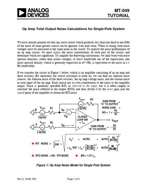
MT-049TUTORIALOp Amp Total Output Noise Calculations for Single-Pole SystemWe have already pointed out that any noise source which produces less than one third to one fifth of the noise of some greater source can be ignored, with little error. When so doing, both noise voltages must be measured at the same point in the circuit. To analyze the noise performance of an op amp circuit, we must assess the noise contributions of each part of the circuit, and determine which are significant. To simplify the following calculations, we shall work with noise spectral densities, rather than actual voltages, to leave bandwidth out of the expressions (the noise spectral density, which is generally expressed in nV/√Hz, is equivalent to the noise in a 1 Hz bandwidth).If we consider the circuit in Figure 1 below, which is an amplifier consisting of an op amp and three resistors (R3 represents the source resistance at node A), we can find six separate noise sources: the Johnson noise of the three resistors, the op amp voltage noise, and the current noise in each input of the op amp. Each source has its own contribution to the noise at the amplifier output. Noise is generally specified RTI, or referred to the input , but it is often simpler to calculate the noise referred to the output (RTO) and then divide it by the noise gain (not the signal gain) of the amplifier to obtain the RTI noise.V RTO NOISE = NG •RTI NOISEFigure 1: Op Amp Noise Model for Single Pole SystemBW = 1.57 f CLFigure 2 (below) is a detailed analysis of how each of the noise sources in Fig. 1 is reflected to the output of the op amp. Some further discussion regarding the effect of the current noise at the inverting input is warranted. This current, I N–, does not flow in R1, as might be expected—the negative feedback around the amplifier works to keep the potential at the inverting input unchanged, so that a current flowing from that pin is forced, by negative feedback, to flow in R2 only, resulting in a voltage at the output of I N– R2. We could equally well consider the voltage caused by I N– flowing in the parallel combination of R1 and R2 and then amplified by the noise gain of the amplifier, but the results are identical—only the calculations are more involved.NOISE SOURCE EXPRESSED ASA VOLTAGEJohnson noise in R3:√(4kTR3)Non-inverting input currentnoise flowing in R3:I N+R3Input voltage noise:V NJohnson noise in R1:√(4kTR1)Johnson noise in R2:√(4kTR2)Inverting input current noiseflowing in R2:I N–R2MULTIPLY BY THIS FACTOR TO REFER TO THE OP AMP OUTPUT Noise Gain = 1 + R2/R1Noise Gain = 1 + R2/R1Noise Gain = 1 + R2/R1–R2/R1 (Gain from input of R1to output)11Figure 2: Noise Sources Referred to the Output (RTO)Notice that the Johnson noise voltage associated with the three resistors has been included in the expressions of Fig. 2. All resistors have a Johnson noise of √(4kTBR), where k is Boltzmann's Constant (1.38×10⁻²³J/K), T is the absolute temperature, B is the bandwidth in Hz, and R is the resistance in Ω. A simple relationship which is easy to remember is that a 1000 Ω resistor generates a Johnson noise of 4 nV/√Hz at 25ºC.The analysis so far assumes a single-pole system where the feedback network is purely resistive and that the noise gain versus frequency is flat. This applies to most applications, but if the feedback network contains reactive elements (usually capacitors) the noise gain is not constant over the bandwidth of interest, and more complex techniques must be used to calculate the total noise. Second-order system noise considerations can be found in Tutorial MT-050.REFERENCES1.Hank Zumbahlen, Basic Linear Design, Analog Devices, 2006, ISBN: 0-915550-28-1. Also available asLinear Circuit Design Handbook, Elsevier-Newnes, 2008, ISBN-10: 0750687037, ISBN-13: 978-0750687034. Chapter 1.2.Walter G. Jung, Op Amp Applications, Analog Devices, 2002, ISBN 0-916550-26-5, Also available as OpAmp Applications Handbook, Elsevier/Newnes, 2005, ISBN 0-7506-7844-5. Chapter 1.Copyright 2009, Analog Devices, Inc. All rights reserved. Analog Devices assumes no responsibility for customer product design or the use or application of customers’ products or for any infringements of patents or rights of others which may result from Analog Devices assistance. All trademarks and logos are property of their respective holders. Information furnished by Analog Devices applications and development tools engineers is believed to be accurate and reliable, however no responsibility is assumed by Analog Devices regarding technical accuracy and topicality of the content provided in Analog Devices Tutorials.。
STMicroelectronics DfuSe USB设备固件升级用户手册说明书
UM0412User manual Getting started with DfuSe USB device firmware upgradeSTMicroelectronics extensionIntroductionThis document describes the demonstration user interface that was developed to illustrateuse of the STMicroelectronics device firmware upgrade library. A description of this library,including its application programming interface, is contained in the “DfuSe applicationprogramming interface” document and installed with the DfuSe software.July 2009Doc ID 13379 Rev 41/22Contents UM0412Contents1Getting started . . . . . . . . . . . . . . . . . . . . . . . . . . . . . . . . . . . . . . . . . . . . . . 51.1System requirements . . . . . . . . . . . . . . . . . . . . . . . . . . . . . . . . . . . . . . . . . 51.2Package contents . . . . . . . . . . . . . . . . . . . . . . . . . . . . . . . . . . . . . . . . . . . . 61.3DfuSe demonstration installation . . . . . . . . . . . . . . . . . . . . . . . . . . . . . . . . 61.3.1Software installation . . . . . . . . . . . . . . . . . . . . . . . . . . . . . . . . . . . . . . . . . 61.3.2Hardware installation . . . . . . . . . . . . . . . . . . . . . . . . . . . . . . . . . . . . . . . . 6 2DFU file . . . . . . . . . . . . . . . . . . . . . . . . . . . . . . . . . . . . . . . . . . . . . . . . . . . 123User interface description . . . . . . . . . . . . . . . . . . . . . . . . . . . . . . . . . . . 133.1DfuSe demonstration . . . . . . . . . . . . . . . . . . . . . . . . . . . . . . . . . . . . . . . . 133.2DFU file manager . . . . . . . . . . . . . . . . . . . . . . . . . . . . . . . . . . . . . . . . . . . 153.2.1“Want to do” dialog box . . . . . . . . . . . . . . . . . . . . . . . . . . . . . . . . . . . . . 153.2.2File generation dialog box . . . . . . . . . . . . . . . . . . . . . . . . . . . . . . . . . . . 163.2.3File extraction dialog box . . . . . . . . . . . . . . . . . . . . . . . . . . . . . . . . . . . . 174Step-by-step procedures . . . . . . . . . . . . . . . . . . . . . . . . . . . . . . . . . . . . 194.1DfuSe demonstration procedures . . . . . . . . . . . . . . . . . . . . . . . . . . . . . . . 194.1.1How to upload a DFU file . . . . . . . . . . . . . . . . . . . . . . . . . . . . . . . . . . . . 194.1.2How to download a DFU file . . . . . . . . . . . . . . . . . . . . . . . . . . . . . . . . . 194.2DFU file manager procedures . . . . . . . . . . . . . . . . . . . . . . . . . . . . . . . . . 204.2.1How to generate DFU files from S19/Hex/Bin files . . . . . . . . . . . . . . . . 204.2.2How to extract S19/Hex/Bin files from DFU files . . . . . . . . . . . . . . . . . . 20 5Revision history . . . . . . . . . . . . . . . . . . . . . . . . . . . . . . . . . . . . . . . . . . . 212/22 Doc ID 13379 Rev 4UM0412List of tables List of tablesTable 1.DfuSe demo dialog box description . . . . . . . . . . . . . . . . . . . . . . . . . . . . . . . . . . . . . . . . . . 14 Table 2.File generation dialog box description . . . . . . . . . . . . . . . . . . . . . . . . . . . . . . . . . . . . . . . . 16 Table 3.Multi bin injection dialog box description . . . . . . . . . . . . . . . . . . . . . . . . . . . . . . . . . . . . . . 17 Table 4.File extraction dialog box description . . . . . . . . . . . . . . . . . . . . . . . . . . . . . . . . . . . . . . . . . 18 Table 5.Document revision history . . . . . . . . . . . . . . . . . . . . . . . . . . . . . . . . . . . . . . . . . . . . . . . . . 21Doc ID 13379 Rev 43/22List of figures UM0412 List of figuresFigure 1.System properties dialog box. . . . . . . . . . . . . . . . . . . . . . . . . . . . . . . . . . . . . . . . . . . . . . . . 5 Figure 2.Selecting the installation location . . . . . . . . . . . . . . . . . . . . . . . . . . . . . . . . . . . . . . . . . . . . . 7 Figure 3.Driver selection option . . . . . . . . . . . . . . . . . . . . . . . . . . . . . . . . . . . . . . . . . . . . . . . . . . . . . 8 Figure 4.Driver selection. . . . . . . . . . . . . . . . . . . . . . . . . . . . . . . . . . . . . . . . . . . . . . . . . . . . . . . . . . . 9 Figure 5.Installation from disk . . . . . . . . . . . . . . . . . . . . . . . . . . . . . . . . . . . . . . . . . . . . . . . . . . . . . 10 Figure 6.Progress message . . . . . . . . . . . . . . . . . . . . . . . . . . . . . . . . . . . . . . . . . . . . . . . . . . . . . . . 10 Figure 7.Warning message. . . . . . . . . . . . . . . . . . . . . . . . . . . . . . . . . . . . . . . . . . . . . . . . . . . . . . . . 11 Figure 8.Installation finish. . . . . . . . . . . . . . . . . . . . . . . . . . . . . . . . . . . . . . . . . . . . . . . . . . . . . . . . . 11 Figure 9.DfuSe demo dialog box . . . . . . . . . . . . . . . . . . . . . . . . . . . . . . . . . . . . . . . . . . . . . . . . . . . 13 Figure 10.Edit option byte dialog box . . . . . . . . . . . . . . . . . . . . . . . . . . . . . . . . . . . . . . . . . . . . . . . . . 15 Figure 11.“Want to do” dialog box. . . . . . . . . . . . . . . . . . . . . . . . . . . . . . . . . . . . . . . . . . . . . . . . . . . . 15 Figure 12.“Generation” dialog box . . . . . . . . . . . . . . . . . . . . . . . . . . . . . . . . . . . . . . . . . . . . . . . . . . . 16 Figure 13.“Multi bin injection” dialog box . . . . . . . . . . . . . . . . . . . . . . . . . . . . . . . . . . . . . . . . . . . . . . 17 Figure 14.“Extract” dialog box. . . . . . . . . . . . . . . . . . . . . . . . . . . . . . . . . . . . . . . . . . . . . . . . . . . . . . . 17 4/22 Doc ID 13379 Rev 4UM0412Getting started Doc ID 13379 Rev 45/221 Getting started1.1 System requirementsIn order to use the DfuSe demonstration with the Windows operating system, a recentversion of Windows, such as Windows 98SE, Millennium, 2000, XP or VISTA, must beinstalled on the PC.The version of the Windows OS installed on your PC may be determined by right-clicking onthe “My Computer” icon in the desktop, then clicking on the “Properties” item in thedisplayed PopUpMenu. The OS type is displayed in the “System properties” dialog boxunder the “System” label in the “General” tabsheet (see Figure 1).Figure 1.System properties dialog boxGetting started UM04126/22 Doc ID 13379 Rev 41.2 Package contentsThe following items are supplied in this package:Software contents1. STTube driver consisting of the two following files:–STTub30.sys: Driver to be loaded for demo board.–STDFU.inf: Configuration file for driver.2. DfuSe_Demo_V3.0_Setup.exe: Installation file which installs the DfuSe applicationsand source code on your computer.Hardware contentsThis tool is designed to work with all STMicroelectronics devices which supports the Device Firmware Upgrade via an USB interface. For more details, please contact your STrepresentative or visit the ST web site ( ).1.3 DfuSe demonstration installation1.3.1 Software installationRun DfuSe_Demo_V3.0_Setup.exe file: the InstallShield Wizard will guide you to installDfuSe applications and source code on your computer. When the software is successfullyinstalled, click the “Finish” button. Y ou can then explore the driver directory.The driver files are located in the “Driver” folder in your install path (C:\Programfiles\STMicroelectronics\DfuSe).The source code for the Demo application and DfuSe library is located in the “C:\ProgramFiles\STMicroelectronics\DfuSe\Sources” folder.Documentation is located in the “C:\Program Files\STMicroelectronics\DfuSe\Sources\Doc”folder.1.3.2 Hardware installation●Connect the device to a spare USB port on your PC.●The “Found New Hardware Wizard” then starts. Select the “Install from a list or specific location” as shown below and then click “Next”.UM0412Getting startedDoc ID 13379 Rev 47/22Figure 2.Selecting the installation location ●Select “Don’t search. I will choose the driver to install” as shown below and then click“Next”.Getting started UM04128/22 Doc ID 13379 Rev 4Figure 3.Driver selection option ●If a driver is already installed, the model list will show the compatible hardware models, else click “Have Disk...” to locate the driver files.UM0412Getting startedDoc ID 13379 Rev 49/22Figure 4.Driver selection ●In the “Install From Disk” dialog box, click “Browse...” to specify the driver files location,the driver directory is located in your install path (C:\Programfiles\STMicroelectronics\DfuSe\Driver), then click “OK”.The PC autoselects the correct INF file, in this case STDFU.INF . Once Windows has found the required driver .INF file, the compatible hardware model will be displayed in the model list. Click “Next” to proceed.Getting started UM041210/22 Doc ID 13379 Rev 4Figure 5.Installation from disk●When Windows is performing the driver installation, a warning dialog will be displayed indicating that the driver has not passed Windows logo testing, click “continue Anyway”to continue.Figure 6.Progress messageUM0412Getting startedDoc ID 13379 Rev 411/22Figure 7.Warning message●Windows should then display a message indicating that the installation was successful. Click “Finish” to complete the installation.Figure 8.Installation finishDFU file UM041212/22 Doc ID 13379 Rev 42 DFU fileUsers that have purchased DFU devices require the ability to upgrade the firmware of thesedevices. Traditionally, firmware is stored in Hex, S19 or Binary files, but these formats do not contain the necessary information to perform the upgrade operation, they contain only the actual data of the program to be downloaded. However, the DFU operation requires more information, such as the product identifier, vendor identifier, Firmware version and the Alternate setting number (Target ID) of the target to be used, this information makes the upgrade targeted and more secure. To add this information, a new file format should be used, to be called DFU file format. For more details refer to the “DfuSe File Format Specification” document (UM0391).3 User interface descriptionThis section describes the different user interfaces available in the DfuSe package, andexplains how to use them to perform DFU operations such as Upload, Download andfirmware file management.demonstration3.1 DfuSeFirmware upgrades need to be able to be performed without any special training, even bynovice users. Hence, the user interface was designed to be as robust and simple to use aspossible (see Figure9). The numbers in Figure9 refer to the description in Table1 listingthe available controls in the DfuSe Demonstration interface.1234561178910121314151617Doc ID 13379 Rev 413/2214/22 Doc ID 13379 Rev 4If the microcontroller in use in an STM32F105xx or an STM32F107xx, the DfuSe demo shows a new feature that consists in reading the option byte data over the exported “Option byte” memory part. A double click on the related item in the memory map (Item 6 inTable 1/Figure 9) opens a new dialog box that displays the read option bytes. Y ou can use this box to edit and apply your own configuration (see Figure 10).The tool is able to detect the capabilities of the selected memory part (read, write and erase). In case of an unreadable memory (readout protection activated), it indicates the memory read status and prompts to ask whether to deactivate the read protection or not.Table 1.DfuSe demo dialog box descriptionControlDescription1Lists the available DFU and compatible HID devices, the selected one is the one currently used.Compatible HID device is a HID class device providing the HID detach feature (USAGE_P AGE 0xFF00 and USAGE_DETACH 0x0055) in its report descriptor.Example:0xa1, 0x00, // Collection(Physical)0x06, 0x00, 0xFF, // Vendor defined usage page - 0xFF000x85, 0x80, // REPORT_ID (128)0x09, 0x55, // USAGE (HID Detach)0x15, 0x00, // LOGICAL_MINIMUM (0)0x26, 0xFF, 0x00, // LOGICAL_MAXIMUM (255)0x75, 0x08, // REPORT_SIZE (8 bits)0x95, 0x01, // REPORT_COUNT (1)0xB1, 0x82, // FEATURE (Data,Var,Abs,Vol)0xC0, // END_COLLECTION (Vendor defined)2Device identifiers for DFU mode; PID, VID and Version.3Device identifiers for Application mode; PID, VID and Version.4Send Enter DFU mode command. Target will switch from Application to DFU mode or send a HID Detach if the device is a compatible HID device.5Send Leave DFU mode command. Target will switch from DFU to Application mode.6Memory mapping, Double click each item to view more details about the memory part.7Choose destination DFU file, the uploaded data will be copied into this file.8Start Upload operation.9Size of the transferred data during the current operation (Upload/Upgrade).10Duration time of the current operation (Upload/Upgrade).11Available targets in the loaded DFU file.12Choose source DFU file, the downloaded data will be loaded from this file.13Start upgrade operation (Erase then download).14Verify if data was successfully uploaded.15Show the progress of the operation.16Abort current operation.17Exit application.Doc ID 13379 Rev 415/22Figure 10.Edit option byte dialog box3.2DFU file manager3.2.1“Want to do” dialog boxWhen DFU file manager application is executed, the “Want to do” dialog box appears, the user has to choose the file operation he wants to do. Select the first Radio button togenerate a DFU file from an S19, Hex or Bin file, or the second to extract an S19, Hex or Bin file from a DFU file (see Figure 11).Figure 11.“Want to do” dialog boxSelect “I want to GENERATE a DFU file from S19, HEX or BIN files” radio button if you want to generate a DFU file from S19, Hex or Binary files.16/22 Doc ID 13379 Rev 4Select “I want to EXTRACT S19, HEX or BIN files from a DFU one” radio button if you want to extract an S19, Hex or Binary file from a DFU file.3.2.2 File generation dialog boxIf the first choice was selected, click the OK button to display the “File Generation dialog box”. This interface allows the user to generate a DFU file from an S19, Hex or Bin file.Because S19, Hex and Bin files do not contain the target specification, the user must enter the Device properties (VID, PID and version), the T arget ID and the target name before generating the DFU file.Table 2.File generation dialog box descriptionControl Description1Vendor identifier 2Product identifier 3Firmware version4Available images to be inserted in the DFU file 5T arget identifier number 6Open S19 or Hex file 7Open Binary files 8T arget name9Delete selected image from the images list 10Generate DFU file 11Cancel and exit applicationDoc ID 13379 Rev 417/223.2.3 File extraction dialog boxIf the second choice in the “Want to do” dialog box was selected, Click the OK button to display the “File extraction” dialog box. This interface allows you to generate an S19, Hex or Bin file from a DFU file.Table 3.Multi bin injection dialog box descriptionControl Description1Path of the last opened binary file2Open binary files. A binary file could be a file of any format (Wave, video, T ext, etc.)3Start address of the loaded file 4Add file to the file list 5Delete file from file list 6File list7Confirm file selection 8Cancel and exit operationTable 4.File extraction dialog box descriptionControl Description 1Device vendor identifier2Device product identifier3Firmware version4Open DFU file5Image list in the loaded DFU file6T ype of the file to be generated7 Extract image to S19, Hex or Bin file8Cancel and exit application18/22 Doc ID 13379 Rev 4UM0412Step-by-step proceduresDoc ID 13379 Rev 419/224 Step-by-step procedures4.1 DfuSe demonstration procedures4.1.1How to upload a DFU file1.Run the “DfuSe demonstration” application (Start -> All Programs ->STMicroelectronics -> DfuSe -> DfuSe Demonstration).2. Click “Choose” button (Item 7 in Table 1/Figure 9) to select a DFU file.3. Select the memory target(s) in the memory mapping list (Item 6 in Table 1/Figure 9).4.Click “Upload” button (Item 8 in Table 1/Figure 9) to start uploading memory content to the selected DFU file.4.1.2 How to download a DFU file1.Run the “DfuSe demonstration” application (Start -> All Programs -> STMicroelectronics -> DfuSe -> DfuSe Demonstration).2. Click the “Choose” button (Item 12 in Table 1/Figure 9) to select a DFU file. thedisplayed Information such as VID, PID, Version and target number is read from the DFU file.3. Check the “Optimize upgrade duration” checkbox to ignore FF blocks during the upload.4. Check the “Verify after download” checkbox if you want to launch the verification process after downloading data.5.Click the “Upgrade” button (Item 13 in Table 1/Figure 9) to start upgrading file content to the memory.6. Click the “Verify” button (Item 14 in Table 1/Figure 9) to verify if the data wassuccessfully downloaded.Step-by-step procedures UM0412 4.2 DFU file manager procedures4.2.1 How to generate DFU files from S19/Hex/Bin files1.Run the “DFU File Manager” application (Start -> All Programs -> STMicroelectronics -> DfuSe-> DFU File Manager).2. Select “I want to GENERATE a DFU file from S19, HEX or BIN files” item in the “Wantto do” dialog box(Table11) then click “OK”.3. Create a DFU image from an S19/Hex or binary file.a) Set a non used Target ID number (Item 5 in Table2/Figure12).b) Fill the VID, PID, Version and the target namec) To create the image from an S19 or Hex file, click the “S19 or Hex” button (Item 6in Table2/Figure4) and select your file, a DFU image will be created for eachadded file.d) To create the image from one or more binary files, click the “Multi Bin” button (Item7 in Table2/Figure12) to show the “Multi Bin Injection” dialog box (Figure 13.).Click the Browse button (Item 2 in Table3/Figure13) to select a binary file(*.bin) orother format of file (Wave, Video, T ext,...).Set the start address in the address field (Item 3 in T able3/Figure13).Click the “Add to list” button (Item 4 in T able3/Figure13) to add the selectedbinary file with the given address.To delete an existing file, select it, then click the “Delete” button (Item 5 inTable3/Figure13).Redo the same sequence to add other binary files,Click “OK” to validate.4. Repeat step (3.) to create other DFU images.5. To create the DFU file, click “Generate”.4.2.2 How to extract S19/Hex/Bin files from DFU files1.Run “DFU File Manager” application (Start -> All Programs -> STMicroelectronics ->DfuSe -> DFU File Manage).2. Select “I want to EXTRACT S19, HEX or BIN files from a DFU one” radio button in the“Want to do” dialog box (Figure11) then click “OK”.3. Extract an S19/Hex or binary file from a DFU file.a) Click the Browse button (Item 4 in Table4/Figure14) to select a DFU file. Thecontained images will be listed in the images list (Item 4 in Table4/Figure14).b) Select an image from the images list.c) Select Hex, S19 or Multiple Bin radio button (Item 6 in Table4/Figure14).d) Click the “Extract” button (Item 7 in Table4/Figure14) to extract the selectedimage.4. Repeat step (3.) to extract other DFU images.20/22 Doc ID 13379 Rev 4UM0412Revision history Doc ID 13379 Rev 421/225 Revision historyTable 5.Document revision history DateRevision Changes 06-Jun-20071Initial release.02-Jan-20082Added Section 4.24-Sep-20083Updated Figure 9 to Figure 14.02-Jul-20094DfuSe demo upgraded to version V3.0.Section 3.1: DfuSe demonstration updated:–Figure 9: DfuSe demo dialog box updated–New feature added for STM32F105/107xx devices–Figure 10: Edit option byte dialog box addedUpdated in Section 3.2: DFU file manager :–Figure 11: “Want to do” dialog box–Figure 12: “Generation” dialog box–Figure 13: “Multi bin injection” dialog box–Figure 14: “Extract” dialog boxUM0412Please Read Carefully:Information in this document is provided solely in connection with ST products. STMicroelectronics NV and its subsidiaries (“ST”) reserve the right to make changes, corrections, modifications or improvements, to this document, and the products and services described herein at any time, without notice.All ST products are sold pursuant to ST’s terms and conditions of sale.Purchasers are solely responsible for the choice, selection and use of the ST products and services described herein, and ST assumes no liability whatsoever relating to the choice, selection or use of the ST products and services described herein.No license, express or implied, by estoppel or otherwise, to any intellectual property rights is granted under this document. If any part of this document refers to any third party products or services it shall not be deemed a license grant by ST for the use of such third party products or services, or any intellectual property contained therein or considered as a warranty covering the use in any manner whatsoever of such third party products or services or any intellectual property contained therein.UNL ESS OTHERWISE SET FORTH IN ST’S TERMS AND CONDITIONS OF SAL E ST DISCL AIMS ANY EXPRESS OR IMPL IED WARRANTY WITH RESPECT TO THE USE AND/OR SAL E OF ST PRODUCTS INCL UDING WITHOUT L IMITATION IMPL IED WARRANTIES OF MERCHANTABILITY, FITNESS FOR A PARTICULAR PURPOSE (AND THEIR EQUIVALENTS UNDER THE LAWS OF ANY JURISDICTION), OR INFRINGEMENT OF ANY PATENT, COPYRIGHT OR OTHER INTELLECTUAL PROPERTY RIGHT. UNL ESS EXPRESSL Y APPROVED IN WRITING BY AN AUTHORIZED ST REPRESENTATIVE, ST PRODUCTS ARE NOT RECOMMENDED, AUTHORIZED OR WARRANTED FOR USE IN MILITARY, AIR CRAFT, SPACE, LIFE SAVING, OR LIFE SUSTAINING APPLICATIONS, NOR IN PRODUCTS OR SYSTEMS WHERE FAILURE OR MALFUNCTION MAY RESULT IN PERSONAL INJURY, DEATH, OR SEVERE PROPERTY OR ENVIRONMENTAL DAMAGE. ST PRODUCTS WHICH ARE NOT SPECIFIED AS "AUTOMOTIVE GRADE" MAY ONLY BE USED IN AUTOMOTIVE APPLICATIONS AT USER’S OWN RISK.Resale of ST products with provisions different from the statements and/or technical features set forth in this document shall immediately void any warranty granted by ST for the ST product or service described herein and shall not create or extend in any manner whatsoever, any liability of ST.ST and the ST logo are trademarks or registered trademarks of ST in various countries.Information in this document supersedes and replaces all information previously supplied.The ST logo is a registered trademark of STMicroelectronics. All other names are the property of their respective owners.© 2009 STMicroelectronics - All rights reservedSTMicroelectronics group of companiesAustralia - Belgium - Brazil - Canada - China - Czech Republic - Finland - France - Germany - Hong Kong - India - Israel - Italy - Japan - Malaysia - Malta - Morocco - Philippines - Singapore - Spain - Sweden - Switzerland - United Kingdom - United States of America22/22 Doc ID 13379 Rev 4。
4921n参数

4921n参数摘要:一、4921n 参数背景介绍1.4921n 参数的含义2.4921n 参数的重要性二、4921n 参数详解1.4921n 参数的组成部分2.4921n 参数的关联性3.4921n 参数的计算方法三、4921n 参数在实际应用中的作用1.在通信技术中的应用2.在网络优化中的应用3.在其他领域的应用四、4921n 参数的发展趋势1.4921n 参数的优化方向2.4921n 参数与其他技术的结合3.4921n 参数的未来发展前景正文:一、4921n 参数背景介绍4921n 参数,作为通信技术领域中的一个重要参数,对于网络的运行速度和稳定性起着至关重要的作用。
它涵盖了无线通信、光纤通信等多个方面,为我国的通信事业提供了强大的技术支持。
二、4921n 参数详解1.4921n 参数的组成部分4921n 参数由多个部分组成,包括信道编码、调制方式、信号处理等。
这些部分相互关联,共同决定了4921n 参数的整体性能。
2.4921n 参数的关联性4921n 参数与诸多通信技术参数相互关联,如信噪比、误码率、传输速率等。
在实际应用中,需要根据具体需求对这些参数进行合理的搭配和调整。
3.4921n 参数的计算方法计算4921n 参数需要综合考虑多个因素,包括信道特性、传输距离、接收端设备性能等。
通过一定的计算公式和算法,可以得到合适的4921n 参数值。
三、4921n 参数在实际应用中的作用1.在通信技术中的应用4921n 参数在通信技术中发挥着关键作用,如提高信号传输质量、扩大通信覆盖范围等。
通过优化4921n 参数,可以有效提升通信系统的整体性能。
2.在网络优化中的应用在网络优化领域,4921n 参数的调整和优化是提高网络性能的重要手段。
通过对4921n 参数的实时监测和调整,可以确保网络运行的稳定性和速度。
3.在其他领域的应用除了通信和网络优化领域,4921n 参数还在其他领域发挥着重要作用,如遥感、遥控、数据传输等。
2023年9月青少年软件编程C语言等级考试试卷五级真题(含答案)
2023年9月青少年软件编程C语言等级考试试卷五级(含答案)分数:100 题数:4一、编程题(共4题,共100分)第1题.红与黑有一间长方形的房子,地上铺了红色、黑色两种颜色的正方形瓷砖。
你站在其中一块黑色的瓷砖上,只能向相邻的黑色瓷砖移动。
请写一个程序,计算你总共能够到达多少块黑色的瓷砖。
时间限制:1000内存限制:65536输入:包括多个数据集合。
每个数据集合的第一行是两个整数W和H,分别表示x方向和y方向瓷砖的数量。
W和H都不超过20。
在接下来的H行中,每行包括W个字符。
每个字符表示一块瓷砖的颜色,规则如下:(1)‘.’黑色的瓷砖;(2)‘#’白色的瓷砖;(3)‘@’黑色的瓷砖,并且你站在这块瓷砖上。
该字符在每个数据集合中唯一出现一次。
当在一行中读入的是两个零时,表示输入结束。
输出:对每个数据集合,分别输出一行,显示你从初始位置出发能到达的瓷砖数(记数时包括初始位置的瓷砖)。
样例输入:6 9....#......#..............................#@...#.#..#.0 0样例输出:45参考答案:#include <iostream>#define xa x+a[i]#define ya y+b[i]using namespace std;int graph[21][21];int w=0,h=0;int X1=0,Y1=0,cnt=0;const int a[]={-1,0,1,0},b[]={0,-1,0,1};void dfs(int x,int y){graph[x][y]=0;cnt++;for(int i=0;i<4;i++){if(graph[xa][ya]==1 && xa>0 && xa<=w && ya>0 && ya<=h)dfs(xa,ya);}}void get(){for(int i=1;i<=w;i++){for(int j=1;j<=h;j++){char a;cin>>a;if(a=='#') graph[i][j]=0;else if(a=='.') graph[i][j]=1;else if(a=='@'){X1=i,Y1=j;graph[i][j]=1;}}}dfs(X1,Y1);cout<<cnt<<endl;cnt=0;}int main(){while(1){cin>>h>>w;if(h==0 && w==0) break;get();}return 0;}第2题.装箱问题一个工厂制造的产品形状都是长方体,它们的高度都是h,长和宽都相等,一共有六个型号,他们的长宽分别为1*1,2*2,3*3,4*4,5*5,6*6。
4921n场效应管参数
4921n场效应管参数摘要:I.引言- 介绍场效应管(FET)- 介绍4921n 场效应管II.4921n 场效应管的参数- 栅极电压(Vgs)- 漏极电流(Id)- 源极电流(Is)- 导通电阻(Rdson)- 极性III.4921n 场效应管的应用- 电源管理- 音频放大器- 射频放大器- 充电器IV.结论- 总结4921n 场效应管的参数及其应用- 强调4921n 场效应管的优势和特点正文:场效应管(FET) 是一种半导体器件,可根据栅极电压来控制漏极电流。
4921n 场效应管是一种常用的FET 型号,具有多种参数,可应用于不同的电路中。
1.栅极电压(Vgs)栅极电压是控制4921n 场效应管导通的重要参数。
当栅极电压达到一定的值时,4921n 场效应管会导通,漏极和源极之间的电阻会降低。
4921n 场效应管的栅极电压范围通常为2V 至10V。
2.漏极电流(Id)漏极电流是4921n 场效应管的输出电流,取决于栅极电压和源极电压。
漏极电流的值可以通过测量电路中的电压和电阻来计算。
4921n 场效应管的漏极电流通常在1A 至30A 之间。
3.源极电流(Is)源极电流是4921n 场效应管的输入电流,也是决定其驱动能力的重要参数。
源极电流的值通常比漏极电流小很多,通常在1mA 至10mA 之间。
4.导通电阻(Rdson)导通电阻是4921n 场效应管在导通状态下的电阻值,是决定其功耗和效率的重要参数。
导通电阻越低,器件的效率越高。
4921n 场效应管的导通电阻通常在0.1Ω至1Ω之间。
5.极性4921n 场效应管有两种极性,即N-沟道和P-沟道。
N-沟道4921n 场效应管的导通电阻随着栅极电压的增加而降低,而P-沟道4921n 场效应管的导通电阻则随着栅极电压的增加而增加。
综上所述,4921n 场效应管具有多种参数,可应用于电源管理、音频放大器、射频放大器和充电器等电路中。
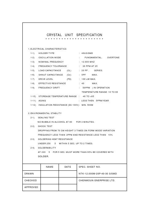
XS12.000M 49USM
Test Machine 1 2 A B
STOREAGE TEMPERATURE RANGE : AGING源自-40 TO +85J
: LESS THEN 5PPM/YEAR
INSULATION RESISTANCE (DC 100V): MIN. 500M[
2. ENVIRONMENTAL STABLITY 2-1) SEALING TEST NO BUBBLE IN ALCOHOL AT 80 J 2-2) SHOCK TEST DROPPING FROM 70 CM HEIGHT 3 TIMES ON FORM WOOD VARIATION FREQUENCY LESS THAN 2PPM AND RESISTANCE LESS THAN 10% 2-3) SOLDERING HEAT RESISTANCE UNDER 250J 2-4) 5J WITHIN 5 SEC. UP TO 2 TIMES. FOR 3 MINUTES.
2-5)
HUMIDITY AT 90-95% RELATIVE HUMIDITY AND 40 ± 2℃ FOR A PERIOD OF MINMUM 8 HOURS SHALL BE LEFT FOR THE PERIOD OF FROM THE HUMIDITY CHAMBER. THE RESULTANT SHALL MEET 1-9 ELECTRICAL CHARATERISTICS.
2-7)
PULL STRENGTH OF TERMINAL APPLY 1KG STATIC LOAD FOR 10 SEC. ALONG THE TERMINAL’S AXIAL DIRECTION.
DIMENSIONS[mm]
HC1 系列多功能,高性能通用變頻調速器 说明书
請勿觸摸內部電路及零部件。
● 運轉時請勿檢查電路板上零部件及信號。 ● 請勿自行拆裝更改變頻器內部連接線或零部件。 ● 變頻器接地端請務必正確接地。 ● 嚴禁私自改裝,更換控制板及零部件,否則有觸電,發生爆炸等危險。
! 注意
● 請勿對變頻器內部的零部件進行耐壓測試,這些半導體零件易受高壓損毀。 ● 絕不可將變頻器輸出端子 U.V.W 連接至交流電源。 ● 變頻器主電路板 CMOS、IC 易受靜電影響及破壞,請勿觸摸主電路板。 ● 只有合格的專業人員才可以安裝、調試及保養變頻器。 ● 變頻器報廢請按工業廢物處理,嚴禁焚燒。
成操作器故障或不顯示。 KM
U
X
●請不要把變頻器安裝在含有爆
變頻器 V W M
炸性氣體的環境裏,否則有引發爆 炸的危險。
X
●在海拔超過 1000 米的地區,變頻 器散熱效果變差,請降檔使用。 ●輸出側請不要安裝接觸器及有關 電容或壓敏電阻,否則會引進變頻 器故障及器件損壞。 輸出側請不要安裝空開和接觸器等 開關器件,如果由於工藝及其他方 面需要必須安裝,則必須保證開關 -3-
變頻器容量,07D5 表示 7.5KW 系列號 商標名稱
-2-
二、安全使用注意事項 二、安全使用注意事項 ⑴送電前
!注意
● 所選用電源電壓必須與變頻器輸入電壓規格相同。
!注意
●
E
端子必須單獨接地,絕對不可接零線,否則極易引起變頻器保護或故障。
● 電源與變頻器之間請不要安裝接觸器,用來操作變頻器的起動或停止,否則,
-5-
三、產品標準規格 ⑵產品通用規格
項目名稱 控制方式 輸入電源 五位元數碼顯示 及狀態指示燈 通信控制 操作溫度 濕度 振動 範圍 精度 頻 率 控 制 設定解析度 輸出解析度 鍵盤設定方式 類比設定方式 其他功能 加減速控制 V/F 曲線 轉矩控制 一 般 控 制 多功能輸入端 多功能輸出端 HC1-A SPWM 380V 電源:330~440V;220V 電源:170~240 顯示頻率、電流、轉速、電壓、計數器、溫度、正反轉狀態、故障 等。 RS-485 -10~40℃ 0~95%相對濕度(不結露) 0.5G 以下 0.10~400.00Hz 數字式:0.01%(-10~40℃) ;模擬式:0.1% (25±10℃) 數字式:0.01Hz;模擬式:最大操作頻率的 1‰ 0.01Hz 可直接以←∧ ∨ 設定 外部電壓 0-5V,0-10V,4—20mA,0—20mA。 頻率下限,啟動頻率,停車頻率、三個跳躍頻率可分別設定 4 段加減速時間(0.1-6500 秒)任意選擇 可任意設定 V/F 曲線 可設定轉矩提升,最大 10.0%啟動轉矩在 1.0Hz 時可達 150% 6 個多功能輸入端,實現 8 段速控制,程式運行,4 段加減速切換, UP、DOWN 機能、計數器,外部急停等功能 有 5 個多功能輸出端,實現運轉中、零速、計數器、外部異常、程 式運行等指示及報警 自動電壓穩壓(AVR) 、減速停止或自由停止、直流刹車,自動重 定再起動,頻率跟蹤,PLC 程式控制、橫動控制、載波可調,最高 達 20KHz 等 電子電驛保護馬達 驅動器(恒轉矩 150%/1 分鐘,風機類 120%/1 分鐘) FUSE 熔斷,馬達停止 220V 線:直流電壓>400V;380V 線:直流電壓>800V 220V 線:直流電壓<200V;380V 線:直流電壓<400V 瞬停後可以頻率跟蹤方式再起動 加/減速運轉中失速防止 電子線路保護 散熱片過熱保護,反轉限制,開機後直接起動及故障複歸之功能, 參數鎖定等。
电调攻略

3.1 电流检测..........................................................................................................................52 3.2 定时器延时与PWM信号 ................................................................................................53
~~~~~~~~~~~~~~~~~~~~~~~~~~~~~~~~~~~~~~~~~~~~~~
By: timegate 墨鸢 技术交流 QQ:1181733110 email:moyuan2000@
第 ii 页
无感无刷直流电机之电调设计全攻略
V0.01
3.4 启动算法..........................................................................................................................63 1. 函数Anwerfen启动流程分析....................................................................................63 2. 启动算法机理探究....................................................................................................65
十速TM57PE12外部中断唤醒应用范例
org 000h
goto main_reset
org 001h
goto interrupt
reti
;-----------------------------------------------------------------------
;-----------------------------------------------------------------------
;%%%%%%%%%%%%%%%%%%%%%%%%%%%% 常数定义 %%%%%%%%%%%%%%%%%%%%%%%%%%%%%%%%%
;-----------------------------------------------------------------------
;XRESETE : External pin Reset Enable(0)
;--------> 1 Enable External pin Reset
;--------> 0 Disable External pin Reset to use as input pin
;!!!!!!!!!!!!!!!!!!!!!!!!!!!!!!!!!!!!!!!!!!!!!!!!!!!!!!!!!!!!!!!!!!!!!!!
;-*-*-*-*-*-*-*-*-*-*-*-*-*-*-*-*-*-*-*-*-*-*-*-*-*-*-*-*-*-*-*--*-*-*-*
;-*-*-*-*-*-*-*-*-*-*-*-*-*-*-*-*-*-*-*-*-*-*-*-*-*-*-*-*-*-*-*--*-*-*-*
施耐德Easy Altivar ATV610 变频器编程手册 说明书
[简单起动] SYS– .......................................................................................32 [Macro-configuration] CFG- 菜单........................................................33 [简单起动] SIM- 菜单...........................................................................34 [修改的参数] LMD- 菜单 .......................................................................38
Easy Altivar ATV610
变频器 编程手册
EAV64393.07 05/2024
法律声明
本文档中提供的信息包含与产品/解决方案相关的一般说明、技术特性和/或建议。
本文档不应替代详细调研、或运营及场所特定的开发或平面示意图。它不用于判定产 品/解决方案对于特定用户应用的适用性或可靠性。任何此类用户都有责任就相关特定 应用场合或使用方面,对产品/解决方案执行或者由所选择的任何业内专家(集成师、 规格指定者等)对产品/解决方案执行适当且全面的风险分析、评估和测试。
对于将本文档 或其内容用作商业用途的行为,施耐德电气未授予任何权利或许可,但 以“原样”为基础进行咨询的非独占个人许可除外。
msp49头文件中文解释
VCC:C=circuit 表示电路的意思, 即接入电路的电压;VDD:D=device 表示器件的意思, 即器件内部的工作电压;VSS:S=series 表示公共连接的意思,通常指电路公共接地端电压。
对于数字电路来说,VCC是电路的供电电压,VDD是芯片的工作电压(通常Vcc>Vdd),VSS 是接地点。
通常在采用正电压的电路上的表示:A VDD--功率(模拟)A VCC—正模拟电源电压A VSS—模拟电路地DVCC—正数字电源电压DVSS—数字电路地A VCC/A VSS一般为模拟部分提供电源,DVCC/DVSS一般为数字部分和内部I/O提供电源,为了避免引入电源干扰,通常需要把AVCC/A VSS和DVCC/DVSS隔离开是这个意思,PxREN的作用是使能上拉或者下拉电阻,因为MSP430F5438这个单片机IO口内部集成了上拉或者下拉电阻,通过PxREN去使能这两个电阻。
另外,IO口有输入和输出两种状态,当IO口是输出状态时,IO口电平高低由单片机控制;当IO口是输入状态时,IO口电平高低由外部电路决定。
IO口输入和输出状态的选择由PxDIR决定,当PxDIR=0时对应IO口的输入状态,PxDIR=1对应IO口的输出状态。
PxOUT的作用是当IO口配置成输出状态时,决定输出电平高低,当IO口配置成输入状态时,并且使能上拉下拉电阻的时候,决定到底是上拉起作用还是下拉电阻起作用。
关于寄存器的配置,你可以看datasheet,或者再有不懂,可以问我。
现在这样理解哈:1.MSP430其实根本没有位操作能力,它为了操作某一位,只能通过操作整个端口来实现;2.位或的时候被0异或的位保持不变,因为有0^0=0;0^1=1; 而与1异或的位取反了,因为0^1=1; 1^1=0;#ifndef __msp430x14x#define __msp430x14x/************************************************************* STANDARD BITS************************************************************/#define BIT0 0x0001#define BIT1 0x0002#define BIT2 0x0004#define BIT3 0x0008#define BIT4 0x0010#define BIT5 0x0020#define BIT6 0x0040#define BIT7 0x0080#define BIT8 0x0100#define BIT9 0x0200#define BITA 0x0400#define BITB 0x0800#define BITC 0x1000#define BITD 0x2000#define BITE 0x4000#define BITF 0x8000/************************************************************ * STATUS REGISTER BITS************************************************************/#define C 0x0001#define Z 0x0002#define N 0x0004#define V 0x0100#define GIE 0x0008#define CPUOFF 0x0010#define OSCOFF 0x0020#define SCG0 0x0040#define SCG1 0x0080/* Low Power Modes coded with Bits 4-7 in SR */#ifndef __IAR_SYSTEMS_ICC /* Begin #defines for assembler */#define LPM0 CPUOFF#define LPM1 SCG0+CPUOFF#define LPM2 SCG1+CPUOFF#define LPM3 SCG1+SCG0+CPUOFF#define LPM4 SCG1+SCG0+OSCOFF+CPUOFF/* End #defines for assembler */#else /* Begin #defines for C */#define LPM0_bits CPUOFF#define LPM1_bits SCG0+CPUOFF#define LPM2_bits SCG1+CPUOFF#define LPM3_bits SCG1+SCG0+CPUOFF#define LPM4_bits SCG1+SCG0+OSCOFF+CPUOFF#include <In430.h>#define LPM0 _BIS_SR(LPM0_bits) /* Enter Low Power Mode 0 */#define LPM0_EXIT _BIC_SR(LPM0_bits) /* Exit Low Power Mode 0 */ #define LPM1 _BIS_SR(LPM1_bits) /* Enter Low Power Mode 1 */#define LPM1_EXIT _BIC_SR(LPM1_bits) /* Exit Low Power Mode 1 */ #define LPM2 _BIS_SR(LPM2_bits) /* Enter Low Power Mode 2 */#define LPM2_EXIT _BIC_SR(LPM2_bits) /* Exit Low Power Mode 2 */ #define LPM3 _BIS_SR(LPM3_bits) /* Enter Low Power Mode 3 */#define LPM3_EXIT _BIC_SR(LPM3_bits) /* Exit Low Power Mode 3 */ #define LPM4 _BIS_SR(LPM4_bits) /* Enter Low Power Mode 4 */#define LPM4_EXIT _BIC_SR(LPM4_bits) /* Exit Low Power Mode 4 */ #endif /* End #defines for C *//************************************************************ * PERIPHERAL FILE MAP************************************************************//************************************************************ * 特殊功能寄存器地址和控制位************************************************************/ /*中断使能1*/#define IE1_ 0x0000sfrb IE1 = IE1_;#define WDTIE 0x01 /*看门狗中断使能*/#define OFIE 0x02 /*外部晶振故障中断使能*/#define NMIIE 0x10 /*非屏蔽中断使能*/#define ACCVIE 0x20 /*可屏蔽中断使能/flash写中断错误*/#define URXIE0 0x40 /*串口0接收中断使能*/#define UTXIE0 0x80 /*串口0发送中断使能*//*中断标志1*/#define IFG1_ 0x0002sfrb IFG1 = IFG1_;#define WDTIFG 0x01 /*看门狗中断标志*/#define OFIFG 0x02 /*外部晶振故障中断标志*/#define NMIIFG 0x10 /*非屏蔽中断标志*/#define URXIFG0 0x40 /*串口0接收中断标志*/#define UTXIFG0 0x80 /*串口0发送中断标志*//* 中断模式使能1 */#define ME1_ 0x0004sfrb ME1 = ME1_;#define URXE0 0x40 /* 串口0接收中断模式使能*/#define USPIE0 0x40 /* 同步中断模式使能*/#define UTXE0 0x80 /* 串口0发送中断模式使能*//* 中断使能2 */#define IE2_ 0x0001sfrb IE2 = IE2_;#define URXIE1 0x10 /* 串口1接收中断使能*/#define UTXIE1 0x20 /* 串口1发送中断使能*//* 中断标志2 */#define IFG2_ 0x0003sfrb IFG2 = IFG2_;#define URXIFG1 0x10 /* 串口1接收中断标志*/#define UTXIFG1 0x20 /* 串口1发送中断标志*//* 中断模式使能2 */#define ME2_ 0x0005sfrb ME2 = ME2_;#define URXE1 0x10 /* 串口1接收中断模式使能*/#define USPIE1 0x10 /* 同步中断模式使能*/#define UTXE1 0x20 /* 串口1发送中断模式使能*//************************************************************* 看门狗定时器的寄存器定义************************************************************/#define WDTCTL_ 0x0120sfrw WDTCTL = WDTCTL_;#define WDTIS0 0x0001 /*选择WDTCNT的四个输出端之一*/#define WDTIS1 0x0002 /*选择WDTCNT的四个输出端之一*/#define WDTSSEL 0x0004 /*选择WDTCNT的时钟源*/#define WDTCNTCL 0x0008 /*清除WDTCNT端: 为1时从0开始计数*/#define WDTTMSEL 0x0010 /*选择模式0: 看门狗模式; 1: 定时器模式*/#define WDTNMI 0x0020 /*选择NMI/RST 引脚功能0:为RST; 1:为NMI*/#define WDTNMIES 0x0040 /*WDTNMI=1时.选择触发延0:为上升延1:为下降延*/#define WDTHOLD 0x0080 /*停止看门狗定时器工作0:启动;1:停止*/#define WDTPW 0x5A00 /* 写密码:高八位*//* SMCLK= 1MHz定时器模式*/#define WDT_MDL Y_32 WDTPW+WDTTMSEL+WDTCNTCL /* TSMCLK*2POWER15=32ms 复位状态*/#define WDT_MDL Y_8 WDTPW+WDTTMSEL+WDTCNTCL+WDTIS0 /* TSMCLK*2POWER13=8.192ms " */#define WDT_MDL Y_0_5 WDTPW+WDTTMSEL+WDTCNTCL+WDTIS1 /* TSMCLK*2POWER9=0.512ms " */#define WDT_MDL Y_0_064 WDTPW+WDTTMSEL+WDTCNTCL+WDTIS1+WDTIS0 /* TSMCLK*2POWER6=0.512ms " *//* ACLK=32.768KHz 定时器模式*/#define WDT_ADL Y_1000 WDTPW+WDTTMSEL+WDTCNTCL+WDTSSEL /* TACLK*2POWER15=1000ms " */#define WDT_ADL Y_250 WDTPW+WDTTMSEL+WDTCNTCL+WDTSSEL+WDTIS0 /* TACLK*2POWER13=250ms " */#define WDT_ADL Y_16 WDTPW+WDTTMSEL+WDTCNTCL+WDTSSEL+WDTIS1 /* TACLK*2POWER9=16ms " */#define WDT_ADL Y_1_9 WDTPW+WDTTMSEL+WDTCNTCL+WDTSSEL+WDTIS1+WDTIS0 /* TACLK*2POWER6=1.9ms " *//* SMCLK=1MHz看门狗模式*/#define WDT_MRST_32 WDTPW+WDTCNTCL /* TSMCLK*2POWER15=32ms 复位状态*/#define WDT_MRST_8 WDTPW+WDTCNTCL+WDTIS0 /* TSMCLK*2POWER13=8.192ms " */#define WDT_MRST_0_5 WDTPW+WDTCNTCL+WDTIS1 /* TSMCLK*2POWER9=0.512ms " */#define WDT_MRST_0_064 WDTPW+WDTCNTCL+WDTIS1+WDTIS0 /* TSMCLK*2POWER6=0.512ms " *//* ACLK=32KHz看门狗模式*/#define WDT_ARST_1000 WDTPW+WDTCNTCL+WDTSSEL /* TACLK*2POWER15=1000ms " */#define WDT_ARST_250 WDTPW+WDTCNTCL+WDTSSEL+WDTIS0 /* TACLK*2POWER13=250ms " */#define WDT_ARST_16 WDTPW+WDTCNTCL+WDTSSEL+WDTIS1 /* TACLK*2POWER9=16ms " */#define WDT_ARST_1_9 WDTPW+WDTCNTCL+WDTSSEL+WDTIS1+WDTIS0 /* TACLK*2POWER6=1.9ms " *//************************************************************硬件乘法器的寄存器定义************************************************************/#define MPY_ 0x0130 /* 无符号乘法*/sfrw MPY = MPY_;#define MPYS_ 0x0132 /* 有符号乘法*/sfrw MPYS = MPYS_;#define MAC_ 0x0134 /* 无符号乘加*/sfrw MAC = MAC_;#define MACS_ 0x0136 /* 有符号乘加*/sfrw MACS = MACS_;#define OP2_ 0x0138 /* 第二乘数*/sfrw OP2 = OP2_;#define RESLO_ 0x013A /* 低6位结果寄存器*/sfrw RESLO = RESLO_;#define RESHI_ 0x013C /* 高6位结果寄存器*/sfrw RESHI = RESHI_;#define SUMEXT_ 0x013E /*结果扩展寄存器*/const sfrw SUMEXT = SUMEXT_;/************************************************************ * DIGITAL I/O Port1/2 寄存器定义有中断功能************************************************************/#define P1IN_ 0x0020 /* P1 输入寄存器*/const sfrb P1IN = P1IN_;#define P1OUT_ 0x0021 /* P1 输出寄存器*/sfrb P1OUT = P1OUT_;#define P1DIR_ 0x0022 /* P1 方向选择寄存器*/sfrb P1DIR = P1DIR_;#define P1IFG_ 0x0023 /* P1 中断标志寄存器*/sfrb P1IFG = P1IFG_;#define P1IES_ 0x0024 /* P1 中断边沿选择寄存器*/sfrb P1IES = P1IES_;#define P1IE_ 0x0025 /* P1 中断使能寄存器*/sfrb P1IE = P1IE_;#define P1SEL_ 0x0026 /* P1 功能选择寄存器*/sfrb P1SEL = P1SEL_;#define P2IN_ 0x0028 /* P2 输入寄存器*/const sfrb P2IN = P2IN_;#define P2OUT_ 0x0029 /* P2 输出寄存器*/sfrb P2OUT = P2OUT_;#define P2DIR_ 0x002A /* P2 方向选择寄存器*/sfrb P2DIR = P2DIR_;#define P2IFG_ 0x002B /* P2 中断标志寄存器*/sfrb P2IFG = P2IFG_;#define P2IES_ 0x002C /* P2 中断边沿选择寄存器*/sfrb P2IES = P2IES_;#define P2IE_ 0x002D /* P2 中断使能寄存器*/sfrb P2IE = P2IE_;#define P2SEL_ 0x002E /* P2 功能选择寄存器*/sfrb P2SEL = P2SEL_;/************************************************************ * DIGITAL I/O Port3/4寄存器定义无中断功能************************************************************/#define P3IN_ 0x0018 /* P3 输入寄存器*/const sfrb P3IN = P3IN_;#define P3OUT_ 0x0019 /* P3 输出寄存器*/sfrb P3OUT = P3OUT_;#define P3DIR_ 0x001A /* P3 方向选择寄存器*/sfrb P3DIR = P3DIR_;#define P3SEL_ 0x001B /* P3 功能选择寄存器*/sfrb P3SEL = P3SEL_;#define P4IN_ 0x001C /* P4 输入寄存器*/const sfrb P4IN = P4IN_;#define P4OUT_ 0x001D /* P4 输出寄存器*/sfrb P4OUT = P4OUT_;#define P4DIR_ 0x001E /* P4 方向选择寄存器*/sfrb P4DIR = P4DIR_;#define P4SEL_ 0x001F /* P4 功能选择寄存器*/sfrb P4SEL = P4SEL_;/************************************************************* DIGITAL I/O Port5/6 I/O口寄存器定义PORT5和6 无中断功能************************************************************/#define P5IN_ 0x0030 /* P5 输入寄存器*/const sfrb P5IN = P5IN_;#define P5OUT_ 0x0031 /* P5 输出寄存器*/sfrb P5OUT = P5OUT_;#define P5DIR_ 0x0032 /* P5 方向选择寄存器*/sfrb P5DIR = P5DIR_;#define P5SEL_ 0x0033 /* P5 功能选择寄存器*/sfrb P5SEL = P5SEL_;#define P6IN_ 0x0034 /* P6 输入寄存器*/const sfrb P6IN = P6IN_;#define P6OUT_ 0x0035 /* P6 输出寄存器*/sfrb P6OUT = P6OUT_;#define P6DIR_ 0x0036 /* P6 方向选择寄存器*/sfrb P6DIR = P6DIR_;#define P6SEL_ 0x0037 /* P6 功能选择寄存器*/sfrb P6SEL = P6SEL_;/************************************************************* USART 串口寄存器"UCTL","UTCTL","URCTL"定义的各个位可串口1 串口2公用************************************************************//* UCTL 串口控制寄存器*/#define PENA 0x80 /*校验允许位*/#define PEV 0x40 /*偶校验为0时为奇校验*/#define SPB 0x20 /*停止位为2 为0时停止位为1*/#define CHAR 0x10 /*数据位为8位为0时数据位为7位*/#define LISTEN 0x08 /*自环模式(发数据同时在把发的数据接收回来)*/#define SYNC 0x04 /*同步模式为0异步模式*/#define MM 0x02 /*为1时地址位多机协议(异步) 主机模式(同步);为0时线路空闲多机协议(异步) 从机模式(同步)*/#define SWRST 0x01 /*控制位*//* UTCTL 串口发送控制寄存器*/#define CKPH 0x80 /*时钟相位控制位(只同步方式用)为1时时钟UCLK延时半个周期*/#define CKPL 0x40 /*时钟极性控制位为1时异步与UCLK相反;同步下降延有效*/#define SSEL1 0x20 /*时钟源选择位:与SSEL0组合为0,1,2,3四种方式*/#define SSEL0 0x10 /*"0"选择外部时钟,"1"选择辅助时钟,"2","3"选择系统子时钟*/#define URXSE 0x08 /*接收触发延控制位(只在异步方式下用)*/#define TXW AKE 0x04 /*多处理器通信传送控制位(只在异步方式下用)*/#define STC 0x02 /*外部引脚STE选择位为0时为4线模式为1时为3线模式*/#define TXEPT 0x01 /*发送器空标志*//* URCTL 串口接收控制寄存器同步模式下只用两位:FE和OE*/#define FE 0x80 /*帧错标志*/#define PE 0x40 /*校验错标志位*/#define OE 0x20 /*溢出标志位*/#define BRK 0x10 /*打断检测位*/#define URXEIE 0x08 /*接收出错中断允许位*/#define URXWIE 0x04 /*接收唤醒中断允许位*/#define RXW AKE 0x02 /*接收唤醒检测位*/#define RXERR 0x01 /*接收错误标志位*//************************************************************* USART 0 串口0寄存器定义************************************************************/#define U0CTL_ 0x0070 /* 串口0基本控制寄存器*/sfrb U0CTL = U0CTL_;#define U0TCTL_ 0x0071 /* 串口0发送控制寄存器*/sfrb U0TCTL = U0TCTL_;#define U0RCTL_ 0x0072 /* 串口0接收控制寄存器*/sfrb U0RCTL = U0RCTL_;#define U0MCTL_ 0x0073 /* 波特率调整寄存器*/sfrb U0MCTL = U0MCTL_;#define U0BR0_ 0x0074 /* 波特率选择寄存器0 */sfrb U0BR0 = U0BR0_;#define U0BR1_ 0x0075 /* 波特率选择寄存器1 */sfrb U0BR1 = U0BR1_;#define U0RXBUF_ 0x0076 /* 接收缓存寄存器*/const sfrb U0RXBUF = U0RXBUF_;#define U0TXBUF_ 0x0077 /* 发送缓存寄存器*/sfrb U0TXBUF = U0TXBUF_;/* 改变的寄存器名定义*/#define UCTL0_ 0x0070 /* UART 0 Control */sfrb UCTL0 = UCTL0_;#define UTCTL0_ 0x0071 /* UART 0 Transmit Control */sfrb UTCTL0 = UTCTL0_;#define URCTL0_ 0x0072 /* UART 0 Receive Control */sfrb URCTL0 = URCTL0_;#define UMCTL0_ 0x0073 /* UART 0 Modulation Control */sfrb UMCTL0 = UMCTL0_;#define UBR00_ 0x0074 /* UART 0 Baud Rate 0 */sfrb UBR00 = UBR00_;#define UBR10_ 0x0075 /* UART 0 Baud Rate 1 */sfrb UBR10 = UBR10_;#define RXBUF0_ 0x0076 /* UART 0 Receive Buffer */const sfrb RXBUF0 = RXBUF0_;#define TXBUF0_ 0x0077 /* UART 0 Transmit Buffer */sfrb TXBUF0 = TXBUF0_;#define UCTL_0_ 0x0070 /* UART 0 Control */sfrb UCTL_0 = UCTL_0_;#define UTCTL_0_ 0x0071 /* UART 0 Transmit Control */sfrb UTCTL_0 = UTCTL_0_;#define URCTL_0_ 0x0072 /* UART 0 Receive Control */sfrb URCTL_0 = URCTL_0_;#define UMCTL_0_ 0x0073 /* UART 0 Modulation Control */sfrb UMCTL_0 = UMCTL_0_;#define UBR0_0_ 0x0074 /* UART 0 Baud Rate 0 */sfrb UBR0_0 = UBR0_0_;#define UBR1_0_ 0x0075 /* UART 0 Baud Rate 1 */sfrb UBR1_0 = UBR1_0_;#define RXBUF_0_ 0x0076 /* UART 0 Receive Buffer */const sfrb RXBUF_0 = RXBUF_0_;#define TXBUF_0_ 0x0077 /* UART 0 Transmit Buffer */sfrb TXBUF_0 = TXBUF_0_;/************************************************************ * USART 1 串口1寄存器定义************************************************************/#define U1CTL_ 0x0078 /* 串口1基本控制寄存器*/sfrb U1CTL = U1CTL_;#define U1TCTL_ 0x0079 /* 串口1发送控制寄存器*/ sfrb U1TCTL = U1TCTL_;#define U1RCTL_ 0x007A /* 串口1接收控制寄存器*/ sfrb U1RCTL = U1RCTL_;#define U1MCTL_ 0x007B /* 波特率调整控制寄存器*/ sfrb U1MCTL = U1MCTL_;#define U1BR0_ 0x007C /* 波特率选择寄存器0 */sfrb U1BR0 = U1BR0_;#define U1BR1_ 0x007D /* 波特率选择寄存器1 */sfrb U1BR1 = U1BR1_;#define U1RXBUF_ 0x007E /* 接收缓存*/const sfrb U1RXBUF = U1RXBUF_;#define U1TXBUF_ 0x007F /* 发送缓存*/sfrb U1TXBUF = U1TXBUF_;/* 改变的寄存器名定义*/#define UCTL1_ 0x0078 /* UART 1 Control */sfrb UCTL1 = UCTL1_;#define UTCTL1_ 0x0079 /* UART 1 Transmit Control */ sfrb UTCTL1 = UTCTL1_;#define URCTL1_ 0x007A /* UART 1 Receive Control */sfrb URCTL1 = URCTL1_;#define UMCTL1_ 0x007B /* UART 1 Modulation Control */ sfrb UMCTL1 = UMCTL1_;#define UBR01_ 0x007C /* UART 1 Baud Rate 0 */sfrb UBR01 = UBR01_;#define UBR11_ 0x007D /* UART 1 Baud Rate 1 */sfrb UBR11 = UBR11_;#define RXBUF1_ 0x007E /* UART 1 Receive Buffer */ const sfrb RXBUF1 = RXBUF1_;#define TXBUF1_ 0x007F /* UART 1 Transmit Buffer */sfrb TXBUF1 = TXBUF1_;#define UCTL_1_ 0x0078 /* UART 1 Control */sfrb UCTL_1 = UCTL_1_;#define UTCTL_1_ 0x0079 /* UART 1 Transmit Control */ sfrb UTCTL_1 = UTCTL_1_;#define URCTL_1_ 0x007A /* UART 1 Receive Control */ sfrb URCTL_1 = URCTL_1_;#define UMCTL_1_ 0x007B /* UART 1 Modulation Control */sfrb UMCTL_1 = UMCTL_1_;#define UBR0_1_ 0x007C /* UART 1 Baud Rate 0 */sfrb UBR0_1 = UBR0_1_;#define UBR1_1_ 0x007D /* UART 1 Baud Rate 1 */sfrb UBR1_1 = UBR1_1_;#define RXBUF_1_ 0x007E /* UART 1 Receive Buffer */const sfrb RXBUF_1 = RXBUF_1_;#define TXBUF_1_ 0x007F /* UART 1 Transmit Buffer */sfrb TXBUF_1 = TXBUF_1_;/************************************************************ * Timer A 定时器A寄存器定义************************************************************/#define TAIV_ 0x012E /* Timer A 中断向量寄存器*/sfrw TAIV = TAIV_;#define TACTL_ 0x0160 /* Timer A 控制寄存器*/sfrw TACTL = TACTL_;#define TACCTL0_ 0x0162 /* Timer A 捕获/比较控制寄存器0 */sfrw TACCTL0 = TACCTL0_;#define TACCTL1_ 0x0164 /* Timer A 捕获/比较控制寄存器1 */sfrw TACCTL1 = TACCTL1_;#define TACCTL2_ 0x0166 /* Timer A 捕获/比较控制寄存器2 */sfrw TACCTL2 = TACCTL2_;#define TAR_ 0x0170 /* Timer A 16位计数器内容*/sfrw TAR = TAR_;#define TACCR0_ 0x0172 /* Timer A 捕获/比较寄存器0 */sfrw TACCR0 = TACCR0_;#define TACCR1_ 0x0174 /* Timer A 捕获/比较寄存器1 */sfrw TACCR1 = TACCR1_;#define TACCR2_ 0x0176 /* Timer A 捕获/比较寄存器2 */sfrw TACCR2 = TACCR2_;/* 改变的寄存器名定义*/#define CCTL0_ 0x0162 /* Timer A Capture/Compare Control 0 */sfrw CCTL0 = CCTL0_;#define CCTL1_ 0x0164 /* Timer A Capture/Compare Control 1 */sfrw CCTL1 = CCTL1_;#define CCTL2_ 0x0166 /* Timer A Capture/Compare Control 2 */sfrw CCTL2 = CCTL2_;#define CCR0_ 0x0172 /* Timer A Capture/Compare 0 */sfrw CCR0 = CCR0_;#define CCR1_ 0x0174 /* Timer A Capture/Compare 1 */sfrw CCR1 = CCR1_;#define CCR2_ 0x0176 /* Timer A Capture/Compare 2 */sfrw CCR2 = CCR2_;/*TACTL 控制寄存器16个位寄存器定义*/#define TASSEL2 0x0400 /* 未用*/#define TASSEL1 0x0200 /* 时钟输入源控制位1 */#define TASSEL0 0x0100 /* 时钟输入源控制位0 */#define ID1 0x0080 /* 分频系数选择位1 */#define ID0 0x0040 /* 分频系数选择位0 */#define MC1 0x0020 /* 计数模式控制位1 */#define MC0 0x0010 /* 计数模式控制位0 */#define TACLR 0x0004 /* 置1位清除定时器*/#define TAIE 0x0002 /* 定时器中断允许*/#define TAIFG 0x0001 /* 定时器中断标志*/#define MC_0 00*0x10 /* 停止模式*/#define MC_1 01*0x10 /* 增计数模式*/#define MC_2 02*0x10 /* 连续计数模式*/#define MC_3 03*0x10 /* 增/减计数模式*/#define ID_0 00*0x40 /* 直通*/#define ID_1 01*0x40 /* 2分频*/#define ID_2 02*0x40 /* 4分频*/#define ID_3 03*0x40 /* 8分频*/#define TASSEL_0 00*0x100 /* 时钟源为TACLK */#define TASSEL_1 01*0x100 /* 时钟源为ACLK */#define TASSEL_2 02*0x100 /* 时钟源为SMCLK */#define TASSEL_3 03*0x100 /* 时钟源为INCLK *//* Timer A ,Timer B 可公用捕获/比较控制寄存器X */#define CM1 0x8000 /* 捕获模式选择位1 */#define CM0 0x4000 /* 捕获模式选择位0 */#define CCIS1 0x2000 /* 捕获输入信号源选择位1 */#define CCIS0 0x1000 /* 捕获输入信号源选择位0 */#define SCS 0x0800 /* 信号同步位0:异步捕获;1:同步捕获*/ #define SCCI 0x0400 /* 锁存输入信号*/#define CAP 0x0100 /* 模式选择: 0:比较模式;1:捕获模式*/ #define OUTMOD2 0x0080 /* 输出模式选择位2 */#define OUTMOD1 0x0040 /* 输出模式选择位1 */#define OUTMOD0 0x0020 /* 输出模式选择位0 */#define CCIE 0x0010 /* 中断允许位*/#define CCI 0x0008 /* 读出输入信号源位ccis0\1 */#define OUT 0x0004 /* 输出信号(选择输出模式0) */#define COV 0x0002 /* 捕获溢出标志*/#define CCIFG 0x0001 /* 中断标志*/#define OUTMOD_0 0*0x20 /* 输出模式*/#define OUTMOD_1 1*0x20 /* 置位模式*/#define OUTMOD_2 2*0x20 /* 翻转/复位模式*/#define OUTMOD_3 3*0x20 /* 置位/复位模式*/#define OUTMOD_4 4*0x20 /* 翻转模式*/#define OUTMOD_5 5*0x20 /* 复位模式*/#define OUTMOD_6 6*0x20 /* 翻转/置位模式*/#define OUTMOD_7 7*0x20 /* 复位/置位模式*/#define CCIS_0 0*0x1000 /* 选择CCIXA为捕获事件的输入信号源*/#define CCIS_1 1*0x1000 /* 选择CCIXB为捕获事件的输入信号源*/#define CCIS_2 2*0x1000 /* 选择GND为捕获事件的输入信号源*/#define CCIS_3 3*0x1000 /* 选择VCC为捕获事件的输入信号源*/#define CM_0 0*0x4000 /* 禁止捕获模式*/#define CM_1 1*0x4000 /* 上升延捕获模式*/#define CM_2 2*0x4000 /* 下降沿捕获模式*/#define CM_3 3*0x4000 /* 上升沿和下降沿都捕获模式*//************************************************************ * Timer B 定时器B寄存器定义************************************************************/#define TBIV_ 0x011E /* 中断向量寄存器:BIT1-BIT3有效*/sfrw TBIV = TBIV_;#define TBCTL_ 0x0180 /* 定时器B控制寄存器:全部控制都集中在这*/ sfrw TBCTL = TBCTL_;#define TBCCTL0_ 0x0182 /* 定时器B捕获/比较控制寄存器0*/sfrw TBCCTL0 = TBCCTL0_;#define TBCCTL1_ 0x0184 /* 定时器B捕获/比较控制寄存器1 */sfrw TBCCTL1 = TBCCTL1_;#define TBCCTL2_ 0x0186 /* 定时器B捕获/比较控制寄存器2 */sfrw TBCCTL2 = TBCCTL2_;#define TBCCTL3_ 0x0188 /* 定时器B捕获/比较控制寄存器3 */sfrw TBCCTL3 = TBCCTL3_;#define TBCCTL4_ 0x018A /* 定时器B捕获/比较控制寄存器4 */sfrw TBCCTL4 = TBCCTL4_;#define TBCCTL5_ 0x018C /* 定时器B捕获/比较控制寄存器5 */sfrw TBCCTL5 = TBCCTL5_;#define TBCCTL6_ 0x018E /* 定时器B捕获/比较控制寄存器6 */sfrw TBCCTL6 = TBCCTL6_;#define TBR_ 0x0190 /* 计数器*/sfrw TBR = TBR_;#define TBCCR0_ 0x0192 /* 定时器B捕获/比较寄存器0 */sfrw TBCCR0 = TBCCR0_;#define TBCCR1_ 0x0194 /* 定时器B捕获/比较寄存器1 */sfrw TBCCR1 = TBCCR1_;#define TBCCR2_ 0x0196 /* 定时器B捕获/比较寄存器2 */sfrw TBCCR2 = TBCCR2_;#define TBCCR3_ 0x0198 /* 定时器B捕获/比较寄存器3 */sfrw TBCCR3 = TBCCR3_;#define TBCCR4_ 0x019A /* 定时器B捕获/比较寄存器4 */sfrw TBCCR4 = TBCCR4_;#define TBCCR5_ 0x019C /* 定时器B捕获/比较寄存器5 */sfrw TBCCR5 = TBCCR5_;#define TBCCR6_ 0x019E /* 定时器B捕获/比较寄存器6 */sfrw TBCCR6 = TBCCR6_;/* 定时器B控制寄存器:全部控制都集中在这*/#define SHR1 0x4000 /* 装载比较锁存器控制位1 :受TBCCTLx中的CCLDx位控制*/#define SHR0 0x2000 /* 装载比较锁存器控制位0 :受TBCCTLx中的CCLDx位控制*/#define TBCLGRP1 0x4000 /* 装载比较锁存器控制位1 :受TBCCTLx中的CCLDx位控制*/ #define TBCLGRP0 0x2000 /* 装载比较锁存器控制位0 :受TBCCTLx中的CCLDx位控制*/ #define CNTL1 0x1000 /* 定时器位数长度控制位1 */#define CNTL0 0x0800 /* 定时器位数长度控制位0 */#define TBSSEL2 0x0400 /* 未用*/#define TBSSEL1 0x0200 /* 时钟输入源控制位1 */#define TBSSEL0 0x0100 /* 时钟输入源控制位0 */#define TBCLR 0x0004 /* 置1清除定时器*/#define TBIE 0x0002 /* 中断允许*/#define TBIFG 0x0001 /* 中断标志*/#define TBSSEL_0 0*0x0100 /* 时钟源为:TBCLK */#define TBSSEL_1 1*0x0100 /* 时钟源为: ACLK */#define TBSSEL_2 2*0x0100 /* 时钟源为:SMCLK */#define TBSSEL_3 3*0x0100 /* 时钟源为:INCLK */#define CNTL_0 0*0x0800 /* 16 位计数模式*/#define CNTL_1 1*0x0800 /* 12 位计数模式*/#define CNTL_2 2*0x0800 /* 10 位计数模式*/#define CNTL_3 3*0x0800 /* 8 位计数模式*/#define SHR_0 0*0x2000 /* 单独装载(初始值) */#define SHR_1 1*0x2000 /* 分三组装载: 1 - 3 groups (1-2, 3-4, 5-6) */#define SHR_2 2*0x2000 /* 分二组装载: 2 - 2 groups (1-3, 4-6)*/#define SHR_3 3*0x2000 /* 不分组装载: 3 - 1 group (all) */#define TBCLGRP_0 0*0x2000 /* 单独装载(初始值) */#define TBCLGRP_1 1*0x2000 /* 分三组装载: 1 - 3 groups (1-2, 3-4, 5-6) */#define TBCLGRP_2 2*0x2000 /* 分二组装载: 2 - 2 groups (1-3, 4-6)*/#define TBCLGRP_3 3*0x2000 /* 不分组装载: 3 - 1 group (all) *//* Additional Timer B Control Register bits are defined in Timer A */#define SLSHR1 0x0400 /* Compare latch load source 1 */#define SLSHR0 0x0200 /* Compare latch load source 0 */#define CLLD1 0x0400 /* 定义比较锁存器TBCLx的装载方式控制位1 */#define CLLD0 0x0200 /* 定义比较锁存器TBCLx的装载方式控制位0 */#define SLSHR_0 0*0x0200 /* 立即装载*/#define SLSHR_1 1*0x0200 /* TBR 计数到0时装载*/#define SLSHR_2 2*0x0200 /* 在增减模式下,计数到TBCLx或0时装载; 在连续计数模式下,计数到0时装载*/#define SLSHR_3 3*0x0200 /* 当计数到TBCL0时装载*/#define CLLD_0 0*0x0200 /* 立即装载*/#define CLLD_1 1*0x0200 /* TBR 计数到0时装载*/#define CLLD_2 2*0x0200 /* 在增减模式下,计数到TBCLx或0时装载; 在连续计数模式下,计数到0时装载*/#define CLLD_3 3*0x0200 /* 当计数到TBCL0时装载*//************************************************************* Basic Clock Module************************************************************/#define DCOCTL_ 0x0056 /* DCO 时钟频率控制寄存器:复位后的值位060h*/sfrb DCOCTL = DCOCTL_;#define BCSCTL1_ 0x0057 /* 系统时钟控制寄存器1 :复位后的值位084h*/sfrb BCSCTL1 = BCSCTL1_;#define BCSCTL2_ 0x0058 /* 系统时钟控制寄存器2 :复位后的值位000h*/sfrb BCSCTL2 = BCSCTL2_;/* DCO 时钟频率控制寄存器*/#define MOD0 0x01 /* DCO插入周期控制位0 */#define MOD1 0x02 /* DCO插入周期控制位1 */#define MOD2 0x04 /* DCO插入周期控制位2 */#define MOD3 0x08 /* DCO插入周期控制位3 */#define MOD4 0x10 /* DCO插入周期控制位4 */#define DCO0 0x20 /* 8种频率控制位0 */#define DCO1 0x40 /* 8种频率控制位1 */#define DCO2 0x80 /* 8种频率控制位2 *//* 系统时钟控制寄存器1 :复位后的值位084h*/#define RSEL0 0x01 /* 选择内部电阻控制位0 */#define RSEL1 0x02 /* 选择内部电阻控制位1 */#define RSEL2 0x04 /* 选择内部电阻控制位2 */#define XT5V 0x08 /* 必须为0*/#define DIVA0 0x10 /* ACLK分频系数控制位0*/#define DIVA1 0x20 /* ACLK分频系数控制位1 */#define XTS 0x40 /* LFXT1工作模式控制位0:低频模式. / 1: 高频模式. */#define XT2OFF 0x80 /* XT2CLK 使能控制位0:开启; 1:关闭*/#define DIVA_0 0x00 /* ACLK分频系数为: 1 */#define DIVA_1 0x10 /* ACLK分频系数为: 2 */#define DIVA_2 0x20 /* ACLK分频系数为: 4 */#define DIVA_3 0x30 /* ACLK分频系数为: 8 *//* 系统时钟控制寄存器2 :复位后的值位000h*/#define DCOR 0x01 /* 内外电阻选择控制位*/#define DIVS0 0x02 /* SMCLK分频控制位0*/#define DIVS1 0x04 /* SMCLK分频控制位1 */#define SELS 0x08 /* SMCLK 时钟源选择位t 0COCLK / 1:XT2CLK/LFXTCLK */ #define DIVM0 0x10 /* MCLK分频控制位0 */#define DIVM1 0x20 /* MCLK分频控制位1 */#define SELM0 0x40 /* MCLK 时钟输入源选择位0 */#define SELM1 0x80 /* MCLK 时钟输入源选择位1 */#define DIVS_0 0x00 /* SMCLK 分频系数为: 1 */#define DIVS_1 0x02 /* SMCLK 分频系数为: 2 */#define DIVS_2 0x04 /* SMCLK 分频系数为: 4 */#define DIVS_3 0x06 /* SMCLK 分频系数为: 8 */#define DIVM_0 0x00 /* MCLK 分频系数为: 1 */#define DIVM_1 0x10 /* MCLK 分频系数为: 2 */#define DIVM_2 0x20 /* MCLK 分频系数为: 4 */#define DIVM_3 0x30 /* MCLK 分频系数为: 8 */#define SELM_0 0x00 /* MCLK 时钟输入源: DCOCLK */#define SELM_1 0x40 /* MCLK 时钟输入源: DCOCLK */#define SELM_2 0x80 /* MCLK 时钟输入源: XT2CLK/LFXTCLK */#define SELM_3 0xC0 /* MCLK 时钟输入源: LFXTCLK *//************************************************************** Flash Memory FLASH操作寄存器定义*************************************************************/#define FCTL1_ 0x0128 /* FLASH控制寄存器1:控制编程、擦除*/sfrw FCTL1 = FCTL1_;#define FCTL2_ 0x012A /* FLASH 控制寄存器2 :控制时钟分频*/sfrw FCTL2 = FCTL2_;#define FCTL3_ 0x012C /* FLASH 控制寄存器3:状态标志*/sfrw FCTL3 = FCTL3_;#define FRKEY 0x9600 /* 读FLASH 密码*/#define FWKEY 0xA500 /* 写FLASH 密码*/#define FXKEY 0x3300 /* for use with XOR instruction */ /* FLASH控制寄存器1:控制编程、擦除*/#define ERASE 0x0002 /* 擦除段使能*/#define MERAS 0x0004 /* 主存擦除使能*/#define WRT 0x0040 /* 编程使能*/#define BLKWRT 0x0080 /* 段编程使能*//* FLASH 控制寄存器2 :控制时钟分频*/#define FN_0 0x0000 /*直通*/#define FN_1 0x0001 /*2分频*/#define FN_2 0x0002 /*3分频*/#define FN_3 0x0003 /*4分频*/#define FN_4 0x0004 /*5分频*/#define FN_5 0x0005 /*6分频*/#define FN_6 0x0006 /*7分频*/#define FN_7 0x0007 /*8分频*/#define FN_8 0x0008 /*9分频*/#define FN_9 0x0009 /*10分频*/#define FN_10 0x000A /*11分频*/#define FN_11 0x000B /*12分频*/#define FN_12 0x000C /*13分频*/#define FN_13 0x000D /*14分频*/#define FN_14 0x000E /*15分频*/#define FN_15 0x000F /*16分频*/#define FN_16 0x0010 /*17分频*/#define FN_17 0x0011 /*18分频*/#define FN_18 0x0012 /*19分频*/#define FN_19 0x0013 /*20分频*/#define FN_20 0x0014 /*21分频*/#define FN_21 0x0015 /*22分频*/#define FN_22 0x0016 /*23分频*/#define FN_23 0x0017 /*24分频*/#define FN_24 0x0018 /*25分频*/#define FN_25 0x0019 /*26分频*/#define FN_26 0x001A /*27分频*/#define FN_27 0x001B /*28分频*/#define FN_28 0x001C /*29分频*/#define FN_29 0x001D /*30分频*/#define FN_30 0x001E /*31分频*/#define FN_31 0x001F /*32分频*/#define FN_32 0x0020 /*33分频*/#define FN_33 0x0021 /*34分频*/#define FN_34 0x0022 /*35分频*/#define FN_35 0x0023 /*36分频*/#define FN_36 0x0024 /*37分频*/#define FN_37 0x0025 /*38分频*/#define FN_38 0x0026 /*39分频*/#define FN_39 0x0027 /*40分频*/#define FN_40 0x0028 /*41分频*/#define FN_41 0x0029 /*42分频*/#define FN_42 0x002A /*43分频*/#define FN_43 0x002B /*44分频*/#define FN_44 0x002C /*45分频*/#define FN_45 0x002D /*46分频*/#define FN_46 0x002E /*47分频*/#define FN_47 0x002F /*48分频*/#define FN_48 0x0030 /*49分频*/#define FN_49 0x0031 /*50分频*/#define FN_50 0x0032 /*51分频*/#define FN_51 0x0033 /*52分频*/#define FN_52 0x0034 /*53分频*/#define FN_53 0x0035 /*54分频*/#define FN_54 0x0036 /*55分频*/#define FN_55 0x0037 /*56分频*/#define FN_56 0x0038 /*57分频*/#define FN_57 0x0039 /*58分频*/#define FN_58 0x003A /*59分频*/#define FN_59 0x003B /*60分频*/#define FN_60 0x003C /*61分频*/#define FN_61 0x003D /*62分频*/#define FN_62 0x003E /*63分频*/#define FN_63 0x003F /*64分频*/#define FSSEL_0 0x0000 /* Flash时钟选择: ACLK */#define FSSEL_1 0x0040 /* Flash时钟选择: MCLK */#define FSSEL_2 0x0080 /* Flash时钟选择: SMCLK */#define FSSEL_3 0x00C0 /* Flash时钟选择: SMCLK *//* FLASH 控制寄存器3:状态标志*/#define BUSY 0x0001 /* Flash忙标志*/#define KEYV 0x0002 /* Flash安全键值出错标志*/#define ACCVIFG 0x0004 /* Flash非法访问中断标志*/#define WAIT 0x0008 /* 等待指示信号位*/#define LOCK 0x0010 /* 锁定位*/#define EMEX 0x0020 /* 紧急退出位*//************************************************************ * Comparator A 比较器A寄存器定义************************************************************/#define CACTL1_ 0x0059 /* 比较器A控制寄存器1 */sfrb CACTL1 = CACTL1_;#define CACTL2_ 0x005A /* 比较器A控制寄存器2 */sfrb CACTL2 = CACTL2_;#define CAPD_ 0x005B /*比较器A端口禁止寄存器*/sfrb CAPD = CAPD_;/* 比较器A控制寄存器1 */#define CAIFG 0x01 /*比较器A中断标志*/#define CAIE 0x02 /* 比较器A中断使能*/#define CAIES 0x04 /* 比较器A中断边沿触发选择0:上升延1:下降延*/ #define CAON 0x08 /* 比较器电源开关*/#define CAREF0 0x10 /* 选择参考源位0 */#define CAREF1 0x20 /* 选择参考源位1 */#define CARSEL 0x40 /* 选择内部参考源加到比较器的正端或负端*/#define CAEX 0x80 /* 交换比较器的输入端*/#define CAREF_0 0x00 /* 选择参考源0 : Off 使用外部参考源*/#define CAREF_1 0x10 /* 选择参考源1 : 0.25*Vcc为参考源*/#define CAREF_2 0x20 /* 选择参考源2 : 0.5*Vcc为参考源*/#define CAREF_3 0x30 /* 选择参考源3 : Vt*//* 比较器A控制寄存器2 */#define CAOUT 0x01 /* 比较器输出*/#define CAF 0x02 /* 选择比较器是否经过RC低通滤波器*/#define P2CA0 0x04 /* 外部引脚信号连接到比较器A的CA0 */#define P2CA1 0x08 /* 外部引脚信号连接到比较器A的CA1 */#define CACTL24 0x10#define CACTL25 0x20#define CACTL26 0x40#define CACTL27 0x80#define CAPD0 0x01 /* Comp. A Disable Input Buffer of Port Register .0 */#define CAPD1 0x02 /* Comp. A Disable Input Buffer of Port Register .1 */#define CAPD2 0x04 /* Comp. A Disable Input Buffer of Port Register .2 */#define CAPD3 0x08 /* Comp. A Disable Input Buffer of Port Register .3 */#define CAPD4 0x10 /* Comp. A Disable Input Buffer of Port Register .4 */#define CAPD5 0x20 /* Comp. A Disable Input Buffer of Port Register .5 */#define CAPD6 0x40 /* Comp. A Disable Input Buffer of Port Register .6 */#define CAPD7 0x80 /* Comp. A Disable Input Buffer of Port Register .7 *//************************************************************* ADC12 A/D采样寄存器定义************************************************************//*ADC12转换控制类寄存器*/#define ADC12CTL0_ 0x0;' /* ADC12 Control 0 */。
镧对稀有鮈鲫肝胰脏抗氧化酶活性及MDA含量的影响

第40卷第2期2019年㊀3月水生态学杂志J o u r n a l o fH y d r o e c o l o g yV o l .40,N o .2M a r .㊀2019D O I :10.15928/j.16743075.2019.02.016㊀㊀收稿日期:20170315基金项目:湖北省教育厅重点项目(D 20131705);福建省特种水产配合饲料重点实验室开放课题(TMK J Z 003).作者简介:华东,1990年生,男,硕士研究生,研究方向为水生生物学.E Gm a i l :1225955454@q q.c o m 通信作者:刘军,1976年生,男,博士,副教授,研究生导师,主要从事水产养殖与水生生物学研究.E Gm a i l :673164434@q q.c o m 镧对稀有鮈鲫肝胰脏抗氧化酶活性及M D A 含量的影响华㊀东1,王剑伟2,胡㊀兵3,刘㊀军1(1.武汉轻工大学动物科学与营养工程学院,湖北武汉㊀430023;2.中国科学院水生生物研究所,湖北武汉㊀430072;3.福建省特种水产配合饲料重点实验室,福建福州㊀350308)摘要:以氯化镧(L a C l 3 7H 2O )为试验毒物,以稀有鮈鲫(G o b i o c y p r i s r a r u s )为试验材料,采用21d 慢性毒性试验(L a 3+浓度分别为0.00㊁0.04㊁0.08㊁0.16㊁0.32㊁0.80m g/L ),通过检测稀有鮈鲫肝胰脏中超氧物歧化酶(S O D )㊁过氧化氢酶(C A T )活性和丙二醛(M D A )含量,研究了镧暴露胁迫对水生动物抗氧化系统的影响,以期从抗氧化生理响应的角度探讨稀土元素镧对水生动物的毒理机理.结果显示,与对照组相比,0 04~0 32m g /L 试验组肝胰脏S O D 活性出现一定程度降低(P >0.05),但0.80m g/L 组S O D 活性出现一定程度上升(P >0.05);0 04~0.32m g /L 试验组肝胰脏C A T 活性较对照组出现一定程度降低(P >0.05),但0.80m g /L 组C A T 活性出现一定程度上升(P >0.05),且0.80m g /L 组C A T 活性显著高于0.04~0.32m g /L 组(P <0.05);0.04~0.16m g /L 试验组肝胰脏M D A 含量较对照组出现一定程度降低(P >0.05),0.32m g/L 组M D A 含量略微升高(P >0.05),0.80m g/L 组M D A 含量显著高于对照组(P <0.05),也显著高于其它L a 3+暴露组(P <0.05).研究表明,一定浓度的L a3+暴露胁迫会对环境中水生生物抗氧化系统产生不利影响.关键词:稀有鮈鲫;镧;超氧化物歧化酶;过氧化氢酶;丙二醛中图分类号:Q 355㊀㊀文献标志码:A㊀㊀文章编号:16743075(2019)02010806㊀㊀我国稀土资源丰富,在其开发和冶炼过程中,由于监管不到位㊁非法开采㊁工艺落后㊁ 三废 排放等原因,导致矿区周边水体和土壤稀土元素㊁重金属和浸矿剂污染比较严重.稀土尾矿在降雨的冲刷和淋滤下,稀土元素㊁重金属等污染物质排入水体和土壤,导致农田绝收㊁水体生物多样性下降,周边居民的身体健康受到严重危胁(高志强和周启星,2011).研究表明,通过植物吸收和富集,稀土经过食物链进入动物和人体内并因此产生毒害作用(Y a n g et a l ,2009).赣南矿区成人日摄入稀土量为6.0~6.7m g ,比对照区成人摄入量高2倍(温小军,2012).在稀土矿区采集成人血液进行研究,发现稀土暴露地区人群的外周血单核细胞的端粒酶活性提高,外周血单核细胞S 期和G 2GM 期增加,稀土元素还影响D N A 的复制(Y u e t a l ,2007).长期摄入低剂量的稀土,将导致儿童智商发育不良,成人中枢神经传导显著下降,儿童肺活量和血压较低,免疫蛋白I gM 水平显著降低(夏青等,2012).目前,有关稀土对水生动物及水域生态系统影响的研究较少,对鱼类抗氧化系统研究鲜有报道,且均未采用标准推荐实验动物(张贵生,2007).超氧化物歧化酶(S O D )㊁过氧化氢酶(C A T )㊁丙二醛(M D A )在脊椎动物体内抗氧化系统中有重要作用.因此,许多学者通过检测上述指标来研究污染物胁迫对生物抗氧化系统产生的影响(B i c z a ke ta l ,2017).本研究以氯化镧(L a C l 3 7H 2O )为试验毒物,以推荐标准试验动物稀有鮈鲫(G o b i o c y p r i s r a Gr u s )为试验材料,通过慢性毒性试验,以S O D ㊁C A T ㊁MD A 为指标,研究氯化镧暴露对水生动物抗氧化系统的影响,以期评价稀土长期暴露对鱼类慢性毒性效应,旨在为监测稀土污染㊁评价其对水域生态环境潜在胁迫及制定环境保护措施提供参考.1㊀材料和方法1.1㊀试验鱼试验鱼为实验室饲养的稀有鮈鲫,由中国科学院水生生物研究所提供,体长(3.34ʃ0.35)c m ,体重(0.56ʃ0.11)g .从养殖群体中选择游泳速度正常㊁体表无损伤的个体,试验鱼在60c mˑ40c mˑ40c m的水族箱内暂养7d,溶氧大于5m g/L.每日定时投喂冷冻赤虫2次,暂养期间活动正常,死亡率在5%以下,每天定时换水和清除残渣.正式试验前1d停止投喂,随机分组进行试验.1.2㊀试验用水和试剂试验用水为曝气2d的去离子水.氯化镧(L a C l3 7H2O,分析纯,99.99%,美国S i g m a公司).镧一级储备液,L a3+浓度为1000m g/L;二级储备液,L a3+浓度为100m g/L.蛋白定量测试盒㊁S O D㊁C A T㊁M D A试剂盒均购于南京建成生物工程研究所.1.3㊀仪器和设备试验的仪器和设备包括i M a r k酶标仪㊁DWG86L486型超低温保存箱㊁S o r v a l l S t r a t o s冷冻高速离心机㊁D K BG501A型超级恒温水槽㊁B C DG189U/B 型低温冰箱㊁玻璃匀浆器㊁WHG2微型漩涡混合仪㊁E p p e n d o r f移液枪㊁电子天平等.1.4㊀试验方法试验容器均为矩形玻璃缸,长ˑ宽ˑ高尺寸为30c mˑ20c mˑ20c m,最大容积为10L.试验期间水温(22.48ʃ1.07)ħ;溶氧(5.63ʃ1.09)m g/L; p H值(6.17ʃ0.19);光暗比12/12.根据急性毒性试验数据(96h L C50=1.92m g/L),本试验设计5个浓度组,即0.04㊁0.08㊁0.16㊁0.32㊁0.80m g/L和1个空白对照组,每组均设3个平行,每个平行组8条鱼.每天定时投喂2次赤虫,及时清理鱼缸,每2d换水1.5L.在暴露21d后采样,每缸随机挑选2尾鱼,吸干鱼体表水分,然后在解剖盘中分离出肝胰脏组织,将组织用滤纸拭干后,在1/105电子称称量,然后装入自封袋中做好标记,立即置于80ħ冰箱保存.准确称取组织样品约0.2g,用眼科剪刀快速剪碎组织后置于玻璃匀浆器中,按1ʒ9(W/V)加入0.9%的预冷生理盐水,在冰水浴中匀浆,研磨5~10m i n,然后将匀浆液转移至5m L离心管中,在4ħ下3000r/m i n 离心10m i n,取上清液.按照试剂盒的具体操作测定酶活性以及M D A含量.1.5㊀数据分析试验所得数据用S P S S17.0统计软件处理,采用单因素方差分析(O n eGw a y A N O V A),运用多重比较(L S D)进行差异显著性检验.试验数据表示为平均值ʃ标准差(MʃS D),P<0.05表示与对照组具有显著差异.2㊀结果2.1㊀镧对稀有鮈鲫肝胰脏S O D活性的影响镧对稀有鮈鲫肝胰脏S O D活性的影响见表1和图1.方差分析表明,各处理组间差异不显著(P >0.05).对照组S O D活性为(79 50ʃ19.01)U/m g.与对照组相比,0.04~0.32m g/L试验组肝胰脏S O D活性出现一定程度降低(P>0.05),但0.80m g/L组S O D活性出现一定程度上升(P>0.05).表1㊀镧对肝胰脏S O D、C A T活性及M D A含量影响T a b.1㊀E f f e c t o f l a n t h a n u mo nS O Da n dC A Ta c t i v i t y a n d M D Ac o n t e n t i n t h e h e p a t o p a n c r e a s o f G.r a r u s试验浓度/m g L1S O D活性/U m g1C A T活性/U m g1M D A含量/n m o l m g10.0079.50ʃ19.0151.25ʃ6.07a b2.51ʃ1.02a 0.0469.72ʃ17.0945.84ʃ4.37a2.30ʃ0.18a 0.0866.42ʃ8.5244.15ʃ11.25a2.42ʃ0.66a 0.1669.60ʃ10.7440.22ʃ10.00a2.24ʃ0.45a 0.3269.79ʃ11.1342.22ʃ14.33a2.52ʃ0.40a 0.8084.50ʃ6.3158.18ʃ8.19b6.07ʃ1.41b ㊀㊀注:同列上标不同字母表示差异显著(P<0.05).N o t e:D i f f e r e n t l e t t e r s i nt h es a m ec o l u m ni n d i c a t es i g n i f i c a n t d i f f e r e n c e a t t h e l e v e l o f0.05.图1㊀镧对稀有鮈鲫肝胰脏S O D活性的影响F i g.1㊀E f f e c t o f l a n t h a n u mo nh e p a t o p a n c r e a t i c S O Da c t i v i t y 2.2㊀镧对稀有鮈鲫肝胰脏C A T活性的影响镧对稀有鮈鲫肝胰脏C A T活性的影响见表1和图2.方差分析表明,各处理组间存在显著差异(P<0.05).C A T活性变化趋势同S O D一致.对照组C A T活性为(51.25ʃ6.07)U/m g.0 04~0 32m g/L试验组肝胰脏C A T活性较对照组相比出现一定程度降低(P>0.05),但0.80m g/L组C A T活性有一定程度上升(P>0.05),且0.80m g/L组C A T活性显著高于0.04~0.32m g/L 组(P<0.05).9012019第2期㊀㊀㊀㊀㊀㊀㊀㊀华㊀东等,镧对稀有鮈鲫肝胰脏抗氧化酶活性及M D A含量的影响图2㊀镧对稀有鮈鲫肝胰脏C A T 活性的影响F i g .2㊀E f f e c t o f l a n t h a n u mo nh e p a t o pa n c r e a t i c C A Ta c t i v i t y2.3㊀镧对稀有鮈鲫肝胰脏M D A 含量的影响镧对稀有鮈鲫肝胰脏M D A 含量的影响见表1和图3.方差分析表明,各处理组间存在显著差异(P <0.05).对照组M D A 含量为(2 51ʃ1.02)n m o l /m g .与对照组相比,0.04~0.16m g /L 试验组肝胰脏M D A 含量出现一定程度降低(P >0.05),但0 32m g /L 组肝胰脏M D A 含量略有升高(P >0.05).0.80m g/L 组肝胰脏M D A 含量显著高于对照组(P <0.05),也显著高于其它L a 3+暴露组(P <0.05).图3㊀镧对稀有鮈鲫肝胰脏M D A 含量的影响F i g.3㊀E f f e c t o f l a n t h a n u mo n M D Ac o n t e n t o f t h e h e p a t o pa n c r e a s 3㊀讨论机体中的抗氧化酶系统在维持氧自由基代谢平衡方面起着十分重要的作用(P a l a c e ae t a l ,1998).在代谢过程中,机体可生成活性氧中间体,如O H G㊁O G2和H 2O 2等,这些自由基若不及时消除,就会对机体造成氧化胁迫,引起酶失活㊁脂质过氧化,进而有可能导致D N A 断裂㊁癌症㊁机体死亡等.氧自由基是一类具有高度化学反应活性的基团,对机体产生毒性作用,甚至导致睾丸生精功能障碍(R e e se ta l ,2008).正常的生理情况下,存在一些细胞抗氧化防御机制来调节活性氧的生产,包括酶和非酶的途径,以保护生物系统免受自由基的毒性(P e t e r e ta l ,2016).超氧化物歧化酶(S O D )㊁过氧化氢酶(C A T )㊁丙二醛(M D A )在脊椎动物体抗氧化系统中扮演重要角色(T o d o r o v a e t a l ,2005).当动物暴露于污染物时,这些污染物参与了体内氧化还原循环并产生大量的活性氧物质,S O D ㊁C A T 活性及M D A含量随之改变.因此,许多学者通过检测上述指标来研究污染物胁迫对生物造成的毒性效应.3.1㊀不同胁迫程度与S O D 活性的变化S O D 能以超氧阴离子自由基(O G2)为底物进行反应,是生物体内一种重要金属酶类(焦传珍,2009).当生物体受到环境的轻度威胁时,S O D 活性会被诱导升高,在受到重度威胁时,则会出现抑制S O D 活性的情况(邰托娅等,2008);随着胁迫时间及浓度的增加,S O D 活性在铵态氮浓度3.82m g /L 时出现升高现象(A n n a e t a l ,2014);当胁迫程度不断加强时,抗氧化系统不能及时清除超过一定阈值或长期去除自由基,自由基对细胞产生氧化损伤(A n aM a r ía e t a l ,2014);抗氧化系统被破坏,抗氧化酶活性降低(B a r b a r a&A n d r z e j ,2016).金芬芬等(2011)研究发现,低浓度镉离子会诱导长江华溪蟹肝胰腺线粒体S O D 活性增强,高浓度镉离子中过多的镉离子会使S O D 活性降低;张贵生(2007)认为L a 3+浓度较低时(0.1m g/L ),鲤大脑中S O D 的活性增强,而肌肉㊁肝胰脏㊁肾脏㊁鱼鳃中的S O D 活性均会降低,在较高浓度(2m g /L 和5m g /L )的试验组中,这5种组织中的S O D 活性均降低.本实验中,低浓度组肝胰脏S O D 活性低于空白对照组,而高浓度组(0.80m g/L )S O D 活性高于对照组,表明随着稀土L a3+浓度的上升,稀有鮈鲫肝胰脏S O D 活性受到的影响是不同的,这与上述文献报道存在差异.其原因可能是:(1)采用的试验动物不同,染毒物质不同,不同动物对同一毒物的敏感性可能不同,同一毒物对不同动物的作用机制也可能不同;(2)检测的S O D 活性组织来源不同,敏感性存在差异(S a m a r gh a n d i a ne t a l ,2017);(3)不同试验设置的染毒物浓度存在差别,其毒性存在剂量效应(M e a d o r ,2015);(4)不同试验的染毒时间存在差异,其毒性存在时间效应(P l e t z e t a l ,2016).3.2㊀不同胁迫程度与C A T 活性的变化C A T 是生物体内一种抗氧化防御酶,可以清除S OD 反应后产生的H 2O 2,其活性高,会加快分解H 2O 2,产生H 2O 和O 2的速率.当毒物在一定范围内增加时,会诱导C A T 活性增强,但当污染物浓011第40卷第2期㊀㊀㊀㊀㊀㊀㊀㊀㊀㊀水生态学杂志㊀㊀㊀㊀㊀㊀㊀㊀㊀㊀㊀㊀㊀㊀㊀㊀㊀㊀2019年3月度增加到一定程度后,C A T活性会下降.薛细平等(2003)建立了简便的过氧化氢酶测定方法,通过监测过氧化氢酶活性,能反映出污染本质及其早期影响,同时在保护环境资源方面有一定的预报作用.本研究中,L a3+低浓度组(0.04~0.32m g/L)肝胰脏C A T活性较对照组相比出现一定程度降低,0.80m g/L组C A T活性出现一定程度上升,这与前面S O D活性变化一致;张清顺等(2009)的研究中也出现类似现象.当暴露浓度到达0.80m g/L组时, C A T活性增加,其原因可能是较少的L a3+进入机体并诱导其产生活性氧自由基时,S O D活性被诱导,进而促使机体内H2O2含量升高;而H2O2的升高会诱导机体内C A T的基因表达及活力,以提高H2O2的分解速率(C h e ne t a l,1994);但也有研究认为,随着污染物浓度的进一步增大,最终会产生大量不能尽快清除的OG2,会反过来降低C A T活性(王凡等,2010).3.3㊀不同胁迫程度与M D A含量的变化M D A是生物体内脂质过氧化反应的主要产物.当发生脂质过氧化时,产生的自由基会攻击细胞膜,最终产生致突变㊁致癌的M D A(M a r i a ne t a l,2016).随着毒物浓度的增加,脂质过氧化损伤加剧,M D A含量升高.程媛媛等(2015)以萼花臂尾轮虫为试验动物研究氨氮的毒性机制,发现M D A 含量变化灵敏,可用M D A作为指标来检测氨氮对其的急性毒性效应;金芬芬等(2011)研究发现,增大镉离子浓度会诱导长江华溪蟹肝胰腺线粒体M D A 含量显著升高;张贵生(2012)研究发现,增大L a3+浓度会促使鲤血液中丙二醛含量升高,且高浓度组与对照组差异显著.本实验中,较低浓度组(0.04~0.16m g/L) M D A含量低于对照组(P>0.05),而较高浓度(0.32m g/L和0.80m g/L)M D A含量增加或显著增加(P<0.05),与上述文献报道结论基本一致.高浓度L a3+暴露组M D A含量增加,究其原因:一方面L a3+诱导机体产生大量的活性氧自由基,从而导致脂质过氧化的发生(Z a b a l z ae t a l,2007);另一方面,L a3+抑制了抗氧化酶活力,减少了抗氧化剂G S H的含量,降低了线粒体清除活性氧自由基的能力,从而导致其发生严重的氧化损伤(O t e i z ae t a l,1997).3.4㊀稀土对水生动物及水域生态的影响我国稀土资源丰富,在其开发和冶炼过程中,由于监管不到位以及 三废 排放等原因,导致矿区周边水体和土壤稀土元素污染比较严重(朱建华等,2002);此外,稀土元素作为一种饲料添加剂已在我国水产养殖中广泛应用,由于残饵㊁粪便的原因,必将导致水体中稀土元素含量的增加.稀土进入生态环境,不可避免地间接或直接对生物产生影响,甚至通过食物链进入人体.本研究中,0.80m g/LL a3+暴露组,稀有鮈鲫肝胰脏中C A T活性显著上升,M D A含量显著升高,表明一定浓度的L a3+暴露胁迫,可诱导水生动物肝脏发生氧化应激反应.由于稀土具备独特的生物学和毒理学效应.因此,在大力开发和利用稀土元素的同时,其可能产生的水域生态环境问题及对人体健康的影响应该引起足够的重视.参考文献程媛媛,顾若波,王小林,等,2015.氨氮对萼花臂尾轮虫的急性毒性及其抗氧化生理响应[J].安徽农业科学,43(36):8184,363.高志强,周启星,2011.稀土矿露天开采过程的污染及对资源和生态环境的影响[J].生态学杂志,30(12):29152922.焦传珍,2009.铈对镉染毒泥鳅肝胰脏中超氧化物歧化酶和过氧化物酶活性的影响[J].水产科学,28(12):786788.金芬芬,徐团,秦圣娟,等,2011.镉对长江华溪蟹肝胰腺线粒体抗氧化酶活力和脂质过氧化水平的影响[J].水生生物学报,35(6):10201024.吕玥,张迎梅,杨峰,等,2010.壬基酚对中华大蟾蜍蝌蚪的毒性效应[J].农业环境科学学报,29(6):10861090.苗菲菲,司万童,刘菊梅,等,2012.尾矿库渗漏水导致泥鳅氧化损伤与D N A损伤的研究[J].广东农业科学, (16):162164.邰托娅,林玉锁,贺静,2008.土壤中C u和P b单一及复合污染对蚯蚓体内蛋白含量和S O D活性的影响[J].农业环境科学学报,27(5):19851990.王凡,刘海芳,晋冬梅,等,2010.镉污染对鲤鱼过氧化氢酶活性的影响[J].水产科学,29(9):550552.王立军,梁涛,章申,等,2004.外施稀土在农田生态系统中的生物地球化学循环与残留[J].中国稀土学报,22(5):676681.温小军,2012.赣南稀土矿区土壤环境特征及稀土金属地球化学行为研究[D].昆明:云南大学.夏青,刘会雪,杨晓达,等,2012.稀土神经毒性研究[J].中国科学(化学),42(9):13081314.薛细平,陈荣,赵一兵,等,2003.过氧化氢酶的荧光法测定及其在海洋环境污染评估中的应用[J].厦门大学学报(自然科学版),42(1):8386.1112019第2期㊀㊀㊀㊀㊀㊀㊀㊀华㊀东等,镧对稀有鮈鲫肝胰脏抗氧化酶活性及M D A含量的影响张贵生.2007.氯化镧对鲤鱼多种酶㊁过氧化脂质及遗传毒性的影响研究[D].济南:山东师范大学.张清顺,侯建军,刘香江,等,2009.铜对梨形环棱螺抗氧化酶活性和金属硫蛋白含量的影响[J].水生生物学报,33(4):717725.朱建华,袁兆康,王晓燕,等,2002.江西稀土矿区环境稀土含量调查[J].环境与健康杂志,19(6):443444.A n aM a ríaM e n d o z aGW i l s o n,S e r g i o I v a nC a s t r oGA r r e d o n d o, R e néR e n a t oB a l a n d ránGQ u i n t a n a,2014.C o m p u t a t i o n a l s t u d y o f t h es t r u c t u r eGf r e er a d i c a l s c a v e n g i n g r e l a t i o nGs h i p o f p r o c y a n i d i n s[J].O r i g i n a l R e s e a r c h A r t i c l e,161:155161.A n n aE,H e i n k A m b e rN,P a r r i s hG s a r y H T h o r g a a r d,e t a l,2014.O x i d a t i v es t r e s sa m o n g S O DG1g e n o t y p e si n r a i n b o w t r o u t(O n c o r h y n c h u s m y k i s s)[J].A q u a t i c T o x i c o l o g y,156:19.A n w e rT,S h a r m a M,P i l l a iK K,e ta l,2007.P r o t e c t i v e e f f e c t o fb e z a f i b r a t eo ns t r e p t o z o t o c i nGi n d u c e do x i d a t i v e s t r e s sa n dt o x i c i t y i nr a t s[J].T o x i c o l o g y,229(1/2):165172.B a r b a r a N i e r a d k oGI w a n i c k a,A n d r z e j B o r z e c k i,2016.T h e 28Gd a y e x p o s u r et of e n p r o p a t h r i nd e c r e a s e sl o c o m o t o r a c t i v i t y a n dr e d u c e sa c t i v i t y o fa n t i o x i d a n te n z y m e si n m i c eb r a i n s[J].P h a r m a c o l o g i c a lR e p o r t s,68(2):495501.B i c z a kR,S n i o s z e k M,T e l e s ińs k iA,e ta l,2017.G r o w t h i n h i b i t i o na n de f f i c i e n c y o ft h ea n t i o x i d a n ts y s t e m i n s p r i n g b a r l e y a n d c o mm o n r a d i s h g r o w n o n s o i l p o l l u t e d i o n i c l i q u i d sw i t hi o d i d ea n i o n s[J].E c o t o x i c o lE n v i r o n S a f,139:463471.C h e nT,F u r s tA,C h i e nPK,1994.T h e e f f e c t s o f c a d m i u m a n d i r o n o n c a t a l a s e a c t i v i t i e s i nT u b i f e k[J].T h eA m e rGi c a nC o l l e g e o fT o x i c o l o g y,13(2):112113.M a r i a nV a l k o,K l a u d i aJ o m o v a,C h r i s t o p h e rJR h o d e s,e t a l,2016.R e d o xGa n dn o nGr e d o xGm e t a lGi n d u c e d f o r m a t i o n o f f r e e r a d i c a l s a n d t h e i r r o l e i nh u m a nd i s e a s e[J].A rGc h i v e s o fT o x i c o l o g y,90(1):137.M e a d o r JP,2015.T i s s u ec o n c e n t r a t i o n sa s t h ed o s e m e t r i c t oa s s e s s p o t e n t i a l t o x i c e f f e c t s o fm e t a l s i n f i e l dGc o l l e c tGe df i s h:C o p p e ra n d C a d m i u m[J].E n v i r o n T o x i c o l C h e m,34(6):13091319.O t e i z aP I,U c h i t e lOD,C a r r a s q u e d oF,e t a l,1997.E v a l uGa t i o no f a n t i o x i d a n t s,p r o t e i n,a n d l i p i do x i d a t i o n p r o dGu c t s i nb l o o d f r o ms p o r a d i c a m y o t r o p h i c l a t e r a l s c l e r o s i s p a t i e n t s[J].N e u r oGc h e m i c a lR e s e a r c h,22(4):535539.P a l a c e aVP,B r o w nSB,B a r o nC I,e t a l,1998.A n e v a l u aGt i o no f t h e r e l a t i o n s h i p s a m o n g o x i d a t i v e S t r e s s,a n t i o xGi d a n t v i t a m i n s a n de a r l y m o r t a l i t y s y n d r o m e(E M S)o f L a k eT r o u t(S a l v e l i n u s n a m e y c u s h)f r o mL a k eO n t a r i o [J].A q u a t i cT o x i c o l o g y,43(23):259268.P e t e rP a t l e v i c a,J a n k a V ašk o v b,P a v o lS v o r cJ r c,e ta l,2016.R e a c t i v e o x y g e n s p e c i e s a n d a n t i o x i d a n t d e f e n s e i n h u m a n g a s t r o i n t e s t i n a l d i s e a s e s[J].I n t e g r a t i v eM e d i c i n e R e s e a r c h,5(4):250258.P l e t z,J u l i a,Sán c h e zGB a y o,F r a n c i s c o,T e n n e k e s,H e n kA,2016.D o s eGr e s p o n s ea n a l y s i s i n d i c a t i n g t i m eGd e p e n d e n t n e u r oGt o x i c i t y c a u s e db y o r g a n i c a n d i n o r g a n i cm e r c u r yGI m p l i c a t i o n s f o r t o x i c e f f e c t s i n t h e d e v e l o p i n g b r a i n[J].T o x i c o l o g y,347/349:15.R e e sM D,K e n n e t tEC,W h i t e l o c kJM,e t a l,2008.O x iGd a t i v e d a m a g e t o e x t r a c e l l u l a rm a t r i x a n d i t s r o l e i nh uGm a n p a t h o l o g i e s[J].F r e e R a d i c B i o l M e d,44(12):19732001.S a m a r g h a n d i a nS,A z i m iGN e z h a d M,F a r k h o n d e hT,e t a l,2017.A n t iGo x i d a t i v e e f f e c t s o f c u r c u m i no n i mm o b i l i z aGt i o nGi n d u c e do x i d a t i v e s t r e s s i n r a t b r a i n,l i v e r a n dk i dGn e y[J].B i o m e dP h a r m a c o t h e r,87:223229.T o d o r o v a I,S i m e o n o v aG,K y u c h u k o v aD,e t a l,2005.R e fGe r e n c ev a l u e s o f o x i d a t i v e s t r e s s p a r a m e t e r s(M D A, S O D,C A T)i nd o g sa n dc a t s[J].C o m p a r a t i v eC l i n i c a l P a t h o l o g y,13(4):190194.Y a n g J,L i uQ,Z h a n g L,e t a l,2009.L a n t h a n u mc h l o r i d e i m p a i r s m e m o r y,d e c r e a s e s p C a MKI V,p MA P K a n d p C R E Be x p r e s s i o n o f h i p p o c a m p u s i n r a t s[J].T o x i c o l oGg y L e t t e r s,190(2):208214.Y uL,D a i YC,Y u a nZK,e t a l,2007.E f f e c t s o f r a r e e a r t h e l e m e n t s o n t e l o m e r a s e a c t i v i t y a n da p o p t o s i so f h u m a n p e r i p h e r a l b l o o dm o n o n u c l e a r c e l l s[J].B i o l o g i c a lT r a c e E l e m e n tR e s e a r c h,116(1):5359.Z a b a l z aA,G a s t o nS,M a r i aS,e t a l,2007.O x i d a t i v e s t r e s s i sn o t r e l a t e d t o t h em o d e o f a c t i o n o f h e r b i c i d e s t h a t i nGh i b i t a c e t o l a c t a t es y n t h a s e[J].E n v i r o n m e n t a la n d E xGp e r i m e n t a l B o t a n y,59(2):150159.(责任编辑㊀万月华)211第40卷第2期㊀㊀㊀㊀㊀㊀㊀㊀㊀㊀水生态学杂志㊀㊀㊀㊀㊀㊀㊀㊀㊀㊀㊀㊀㊀㊀㊀㊀㊀㊀2019年3月E f f e c t o fL a n t h a n u mE x p o s u r e o n t h eA n t i o x i d a s eA c t i v i t y an dM D AC o n t e n t i n t h eH e p a t o pa n c r e a s o f G ob i oc y p r i s r a r u s HU A D o n g 1,WA N GJ i a n Gw e i 2,HU B i n g 3,L I UJ u n 1(1.S c h o o l o fA n i m a l S c i e n c e a n dN u t r i t i o n a l E n g i n e e r i n g ,W u h a nP o l yt e c h n i c U n i v e r s i t y,W u h a n ㊀430023,P .R.C h i n a ;2.I n s t i t u t e o fH y d r o b i o l o g y ,C h i n e s eA c a d e m y of S c i e n c e s ,W u h a n ㊀430072,P .R.C h i n a ;3.F u j i a nK e y L a b o r a t o r y o f S p e c i a lA qu a t i cF o r m u l aF e e d ,F u z h o u ㊀350308,P .R.C h i n a )A b s t r a c t :T h e p r e s e n c e o f r a r e e a r t h e l e m e n t s (R E E )i n s u r f a c e r u n o f f a n dw a s t e w a t e r a s s o c i a t e dw i t h t h ee x c a v a t i o na n d s m e l t i n g o fR E Et h r e a t e n s a q u a t i c e c o s y s t e m s .R e s e a r c ho nt h eef f e c t so fR E Eo na qu a t i c o r g a n i s m s i s l a c k i n g ,p a r t i c u l a r l y r e g a r d i n g t h e t o x i c e f f e c t s a n d t o x i c o l o g i c a lm e c h a n i s m s .T h e r a r em i n Gn o w (G o b i o c y pr i s r a r u s )i s r e c o mm e n d e d a s a t e s t o r g a n i s m ,a c c o r d i n g t o t h e g u i d e l i n e s f o r t h e t e s t i n g o f c h e m i c a l s (M i n i s t r y o fE n v i r o n m e n t a lP r o t e c t i o no fC h i n a ).T oe x p l o r et h et o x i c o l o gi c a lm e c h a n i s m o f R E E i na q u a t i c a n i m a l s ,w e p e r f o r m e dac h r o n i c t o x i c i t y t e s t t oe x a m i n e t h ea n t i o x i d a n t r e s po n s eo f t h e r a r em i n n o wt od i f f e r e n t c o n c e n t r a t i o n s o f l a n t h a n u m (L a 3+).T h e f i s hw e r e r e a r e d i n f r e s h w a t e r a n de x Gp o s e d t o 0.00,0.04,0.08,0.16,0.32a n d 0.80m g /LL a 3+f o r 21d .T h e a c t i v i t i e s o f s u pe r o x i d e d i s m u t a s e (S O D )a n d c a t a l a s e (C A T )a n d t h e c o n t e n t o fm a l o n d i a l d e h y d e (M D A )i n t h e h e p a t o pa n c r e a s o f t e s tm i n Gn o w sw e r e a n a l y z e d .I n t h e c o n t r o l g r o u p ,S O Da c t i v i t y i n t h e h e p a t o p a n c r e a sw a s (79.50ʃ19.01)U /m g.S O Da c t i v i t i e sa t t h el o w e rL a 3+e x p o s u r e s (0.040.32m g /L )w e r el o w e rt h a ni nt h ec o n t r o l g r o u p(P >0.05),b u t a t 0.80m g /LL a 3+,S O Da c t i v i t y w a s h i g h e r t h a n t h e c o n t r o l g r o u p (84.50ʃ6.31)U /m g (P >0.05).H e p a t o p a n c r e a t i cC A Ta c t i v i t y i n t h e t e s tm i n n o w s d i s p l a y e d a t r e n d s i m i l a r t oS O Da c t i v i t y;l o w e rL a 3+e x p o s u r e s (0.040.32m g /L )d e c r e a s e d a c t i v i t y (P >0.05),w h i l e e x p o s u r e t o 0.80m g/LL a 3+i n c r e a s e d a c t i v i t y (P >0.05)c o m p a r e d t o t h e c o n t r o l g r o u p .C A Ta c t i v i t y w a s s i g n i f i c a n t l y h i g h e r i n t h e 0.80m g /LL a 3+g r o u p t h a n i n t h e 0.040.32m g /LL a 3+g r o u ps (P <0.05).M D Ac o n t e n t i n t h e c o n t r o l g r o u p w a s (2.51ʃ1.02)n m o l /m g ,s l i g h t l y l o w e r i nt h e0.040.16m g /LL a 3+g r o u ps (P >0.05)a n d s l i g h t l y h i g h e r i n t h e 0.32m g /L g r o u p (P >0.05).H o w e v e r ,M D Ac o n t e n t i n t h e 0.80m g /LL a 3+g r o u pw a s s i g n i f i c a n t l y h i g h e rt h a ni nt h ec o n t r o l g r o u p a n dl o w c o n c e n t r a t i o n (0.04-0.32m g /L )g r o u ps (P <0.05).R e s u l t s i n d i c a t e t h a t L a 3+e x p o s u r e p r o d u c e s a t o x i c r e s p o n s e i n t h e a n t i o x i d a n t s ys t e mo f G o Gb i o c y pr i s r a r u s a n d p e r h a p s o t h e r a q u a t i c o r g a n i s m s .K e y wo r d s :G o b i o c y p r i s r a r u s ;l a n t h a n u m ;s u p e r o x i d e d i s m u t a s e ;c a t a l a s e ;m a l o n a l d e h y d e 3112019第2期㊀㊀㊀㊀㊀㊀㊀㊀华㊀东等,镧对稀有鮈鲫肝胰脏抗氧化酶活性及M D A 含量的影响。
解决惠普打印机错误49步骤

解决惠普打印机错误49步骤编辑:oa161办公商城HP打印机显示错误代码49 ,当您尝试在您的系统上打印出文档。
它通常是由于您的PC和打印机之间的通信故障,使它不可能为您的打印机能够处理它来打印你想做的工作。
导致此错误的问题通常包括喜欢的打印命令无效,损坏的数据传输,无效的运营商和注册表错误。
修复此错误的第一步是“校准”的打印机。
这基本上意味着你使用内置的Windows功能,不仅确保您的计算机识别打印机,但也能执行操作和打印。
要做到这一点,你基本上只需要关闭打印机,然后再将其重新开启。
你这样做之后,测试打印机从另一个应用程序,如果这样的作品,你应该看看什么可能会造成你正在使用的应用程序中的其他问题。
如果打印机不工作在不同的应用程序,那么你应该“重新安装”打印机使用“设备管理器”中删除该设备,然后重新安装你的系统上。
这个过程基本上应该擦拭您的计算机的当前配置的打印机,并重新安装它作为一个新的设备。
这是通常的情况下,打印机将成为损坏,损坏或无法使用的一些小的,未知的问题在您的PC上。
您可能还希望重新安装驱动器设备。
这样做,你应该修复您的电脑注册表。
这是非常重要的,经常被援引的注册表最大的原因,会显示HP打印机错误。
现在的问题是,“注册表”不断被保存不当,造成许多重要文件和设置成为损坏。
这不仅使得它很难为您的电脑读取注册表文件,它需要的,但也将导致您的系统上的各种错误,包括错误代码49 。
注册表基本上是一个大的数据库,为您的电脑,其中存储的各种重要文件和设置里面。
这个数据库不断被用来帮助Windows保存召回数量庞大的重要设置您的系统,是所有Windows 电脑使用天天跑。
为了解决这个数据库,这可能是49错误的原因之一,您只需要使用“注册表清理”应用程序- 一个软件工具,旨在通过在您的PC上的所有注册表文件进行扫描并修复造成的问题。
你可以从互联网上获得这些工具,将基本清理掉任何可能损坏你的电脑设置,使其运行得更快。
心肌细胞组织重构的指标
心肌细胞组织重构的指标下载温馨提示:该文档是我店铺精心编制而成,希望大家下载以后,能够帮助大家解决实际的问题。
文档下载后可定制随意修改,请根据实际需要进行相应的调整和使用,谢谢!并且,本店铺为大家提供各种各样类型的实用资料,如教育随笔、日记赏析、句子摘抄、古诗大全、经典美文、话题作文、工作总结、词语解析、文案摘录、其他资料等等,如想了解不同资料格式和写法,敬请关注!Download tips: This document is carefully compiled by the editor. I hope that after you download them, they can help yousolve practical problems. The document can be customized and modified after downloading, please adjust and use it according to actual needs, thank you!In addition, our shop provides you with various types of practical materials, such as educational essays, diary appreciation, sentence excerpts, ancient poems, classic articles, topic composition, work summary, word parsing, copy excerpts,other materials and so on, want to know different data formats and writing methods, please pay attention!心肌细胞组织重构是心脏疾病治疗领域的一个关键研究方向,该过程涉及多个指标的变化。
纸箱常用规格面积表20150818
1.31 1.45 1.08 0.23 0.23 0.28 0.28
三立车灯 三立车灯 三立车灯 三立车灯 三立车灯 三立车灯 三立车灯 三立车灯 三立车灯 三立车灯 三立车灯 三立车灯 三立车灯 三立车灯 三立车灯 三立车灯 三立车灯 三立车灯 三立车灯 三立车灯 三立车灯 三立车灯 三立车灯 三立车灯 三立车灯 三立车灯 三立车灯 三立车灯 三立车灯 三立车灯 三立车灯 三立车灯 三立车灯 三立车灯 三立车灯 三立车灯 三立车灯 三立车灯 三立车灯 三立车灯 三立车灯 三立车灯 三立车灯 三立车灯 三立车灯 三立车灯 三立车灯 三立车灯 三立车灯
49底做母件 J300NAS EXIT R与49通用 J300NAS EXIT L与49通用 J300NAS EXIT与49通用 一捆20个 一捆5个
1.7 0.48 1.7 1.7 1.1865 2.793 0.53 0.23 1.53
箱体单独备货 0.42 箱体做母件 J300TALL与NASTALL通用 L J300TALL与NASTALL通用 R J300TALL与NASTALL通用 J301TALL与NASTALL通用 J302TALL与NASTALL通用 底做母件 2.2718 1.53 1.53 1.05 0.65 0.25 1.24 1.68 1.34 0.19 0.1 0.47
- 1、下载文档前请自行甄别文档内容的完整性,平台不提供额外的编辑、内容补充、找答案等附加服务。
- 2、"仅部分预览"的文档,不可在线预览部分如存在完整性等问题,可反馈申请退款(可完整预览的文档不适用该条件!)。
- 3、如文档侵犯您的权益,请联系客服反馈,我们会尽快为您处理(人工客服工作时间:9:00-18:30)。
异地转移12%单位缴费,办转移不用到处跑
我国基本养老保险制度实行社会统筹与个人账户相结合的模式,用人单位和个人共同缴费。过去,参保人员跨地区转移接续养老保险关系,只转个人账户储存额,不转单位缴费。从实践情况看,转入地要承担将来发放转入人员基本养老金的责任,完全不转单位缴费,长期支付的资金压力较大。
如果让流动就业的参保人员自己往返不同地区办理基本养老保险关系转移接续手续,费时费力。办法规定流动就业人员离开原参保地,社保经办机构要开具统一样式的参保缴费凭证;到新就业地参保缴费后,只要提出转移接续申请,所有手续都由相关两地社保经办机构办理。同时,人力资源和社会保障部还公布了全国县级以上所有社保经办机构联系方式信息,供相关人员查询自己的参保缴费和转移接续信息。
多地参保,养老金计算全国统一
我国城镇企业职工的基本养老金,包括基础养老金和个人账户养老金。其中,个人账户养老金按本人个人账户累计储存额除以一定系数计算,这对流动就业和稳定就业的劳动者都是一样的,只要多缴费,个人账户储存额多,这部分养老金水平就高。对基础养老金的计算,即以本人各年度缴费工资与本地各年度在岗职工平均工资பைடு நூலகம்应计算其缴费工资指数,由此计算出本人指数化缴费工资,再与本地上年度在岗职工平均工资计算出平均值,作为计发其基础养老金的基数;缴费满15年发给基数的15%,多缴费1年多发1%。办法坚持了这一计发办法,只是进一步明确了流动就业人员在各参保地的各年度缴费工资要与最后待遇领取地对应的各年度在岗职工平均工资计算其缴费工资指数。这既保证了全国政策的统一,又是一种相对简便的方法。
�
对回乡后不再返城就业的农民工,办法规定的总原则是,其在城镇参保缴费的记录和个人账户全部有效;如果累计缴费年限满15年或以上,在达到国家法定退休年龄后,可以同城镇职工一样计发基本养老金;如果没有满足规定条件,也可以把城镇参保的相关权益记录和资金转到新型农村社会养老保险制度;总之是不让他们已有的权益受损。但鉴于新农保制度刚刚开始试点,有关农民工养老保险在城乡间的具体衔接政策,国家将另行研究制订。
办法从2010年1月1日起施行,旨在切实保障参加城镇企业职工基本养老保险人员的合法权益,促进人力资源合理配置和有序流动,保证参保人员跨省流动并在城镇就业时基本养老保险关系的顺畅转移接续。
办法适用于参加城镇企业职工基本养老保险的所有人员,包括农民工。已经按国家规定领取基本养老保险待遇的人员,不再转移基本养老保险关系。
明确领取待遇地,农民工无须再“退保”
办法按照“唯一性”原则,依次确定了相关地区的责任,即:参保人员户籍所在地与最后参保地一致时,在户籍所在地办理待遇领取手续,享受基本养老保险待遇;当户籍所在地与最后参保地不一致时,如果在最后参保地参保满10年,则在最后参保地领取待遇;如在最后参保地参保不满10年,依次向前推至满10年的参保地办理待遇领取手续;各地参保都不满10年,则在户籍所在地办理待遇领取手续。这样有助于消除过去由于地区之间职责不清,个别转出地和转入地常有相互推诿的现象。总之,让每一个缴费满15年以上的参保人员都能在一个地方领到基本养老金。
比如,一个江西的农民工,先后在福建、广东、浙江的城镇就业,参保缴费各5年。当他达到国家法定待遇领取年龄时,由于累计缴费年限满了15年,因此可以按月领取基本养老金。由于他在3地参保都不满10年,就由他的户籍所在地江西省负责发放基本养老金,而3地社保机构应按规定把相应的资金转到江西省。但如果他在达到领取待遇条件之前,已把户籍转到了最后参保地浙江,那么就由浙江省负责发放基本养老金,其他两省应按规定把相应的资金转到浙江省。
综合考虑转入地与转出地、当期与长远的资金平衡关系,办法规定,参保人员跨省就业,除转移个人账户储存额外,还转移12%的单位缴费。目前,大部分地区的单位费率为工资基数的20%,少部分地区低于20%。这样规定,单位缴费的大部分随跨省流动就业转给了转入地,减轻了转入地未来长期的资金支付压力;单位缴费的少部分留给转出地,用于确保当期的基本养老金支付。
[导读]《城镇企业职工基本养老保险关系转移接续暂行办法》出台,规定退休人员可在参保满10年地区领养老金,各地都不满10年在户籍地领;单位缴费可跨省转移12%;禁止退保。
漫画:养老保险跨地区转移
中国政府网12月29日发布消息,国务院办公厅28日发出通知,转发人力资源和社会保障部、财政部《城镇企业职工基本养老保险关系转移接续暂行办法》,要求各省、自治区、直辖市人民政府,国务院各部委、各直属机构,结合实际,认真贯彻执行。