MC5328_CN_DS_REV0.1
cd4553
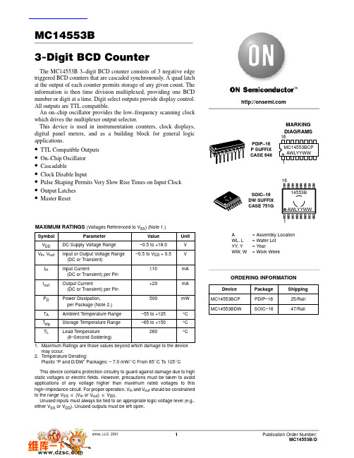
MC14553B3-Digit BCD CounterThe MC14553B 3–digit BCD counter consists of 3 negative edge triggered BCD counters that are cascaded synchronously. A quad latch at the output of each counter permits storage of any given count. The information is then time division multiplexed, providing one BCD number or digit at a time. Digit select outputs provide display control.All outputs are TTL compatible.An on–chip oscillator provides the low–frequency scanning clock which drives the multiplexer output selector.This device is used in instrumentation counters, clock displays,digital panel meters, and as a building block for general logic applications.•TTL Compatible Outputs •On–Chip Oscillator •Cascadable•Clock Disable Input•Pulse Shaping Permits Very Slow Rise Times on Input Clock •Output Latches •Master ResetMAXIMUM RATINGS (Voltages Referenced to V ) (Note 1.)may occur.2.Temperature Derating:Plastic “P and D/DW” Packages: – 7.0 mW/_C From 65_C To 125_C This device contains protection circuitry to guard against damage due to high static voltages or electric fields. However, precautions must be taken to avoid applications of any voltage higher than maximum rated voltages to this high–impedance circuit. For proper operation, V in and V out should be constrained to the range V SS v (V in or V out ) v V DD .Unused inputs must always be tied to an appropriate logic voltage level (e.g.,either V SS or V DD ). Unused outputs must be left open.DevicePackage Shipping ORDERING INFORMATIONMC14553BCP PDIP–1625/Rail MC14553BDWSOIC–1647/Rail查询CD4553 供应商Figure 1. Block Diagram121011139765142115V DD = PIN 16V SS = PIN 8TRUTH TABLE4.The formulas given are for the typical characteristics only at 25_C.5.To calculate total supply current at loads other than 50 pF:I T(C L) = I T(50 pF) + (C L – 50) Vfkwhere: I T is in µA (per package), C L in pF, V = (V DD – V SS) in volts, f in kHz is input frequency, and k = 0.004.7.Data labelled “Typ” is not to be used for design purposes but is intended as an indication of the IC’s potential performance.Figure 2. 3–Digit Counter Timing Diagram (Reference Figure 4)100099999899799699599499399299199090190089910110099989796959493929190898887861716151413121110987654321UNITS CLOCKUNITS Q0UNITS Q1UNITS Q2UNITS Q3TENS CLOCKTENS Q0TENS Q3HUNDREDSCLOCK HUNDREDS Q0HUNDREDS Q3DISABLE OVERFLOW MASTER RESET SCAN OSCILLATOR DIGIT SELECT 1DIGIT SELECT 2DIGIT SELECT 3LLOPERATING CHARACTERISTICSThe MC14553B three–digit counter, shown in Figure 4,consists of three negative edge–triggered BCD counters which are cascaded in a synchronous fashion. A quad latch at the output of each of the three BCD counters permits storage of any given count. The three sets of BCD outputs (active high), after going through the latches, are time division multiplexed, providing one BCD number or digit at a time. Digit select outputs (active low) are provided for display control. All outputs are TTL compatible.An on–chip oscillator provides the low frequency scanning clock which drives the multiplexer output selector.The frequency of the oscillator can be controlled externally by a capacitor between pins 3 and 4, or it can be overridden and driven with an external clock at pin 4. Multiple devices can be cascaded using the overflow output, which provides one pulse for every 1000 counts.The Master Reset input, when taken high, initializes the three BCD counters and the multiplexer scanning circuit.While Master Reset is high the digit scanner is set to digit one; but all three digit select outputs are disabled to prolong display life, and the scan oscillator is inhibited. The Disable input, when high, prevents the input clock from reaching the counters, while still retaining the last count. A pulse shaping circuit at the clock input permits the counters to continue operating on input pulses with very slow rise rmation present in the counters when the latch input goes high, will be stored in the latches and will be retained while the latch input is high, independent of other rmation can be recovered from the latches after the counters have been reset if Latch Enable remains high during the entire reset cycle.Figure 4. Expanded Block DiagramBCD OUTPUTS (ACTIVE HIGH)(ACTIVE HIGH)Figure 5. Six–Digit DisplayS T R O R E S C L O C K I N P U TD I S P L A Y S A RE L O W C U R R E N T L E D s(I p e a k < 10 m A P E R S E G M E N T )PDIP–16P SUFFIX PLASTIC DIP PACKAGENOTES:1.DIMENSIONING AND TOLERANCING PER ANSIY14.5M, 1982.2.CONTROLLING DIMENSION: INCH.3.DIMENSION L TO CENTER OF LEADS WHENFORMED PARALLEL.4.DIMENSION B DOES NOT INCLUDE MOLD FLASH.5.ROUNDED CORNERS OPTIONAL.MDIM MIN MAX MIN MAXMILLIMETERSINCHESA0.7400.77018.8019.55B0.2500.270 6.35 6.85C0.1450.175 3.69 4.44D0.0150.0210.390.53F0.0400.70 1.02 1.77G0.100 BSC 2.54 BSCH0.050 BSC 1.27 BSCJ0.0080.0150.210.38K0.1100.130 2.80 3.30L0.2950.3057.507.74M0 10 0 10S0.0200.0400.51 1.01____SOIC–16DW SUFFIX PLASTIC SOIC PACKAGE CASE 751G–03Notes11NotesON Semiconductor and are trademarks of Semiconductor Components Industries, LLC (SCILLC). SCILLC reserves the right to make changes without further notice to any products herein. SCILLC makes no warranty, representation or guarantee regarding the suitability of its products for any particular purpose, nor does SCILLC assume any liability arising out of the application or use of any product or circuit, and specifically disclaims any and all liability, including without limitation special, consequential or incidental damages. “Typical” parameters which may be provided in SCILLC data sheets and/or specifications can and do vary in different applications and actual performance may vary over time. All operating parameters, including “Typicals” must be validated for each customer application by customer’s technical experts. SCILLC does not convey any license under its patent rights nor the rights of others.SCILLC products are not designed, intended, or authorized for use as components in systems intended for surgical implant into the body, or other applications intended to support or sustain life, or for any other application in which the failure of the SCILLC product could create a situation where personal injury or death may occur. Should Buyer purchase or use SCILLC products for any such unintended or unauthorized application, Buyer shall indemnify and hold SCILLC and its officers, employees, subsidiaries, affiliates, and distributors harmless against all claims, costs, damages, and expenses, and reasonable attorney fees arising out of, directly or indirectly, any claim of personal injury or death associated with such unintended or unauthorized use, even if such claim alleges that SCILLC was negligent regarding the design or manufacture of the part. SCILLC is an Equal Opportunity/Affirmative Action Employer. PUBLICATION ORDERING INFORMATIONCENTRAL/SOUTH AMERICA:Spanish Phone:303–308–7143 (Mon–Fri 8:00am to 5:00pm MST)Email:ONlit–spanish@Toll–Free from Mexico: Dial 01–800–288–2872 for Access –then Dial 866–297–9322ASIA/PACIFIC: LDC for ON Semiconductor – Asia SupportPhone:303–675–2121 (Tue–Fri 9:00am to 1:00pm, Hong Kong Time)Toll Free from Hong Kong & Singapore:001–800–4422–3781Email: ONlit–asia@JAPAN: ON Semiconductor, Japan Customer Focus Center4–32–1 Nishi–Gotanda, Shinagawa–ku, Tokyo, Japan 141–0031Phone: 81–3–5740–2700。
双通道低成本模数转换器cs5550中文
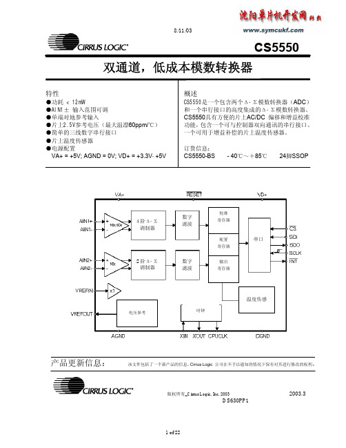
4 寄存器描述…………………………………………………………………………..…………………..18 4.1 配置寄存器………………………………………………………………………………...18 4.2 DC偏移寄存器…………………………………………………………………………...19 4.3 AC/DC增益寄存器……………………………………………………………………..19 4.4 周期计数寄存器…………………………………………………………………………...19 4.5 输出寄存器………………………………………………………………………………...20 4.6 滤波输出寄存器…………………………………………………………………………...20 4.7 状态寄存器和屏蔽寄存器………………………………………………………………...20 4.8 AC偏移寄存器…………………………………………………………………………...21 4.9 温度传感器数据输出寄存器………………………...……………………………………21 4.10 控制寄存器………………………………………………………………………………...21
4 of 22
8/11/03
1. 特性与规格说明 . 最大值和最小值参数是指在所有的操作条件可被保证的值.
. 典型参数是在标准供电和25°C时的测量值. . DGND = 0V.所有电压是指对 0V 的电压值.
模拟特性
参数
符号 最小值
精度(两个通道)
共模抑制比
CMRR
80
偏移漂移
-
模拟输入(AIN1±) 差分输入范围 {(AIN1+) - (AIN1- )}
测量和参考输入
差分模拟输入9,10,15,16 AIN1+, AIN1-, AIN2+, AIN2- —差分模拟输入引脚。
DS91M125 125 MHz 1 4 M-LVDS Repeater with LVDS Inp
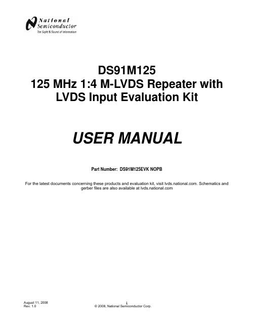
DS91M125 125 MHz 1:4 M-LVDS Repeater withLVDS Input Evaluation KitUSER MANUALPart Number: DS91M125EVK NOPBFor the latest documents concerning these products and evaluation kit, visit . Schematics andgerber files are also available at OverviewThe purpose of this document is to familiarize you with the DS91M125 evaluation board, suggest the test setup procedures and instrumentation, and to guide you through some typical measurements that will demonstrate the performance of the device. The board enables the user to examine performance and all functions of theDS91M125 as a standalone device.The DS91M125 is a high-speed 1:4 M-LVDS repeater with an LVDS input designed for multipoint applications with multiple drivers or receivers. The device conforms to TIA/EIA-899 standard. It utilizes M-LVDS technology for low power, high-speed and superior noise immunity.DescriptionFigure 1 below represents the top layer drawing of the board with the silkscreen annotations. It is a 2.5 x 3 inch 4 layer printed circuit board (PCB) that features a single DS91M125 (U2) device.Figure 1 -DS91M125EVK Top View DrawingDS91M125 Evaluation in a Point-to-Point LinkThe following is a recommended procedure for using and evaluating the DS91M125EVK. Figure 2 depicts a typical setup and instrumentation used.1. Select a single DS91M125 evaluation board.2. Apply the power to the board (3.3 V typical) between J3 and J4 power tabs, observe the value of I CC,and compare it with the expected value (refer to the datasheet) to ensure that the devices arefunctional.3. Enable one of the U2 driver outputs. This is accomplished by setting the DE0-3 pin to VDD (JP3-6).4. Connect a signal source to the driver input (DI+, DI-). The signal needs to be an LVDS/M-LVDS/CML/LVPECL compliant signal. Refer to the DS91M125 datasheet for the receiver inputcompatibility.5. Connect one of the U2 outputs (A0-3/B0-3) to an oscilloscope and observe the waveforms.Figure 2 – DS91M125 Test SetupFigure 3 shows an eye diagram acquired at the output of the DS91M125 driver loaded with a 100-ohm resistor. The generator connected to the driver input simulated a 100 Mbps PRBS-7 NRZ.Figure 3 – DS91M125 OutputIMPORTANT NOTICETexas Instruments Incorporated and its subsidiaries(TI)reserve the right to make corrections,modifications,enhancements,improvements, and other changes to its products and services at any time and to discontinue any product or service without notice.Customers should obtain the latest relevant information before placing orders and should verify that such information is current and complete.All products are sold subject to TI’s terms and conditions of sale supplied at the time of order acknowledgment.TI warrants performance of its hardware products to the specifications applicable at the time of sale in accordance with TI’s standard warranty.Testing and other quality control techniques are used to the extent TI deems necessary to support this warranty.Except where mandated by government requirements,testing of all parameters of each product is not necessarily performed.TI assumes no liability for applications assistance or customer product design.Customers are responsible for their products and applications using TI components.To minimize the risks associated with customer products and applications,customers should provide adequate design and operating safeguards.TI does not warrant or represent that any license,either express or implied,is granted under any TI patent right,copyright,mask work right, or other TI intellectual property right relating to any combination,machine,or process in which TI products or services are rmation published by TI regarding third-party products or services does not constitute a license from TI to use such products or services or a warranty or endorsement e of such information may require a license from a third party under the patents or other intellectual property of the third party,or a license from TI under the patents or other intellectual property of TI.Reproduction of TI information in TI data books or data sheets is permissible only if reproduction is without alteration and is accompanied by all associated warranties,conditions,limitations,and notices.Reproduction of this information with alteration is an unfair and deceptive business practice.TI is not responsible or liable for such altered rmation of third parties may be subject to additional restrictions.Resale of TI products or services with statements different from or beyond the parameters stated by TI for that product or service voids all express and any implied warranties for the associated TI product or service and is an unfair and deceptive business practice.TI is not responsible or liable for any such statements.TI products are not authorized for use in safety-critical applications(such as life support)where a failure of the TI product would reasonably be expected to cause severe personal injury or death,unless officers of the parties have executed an agreement specifically governing such use.Buyers represent that they have all necessary expertise in the safety and regulatory ramifications of their applications,and acknowledge and agree that they are solely responsible for all legal,regulatory and safety-related requirements concerning their products and any use of TI products in such safety-critical applications,notwithstanding any applications-related information or support that may be provided by TI.Further,Buyers must fully indemnify TI and its representatives against any damages arising out of the use of TI products in such safety-critical applications.TI products are neither designed nor intended for use in military/aerospace applications or environments unless the TI products are specifically designated by TI as military-grade or"enhanced plastic."Only products designated by TI as military-grade meet military specifications.Buyers acknowledge and agree that any such use of TI products which TI has not designated as military-grade is solely at the Buyer's risk,and that they are solely responsible for compliance with all legal and regulatory requirements in connection with such use. TI products are neither designed nor intended for use in automotive applications or environments unless the specific TI products are designated by TI as compliant with ISO/TS16949requirements.Buyers acknowledge and agree that,if they use any non-designated products in automotive applications,TI will not be responsible for any failure to meet such requirements.Following are URLs where you can obtain information on other Texas Instruments products and application solutions:Products ApplicationsAudio /audio Automotive and Transportation /automotiveAmplifiers Communications and Telecom /communicationsData Converters Computers and Peripherals /computersDLP®Products Consumer Electronics /consumer-appsDSP Energy and Lighting /energyClocks and Timers /clocks Industrial /industrialInterface Medical /medicalLogic Security /securityPower Mgmt Space,Avionics and Defense /space-avionics-defense Microcontrollers Video and Imaging /videoRFID OMAP Mobile Processors /omapWireless Connectivity /wirelessconnectivityTI E2E Community Home Page Mailing Address:Texas Instruments,Post Office Box655303,Dallas,Texas75265Copyright©2012,Texas Instruments Incorporated。
CS5351-DZZ中文资料
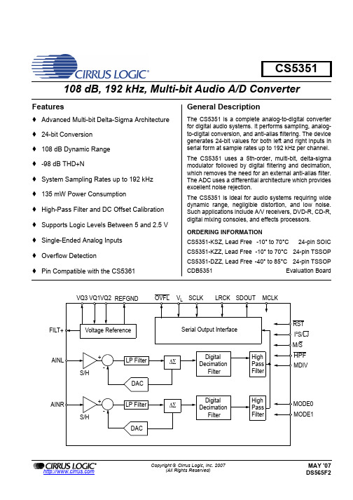
General Description
The CS5351 is a complete analog-to-digital converter for digital audio systems. It performs sampling, analogto-digital conversion, and anti-alias filtering. The device generates 24-bit values for both left and right inputs in serial form at sample rates up to 192 kHz per channel.
4.1 Operational Mode/Sample Rate Range Select .............................................................................. 16 4.2 System Clocking ............................................................................................................................ 16
MIC3202 MIC3202-1 LED驱动器评估板说明书
MIC3202/MIC3202-1Evaluation BoardHigh-Brightness LED Driver with IntegratedMOSFET and High-Side Current Sense Micrel Inc. • 2180 Fortune Drive • San Jose, CA 95131 • USA • tel +1 (408) 944-0800 • fax + 1 (408) 474-1000 • General DescriptionThe MIC3202/MIC3202-1 is a hysteretic step-down,constant-current, High-Brightness LED (HB LED) driver.It provides an ideal solution for interior/exterior lighting,architectural and ambient lighting, LED bulbs, and othergeneral illumination applications.This board enables the evaluation of theMIC3202/MIC3202-1 for 1A LED current. The board isoptimized for ease of testing, with all the components ona single side. The device operates from a 6V to 37Vinput voltage range, and includes an integrated 1.0AMOSFET. When the input voltage approaches andcrosses UVLO threshold, the internal 5V V CC isregulated and the integrated MOSFET is turned on if ENpin and DIM pin are high. The inductor current builds uplinearly. When the CS pin voltage hits the V CS(MAX) withrespect to V IN,the internal MOSFET is turned off and theSchottky diode takes over and returns the current to V IN.Then the current through inductor and LEDs startsdecreasing. When CS pin hits V CS(MIN), the internalMOSFET is turned on and the cycle repeats.Since the control scheme does not need loopcompensation, it makes for a very simple design andavoids problems of instability.Datasheets and support documentation can be found onMicrel’s web site at: .RequirementsThis board needs a single-bench power sourceadjustable over the input voltage of 6V < V IN < 37V thatcan provide at least 1A of current. The loads can eitherbe active (electronic load in CV mode) or passive(LEDs) with the ability to dissipate the maximum loadpower while keeping accessible surfaces ideally <70°C.PrecautionsThere is no reverse input protection on this board. Whenconnecting the input sources, ensure that the correctpolarity is observed.In the line transient condition, such as hot plug-in, anelectrolytic capacitor may be required at the VIN andGND terminals in order to prevent IC damage from asurge voltage.Getting Started1. Connect V IN supply to the input VIN and GNDterminals. With the output of this supply disabled,set the supply voltage to the desired input testvoltage (6V < V IN < 37V). This supply voltage shouldbe monitored at the test boards input terminals toallow voltage drops in the test cables (and ammeterif used) to be accounted for. An ammeter can beadded inline with the +VIN input terminal toaccurately measure input current.2. Connect the LEDs to the output terminalsbetween LED+ and LED−. This LED voltage dropdepends on manufacturer tolerance and number ofLEDs. The LED current can be measured using anammeter or current probe. A 4.7µF ceramiccapacitor helps to reduce the current ripple throughthe LED. The LED current is set to 1A by a 200mΩcurrent-sense resistor (R CS).3. Enable the input supply. By default, the IC isenabled when the input voltage crosses the VINthreshold (4V) and the internal VCC regulator andinternal MOSFET are turned on with the EN andDIM pins are high. To use the EN and DIM functionsof the MIC3202/MIC3202-1, a test point is providedfor each of them.Ordering InformationPart Number DescriptionMIC3202YME EV MIC3202YME Evaluation BoardOther FeaturesEN InputThe EN pin provides a logic level control of the output and the voltage has to be 2.0V or higher to enable the current regulator. The output stage is gated by the DIM pin. When the EN pin is pulled low, the regulator goes to off-state and the supply current of the device is reduced to below 1µA. Do not drive the EN pin above the supply voltage. DIM InputThe DIM pin provides a logic level control for brightness of the LED. A PWM input can be used to control the brightness of LED. DIM high enables the output and its voltage has to be 2.0V or higher. DIM low disables the output, regardless of EN high-state. Current-Sense InputThe CS pin provides the high-side current sense to set the LED current with an external sense resistor.A sense resistor R CS is placed between V IN and LED+ terminals.The current through LED is sensed by the sense resistor (R CS ). The sensed voltage is fed back to the MIC3202 to regulate the LED current R CS is given by:)I V +V (x 21=R LED)MIN (CS )MAX (CS CS Error!Bookmark not defined.I LED is LED current required to set.R CS (Ω) I LED (A)I 2R (W)Size (SMD)1.33 0.15 0.03 0603 0.56 0.35 0.07 0805 0.4 0.5 0.1 0805 0.28 0.7 0.137 0805 0.2 1.0 0.2 1206For V CS(MAX) and V CS(MIN) refers to the Electrical Characteristics table. Frequency of OperationTo calculate the frequency spread across input supply:)V +V (×I Δ×L )V R ×I V (×)V +R ×I +V (=F IN D L LED CS LED IN LED CS LED D SW --CS)MIN (CS )MAX (CS L R V V =I Δ-where:V D is Schottky diode forward drop V LED is total LEDs voltage drop V IN is input voltageI LED is average LED currentAccording to the above equation, choose the inductor to make the operating frequency no higher than 1MHz.Refer to the datasheet Application Information for more information on components selection guidelines. Frequency DitheringThe MIC3202 is designed to modulate the V CS(MAX) with amplitude ±6mV by a pseudo random generator to generate the ±12% of the switching frequency dithering. This spreads the frequency spectrum over a wider range and reduce the EMI noise peaks.The MIC3202-1 is non-dithering version of the MIC3202.Notes:1. If bulk capacitor on input rail is away (4 inches or more) from the MIC3202/MIC3202-1, install the 100µF bulk capacitor near V IN.2. Source impedance should be as low as 10mΩ.Bill of MaterialsItem Part Number Manufacturer DescriptionQty. 12105C475KAZ2A AVX (1) C1, C2, C8GRM32ER71H475KA88L Murata (2) 4.7µF/50V, Ceramic Capacitor, X7R, Size 1210 2 08053D105KAT2A AVX (1)1µF/25V, Ceramic Capacitor, X5R, Size 0805 1 GRM21BR71E105KA99L Murata (2) C3, C9C2012X7R1E105K TDK (3)1µF/25V, Ceramic Capacitor, X7R, Size 0805 1 06035C271KAT2A AVX (1)C4, C7GRM188R71H271KA01D Murata (2)270pF/50V, Ceramic Capacitor NPO, Size 0603206035C104MAT AVX (1)GRM188R71H104KA93D Murata (2) C5, C6C1608X7R1H104K TDK (3)0.1µF/50V, Ceramic Capacitor, X7R, Size 06032SS24-TP MCC (4) D1 SS24 Fairchild (5) 60V, 2A, SMA, Schottky Diode 1 D2, D3B0530WS-TPMCC (4) 30V, 200mA, Schottky diode, SOD-323 2 L1 SLF10145T-470M1R4 TDK (3) 47µH, 1.4A, SMT, Power Inductor 1 R1 CSR 1/2 0.2 1% I Stackpole Electronics,Inc (7)0.2Ω Resistor, 1/2W, 1%, Size 12061 R2, R3CRCW06031003FKEAVishay (8) 100k Ω Resistor, 1%, Size 06032 R4 CRCW08052R20FKEA Vishay (8) 2.2Ω Resistor, 1%, Size 0805 1 R5 CRCW080510R0FKEA Vishay (8) 10Ω Resistor, 1%, Size 0805 1 R6 CRCW060310K0FKEA Vishay (8) 10k Ω Resistor, 1%, Size 0603 1 R7, R8CRCW06030000FKEAVishay (8)0Ω Resistor, 1%, Size 06032 R9 CRCW060349R9FKEA Vishay (8)49.9Ω Resistor, 1%, Size 0603 1RV1 3386P-1-104TLF Bourns (9) POT 100k Ω 3/8" SQ CERM SL ST1U1 MIC3202YME Micrel, Inc.(10)High Brightness LED Driver with High-SideCurrent Sense 1 U2 MIC1557YM5Micrel, Inc.(10) RC Time/Oscillator (SOT-23-5)1Notes:1. AVX: .2. Murata: .3. TDK: .4. MCC: .5. Fairchild: .6.Diodes Inc. : .7. Stackpole Electronics: . 8. Vishay: . 9.Bourns Inc : . 10. Micrel, Inc.: .PCB Layout RecommendationsTop AssemblyTop LayerPCB Layout Recommendations (Continued)Bottom Layer。
MCF5307 ColdFire集成微处理器的SDRAM控制器应用注意事项说明书
Consumer Technologies GroupOrder this document byAN1766/D REV 2.0Application NoteUsing the SDRAM Controller on the MCF5307 ColdFire ¨ Integrated MicroprocessorAN1766INTRODUCTIONThereÕs a new type of memory thatÕs becoming very popular in systems designs. ItÕs called synchronous DRAM (SDRAM), and itspecifically supports the high-speed bus designs required to fully utilize current high-performance microprocessors. The MCF5307 ColdFire¨ integrated microprocessor is the first of the ColdFire Family to contain the Version 3 clock-doubled core. The MCF5307 SDRAM controller can interface with over 2,000 MBytes of DRAM and supports bursting and page-mode operations. In addition, the SDRAM controller can connect to both extended-data-out DRAMs and synchronous DRAMs.Running synchronously with the system clock rather than responding to traditionalasynchronous control signals, SDRAM can (after an initial latency period) be read or written on every clock cycle. A 5-1-1-1 burst rate is typical at 100 MHz. To support interleaving, many SDRAM devices contain multiple banks and all banks can have an open page at any time. DRAMs use a multiplexed address bus in which the processor provides the address in two cycles. The most significant portion of the address is transmitted first (the row), followed by the lowerportion (the column). Gated by the system clock, the row and column are latched by the DRAM and together form the complete address required to identify the requested data. The multiplexing reduces the pin count of the packages as well as the number of pad connections on the chip, and so lowers the memory cost. The trade-off for this pin count and memory reduction is slower performance because it mandates an additional cycle to transmit the address. Memory designers have developed new interfaces to reduce the impact of this trade-off. One example is page-mode operation. Page mode sends the rowaddress portion only once for multiple accesses within a memory region (a page). The newest concept is SDRAM, which can accept new column addresses on every system clock cycle and, after an initial pipeline latency period, deliver or receive data at the same rate.SDRAM controllers require a higher level of sophistication than asynchronous DRAMcontrollers. Not only must addresses and data be managed, but SDRAM chips also need special ÒcommandsÓ to be sent from the controller to initialize the memory as well as to instruct the memory which operations are to occur. These commands include instructions to precharge, read, write, burst, auto-refresh, and variousscale Semiconductorconductor, Inc., 2004. All rights reserved.F r e e s c a l e S e m i c o n d u c t o r , IFreescale Semiconductor, Inc.n c .F r e e s c a l e S e m i c o n d u c t o r , IFreescale Semiconductor, Inc.n c .F r e e s c a l e S e m i c o n d u c t o r , IFreescale Semiconductor, Inc.n c .F r e e s c a l e S e m i c o n d u c t o r , IFreescale Semiconductor, Inc.n c .F r e e s c a l e S e m i c o n d u c t o r , IFreescale Semiconductor, Inc.n c .F r e e s c a l e S e m i c o n d u c t o r , IFreescale Semiconductor, Inc.n c .SPECIAL CONSIDERATIONSIt is important to be aware of the designassumptions that are built in to the controller. As part of the design process, certain parameters must be constrained in order to produce an efficient and reliable controller. These determine how the controller will operate in specific circumstances. Some of these conditions are listed below:RESET State - Following a reset of the MCF5307 processor the SADRAMC isdisabled. It must be initialized before operation can begin.Fixed Page Size - The controller on the MCF5307 is hard-configured for a 512-byte page (column) size. Should memories with larger page sizes be used, the controller will treat any access outside of a 512-byte boundary as a new page. As such, it will ÒcloseÓ the current page and issue a new row address for the new page.No Mixed Memory Types - The default (out of RESET) mode of operation for the MCF5307 assumes asynchronous DRAMs. This default can be changed by setting the SO bit (bit 15) to a Ò1Ó in the DRAM Control Register on theMCF5307. Once synchronous operation is set, it cannot be reversed except by resetting the MCF5307. Both banks will operate in the selected mode. Mixing asynchronous andsynchronous DRAMs is not allowed. Each bank can contain a unique configuration of SDRAM. That is, the speeds, port widths, etc. may be different in each of the two banks.External Master Multiplexing - While theMCF5307 SADRAMC will respond to SDRAM accesses by alternate bus masters, it will not drive the address lines to provide address multiplexing when this occurs. The controller will drive the appropriate control signals only. Addresses must, in this case, be externally multiplexed if required.Bursting - Many SDRAMS can burst data in various amounts; however, the controller on the MCF5307 does not support this feature. The controller will instead conduct all accesses by directly controlling the address lines. Therefore, if variable-length bursting is available on the chosen SDRAM, the burst option must not be enabled, or the burst length must be set to one. This was done in the setting of the Mode Register in the first example.EDGESEL - The synchronous edge-select input pin on the MCF5307 can provide additional output hold time for the SDRAM control signals. The usual mode of operation is to use a buffer that slightly delays the BCLKO signal. This delayed signal is then routed to the SDRAM and back to the EDGESEL pin on the MCF5307. This will have the effect of holding the signals to the SDRAM by the amount of buffer and line delay, which helps to ensure that data are held beyond the falling edge of the SDRAM clock input signal. This is a useful feature with regard to meeting memory system timing requirements on high-frequency buses.Asymmetrical Memory Devices - Whenasymmetrical memory devices are used (i.e. the memory chips have more row addresses than column addresses), the additional row addresses will be connected by using sequential MCF5307 pins until done. That is, physical pins will not be skipped. Additionally, for 32 bit ports with only eight column addresses, or 8-bit ports with just nine columns, MCF5307 pin A18 can be used to provide SDRAM row address 18 even though it is noted for 16-bit port use only. Likewise for 16-bit ports with eight column address signals, MCF5307 address pin 17 may be used to provide SDRAM row address 17.F r e e s c a l e S e m i c o n d u c t o r , In c .Revision History: Rev. 1.0 - Initial ReleaseRev 2.0 - Corrected maximum size of accessible memory. Moved note, in expanded form, from the bottom of the Generic Address Connection Scheme table on page three to text in the SpecialConsiderations section. Corrected calculation of RC Field value in SDRAM Initialization section. Heavily revised description of mode register load procedure to correct errors in rev 1.0. Fixed miscellaneous typos.F r e e s c a l e S e m i c o n d u c t o r , In c .How to Reach Us:Home Page:E-mail:*********************USA/Europe or Locations Not Listed: Freescale SemiconductorTechnical Information Center, CH370 1300 N. Alma School Road Chandler, Arizona 85224+1-800-521-6274 or +1-480-768-2130 *********************Europe, Middle East, and Africa:Freescale Halbleiter Deutschland GmbH Technical Information Center Schatzbogen 781829 Muenchen, Germany +44 1296 380 456 (English) +46 8 52200080 (English) +49 89 92103 559 (German) +33 1 69 35 48 48 (French) *********************Japan:Freescale Semiconductor Japan Ltd. Headquarters ARCO Tower 15F1-8-1, Shimo-Meguro, Meguro-ku, Tokyo 153-0064 Japan0120 191014 or +81 3 5437 9125 ***************************Asia/Pacific:Freescale Semiconductor Hong Kong Ltd. Technical Information Center 2 Dai King StreetTai Po Industrial Estate Tai Po, N.T., Hong Kong +800 2666 8080**************************For Literature Requests Only:Freescale Semiconductor Literature Distribution Center P.O. Box 5405Denver, Colorado 802171-800-441-2447 or 303-675-2140 Fax: 303-675-2150*********************************************Information in this document is provided solely to enable system and software implementers to use Freescale Semiconductor products. There are no express or implied copyright licenses granted hereunder to design or fabricate any integrated circuits or integrated circuits based on the information in this document.Freescale Semiconductor reserves the right to make changes without further notice to any products herein. Freescale Semiconductor makes no warranty, representation or guarantee regarding the suitability of its products for any particular purpose, nor does Freescale Semiconductor assume any liability arising out of the application or use of any product or circuit, and specifically disclaims any and all liability, including without limitation consequential or incidental damages. “Typical” parameters which may be provided in Freescale Semiconductor data sheets and/or specifications can and do vary in different applications and actual performance may vary over time. All operating parameters, including “Typicals” must be validated for each customer application by customer’s technical experts. Freescale Semiconductor does not convey any license under its patent rights nor the rights of others. Freescale Semiconductor products are not designed, intended, or authorized for use as components in systems intended for surgical implant into the body, or other applications intended to support or sustain life, or for any other application in which the failure of the Freescale Semiconductor product could create a situation where personal injury or death may occur. Should Buyer purchase or use Freescale Semiconductor products for any such unintended or unauthorized application, Buyer shall indemnify and hold Freescale Semiconductor and its officers, employees, subsidiaries, affiliates, and distributors harmless against all claims, costs, damages, and expenses, and reasonable attorney fees arising out of, directly or indirectly, any claim of personal injury or death associated with such unintended or unauthorized use, even if such claim alleges that Freescale Semiconductor was negligent regarding the design or manufacture of the part.。
ds3553 规格书
4.1.
I2C 地址......................................................................................................................................................6
6.2.5. STEP_CNT_H 寄存器(C6H) ...............................................................................................................10
7. 封装尺寸图..............................................................................................................................................................11
3.1.
极限参数 ....................................................................................................................................................5
4. I2C 通讯接口..............................................................................................................................................................6
晶华微电子 SD2085 低功耗 HART 调制解调器说明书
CMOS时钟典型连接如图9所示,将XCEN 置为高电平,并将3.6864MHz外部时钟源连至 XTAL1引脚,而XTAL2引脚保持开路状态。
晶华微电子 版本 v0
2015/5
3.6864MHz DVDD
XTAL1
SD2085
XTAL2 XCEN
图9.外灌CMOS时钟连接
STOP
时钟配置
SD2085提供两种时钟配置选项:外部晶振 和CMOS时钟输入。
外部晶振的典型连接如图8所示,将XCEN 置为低电平,晶振采用3.6864MHz.。晶振和电 容应尽量靠近SD2085。
C1
8pF 3.6864 MHz 8pF
C2
XTAL1
SD2085
XTAL2 XCEN
图8.晶振连接
图 3. HART FSK 信号
FSK 调制器
当RTSb信号设为低电平,SD2085处于发 送模式,调制器通过波形整形电路,将D_IN输 入端的非归零制(NRZ)数字信号,转换成一系 列1200Hz和2200Hz符合HART协议要求、相位
SD2085
FSK_OUT 22nF
2.2µF
RLOAD
图5. FSK_OUT驱动阻性负载
SD2085 低功耗 HART 调制解调器
特点
z 单芯片、半双工 1200bps FSK 调制解调器 z 符合 HART 通信协议物理层要求 z 符合 Bell202 标准载波 1200Hz 和 2200Hz z HART 波形整形输出具有额外驱动能力 z 数字信号处理确保可靠的输入信号检测 z UART 接口 z 工作电压 2.7V~3.6V z 低功耗,调制模式下最大功耗为 85μA z -55℃至+125℃工作温度范围 z 20 引脚 5mm x 5mm x 0.75mm TQFN 封装 z 满足 RoHS 环保要求
DS-1C型程控失真度检定装置 使用说明书
DS-1C型程控失真度检定装置使用说明书中国计量科学研究院北京凯弘电子仪器有限公司2014年3月目录一、概述----------------------------------------------------------3二、主要技术指标----------------------------------------------3三、工作原理----------------------------------------------------51.整机方框图-------------------------------------------52.标准失真波信号的形成----------------------------53.标准不平衡电压的产生----------------------------64.主要单元电路简介------------------------------------7四、面板按钮和功能-------------------------------------------8五、使用方法----------------------------------------------------91.开机状态--------------------------------------------------92.检定失真仪-----------------------------------------------103.基波谐波输出电压设置及校-------------------------104.标准失真波电压设置及校准-------------------------115.校准电压表频响校准---------------------------------116.校准操作注意事项------------------------------------12六、程控操作指南---------------------------------------------12七、注意事项---------------------------------------------------15一、概述DS-1C型程控失真度检定装置是一种输出频率范围由5Hz至200kHz的高精度标准失真波信号发生器。
BP2833A_CN_DS_Rev.1.0

非隔离降压型 LED 恒流驱动芯片
6) (无特别说明情况下,VCC =15 V, TA =25 ℃) 描述 条件 最小值 典型值 最大值 单位
注 5:典型参数值为 25˚C 下测得的参数标准。 注 6:规格书的最小、最大规范范围由测试保证,典型值由设计、测试或统计分析保证。
BP2833A_CN_DS_Rev.1.0
JA
推荐工作范围(注 4)
符号 ILED 1 ILED 2 VLED min 参数 输出 LED 电流@ Vout=72V (输入电压 176V~265V) 输出 LED 电流@ Vout=36V (输入电压 176V~265V) 最小负载 LED 电压 参数范围 280 350 >15 单位 mA mA V
BP2833A
晶丰明源半导体
定购信息
定购型号 BP2833A 封装 SOP8 温度范围 -40 ℃到 105 ℃ 2,500 颗/盘 包装形式 编带 打印 BP2833A XXXXXY WWXYY
非隔离降压型 LED 恒流驱动芯片
管脚封装
GND CDRAIN DRAIN
前沿消隐
+
电流检测
CS
400mV
ROVP
GND
图 3 BP2833A 内部框图
应用信息
BP2833A 是一款专用于 LED 照明的恒流驱动芯片, 应用于非隔离降压型 LED 驱动电源。采用专利的 恒流架构和控制方法,芯片内部集成 500V 功率开 关,只需要极少的外围组件就可以达到优异的恒 流特性。而且无需辅助绕组供电和检测,系统成 本极低。 启动 系统上电后,母线电压通过启动电阻对 VCC 电容充 电,当 VCC 电压达到芯片开启阈值时,芯片内部控 制电路开始工作。BP2833A 内置 17V 稳压管,用于 钳位 VCC 电压。 芯片正常工作时, 需要的 VCC 电流极 低,所以无需辅助绕组供电。 恒流控制,输出电流设置 芯片逐周期检测电感的峰值电流,CS 端连接到内 部的峰值电流比较器的输入端,与内部 400mV 阈
R328硬件设计指南V1.0-20190418
1.6. Flash 电路设计............................................................................................................................................ 14
市研读慧科者技有对限 象
市研慧科技有限
深圳 本文档主要适用于: 深圳
硬件开发工程师
软件开发工程师
技术支持工程师
公司Yanhui 市研慧科技有限 深圳
公司Yanhui 市研慧科技有限 深圳
公 市研慧科技有限 深圳
公司Yanhui 市研慧科技有限 深圳
公司Yanhui 市研慧科技有限 深圳
公司Yanhui 市研慧科技有限 深圳
目录.................................................................................................................................................................................3
1.3.3. 上电时序设计................................................................................................................................ 13
1.4. 复位电路设计............................................................................................................................................ 14
CS5532-BSZR;CS5534-BSZR;CDB5532U;中文规格书,Datasheet资料

Copyright © Cirrus Logic, Inc. 2008CS5532/34-BS24-bit ∆Σ ADCs with Ultra-low-noise PGIAFeaturesChopper-stabilized PGIA (ProgrammableGain Instrumentation Amplifier, 1x to 64x)– 6 nV/√Hz @ 0.1 Hz (No 1/f noise) at 64x –1200pA Input Current with Gains >1 Delta-sigma Analog-to-digital Converter –Linearity Error: 0.0007% FS–Noise-free Resolution: Up to 23 bits Two- or Four-channel Differential MUX Scalable Input Span via Calibration –±5 mV to differential ±2.5VScalable V REF Input: Up to Analog Supply Simple Three-wire Serial Interface –SPI™ and Microwire™ Compatible –Schmitt Trigger on Serial Clock (SCLK) R/W Calibration Registers Per Channel Selectable Word Rates: 6.25 to 3,840 Sps Selectable 50 or 60 Hz RejectionPower Supply Configurations–VA+ = +5 V; VA- = 0 V; VD+ = +3 V to +5 V–VA+ = +2.5 V; VA- = -2.5 V; VD+ = +3 V to +5 V –VA+ = +3 V; VA- = -3 V; VD+ = +3 VGeneral DescriptionThe CS5532/34 are highly integrated ∆Σ Analog-to-Digi-tal Converters (ADCs) which use charge-balance techniques to achieve 24-bit performance. The ADCs are optimized for measuring low-level unipolar or bipolar signals in weigh scale, process control, scientific, and medical applications.To accommodate these applications, the ADCs come as either two-channel (CS5532) or four-channel (CS5534)devices and include a very low-noise, chopper-stabilized instrumentation amplifier (6 nV/√Hz @ 0.1 Hz) with se-lectable gains of 1×, 2×, 4×, 8×, 16×, 32×, and 64×.These ADCs also include a fourth-order ∆Σ modulator followed by a digital filter which provides twenty selectable output word rates of 6.25, 7.5, 12.5, 15, 25, 30, 50, 60, 100,120, 200, 240, 400, 480, 800, 960, 1600, 1920, 3200, and 3840 Sps (MCLK =4.9152MHz).To ease communication between the ADCs and a micro-controller, the converters include a simple three-wire se-rial interface which is SPI™ and Microwire™ compatible with a Schmitt-trigger input on the serial clock (SCLK).High dynamic range, programmable output rates, and flexible power supply options makes these ADCs ideal solutions for weigh scale and process control applications.ORDERING INFORMATIONSee page 47VA+C1C2VREF+VREF-VD+DIFFERENTIAL 4TH ORDER ∆ΣMODULATORPGIA 1,2,4,8,16PROGRAMMABLE SINC FIR FILTERMUX(CS5534SHOWN)AIN1+AIN1-AIN2+AIN2-AIN3+AIN3-AIN4+AIN4-SERIAL INTERFACELATCHCLOCK GENERATORCALIBRATION SRAM/CONTROLLOGICDGNDCSSDI SDO SCLKOSC2OSC1A1A0/GUARD VA-32,64OCT ‘08TABLE OF CONTENTS1.CHARACTERISTICS AND SPECIFICATIONS (4)ANALOG CHARACTERISTICS (4)TYPICAL RMS NOISE (NV) (7)TYPICAL NOISE-FREE RESOLUTION(BITS) (7)5 V DIGITAL CHARACTERISTICS (8)3 V DIGITAL CHARACTERISTICS (8)DYNAMIC CHARACTERISTICS (9)ABSOLUTE MAXIMUM RATINGS (9)SWITCHING CHARACTERISTICS (10)2.GENERAL DESCRIPTION (12)2.1.Analog Input (12)2.1.1. Analog Input Span (13)2.1.2. Multiplexed Settling Limitations (13)2.1.3. Voltage Noise Density Performance (13)2.1.4. No Offset DAC (14)2.2.Overview of ADC Register Structure and Operating Modes (14)2.2.1. System Initialization (15)2.2.2. Serial Port Interface (22)2.2.3. Reading/Writing On-Chip Registers (23)2.3.Configuration Register (23)2.3.1. Power Consumption (23)2.3.2. System Reset Sequence (23)2.3.3. Input Short (24)2.3.4. Guard Signal (24)2.3.5. Voltage Reference Select (24)2.3.6. Output Latch Pins (24)2.3.7. Offset and Gain Select (25)2.3.8. Filter Rate Select (25)2.4.Setting up the CSRs for a Measurement (27)2.5.Calibration (30)2.5.1. Calibration Registers (30)2.5.2. Performing Calibrations (31)2.5.3. Self Calibration (31)2.5.4. System Calibration (32)2.5.5. Calibration Tips (32)2.5.6. Limitations in Calibration Range (33)2.6.Performing Conversions (33)2.6.1. Single Conversion Mode (33)2.6.2. Continuous Conversion Mode (34)2.6.3. Examples of Using CSRs to Perform Conversions and Calibrations (35)ing Multiple ADCs Synchronously (36)2.8.Conversion Output Coding (36)2.9.Digital Filter (38)2.10.Clock Generator (39)2.11.Power Supply Arrangements (39)2.12.Getting Started (43)2.13.PCB Layout (43)3.PIN DESCRIPTIONS (44)4.SPECIFICATION DEFINITIONS (46)5.ORDERING INFORMATION (47)6.ENVIRONMENTAL, MANUFACTURING, & HANDLING INFORMATION (47)7.PACKAGE DRAWINGS (48)LIST OF FIGURESFigure 1. SDI Write Timing (Not to Scale) (11)Figure 2. SDO Read Timing (Not to Scale) (11)Figure 3. Multiplexer Configuration (12)Figure 4. Input models for AIN+ and AIN- pins (13)Figure 5. Measured Voltage Noise Density (13)Figure 6. CS5532/34 Register Diagram (14)Figure 7. Command and Data Word Timing (22)Figure 8. Guard Signal Shielding Scheme (24)Figure 9. Input Reference Model when VRS = 1 (25)Figure 10. Input Reference Model when VRS = 0 (25)Figure 11. Self Calibration of Offset (32)Figure 12. Self Calibration of Gain (32)Figure 13. System Calibration of Offset (32)Figure 14. System Calibration of Gain (32)Figure 15. Synchronizing Multiple ADCs (36)Figure 16. Digital Filter Response (WR = 60 Sps) (38)Figure 18. 120 Sps Filter Phase Plot to 120 Hz (38)Figure 17. 120 Sps Filter Magnitude Plot to 120 Hz (38)Figure 19. Z-Transforms of Digital Filters (38)Figure 20. On-chip Oscillator Model (39)Figure 21. CS5532 Configured with a Single +5 V Supply (40)Figure 22. CS5532 Configured with ±2.5 V Analog Supplies (41)Figure 23. CS5532 Configured with ±3 V Analog Supplies (41)Figure 24. CS5532 Configured for Thermocouple Measurement (42)Figure 25. Bridge with Series Resistors (42)LIST OF TABLESTable 1. Conversion Timing – Single Mode (34)Table 2. Conversion Timing – Continuous Mode (35)Table 3. Command Byte Pointer (35)Table 4. Output Coding for 24-bit CS5532 and CS5534 (37)1. CHARACTERISTICS AND SPECIFICATIONSANALOG CHARACTERISTICS(VA+, VD+ = 5 V ±5%; VREF+ = 5 V; VA-, VREF-, DGND = 0 V; MCLK = 4.9152 MHz; OWR (Output Word Rate) = 60 Sps; Bipolar Mode; Gain = 32)(See Notes 1 and 2.)Notes: 1.Applies after system calibration at any temperature within -40 °C ~ +85 °C.2.Specifications guaranteed by design, characterization, and/or test. LSB is 24 bits.3. This specification applies to the device only and does not include any effects by external parasiticthermocouples. The PGIA contributes 5 nV of offset drift, and the modulator contributes 640/G nV of offset drift, where G is the amplifier gain setting.4.Drift over specified temperature range after calibration at power-up at 25 °C.ParameterMin Typ Max Unit Accuracy Linearity Error -±0.0007±0.0015%FS No Missing Codes 24--Bits Bipolar Offset -±16±32LSB 24Unipolar Offset-±32±64LSB 24Offset Drift(Notes 3 and 4)-640/G +5-nV/°C Bipolar Full-scale Error -±8±31ppm Unipolar Full-scale Error -±16±62ppm Full-scale Drift(Note 4)-2-ppm/°CANALOG CHARACTERISTICS (Continued)(See Notes 1 and 2.)Notes: 5.The voltage on the analog inputs is amplified by the PGIA, and becomes V CM ± Gain*(AIN+ - AIN-)/2 atthe differential outputs of the amplifier. In addition to the input common mode + signal requirements for the analog input pins, the differential outputs of the amplifier must remain between (VA- + 0.1 V) and (VA+ - 0.1 V) to avoid saturation of the output stage.6.See the section of the data sheet which discusses input models.7.Input current on AIN+ or AIN- (with Gain =1), or VREF+ or VREF- may increase to 250nA if operatedwithin 50mV of VA+ or VA-. This is due to the rough charge buffer being saturated under these conditions.ParameterMin TypMaxUnitAnalog InputCommon Mode + Signal on AIN+ or AIN-Bipolar/Unipolar ModeGain = 1 Gain = 2, 4, 8, 16, 32, 64(Note 5)VA-VA- + 0.7--VA+VA+ - 1.7V V CVF Current on AIN+ or AIN-Gain = 1 (Note 6, 7)Gain = 2, 4, 8, 16, 32, 64--501200--nA pA Input Current Noise Gain = 1 Gain = 2, 4, 8, 16, 32, 64--2001--pA/√Hz pA/√Hz Input Leakage for Mux when Off (at 25 °C)-10-pA Off-channel Mux Isolation -120-dB Open Circuit Detect Current 100300-nA Common Mode Rejection dc, Gain = 1dc, Gain = 6450, 60 Hz ---90130120---dB dB dB Input Capacitance -60-pF Guard Drive Output -20-µA Voltage Reference Input Range (VREF+) - (VREF-)1 2.5(VA+)-(VA-)V CVF Current (Note 6, 7)-50-nA Common Mode Rejection dc 50, 60 Hz --120120--dB dB Input Capacitance 11-22pF System Calibration Specifications Full-scale Calibration Range Bipolar/Unipolar Mode 3-110%FS Offset Calibration Range Bipolar Mode -100-100%FS Offset Calibration Range Unipolar Mode -90-90%FSANALOG CHARACTERISTICS (Continued)(See Notes 1 and 2.)8.All outputs unloaded. All input CMOS levels.9.Power is specified when the instrumentation amplifier (Gain ≥ 2) is on. Analog supply current is reducedby approximately 1/2 when the instrumentation amplifier is off (Gain = 1).10.Tested with 100 mV change on VA+ or VA-.ParameterMinTypMaxUnitPower SuppliesDC Power Supply Currents (Normal Mode)I A+, I A-I D+- - 130.5151mA mA Power ConsumptionNormal Mode (Notes 8 and 9)Standby Sleep---70450080--mW mW µW Power Supply Rejection (Note 10)dc Positive Supplies dc Negative Supply--115115--dB dBTYPICAL RMS NOISE (nV)(See notes 11, 12, 13 and 14)Notes:11.The -B devices provide the best noise specifications.12.Wideband noise aliased into the baseband. Referred to the input. Typical values shown for 25 °C.13.For Peak-to-Peak Noise multiply by 6.6 for all ranges and output rates.14.Word rates and -3dB points with FRS = 0. When FRS = 1, word rates and -3dB points scale by 5/6.TYPICAL NOISE-FREE RESOLUTION(BITS)(See Notes 15 and 16)15.Noise-free resolution listed is for bipolar operation, and is calculated as LOG((Input Span)/(6.6xRMSNoise))/LOG(2) rounded to the nearest bit. For unipolar operation, the input span is 1/2 as large, so one bit is lost. The input span is calculated in the analog input span section of the data sheet. The noise-free resolution table is computed with a value of 1.0 in the gain register. Values other than 1.0 will scale the noise, and change the noise-free resolution accordingly.16.“Noise-free resolution” is not the same as “effective resolution”. Effective resolution is based on theRMS noise value, while noise-free resolution is based on a peak-to-peak noise value specified as 6.6 times the RMS noise value. Effective resolution is calculated as LOG((Input Span)/(RMS Noise))/LOG(2).Specifications are subject to change without notice.Output Word Rate (Sps)-3 dB Filter Frequency (Hz)Instrumentation Amplifier Gain x64x32x16x8x4x2x17.5 1.948.59101526509915 3.88121315213770139307.751718213052991966015.524252942731402771203134364259103198392240628013626051410202050409048012211319436973014502900581096023015927452310302060411082301,920390260470912181036207230145003,84078013602690538010800215004300086000Output Word Rate (Sps)-3 dB Filter Frequency (Hz)Instrumentation Amplifier Gainx64x32x16x8x4x2x17.5 1.942021222323232315 3.8820212222222222307.75192021222222226015.5192021212121211203118192021212121240621717181818181848012217171717171717960230161617171717171,920390161616161616163,840780131313131313135 V DIGITAL CHARACTERISTICS(VA+, VD+ = 5 V ±5%; VA-, DGND = 0 V; See Notes 2 and 17.)3 V DIGITAL CHARACTERISTICS(T A = 25 °C; VA+ = 5V ±5%; VD+ = 3.0V±10%; VA-, DGND = 0V; See Notes 2 and 17.)17.All measurements performed under static conditions.ParameterSymbol Min Typ Max Unit High-level Input Voltage All Pins Except SCLKSCLK V IH 0.6 VD+(VD+) - 0.45--VD+VD+V Low-level Input Voltage All Pins Except SCLKSCLK V IL 0.00.0-0.80.6V High-level Output Voltage A0 and A1, I out = -1.0 mASDO, I out = -5.0 mA V OH (VA+) - 1.0(VD+) - 1.0--V Low-level Output Voltage A0 and A1, I out = 1.0 mASDO, I out = 5.0 mAV OL --(VA-) + 0.40.4V Input Leakage Current I in -±1±10µA SDO Tri-State Leakage Current I OZ --±10µA Digital Output Pin CapacitanceC out-9-pFParameterSymbol Min Typ Max Unit High-level Input Voltage All Pins Except SCLKSCLK V IH 0.6 VD+(VD+) - 0.45-VD+VD+V Low-level Input Voltage All Pins Except SCLKSCLK V IL 0.00.0-0.80.6V High-level Output Voltage A0 and A1, I out = -1.0 mASDO, I out = -5.0 mA V OH (VA+) - 1.0(VD+) - 1.0--V Low-level Output Voltage A0 and A1, I out = 1.0 mASDO, I out = 5.0 mAV OL --(VA-) + 0.40.4V Input Leakage Current I in -±1±10µA SDO Tri-State Leakage Current I OZ --±10µA Digital Output Pin CapacitanceC out-9-pFDYNAMIC CHARACTERISTICS18.The ADCs use a Sinc 5 filter for the 3200 Sps and 3840 Sps output word rate (OWR) and a Sinc 5 filterfollowed by a Sinc 3 filter for the other OWRs. OWR sinc5 refers to the 3200 Sps (FRS = 1) or 3840 Sps (FRS = 0) word rate associated with the Sinc 5 filter.19.The single conversion mode only outputs fully settled conversions. See Table 1 for more details aboutsingle conversion mode timing. OWR SC is used here to designate the different conversion time associated with single conversions.20.The continuous conversion mode outputs every conversion. This means that the filter’s settling timewith a full scale step input in the continuous conversion mode is dictated by the OWR.ABSOLUTE MAXIMUM RATINGS(DGND = 0 V; See Note 21.)Notes:21.All voltages with respect to ground.22.VA+ and VA- must satisfy {(VA+) - (VA-)} ≤ +6.6 V.23.VD+ and VA- must satisfy {(VD+) - (VA-)} ≤ +7.5 V.24.Applies to all pins including continuous overvoltage conditions at the analog input (AIN) pins.25.Transient current of up to 100 mA will not cause SCR latch-up. Maximum input current for a power supply pin is ±50 mA.26.Total power dissipation, including all input currents and output currents.WARNING:Operation at or beyond these limits may result in permanent damage to the device.Normal operation is not guaranteed at these extremes.ParameterSymbol Ratio Unit Modulator Sampling Ratef s MCLK/16Sps Filter Settling Time to 1/2 LSB (Full Scale Step Input)Single Conversion mode (Notes 18, 19, and 20)Continuous Conversion mode, OWR < 3200 Sps Continuous Conversion mode, OWR ≥ 3200 Spst s t s t s1/OWR SC5/OWR sinc5 + 3/OWR5/OWRs s sParameterSymbol Min Typ Max Unit DC Power Supplies(Notes 22 and 23)Positive Digital Positive Analog Negative Analog VD+VA+VA--0.3-0.3+0.3---+6.0+6.0-3.75V V V Input Current, Any Pin Except Supplies (Notes 24 and 25)I IN --±10mA Output Current I OUT--±25mA Power Dissipation (Note 26)PDN --500mW Analog Input Voltage VREF pins AIN PinsV INR V INA (VA-) -0.3(VA-) -0.3--(VA+) + 0.3(VA+) + 0.3V V Digital Input VoltageV IND -0.3-(VD+) + 0.3V Ambient Operating Temperature T A -40-85°C Storage Temperature T stg-65-150°CSWITCHING CHARACTERISTICS(VA+ = 2.5 V or 5 V ±5%; VA- = -2.5V±5% or 0 V; VD+ = 3.0 V ±10% or 5 V ±5%;DGND = 0 V; Levels: Logic 0 = 0 V, Logic 1 = VD+; C L = 50 pF; See Figures 1 and 2.)Notes:27.Device parameters are specified with a 4.9152 MHz clock.28.Specified using 10% and 90% points on waveform of interest. Output loaded with 50pF.29.Oscillator start-up time varies with crystal parameters. This specification does not apply when using anexternal clock source.ParameterSymbol Min Typ MaxUnitMaster Clock Frequency (Note 27)External Clock or Crystal OscillatorMCLK1 4.91525MHz Master Clock Duty Cycle 40-60%Rise Times(Note 28)Any Digital Input Except SCLKSCLKAny Digital Output t rise-----50 1.0100-µs µs ns Fall Times(Note 28)Any Digital Input Except SCLKSCLKAny Digital Output t fall-----50 1.0100-µs µs ns Start-upOscillator Start-up Time XTAL = 4.9152 MHz(Note 29)t ost-20-ms Serial Port Timing Serial Clock Frequency SCLK 0-2MHz Serial Clock Pulse Width High Pulse Width Lowt 1t 2250250----ns nsSDI Write TimingCS Enable to Valid Latch Clock t 350--ns Data Set-up Time prior to SCLK rising t 450--ns Data Hold Time After SCLK Rising t 5100--ns SCLK Falling Prior to CS Disable t 6100--nsSDO Read Timing CS to Data Validt 7--150ns SCLK Falling to New Data Bit t 8--150ns CS Rising to SDO Hi-Zt 9--150ns分销商库存信息:CIRRUS-LOGICCS5532-BSZR CS5534-BSZR CDB5532U。
基于 Flexis QE128 系列的血压计设计参考手册
基于Flexis QE128系列的血压计设计参考手册支持的器件:MC9S08QE128MCF51QE128MPR083MR2A16AMC9S08JM60MC13202MPXV5050文件编号: DRM101ZHSRev. 007/2008联系我们:主页:技术支持网站:/support 美国/欧洲或未列出的地点::Freescale Semiconductor, Inc.Technical Information Center, EL5162100 East Elliot Road Tempe, Arizona 852841-800-521-6274 or +/support欧洲、中东和非洲:Freescale Halbleiter Deutschland GmbH Technical Information Center Schatzbogen 781829 Muenchen, Germany +44 1296 380 456 (English)+46 8 52200080 (English)+49 89 92103 559 (German)+33 1 69 35 48 48 (French)/support日本:Freescale Semiconductor Japan Ltd.Headquarters ARCO Tower 15F1-8-1, Shimo-Meguro, Meguro-ku,Tokyo 153-0064Japan0120 191014 or +81 3 5437 9125support.japan@亚太地区:飞思卡尔半导体(中国)有限公司北京市朝阳区建国路乙118号京汇大厦23层 100022+86 10 5879 8000@索取技术资料:Freescale Semiconductor Literature Distribution Center P .O. Box 5405Denver, Colorado 802171-800-441-2447 or +1-303-675-2140Fax: +1-303-675-2150LDCForFreescaleSemiconductor@Freescale™ and the Freescale logo are trademarks ofFreescale Semiconductor, Inc. All other product or service names are the property of their respective owners.© Freescale Semiconductor, Inc. 2008-2009. All rights rmation in this document is provided solely to enable system andsoftware implementers to use Freescale Semiconductor products. There are no express or implied copyright licenses granted hereunder to design or fabricate any integrated circuits or integrated circuits based on the information in this document.Freescale Semiconductor reserves the right to make changes without further notice to any products herein. Freescale Semiconductor makes no warranty, representation or guarantee regarding the suitability of its products for any particular purpose, nor does Freescale Semiconductor assume any liability arising out of the application or use of any product or circuit, and specifically disclaims any and all liability, including without limitation consequential or incidental damages. “Typical” parameters that may be provided in Freescale Semiconductor data sheets and/or specifications can and do vary in different applications and actual performance may vary over time. All operating parameters, including “Typicals”, must be validated for each customerapplication by customer’s technical experts. Freescale Semiconductor does not convey any license under its patent rights nor the rights of others.Freescale Semiconductor products are not designed, intended, or authorized for use as components in systems intended for surgical implant into the body, or other applications intended to support or sustain life, or for any other application in which the failure of the Freescale Semiconductor product could create a situation where personal injury or death may occur. Should Buyer purchase or use Freescale Semiconductor products for any such unintended or unauthorized application, Buyer shall indemnify and hold Freescale Semiconductor and its officers, employees, subsidiaries, affiliates, anddistributors harmless against all claims, costs, damages, and expenses, and reasonable attorney fees arising out of, directly or indirectly, any claim of personal injury or death associated with such unintended or unauthorized use, even if such claim alleges that Freescale Semiconductor was negligent regarding the design or manufacture of the part.手册目录章节号标题页码第1章前言1.1前言 (1)1.2手册的目标用户 (1)1.3参考资料 (1)第2章介绍2.1目标功能 (1)2.2解决方案优势 (1)2.3快速入门 (2)2.3.1SMAC GUI 安装 (3)2.3.2安装传感器参考板 (4)2.3.3安装BPM (5)2.4使用血压计 (8)2.5导航 (9)2.6将数据发送至PC (13)第3章硬件描述3.1介绍 (1)3.2操作环境 (1)3.3Flexis MC9S08QE128 和MCF51QE128微控制器 (1)3.3.1MC9S08QE128微控制器 (2)3.3.2MCF51QE128 微控制器 (2)3.4MPR083 接近传感器 (2)3.5MR2A16A 异步磁阻随机存储器( MRAM) (2)3.6MC9S08JM60 微控制器 (3)3.7MC13202 ZigBee 收发器 (3)3.8MPXV5050压力传感器 (4)3.9OSRAM Pictiva OLED显示器 OS128064PK27MY0B00 (4)3.10PCB布局图 (4)3.10.1机械特征 (5)第4章嵌入式软件描述4.1介绍 (1)4.2软件设计目标 (1)4.3软件架构 (1)4.4软件 (2)4.4.1血压测量 (2)4.4.2电容式触摸 (2)4.4.3MRAM 存储 (3)4.4.4OLED 显示器 (3)4.4.5USB 通信 (3)4.4.6语音生成 (3)4.4.7ZigBee 通信 (4)第5章定制血压计Appendix A示意图Appendix B物料清单第1章前言版本修订记录表对本手册各个版本的修订进行了简要总结。
广州爱普电子技术有限公司产品说明书

Typical Features◆Wide input voltage range:85-265VAC/120-380VDC◆No-load power consumption≤≤0.5W◆Transfer efficiency(typ.87%)◆Switching frequency:65KHz◆Protection:Short Circuit,Over Current◆Isolation voltage:2500Vac◆Plastic case,conform to UL94V-0Class◆PCB mountingApplication FieldFA24-220SXXG3N3Series-----a compact size,high efficient power converter offered by Aipu.It features universal input voltage,DC and AC dual-use,low ripple,low temperature rise,low power consumption, high efficiency,high reliability,safer isolation,with good EMC performance.EMC and Safety standard meet international EN55032,IEC/EN61000.It widely used in power,industrial,instrument,smart home applications.For harsh EMC environment,the application circuit in the datasheet is strongly recommended.Typical Product ListPart No.Output SpecificationMax.Capacitive LoadRipple&Noise20MHz(Max)Efficiency@Full Load220Vac(Typical) Power Voltage1Current1Voltage2Current2(W)Vo1(V)Io1(m A)Vo2(V)Io2(m A)u F mVp-p%FA24-220S12G3N32412.02000--200015085 FA24-220S15G3N32415.01600--20008086 FA24-220S24G3N324241000--80010087 Note1:Ripple&Noise of FA24-220S15G3N3,FA24-220S24G3N3should be tested with EMC solution recommended circuit,please see photo1at back.Note2:Due to space limitations,above is only a part of our product list,please contact our sales team for more items.Note3:.”*”is model under developing.Note4:The typical output efficiency is based on that product is full loaded and burned-in after half an hour.Note5:The fluctuation range of full load efficiency(%,TYP)is±2%,full load output efficiency=total output power/module’s input power.Input SpecificationItem Operating Condition Min.Typ.Max.UnitInput Voltage Range AC Input85220265VAC DC Input120310380VDCInput Frequency Range-475063HzInput Current 115VAC//250mA 220VAC//150Surge Current 115VAC//10 220VAC//20Leakage Current-0.5mA TYP/230VAC/50HzExternal fuserecommended value-2A-5A/250VAC slow-fusing Hot plug-UnavailableRemote control terminal-UnavailableOutput SpecificationItem Operating Condition Min.Typ.Max.UnitVoltage Accuracy Full input voltagerangeAny loadVo1--±2.0%Vo2---%Line Regulation Nominal Load Vo1--±2.0% Vo2---%Load RegulationNominal inputVoltage20%~100%loadVo1--±2.0%Vo2---%No load power consumption Input115VAC--0.5W Input220VAC--Minimum loadSingle Output0--% Positive Negative Dualoutput commongrounded---% Positive Negative Dualoutput isolated---Turn-on Delay Time Nominal input voltage,fullload-300-mSPower-off Holding Time Input115VAC(full load)-65-mS Input220VAC(full load)--Output Overshooting Full input voltage range(full load)--10%Dynamic Response 25%~50%~25%50%~75%~50%Overshoot range(%):≤±5%%Recovery time(mS):≤5.0mS mSShort Circuit Protection Input full voltage range Continuous,Self-recovery Hiccup Drift Coefficient--±0.03%-%/℃Over Current Protection Input220VAC≥120%Io,Self-recovery HiccupRipple&Noise Vo=12.0V≤150mV Vo=15.0V≤80mVVo=24.0V≤100Note:Ripple&Noise is tested by Twisted Pair Method,details please see Ripple&Noise Test at back. General SpecificationsItem Operating Condition Min.Typ.Max.Unit Switching Frequency-606570KHz Operating Temperature--40-+75℃Storage Temperature--40-+85Relative Humidity-10-90%RHIsolation Voltage Input-Output,Test1min,leakage current≤5mA2500--VACInsulation Resistance Input-Output@DC500V100--MΩMTBF-≥300,000H@25℃Vibration-10-55Hz,10G,30Min,alongX,Y,ZClass of Case Material-UL94V-0EMC CharacteristicsTotal Item Sub Item Test Standard ClassEMC EMICE CISPR22/EN55032CLASS B(see recommended circuit Photo2)RE CISPR22/EN55032CLASS B(see recommended circuit Photo2)EMSRS IEC/EN61000-4-310V/m Perf.Criteria BCS IEC/EN61000-4-63Vr.m.s Perf.Criteria BESD IEC/EN61000-4-2Contact±4KV/Air±8KV Perf.Criteria BSurge IEC/EN61000-4-5±1KV Perf.Criteria B(see recommendedcircuit Photo2)EFT IEC/EN61000-4-4±2KV Perf.Criteria BVoltage dips,shortinterruptions and voltagevariations immunityIEC/EN61000-4-110%~70%Perf.Criteria BPacking DimensionPacking Code L x W x HG339.0x25.0x22.0mmPin DefinitionPin-out12345Single(S)AC(N)AC(L)GND NP+VoNote:If the definition of pin is not in accordance with the model selection manual,please refer to the label on actual item. Ripple&Noise Test:(Twisted Pair Method20MHZ bandwidth)Test Method:(1)12#twisted pair to connect,Oscilloscope bandwidth set as20MHz,100M bandwidth probe,terminated with0.1uFpolypropylene capacitor and10uF high frequency lowresistance electrolytic capacitor in parallel,oscilloscope set asSample pattern.(2)Input terminal connect to power supply,output terminalconnect to electronic load through jig plate,Use30cm±2cmsampling line.Power line selected from correspondingdiameter wire with insulation according to the flow of outputcurrent.Product Characteristic CurveNote1:Input Voltage should be derated base on Input Voltage Derating Curve when it is85~100VAC/240~265VAC/120~140VDC/340~380VDC.2:Our product is suitable to use under natural air cooling environment,if use it under closed condition,please contact with us. Typical EMC Circuit and Recommended Spec1.Typical Application CircuitPart No.CE1L1CE2TVS1FA24-220S12G3N3NC2uH470uF/16V SMBJ14.0AFA24-220S15G3N3220uF/25V5uH220uF/25V SMBJ17.0A*FA24-220S24G3N3220uF/35V5uH220uF/35V SMBJ26.0ANote:Output filter capacitor C2is electrolytic capacitor,recommend high frequency low resistor electrolytic capacitor,for capacity and current low,please refer to the technical specifications provided by each manufacturer.C2capacitor withstand voltage should derate to80%,capacitor C1is ceramic capacitor,to filter high frequency noise,recommended0.1uF/50V/1206.TVS1tube is a recommend component to protect post-circuit if converter fails.Recommend to external FUSE,Model:3.15A/250V, slow fusing.2.EMC solution recommended circuitPhoto2,EMC for higher requirement circuitComponent Products Module ValueFUSE 3.15A/250Vac 3.15A/250Vac,slow-fusing,necessaryNTC5D-95D-9MOV10D561K10D561KCX10.47uF/275Vac0.47uF/275VacL1 6.8uH/3.0A 6.8uH/3.0A H inductorLF2UU9.830mH min30mH/3.0ANote:1.The product should be used under the specification range,otherwise it will cause permanent damage to it.2.Product’s input terminal should connect to fuse;3.If the product is not worked under the load range(below the minimum load or beyond the load range),we cannot ensure that the performance of product is in accordance with all the indexes in this manual;4.Unless otherwise specified,data in this datasheet are tested under conditions of Ta=25℃,humidity<75%when inputting nominal voltage and outputting rated load(pure resistance load);5.All index testing methods in this datasheet are based on our Company’s corporate standards6.The performance indexes of the product models listed in this manual are as above,but some indexes of non-standard model products will exceed the above-mentioned requirements,please directly contact our technician for specific information;7.We can provide customized product service;8.The product specification may be changed at any time without prior notice.。
华芯微特科技有限公司 SWM150 系列 ARM Cortex-M0 32 位微处理器数据手册说明书
ARM®Cortex TM-M032位微处理器SWM150系列MCU数据手册华芯微特科技有限公司Synwit Technology Co., Ltd.目录1概述 (5)2特性 (5)3选型指南 (6)4功能方框图 (7)5管脚配置 (8)5.1TQFP48 (8)5.2LQFP64 (9)5.3管脚描述 (9)6功能描述 (13)6.1存储器映射 (13)6.2中断控制器 (15)6.3系统定时器 (20)6.4系统控制器 (21)6.5系统管理(SYSCON) (23)6.6通用I/O(GPIO) (49)6.7通用型定时器(TIMER) (55)6.8专用定时器(TIMERSE) (58)6.9看门狗定时器(WDT) (64)6.10UART接口控制器(UART) (67)6.11串行外设接口(SPI)控制器 (75)6.12脉冲宽度调制(PWM)发生器 (89)6.13模拟数字转换器(ADC) (101)6.14正交编码器(QEI) (110)6.15比较器/放大器(CMP) (119)6.16ISP及FLASH操作 (123)7典型应用电路 (125)8电气特性 (125)8.1绝对最大额定值 (125)8.2DC电气特性 (125)8.3AC电气特性 (126)8.4模拟器件特性 (127)9封装信息 (128)9.1TQFP48 (128)9.2LQFP64 (129)10版本记录 (130)图目录图4-1功能方框图 (7)图5-1 LQFP64封装管脚配置 (8)图5-2 LQFP64封装管脚配置 (9)图6-2 I/O引脚示意图 (26)图6-3 FLASH接口示意图 (27)图6-4 端口E滤波示意图 (50)图6-5 脉冲捕捉示意图 (59)图6-6 占空比捕捉示意图 (60)图6-7 UART结构图 (67)图6-8 串行数据格式 (68)图6-9 UART配置流程 (68)图6-10 SPI单个数据传输帧格式(SCPH=0) (77)图6-11 SPI连续数据传输帧格式(SCPH=0) (77)图6-12 SPI单个数据传输帧格式(SCPH=1) (78)图6-13 SPI连续数据传输帧格式(SCPH=1) (78)图6-14 Microwire不连续数据传输帧格式(不连续读数据) (79)图6-15 Microwire连续数据传输帧格式(连续读数据) (79)图6-16 Microwire单个数据传输帧格式(写数据) (80)图6-17 SSP单个数据传输帧格式 (80)图6-18 SSP多个数据连续传输帧格式 (80)图6-19 PWM结构示意图 (90)图6-20 死区发生示意图 (91)图6-21 PWM普通模式波形示意图 (91)图6-22 未开启死区的互补模式 (92)图6-23 开启死区的互补模式 (92)图6-24 中心对称模式 (93)图6-25 ADC结构示意图 (102)图6-26 ADC中断示意图 (104)图6-27 增量式正交编码盘示意图 (110)图6-28 三相信号正向/反向旋转时序关系 (111)图6-29 QEI结构示意图 (111)图6-30 x4计数模式 (112)图6-31 x2计数模式 (112)图6-32 可编程数字噪声滤波器结构框图 (113)图6-33 信号通过滤波器传播 (113)图6-34 索引复位模式 (113)图6-35 计数匹配复位模式 (114)图6-36 比较器/放大器结构示意图 (119)图7-1 典型应用电路图 (125)图9-1 TQFP48封装 (128)图9-2 LQFP64封装 (129)表格目录表格3-1 SWM240系列MCU选型表 (6)表格6-2 中断编号及对应外设 (15)表格8-1绝对最大额定值 (125)表格8-2 DC电气特性( Vdd-Vss = 3.3V, Tw =25℃) (125)表格8-3 内部振荡器特征值 (126)表格8-4 SAR ADC特征值 (127)表格8-5 比较器/放大器特性 (127)1概述SWM150系列MCU是基于ARM® Cortex TM-M0的32位微控制器。
BP2832A_EN_DS_Rev.1.0
Non-isolated Buck Offline LED Driver
Pin Configuration and Marking Information
GND CS
ROVP NC VCC
CS DRAIN DRAIN
XXXXXY: Lot Code W: Sign X: Year YY: Week
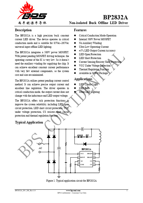
BP2832A
BP2832A_EN _DS_Rev.1.0
BPS Confidential – Customer Use Only
3
BP2832A
晶丰明源半导体
Symbol Supply Voltage Section VCC_CLAMP VCC_ON VCC_UVLO IST IOP VCC Clamp Voltage VCC Turn On Threshold VCC Turn off Threshold VCC Startup Current VCC Operating Current Threshold Voltage for Peak Current Limit Threshold Voltage for Peak Current Limit When Output Short Leading Edge Blanking Time for Current Sense Switch Off Delay Time Minimum OFF Time Maximum OFF Time Maximum On Time ROVP Pin Voltage Static Drain-source On-resistance Drain-Source Breakdown Voltage Power MOSFET Drain Leakage Current Thermal Regulation Temperature Output Short 1mA VCC Rising VCC Falling VCC= VCC-ON - 1V FOP=70KHz 16.8 13.8 9 120 100 180 150 V V V uA uA Parameter
3.2 x 2.8 mm PLCC2 SMD LED 商品说明书

Part Number Emitting Color Emitting MaterialLens-colorWavelength CIE127-2007*nm λPViewing Angle 2θ 1/2Luminous Intensity CIE127-2007* (I F =20mA) mcd *Luminous intensity value and wavelength are in accordance with CIE127-2007 standards.A Relative Humidity between 40% and 60% is recommended inESD-protected work areas to reduce static build up during assembly process (Reference JEDEC/JESD625-A and JEDEC/J-STD-033)Features● Ideal for indication light on hand held products ● Long life and robust package ● Standard Package: 2000pcs/ Reel ● MSL (Moisture Sensitivity Level): 3 ● Halogen-free ● RoHS compliantATTENTIONOBSERVE PRECAUTIONSFOR HANDLING ELECTROSTATIC DISCHARGE SENSITIVE DEVICESLED is recommended for reflow soldering and soldering profile is shown below.Forward Current Derating CurveThe device has a single mounting surface. The device must be mounted according to the specifications.Reel Dimension (Units : mm)Recommended Soldering Pattern (Units : mm; Tolerance: ± 0.1)Tape Specification (Units : mm)Remarks:If special sorting is required (e.g. binning based on forward voltage, Luminous intensity / luminous flux, or wavelength), the typical accuracy of the sorting process is as follows: 1. Wavelength: +/-1nm2. Luminous intensity / luminous flux: +/-15%3. Forward Voltage: +/-0.1VNote: Accuracy may depend on the sorting parameters.TERMS OF USE1. Data presented in this document reflect statistical figures and should be treated as technical reference only.2. Contents within this document are subject to improvement and enhancement changes without notice.3. The product(s) in this document are designed to be operated within the electrical and environmental specifications indicated on the datasheet. User accepts full risk and responsibility when operating the product(s) beyond their intended specifications.4. The product(s) described in this document are intended for electronic applications in which a person’s life is not reliant upon the LED. Please consult with a SunLED representative for special applications where the LED may have a direct impact on a person’s life.5. The contents within this document may not be altered without prior consent by SunLED.6. Additional technical notes are available at https:///TechnicalNotes.aspPACKING & LABEL SPECIFICATIONS。
853控制柜调试指导书
为099-100。
6.6.5. 再将载重量增加至额定载荷就可达到超载报警。
称重装置的插头端子对照表见下面表格。
6.7、舒适感调整一般情况下调整3319中的加速度、减速度及其jerk0-jerk3进行调整。
根据现场的实际情况而定,一般不调。
6.8、试外招和消防a用万用表量H4插键是否有短路,正常后插好,拨好地址码。
外召地址从21开始,一个地址一层,以此类推,按下按钮能呼到指定楼层,完毕。
b按下消防开关,电梯能返回指定楼层,且轿厢显示紧急退出,轿门一直打开,则正常。
以上结束后电梯上下反复运行几次,正常则调试完毕。
七、故障排除3.9编码器定位出厂时主机已经与控制柜进行配对试验,定位角度已经存在变频器中,如果发现主机运行异常或驱动器内参数与主机实际参数不符,则需要重新定位。
断电,将钢丝绳拨离曳引轮,短接SW-A1和BY-A1到AC110V,上电使接触器吸合,设置好驱动器参数和电机铭牌参数,将RUN SOURCE设成“0”,RUN ENABLE设成“0”。
用服务器插入SVT2,并按“M-3-3-2”并按“ENTER”键进行确认主机定位,注意:定位过程中主机将旋转(在此过程中要确认抱闸已经打开);等待服务器出现“Learning finished”表示定位完成;注意:如果电机相位更换,则需要进行重新定位,或更改成原来相位;3.10点动运行时,BY、SW不能正常吸合检查安全信号输入、输出(IO)信号是否正常,如不正常应根据原理图检查线路;如信号正常,请检查驱动器参数,参见驱动器参数表。
3.11点动运行时,接触器、抱闸继电器及抱闸正常打开,电机不转,电流很大“Drive Overload”。
可能是变频器到主机三相相序不对,应按照正确方法连接主机动力线,参见“2.6 动力线检查”。
3.12自学习运行到顶层后,电梯不能正常运行检查run enable值,应该设置成“1”,另外请检查井道信号是否正常。
3.13常见驱动器故障3.13.1驱动器“Over current”信息电流过大。
HK32C005 数据手册说明书
HK32C005数据手册版本:1.3发布日期:2023-08-15深圳市航顺芯片技术研发有限公司前言前言编写目的本文档介绍了HK32C005系列芯片的结构框图、存储器映射、外设接口、电气特性、引脚封装等,旨在帮助用户快速了解该系列芯片的特点及功能。
读者对象本文适用于以下读者:•开发工程师•芯片测试工程师•芯片选型工程师版本说明本文档对应的产品系列为HK32C005系列芯片。
修订记录目录1 简介 (1)2 产品概述 (2)2.1 产品特性 (3)2.2 器件一览表 (4)3 功能介绍 (6)3.1 结构框图 (6)3.2 存储器映射 (7)3.3 存储器 (7)3.3.1 Flash (7)3.3.2 内置SRAM (7)3.4 CRC计算单元 (7)3.5 供电方案 (8)3.6 电源监控器 (8)3.7 复位 (8)3.7.1 系统复位 (8)3.7.2 电源复位 (9)3.7.3 备份域复位 (9)3.8 时钟和时钟树 (9)3.9 SYSCFG (10)3.10 GPIO (10)3.11 Boot模式 (10)3.12 低功耗模式 (10)3.13 中断与事件 (10)3.13.1 NVIC (10)3.13.2 EXTI (11)3.14 独立看门狗(IWDG) (11)3.15 窗口看门狗(WWDG) (11)3.16 定时器 (11)3.16.1 高级定时器 (12)3.16.2 通用定时器 (12)3.17 DMA (13)3.18 ADC (13)3.18.1 内部参考电压 (13)3.19 温度传感器 (13)3.20 红外遥控接口(IRTIM) (13)3.21 I2C总线 (14)3.22 通用异步收发器(UART) (14)3.23 串行外设接口(SPI/I2S) (14)3.24 RTC (15)3.25 DVSQ计算单元 (15)3.26 96位UID (16)3.27 调试接口 (16)4 电气性能指标 (17)4.1 最大绝对额定值 (17)4.1.1 极限电压特性 (17)4.1.2 极限电流特性 (17)4.1.3 极限温度特性 (17)4.2 工作参数 (18)4.2.1 推荐工作条件 (18)4.2.2 低压检测 (18)4.2.3 上/下电复位特性 (18)4.2.4 内部参考电压 (18)4.2.5 工作电流特性 (19)4.2.6 外部高速(HSE)时钟特性 (20)4.2.7 内部高速(HSI)时钟特性 (20)4.2.8 内部低速(LSI)时钟特性 (21)4.2.9 PLL特性 (21)4.2.10 Flash存储器特性 (21)4.2.11 IO输入引脚特性 (21)4.2.14 TIM计数器特性 (22)4.2.15 ADC特性 (22)4.2.16 温度传感器特性 (24)5 典型电路 (26)5.1 电源供电 (26)6 引脚定义 (27)6.1 LQFP32封装 (27)6.2 LQFP32封装的引脚定义 (27)6.3 引脚复用(AF)功能表 (32)7 封装参数 (33)7.1 LQFP32封装 (33)7.2 LQFP32丝印 (34)8 订货信息 (35)8.1 订货代码 (35)8.2 订货包装 (35)9 缩略语与术语 (36)9.1 缩略语 (36)9.2 术语 (36)10 重要提示 (37)1简介本文档为HK32C005系列芯片的数据手册。
iSeries 控制器 CNi32 说明书
CNI3252-DC CNI3243CNI3253CNI3233CNI3233-C24-DC CNI32449-segment LEDThe OMEGA TM CNi32 is the iSeries controller in the extremely compact and increasingly popular 1⁄32 DIN size (22.5 x 45 mm cutout). The CNi32 is the most sophisticated and accurate instrument available in the small 1⁄32 DIN package, yet is still easy to configure.The CNi32 handles more thermocouple, RTD, process voltage and current inputs than any other 1⁄32 DIN controller.The CNi32 is the first 1⁄32 DIN controller with built‑in excitation for transmitters or other devices, 24 Vdc @ 25 mA.The CNiS32 has built‑in excitation for bridge transducers, 5 Vdc @ *********************communications options areinstalled, external excitation may be used and ratiometric operation maintained by connecting the external excitation to the sense leads. Both 4‑ or 6‑wire bridge configurations are supported for internal or external excitation.Non‑ratiometric operation is supported for voltage and current transducersand is also valuable in measuring offset and millivolt output of bridge devices during manufacturing and calibration. This model also features 10‑point linearization which allows the user to linearize the signal input from extremely nonlinear transducers of all kinds.The CNi32 introduces a number of unique features not yet found on any other 1⁄32 DIN instrument. The CNi32 is the first 1⁄32 DIN controller with a totally programmable display that can change color between GREEN, AMBER, and RED at any setpoint or alarm point.The unique 9‑segment LED characters greatly improves alphanumeric representations.The CNi32 is the first 1⁄32 DINcontroller offering 2 SPDT Form C relays, instead of the single throw relays on typical 1⁄32 DIN controllers.The CNi32 is the first to offerboth RS232 and RS422/485 serial communications in 1 instrument (C24 option). The ASCII protocol is selectable from the menu.U H igh Accuracy: ±0.03% Reading, 0.5°C (±0.9°F)U T otally Programmable Color Displays U U ser-Friendly,Simple to Configure U F ree Software U F ull AutotunePID ControlU U niversal Inputs: Thermocouple RTD, Process Voltage/ Current, Strain U R S232 and RS485Serial Communications (Optional)U B uilt-in Excitation U T emperature Stability ±0.04°C/°C RTD and ±0.05°C/°C TC @ 25°C (77°F)U N EMA 4 (IP65) Front Bezel U 2 Control or Alarm Outputs Optional: DC Pulse, Solid State Relays, Mechanical Relays, Analog Voltage and Current U F ront Removable and Plug ConnectorsCNi3233, smaller than actual size.CNi32 Series1⁄32 DIN Temperature,Process and Strain PID ControllersOrdering Examples: CNi3222-C24, 1⁄32 DIN PID controller with 2 solid-state relays for PID control and serial communications, both RS232 and RS485.CNiS322-AL, 1⁄32 DIN strain/process controller, limit alarm version with SSR output.DPi32-B-COVER front panel button cover supplied with eachunit, standard.CNi3233, shown smaller than actual size.CNi3244, shown smaller than actual size.2 “-AL ” option not available on models with analog (option 5) output.3 “-SM ” option not available on CNiS strain/process input models.Universal Temperature and Process Input (DPi/CNi Models) Accuracy: ±0.5°C temp; 0.03% rdg Resolution: 1°/0.1°; 10 µV process Temperature Stability:RTD: 0.04°C/°CTC @ 25°C (77°F): 0.05°C/°CCold Junction CompensationProcess: 50 ppm/°CNMRR: 60 dBCMRR: 120 dBA/D Conversion: Dual slope Reading Rate: 3 samples/sDigital Filter: Programmable Display: 4‑digit 9‑segment LED 10.2 mm (0.40"); i32, i16, i16D, i8DV 21 mm (0.83"); i8 10.2 mm (0.40") and 21 mm (0.83"); i8DH RED,GREEN, and AMBER programmable colorsfor process variable, setpoint and temperature unitsInput Types: Thermocouple, RTD, analog voltage, analog current Thermocouple Lead Resistance:100 Ω maxThermocouple Types (ITS 90):J, K, T, E, R, S, B, C, N, L (J DIN)RTD Input (ITS 68): 100/500/1000 ΩPt sensor, 2‑, 3‑ or 4‑wire; 0.00385 or 0.00392 curveVoltage Input: 0 to 100 mV, 0 to 1V, 0 to 10 VdcInput Impedance: 10 MΩ for 100 mV 1 MΩ for 1 or 10 VdcCurrent Input: 0 to 20 mA (5 Ω load) Configuration: Single‑ended Polarity: UnipolarStep Response: 0.7 sec for 99.9% Decimal Selection: Temperature: None, 0.1 Process: None, 0.1, 0.01 or 0.001 Setpoint Adjustment:‑1999 to 9999 countsSpan Adjustment:0.001 to 9999 countsOffset Adjustment: ‑1999 to 9999 Excitation (Not Included with Communication): 24 Vdc @ 25 mA (not available for low‑power option) Universal Strain and Process Input (DPiS/CNiS Models) Accuracy: 0.03% reading Resolution: 10/1µVTemperature Stability: 50 ppm/°C NMRR: 60 dBCMRR: 120 dBA/D Conversion: Dual slope Reading Rate: 3 samples/sDigital Filter: ProgrammableInput Types: Analog voltage and current Voltage Input: 0 to 100 mVdc,‑100 mVdc to 1 Vdc, 0 to 10 Vdc Input Impedance: 10 MΩ for 100 mV;1 MΩ for 1V or 10 VdcCurrent Input: 0 to 20 mA (5 Ω load) Linearization Points: Up to 10 Configuration: Single‑ended Polarity: UnipolarStep Response: 0.7 sec for 99.9% Decimal Selection: None, 0.1, 0.01or 0.001Setpoint Adjustment:‑1999 to 9999 countsSpan Adjustment: 0.001 to 9999 counts Offset Adjustment: ‑1999 to 9999 Excitation (Optional In Place Of Communication): 5 Vdc @ 40 mA;10 Vdc @ 60 mAControlAction: Reverse (heat) or direct (cool) Modes: Time and amplitude proportional control; selectable manual or auto PID, proportional, proportional with integral, proportional with derivative and anti‑reset Windup, and on/offRate: 0 to 399.9 sReset: 0 to 3999 sCycle Time: 1 to 199 s; set to 0 for on/off Gain: 0.5 to 100% of span; setpoints 1 or 2 Damping: 0000 to 0008Soak: 00.00 to 99.59 (HH:MM), or OFF Ramp to Setpoint:00.00 to 99.59 (HH:MM), or OFFAuto Tune: Operator initiated fromfront panelControl Output 1 and 2Relay: 250 Vac or 30 Vdc @ 3 A (resistive load); configurable for on/off, PID and ramp and soakOutput 1: SPDT, can be configured as alarm 1 outputOutput 2: SPDT, can be configured as alarm 2 outputSSR: ******************.5A (resistive load); continuousDC Pulse: Non‑isolated; 10 Vdc @ 20 mA Analog Output (Output 1 Only):Non‑isolated, proportional 0 to 10 Vdc or 0 to 20 mA; 500 Ω maxOutput 3 Retransmission:Isolated Analog Voltage and Current Current: 10 V max @ 20 mA output Voltage: 20 mA max for 0 to 10 V output Network and Communications Ethernet: Standards complianceIEEE 802.3 10 Base‑TSupported Protocols:TCP/IP, ARP, HTTPGETRS232/RS422/RS485: Selectable from menu; both ASCII and MODBUS protocol selectable from menu; programmable 300 to 19.2 Kb; complete programmable setup capability; program to transmit current display, alarm status, min/max, actual measured input value and statusCommon Specifications(All i/8, i/16, i/32 DIN)RS485: Addressable from 0 to 199Connection: Screw terminalsAlarm 1 and 2 (Programmable)Type: Same as output 1 and 2Operation: High/low, above/below,band, latch/unlatch, normally open/normally closed and process/deviation;front panel configurationsAnalog Output (Programmable):Non‑isolated, retransmission 0 to 10 Vdcor 0 to 20 mA, 500 Ω max (output 1 only);accuracy is ± 1% of FS when followingconditions are satisfied: input is not scaledbelow 1% of input FS, analog output is notscaled below 3% of output FSGeneralPower: 90 to 240 Vac ±10%, 50 to 400Hz*, 110 to 300 Vdc, equivalent voltageLow Voltage Power Option: 24 Vac**,12 to 36 Vdc for DPi/CNi/DPiS/CNiS;20 to 36 Vdc for dual display, ethernetand isolated analog output from qualifiedsafety approved sourceIsolationPower to Input/Output: 2300 Vacper 1 minute testFor Low Voltage Power Option:1500 Vac per 1 minute testPower to Relay/SSR Output:2300 Vac per 1 minute testRelay/SSR to Relay/SSR Output:2300 Vac per 1 minute testRS232/485 to Input/Output:500 Vac per 1 minute testEnvironmental Conditions:All Models: 0 to 55°C (32 to 131°F)90% RH non‑condensingDual Display Models:0 to 50°C (32 to 122°F), 90% RHnon‑condensing (for UL only)Protection:D Pi/CNi/DPiS/CNiS32,16,16D, 8C:NEMA 4X/Type 4 (IP65) front bezelDPi/CNi/DPiS/CNiS8, 8DH, 8DV:NEMA 1/Type 1 front bezelApprovals: UL, C‑UL, CE per2014/35/EU, FM (temperatureunits only)Dimensionsi/8 Series: 48 H x 96 W x 127 mm D(1.89 x 3.78 x 5")i/16 Series: 48 H x 48 W x 127 mm D(1.89 x 1.89 x 5")i/32 Series: 25.4 H x 48 W x 127 mm D(1.0 x 1.89 x 5")Panel Cutouti/8 Series: 45 H x 92 mm W(1.772 x 3.622"), 1⁄8 DINi/16 Series: 45 mm (1.772") square,1⁄16 DINi/32 Series: 22.5 H x 45 mm W(0.886 x 1.772"), 1⁄32 DINWeighti/8 Series: 295 g (0.65 lb)i/16 Series: 159 g (0.35 lb)i/32 Series: 127 g (0.28 lb)* No CE compliance above 60 Hz.** Units can be powered safely with 24 Vacpower, but no certification for CE/UL are claimed.CNI3252-DC CNI3243CNI3253CNI3233CNI3233-C24-DC CNI3244。
- 1、下载文档前请自行甄别文档内容的完整性,平台不提供额外的编辑、内容补充、找答案等附加服务。
- 2、"仅部分预览"的文档,不可在线预览部分如存在完整性等问题,可反馈申请退款(可完整预览的文档不适用该条件!)。
- 3、如文档侵犯您的权益,请联系客服反馈,我们会尽快为您处理(人工客服工作时间:9:00-18:30)。
MC5328 用户手册V0.1
非隔离降压型LED驱动芯片
2014/3/21
上海晟矽微电子股份有限公司
Shanghai SinoMCU Microelectronics Co., Ltd.
概述
MC5328 是一款带有源功率因数校正的高精度降压
型LED 恒流控制芯片,适用于85Vac-265Vac 全范围输入电压的非隔离降压式LED 恒流电源。
MC5328 集成有源功率因数校正电路,可以实现很高的功率因数和很低的总谐波失真。
由于工作在电感电流临界连续模式,功率MOS 管处于零电流开通状态,开关损耗得以减小,同时电感的利用率也较高。
MC5328 内部集成600V 功率MOSFET,只需要很少的
外围器件,即可实现优异的恒流特性.
MC5328对电感电流进行全周期采样,可实现高精度输出恒流控制,并达到优异的线电压调整率和负载调整率。
MC5328 具有多重保护功能以加强系统可靠性,包括LED 开路保护、LED 短路保护、芯片供电欠压保护、电流采样电阻开路保护和逐周期限流等。
所有的保护状态都具有自动重启功能。
另外,MC5328 具有过热调节功能,在驱动电源过热时减小输出电流,以提高系统的可靠性。
MC5328 采用SOP-8封装
典型应用特性
. 单级、有源功率因数校正,高PF 值,低THD . 内置600V 功率MOSFET
. ±3% LED 输出电流精度
. 优异的线电压调整率和负载调整率
. 电感电流临界连续模式
. 超低 (33uA) 启动电流
. 高达95%的系统效率
. 超低 (300uA) 工作电流
. LED 开路/短路保护
. 电流采样电阻开路保护
. 逐周期原边电流限流
. 芯片供电过压/欠压保护
. 自动重启功能
. 过热调节功能
图1 MC5328典型应用图
引脚图
极限参数
电气特性
内部框图
图3 芯片内部框图
功能说明
MC5328 是一款内部集成600V 功率MOSFET 的有源功率因数校正LED 恒流控制芯片,用于非隔离降压型电路,系统工作在电感电流临界连续模式, 可以实现很高的功率因数、很低的总谐波失真和高效率。
启动
在系统上电后,母线电压通过启动电阻给V DD 引脚的电容充电,当V DD 电压上升到启动阈值电压后, 芯片内部控制电路开始工作,COMP 电压被快速上拉到1.5V 。
然后MC5328 开始输出脉冲信号,系统刚开始工作在10kHz 开关频率,COMP 电压从1.5V 开始逐渐上升,电感峰值电流随之上升,从而实现输出LED 电流的软启动,有效防止输出电流过冲。
当输出电压建立之后,V DD 电压由输出电压通过二极管供电,从而降低系统功耗。
采样电阻与恒流控制
MC5328工作于原边反馈模式,无需次级反馈电路,
即可实现高精度输出恒流控制。
LED 输出电流计算方法:
其中, V REF 是内部基准电压 ;R ISEN 是电流采样电阻的值。
过零检测
MC5328 通过ZCD 来检测输出电流过零的状态,ZCD 的下降阈值电压设置在0.2V ,迟滞电压为0.15V 。
ZCD 引脚也可以用来探测输出过压保护(OVP ),阈值为1.6V 。
ZCD 的上下分压电阻比例可以设置为:
其中, R ZCDL是反馈网络的下分压电阻;R ZCDH是反馈网络的上分压电阻;V OVP是输出电压过压保护设定点;推荐ZCD下分电阻设置在3K –10K左右。
过温调节
MC5328 具有过热调节功能,在驱动电源过热时逐渐减小输出电流,从而控制输出功率和温升,使电源温度保持在设定值,以提高系统的可靠性。
芯片内部设定过热调节温度点为150℃。
保护功能
MC5328 内置多重保护功能,保证了系统可靠性。
当LED 开路时,输出电压逐渐上升,ZCD引脚可以在功率管关断时检测到输出电压,当输出电压高到使ZCD电压高于1.6V,则触发保护逻辑并停止开关工作。
当LED 短路时,系统工作在10kHz 低频。
由于输出电压很低,无法通过二极管给V DD供电,所以V DD 电压逐渐下降直到欠压保护阈值。
系统进入保护状态后,V DD电压开始下降,当V DD到达欠压保护阈值时,系统将重启。
同时系统不断的检测系统状态,如果故障解除,系统会重新开始正常工作。
当输出短路或者变压器饱和时,ISEN 峰值电压将会比较高。
当ISEN 电压上升到内部限制值(1V)时,该开关周期马上停止。
此逐周期限流功能可以保护功率MOS 管、变压器和输出续流二极管。
PCB设计
在设计MC5328 PCB时,需要遵循以下指南:
旁路电容
V DD的旁路电容需要紧靠芯片V DD和GND 引脚。
地线
电流采样电阻的功率地线尽可能粗,且要离芯片的地(Pin2)尽量近,以保证电流采样的准确性,否则可能会影响输出电流的调整率。
另外,信号地需要单独连接到芯片的地引脚。
功率环路的面积
减小大电流环路的面积,如变压器主级、功率管及吸收网络的环路面积,以及变压器次级、次级二极管、输出电容的环路面积,以减小EMI 辐射。
ZCD 引脚
接到ZCD的分压电阻必须靠近ZCD 引脚,且节点要远离变压器的动点,否则系统噪声容易误触发ZCD OVP 保护功能,在R ZCDL并联旁路电容可以提高抗干扰能力。
DRAIN 引脚
增加DRAIN引脚的铺铜面积以提高芯片散热。
封装形式
SOP8 package outline dimensions。
