TI电源管理指南3
ti电源方案
TI电源方案概述TI(Texas Instruments)是一家全球领先的半导体解决方案供应商,在电源管理领域有着丰富的经验和广泛的产品线。
TI电源方案以其高效性、可靠性和创新性而闻名,广泛应用于各种电子设备和系统中。
本文将介绍TI电源方案的特点、应用领域和相关产品系列,并对其优势做出评估。
特点TI电源方案具有以下几个突出的特点:1. 高效性TI电源方案采用了先进的功率管理技术,能够提供高效的转换效率。
TI的产品具有低静态功耗、快速响应和高效的功率转换能力,为电子设备提供了更长的续航时间和更高的性能。
2. 可靠性TI电源方案经过严格的设计和测试,以确保其长期稳定和可靠性。
TI的产品在工作温度范围、负载容忍度和短路保护等方面表现出色,可以满足各种苛刻的工作环境和条件。
3. 创新性TI电源方案不断引入创新的设计和技术,以满足新兴的应用需求和市场趋势。
TI的研发团队致力于推动电源管理技术的发展,提供更高效、更便捷和更多样化的解决方案,支持客户的创新和竞争力。
应用领域TI电源方案广泛应用于各种电子设备和系统中,包括但不限于:1. 通信设备TI电源方案可为各种通信设备提供高效的电源管理。
无论是移动通信基站、无线路由器还是手机和平板电脑,TI的产品都能够满足其对功率转换、电池管理和系统保护的需求。
2. 工业自动化在工业自动化领域,TI电源方案可以提供稳定可靠的电源供应。
无论是PLC、工控机还是传感器和执行器等设备,TI的产品都能够满足其对高效能源转换和电源可靠性的要求。
3. 汽车电子汽车电子领域对电源管理的需求非常严苛,TI电源方案可以满足其对高温环境下工作、抗干扰和快速响应的要求。
无论是汽车电池管理系统还是车载娱乐和驾驶辅助设备,TI的产品都能够提供稳定和可靠的电源供应。
相关产品系列TI电源方案涵盖了多个产品系列,以满足不同应用需求。
以下是几个主要的产品系列:1. Switching RegulatorTI的Switching Regulator系列产品提供了高效能源转换和稳定的电源供应。
满足处理器内核电压要求的电源管理

5A 0
+ 5
T2 F PTH .
PTH0 4T2 F 60
PTHO8 60 T2 F
P THO 4T2 0F 3
P THO 8T2 OF 3
PTH04 40F T2
PTH0 T24 8 0F
P TH0 4T2 0F 2
PTH0 8T2 0F 2
点 电源 模 块 产 品 。表 2 示 为 超 高 速 瞬 所
态 响 应 模 块 产 品 。 表 1 表 2 示 的 新 和 所 量
怡
窿
型 T 2系 列 插 入 式 电 源模 块 具 有 一 种 称 为 T r o a s 申请 专 利 中)的 新 型 特 u b Tr n (
性 。 T r o rn u b T a s技 术 可 以 帮 助 设 计 人 员
表2超高速 瞬态 响应 T 2非 隔离式 负载点 电源模块 产 品选择 列表
V N V I( )
+3. 3
描述
T2 F PTH .
3 A
PTHO4 6O T2 F
6 A
P TH0 4T2 0F 3
1A 0
PTH0 T24 4 0F
1A 6
PTH0 4T2 OF 2
3A O
少 两 个 电压 。 一 个 电压 用 于 满 足 处 理 器 内核 电压要 求 ,即V 。 而 其 它 电压 则
电压容 差 、噪声 以及 瞬态
产 品 说 明 书 中规 定 的 电 压 容 差 包
用 于 满 足 输 入 一 出 电压 要 求 , 即 V。 输 。 内 核 电压要 求介 于09 . V~1 3 . V之 间 ,且 通 常 取 决 于 具 体 的 处 理 器 性 能 标 准 。 最 新 的 内 核 电 源 电 压 容 差 通 常
TI经典资料 精选

【TI】经典不过时一直以来,TI的资料都大受欢迎,也都是很实用的资料,所以今日,小编就为大家整理一番。
请带好眼镜,清楚下大脑缓存,赶紧开始学习啦。
话说资料都是贵精不贵多,所以小编这次精选了17本资料为大家分享,都是好评超高的。
1.模拟电路葵花宝典: 运算放大器稳定性分析(TI)(强烈推荐)作者:Tim Green,TI公司Burr-Brown产品战略发展经理全书一共15部分,详细分析了运放的稳定性原理,是一本不可多得的好书2.绝对好东西,TI工程师关于运放噪声分析+滤波+测量作者:德州仪器公司高级应用工程师Art Kay我们可将噪声定义为电子系统中任何不需要的信号。
噪声会导致音频信号质量下降以及精确测量方面的错误。
板级与系统级电子设计工程师希望能确定其设计方案在最差条件下的噪声到底有多大,并找到降低噪声的方法以及准确确认其设计方案可行性的测量技术。
噪声包括固有噪声及外部噪声,这两种基本类型的噪声均会影响电子电路的性能。
外部噪声来自外部噪声源,典型例子包括数字交换、60Hz 噪声以及电源交换等。
固有噪声由电路元件本身生成,最常见的例子包括宽带噪声、热噪声以及闪烁噪声等。
本系列文章将介绍如何通过计算来预测电路的固有噪声大小,如何采用SPICE模拟技术,以及噪声测量技术等。
3.TI 电源开关设计秘笈30 例电源设计一直是工程师面对的一个难题,随着全球节能环保意识的提升,设计简捷、高效、轻巧的绿色电源成为工程师的首要任务,为了帮助工程师解决这方面的难题,现在特别隆重推出大量实用资料供工程师朋友下载,目前推出的一本电子书叫做《电源开关设计秘笈30 例》,对电源开关设计技巧做出了详细的说明,相信一定对工程师朋友们有很大帮助。
4.TI通用质量指南本通用质量指南(GQG) 适用于TI提供的有关材料、产品、服务、制造工艺、测试、控制、处置、贮存和运输措施的质量保证,以及TI所采用和/或应用的旨在确保TI部件与已公布和/或特别指明的规格相符合的管理流程。
TI正负双电源芯片TPS65130EVM-063评估板用户指南
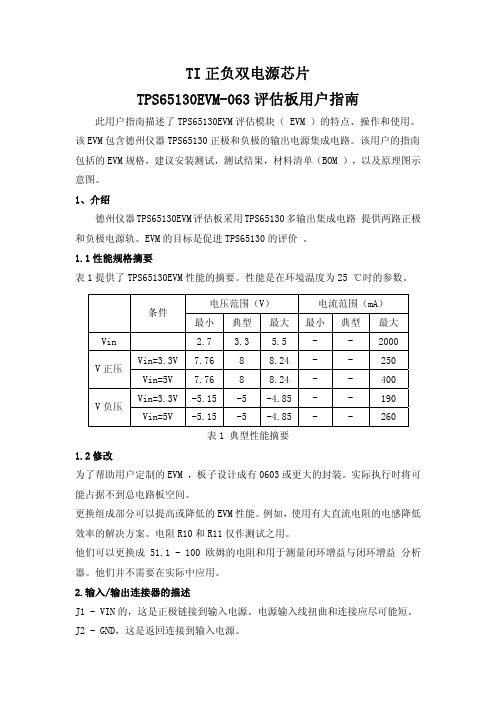
最小 典型 最大 最小 典型 最大
Vin
2.7 3.3 5.5
-6 8 8.24 V 正压
Vin=5V 7.76 8 8.24 -
-
250
-
400
Vin=3.3V -5.15 -5 -4.85 V 负压
Vin=5V -5.15 -5 -4.85 -
-
190
-
260
表 1 典型性能摘要
器。他们并不需要在实际中应用。
2.输入/输出连接器的描述
J1 - VIN 的,这是正极链接到输入电源。电源输入线扭曲和连接应尽可能短。
J2 - GND,这是返回连接到输入电源。
J3 - VPOS 这是设备的正极输出。 J4 - GND 这是返回连接的负载正极转换装置。 J5 - VNEG 这是设备的负极输出。 J6 - GND 这是返回连接的负载负极转换装置。 JP1 - ENP ,这是使能引脚的正极转换器( VPOS ) 。放置跳线连接引脚 2-3 JP1 短接使能引脚与 GND ,从而禁用该设备。放置跳线连接引脚 1-2 的 JP1 连接 ENABLE 引脚至 VIN ,使该设备工作。 JP2 - PSP,这是控制引脚为节电模式的正极转换。放置跳线连接引脚 2-3 JP2 短接引脚与 GND ,从而禁用节电模式。放置跳线连接引脚 1-2 的 JP2 连接引脚 至第六,从而使节电模式。 JP3 - ENN 这是 ENABLE 引脚的负极转换器( VNEG ) 。放置跳线连接引脚 2-3 JP3 短接 ENABLE 引脚与 GND ,从而禁用该设备。放置跳线连接引脚 1-2 的 JP3 连接 ENABLE 引脚至 VIN ,使该设备。 JP4 - PSN 这是控制引脚为节电模式的负极转换。配售跳投 整个引脚 2-3 JP4 短接引脚与 GND ,从而禁用节电模式。配售跳投 在引脚 1-2 的 JP4 连接引脚至 Vi,从而使节电模式。 2.1 测试安装 绝对最大输入电压为 6V, TPS65130 设计的最大输入工作电压为 5.5V,连接的 电源设置输出电压为 2.7 V 和 5.5 V 之间和电流限制在 3A 以上。短引脚 1 -2 的跳线 JP1 和 JP2 ,使能这两个导轨。 2.2 测试结果 以下 EVM 板的使用效率结果:
TI电源管理选择指南
PWM Controllers
(Page 16)
Backplane
MOSFET Drivers (Page 22)
Hot Swap and
Power-over-Ethernet (Page 51)
Non-Isolated Plug-In Modules
POLA™
(Page 25)
+
–
48-V
48-V or 24-V DC Input
Audio Supply
Noise-Sensitive RF Circuitry
Step-Up DC/DC Converters (Page 34)
Inductorless DC/DC Regulators
(Charge Pumps) (Page 39)
Battery Management
DC Inputs
Secondary Side Control (Page 16, 22)
PWM UC3849 UCC3839
Drivers TPS2811-15 TPS28225 TPS28226 TPS2829-29 UCC27423/4/5 UCC37321/2 UCC37323/4/5 UCD7100 UCD7201
USB
Battery Charge Management
(Page 46)
Lithium-Ion Protection and Authentication
for Batteries (Pages 50, 51)
Rechargeable Battery
Battery Fuel Gauges
(Page 48)
Isolated Plug-In Modules (Page 25)
TI产品中文版说明书
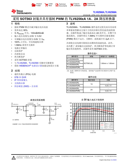
Load (A)E f f i c i e n c y (%)0.00.51.0 1.52.06065707580859095100D008V INV OUTL1TLV62569AProduct Folder Order Now Technical Documents Tools &SoftwareSupport &CommunityTLV62568A ,TLV62569AZHCSI23B –APRIL 2018–REVISED MARCH 2020采用SOT563封装并具有强制PWM 的TLV6256xA 1A 、2A 降压转换器1特性•强制PWM 模式可减少输出电压纹波•效率高达95%•低R DS(ON)开关:100m Ω/60m Ω•输入电压范围为2.5V 至5.5V •可调输出电压范围为0.6V 至V IN •100%占空比,可实现超低压降• 1.5MHz 典型开关频率•电源正常输出•过流保护•内部软启动•热关断保护•采用SOT563封装•与TLV62568、TLV62569引脚对引脚兼容•借助WEBENCH ®电源设计器创建定制设计方案2应用•通用负载点(POL)电源•STB 和DVR •IP 网络摄像头•无线路由器•固态硬盘(SSD)–企业级3说明TLV62568A 、TLV62569A 器件是经过优化而具有高效率和紧凑型解决方案尺寸的同步降压型直流/直流转换器。
该器件集成了输出电流高达2A 的开关。
在整个负载范围内,该器件将以1.5MHz 开关频率在脉宽调制(PWM)模式下运行。
关断时,流耗减少至2μA 以下。
内部软启动电路可限制启动期间的浪涌电流。
此外,还内置了诸如输出过流保护、热关断保护和电源正常输出等其他特性。
该器件采用SOT563封装。
器件信息(1)器件型号封装封装尺寸(标称值)TLV62568ADRL SOT563(6)1.60mm x 1.60mmTLV62568APDRL TLV62569ADRL TLV62569APDRL(1)如需了解所有可用封装,请参阅产品说明书末尾的可订购产品附录。
TI电源管理芯片指南

非隔离式开关 DC/DC 稳压器 . . . . . . . . . . . . . . . . . . . . . . . . . . . . 31
DC/DC 控制器 (外接开关) . . . . . . . . . . . . . . . . . . . . . . . . . . . . . . . . . . . . . . . . . . . . . . . . . . . 31 DC/DC 转换器 (集成开关) . . . . . . . . . . . . . . . . . . . . . . . . . . . . . . . . . . . . . . . . . . . . . . . . . . . 33 无电感器 DC/DC 稳压器 (充电泵) . . . . . . . . . . . . . . . . . . . . . . . . . . . . . . . . . . . . . . . . . . . . . 38
插入式电源模块 . . . . . . . . . . . . . . . . . . . . . . . . . . . . . . . . . . . . . . 24 线性稳压器 . . . . . . . . . . . . . . . . . . . . . . . . . . . . . . . . . . . . . . . . . . . 27t 指南 Guide
汽车 通信 计算 消费类电子 高可靠性 工业
/power
2010 年
2
电源管理指南
目录
典型电源应用 . . . . . . . . . . . . . . . . . . . . . . . . . . . . . . . . . . . . . . . . . . 3
TI针对电源管理推出的impedance track技术

TI针对电源管理推出Impedance Track™技术(华强电子世界网讯)日前,德州仪器 (TI) 凭借其在电池管理方面雄厚的研发实力宣布推出一款功能独特的“电量监测计”技术,能够在电池整个寿命周期内以高达 99% 的精确度计算锂电池组的剩余电量。
新型Impedance Track™ 技术使便携式医疗设备、工业设备以及笔记本的设计人员和用户能够延长电池使用寿命,并始终能了解电池内剩余的可用能量。
TI 的创新型阻抗跟踪技术可精确监测阻抗改变或由电池老化、温度以及循环模式造成的电阻,从而准确预计双节池组、三节电池组和四节电池组的运行时间。
该技术集成在TI 基于闪存的 bq20z8x 电量监测计芯片组中,在电池组处于静止状态时,通过在相应的温度下关联电池组的空载电压和充电状态可以分析出准确的电荷状态。
该技术能够从静态电压中明确得出准确的“起始和终止位置”,并从相应的容量差中得出总容量,从而消除了完全充电与放电的必要。
对于如心脏起搏器等特定应用或用于电信系统(从不完全放电)中的电池组而言,阻抗跟踪将确保我们始终能够实时获得准确的电量信息。
阻抗跟踪依靠动态建模算法得知电池随着老化、温度或使用产生了多少衰减,并关联电池电解槽中阳极/阴极的典型化学属性,而跟电池属于何种品牌无关。
事实上,阻抗跟踪允许在同一电池组中混合使用来自不同制造商的电池,这就实现了电源的灵活性与持续性。
目前许多电量监测计集成电路技术均依赖静态而不可靠的建模技术,要求创建大型数据库才能测量数百种可用电池参数的具体属性。
而即将获得专利的阻抗跟踪技术能够显著降低 OED 及 OEM 厂商所需的开发与实施设置时间,可保证获得正确的特性,因为我们再也不需要什么数据库了。
双芯片 bq20z8x 电量监测计通过系统管理总线 (SMBus) 接口向系统主机控制器报告电量信息。
诸如 TMS320C55x 数字信号处理器等主机控制器管理剩余电池电量的目的在于进一步延长系统的运行时间。
TI 各类电源方案图表,经验值,包含PWM,LLC,PFC等
Desktop and Server P/S LCD-TV and PDP-TV Hi-Power Adapters
Over Voltage & Open Loop Detection Protection 1.5A/ 2A Source/Sink
Input Voltage BrownOut Protection
Matterhorn Single Phase CCM,DCM, TM PFC w/ LL Management
Enhanced 8-pin CCM PFC Samples Today
2008
2009
2010
2011
2012
UCC28019A 8-Pin CCM (ACM) PFC Controller
EMI Filter
Price / Performance
UCD3040 80-pin Dig. Cont. UCD7201 4A Dual Digital Compatible Gate Driver UCD7100 4A Single Ended Digital Compatible Gate Driver UCC28070 2-phase CCM PFC UCC28060/1 2-phase TM PFC UCC28019 8-pin CCM PFC UCC28019A UCD3040
R1
RDM CDR
M 1
Cref 16 Vpk 15 IS1 14 CAO1 13 CAO2 12 IS2 11
T2 L2 D2
ቤተ መጻሕፍቲ ባይዱ
Css
6 SS 7 VAO 8 SENSE 9 VAC 10 RDS
Frequency dither
R2 RDS Cp2
非隔离开关DC-DC稳压器--TI 电源管理选择指南

DC/DCDC/DC控制器(外置开关)
TPS40200是灵活的非同步控制器,内置了200mA驱动器以用于P道沟FET。其电路工作电压高达52V,并带有特色的功耗节省功能,可在外部FET完全开启状态下关闭驱动电流。此电路工作是带有电压模式的反馈,并前馈至输入电压输入电压补偿以实现对输入电压变化的即时响应。
DC/DC控制器(集成开关)
TI的低功耗DC/DC转换器系列(TPS6XXXX)以及SWIFTTM(TPS54XXX)负载点步降DC/DC转换器可实现97%的峰值效率。同步整流不仅取代了所需的外部肖特基整流二极管,同时还使转换器效率的提升高达10% 。更高的效率意味着电池驱动应用中延长的运转时间,并降低了大电流应用中的功率损耗,也放宽了对散热设计的要求。因外部仅需电阻、电容及单个电感支持工作,集成的高侧及低侧开关FET就稳压器--TI 电源管理电源管理选择指南.pdf
TI电源管理指南7

TI电源管理指南7TI电源管理指南7第一部分:引言TI电源管理指南7是一本针对电源管理的综合手册,由TI公司编写而成。
本指南旨在帮助读者了解电源管理的基本概念和原则,并提供设计和应用方面的相关信息。
本文将对电源管理的关键概念和技术进行介绍,并探讨现代电源管理技术的最新发展。
第二部分:电源管理概述在本部分中,我们将讨论电源管理的基本概念和原则。
首先,我们将介绍电源管理的主要目标和需求,包括提高能源利用效率、增强系统稳定性和可靠性等。
然后,我们将探讨电源管理系统的基本组成部分,包括DC-DC转换器、LDO稳压器、电池充电器等。
最后,我们将介绍电源管理领域的主要挑战和机遇。
第三部分:关键技术本部分将介绍电源管理的关键技术,包括节能技术、功率因数校正技术、降压转换器设计等。
我们将详细介绍每个技术的原理和应用,并提供相关的设计建议和实例。
此外,我们还将讨论无线充电和高效能量传输等新兴技术,以及其在电源管理中的应用。
第四部分:现代电源管理的最新发展在本部分中,我们将介绍现代电源管理技术的最新发展,并探讨其在实际应用中的优势和挑战。
我们将讨论新型电源管理芯片和模块的特点和功能,并对其未来发展进行展望。
此外,我们还将介绍一些实际案例,包括电动汽车、太阳能电池等的应用,以展示电源管理技术的应用价值和前景。
第五部分:设计和应用指南在本部分中,我们将提供设计和应用方面的指南和建议。
我们将详细介绍电源管理系统的设计流程和关键参数选择,以及相关的测试和验证方法。
此外,我们还将提供一些常见问题的解决方案和设计实例,帮助读者解决实际应用中的挑战。
结论TI电源管理指南7是一本全面而详细的电源管理手册,涵盖了电源管理的关键概念、技术和最新发展。
本指南提供了设计和应用方面的指南和建议,帮助读者在实际应用中有效地应用电源管理技术。
阅读本指南将有助于读者提高对电源管理的理解和应用能力,从而推动电源管理技术的发展和创新。
惠普电源管理使用指南说明书

電源管理使用指南© Copyright 2007 Hewlett-Packard Development Company, L.P.Windows 是 Microsoft Corporation 在美國的註冊商標。
本文件包含的資訊可能有所變更,恕不另行通知。
HP 產品與服務的保固僅列於隨產品及服務隨附的明確保固聲明中。
本文件的任何部份都不可構成任何額外的保固。
HP 不負責本文件在技術上或編輯上的錯誤或疏失。
第一版:2007 年 7 月文件編號: 446624-AB1產品聲明本使用指南會說明大部份機型一般所使用的功能。
有些功能可能無法在您的電腦上使用。
iiiiv產品聲明目錄1 電源控制項與指示燈位置2 設定電源選項使用省電狀態 (3)啟動和結束睡眠 (3)啟動和結束休眠 (4)電池計量器的使用方法 (5)使用電源計劃 (6)檢視目前的電源計劃 (6)選擇不同的電源計劃 (6)自訂電源計劃 (6)設定喚醒時使用密碼保護 (7)3 使用電池電源尋找「說明及支援」中的電池資訊 (9)顯示剩餘的電池電力 (10)裝入或取出電池 (11)電池充電 (12)管理低電池電力 (13)識別低電池電力 (13)解決低電池電力的方法 (14)可以使用外部電源時,解決低電池電力的方法 (14)當可以使用已充電的電池時,解決低電池電力的方法 (14)當沒有電源可以使用時,解決低電池電力的方法 (14)當電腦無法結束休眠時,解決低電池電力的方法 (14)校正電池 (15)步驟 1:將電池完全充飽 (15)步驟 2:停用休眠和睡眠 (15)步驟 3:釋放電池的電力 (16)步驟 4:將電池完全充飽電 (17)步驟 5:重新啟用休眠和睡眠 (17)節省電池電力 (18)存放電池 (19)用過電池處置方式 (20)4 使用外部的 AC 電源連接 AC 轉接器 (22)v5 電腦關機索引 (24)vi1電源控制項與指示燈位置下列圖例和表格識別及說明電源控制和指示燈位置。
TI推出了5款电源管理芯片可高效提取和管理微瓦至毫瓦级电源
TI推出了5款电源管理芯⽚可⾼效提取和管理微⽡⾄毫⽡级电源现在的⼀些消费类、⼯业类、医疗类及汽车类的产品中,容量更⼤的电池并不适⽤,甚⾄没有空间存放电池,更别说对电池进⾏快速充电。
例如,⼀些可穿戴设备、远程监控设备和传感器⽹络等,这些应⽤难以持续供电,只能从周围环境或传感器获取能量。
可以说,它们其实没有⼈为地供电,是⼀种⽆电池⼯作。
因此,以微电源为输⼊能源的解决⽅案将有很⼤的市场空间,⽽如何采集这些五花⼋门的微⼩能量并加以应⽤成为新兴课题。
近⽇,德州仪器推出了5款电源管理芯⽚bq25570、bq25505、TPS62740、TPS62737与TPS62736,能⾼效提取和管理从光源、热源或机械能源采集的微⽡⾄毫⽡级电源,在开启下⼀代能量采集的竞争中先发制⼈。
TI电池管理市场及应⽤经理⽂司华博⼠向记者详细介绍了这⼏款芯⽚的优势。
⽂博⼠说:“我们经常需要系统级的电源⽅案,但最⼤的难题是,什么样的电源才能适⽤于应⽤场景,电源⽆疑是很重要的,在任何情况下有⾯向该应⽤的最低功耗解决⽅案。
TI提供的全套技术⽅案,包括电源管理和⾼精度的模拟IC,这是我们最⼤的专长;另外,我们有⾮常低功耗的微控制器,低功耗的⽆线连接,包括Wi-Fi、ZigBee、蓝⽛以及1个Sub-1GHz集成的芯⽚。
我们希望在能量采集概念范畴下,能从光、热量、振动、RF上去获取能量,为控制器进⾏供电。
但⼀个很⼤的挑战摆在⾯前,⼀般的DC/DC转换器,如⽤在⼿持设备上的单节锂电池,输⼊电流在1A左右,很少在50 mA以下,输⼊电压在1.8 V以下也⽐较少,⼀般都是3 V或2.5 V以上。
⽽太阳能(10~10 000 uW/cm2)、热量(25~1000 uW/cm2)、振动(50~250 uW/cm2)、RF(0.01~0.1 uW/cm2)的能量采集,它们所提供的电压⾮常少,可能少于1 V,电流也是毫安级或微安级的。
因此,能量采集技术的要点即最⼤的挑战就是能够把这些输⼊微电源收集起来,这就需要去研究拓扑结构和更深层次的芯⽚设计。
TI 控制模式快速参考指南说明书

Control-mode quick reference guideOverviewTI is active in the development of leading-edge controlcircuits to help engineers address specific designchallenges. Since no control mode is optimal for everyapplication, various control modes for non-isolated step-down controllers and converters are referenced with theiradvantages and how to learn more about each mode.The TI portfolio contains 15 types of control architecturesfor non-isolated TPS- and LM-series switching DC/DCconverters and controllers.Voltage modeInternally-compensatedadvanced currentmode (ACM)Direct connection tothe output capacitor(D-CAP™)Voltage mode with voltage feed-forward Hysteretic controlmodeD-CAP+™controlmodePeak current mode Constant on-time D-CAP2™ controlmodeAverage currentmodeConstant on-timewith emulated ripplemodeD-CAP3™ controlmodeEmulated currentmodeDCS-Control™:Direct control withseamless transitioninto power-savemodeD-CAP4™controlmodeVoltage modePulse-width modulation (latch output) is accomplished by comparing a voltage error signal (V E) from the output voltage and reference voltage to a constant saw-tooth-ramp waveform. The ramp is initiated by a clock signal from an oscillator. Good noise-margin performance is attained with a fixed ramp amplitude (V R). Voltage regulation is independent of the output current. Voltage mode uses type-3 compensation addressing a double-pole power stage to support a wide range of output filter combinations for externally compensated devices.When to use: When a fixed, predictable switching frequency is desired. Also useful when wide output-load variations are possible.Popular devices: TPS54610, TPS40040, LM22670Learn more:Switching Power Supply Topology Voltage Mode vs. Current ModeCLOCKVVLATCHEROUTPUTVoltage mode with voltage feed-forward Similar to voltage mode, but ramp generator varies the PWM ramp slope with the input voltage at a constant ramp magnitude and delivers an instantaneous response to input voltage variations. The PWM does not have to wait for loop delays to change the duty cycle.When to use: When a fixed, predictable switching frequency is desired. Also useful when wide variationsof input voltage and output load are possible.Popular devices:TPS40057, TPS40170, TPS56121 Learn more:Effect of Programmable UVLO on Maximum Duty Cycle Achievable With the TPS4005x and TPS4006x Family of Synchronous Buck ControllersVt>t and D>DVtD=tPeak current modePulse-width modulation (latch output) is accomplished by comparing a voltage error signal (V E) and a ramp waveform (V S) derived from the output current. The ramp is initiated by the clock signal. This mode offers fastresponse to output current changes. However, it can be susceptible to noise sensitivity at low duty cycles due to leading-edge current spike. It uses type-2 compensation addressing a single-pole power stage for externally compensated devices.When to use: When a fixed, predictable switching frequency is needed with a lower parts count than the externally-compensated, double-pole voltage mode.Peak current mode uses a single zero compensator,which is easier to design than voltage mode’s double-zero compensator.Popular devices: TPS54620, TPS62913, LM5140-Q1Learn more: Understanding and Applying Current-Mode ControlTheoryCLOCKV EV SLATCH OUTPUTAverage current modeAverage current mode addresses noise immunity issues, peak-to-average current errors, and slope compensation needs of peak current mode. Average current mode introduces a high gain integrating current error amplifier into the current loop. The voltage across a current sense resistor represents the actual inductor current. The difference, or current error, is amplified and compared to a large amplitude saw-tooth (oscillator ramp) at the PWM comparator inputs. The gain of the current loop effectively sets the slope compensation without restricting the minimum on-time or minimum-off time. Current sensing is usually inside the regulator, but can be external.When to use: Effectively control currents other than inductor current, allowing a much broader range of topological application.Popular devices: TPS546D24S , TPS546B24SLearn more: Average Current Mode Control of Switching Power SuppliesEmulated current modeSimilar to current mode, but employs a gated sample and hold circuit to capture current information emulated by measuring inductor voltage to estimate the ramp current. Eliminates the leading-edge spike issue of the traditional peak-current mode by allowing smaller duty cycles. Provides a clean current waveform when operating near the minimum on-time.When to use: When low duty cycle is neededversus traditional current mode, without current noise susceptibility.Popular devices: LM5116, LM5119Learn more: Emulated Current Mode Control for Buck Regulators Using Sample and Hold TechniqueInternally-compensated advanced currentmode (ACM)Internally-compensated ACM is a ripple-based, peak-current-mode control scheme that uses an internally generated ramp to represent the inductor current. This control mode provides a balance between the fast transient response of non-linear control modes (D-CAP™, constant on-time, and so forth) and the broad capacitor stability of other externally-compensated, fixed-frequency control modes (voltage mode, current mode). Internally-compensated advanced current mode provides a fixed, predictable frequency and a simplified compensation selection to reduce external components.When to use: When fixed frequency and/or stack ability is needed with good output capacitor tolerance and a simplified compensation selection.Popular devices: TPS543B22 , TPS543C20A , TPS543620Learn more: Internally Compensated Advanced Current Mode(ACM)Hysteretic control modeThe simplest control scheme. The PWM (SW) on-time (T ON ) is terminated when the feedback voltage is greater than a reference-high threshold and the off-time (T OFF ) is terminated when the feedback voltage is less than a reference-low threshold. No compensation components are required. The PWM switching frequency is not controlled and varies with load current and delivers higher efficiency at lighter loads.When to use: When fast transient response is required. There is no clock-signal time delay to initiate the ramp. A certain amount of ripple is required at the output from the output capacitor’s ESR.Popular devices: LM3475, LM3485Learn more: LM3485 Hysteretic PFET Buck Controller Data SheetI OUTV REF (HIGH)V OUT GNDV IN V REF (LOW)Constant on-timeA slight variation to hysteretic control minimizing frequency shift, but with a single voltage-threshold level, yet achieving fast transient response. The on-time is terminated by a one-shot on-timer and is proportional to the input voltage. The off-time is terminated when the feedback voltage falls below the reference-low threshold.When to use: When fast transient response is required and a fixed or predictable switching frequency is not required. A certain amount of ripple is required at the output from the output capacitor ESR.Popular devices: LM5017, LM2696, TPS54A20Learn more: Controlling Output Ripple and Achieving ESR Independence in Constant On-Time (COT) Regulator DesignsI OUTV OUTGNDV V IN V REFConstant on-time with emulated ripple modeA variation of the COT regulator that senses a portion of the low-side MOSFET’s off-time current and injects it into the error comparator to emulate ripple. This control mode has the same fast transient response and fewer external component advantages of COT.When to use: When employing low-ESR ceramic capacitors or when an external ripple injection circuit is undesirable.Popular devices:LM3100, LM3150Learn more:Emulated ripple technique advances hysteretic switch-mode suppliesDCS-Control™: Direct control with seamless transition into power-save modeCombines the advantages of hysteretic control for a fast transient response without compensation components, and the advantages of voltage-mode control for high DC accuracy with a seamless transition from PWM to power saving mode (PSM).When to use: When light-load efficiency is needed with small, low-ESR ceramic capacitors.Popular devices:TPS62872,TPS628303, TPS62903, TPS82130Learn more:High-efficiency, low-ripple DCS-Control™ offers seamless PWM/power-save transitionsFBDirect connection to the output capacitor (D-CAP™)Similar to COT control except a one-shot timer generates an on-time pulse that is proportional to the input voltage and the output voltage. When the falling feedback voltage equals the reference voltage, a new PWM on-pulse is generated. Fast response to load changes is achieved with a high-speed comparator in the control loop. D-CAP™ minimizes frequency shift compared to hysteretic control.When to use: When a fast transient response is required and POSCAP or medium-ESR output capacitors are used. No loop-compensation calculation or components are needed.Popular devices:TPS51116, TPS53219A, TPS53355Learn more:Adaptive Constant On-Time (D-CAP™) Control Study in Notebook ApplicationsT OND-CAP+™D-CAP+ adds an error amplifier to D-CAP that compares V FB to V REF for better output voltage accuracy and a current sense amplifier to sense the current directly, instead of relying on output ESR to act as the sense element. D-CAP+ is a true voltage-controlled current source without a clock limitation like most variants of current mode control. D-CAP+ is used where true current sensing is required, such as multi-phase and droop-compensation (load-line) applications with one output voltage. Current sensing may be accomplished either inside or outside of the power IC depending on the device.When to use: When high accurate current sensingis needed for load-line or multi-phase controller applicationsPopular devices:TPS53661, TPS53667, TPS548C26Update Learn more:D-CAP+™ Control for Multi-phase, Step-Down Voltage Regulators for Powering MicroprocessorsD-CAP2™A slight variation of D-CAP with the same transient and external component advantages as D-CAP . This control mode supports ceramic output capacitance without external circuitry. A signal from an internal ripple-injection circuit is fed directly into the comparator, thus reducing the need for output voltage ripple from the capacitor’s ESR. The ramp is emulated by the output inductor.When to use: When desiring fast transient response with low-ESR ceramic output capacitors.Popular devices: TPS563202, TPS563210Learn more:D-CAP2™ Frequency Response ModelD-CAP3™A variation of D-CAP2™ with the same transient and external component advantages. A sample-and-hold circuit is built-in to the converter to remove an offset voltage created by D-CAP2’s emulated ramp circuit,improving the voltage reference accuracy. Well suited for powering low-core-voltage FPGAs, ASICs and DSPs.When to use: When a tighter reference voltage accuracy and a fast transient response are desirable when using ceramic output capacitors.Popular devices: TPS565247 , TPS56C231, TPS548B28, TPS563206Learn more: Accuracy-Enhanced Ramp-Generation Design forD-CAP3 ModulationD-CAP4™D-CAP4 includes the advantages as D-CAP3, but desensitizes the loop gain to the output voltage in order to improve the transient response at higher output voltages. The ramp injection principle is the same as D-CAP3, except the ramp common mode and amplitude are independent of the output voltage. The ramp common mode is inversely proportional to (1-D), keeping ramp amplitude constant, so there is less need to adjust the ramp for different output voltages.When to use: When fast transient response time is needed with higher output voltages, like 3.3 V or 5 V .Popular devices:TPS54KB20Important Notice: The products and services of Texas Instruments Incorporated and its subsidiaries described herein are sold subject to TI’s standard terms and conditions of sale. Customers are advised to obtain the most current and complete information about TI products and services before placing orders. TI assumes no liability for applications assistance, customer’s applications or product designs, software performance, or infringement of patents. The publication of information regarding any other company’s products or services does not constitute TI’s approval, warranty or endorsement thereof.All trademarks are the property of their respective owners.IMPORTANT NOTICE AND DISCLAIMERTI PROVIDES TECHNICAL AND RELIABILITY DATA (INCLUDING DATA SHEETS), DESIGN RESOURCES (INCLUDING REFERENCE DESIGNS), APPLICATION OR OTHER DESIGN ADVICE, WEB TOOLS, SAFETY INFORMATION, AND OTHER RESOURCES “AS IS” AND WITH ALL FAULTS, AND DISCLAIMS ALL WARRANTIES, EXPRESS AND IMPLIED, INCLUDING WITHOUT LIMITATION ANY IMPLIED WARRANTIES OF MERCHANTABILITY, FITNESS FOR A PARTICULAR PURPOSE OR NON-INFRINGEMENT OF THIRD PARTY INTELLECTUAL PROPERTY RIGHTS.These resources are intended for skilled developers designing with TI products. You are solely responsible for (1) selecting the appropriate TI products for your application, (2) designing, validating and testing your application, and (3) ensuring your application meets applicable standards, and any other safety, security, regulatory or other requirements.These resources are subject to change without notice. TI grants you permission to use these resources only for development of an application that uses the TI products described in the resource. Other reproduction and display of these resources is prohibited. No license is granted to any other TI intellectual property right or to any third party intellectual property right. TI disclaims responsibility for, and you will fully indemnify TI and its representatives against, any claims, damages, costs, losses, and liabilities arising out of your use of these resources.TI’s products are provided subject to TI’s Terms of Sale or other applicable terms available either on or provided in conjunction with such TI products. TI’s provision of these resources does not expand or otherwise alter TI’s applicable warranties or warranty disclaimers for TI products.TI objects to and rejects any additional or different terms you may have proposed.Mailing Address: Texas Instruments, Post Office Box 655303, Dallas, Texas 75265Copyright © 2023, Texas Instruments Incorporated。
电源管理方案

Photovoltaic technologies have evolved 太阳实现更具成本效益和高效率的能量收 that can now provide more cost-effective 集。如今的大多数太阳能收集均使用高功 and efficient energy harvesting from the 率设施,这些设施负责向家庭或商业楼宇 sun. Most solar harvesting today uses 提供补充的交流 (AC) 功率,且通常与公 high-power installations that provide 用电网相连。然而,现实中的许多设备和 supplemental AC power to the home or 装置仍未与电网相连接,或者电网本身可 to commercial buildings and are gener靠性欠佳,再或者与交流电源的连接完全 ally tied to the utility grid. However, much 不切实际。在这些应用中,利用太阳来给 of the world is still not yet tied to the 那些负责为离网应用供电的电池实施充电 grid, or the grid is unreliable, or being 是一种更为实用的解决方案。对于此类应 tethered to the AC power supply is just 用而言,往往需要在成本与光伏 效 (PV) not practical. In these applications, using
USB
Rechargeable Battery
Battery Fuel Gauges
德州仪器 2012年
电池管理解决方案
陕西华经微电子股份有限公司
产品命名规则
HPR
①
XXX - XXX - X X
② ③ ④ ⑤
① 生产商型号
② 额定功率值: 单位 W ③ 电 阻 值: 单位 Ω
④ 电阻值精度: 单位 % ⑤ 环 保 要 求: 空格 无要求; R 符合 RoHS 指令。
- 2-
陕西华经微电子股份有限公司
SHAANXI HUAJING MICRO-ELECTRONICS CO,.LTD
HPR015 系列大功率电阻
1. 产品常规描述
● 封装形式:TO-126 ● 阻值范围:0.02 ~ 1K ohms ● 额定功率:15W(底板温度+25℃时) ● 工作本体温度:-55℃  ̄ +150℃
2. 电性能参数
产品型号
工作电压(MAX) 热阻 工作温度(MAX)
备注
HPR100xxx-xx 由功率限制 1.5℃/W
175℃
遵循功率使用条件
3. 标称电阻值(除注明精度外,其余均为±1%)
4. 产品外形图
5. 可靠性指标 (产品执行标准 GB/T8976-1996)
序号 项目
测试值
1
绝缘阻抗
说明
我公司具有雄厚的设计和测试能力,对其他有特殊要求的产品,均可专门设计生产,协商供货。 其他的产品要求可以联系我们,我们将提供全套的技术方案和产品定制服务。
TEL:86-29-88227123,88218405 FAX:86-29-88240225,88231207 西安高新技术开发区电子工业园区电子西街 3 号 No3,WESTELECTRONIC STREET,XI‘AN,CHINA
其他装配问题可以直接联络产品应用工程师予以技术支持。
TI跨阻型放大器应用指南
Application ReportZHCA479 – September 2012 1跨阻型放大器应用指南毛华平德州仪器公司 (TI) 高速应用工程师摘 要本文简要介绍了Decompensate 型跨阻型放大器的应用常见问题.Abstract: this article simply introduce the normal application of unity gain stable TIA anddecompensated TIA, and the normal issue met in the real application.Key words: GBP (Gain bandwidth product), decompensated, stability, noise,CF(feedback capacitor), overshoot.Contents1 引言 (2)2 TIA 应用概论 (2)3 TIA 应用指标分析 (3)3.1 带宽计算 33.2 噪声计算 64 实际应用中的常见问题 (6)4.1 振荡 64.2 overshoot 95 总结 (11)6. 参考资料 (11)FiguresFigure 1 decomp 和单位增益稳定运放波特图 (2)Figure2 TIA 光电检测电路 (3)Figure3 TIA 用于DAC 输出电流检测电路 (3)Figure4 未补偿时的波特图 (4)Figure5 补偿后的波特图 (5)Figure6 常用TIA 增益与带宽关系 (6)Figure7 未加补偿的20k 放大电路 (7)Figure8 原始输出响应 (7)Figure9 加补偿后的电路 (8)Figure10 加补偿后的脉冲响应 (8)Figure11 原始补偿的频响 (9)Figure12 增大补偿的电路 (10)Figure13 增大补偿后的脉冲响应 (10)Figure14 增大补偿后的频响 (11)ZHCA4792 跨阻型放大器应用指南1 引言 TIA 全称为trans-impedance amplifier. 也就是跨阻型放大器.在需要电流转电压的应用场合, 如检测微弱光电流信号的场合, 通常需要用到跨阻型放大器. TI 有一系列的跨阻放大器,如OPA656,OPA657,OPA843,OPA84,LMH6629等等. Ti 该产品系列主要的优势在于低噪声, 能支持反馈高增益下宽带应用. 这些特点在微弱光检测的场合是非常关键的. 另外TI 的产品是一系列的, 在不同的指标要求如带宽升级时可以很方便地找到pin-pin 兼容的产品.本文介绍了高速TIA 应用中关注的指标及计算过程. 另外介绍了在光检测应用下常见问题的解决.2 TIA 应用概论在TIA 应用时, 由于输入信号是电流, 能够应用于这种场合的跨阻放大通常需要具备较低的电流噪声和电压噪声. 比较典型的两个器件是:OPA657(1.6GHz,输入电流噪声1.8 fA/rtHz, 输入电压噪声4.8nV/rtHz), OPA847(3.9GHz, 输入电流噪声2.5pA/rtHz, 输入电压噪声0.85nV/rtHz). 这两款都是Decompensated 放大器.Decompensated 放大器特点如下:Decompensated 放大器指的是非单位增益稳定的放大器, 如OPA657最小稳定增益是7V/V , OPA847则为12V/V.其波特图和普通放大器比较如下:Figure 1 decomp 和单位增益稳定运放波特图和单位稳定放大器相比, 其特点如下:带宽更宽, 尤其是小信号下的带宽更宽, Slew rate 更快, 以及更大的GBW. 另外一般来讲, decompensated 的放大器能够提供更好的电压噪声.所以在大增益的跨阻放大且要求一定带宽的场合, 使用decompensated 放大器要比单位增益稳定放大器有优势.G AZHCA479跨阻型放大器应用指南 33 TIA 应用指标分析3.1 带宽计算 一个用于光电流检测的常规的跨阻型运放的工作电路一般简化如下:Figure2 TIA 光电检测电路或是用于作DAC 的电流转电压的应用场合:Figure3 TIA 用于DAC 输出电流检测电路对一定的运放, 其GBP 是固定的, Cdiff(芯片输入的寄生差分容值), Ccm(芯片输入的寄生共模容值)也是固定的, 选定前面的光检测管APD 或PIN 后,其寄生容值CD 也就是固定了, 当放大倍数RF 固定的时候, 其能达到的-3dB 闭环带宽大约为:ZHCA4794 跨阻型放大器应用指南公式1但是由于前端的寄生电容Cs 和Rf 会在噪声增益曲线上形成一个零点,导致运放的开环增益曲线和噪声增益曲线相交处的逼近速度为-40dB/dec, 这样就会造成运放的不稳定,也就是会引起自激. 其波特图如下:Figure4 未补偿时的波特图所以要达到这样一个稳定工作有一个前提, 需要采用CF 来作补偿, 在该曲线中引入一个极点. 补偿后的曲线如下:ZHCA479跨阻型放大器应用指南 5Figure5 补偿后的波特图所以需要让运放稳定工作, 且达到最宽的2阶butterworth 频响, 其CF 的取值如下:公式2对于decompensated 的运放, 由于其最小增益的要求, 还引来另外一个要求, 就是其增益要大于其最小稳定增益, 由于在高频下, 其增益表达式如下:所以对特定的decompensated 的运放, 这个值要大于其最小增益要求.公式3在一个假定前端的寄生容性为10pF 的场合, 以下是几个运放能达到的带宽和增益的对应关系:ZHCA4796 跨阻型放大器应用指南Figure6 常用TIA 增益与带宽关系3.2 噪声计算在由以上公式算出的带宽后, 运放本身带来的噪声贡献可以由如下公式算出:公式4其中:I EQ = 等效的输入噪声电流, 这个值在带宽 F < 1/(2πR F C F )内有效.I N = 运放本身输入的电流噪声,算inverting 的输入.E N = 运放输入的电压噪声.C D = 前面的光电二极管的寄生电容.F = 带宽,单位为Hz.4kT = 1.6E – 21J at T = 290°K 根据这个公式计算出等效的输入噪声电流后, 就可以算出在TIA 输出后SNR 了.4 实际应用中的常见问题这里整理几个TIA 运放在实际使用中经常遇到的问题:4.1 振荡这个问题在高增益,又有宽带要求的情况下比较常见.比如设计一个20K 增益的放大链路, 假设总的输入的寄生电容很大, 10pF. 根据上面的图可以看出, 采用GBW 最宽的OPA847进行设计, 最宽稳定带宽只能在50M 附近.设计电路如下:ZHCA479跨阻型放大器应用指南7Figure7 未加补偿的20k 放大电路输入20n 的脉宽信号, 10u 的幅度, 得到的波形如下:Figure8 原始输出响应输出有振荡产生.根据公式算出CF 的取值应该为0.24p. 加上后,电路如下:ZHCA4798 跨阻型放大器应用指南Figure9 加补偿后的电路仿真得到: 可以看到, 振荡消失,只剩过冲. 放大倍数也趋向正常.Figure10 加补偿后的脉冲响应在高增益的场合, 有可能反馈电阻自带的电容以及反馈走线带来的寄生电容都可以达到这么微小的电容值. 所以需要依具体的测试结果来确定反馈是否要另外加电容.ZHCA479跨阻型放大器应用指南94.2 overshoot在光时域反射检测光纤状态的场合, 输出上的overshoot 可能会对测量结果产生很大影响,这就需要尽可能地减小TIA 输出的overshoot. 如上图所示的结果, 约有10%的overshoot, 这对实际使用是不利的,需要消除.消除这种过冲最有效的方法是加大反馈电容, 但是这样带来的一个直接后果是带宽减小. 如上面的案例, 在输出有overshoot 的情况下, 原始频响为: -3dB 带宽有40M 左右.Figure11 原始补偿的频响增大反馈到0.45p 时, 过冲消失.ZHCA47910 跨阻型放大器应用指南Figure12 增大补偿的电路Figure13 增大补偿后的脉冲响应但是也可以看到, 20nS的脉冲情况下, 其输出有点被滤除, 增益减小了. 原因就在于输出的带宽变窄, 只剩21MZHCA479跨阻型放大器应用指南 11Figure14 增大补偿后的频响5 总结TIA 运放在作电流放大使用时需要注意带宽和增益的折中, 以及平衡性和带宽的折中. 而同时又得兼顾噪声的贡献, 所以需要综合考虑以上的各项指标.6. 参考资料1. Xavier Ramus “Transimpedance Considerations for High-Speed Amplifiers”2. OPA847,OPA657指标书重要声明德州仪器(TI)及其下属子公司有权在不事先通知的情况下,随时对所提供的产品和服务进行更正、修改、增强、改进或其它更改,并有权随时中止提供任何产品和服务。
Schneider Electric 电源管理器 X 电源管理器用户指南说明书
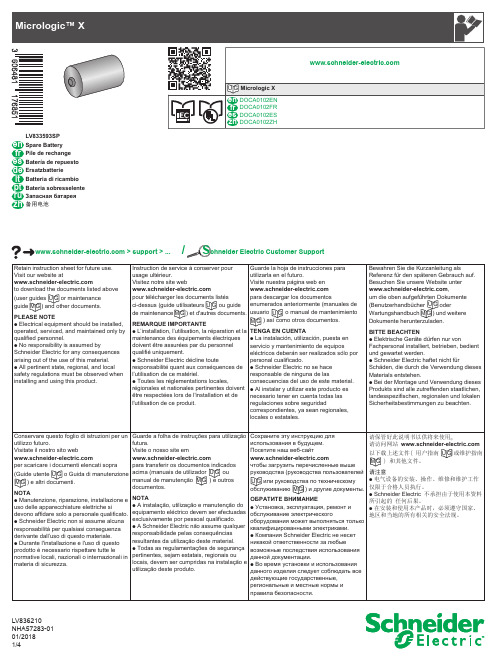
it pt zhru de es LV833593SP Spare Battery Pile de rechange Batería de repuesto ErsatzbatterieBatteria di ricambio Bateria sobresselente Запасная батарея备用电池fr enLV836210NHA57283-0101/20181/4 > support > ...NHA57283-012/4NHA57283-013/4In 1000 A Te stR eset 5In 1000 A Te stR es et 6O F 1O F 4O F 11O F 14O F 21O F 24In 1000 A 1Micrologic XIn 1000 A Te stR eset 89In 1000 A Te stR es et 7In 1000 A Te stR es et 2345V c 2.4A5V c 1.5A5V c 1ALV850067SPLV850055SPzh ruptit de esfr en La pile peut être remplacée quelque soit la position du disjoncteur, ouvert ou fermé.La batería se puede sustituir por el interruptor automático en posición abierta o cerrada.Die Batterie kann ersetzt werden,wenn sich der Leistungsschalter in einer offenen oder geschlossenen Position befindet.The battery may be replaced withthe circuit breaker in open or closed position.A bateria pode ser substituída com o disjuntor na posição aberta ou fechada.Заменять батарею можно, когда размыкатель цепи находится в разомкнутом или замкнутом положении.无论断路器处于分闸位置还是合闸位置,都可以更换电池 La batteria può essere sostituita con l'interruttore in posizione aperta o chiusa.3Installation / Installation / Instalación / Installation / Installazione / Instalação / Установка / 安装In 1000 A Te stR es et1In 1000 A Te stR eset In 1000 A Te stR es et 23RISQUE DE NON DÉTECTION DE LA NOUVELLE PILEAprès extraction de la pile déchargée, attendez 5 secondes avant d'installer la nouvelle pile.Si ces directives ne sont pas respectées, la nouvelle pile peut ne pas être détectée.HAZARD OF NON DETECTION OF NEW BATTERYAfter removing the dead battery, wait 5 seconds before installing the new battery. Failure to follow these instructions can result in the new battery not being detected.PERICOLO DI NON RILEVAMENTO NUOVA BATTERIA Dopo aver rimosso la batteria scarica, attendere 5 secondi prima di installare quella nuova.Il mancato rispetto di queste istruzioni può provocare il mancato rilevamento della nuova batteria.RIESGO DE NO DETECCIÓN DE LA NUEVA BATERÍADespués de retirar la batería agotada, espere 5 segundos antes de instalar la nueva.Si no se siguen estas instrucciones, es posible que la nueva batería no se detecte.GEFAHR DER NICHT-ERKENNUNG EINER NEUEN BATTERIEWarten Sie nach der Entnahme derverbrauchten Batterie 5 Sekunden, bevor Sie die neue Batterie einsetzen.Die Nichtbeachtung dieser Anweisungen kann zur Folge haben, dass die neue Batterie nicht erkannt wird.PERIGO DE NÃO DETEÇÃO DA NOVA BATERIADepois de retirar a bateria inoperativa, aguarde 5 segundos antes de instalar a nova bateria.O não cumprimento dessas instruções pode resultar na não deteção da nova bateria.ОПАСНОСТЬ НЕОБНАРУЖЕНИЯ НОВОЙ БАТАРЕИПосле удаления разряженной батареи выждите 5 секунд, прежде чем установить новую.Несоблюдение этой инструкции может привести к тому, что новая батарея не будет обнаружена.无法检测到新电池的风险移除旧电池之后,等待 5 秒钟,然后再安装新电池。
- 1、下载文档前请自行甄别文档内容的完整性,平台不提供额外的编辑、内容补充、找答案等附加服务。
- 2、"仅部分预览"的文档,不可在线预览部分如存在完整性等问题,可反馈申请退款(可完整预览的文档不适用该条件!)。
- 3、如文档侵犯您的权益,请联系客服反馈,我们会尽快为您处理(人工客服工作时间:9:00-18:30)。
—
1/1
— — 100 ns
8
8
8 1.35
UCC3807-1
2 (Int) — Prog.
—
—
1/1
— — 100 ns
8
8 1.50
UCC3807-2
2 (Int) — Prog.
—
—
1/1
— — 100 ns
8
8 1.50
UCC3807-3
2 (Int) — Prog.
—
—
1/1
Typical
Power
Level
Device
(W)
General-Purpose Single-Ended Controllers (Continued)
UCC38C43
10 to 250
UCC38C44
10 to 250
UCC38C45
10 to 250
(ഗॲ֖ຕჄฉᄻ)
AC/DCतDC/DCۉᇸׂ 19
PWMۉᇸ੦ഗ
Package(s)
MSOP SON SSOP TSSOP HTSSOP-PowerPAD™ SOIC SOIC-W (300 mil) SOIC-W Power PLCC DIL (PDIP)
Max
Device
VREF VREF Tol. (V) (%)
50 to 500
UC3524A
50 to 500
UC3525A/B
50 to 500
UC3526A
50 to 500
UC3825
50 to 750
UC3825A/B
50 to 750
UC3827-1/-2
50 to 500
UC3846
50 to 750
UC3856
50 to 750
UCC28089
25 to 250
UCC28220
50 to 800
UCC28221
50 to 800
UCC3806
50 to 750
UCC3808-1/-2/A-1/A-2
8 0.54
TL3845
52
50
— —
—
1/1
—— —
8/14
8 0.40
TL3845B
52
50
— —
—
1/1
—— —
8/14
8 0.54
UC28023
5.1 1
Prog.
—
—
1.5/1.5
—
—
16
16 1.35
UC3823
5.1 1
Prog.
—
1.5/1.5
—
—
16 20 16 1.60
Duty Cycle (%)
Soft Start E/A
Shut- Voltage down FeedPin forward
Output Drive
Leading
(Sink/Source) Slope Sync Edge
(A)
Comp Pin Blanking
Price*
Green Mode Controllers and Offline Bias Regulators
UCC2540
50 to 500
UCC3580-1/-2/-3/-4
50 to 500
UCC3583
50 to 500
UCC3960
25 to 250
UCC3961
25 to 250
Maximum Practical Frequency
1 MHz 1 MHz 1 MHz
50 to 500
UCC38083/4/5/6
50 to 500
UCC3810
50 to 500
Soft-Switching, ZVT and ZVS Controllers
UC3875/6/7
200 W to 2 kW
UC3879
200 W to 2 kW
— — 100 ns
8
8 1.50
UCC3809-1
55
90
—
—
0.8/0.4
—— — 8
8
8
8 0.85
UCC3809-2
55
90
—
—
UCC3813-0/1/2/3/4/5
51 2
1001
—
—
0.8/0.4 1/1
—— — 8 — — 100 ns
8
8
8
8
8 0.85 8 0.80
500 kHz 700 kHz 700 kHz 4 MHz 4 MHz
300 kHz 300 kHz 300 kHz 450 kHz 1 MHz 250 kHz 250 kHz 250 kHz 250 kHz 1 MHz 1 MHz 450 kHz 500 kHz 1 MHz 500 kHz 1 MHz/ch. 1 MHz/ch. 350 kHz 1 MHz 1 MHz 1 MHz
UC3823A/B
5.1 1
Prog.
—
2/2
—
—
16 20 16 4.90
UC3842/A
5 1.5 100
— —
—
1/1
—— —
8/14
8 0.80
UC3843
5 1.5 100
— —
—
1/1
—— —
8/14
8 0.80
UC3843A
5 1.5 100
— —
—
1/1
—— —
8/14
Topologies
(ഗॲ֖ຕჄူᄻ)
Voltage Mode Current Mode Avg. Current Mode Buck Boost Flyback (SEPIC, Cuk) Fwd (Including 2-Switch Fwd) Forward (D > 50%) Interleaved Fwd/Flyback/Boost Act-Clamp Fwd/Flyback Push-Pull I-Fed/V-Fed Push-Pull Half-Bridge Full-Bridge \-Shifted FB
— 22 mA
— 5 mA 14 mA 14 mA 22 mA 28 mA 32 mA 17 mA 17 mA 1.4 mA 3 mA 3 mA 1.4 mA 1 mA 20 mA 2 mA
7 to 40 7 to 40 7 to 40 8 to 40 9 to 30 8 to 40 8 to 40 8 to 40 8 to 35 9 to 30 9 to 22 8.4 to 20 8 to 40 8 to 40 8 to 15 8 to 14.5 8 to 14.5 7 to 15 4.3 to 15 8.3 to 15 8.3 to 11
Start-Up Current
50 μA 50 μA 50 μA
85 μA 130 μA 130 μA 50 μA 50 μA
— — — — 1.1 mA — 4 mA — — 1.1 mA 100 μA 1000 μA 1.5 mA 1.5 mA 130 μA 200 μA 500 μA 100 μA 130 μA 130 μA 150 μA
UCC2891/2/3/4
75 to 600
UCC2897
75 to 600
UCC3580-1/-2/-3/-4
50 to 500
UCC3895
200 W to 2 kW
Secondary-Side, Post Regulation
UC3824
50 to 250
100
— —
—
1/1
—— —
8/14
8 0.54
TL3843
52
100
— —
—
1/1
—— —
8/14
8 0.40
TL3843B
52
100
— —
—
1/1
—— —
8/14
8 0.54
TL3844
52
50
— —
—
1/1
—— —
8/14
8 0.40
TL3844B
52
50
— —
—
1/1
—— —
8/14
Dual Output Controllers
TL494
50 to 500
TL594
50 to 500
TL598
50 to 500
SG3524
50 to 500
UC28025
50 to 750
UC3524
8.4/7.6 14.5/9 8.4/7.6
1 mA 9.0 to 15 — 750 μA 9.0 to 15 — 750 μA 8.8 to 15 — 2.5 mA 8.2 to 15 — 2.5 mA 8.0 to 15 —
13.0/9 13.0/9 9.6/8.8 8.8/8.2 12/8
7.5 mA 12.4 mA 15 mA