OB2532_Demo Board Manual(3.5W)
2532中文资料

SWITCH-MODE TRANSFORMER GUIDE BY TECHNOLOGY
Ferrite
E30/15/7 ETD29X16X10 ETD29X15X10 ETD29X11X10 ETD34X13X11 ETD34X17X11 ETD39X17X13 ER48X18X18 ER54X20X18
This transformer is mainly intended to be used as a Resonant Switch-Mode Transformer for high-end 30” to 42” LCD TV sets with mains insulation. The most suitable circuit topology for this transformer is a half-bridge, quasi-resonant converter using ON Semiconductor’s ZVS controller MC34067. The common range of operation for this Switch-Mode Transformer is from 50-150 kHz.
9+9 6+6 6+6 8+8 7+7 9+9 9+9 7+7 11 +11 6+6 6+6
6+6
4+4 6+6 9+9 4+4 5+4 4+4 4+4 5+5 5+5 5+5 5+5 5+5 7+7
Slot Slot Slot Slot Slot Slot Slot Slot Slot Slot
OB产品LED照明应用

• • • • •
待机功耗 (0.28W @ 264VAC) 平均效率 88.28% @ 90-260VAC 轻载时关闭PFC节省待机功耗 PF 值 0.984 @ 230VAC 满载 精准输出OVP (ΔVovp/Vovp<5%)
19
On-Bright confidential
40W以上恒压方案(外置供电)
7
On-Bright confidential
OB2532方案10X1W LED
F1
R11
C6
85~264Vac
BD1
C1 R1
R5A/B
C3 R4 D5
D4
C9
R12
R2
R14 D7
R7 VDD GATE CS R8 COMP GND C5 INV Q1
D8 C4
R13 R10A/B
•
OB2532:MOS外置, 功率设计灵活,外置补 偿电路适用全电压输入 应用
5
On-Bright confidential
15W以下原边反馈Flyback驱动方案
•适用各型号LED灯杯
On-Bright confidential
6
15W以下低成本方案-OB253X系列
VDD 1 8 GND COMP 2 7 GND
INV
3
6
DRAIN
PWM控制器: SOT23-6:OB2532
40W以上恒压输出方案
•适用各型号路灯、隧道灯等大功率LED灯具应用
On-Bright confidential
17
40W以上恒压方案(外置供电)
•
方案1:OB6563+OB2203
18
On-Bright confidential
OB2532中文数据手册
kHz % V dB uA V V V nS nS
误差放大器部分
INV=2V,Comp=0V
VDD=16V,Io=20mA VDD=16V,Io=20mA
门驱动输出部分 VOL VOH V_clamp T_r T_f
注意:1、Freq_Max 表示 IC 内部的最大时钟频率。在系统应用中,60KHz 额定的最大工作 频率存在于最大输出功率或是恒压到恒流的转变点。
WW:周编号(01-52)
S:网络编号(可选的)源自引脚分配引脚号 1 2 3 4 5 6 引脚名 GND GATE CS INV COMP VDD I/O P O I I I P 描述 地 图腾柱门级驱动输出,驱动功率 MOSFET 电流检测输入,连接 MOSFET 电流检测电阻端 从辅助绕组来的电压反馈。连接到电阻分压器,反应输出电压 变化。占空比由误差放大器的输出和 3 脚的电流检测决定。 恒压稳定性的环路补偿 供电电源
应用
低功率 AC/DC 离线式开关电源用于 手机充电器 数字摄像机充电器 小功率适配器 个人电脑、电视等的辅助电源 线性调节器/RCC 替代 OB2532 提供 SOT23-6 封装
典型应用
一般信息
引脚结构 SOT23-6 封装引脚图如下所示
定购信息 器件号 OB2532MP
描述 SOT23-6,Pb-free,T&R
I_COMP_MAX
INV=0V,Comp=5V 频率抖动范围 EA 的参考电压 EA 的直流增益 最大电缆补偿电流 输出最低电平 输出最高电平 输出拑位电压电平 输出高电平时间 输出低电平时间
VDD=16V,CL=0.5nF VDD=16V,CL=0.5nF
14 +/-4 1.97 2 60 28 1 8 16 700 35 2.03
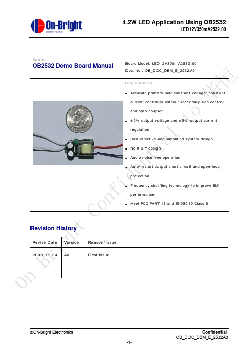
OB2532_Demo board_Manual_(4.2W)
Br i
gh t
Description RES SMD 0805 1M 5% RES SMD 1206 5.1M 5% RES SMD 0805 220R 5% RES SMD 1206 200K 5% RES SMD 1206 3.0R 1% RES SMD 0805 27K 1% RES SMD 0805 3.6K 1% RES SMD 0805 2.4K 1% RES SMD 0805 100R 5% EC 2.2uF/400V 105℃ φ6.3*11 CAP SMD 0805 2.2n F/250V CAP SMD 1206 10uF/25V CAP SMD 0603 220nF CAP SMD 0805 1.2nF
4.2W LED Application Using OB2532
LED12V350mA2532.00
Subject
OB2532 Demo Board Manual
Board Model: LED12V350mA2532.00 Doc. No.: OB_DOC_DBM_E_2532A0 Key features:
On
Br i
©On-Bright Electronics -2-
gh t
Co
8. EMI Test ...................................................................................................................................................11
Accurate primary-side constant voltage/ constant current controller without secondary side control
OB3350 Demo Board Manual_泰德_131030
fid Description:
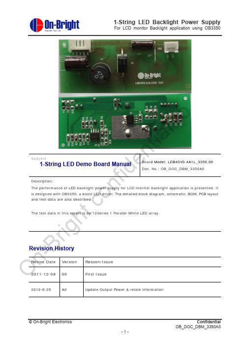
The performance of LED backlight power supply for LCD monitor backlight application is presented. It
n is designed with OB3350, a boost LED driver. The detailed block diagram, schematic, BOM, PCB layout o and test data are also described.
VIN=12V
德
l to 泰 CH1: GATE
CH3: CMP
CH2:ENA CH4:LED current
tia Startup through DIM signal
VIN=12V,
1-String LED Power Supply
For LCD monitor Backlight application using OB3350
2. Electrical Specification
2.1. Converter Specification
2.1.1. Input characteristics for Converter
Voltage output for LED driving
n 1
LED+
40V/400mA capability
o LED current return
On-Bright c 2
LED-
400mA capability
© On-Bright Electronics
Confidential OB_DOC_DBM_3350A0 -4-
ECS-2532HS中文资料

Description
Metal Ceramic
AuSn Tungsten (metalized)
Plating RoHS
Gold/Nickel (Surface)/(Under)
Compliant (Pb Free)
1105 South Ridgeview Road z Olathe, KS 66062 z Phone: 913.782.7787 z Fax: 913.782.6991 z
Stability -
Temperature
E = +/- 20 ppm F = +/- 15 ppm G = +/- 10 ppm
Blank = -30 ~ +85°C N = -40 ~ +85°C
1105 South Ridgeview Road z Olathe, KS 66062 z Phone: 913.782.7787 z Fax: 913.782.6991 z
SMD CLOCK OSCILLATOR
ECS-2018 (1.8V) subminiature SMD oscillators. Ideal for todays's high density applications.
TAPE DIMENSIONS (mm)
Package Data
Item
Lid Base Sealing Terminal
+T2e.6x6t T+2e.x8t +T2e.9x4t +T3.e1x3t5 T+3e.x3t +T3.e4x6t5
Option E
Text Text T±e2x0t Text Text T±e2x0t
OB2532A Datasheet_CN_佛山照明_111209

定购信息 型号 OB2532AMP
备注: 芯片的实际应用条件超出规定的“应用极限值”将会 对芯片造成永久性损伤。以上应用极限值标志了芯片可承 受应力等级, 但并不建议芯片在此极限条件或超出“推荐工 作条件”下工作。 芯片长时间处于最大额定工作条件, 会影 响芯片的可靠性。
lt
o
佛
应用极限参数 Parameter VDD 电压 VDD 稳压管钳位电流 COMP 电压 CS 输入电压 INV 输入电压 最小/最大工作结温 TJ 最小/最大储藏温度 Tstg 管脚焊接温度(10secs)
佛
40 80 Temperature(℃)
山 照
120
明
OB2532A
高精度原边 PWM 电源开关器
工作原理概述
OB2532A 是一款低系统成本的 LED 驱动控制 器,芯片工作在不连续(DCM)模式,应用于反 激隔离 LED 照明。采用原边反馈控制技术,无 需 TL431 和光耦等二次侧元器件, 其内置专利的 恒流(CC)控制技术,可以实现高精度的 LED 恒流输出特性,满足 LED 照明应用。 启动电流和启动控制 OB2532A 优化设计了启动电流(Typ. 5uA) ,当 VDD 电压经充电高于 UVLO(OFF)阈值电压, 芯片可以很快开启工作,因此在系统板上可以使 用高阻值的启动电阻来减小功率损耗。 工作电流 OB2532A 低至 2mA 的工作电流和多模式控制方 式可以实现系统的高转换效率和低待机功耗。 软启动 系统上电后,OB2532A 的内部软启动功能可以 减小 LED 电流过冲, 当 VDD 电压经充电高于 UVLO(OFF)阈值电压,芯片内部算法控制 CS 引脚峰值电压逐渐从 0V 增加到 0.8V,每次重启 都有软启动。 CC 工作原理 OB2532A 专利的 CC 控制需要工作在不连续模 式,应用于反激隔离 LED 照明(参考第 1 页典型 应用图)。LED 输出电流 Iout 计算公式: TDemag 与原边绕组电感量成反比例,控制 Lp 和开 关频率的乘积恒定不变,这样输出电流就不随原边 电感量的变化而变化。 芯片最大补偿原边电感量± 7% 偏差变化,实现 LED 恒流输出。 LED 输出电流计算公式:
OB2273 Demo Board Manual
2
3 Performance Evaluation..................................................................................................................... 10 3.1 Input Characteristics ................................................................................................................11 3.1. 1 Input current and Standby power ............................................................................................11 3.1. 2 Efficiency .................................................................................................................................11 3.2 Output Characteristics .............................................................................................................11 3.2.1 Line Regulation & Load Regulation..........................................................................................11 3.2.2 Ripple & Noise......................................................................................................................... 12 3.2.3 Overshoot & Undershoot ....................................................................................................... 13 3.2.4 Dynamic Test ......................................................................................................................... 14 3.2.5 Time Sequence...................................................................................................................... 14 3.3 Protections .............................................................................................................................. 15 3.3.1 Over Current Protection (OCP) ............................................................................................. 15 3.3.2 Over Voltage Protection (OVP).............................................................................................. 15 3.3.3 Over Load Protection (OLP) .................................................................................................. 16 3.3.4 Over Temperature Protection (OTP)...................................................................................... 16 3.4 EMI Test.................................................................................................................................. 17 3.4.1 Conduction EMI Test ............................................................................................................. 17 3.4.2 Radiation EMI Test ................................................................................................................ 18 4 Other important waveform ................................................................................................................. 19 4.1 CS, FB, Vdd & Vds waveform at no load/full load. ................................................................. 19 4.2 Vds waveform at full load, start/normal/output short............................................................... 19 4.2.1 VDS at full load, start/normal/output short .............................................................................. 19 4.2.2 Vds at full load, start waveform ............................................................................................... 20 4.2.3 Vds at full load, normal waveform ........................................................................................... 20 4.2.4 Vds at full load, output short waveform ................................................................................... 20
MKW2532中文资料
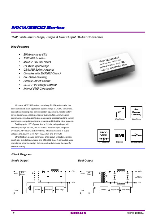
Dual OutputSingle OutputBlock DiagramMinmax's MKW2500 series, comprising 21 different models, has been conceived as an application specific range of DC/DC converters,specially addressing data communication equipments, mobile battery driven equipments, distributed power systems, telecommunication equipments, mixed analog/digital subsystems, process/machine control equipments, computer peripheral systems and industrial robot systems.Packing up to 15W of power into a 2x1x0.4 inch package, with efficiency as high as 86%, the MKW2500 has wide input ranges of 9-18VDC, 18-36VDC and 36-75VDC which is available in output voltages of 3.3V, 5V, 5.1V, 12V, 15V, {12V and {15VDC.Other feathers include continuous short circuit protection, remote on/off, six-sided shielded case and EN55022 Class A conducted noise compliance minimize design-in time, cost and eliminate the need for external filtering.yInternal SMD Constructiony UL 94V-0 Package Material y Remote On/Off Controly Six-Sided Shielding y Complies with EN55022 Class A y CSA1950 Safety Approvaly 2:1 Wide Input Range y MTBF > 700,000 Hours y 1500VDC Isolation y Efficiency up to 86%Key Features15W, Wide Input Range, Single & Dual Output DC/DC ConvertersMKW2500 SeriesREV:0 2005/04MINMAX18139330030005.1MKW254986363{50{500{15MKW254786363{62.5{625{12MKW254686363100100015MKW254486363125125012MKW25438238130030005MKW254278301026430030003.348( 36 ~ 75 )MKW25418178730030005.1MKW253986726{50{500{15MKW253786726{62.5{625{12MKW253686726100100015MKW253486726125125012MKW25338276230030005MKW253278402052830030003.324( 18 ~ 36 )MKW253181157430030005.1MKW2529861452{50{500{15MKW2527861452{62.5{625{12MKW2526861452100100015MKW2524861452125125012MKW252382152430030005MKW2522785030105730030003.312( 9 ~ 18 )MKW2521% (Typ.)mA (Typ.)mA (Typ.)mA (Typ.)mA mA VDC VDC@Max. Load @No Load @Max. Load Min.Max.EfficiencyReflected Ripple Current Input CurrentOutput CurrentOutput VoltageInput VoltageModel NumberModel Selection GuideEN55022 Class AConducted EMISix-Sided Shielded, Metal CaseRFIFree-Air ConvectionCooling %95---Humidity ]+125-50Storage Temperature ]+100-40CaseOperating Temperature ]+60-40Ambient Operating Temperature Unit Max.Min.Conditions ParameterEnvironmental SpecificationsExceeding the absolute maximum ratings of the unit could cause damage.These are not continuous operating ratings.mW5,000---Internal Power Dissipation]260---Lead Temperature (1.5mm from case for 10 Sec.)VDC 100-0.748VDC Input ModelsVDC 50-0.724VDC Input ModelsVDC 25-0.712VDC Input ModelsInput Surge Voltage( 1000 mS )Unit Max.Min.ParameterNotes :1. Specifications typical at Ta=+25], resistive load,nominal input voltage, rated output current unless otherwise noted.2. Transient recovery time is measured to within 1%error band for a step change in output load of 75%to 100%.3. Ripple & Noise measurement bandwidth is 0-20MHz.4. These power converters require a minimum output loading to maintain specified regulation.5. Operation under no-load conditions will not damage these modules; however, they may not meet all specifications listed.6. All DC/DC converters should be externally fused at the front end for protection.7. Other input and output voltage may be available,please contact factory.8. To order the converter with Remote On/Off function,please add a suffix -RC (e.g. MKW2521-RC).9. To order the converter with EN55022 Class A function, please add a suffix A (e.g. MKW2521A).10. Specifications subject to change without notice.Absolute Maximum RatingsMKW2500 Series2MINMAX REV:0 2005/04Pi FilterInput FiltermW 3500------Short Circuit Input Power A 1------All ModelsReverse Polarity Input Current 34292548V Input Models17151324V Input Models 8.58712V Input Models Under Voltage Shutdown36333048V Input Models18171524V Input Models VDC 98.5812V Input Models Start VoltageUnitMax.Typ.Min.Model ParameterInput SpecificationsContinuousOutput Short Circuit%/]{0.02{0.01---Temperature Coefficient %{4{2---Transient Response Deviation uS 500300---25% Load Step Change Transient Recovery Time %------120Over Power Protection mV rms 15------Ripple & Noise (20MHz)mV P-P 100------Over Line, Load & Temp Ripple & Noise (20MHz)mV P-P 8055---Ripple & Noise (20MHz)%{1.0{0.5---Io=10% to 100%Load Regulation %{0.5{0.1---Vin=Min. to Max.Line Regulation %{2.0{0.5---Dual Output, Balanced LoadsOutput Voltage Balance %{2.0{1.0---Output Voltage Accuracy Unit Max.Typ.Min.ConditionsParameterOutput SpecificationsK Hours------700MIL-HDBK-217F @ 25], Ground BenignMTBFKHz 400330290Switching Frequency pF 15001200---100KHz,1VIsolation Capacitance M[------1000500VDC Isolation Resistance VDC ------1650Flash Tested for 1 SecondIsolation Voltage Test VDC ------150060 SecondsIsolation Voltage Rated Unit Max.Typ.Min.Conditions ParameterGeneral SpecificationsReferenced to Negative InputControl CommonmA-1------Vin-RC=0V Control Input Current ( off )uA 50------Vin-RC=5.0V Control Input Current ( on )mA 10------Standby Input Current VDC 0.8----0.7Supply Off2.5 to 5.5VDC or Open CircuitSupply On Unit Max.Typ.Min.ConditionsParameterRemote On/Off ControlMKW2500 SeriesREV:0 2005/04MINMAX3# For each outputuF220220470470470470470Maximum Capacitive Load Unit {15V #{12V #15V 12V 5.1V 5V 3.3V Models by VoutCapacitive Load750mA Slow - Blow Type1250mA Slow - Blow Type2500mA Slow - Blow Type48V Input Models 24V Input Models 12V Input Models Input Fuse Selection GuideInput Voltage Transient RatingMKW2500 Series4MINMAX REV:0 2005/04MKW2500 SeriesREV:0 2005/04MINMAX5Test ConfigurationsInput Reflected-Ripple Current Test SetupInput reflected-ripple current is measured with a inductor Lin (4.7uH) and Cin (220uF, ESR < 1.0[ at 100 KHz) to simulate source impedance.Capacitor Cin, offsets possible battery impedance .Current ripple is measured at the input terminals of the module, measurement bandwidth is 0-500 KHz.Peak-to-Peak Output Noise Measurement TestUse a Cout 0.47uF ceramic capacitor.Scope measurement should be made by using a BNC socket, measurement bandwidth is 0-20 MHz. Position the load between 50 mm and 75 mm from the DC/DC Converter.Remote On/OffPositive logic remote on/off turns the module on during a logic high voltage on the remote on/off pin, and off during a logic low.To turn the power module on and off, the user must supply a switch to control the voltage between the on/off terminal and the -Vin terminal.The switch can be an open collector or equivalent.A logic low is -0.7V to 0.8V.A logic high is 2.5V to 5.5V.The maximum sink current at on/off terminal during a logic low is -1 mA.The maximum allowable leakage current of the switch at on/off terminal (2.5 to 5.5V) is 50uA.Overcurrent ProtectionTo provide protection in a fault (output overload) condition,the unit is equipped with internal current limiting circuitry and can endure current limiting for an unlimited duration. At the point of current-limit inception, the unit shifts from voltage control to current control. The unit operates normally once the output current is brought back into its specified range.Input Source ImpedanceThe power module should be connected to a low ac-impedance input source. Highly inductive source impedances can affect the stability of the power module.In applications where power is supplied over long lines and output loading is high, it may be necessary to use a capacitor at the input to ensure startup.Capacitor mounted close to the power module helps ensure stability of the unit, it is recommended to use a good quality low Equivalent Series Resistance (ESR < 1.0[ at 100KHz) capacitor of a 22uF for the 12V input devices and a 6.8uF for the 24V and 48V devices.MKW2500 Series6MINMAXREV:0 2005/04Output Ripple ReductionA good quality low ESR capacitor placed as close as practicable across the load will give the best ripple and noise performance.To reduce output ripple, it is recommended to use 4.7uF capacitors at the output.Maximum Capacitive LoadThe MKW2500 series has limitation of maximum connected capacitance at the output.The power module may be operated in current limiting mode during start-up, affecting the ramp-up and the startup time.For optimum performance we recommend 220uF maximum capacitive load for dual outputs and 470u F capacitive load for single outputs.The maximum capacitance can be found in the data sheet.Thermal ConsiderationsMany conditions affect the thermal performance of the power module, such as orientation, airflow over the module and board spacing. To avoid exceeding the maximum temperature rating of the components inside the power module, the case temperature must be kept below 100°C.The derating curves are determined from measurements obtained in an experimental apparatus.MKW2500 SeriesREV:0 2005/04MINMAX7The MKW2500 converter is encapsulated in a low thermal resistance molding compound that has excellent resistance/electrical characteristics over a wide temperature range or in high humidity environments.The encapsulant and unit case are both rated to UL 94V-0 flammability specifications.Leads are tin plated for improved solderability.UL94V-0:FlammabilityRemote On/Off (Optional)632g :Weight -Vout-Vout5Common No Pin 4Metal With Non-Conductive Baseplate :Case Material +Vout +Vout 3-Vin -Vin 2 2.0*1.0*0.4 inches+Vin +Vin 150.8*25.4*10.2 mm :Case Size Dual OutputSingle OutputPin Physical CharacteristicsPin Connections{0.002{0.05PinX.XXX{0.005X.XX{0.13Connecting Pin PatternsMechanical DimensionsMKW2500 Series8MINMAX REV:0 2005/04。
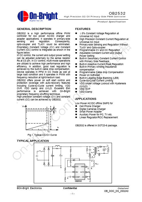
OB2532
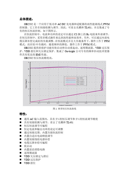
总体描述:OB2532是一个应用于低功率AC/DC充电器和适配器的高性能离线式PWM 控制器。
它工作在初级检测与调节。
因此,可省去光耦和TL431。
并且集成了专有的恒压恒流控制,如下图所示。
在恒流控制中,电流和功率的设定可以通过CS脚上的Rs电阻来外部调节。
在恒压控制中,采用多模式操作来达到高性能和高效率。
另外,可以通过内部电缆压降补偿完成好的负载调整。
在恒流模式并且大负载条件下,器件工作于PFM 模式,而在轻/中负载时,随着频率的降低,器件工作于PWM模式。
OB2532提供的保护功能有软启动和自动重起动、逐周期流限、VDD过压保护、VDD拑位和欠压锁定保护。
集成了On-bright公司专有的频率抖动技术使器件具有优良的EMI性能。
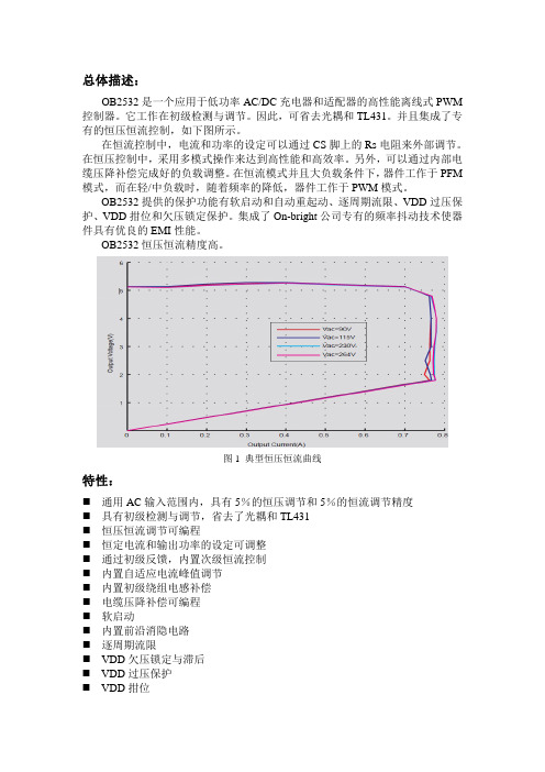
OB2532恒压恒流精度高。
图1 典型恒压恒流曲线特性:⏹通用AC输入范围内,具有5%的恒压调节和5%的恒流调节精度⏹具有初级检测与调节,省去了光耦和TL431⏹恒压恒流调节可编程⏹恒定电流和输出功率的设定可调整⏹通过初级反馈,内置次级恒流控制⏹内置自适应电流峰值调节⏹内置初级绕组电感补偿⏹电缆压降补偿可编程⏹软启动⏹内置前沿消隐电路⏹逐周期流限⏹VDD欠压锁定与滞后⏹VDD过压保护⏹VDD拑位应用低功率AC/DC 离线式开关电源用于 ⏹ 手机充电器⏹ 数字摄像机充电器 ⏹ 小功率适配器⏹ 个人电脑、电视等的辅助电源 ⏹ 线性调节器/RCC 替代 OB2532提供SOT23-6封装典型应用T一般信息引脚结构SOT23-6封装引脚图如下所示注意:漏级引脚连接到100mm PCB铜泊些或其它超过“推荐工作条件”的状态都不是默认的。
长时间工作在绝对最大额定状态会影响器件可靠性。
标记信息Y:年编号(0-9) WW:周编号(01-52) S:网络编号(可选的)引脚分配内部原理图电气特性注意:1、F req_Max表示IC内部的最大时钟频率。
在系统应用中,60KHz额定的最大工作频率存在于最大输出功率或是恒压到恒流的转变点。
恒流驱动芯片

3 LED 恒流驱动芯片之二:原边控制的PWM 控制器OB2532OB2532 是一种高性能的脱机PWM 控制器,输出功率低于15W,可以用作低功率的AC /DC 充电器和适配器,如手机、数码相机的充电器,PC 机和电视的辅助电源。
采用SOT23- 6 封装,有6 条引脚。
由于反馈控制来自原边,不存在隔离问题,因而无需像Viper12A /22A 那样,要用到光耦和稳压器TL431( 在图3 中使用了光耦H11AB17A 及双运放和基准电压TSM103) ,线路连接比较简单。
3. 1 驱动电路的特点(1) 全电压范围内有± 5% 的恒流调整精度,输出电流可以调节,可以设定输出功率;(2) 在原边控制下的副边恒流控制;(3) 自适应的峰值电流控制;(4) 内部有对原边绕组的电感补偿;(5) 可以对恒流及恒压值进行调整;(6) 电源接通时有软启动功能;(7) 电流检测有前沿消隐功能( LEB) ,无需外接滤波电路;(8) 能逐周对电流进行限制;(9)VDD 有欠电压封锁功能,且有回差。
OB2532 同Viper12A /22A 一样,也具有恒压(CV) 及恒流(CC) 输出特性,其特性可以用图8 的矩形曲线表示。
图8 OB2532 的输出矩形特性在恒流(CC) 控制下,输出功率可以通过CS 脚外接电阻RS( 也是MOS 管的源极电阻) 来调节;在恒压(CV) 控制下,为达到高效和提高性能的目的,可以有多种工作模式。
此外,由于内部有1 个对电缆压降进行补偿的线路,可以使负载具有很好的调整特性。
器件在恒流模式及大负载下,工作于脉频调制( PFM) 方式,而在轻负载/ 中等负载下,则降低频率,并工作于脉宽调制( PWM) 方式。
3. 2 OB2532 的引脚符号及功能它共有6 条引脚,其名称及功能如下:(1)GND———地;(2) GATE———为图腾柱输出,用来驱动外接的MOS 管;(3)CS———电流监测输入端,连到MOS 管源极的检测电阻上;(4) INV———误差放大器EA 的反相输入端,由变压器辅助绕组送来的反馈电压经电阻分压加于此端,它反映输出电压的大小,PWM 占空比取决于误差放大器EA 的输出及3 脚的电流监测信号;(5) COMP———EA 放大器的补偿端,接补偿电容,以使恒压输出保持稳定;(6)VDD———IC 的电源。
TiWi-uB2 EM BOARD User Guide
T I W I-U B2EM B OARDUser GuideLast updatedMay 28th, 2013Table of Contents1Introduction (3)1.1Purpose & Scope (3)1.2Applicable Documents (3)1.3Revision History (3)2TiWi-uB2 Module Description (4)3TiWi-uB2 EM Board Hardware (5)3.1Antenna (5)3.2Connectors (5)3.3Required Signals between EM Board and Host Device (6)3.4Connecting EM Board to Host Platform (7)3.5Power Supply (7)3.6Serial Interfaces (7)3.7HCI UART (8)3.8PCM Interface (8)3.9Option 1: Using EM Connectors (8)3.10Option 2: Using Single Row Headers (11)3.11Using J7 with USB to Serial Converter (12)4Schematic (13)4.1Bill Of Material (BOM) (14)5Application Development (15)5.1Overview (15)5.2Development Tools (15)6Contacting LS Research (20)1Introduction1.1 Purpose & ScopeThe purpose of this document is to provide details regarding the setup and use of theTiWi-uB2 module on an EM board. This document covers a description of the EM board and its features and a brief tutorial on how to operate the module EM board.1.2 Applicable Documents∙TiWi-uB2 Datasheet (330-0100)∙TiWi-uB2 Antenna Design Guide (330-0106)1.3 Revision HistoryTable 1 Revision History2TiWi-uB2 Module DescriptionThe TiWi-uB2 EM “Evaluation Module” Board is an evaluation platform for the LSResearch TiWi-uB2 Bluetooth and Bluetooth Low Energy (BLE) module.Communication between the TiWi-uB2 module, which is a slave, and the host device is through a UART interface.The TiWi-uB2 EM Board contains an on board chip antenna and U.FL connector. The EM board is intended for evaluation purposes when used in conjunction with variousTexas Instruments MSP430 and Stellaris development boards.Figure 1 TiWi-uB2 EM Board TopFigure 2 TiWi-uB2 EM Board Bottom3 TiWi-uB2 EM Board Hardware 3.1 AntennaThe TiWi-uB2 EM Board contains an on board chip antenna which is modular certified for FCC 15.247 and IC RSS-210, as well as compliant to the RF requirements for ETSI EN 300 328 and ETSI EN 301 489. The antenna layout and circuitry on the EM Board can be replicated on a custom designed PCB assembly. Assuming the design/layout is followed exactly as that which is on the EM Board, the custom PCB will retain the modular certification. Below are details on the certifications.FCC ID: TFB-BT1, 15.247 IC ID: 5969A-BT1, RSS 2103.2 ConnectorsThere are two primary connectors on the TiWi-uB2 EM Board (J1 & J2). These provide a standard interface to Texas Instruments development platforms (See Section 3.9). Two additional non populated connectors (J4 & J5) provide access to all of the significant signals on the module on a standard, single row 2mm pitch header.165423789Figure 3 TiWi-uB2 EM Board Top Side ConnectorsTable 2 TiWi-uB2 EM Board Top Side Connectors3.3 Required Signals between EM Board and Host DeviceIn addition to power and ground, there are three signals required for connecting a TiWi-uB2 module to a host device. See Table 3 below for details on these connections.Table 3 TiWi-uB2 Required Connections3.4 Connecting EM Board to Host PlatformThe TiWi-uB2 EM Board is intended to allow for evaluation of and early developmentwith a TiWi-uB2 module. The EM Board has two “EM” connectors on the bottom of the board that allows for easy connection to various Texas Instruments microcontrollerdevelopment platforms. The primary development platform is the MSP430F5438Experimenter Board.It is also possible to adapt the TiWi-uB2 EM Board to work with microcontroller platforms that do not have support for the EM connectors. Sections 3.9 and 3.10 describe the two options for adapting an EM Board to work with other microcontroller platforms.3.5 Power Supply3.5.1 VBATVBAT requires a 3.0V to 4.8V DC power supply.3.5.2 VDD_IOVDD_IO requires a 1.8V DC power supply.Figure 4 Power Supply3.6 Serial InterfacesThere are two serial interfaces to the module, HCI UART and PCM. Each interface isdescribed below.Figure 5 Serial Interfaces3.7 HCI UARTThis is the main interface between the host microcontroller and the module. TheBluetooth UART may also be used to download external patches from the host to theTiWi-uB2. The UART interface supports baud rates from 9600bps to 4Mbps.BT debug pin: The debug interface (TX_DBG) helps customers to debug the HW/SWissues for their application (not pictured).3.8 PCM InterfaceThe PCM Interface can connect to linear PCM Codec devices in master or slave mode.In master mode, the TiWi-uB2 generates the PCM_CLK and PCM_SYNC signals, and in slave mode, these signals are provided by another master on the PCM interface and are inputs to the TiWi-uB2.Figure 6 PCM Interface3.9 Option 1: Using EM ConnectorsEither build a PCB which has the EM Board mating connectors which will allow forplugging the TiWi-uB2 EM Board into, or solder wires to EM Board mating connectorsthat can then be wired into whatever development platform is being used.Below are two suggestions for the mating EM connectors.Through hole connector: Samtec TFM-110-01-S-D-WTSurface Mount connector: Samtec SFM-110-02-L-D-AIf building a PCB that has the mating EM Board connectors, the connectors need to be lined up and spaced 1.2” apart as shown in Figure 7.Figure 7 Host PCB EM Mating Connector Arrangement (Top View)Refer to Table 4 and Table 5 below for details on the signals brought out to the EM connectors J1 and J2.Table 4 EM Connector J1Table 5 EM Connector J2DI = Digital Input; DO = Digital Output; DIO = Digital Input/Output; PI = Power Input3.10 Option 2: Using Single Row HeadersSolder single row 12 pin 2mm headers into locations J4 and J5 on the EM Board, and then build a wiring harness between the headers on the EM Board and themicrocontroller development platform of interest.Below is a suggestion for the 12 pin 2mm headers.Sullins NRPN121PAEN-RCRefer to Table 6 and Table 7 below for details on the signals brought out to the single row headers J4 and J5.Table 6 Single Row Header J4DI = Digital Input; DO = Digital Output; PI = Power InputTable 7 Single Row Header J5DI = Digital Input; DO = Digital Output; DIO = Digital Input/Output; PI = Power Input3.11 Using J7 with USB to Serial ConverterJ7 is provided for interfacing the TiWi-uB2 Module to a USB-to-Serial converter, or similar serial device capable of providing 1.8V logic level data.Table 8 Single Row Header J7DI = Digital Input; DO = Digital Output; DIO = Digital Input/Output; PI = Power Input;4.1 Bill Of Material (BOM)Table 9 TiWi-uB2 EM Board BOM5Application Development5.1 OverviewThe TiWi-uB2 EM Board used in conjunction with a Bluetooth stack running on TI’sMSP430BT5438 or Stellaris LM3S9B96microcontroller (MCU) will reduce designbarriers and provides a highly flexible platform to enable customer’s early prototyping capabilities of embedded Bluetooth applications. The ready-to-go wireless platforms simplify the development process of pre-integrated and pre-validated Bluetooth serial link on an MSP430BT5438 or LM3S9B96system.For an overview of development platforms and software examples see CC256xBluetooth.5.2 Development Tools5.2.1 MSP430 HardwareHardware required for initial evaluation and development include:∙ 2 - TiWi-uB2 EM Boards∙ 1 - TI MSP430 USB Debugging Interface∙ 2 - TI MSP430F5438 Experimenter Boards5.2.2 Stellaris Hardware∙ 1 - TiWi-uB2 EM Board∙ 1 - TI MSP430 USB Debugging Interface∙ 1 - TI Stellaris LM3S9B96 EM2 Expansion Board∙ 1 - TI DK-LM3S9D965.2.3 SoftwareSoftware required for initial evaluation and development include:Stellaris∙Bluetopia®+LE SDK∙CC256x_Bluetopia_Stack∙Stellaris DK-LM3S9B96 SDKIntegrated BT Profiles∙Classic Bluetooth∙SPP∙A2DPFigure 9 TiWi-uB2 EM Board with Stellaris DK-LM3S9B96MSP430Bluetopia∙Bluetopia®+LE SDK∙CC256x_Bluetopia_Stack∙CC256x MSP430 Bluetopia Basic Demo APPSIntegrated BT Profiles∙Classic Bluetooth∙SPP∙Bluetooth Low Energy∙GATT∙ANP∙HRP∙HTP∙PASPThis Bluetooth software solution is licensed from Stonestreet One. The Bluetopia®+LE SDK is comprised of Single Mode and Dual Mode offering implementing the Bluetooth 4.0 specification. Bluetopia®+LE stack is built upon the solid foundation of the Bluetopia protocol stack that is currently being used in millions of consumer and industrial devices and that was first qualified in 2000 `TiWi-uB2 + MSP430 Bluetopia Basic Demo APPS allows users to evaluate TI's CC256x Bluetooth device by using the TiWi-uB2 EM board and the MSP-EXP430F5438 board. The CC256x+MSP430 Bluetooth sample applications code are provided to enable a rich out-of-box experience to the user. The application allows the user to use a console to send Bluetooth commands, setup a Bluetooth Device to accept connections, connect to a remote Bluetooth device and communicate over Bluetooth.Figure 10 TiWi-uB2 EM Board with MSP430F5438 Experimenter Board6Contacting LS ResearchHeadquarters LS Research, LLCW66 N220 Commerce CourtCedarburg, WI 53012-2636USATel: 1(262) 375-4400Fax: 1(262) 375-4248Website Wiki /products-wikiTechnical Support /products-forumSales Contact*************The information in this document is provided in connection with LS Research (hereafter referred to as “LSR”) products. No license, express or implied, by estoppel or otherwise, to any intellectual property right is granted by this document or in connection with the sale of LSR products. EXCEPT AS SET FORTH IN LSR’S TERMS AND CONDITIONS OF SALE LOCATED ON LSR’S WEB SITE, LSR ASSUMES NO LIABILITY WHATSOEVER AND DISCLAIMS ANY EXPRESS, IMPLIED OR STATUTORY WARRANTY RELATING TO ITS PRODUCTS INCLUDING, BUT NOT LIMITED TO, THE IMPLIED WARRANTY OF MERCHANTABILITY, FITNESS FOR A PARTICULAR PURPOSE, OR NON-INFRINGEMENT. IN NO EVENT SHALL LSR BE LIABLE FOR ANY DIRECT, INDIRECT, CONSEQUENTIAL, PUNITIVE, SPECIAL OR INCIDENTAL DAMAGES (INCLUDING, WITHOUT LIMITATION, DAMAGES FOR LOSS OF PROFITS, BUSINESS INTERRUPTION, OR LOSS OF INFORMATION) ARISING OUT OF THE USE OR INABILITY TO USE THIS DOCUMENT, EVEN IF LSR HAS BEEN ADVISED OF THE POSSIBILITY OF SUCH DAMAGES. LSR makes no representations or warranties with respect to the accuracy or completeness of the contents of this document and reserves the right to make changes to specifications and product descriptions at any time without notice. LSR does not make any commitment to update the information contained herein. Unless specifically provided otherwise, LSR products are not suitable for, and shall not be used in, automotive applications. LSR’s products are not intended, authorized, or warranted for use as components in applications intended to support or sustain life.Mouser ElectronicsAuthorized DistributorClick to View Pricing, Inventory, Delivery & Lifecycle Information:L S Research:450-0105。
BU2532AW资料

GENERAL DESCRIPTIONNew generation, high-voltage, high-speed switching npn transistor in a plastic envelope intended for use in horizontal deflection circuits of high resolution monitors.QUICK REFERENCE DATASYMBOL PARAMETERCONDITIONS TYP.MAX.UNIT V CESM Collector-emitter voltage peak value V BE = 0-1500V V CEO Collector-emitter voltage (open base)-800V I C Collector current (DC)-16A I CM Collector current peak value -40A P tot Total power dissipationT mb ≤ 25 ˚C-125W V CEsat Collector-emitter saturation voltage I C = 7.0 A; I B = 1.17 A - 5.0V I Csat Collector saturation current f = 82 kHz7-A t sStorage timeI Csat = 7.0 A; f = 82 kHz1.41.8µsPINNING - SOT429PIN CONFIGURATION SYMBOLLIMITING VALUESLimiting values in accordance with the Absolute Maximum Rating System (IEC 134)SYMBOL PARAMETERCONDITIONS MIN.MAX.UNIT V CESM Collector-emitter voltage peak value V BE = 0 V-1500V V CEO Collector-emitter voltage (open base)-800V I C Collector current (DC)-16A I CM Collector current peak value -40A I B Base current (DC)-10A I BM Base current peak value -15A -I B(AV)Reverse base currentaverage over any 20 ms period -200mA -I BM Reverse base current peak value 1-10A P tot Total power dissipation T mb ≤ 25 ˚C-125W T stg Storage temperature -55150˚C T jJunction temperature-150˚CTHERMAL RESISTANCESSYMBOL PARAMETERCONDITIONS TYP.MAX.UNIT R th j-mb Junction to mounting base -- 1.0K/W R th j-aJunction to ambientin free air45-K/W1 Turn-off current.STATIC CHARACTERISTICST mb = 25 ˚C unless otherwise specified SYMBOL PARAMETERCONDITIONSMIN.TYP.MAX.UNIT I CES Collector cut-off current 2V BE = 0 V; V CE = V CESMmax -- 1.0mA I CES V BE = 0 V; V CE = V CESMmax ;-- 2.0mA T j = 125 ˚CI EBO Emitter cut-off currentV EB = 7.5 V; I C = 0 A -- 1.0mA BV EBO Base-emitter breakdown voltage I B = 1 mA7.514-V V CEsat Collector-emitter saturation voltage I C = 7.0 A; I B = 1.17 A -- 5.0V V BEsat Base-emitter saturation voltage I C = 7.0 A; I B = 1.17 A 0.800.880.97Vh FE DC current gainI C = 1 A; V CE = 5 V 91727h FEI C = 7 A; V CE = 5 V6912.5DYNAMIC CHARACTERISTICST mb = 25 ˚C unless otherwise specified SYMBOL PARAMETERCONDITIONSTYP.MAX.UNIT Switching times (82 kHz line I Csat = 7.0 A; L C = 100 µH; C fb = 3 nF;deflection dynamic test circuit).V CC = 138 V; I B(end) = 1.0 At s Turn-off storage time 1.4 1.8µs t fTurn-off fall time0.060.1µs2 Measured with half sine-wave voltage (curve tracer).MECHANICAL DATA1. Refer to mounting instructions for SOT429 envelope.2. Epoxy meets UL94 V0 at 1/8".DEFINITIONSData sheet statusObjective specification This data sheet contains target or goal specifications for product development. Preliminary specification This data sheet contains preliminary data; supplementary data may be published later. Product specification This data sheet contains final product specifications.Limiting valuesLimiting values are given in accordance with the Absolute Maximum Rating System (IEC 134). Stress above one or more of the limiting values may cause permanent damage to the device. These are stress ratings only and operation of the device at these or at any other conditions above those given in the Characteristics sections of this specification is not implied. Exposure to limiting values for extended periods may affect device reliability. Application informationWhere application information is given, it is advisory and does not form part of the specification.© Philips Electronics N.V. 1997All rights are reserved. Reproduction in whole or in part is prohibited without the prior written consent of the copyright owner.The information presented in this document does not form part of any quotation or contract, it is believed to be accurate and reliable and may be changed without notice. No liability will be accepted by the publisher for any consequence of its use. Publication thereof does not convey nor imply any license under patent or other industrial or intellectual property rights.LIFE SUPPORT APPLICATIONSThese products are not designed for use in life support appliances, devices or systems where malfunction of these products can be reasonably expected to result in personal injury. Philips customers using or selling these products for use in such applications do so at their own risk and agree to fully indemnify Philips for any damages resulting from such improper use or sale.。
OB2538芯片中文资料
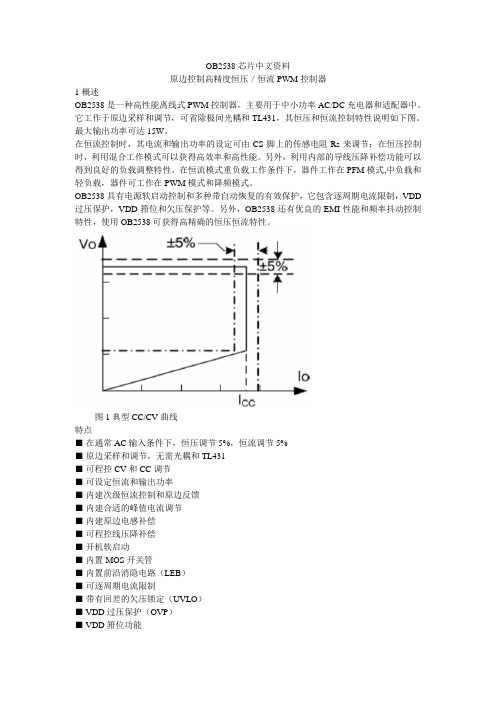
OB2538芯片中文资料原边控制高精度恒压/恒流PWM控制器1 概述OB2538是一种高性能离线式PWM控制器,主要用于中小功率AC/DC充电器和适配器中。
它工作于原边采样和调节,可省除极间光耦和TL431,其恒压和恒流控制特性说明如下图。
最大输出功率可达15W。
在恒流控制时,其电流和输出功率的设定可由CS脚上的传感电阻Rs来调节;在恒压控制时,利用混合工作模式可以获得高效率和高性能。
另外,利用内部的导线压降补偿功能可以得到良好的负载调整特性。
在恒流模式重负载工作条件下,器件工作在PFM模式,中负载和轻负载,器件可工作在PWM模式和降频模式。
OB2538具有电源软启动控制和多种带自动恢复的有效保护,它包含逐周期电流限制,VDD 过压保护,VDD箝位和欠压保护等。
另外,OB2538还有优良的EMI性能和频率抖动控制特性,使用OB2538可获得高精确的恒压恒流特性。
图1 典型CC/CV曲线特点■在通常AC输入条件下,恒压调节5%,恒流调节5%■原边采样和调节,无需光耦和TL431■可程控CV和CC调节■可设定恒流和输出功率■内建次级恒流控制和原边反馈■内建合适的峰值电流调节■内建原边电感补偿■可程控线压降补偿■开机软启动■内置MOS开关管■内置前沿消隐电路(LEB)■可逐周期电流限制■带有回差的欠压锁定(UVLO)■ VDD过压保护(OVP)■ VDD箝位功能应用中小功率AC/DC离线式开关电源■手机充电器■数码相机充电器■小功率适配器■ PC、TV等电器的辅助电源■线性调节器/替代RCC变换器■恒流LED照明封装形式:DIP8 典型应用引脚图引脚说明内部框图极限值电特性注:Freq_Max是指IC内部最大时钟频率,在系统应用里,60KHz的最大工作频率正常发生在最大输出功率或者从CV到CC状态的转换点。
特性曲线工作说明OB2538是一款成本低,效率高的PWM控制器,主要用于中小功率AC/DC转换器(电池充电器),适配器中,它可工作在原边反馈和调节中,无需光耦和TL431,内部的恒压和恒流特性控制可达到高精度CC/CV控制需要,完全可满足大多数适配器的应用需求,由于具有恒流特性,可用于LED照明。
OB2532 DataSheet

Ordering InformationPart NumberT&RPb-free,OB2532MP SOT23-6,DescriptionGroundTotem-pole gate drive output for power MOSFET.Current sense input. Connected to MOSFET current sensing resistor The voltage feedback from auxiliary winding. Connected to resistor divider from auxiliary winding reflecting output voltage. PWM duty cycle is determined by EA output and current sense signal at pin 3.Loop Compensation for CV StabilitySupplyPowerPvoltage is sampled at the end of the de-magnetization and it is hold until the next sampling. The sampled voltage is compared with Vref (2.0V) and the error is amplified. The error amplifier output COMP reflects the load condition and controls the PWM switching frequency to regulate the output voltage, thus constant output voltage can be achieved.When sampled voltage is below Vref and the error amplifier output COMP reaches its maximum, the switching frequency is controlled by the sampled voltage thus the output voltage to regulate the output current, thus the constant output current Adjustable CC point and Output PowerIn OB2532, the CC point and maximum output power can be externally adjusted by external current sense resistor Rs at CS pin as illustrated in Typical Application Diagram. The output power is adjusted through CC point change. The largerIMPORTANT NOTICERIGHT TO MAKE CHANGESOn-Bright Electronics Corp. reserves the right to make corrections, modifications, enhancements, improvements and other changes to its products and services at any time and to discontinue any product or service without notice. Customers should obtain the latest relevant information before placing orders and should verify that such information is current and complete.WARRANTY INFORMATIONOn-Bright Electronics Corp. warrants performance of its hardware products to the specifications applicable at the time of sale in accordance with its standard warranty. Testing and other quality control techniques are used to the extent it deems necessary to support this warranty. Except where mandated by government requirements, testing of all parameters of each product is not necessarily performed.On-Bright Electronics Corp. assumes no liability for application assistance or customer product design. Customers are responsible for their products and applications using On-Bright’s components, data sheet and application notes. To minimize the risks associated with customer products and applications, customers should provide adequate design and operating safeguards.LIFE SUPPORTOn-Bright Electronics Corp.’s products are not designed to be used as components in devices intended to support or sustain human life. On-bright Electronics Corp. will not be held liable for any damages or claims resulting from the use of its products in medical applications.MILITARYOn-Bright Electronics Corp.’s products are not designed for use in military applications. On-Bright Electronics Corp. will not be held liable for any damages or claims resulting from the use of its products in military applications.。
OB2532_DataSheet
Co nOrdering Information Part Number OB2532MP SOT23-6, Pb-free, T&RB ri g ht Co nf i dDescriptionGround Totem-pole gate drive output for power MOSFET. Current sense input. Connected to MOSFET current sensing resistorThe voltage feedback from auxiliary winding. Connected to resistordivider from auxiliary winding reflecting output voltage. PWM duty cycleis determined by EA output and current sense signal at pin 3.Loop Compensation for CV Stability P Power SupplyCo nf i de ni ah t C o f i de nt i a l toaitvoltage is sampled at the end of the de-magnetization and it is hold until the next sampling. The sampled voltage is compared with Vref (2.0V) and the error is amplified. The error amplifier output COMP reflects the load condition and controls the PWM switching frequency to regulate the output voltage, thus constant output voltage can be achieved.When sampled voltage is below Vref and the error amplifier output COMP reaches its maximum, the switching frequency is controlled by the sampled voltage thus the output voltage to regulate the output current, thus the constant output currentAdjustable CC point and Output PowerIn OB2532, the CC point and maximum output power can be externally adjusted by external current sense resistor Rs at CS pin as illustrated in Typical Application Diagram. The output power is adjusted through CC point change. The largerIMPORTANT NOTICERIGHT TO MAKE CHANGESOn-Bright Electronics Corp. reserves the right to make corrections, modifications, enhancements, improvements and other changes to its products and services at any time and to discontinue any product or service without notice. Customers should obtain the latest relevant information before placing orders and should verify that such information is current and complete.WARRANTY INFORMATIONOn-Bright Electronics Corp. warrants performance of its hardware products to the specifications applicable at the time of sale in accordance with its standard warranty. Testing and other quality control techniques are used to the extent it deems necessary to support this warranty. Except where mandated by government requirements, testing of all parameters of each product is not necessarily performed.On-Bright Electronics Corp. assumes no liability for application assistance or customer product design. Customers are responsible for their products and applications using On-Bright’s components, data sheet and application notes. To minimize the risks associated with customer products and applications, customers should provide adequate design and operating safeguards.LIFE SUPPORTOn-Bright Electronics Corp.’s products are not designed to be used as components in devices intended to support or sustain human life. On-bright Electronics Corp. will not be held liable for any damages or claims resulting from the use of its products in medical applications.MILITARYOn-Bright Electronics Corp.’s products are not designed for use in military applications. On-Bright Electronics Corp. will not be held liable for any damages or claims resulting from the use of its products in military applications.On -B ri g ht Co nf i de nt i a l to创裕。
HT2532应用指导

HT2532应用指导基于H T2532的15W反激电源适配器方案一.概要:HT2532是一款适用于低功率AC/DC电池充电器和电源适配器的高集成度和高性能的离线式PWM功率开关。
HT2532采用原边反馈技术,使系统应用中可以省去TL431和光耦,降低了成本。
全电压输入范围内恒压/恒流精度能保持在±5%以内。
CC/CV控制如图1所示。
在CC控制时,通过CS端的采样电阻Rs可调整输出功率和电流。
在CV控制时,多模式控制实现了高性能和高效率,而且,通过内置的可编程输出线压降补偿实现了好的负载调整率。
芯片在重载和CC控制时工作在PFM模式,在轻载和中载时工作在PWM模式,并且频率也会降低。
HT2532提供了软启动功能和多种全面的可恢复保护模式,其中包括:逐周期电流限制保护(OCP)、VCC电压的过压嵌位以及低压关闭(UVLO)。
其中,为了更好的保护内置高压功率MOSFET,栅极驱动输出电压被嵌位在12V。
HT2532在图腾柱栅极驱动输出端使用了频率抖动技术,可以很好的改善开关电源系统的EMI 性能。
HT2532芯片可以作为线性电源或者RCC模式电源的最佳替代产品,从而提高开关电源系统的整体性能,并有效地降低系统成本。
二.基本特性:·5uA超低的启动电流.·2mA低工作电流.·全电压输入范围内,具有5%的恒压调节和5%的恒流调节精度.·原边反馈技术使系统节省TL431和光耦.·可编程CV和CC调控.·内置原边绕组电感补偿. 图1: 典型CC/CV曲线·可编程的输出线压降补偿.·内置软启动.·内置前沿消隐电路.·逐周期电流限制保护(OCP)·VCC过压嵌位保护.·低电压关闭功能(UVLO).·栅极驱动输出电压嵌位(12V).·频率抖动功能.GND Gate INVCOMPCS VCC三.芯片内部模块图:图2: 内部结构图四.应用电路图:五.DEMO板实物图:图4: 正面视图图5: 反面视图六.电路原理:85V-264V交流输入电压VIN 经保险F1送入整流器D1~D4经л型滤电路C1、R3、L1、BC1、C2后输出120V-375VDC。
- 1、下载文档前请自行甄别文档内容的完整性,平台不提供额外的编辑、内容补充、找答案等附加服务。
- 2、"仅部分预览"的文档,不可在线预览部分如存在完整性等问题,可反馈申请退款(可完整预览的文档不适用该条件!)。
- 3、如文档侵犯您的权益,请联系客服反馈,我们会尽快为您处理(人工客服工作时间:9:00-18:30)。
Revision HistoryRevise DateVersionReason/Issue g ht Co nf ide nt i a l to创裕n -B ri g ht Co n创裕otlaN2 0.1622A253B-n230Vac/50HZ 66.6671.20 71.8872.7070.61Fig. 2 Efficiency vs. Percent of Rated Output Poweri g hnf i de nt i a l to创3.5W CC/CV Charger Module Using OB2532CH5V700mA2532.003.1.3. I-V Curve3.2.1. Line Regulation & Load RegulationTable. 3 Line Regulation & Load Regulation Input voltage No load Half load 90Vac/60HZ 5.118 5.225 115Vac/60HZ 5.115 5.224 230Vac/50HZ 5.086 5.200 264Vac/50HZ 5.058 5.190 Line Regulation 1.2% Load Regulation ±1.67%on fid3.2. Output Characteristicsen tFull load 5.099 5.098 5.095 5.094 Specification Test result <2% <±5% Pass Pass R&N (mV) Full load 84mV 84mV 81mV 81mV Fig. 6,7 Remark Fig. 4,5 Confidential OB_DOC_ DBM _A_253201 -11-Fig. 3 I-V CurveTable. 4nBrig3.2.2. Ripple & NoiseRipple & NoiseInput voltageht90Vac/60HZO115Vac/60HZ230Vac/50HZ 264Vac/50HZNote: Ripple& noise was measured at board end without probe cap and ground clip. Measurement bandwidth was limited to 20MHZ.©On-Bright ElectronicsCNo load 18.1mV 20mV 32mV 33mVialto创裕3.5W CC/CV Charger Module Using OB2532CH5V700mA2532.00Fig. 6 loadMeasured ripple& noise waveform@264Vac/50HZ, noon fidrigOver shoot and under shoot were measured under below conditions. a. AC input switch on for over shoot and off for under shoot. b. Input voltage ranges from 90Vac/60HZ~264Vac/50HZ. Table. 5 Over shoot & under shoot measurement results Input loadhtC3.2.3. Over Shoot & Under Shooten tFig. 7 load Measured ripple& noise waveform@264Vac/50HZ, fulliaRemark Fig. 8 Fig. 9 Fig. 10 Fig. 11 Full load No load Full load No load over shoot under shoot over shoot under shoot over shoot under shoot over shoot under shootOnB90V/60HZ264V/50HZ©On-Bright Electronics -12-ltConfidential OB_DOC_ DBM _A_253201oFig. 4 loadMeasured ripple& noise waveform@90Vac/60HZ, noFig. 5 loadMeasured ripple& noise waveform@90Vac/60HZ, full创裕3.5W CC/CV Charger Module Using OB2532CH5V700mA2532.00Fig. 8Measured overshoot waveform@90Vac/60HZ, full loadFig. 10 loadMeasured overshoot waveform@264Vac/50HZ, fullon fidOnBA dynamic loading with low set at 20% load lasting for 50ms and high set at 80% load lasting for 50mS is added to output. The ramp is set at 0.125A/us at transient. Measurement was taken at Board end(Same as R&N measurement) Table. 6 Output voltage under dynamic test Input Output (mV) Remark 264V/50HZ ±297mV Fig. 12 180V/50HZ ±297mV 115V/60HZ ±328mV 90V/60HZ ±328mV Fig. 13©On-Bright Electronics -13-rightC3.2.4. Dynamic Testen tFig. 11 load Measured overshoot waveform@264Vac/50HZ, noiaConfidential OB_DOC_ DBM _A_253201ltoFig. 9 loadMeasured overshoot waveform@90Vac/60HZ, no创裕3.5W CC/CV Charger Module Using OB2532CH5V700mA2532.00Table. 7OnBFig. 14 Turn on delay time measured waveform @100Vac/60HZ,full loadrightC©On-Bright Electronics -14-on fTurn-on delay/hold-up/rise/fall time measurement results Item Input voltage Meas. Data Test spec. 100V/60HZ 1.90S Turn-on delay time <2S 240V/50HZ 775.0mS 100V/60HZ 18.88mS Hold-up time >10mS 240V/50HZ N.A. 100V/60HZ 20.10mS Rise Time 240V/50HZ 17.19mS 100V/60HZ 6.89mS Fall Time 240V/50HZ 7.05mSia3.2.5. Time Sequence ( Full load)lt en tTest results Pass Pass Pass Pass Pass Pass Pass Remark Fig. 14 Fig. 15 Fig. 16 Fig. 17 Fig. 18 Fig. 19 Fig. 20Fig. 15 Turn on delay time measured waveform @240Vac/50HZ,full loadidoFig. 12 Output voltage waveform under Dynamic test @264Vac/50HZFig. 13 Output voltage waveform under Dynamic test @90Vac/60HZConfidential OB_DOC_ DBM _A_253201创裕3.5W CC/CV Charger Module Using OB2532CH5V700mA2532.00Fig. 16 loadHold-up time measured waveform@100Vac/60HZ,fullFig. 17 loadRise time measured waveform@100Vac/60HZ,fullFig. 18 loadRise time measured waveform@240Vac/50HZ,fullon fidOnBFig. 20©On-Bright Electronics -15-rigFall time measured waveform@240Vac/50HZ,full loadhtCen tFig. 19 load Fall time measured waveform@100Vac/60HZ,fulliaConfidential OB_DOC_ DBM _A_253201lto创裕3.5W CC/CV Charger Module Using OB2532CH5V700mA2532.003.3. EMI TestThe Power supply passed EN55022 Class B EMI requirement with more than 6dB margin3.3.1. Conducted EMI TestOnB©On-Bright Electronics -16-rightCon fiden tConfidential OB_DOC_ DBM _A_253201ialto创裕3.3.1.1. EN55022 CLASS B @ full load report3.5W CC/CV Charger Module Using OB2532CH5V700mA2532.00 3.3.1.2. FCC CLASS B @ full load reportOnB©On-Bright Electronics -17-rightCon fiden tConfidential OB_DOC_ DBM _A_253201ialto创裕3.5W CC/CV Charger Module Using OB2532CH5V700mA2532.003.3.2. Radiation EMI Test3.3.2.1. EN55022 CLASS B @ full load report3.3.2.2. FCC CLASS B @ full load reportOnB©On-Bright Electronics -18-rightCon fiden tConfidential OB_DOC_ DBM _A_253201ialto创裕3.5W CC/CV Charger Module Using OB2532CH5V700mA2532.004. Protection Function4.1. Over voltage protectionTable. 8 OVP @ no loadInput 115Vac/60Hz 230Vac/50Hz OVP Protection OK OK4.2. Short circuit protectionTable. 9OnB©On-Bright Electronics -19-rightCOLP @ Full load Input 115Vac/60Hz 230Vac/50Hzon f4.3. Open Loop ProtectionidFig. 21Output short, Vds waveform@90 Vac/60Hz, full loaden tFig. 22Output short, Vds waveform@264 Vac/50Hz, full loadiaOLP Protection OK OK Confidential OB_DOC_ DBM _A_253201lto创The system is protected during output short circuit condition and recovered when short circuit condition is removed.裕3.5W CC/CV Charger Module Using OB2532CH5V700mA2532.005. Thermal TestingVin 85Vac/60Hz 230Vac/50Hz 264Vac/50Hz Po 3.5W 3.5W 3.5W Environment 40℃ 40℃ 40℃ Case(inside) 63.1℃ 66.0℃ 66.5℃ MOS 82.0℃ 87.5℃ 89.5℃ Transformer(winding ) 74.5℃ 78.0℃ 78.2℃Note: All data were be measured at #24(1.8m)Line end Case: Φ60mmX25mmX42mmOnB©On-Bright Electronics -20-rightCon fiden tConfidential OB_DOC_ DBM _A_253201ialto创裕Fig. 23 Vdd, Sense&Vds waveform@90Vac/60Hz,no load Fig. 24 Vdd, Sense & Vds waveform @90Vac/60Hz, full loadFig. 26 Vdd, Sense & Vds waveform @264Vac/50Hz,full loadMOSFET Vds waveform @ start/normal/output shortFig. 27 Start, Vds waveform@90 Vac/60Hz, full loadFig. 28 Start, Vds waveform@264 Vac/50Hz, full loadOn -B ri g hCo nf i de nt i a l to创裕Fig. 30 Normal, Vds waveform@264 Vac/50Hz, full loadFig. 32 Output short, Vds waveform@264 Vac/50Hz-B ri g ht Co f i de nt i a l to创裕。
