FPGA可编程逻辑器件芯片XC2V80-5FG456C中文规格书
FPGA可编程逻辑器件芯片XC2S100-5FGG456C中文规格书
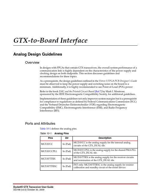
GTX-to-Board InterfaceAnalog Design GuidelinesOverviewIn designs with FPGAs that contain GTX transceivers, the overall system performance of acommunication link is highly dependent on the characteristics of the power supply andclocking design on both endpoints. This section discusses guidelines andrecommendations for these topics.As a prerequisite, the design guidelines outlined in the Virtex-5 FPGA PCB Designer’s Guidemust be observed to keep the power supply and switching noise on the board to aminimum. Additionally, it is highly recommended to use Point-of-Load (POL) powerRefer to the book EMC and the Printed Circuit Board[Ref7] by Mark I. Montrose,sponsored by the IEEE Electromagnetic Compatibility Society, for additional guidelines.Implementation of these guidelines not only improves system margins but is a prerequisitefor compliance to regulations as defined by Federal Communications Commission (FCC)and the Verband Deutscher Elektrotechniker (VDE) regarding ElectromagneticCompatibility (EMC), Electromagnetic Interference (EMI), and Radio FrequencyInterference (RFI).Ports and AttributesTable10-1 defines the analog pins.Table 10-1:Analog PinsPins Dir DescriptionMGTAVCC In (Pad)MGTAVCC is the analog supply for the internal analog circuits of the GTX_DUAL tile.MGTAVCCPLL In (Pad)MGTAVCCPLL is the analog supply for the shared PMA PLL of the GTX_DUAL tile.MGTAVTTRX In (Pad)MGTAVTTRX is the analog supply for the receiver circuits and termination of the GTX_DUAL tile.MGTAVTTRXC In (Pad)FXT only: MGTAVTTRXC is the analog supply for resistor calibration and standby circuit of the entire device.Chapter 10:GTX-to-Board InterfaceTable 10-2 defines the analog attributes.MGTAVTTRXC_RIn (Pad)TXT only: MGTAVTTRXC_R is the analog supply for resistor calibration and standby circuit of the right transceiver column.MGTAVTTRXC_L In (Pad)TXT only: MGTAVTTRXC_L is the analog supply for resistor calibration and standby circuit of the left transceiver column.MGTAVTTTX In (Pad)MGTAVTTTX is the analog supply for the transmittertermination and driver circuits and reference clock routing of the GTX_DUAL tile.MGTREFCLKP MGTREFCLKN In (Pad)Differential clock input pin pair (1) for the reference clock of the GTX_DUAL tile.MGTRREF In (Pad)FXT only: MGTRREF is the reference resistor input for the entire device.MGTRREF_R In (Pad)TXT only: MGTRREF_R is reference resistor input for the right transceiver column.MGTRREF_LIn (Pad)TXT only: MGTRREF_L is reference resistor input for the left transceiver column.Notes:1.This clock can only be accessed by the FPGA logic through the REFCLKOUT port.Table 10-2:Analog AttributesAttributeTypeDescriptionCLKINDC_BBooleanMust be set to TRUE. Oscillators driving the dedicated reference clock inputs must be AC coupled.When set to FALSE for testing, the common mode voltage of the driving circuit must match the common mode voltage of the differential clock input pair (MGTCLKP , MGTCLKN). The differential swing must not exceed the maximum differential swing of the clock input pair.(1, 2)CLKRCV_TRST BooleanWhen set to FALSE, switches off the internal termination resistors of the differential clock input pair. This results in a high-impedance input characteristic that is only intended for testing.When set to TRUE, the differential clock input pair is terminated with a 100Ω differential impedance. Each clock input in (MGTCLKP , MGTCLKN) is contacted via a 50Ω resistor to a midterm nominal voltage of 0.8V .(1, 2)TERMINATION_CTRL[4:0]5-bit BinaryControls the internal termination calibration circuit. Refer to Table 10-5, page 259 for encoding.Table 10-1:Analog Pins (Cont’d)PinsDir DescriptionResistor Calibration CircuitResistor Calibration CircuitThe resistor calibration circuit in the GTX transceiver is used to precisely calibrate the TX and RX termination resistors via an external precision reference resistor.Table 10-1 defines the resistor calibration circuit pins used for TX and RX termination resistor calibration.TERMINATION_IMP_0TERMINATION_IMP_1IntegerSelects the termination impedance for the TX driver and receiver.See Figure 10-4 calibrating the impedancevalues. Always set to 50, which selects the 50Ω termination impedance. The RocketIO™ GTX Transceiver Wizard automatically sets the TERMINATION_IMP_(0/1) attributes to 50.TERMINATION_OVRD BooleanSelects whether the external 59Ω(3)precision resistor connected to the MGTRREF pin or an override value is used, as defined by TERMINATION_CTRL[4:0].Notes:1.Violation of the rules outlined in this section result in a marginal or dysfunctional design, device degradation in the future, or device damage.2.Consult DS202: Virtex-5 FPGA Data Sheet for the common mode voltage values and the associated differential swing and operating conditions.3.The nominal value of the external precision resistor RREF connected to the MGTRREF pin is different for LXT/SXT devices and FXT/TXT devices. For LXT/SXT devices with GTP_DUAL tiles, RREF is 50Ω nominal. For FXT/TXT devices with GTX_DUAL tiles, RREF is 59Ω nominal.Table 10-2:Analog Attributes (Cont’d)AttributeTypeDescriptionTable 10-3:Resistor Calibration Circuit PinsPinsDir DescriptionMGTAVTTRXC In (Pad)FXT only: MGTAVTTRXC is the analog supply for resistor calibration and standby circuit of the entire device.MGTAVTTRXC_LIn (Pad)TXT only: MGTAVTTRXC_L is the analog supply for resistor calibration and standby circuit of the left transceiver column.MGTAVTTRXC_R In (Pad)TXT only: MGTAVTTRXC_R is the analog supply for resistor calibration and standby circuit of the right transceiver column.MGTRREF In (Pad)FXT only: MGTRREF is the reference resistor input for the entire device.MGTRREF_L In (Pad)TXT only: MGTRREF_L is reference resistor input for the left transceiver column.MGTRREF_RIn (Pad)TXT only: MGTRREF_R is reference resistor input for the right transceiver column.Chapter 10:GTX-to-Board InterfaceResistor Calibration Circuit。
FPGA可编程逻辑器件芯片XC2S100-5FGG456I中文规格书
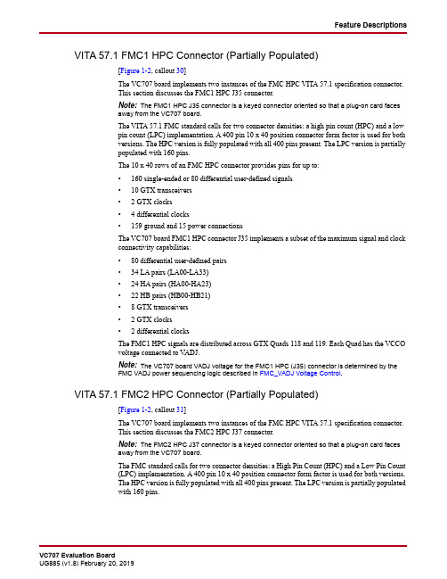
Feature DescriptionsVITA 57.1 FMC1 HPC Connector (Partially Populated)[Figure1-2, callout 30]The VC707 board implements two instances of the FMC HPC VITA 57.1 specification connector.This section discusses the FMC1 HPC J35 connector.Note:The FMC1 HPC J35 connector is a keyed connector oriented so that a plug-on card facesaway from the VC707 board.The VITA 57.1 FMC standard calls for two connector densities: a high pin count (HPC) and a lowpin count (LPC) implementation. A 400 pin 10x40 position connector form factor is used for bothversions. The HPC version is fully populated with all 400 pins present. The LPC version is partiallypopulated with 160 pins.The 10x40 rows of an FMC HPC connector provides pins for up to:•160 single-ended or 80 differential user-defined signals•10 GTX transceivers• 2 GTX clocks• 4 differential clocks•159 ground and 15 power connectionsThe VC707 board FMC1 HPC connector J35 implements a subset of the maximum signal and clockconnectivity capabilities:•80 differential user-defined pairs•34 LA pairs (LA00-LA33)•24 HA pairs (HA00-HA23)•22 HB pairs (HB00-HB21)•8 GTX transceivers• 2 GTX clocks• 2 differential clocksThe FMC1 HPC signals are distributed across GTX Quads 118 and 119. Each Quad has the VCCOvoltage connected to V ADJ.Note:The VC707 board VADJ voltage for the FMC1 HPC (J35) connector is determined by theFMC VADJ power sequencing logic described in FMC_VADJ Voltage Control.VITA 57.1 FMC2 HPC Connector (Partially Populated)[Figure1-2, callout 31]The VC707 board implements two instances of the FMC HPC VITA 57.1 specification connector.This section discusses the FMC2 HPC J37 connector.Note:The FMC2 HPC J37 connector is a keyed connector oriented so that a plug-on card facesaway from the VC707 board.The FMC standard calls for two connector densities: a High Pin Count (HPC) and a Low Pin Count(LPC) implementation. A 400pin 10x40 position connector form factor is used for both versions.The HPC version is fully populated with all 400 pins present. The LPC version is partially populatedwith 160 pins.Chapter 1:VC707 Evaluation Board FeaturesFeature DescriptionsC2FMC1_HPC_DP0_C2M_P (1)E2D1PWRCTL1_VCC4B_PG AL32C3FMC1_HPC_DP0_C2M_N (1)E1D4FMC1_HPC_GBTCLK0_M2C_P (1)A10C6FMC1_HPC_DP0_M2C_P (1)D8D5FMC1_HPC_GBTCLK0_M2C_N (1)A9C7FMC1_HPC_DP0_M2C_N (1)D7D8FMC1_HPC_LA01_CC_P LVCMOS18J40C10FMC1_HPC_LA06_P LVCMOS18K42D9FMC1_HPC_LA01_CC_N LVCMOS18J41C11FMC1_HPC_LA06_N LVCMOS18J42D11FMC1_HPC_LA05_P LVCMOS18M41C14FMC1_HPC_LA10_P LVCMOS18N38D12FMC1_HPC_LA05_N LVCMOS18L41C15FMC1_HPC_LA10_N LVCMOS18M39D14FMC1_HPC_LA09_P LVCMOS18R42C18FMC1_HPC_LA14_P LVCMOS18N39D15FMC1_HPC_LA09_N LVCMOS18P42C19FMC1_HPC_LA14_N LVCMOS18N40D17FMC1_HPC_LA13_P LVCMOS18H39C22FMC1_HPC_LA18_CC_P LVCMOS18M32D18FMC1_HPC_LA13_N LVCMOS18G39C23FMC1_HPC_LA18_CC_N LVCMOS18L32D20FMC1_HPC_LA17_CC_P LVCMOS18L31C26FMC1_HPC_LA27_P LVCMOS18J31D21FMC1_HPC_LA17_CC_N LVCMOS18K32C27FMC1_HPC_LA27_N LVCMOS18H31D23FMC1_HPC_LA23_P LVCMOS18P30C30FMC1_HPC_IIC_SCL U52.4D24FMC1_HPC_LA23_N LVCMOS18N31C31FMC1_HPC_IIC_SDA U52.3D26FMC1_HPC_LA26_P LVCMOS18J30C34GA0=0=GND D27FMC1_HPC_LA26_N LVCMOS18H30C35VCC12_P D29FMC1_HPC_TCK_BUF U19.14C37VCC12_P D30FMC_TDI_BUF U19.18C39VCC3V3D31FMC1_TDO_FMC2_TDI U27.2D32VCC3V3D33FMC1_HPC_TMS_BUF U19.17D34NCD35GA1=0=GND D36VCC3V3D38VCC3V3D40VCC3V3J35 FMC 1HPC PinSchematic Net NameI/OStandardU1 FPGAPinJ35FMC 1 HPC PinSchematic Net NameI/O StandardU1 FPGA PinJ2NC K1NC J3NCK4NC J6FMC2_HPC_HA03_P LVCMOS18AA29K5NCJ7FMC2_HPC_HA03_N LVCMOS18AA30K7FMC2_HPC_HA02_P LVCMOS18AC30J9FMC2_HPC_HA07_P LVCMOS18AC31K8FMC2_HPC_HA02_N LVCMOS18AD30J10FMC2_HPC_HA07_N LVCMOS18AD31K10FMC2_HPC_HA06_P LVCMOS18AB31J12FMC2_HPC_HA11_P LVCMOS18AE34K11FMC2_HPC_HA06_N LVCMOS18AB32J13FMC2_HPC_HA11_N LVCMOS18AE35K13FMC2_HPC_HA10_P LVCMOS18AF31J15FMC2_HPC_HA14_P LVCMOS18AF35K14FMC2_HPC_HA10_N LVCMOS18AF32J16FMC2_HPC_HA14_N LVCMOS18AF36K16FMC2_HPC_HA17_CC_P LVCMOS18AC34J18FMC2_HPC_HA18_P LVCMOS18AB36K17FMC2_HPC_HA17_CC_N LVCMOS18AD35J19FMC2_HPC_HA18_N LVCMOS18AB37K19FMC2_HPC_HA21_P LVCMOS18AA34J21FMC2_HPC_HA22_P LVCMOS18Y35K20FMC2_HPC_HA21_N LVCMOS18AA35J22FMC2_HPC_HA22_N LVCMOS18AA36K22FMC2_HPC_HA23_P LVCMOS18Y37J24FMC2_HPC_HB01_P LVCMOS18AM16K23FMC2_HPC_HA23_N LVCMOS18AA37J25FMC2_HPC_HB01_N LVCMOS18AN16K25FMC2_HPC_HB00_CC_P LVCMOS18AT17J27FMC2_HPC_HB07_P LVCMOS18BB19K26FMC2_HPC_HB00_CC_N LVCMOS18AU17J28FMC2_HPC_HB07_N LVCMOS18BB18K28FMC2_HPC_HB06_CC_P LVCMOS18AY18J30FMC2_HPC_HB11_P LVCMOS18AM18K29FMC2_HPC_HB06_CC_N LVCMOS18AY17J31FMC2_HPC_HB11_N LVCMOS18AM17K31FMC2_HPC_HB10_P LVCMOS18AP20J33FMC2_HPC_HB15_P LVCMOS18AL19K32FMC2_HPC_HB10_N LVCMOS18AR19J34FMC2_HPC_HB15_N LVCMOS18AM19K34FMC2_HPC_HB14_P LVCMOS18AK19J36FMC2_HPC_HB18_P LVCMOS18AJ18K35FMC2_HPC_HB14_N LVCMOS18AK18J37FMC2_HPC_HB18_NLVCMOS18AJ17K37FMC2_HPC_HB17_CC_P LVCMOS18AW18K38FMC2_HPC_HB17_CC_N LVCMOS18AW17J39FMC2_VIO_B_M2CBANK 32 VCCOK40FMC2_VIO_B_M2CBANK 32VCCONotes:1.No I/O standards are associated with MGT connections.J37 FMC 2HPC PinSchematic Net NameI/O Standard U1 FPGA PinJ37FMC 2 HPC PinSchematic Net NameI/O Standard U1 FPGA Pin。
FPGA可编程逻辑器件芯片XC2V1000-5FGG456C中文规格书

Table 2: Enabling Bidirectional Datapath ControlControl MechanismRelated Attributes Gating •RX datapath gating: The RX_GATING attribute enables gating of the RX datapath based on the PHY_RDEN port.While RX_GATING enables gating, the CONTINUOUS_DQS attribute lets users choose between PHY_RDEN operating based in the PLL_CLK or the strobe clock domain.•TX datapath gating: The TX_GATING attribute enables gating of the TX datapath based on the PHY_WREN port (which is serialized but not inverted when used for gating) and PHY_WREN operates in the PLL_CLK domain.NIBBESLICE[1] cannot be gated.Tristating •Tristating: The TBYTE_CTL_# attribute determines whether tristating is controlled by the T (combinatorial)port or an inverted and serialized PHY_WREN port (which is in the PLL_CLK domain).T_OUT[5:0] is the tristate control output from the XPHY. Each bit of T_OUT is associated with a NIBBLESLICE, and TBYTE_CTL_# allows each NIBBLESLICE to select its corresponding T_OUT bit to be controlled by either T or PHY_WREN. In other words for a NIBBLESLICE[x], T_OUT[x]reflects the tristate control input selected by TBYTE_CTL_x. If TBYTE_CTL_x = T, T_OUT[x](associated with NIBBLESLICE[x]) is controlled via the T[x] input. Because this is a combinatorial route, T_OUT[x] is not aligned to the data. If TBYTE_CTL_x = PHY_WREN, T_OUT[x] (associated with NIBBLESLICE[x]) is controlled through the PHY_WREN port. This input is inverted,serialized, and output synchronously (through T_OUT[x]) with the TX data when used for tristating. For more information, see Controlling Tristate Control .IMPORTANT! When using 2:1 serialization (TX_DATA_WIDTH = 2), each NIBBLESLICE tristate buffer can only be controlled through the combinatorial T input (TBYTE_CTL_<0-5> = T). Tristate control through the PHY_WREN input (TBYTE_CTL_x = PHY_WREN) is only possible for 8:1 and 4:1 serialization(TX_DATA_WIDTH = 8 and 4, respectively).PHY_RDEN is set up and used to control RX datapath gating is as follows:•PHY_RDEN controls accepting or rejecting the strobe entering on NIBBLESLICE[0] or from inter-byte or inter-nibble clocking, depending upon the settings of CONTINUOUS_DQS,RX_GATING, and RX_DATA_WIDTH. Always ensure the strobe has stabilized and BISC has completed before asserting PHY_RDEN. Refer to Controlling Built-in Self-Calibration for when BISC is considered completed.•When RX_DATA_WIDTH = don't care, RX_GATING = ENABLE, and CONTINUOUS_DQS =TRUE, then the four bits of PHY_RDEN are OR'd together and that output is used to control the gate. If the result of the OR operation is 1, the capture clock is accepted. If it is 0, then the capture clock is rejected. PHY_RDEN is synchronized to the capture clock for this attribute combination. When CONTINUOUS_DQS = TRUE, send 3 capture clock cycles before sending data.Chapter 2: XPHY Architecture•When RX_DATA_WIDTH = 4 or 8, RX_GATING = ENABLE, and CONTINUOUS_DQS = FALSE, set the following bits of PHY_RDEN to 1 to accept the strobe or 0 to reject the strobe.PHY_RDEN is synchronized to PLL_CLK for this attribute combination. Each bit of PHY_RDEN controls two UI worth of data:○If RX_DATA_WIDTH = 8: [3:0]○If RX_DATA_WIDTH = 4: [2][0]○If RX_DATA_WIDTH = 2: not supported•When RX_GATING = DISABLE the gate is always open, regardless of the value of RX_DATA_WIDTH, CONTINUOUS_DQS, or PHY_RDEN. In this scenario (RX_GATING = DISABLE), the strobe starts the deserialization in the RX datapath. Because of this, the strobe must be stable to ensure XPHY alignment.•When SERIAL_MODE = TRUE, tie all four bits of PHY_RDEN HighPHY_WREN is set up and used to control TX datapath gating as follows:•When TX_GATING = ENABLE, PHY_WREN gates the TX datapath of NIBBLESLICE[0], NIBBLESLICE[2], NIBBLESLICE[3], NIBBLESLICE[4], and NIBBLESLICE[5]. NIBBLESLICE[1] cannot be gated. Set the following bits of PHY_WREN to 0 to gate transmit data or 1 to not gate transmit data:○If TX_DATA_WIDTH = 8: [3:0]○If TX_DATA_WIDTH = 4: [2][0]○If TX_DATA_WIDTH = 2: not supported•Note that PHY_WREN can be used to control both TX datapath gating (if TX_GATING = ENABLE) and tristating (if TBYTE_CTL_# = PHY_WREN). However, only when PHY_WREN is used for tristating is it inverted and serialized prior to its use. When used for gating,PHY_WREN is serialized but is not inverted. Thus, when used for gating, PHY_WREN should be set to 1 to open the gate and 0 to close the gate. When used for tristating, PHY_WREN should be set to 0, which is then inverted to 1 to tristate the buffer. It follows that setting PHY_WREN to 1 for tristating results in the buffer not being tristated. See Controlling Tristate Control for more information on tristating.Other important points to keep in mind:•When turning the bus around, toggle the BS_RESET_CTRL.clr_gate bit then toggle the BS_RESET_CTRL.bs_reset bit. T oggling BS_RESET_CTRL.clr_gate clears the strobe path gating logic, helping to ensure proper alignment when combined with the NIBBLESLICE resetperformed through the toggling of BS_RESET_CTRL.bs_reset. Continue reading this section for the bs_reset/clr_gate sequence. See Register Interface Unit for more information onBS_RESET_CTRL. After the write to bs_reset is completed, data can be transmittedimmediately. For receivers, however, the first FIFO_EMPTY deassertion should be used to know when receiving valid data.•Before performing a bs_reset, set PHY_WREN and PHY_RDEN to 0 regardless of the TX_GATING or RX_GATING settings.•Setting CONTINUOUS_DQS = TRUE requires that three capture clock cycles be received prior to receiving data to prevent data loss.•If the TX-only interface data and clock, as well as bidirectional interface data, exist in the same nibble then TBYTE_CTL_# must be set to T for all pins in either interface, regardless of if they are part of the TX-only interface or bidirectional interface, and TX_GATING must be set to DISABLE•If the TX-only interface clock is placed in NIBBLESLICE[1], TX_GATING can be set to ENABLE because NIBBLESLICE[1] cannot be gated. In this scenario, TBYTE_CTL_# should be set to PHY_WREN for the bidirectional pins in the nibble, and TBYTE_CTL_# should be set to T for the TX-only pins in the nibble. If the TX-only interface clock is not placed on NIBBLESLICE[1], TX_GATING must be set to DISABLE, and TBYTE_CTL_# must be set to T for all pins in the interfaces, regardless of whether they are TX-only or bidirectional.•When TX_DATA_WIDTH = 2 or RX_DATA_WIDTH = 2, bidirectional support is limited to:○TX_GATING must be set to DISABLE.○RX_GATING can be set to ENABLE, but only when CONTINUOUS_DQS is also set to TRUE.is only supported through the T port (TBYTE_CTL_# = T).○TristatingT o perform a clr_gate and bs_reset sequence to turn the bus around, do the following:1.Assert BS_RESET_CTRL.clr_gate through the RIU.2.Deassert BS_RESET_CTRL.clr_gate through the RIU. The strobe path gating logic is now clear.3.If PHY_WREN and PHY_RDEN have not already been set to 0, they must be set to 0 beforecontinuing with this step. Assert BS_RESET_CTRL.bs_reset, which resets NIBBLESLICEs not masked by BS_RST_MASK.bs_reset_mask. While bs_reset is asserted, the TX IOBs ofNIBBLESLICEs not masked by BS_RST_MASK.bs_reset_mask are set to the value of their associated TX_INIT_# attribute. Keep BS_RESET_CTRL.bs_reset asserted for a minimum number of clock cycles based on the TX_DATA_WIDTH and RX_DATA_WIDTH attributes:•For data width of 8: 1 CTRL_CLK cycle + 72 PLL_CLK cycles•For data width of 4: 1 CTRL_CLK cycle + 40 PLL_CLK cycles•For data width of 2: 1 CTRL_CLK cycle + 24 PLL_CLK cycles4.Deassert BS_RESET_CTRL.bs_reset. After the write to bs_reset is completed, data can betransmitted immediately. For receivers, however, the first FIFO_EMPTY deassertion should be used to know when receiving valid data. PHY_RDEN and PHY_WREN can now bechanged from 0.IMPORTANT! If receiving a strobe (implying CONTINUOUS_DQS = FALSE) and RX_GATING = ENABLE,bitslip is not needed. For all other cases, bitslip is needed for word alignment.Related InformationControlling Tristate Control。
FPGA可编程逻辑器件芯片XC2S100E-5FG456C中文规格书
24,304
41
972,192
272
LX155T
808
32,800
33,608
41
1,344,800
272
LX220T
1,064
42,016
43,080
41
1,722,656
272
LX330T
1,596
63,024
64,620
41
2,583,984
272
SX35T
244
10,168
10,412
41
416,888
Virtex-5 FPGA Configuration Guide UG191 (v3.13) July 28, 2020
Chapter 6: Configuration Details
Virtex-5 FPGA Configuration Guide UG191 (v3.13) July 28, 2020
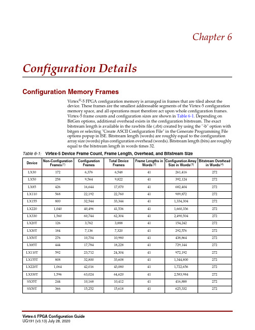
Table 6-1: Virtex-5 Device Frame Count, Frame Length, Overhead, and Bitstream Size
Device
Non-Configuration Frames (1)
Configuration Frames
Total Device Frames
Table 6-13: TIMER Register Description
Name
Bit Index
Description
TIMER_USR_MON
Watchdog is enabled during user mode:
25
0: Disabled
1: Enabled
FPGA可编程逻辑器件芯片XC2V2000-6FG456C中文规格书
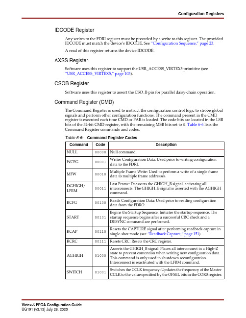
IDCODE RegisterAny writes to the FDRI register must be preceded by a write to this register. The provided IDCODE must match the device’s IDCODE. See “Configuration Sequence,” page23.A read of this register returns the device IDCODE.AXSS RegisterSoftware uses this register to support the USR_ACCESS_VIRTEX5 primitive (see“USR_ACCESS_VIRTEX5,” page103).CSOB RegisterSoftware uses this register to assert the CSO_B pin for parallel daisy-chain operation. Command Register (CMD)The Command Register is used to instruct the configuration control logic to strobe global signals and perform other configuration functions. The command present in the CMD register is executed each time CMD or FAR is loaded. The code bits are located in the LSB bits of the 32-bit CMD register, with the remaining MSB bits set to 0. Table6-6 lists the Command Register commands and codes.Table 6-6:Command Register CodesCommand Code DescriptionNULL00000Null command.WCFG00001Writes Configuration Data: Used prior to writing configuration data to the FDRI.MFW00010Multiple Frame Write: Used to perform a write of a single frame data to multiple frame addresses.DGHIGH/ LFRM 00011Last Frame: Deasserts the GHIGH_B signal, activating allinterconnects. The GHIGH_B signal is asserted with the AGHIGHcommand.RCFG00100Reads Configuration Data: Used prior to reading configuration data from the FDRO.START00101Begins the Startup Sequence: Initiates the startup sequence. The startup sequence begins after a successful CRC check and a DESYNC command are performed.RCAP00110Resets the CAPTURE signal after performing readback-capture in single-shot mode (see “Readback Capture,” page151).RCRC00111Resets CRC: Resets the CRC register.AGHIGH01000Asserts the GHIGH_B signal: Places all interconnect in a High-Z state to prevent contention when writing new configuration data. This command is only used in shutdown reconfiguration. Interconnect is reactivated with the LFRM command.SWITCH01001Switches the CCLK frequency: Updates the frequency of the Master CCLK to the value specified by the OFSEL bits in the COR0 register.Warm Boot Start Address Register (WBSTAR)The name of each bit position in the WBSTAR is given in Figure 6-6 and described in Table 6-12.DescriptionReservedPERSIST_DEASSERT_AT_DESYNCHReserved ReservedRBCRC_NO_PINRBCRC_EN ReservedBPI_1ST_READ_CYCLESBPI_PAGE_SIZEBit Index 313029282726252423222120191817161514131211109876543210ValueFigure 6-5:Configuration Options Register 1Table 6-11:Configuration Options Register 1 Description NameBit IndexDescriptionPERSIST_DEASSERT_AT_DESYNCH 17Enables deassertion of PERSIST with the DESYNCH commandRBCRC_NO_PIN 9Disables INIT_B as read back CRC error status output pinRBCRC_EN8Continuous readback CRC enable BPI_1ST_READ_CYCLES[3:2]First byte read timing:00: 1 C C LK 01: 2 C C LKs 10: 3 C C LKs 11: 4 C C LKs BPI_PAGE_SIZE [1:0]Flash memory page size:00: 1byte/word 01: 4 bytes/words 10: 8 bytes/words 11: ReservedChapter 6:Configuration DetailsWatchdogFPGA End of StartupTo use the Watchdog to monitor the bitstream configuration, set TIMER_CFG_MON to 1 and the desired TIMER_VALUE in a write to the TIMER register in the bitstream. The TIMER_VALUE should be adequate to cover the entire FPGA configuration time until startup is complete. Any wait time in startup for DCI match, DCM lock, or DONE should also be included.Once enabled, the watchdog timer starts to count down. If the timer reaches 0 and the FPGA has not reached the final state of startup, a watchdog time-out error occurs and triggers a fallback configuration.User OperationTo use the Watchdog to monitor the user logic, set TIMER_USR_MON to 1 and the desired TIMER_VALUE in a write to the TIMER register in the bitstream. The user must constantly reset the watchdog counter before it times out, either by the LTIMER command or by directly accessing the TIMER register. The watchdog is automatically disabled when the device is shut down or on power down (including shutdown).Table 8-6 shows an example bitstream for reloading the Watchdog using the LTIMER command.Table 8-7 shows an example bitstream for directly accessing the TIMER register:Table 8-6:Example Bitstream for Reloading the Watchdog with LTIMERConfiguration Data(hex)Explanation FFFFFFFF Dummy Word AA995566 Sync Word 20000000 Type 1 NO OP30008001 Type 1 Write 1 Words to CMD00000000 NULL 20000000 Type 1 NO OP30008001 Type 1 Write 1 Words to CMD00000011 LTIMER Command 20000000 Type 1 NO OP30008001 Type 1 Write 1 Words to CMD0000000D DESYNCH 20000000Type 1 NO OPTable 8-7:Example Bitstream for Accessing the TIMER RegisterConfiguration Data(hex)Explanation FFFFFFFF Dummy Word AA995566Sync WordChapter 9:Readback CRC。
FPGA可编程逻辑器件芯片XC2S200E-6FGG456C中文规格书
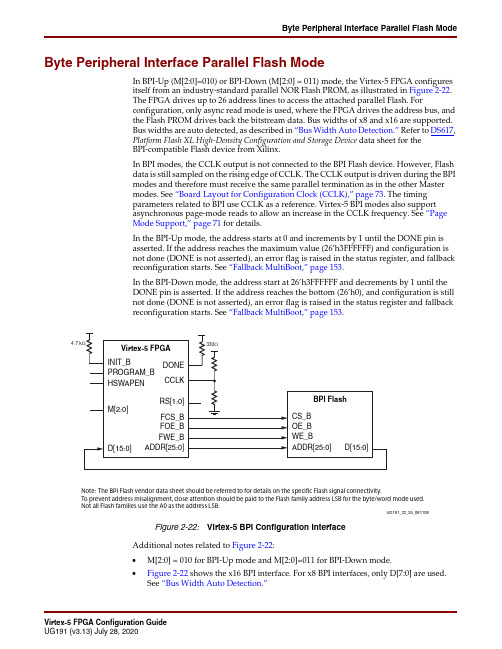
Byte Peripheral Interface Parallel Flash ModeByte Peripheral Interface Parallel Flash ModeIn BPI-Up (M[2:0]=010) or BPI-Down (M[2:0]=011) mode, the Virtex-5 FPGA configures itself from an industry-standard parallel NOR Flash PROM, as illustrated in Figure 2-22. The FPGA drives up to 26 address lines to access the attached parallel Flash. Forconfiguration, only async read mode is used, where the FPGA drives the address bus, and the Flash PROM drives back the bitstream data. Bus widths of x8 and x16 are supported. Bus widths are auto detected, as described in “Bus Width Auto Detection.” Refer to DS617, Platform Flash XL High-Density Configuration and Storage Device data sheet for the BPI-compatible Flash device from Xilinx.In BPI modes, the CCLK output is not connected to the BPI Flash device. However, Flash data is still sampled on the rising edge of CCLK. The CCLK output is driven during the BPI modes and therefore must receive the same parallel termination as in the other Master modes. See “Board Layout for Configuration Clock (CCLK),” page 73. The timing parameters related to BPI use CCLK as a reference. Virtex-5 BPI modes also support asynchronous page-mode reads to allow an increase in the CCLK frequency. See “Page Mode Support,” page 71 for details.In the BPI-Up mode, the address starts at 0 and increments by 1 until the DONE pin is asserted. If the address reaches the maximum value (26’h3FFFFFF) and configuration is not done (DONE is not asserted), an error flag is raised in the status register, and fallback reconfiguration starts. See “Fallback MultiBoot,” page 153.In the BPI-Down mode, the address start at 26’h3FFFFFF and decrements by 1 until the DONE pin is asserted. If the address reaches the bottom (26’h0), and configuration is still not done (DONE is not asserted), an error flag is raised in the status register and fallback reconfiguration starts. See “Fallback MultiBoot,” page 153.Additional notes related to Figure 2-22:∙M[2:0]=010 for BPI-Up mode and M[2:0]=011 for BPI-Down mode.∙Figure 2-22 shows the x16 BPI interface. For x8 BPI interfaces, only D[7:0] are used.See “Bus Width Auto Detection.”Figure 2-22:Virtex-5 BPI Configuration InterfaceUG191_c2_25_0611084.7 k Note: The BPI Flash vendor data sheet should be referred to for details on the specific Flash signal connectivity.To prevent address misalignment, close attention should be paid to the Flash family address LSB for the byte/word mode used. Not all Flash families use the A0 as the address LSB.Board Layout for Configuration Clock (CCLK)Chapter 2:Configuration InterfacesBoundary-Scan for Virtex-5 Devices Using IEEE Standard 1149.1Single Device ConfigurationTable3-4 describes the TAP controller commands required to configure a Virtex-5 device.Refer to Figure3-2 for TAP controller states. These TAP controller commands are issuedautomatically if configuring the part with the iMPACT software.Table 3-4: Single Device Configuration SequenceTAP Controller Step and Description Set and Hold# of Clocks TDI TMS TCK1.On power-up, place a logic 1 on the TMS, and clockthe TCK five times. This ensures starting in the TLR(Test-Logic-Reset) state.X152.Move into the RTI state.X013.Move into the SELECT-IR state.X124.Enter the SHIFT-IR state.X025.Start loading the CFG_IN instruction, LSB first:111000101096.Load the MSB of CFG_IN instruction when exitingSHIFT-IR, as defined in the IEEE standard.1117.Enter the SELECT-DR state.X128.Enter the SHIFT-DR state.X029.Shift in the Virtex-5 bitstream. Bitn (MSB) is the firstbit in the bitstream(1).bit1...bit n0(bits in bitstream)-110.Shift in the last bit of the bitstream. Bit0 (LSB) shiftson the transition to EXIT1-DR.bit01111.Enter UPDATE-DR state.X1112.Reset TAP by clocking five 1s on TMS X1513.Move into RTI state.X0114.Enter the SELECT-IR state.X1215.Move to the SHIFT-IR state.X0216.Start loading the JSTART instruction. The JSTARTinstruction initializes the startup sequence.1110011000917.Load the last bit of the JSTART instruction.11118.Move to the UPDATE-IR state.X1119.Move to the RTI state and clock the startupsequence by applying a minimum of 12 clock cyclesto the TCK.X01220.Move to the TLR state. The device is now functional.X13Notes:1.In the Configuration Register, data is shifted in from the right (TDI) to the left (TDO), MSB first. (Shifts into the Configuration Register aredifferent from shifts into the other registers in that they are MSB first.)Chapter 4:User PrimitivesCAPTURE_VIRTEX5The CAPTURE_VIRTEX5 primitive is used to capture I/O, CLB, and block RAM outputflip-flop status, and then read back through the configuration interface. The CAP input issampled by CLK to generate an internal gcap signal. The I/O and CLB flip-flop status arecaptured into an FPGA configuration memory cell when the gcap signal is High. There areoperation modes, a one-shot mode, or a continuous mode.In one-shot mode, after the first CAP falling edge, gcap is held to 0 to avoid furthercapturing. An explicit RCAP command is required to re-arm the capture circuit.In continuous mode, the CAP input is simply sampled by CLK, and becomes the gcapsignal, allowing the user to control when to capture.CAPTURE_VIRTEX5 should not operate simultaneously with the FRAME_ECC_VIRTEX5primitive or the Readback CRC function (see Chapter9, “Readback CRC”) becausecapturing a value into configuration memory might cause a false error.Table 4-2:CAPTURE_VIRTEX5 Pin TablePin Name Type DescriptionCLK Input Clock for sampling the CAP input.CAP Input Active-High capture enable. The CAP input is sampled bythe rising edge of CLK.ICAP_VIRTEX5The ICAP_VIRTEX5 primitive works the same way as the SelectMAP configurationinterface except it is on the fabric side, and ICAP has a separate read/write bus, as opposedto the bidirectional bus in SelectMAP. The general SelectMAP timing diagrams and theSelectMAP bitstream ordering information as described in the “SelectMAP ConfigurationInterface” section of this user guide are also applicable to ICAP. It allows the user to accessconfiguration registers, readback configuration data, or partially reconfigure the FPGAafter configuration is done.ICAP has three data width selections through the ICAP WIDTH parameter: x8, x16, andx32.The two ICAP ports cannot be operated simultaneously. The design must start from the topICAP, then switch back and forth between the two.Table 4-3:ICAP_VIRTEX5 Pin TablePin Name Type DescriptionCLK Input ICAP interface clockCE Input Active-Low ICAP interface select. Equivalent to CS_B inthe SelectMAP interface.WRITE Input0=WRITE, 1=READ. Equivalent to the RDWR_B signal inthe SelectMAP interface.I[31:0]Input ICAP write data bus. The bus width depends onICAP_WIDTH parameter. The bit ordering is identical tothe SelectMAP interface. See SelectMap Data Ordering inFigure2-19.。
FPGA可编程逻辑器件芯片XC2V500-5FGG456I中文规格书
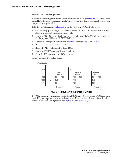
Chapter 3:Boundary-Scan and JTAG ConfigurationMultiple Device ConfigurationIt is possible to configure multiple Virtex-5 devices in a chain. (See Figure3-7.) The devicesin the JTAG chain are configured one at a time. The multiple device configuration steps canbe applied to any size chain.Refer to the state diagram in Figure3-2 for the following TAP controller steps:1.On power-up, place a logic 1 on the TMS and clock the TCK five times. This ensuresstarting in the TLR (Test-Logic-Reset) state.2.Load the CFG_IN instruction into the target device (and BYPASS in all other devices).Go through the RTI state (RUN-TEST/IDLE).3.Load in the configuration bitstream per step7 through step11 in Table3-4.4.Repeat step2 and step3 for each device.5.Reset all TAPs by clocking five 1s on TMS.6.Load the JSTART command into all devices.7.Go to the RTI state and clock TCK 12 times.All devices are active at this point.JT AG He a derDevice 0Device 1Device 2UG191_c3_01_020609Figure 3-7:Boundary-Scan Chain of DevicesIf JTAG is the only configuration mode, then PROGRAM_B, INIT_B, and DONE can eachbe tied High to separate resistors as shown in the Master serial or Master/Slave SerialMode Daisy Chain Configuration (see Figure2-3 and Figure2-4).Boundary-Scan for Virtex-5 Devices Using IEEE Standard 1149.1Reconfiguring through Boundary-ScanThe ability of Virtex-5 devices to perform partial reconfiguration is the reason that the configuration memory is not cleared when reconfiguring the device. When reconfiguring a chain of devices, refer to step3 in Table3-4. There are two methods to reconfigure Virtex-5 devices without possible internal contention. The first method is to pulse thePROGRAM_B pin, resetting the internal configuration memory. The alternate method is to perform a shutdown sequence, placing the device in a safe state. The following shutdown sequence includes using internal registers. (For details on internal registers, refer toChapter7, “Readback and Configuration Verification.”)1.Load the CFG_IN instruction.2.In the SHIFT-DR state, load the synchronization word followed by the Reset CRCRegister (RCRC) command.1111 1111 1111 1111 1111 1111 1111 1111∅ Dummy word1010 1010 1001 1001 0101 0101 0110 0110∅ Synchronization word0011 0000 0000 0000 1000 0000 0000 0001∅ Header: Write to CMD register0000 0000 0000 0000 0000 0000 0000 0111∅ RCRC command0010 0000 0000 0000 0000 0000 0000 0000∅ NO-OP0000 0000 0000 0000 0000 0000 0000 0000∅ flush pipe3.Load JSHUTDOWN.4.Go to the RTI state and clock TCK at least 12 times to clock the shutdown sequence.5.Proceed to the SHIFT-IR state and load the CFG_IN instruction again.6.Go to the SHIFT-DR state and load the configuration bits. Make sure the configurationbits contain the AGHIGH command, asserting the global signal GHIGH_B. Thisprevents contention while writing configuration data.0011 0000 0000 0000 1000 0000 0000 0001∅ Header: Write to CMD0000 0000 0000 0000 0000 0000 0000 1000∅ AGHIGH command assertsGHIGH_B0000 0000 0000 0000 0000 0000 0000 0000∅ flush pipe7.When all configuration bits have been loaded, reset the TAP by clocking five 1s onTMS.8.Go to the SHIFT-IR state and load the JSTART instruction.9.Go to the RTI state and clock TCK at least 12 times to clock the startup sequence.10.Go to the TLR state to complete the reconfiguration process.Chapter 3:Boundary-Scan and JTAG ConfigurationChapter 5:Dynamic Reconfiguration Port (DRP)Configuration RegistersTable 6-9:Status Register DescriptionName Bit Index DescriptionBUS_WIDTH[26:25]CFG bus width auto detection result. If ICAP is enabled,this field reflects the ICAP bus width afterconfiguration is done.00 = x101 = x810 = x1611 = x32FS[24:22]SPI Flash type selectSTARTUP_STATE[20:18]CFG startup state machine (0 to 7).Phase 0 = 000Phase 1 = 001Phase 2 = 011Phase 3 = 010Phase 4 = 110Phase 5 = 111Phase 6 = 101Phase 7 = 100DEC_ERROR16FDRI write attempted before or after decrypt operation: 0:No DEC_ERROR1:DEC_ERRORID_ERROR15Attempt to write to FDRI without successful DEVICE_ID check.0:No ID_ERROR1:ID_ERRORDONE14Value on DONE pinRELEASE_DONE13Value of internal DONE signal:0:DONE signal not released (pin is actively held Low) 1:DONE signal released (can be held Low externally)INIT_B12Value on INIT_B pinINIT_COMPLETE11Internal signal indicating initialization has completed: 0:Initialization has not finished1:Initialization finishedMODE[10:8]Status of the Mode pins (M[2:0]).GHIGH_B7Status of GHIGH_B:0:GHIGH_B asserted 1:GHIGH_B deassertedGWE6Status of GWE:0:FFs and block RAM are write disabled 1:FFs and block RAM are write enabled。
FPGA可编程逻辑器件芯片XC2V1000-4FGG456C中文规格书
Linux Device DriverThe Linux device driver has the following character device interfaces:•User character device for access to user components.•Control character device for controlling DMA/Bridge Subsystem for PCI Express®components.•Events character device for waiting for interrupt events.•SGDMA character devices for high performance transfers.The user accessible devices are as follows:•XDMA0_control: Used to access DMA/Bridge Subsystem for PCI Express® registers.•XDMA0_user: Used to access AXI-Lite master interface.•XDMA0_bypass: Used to access DMA Bypass interface.•XDMA0_events_*: Used to recognize user interrupts.Using the DriverThe XDMA drivers can be downloaded from the Xilinx DMA IP Drivers page.Interrupt ProcessingLegacy InterruptsThere are four types of legacy interrupts: A, B, C and D. You can select any interrupts in the PCIe Misc tab under Legacy Interrupt Settings. You must program the corresponding values for both the IRQ Block Channel Vector (see IRQ Block Channel Vector Number (0xA0)) and the IRQ Block User Vector (see IRQ Block User Vector Number (0x80)). Values for each legacy interrupts are A = 0, B = 1, C = 2 and D = 3. The host recognizes interrupts only based on these values.MSI InterruptsFor MSI interrupts, you can select from 1 to 32 vectors in the PCIe Misc tab under MSICapabilities, which consists of a maximum of 16 usable DMA interrupt vectors and a maximum of16 usable user interrupt vectors. The Linux operating system (OS) supports only 1 vector. Otheroperating systems might support more vectors and you can program different vectors values in the IRQ Block Channel Vector (see IRQ Block Channel Vector Number (0xA0)) and in the IRQBlock User Vector (see IRQ Block User Vector Number (0x80)) to represent different interruptsources. The Xilinx® Linux driver supports only 1 MSI vector.MSI-X InterruptsThe DMA supports up to 32 different interrupt source for MSI-X, which consists of a maximum of 16 usable DMA interrupt vectors and a maximum of 16 usable user interrupt vectors. TheDMA has 32 MSI-X tables, one for each source (see MSI-X Vector Table and PBA (0x00–0xFE0)).For MSI-X channel interrupt processing the driver should use the Engine’s Interrupt Enable Mask for H2C and C2H (see H2C Channel Interrupt Enable Mask (0x90) or Table C2H ChannelInterrupt Enable Mask (0x90)) to disable and enable interrupts.User InterruptsThe user logic must hold usr_irq_req active-High even after receiving usr_irq_ack (acks) to keep the interrupt pending register asserted. This enables the Interrupt Service Routine (ISR) within the driver to determine the source of the interrupt. Once the driver receives userinterrupts, the driver or software can reset the user interrupts source to which hardware should respond by deasserting usr_irq_req.Example H2C FlowIn the example H2C flow,loaddriver.sh loads devices for all available channels. Thedma_to_device user program transfers data from host to Card.The example H2C flow sequence is as follows:1.Open the H2C device and initialize the DMA.2.The user program reads the data file, allocates a buffer pointer, and passes the pointer towrite function with the specific device (H2C) and data size.3.The driver creates a descriptor based on input data/size and initializes the DMA withdescriptor start address, and if there are any adjacent descriptor.4.The driver writes a control register to start the DMA transfer.Appendix A: Application Software Development5.The DMA reads descriptor from the host and starts processing each descriptor.6.The DMA fetches data from the host and sends the data to the user side. After all data istransferred based on the settings, the DMA generates an interrupt to the host.7.The ISR driver processes the interrupt to find out which engine is sending the interrupt andchecks the status to see if there are any errors. It also checks how many descriptors areprocessed.8.After the status is good, the drive returns transfer byte length to user side so it can check forthe same.Example C2H FlowIn the example C2H flow,loaddriver.sh loads the devices for all available channels. Thedma_from_device user program transfers data from Card to host.The example C2H flow sequence is as follow:1.Open device C2H and initialize the DMA.2.The user program allocates buffer pointer (based on size), passes pointer to read functionwith specific device (C2H) and data size.3.The driver creates descriptor based on size and initializes the DMA with descriptor startaddress. Also if there are any adjacent descriptor.4.The driver writes control register to start the DMA transfer.5.The DMA reads descriptor from host and starts processing each descriptor.6.The DMA fetches data from Card and sends data to host. After all data is transferred basedon the settings, the DMA generates an interrupt to host.7.The ISR driver processes the interrupt to find out which engine is sending the interrupt andchecks the status to see if there are any errors and also checks how many descriptors areprocessed.8.After the status is good, the drive returns transfer byte length to user side so it can check forthe same.。
FPGA可编程逻辑器件芯片XC2V250-6FG456C中文规格书

Generating PROM Files in x16 mode. The FPGA now knows on which bus width to receive the rest of the data. Nopacket processed by the FPGA until the Sync word is found. See Table5-7.Table 5-7:Sync Word31:2423:1615:87:00xAA0x990x550x66Generating PROM FilesPROM files are generated from bitstream files with the PROMGen utility. Users can accessPROMGen directly from the command line or indirectly through the iMPACT FileGeneration Mode. For PROMGen syntax, refer to UG628, Command Line Tools User Guide.For information on iMPACT software, refer to the ISE® software documentation. PROMfiles serve to reformat bitstream files for PROM programming and combine bitstream filesfor serial daisy-chains (see PROM Files for Serial Daisy-Chains).PROM Files for Serial Daisy-ChainsConfiguration data for serial daisy-chains requires special formatting because separateBIT files cannot simply be concatenated together to program the daisy-chain. The specialformatting is performed by PROMGen (or iMPACT software) when generating a PROMfile from multiple bitstreams. To generate the PROM file, specify multiple bitstreams usingthe PROMGen -n, -u, and -d options or the iMPACT Software File Generation Wizard.Refer to ISE software documentation for details.PROMGen reformats the configuration bitstreams by nesting downstream configurationdata into configuration packets for upstream devices. Attempting to program the chain bysending multiple bitstreams to the first device causes the first device to configure and thenignore the subsequent data.PROM Files for SelectMAP ConfigurationThe MCS file format is most commonly used to program Xilinx® configuration PROMsthat in turn program a single FPGA in SelectMAP mode. For custom configurationsolutions, the BIN and HEX files are the easiest PROM file formats to use due to their rawdata format. In some cases, additional formatting is required; refer to XAPP502, Using aMicroprocessor to Configure Xilinx FPGAs via Slave Serial or SelectMAP Mode for details.If multiple configuration bitstreams for a SelectMAP configuration reside on a singlememory device, the bitstreams must not be combined into a serial daisy-chain PROM file.Instead, the target memory device should be programmed with multiple BIN or HEX files.If a single PROM file with multiple, separate data streams is needed, one can be generatedin iMPACT software by targeting a Parallel PROM, then selecting the appropriate numberof data streams. This can also be accomplished through the PROMGen command line.Refer to PROMGen software documentation for details.PROM Files for SPI/BPI ConfigurationThe -d, -u, -spi, -s, and -data_width options in PROMGen or the iMPACT SoftwareFile Generation Wizard are used to create PROM files for third-party flash devices. Theoutput format supported by the third-party programmer is important. Some BPI devicesrequire endian-swapping to be enabled when programming the PROM file. Refer to theflash vendor's documentation.Chapter 5:Configuration DetailsControl Register 0 (CTL)The CTL register is used to configure the Spartan-6 device. Writes to the CTL register aremasked by the value in the MASK register. The name of each bit position in the CTL0register is given in Table 5-34.Caution!PERSIST and ICAP cannot be set at the same time. PERSIST has higher priority.Table 5-34:Control Register 0 (CTL0) Description Name Bit IndexDescription BitGen Default DEC 6Decryption0: No decryption1: Decryption used (automatically set SBITS to Level1 or upand mc_enc=1)Once set to 1, the DEC cannot be altered except by hardreboot (PROGRAM_B or JPROGRAM).0SBITS 5:4Security level:Level0: SBITS=00: R/W OK (default)Level1: SBITS=01: Permits only ICAP readbackLevel2: SBITS=10: All readback disabled;(en_vrb_b =1 => Vrd=0)Level3: SBITS=11: Readback disabled, Writing disabledexcept CRC,CMD; (mc_vrd=1 => Vrd=0)Once set to 1, the SBITS cannot be altered except by softreboot (PROGRAM_B, JPROGRAM, IPROG command,error reboot, or fallback reboot).00PERSIST 3Configuration interface remains after configuration0: No (default)1: Yes0USE_EFUSE_KEY 2Use eFUSE key as decryption key0: Use battery-backed RAM key (default)1: Use eFUSE key0CRC_EXTSTAT_DISABLE 1External CRC status pin (INIT_B) pulled Low when usingPOST CRC.The first configuration always has the CRC indicator onINIT_B.0: CRC indicator enabled1: CRC indicator disabledRESERVED 0Reserved.1Chapter6 Readback and Configuration VerificationSpartan®-6 devices allow users to read configuration memory through the SelectMAP,ICAP, and JTAG interfaces. During readback, the user reads all configuration memorycells, including the current values on all user memory elements (LUT RAM, SRL16, andblock RAM).To read configuration memory, users must send a sequence of commands to the device toinitiate the readback procedure. Once initiated, the device dumps the contents of itsconfiguration memory to the SelectMAP or JTAG interface. The Accessing ConfigurationRegisters through the SelectMAP Interface section and IEEE Std 1149.1 JTAG describe thesteps for reading configuration memory.Users can send the readback command sequence from a custom microprocessor, CPLD, orFPGA-based system, or use iMPACT to perform JTAG-based readback verify. iMPACT, thedevice programming software provided with the ISE® software by Xilinx, can perform allreadback and comparison functions for Spartan-6 devices and report to the user whetherthere were any configuration errors.Once configuration memory is read from the device, the next step is to determine if thereare any errors by comparing the readback bitstream to the configuration bitstream. TheVerifying Readback Data section explains how this is done.Preparing a Design for ReadbackThere are two mandatory bitstream settings for readback using JTAG or SelectMAP: theBitGen security setting must not prohibit readback (-g Security:none), and bitstreamencryption must not be used. Additionally, if readback is to be performed through theSelectMAP interface, the port must be set to retain its function after configuration bysetting the persist option in BitGen (-g Persist:Yes), otherwise the SelectMAP data pinsrevert to user I/O, precluding further configuration operations. Beyond these security andencryption requirements, no special considerations are necessary to enable readbackthrough the boundary-scan port. Also, these requirements are not necessary when usingreadback via the ICAP. Limitations for readback are:•Performing a readback while the design is in operation (without providing ashutdown command) results in reading back invalid block RAM data. The actualcontents of the block RAM are unaffected.•Performing a readback (with or without a shutdown command) corrupts the contentsof block RAMs configured in 9K mode.Chapter 6:Readback and Configuration VerificationChapter 8:Readback CRC。
FPGA可编程逻辑器件芯片XC2V500-4FGG456I中文规格书
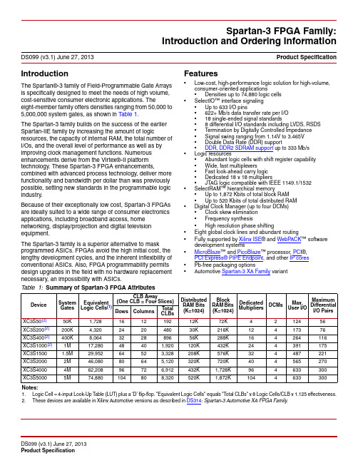
IntroductionThe Spartan®-3 family of Field-Programmable Gate Arrays is specifically designed to meet the needs of high volume, cost-sensitive consumer electronic applications. Theeight-member family offers densities ranging from 50,000 to 5,000,000 system gates, as shown in Table1.The Spartan-3 family builds on the success of the earlier Spartan-IIE family by increasing the amount of logic resources, the capacity of internal RAM, the total number of I/Os, and the overall level of performance as well as by improving clock management functions. Numerous enhancements derive from the Virtex®-II platform technology. These Spartan-3 FPGA enhancements, combined with advanced process technology, deliver more functionality and bandwidth per dollar than was previously possible, setting new standards in the programmable logic industry.Because of their exceptionally low cost, Spartan-3 FPGAs are ideally suited to a wide range of consumer electronics applications, including broadband access, home networking, display/projection and digital television equipment.The Spartan-3 family is a superior alternative to mask programmed ASICs. FPGAs avoid the high initial cost, the lengthy development cycles, and the inherent inflexibility of conventional ASICs. Also, FPGA programmability permits design upgrades in the field with no hardware replacement necessary, an impossibility with ASICs.Features•Low-cost, high-performance logic solution for high-volume, consumer-oriented applications•Densities up to 74,880 logic cells•SelectIO™ interface signaling•Up to 633 I/O pins•622+ Mb/s data transfer rate per I/O•18 single-ended signal standards•8 differential I/O standards including LVDS, RSDS•Termination by Digitally Controlled Impedance•Signal swing ranging from 1.14V to 3.465V•Double Data Rate (DDR) support•DDR, DDR2 SDRAM support up to 333Mb/s•Logic resources•Abundant logic cells with shift register capability•Wide, fast multiplexers•Fast look-ahead carry logic•Dedicated 18 x 18 multipliers•JT AG logic compatible with IEEE 1149.1/1532•SelectRAM™ hierarchical memory•Up to 1,872 Kbits of total block RAM•Up to 520 Kbits of total distributed RAM•Digital Clock Manager (up to four DCMs)•Clock skew elimination•Frequency synthesis•High resolution phase shifting•Eight global clock lines and abundant routing•Fully supported by Xilinx ISE® and WebP ACK™ software development systems•MicroBlaze™ and PicoBlaze™ processor, PCI®,PCI Express® PIPE Endpoint, and other IP cores•Pb-free packaging options•Automotive Spartan-3 XA Family variantSpartan-3 FPGA Family:Introduction and Ordering Information DS099 (v3.1) June 27, 2013Product SpecificationTable 1:Summary of Spartan-3 FPGA AttributesDevice SystemGatesEquivalentLogic Cells(1)CLB Array(One CLB = Four Slices)DistributedRAM Bits(K=1024)BlockRAM Bits(K=1024)DedicatedMultipliers DCMsMax.User I/OMaximumDifferentialI/O Pairs Rows Columns TotalCLBsXC3S50(2)50K1,728161219212K72K4212456XC3S200(2)200K4,320242048030K216K12417376XC3S400(2)400K8,064322889656K288K164264116XC3S1000(2)1M17,28048401,920120K432K244391175XC3S1500 1.5M29,95264523,328208K576K324487221XC3S20002M46,08080645,120320K720K404565270XC3S40004M62,20896726,912432K1,728K964633300XC3S50005M74,880104808,320520K1,872K1044633300Notes:1.Logic Cell = 4-input Look-Up T able (LUT) plus a ‘D’ flip-flop. "Equivalent Logic Cells" equals "T otal CLBs" x 8 Logic Cells/CLB x 1.125 effectiveness.2.These devices are available in Xilinx Automotive versions as described in DS314: Spartan-3 Automotive XA FPGA Family.Differential standards employ a pair of signals, one the opposite polarity of the other. The noise canceling (e.g., Common-Mode Rejection) properties of these standards permit exceptionally high data transfer rates. This section introduces the differential signaling capabilities of Spartan-3 devices.Each device-package combination designates specific I/O pairs that are specially optimized to support differentialstandards. A unique “L-number”, part of the pin name, identifies the line-pairs associated with each bank (see Figure 40, page 112). For each pair, the letters ‘P’ and ‘N’ designate the true and inverted lines, respectively. For example, the pin names IO_L43P_7 and IO_L43N_7 indicate the true and inverted lines comprising the line pair L43 on Bank 7. The V CCO lines provide current to the outputs. The V CCAUX lines supply power to the differential inputs, making them independent of the V CCO voltage for an I/O bank. The V REF lines are not used. Select the V CCO level to suit the desired differential standard according to Table 9.Table 8:Single-Ended I/O StandardsSignal Standard (IOSTANDARD)V CCO (Volts)V REF for Inputs(Volts)(1)Board Termination Voltage (V TT ) in VoltsFor Outputs For Inputs GTL Note 2Note 20.8 1.2GTLP Note 2Note 21 1.5HSTL_I 1.5–0.750.75HSTL_III 1.5–0.9 1.5HSTL_I_18 1.8–0.90.9HSTL_II_18 1.8–0.90.9HSTL_III_18 1.8– 1.1 1.8LVCMOS12 1.2 1.2––LVCMOS15 1.5 1.5––LVCMOS18 1.8 1.8––LVCMOS25 2.5 2.5––LVCMOS33 3.3 3.3––LVTTL 3.3 3.3––PCI33_3 3.0 3.0––SSTL18_I 1.8–0.90.9SSTL18_II 1.8–0.90.9SSTL2_I 2.5– 1.25 1.25SSTL2_II 2.5–1.251.25Notes:1.Banks 4 and 5 of any Spartan-3 device in a VQ100 package do not support signal standards using V REF .2.The V CCO level used for the GTL and GTLP standards must be no lower than the termination voltage (V TT ), nor can it be lower than the voltage at the I/O pad.3.See Table 10 for a listing of the single-ended DCI standards.Spartan-3 FPGA Family: DC and Switching CharacteristicsTable 67:Timing for the Master and Slave Parallel Configuration ModesSymbol Description Slave/MasterAll Speed GradesUnitsMin MaxClock-to-Output TimesT SMCKBY The time from the rising transition on the CCLK pin to a signal transition atthe BUSY pinSlave–12.0nsSetup TimesT SMDCC The time from the setup of data at the D0-D7 pins to the rising transition atthe CCLK pinBoth10.0–nsT SMCSCC The time from the setup of a logic level at the CS_B pin to the risingtransition at the CCLK pin10.0–nsT SMCCW(3)The time from the setup of a logic level at the RDWR_B pin to the risingtransition at the CCLK pin10.0–ns Hold TimesT SMCCD The time from the rising transition at the CCLK pin to the point when datais last held at the D0-D7 pinsBoth0–nsT SMCCCS The time from the rising transition at the CCLK pin to the point when a logiclevel is last held at the CS_B pin0–nsT SMWCC(3)The time from the rising transition at the CCLK pin to the point when a logiclevel is last held at the RDWR_B pin0–ns。
FPGA可编程逻辑器件芯片XC2V4000-5FG456C中文规格书
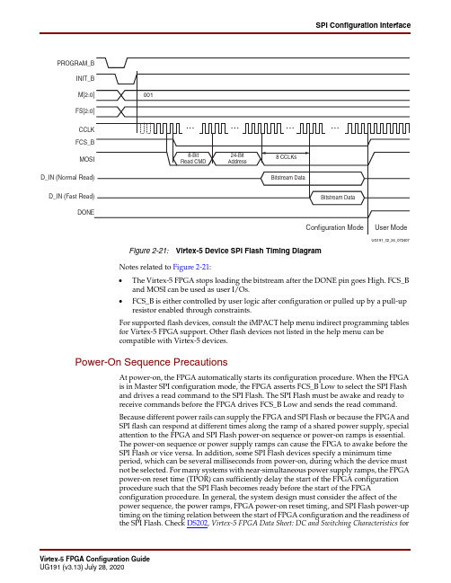
SPI Configuration InterfaceNotes related to Figure 2-21:∙The Virtex-5 FPGA stops loading the bitstream after the DONE pin goes High. FCS_B and MOSI can be used as user I/Os.∙FCS_B is either controlled by user logic after configuration or pulled up by a pull-up resistor enabled through constraints.For supported flash devices, consult the iMPACT help menu indirect programming tables for Virtex-5FPGA support. Other flash devices not listed in the help menu can be compatible with Virtex-5devices.Power-On Sequence PrecautionsAt power-on, the FPGA automatically starts its configuration procedure. When the FPGA is in Master SPI configuration mode, the FPGA asserts FCS_B Low to select the SPI Flash and drives a read command to the SPI Flash. The SPI Flash must be awake and ready to receive commands before the FPGA drives FCS_B Low and sends the read command.Because different power rails can supply the FPGA and SPI Flash or because the FPGA and SPI flash can respond at different times along the ramp of a shared power supply, special attention to the FPGA and SPI Flash power-on sequence or power-on ramps is essential. The power-on sequence or power supply ramps can cause the FPGA to awake before the SPI Flash or vice versa. In addition, some SPI Flash devices specify a minimum timeperiod, which can be several milliseconds from power-on, during which the device must not be selected. For many systems with near-simultaneous power supply ramps, the FPGA power-on reset time (TPOR) can sufficiently delay the start of the FPGA configuration procedure such that the SPI Flash becomes ready before the start of the FPGAconfiguration procedure. In general, the system design must consider the affect of the power sequence, the power ramps, FPGA power-on reset timing, and SPI Flash power-up timing on the timing relation between the start of FPGA configuration and the readiness of the SPI Flash. Check DS202, Virtex-5 FPGA Data Sheet: DC and Switching Characteristics forFigure 2-21:Virtex-5 Device SPI Flash Timing DiagramPROGRAM_BF S FC S MO D_IN (Norm a l Re a D_IN (F as t Re a UG191_c2_24_072407Board Layout for Configuration Clock (CCLK)Chapter 2:Configuration InterfacesBoundary-Scan for Virtex-5 Devices Using IEEE Standard 1149.1Figure 3-4 shows the instruction capture values loaded into the IR as part of an instruction scan sequence.Table 3-3:Virtex-5 Device Boundary-Scan InstructionsBoundary-Scan Command Binary Code[9:0]DescriptionEXTEST 1111000000Enables Boundary-Scan EXTEST operation.SAMPLE 1111000001Enables Boundary-Scan SAMPLE ER11111000010Access user-defined register ER21111000011Access user-defined register ER31111100010Access user-defined register ER41111100011Access user-defined register 4.CFG_OUT 1111000100Access the configuration bus for readback.CFG_IN 1111000101Access the configuration bus for configuration.INTEST 1111000111Enables Boundary-Scan INTEST ERCODE 1111001000Enables shifting out user code.IDCODE 1111001001Enables shifting out of ID code.HIGHZ 11110010103-state output pins while enabling BYPASS Register.JPROGRAM 1111001011Equivalent to and has the same effect as PROGRAM.JSTART 1111001100Clocks the startup sequence when StartClk is TCK.JSHUTDOWN 1111001101Clocks the shutdown sequence.SYSMON 1111110111System Monitor DRP access through JTAG. See the DRP interface section in UG192: Virtex-5 FPGA System Monitor User Guide.ISC_ENABLE 1111010000Marks the beginning of ISC configuration. Full shutdown is executed.ISC_PROGRAM 1111010001Enables in-system programming.ISC_PROGRAM_KEY 1111010010Change security status from secure to non-secure mode and vice versa.ISC_NOOP 1111010100No operation.ISC_READ 1111010101Used to read back the device configuration data per IEEE std 1532 and the Battery-backed RAM (BBR). The BBR holds the encryption key for the AES bitstream encryption.ISC_DISABLE 1111010111Completes ISC configuration. Startup sequence is executed.BYPASS 1111111111Enables BYPASS.RESERVEDAll other codesXilinx reserved instructions.Chapter 3:Boundary-Scan and JTAG ConfigurationBYPASS RegisterThe other standard data register is the single flip-flop BYPASS register. It passes data serially from the TDI pin to the TDO pin during a bypass instruction. This register is initialized to zero when the TAP controller is in the CAPTURE-DR state.Identification (IDCODE) RegisterVirtex devices have a 32-bit identification register called the IDCODE register. TheIDCODE is based on the IEEE 1149.1 standard, and is a fixed, vendor-assigned value that is used to identify electrically the manufacturer and the type of device that is beingaddressed. This register allows easy identification of the part being tested or programmed by Boundary-Scan, and it can be shifted out for examination by using the IDCODE instruction.The last bit of the IDCODE is always 1 (based on JTAG IEEE 1149.1). The last three hex digits appear as 0x093. IDCODEs assigned to Virtex-5 FPGAs are shown in Table 1-13, page 29.JTAG Configuration RegisterThe JTAG Configuration register is a 32-bit register. This register allows access to the configuration bus and readback operations.USERCODE RegisterThe USERCODE instruction is supported in the Virtex-5 family. This register allows a user to specify a design-specific identification code. The USERCODE can be programmed into the device and can be read back for verification later. The USERCODE is embedded into the bitstream during bitstream generation (BitGen -g UserID option) and is valid only after configuration. If the device is blank or the USERCODE was not programmed, the USERCODE register contains 0xFFFFFFFF .USER1, USER2, USER3, and USER4 RegistersThe USER1, USER2, USER3, and USER4 registers are only available after configuration. These four registers must be defined by the user within the design. These registers can be accessed after they are defined by the TAP pins.The BSCAN_VIRTEX5 library macro is required when creating these registers. This symbol is only required for driving internal scan chains (USER1, USER2, USER3, and USER4). A common input pin (TDI) and shared output pins represent the state of the TAP controller (RESET, SHIFT, and UPDATE). Virtex-5 TAP pins are dedicated and do not require the BSCAN_VIRTEX5 macro for normal Boundary-Scan instructions or operations. For HDL, the BSCAN_VIRTEX5 macro must be instantiated in the design.TDI ∅IR[9:6]IR[5]IR[4]IR[3]IR[2]IR[1:0]∅TDOReservedDONEINIT (1)ISC_ENABLEDISC_DONE0 1Notes:1.INIT is the status bit of the INIT_COMPLETE signal.Figure 3-4:Virtex-5 Device Instruction Capture Values Loaded into IR as Part of an Instruction ScanSequence。
FPGA可编程逻辑器件芯片XC2V80-5FG456I中文规格书

Byte Peripheral Interface Parallel Flash ModeByte Peripheral Interface Parallel Flash ModeIn BPI-Up (M[2:0]=010) or BPI-Down (M[2:0]=011) mode, the Virtex-5 FPGA configuresitself from an industry-standard parallel NOR Flash PROM, as illustrated in Figure 2-22.The FPGA drives up to 26 address lines to access the attached parallel Flash. Forconfiguration, only async read mode is used, where the FPGA drives the address bus, andthe Flash PROM drives back the bitstream data. Bus widths of x8 and x16 are supported.Bus widths are auto detected, as described in “Bus Width Auto Detection.” Refer to DS617,Platform Flash XL High-Density Configuration and Storage Device data sheet for theBPI-compatible Flash device from Xilinx.In BPI modes, the CCLK output is not connected to the BPI Flash device. However, Flashdata is still sampled on the rising edge of CCLK. The CCLK output is driven during the BPImodes and therefore must receive the same parallel termination as in the other Mastermodes. See “Board Layout for Configuration Clock (CCLK),” page 73. The timingparameters related to BPI use CCLK as a reference. Virtex-5 BPI modes also supportasynchronous page-mode reads to allow an increase in the CCLK frequency. See “PageMode Support,” page 71 for details.In the BPI-Up mode, the address starts at 0 and increments by 1 until the DONE pin isasserted. If the address reaches the maximum value (26’h3FFFFFF) and configuration isnot done (DONE is not asserted), an error flag is raised in the status register, and fallbackreconfiguration starts. See “Fallback MultiBoot,” page 153.In the BPI-Down mode, the address start at 26’h3FFFFFF and decrements by 1 until theDONE pin is asserted. If the address reaches the bottom (26’h0), and configuration is stillnot done (DONE is not asserted), an error flag is raised in the status register and fallbackreconfiguration starts. See “Fallback MultiBoot,” page 153.Additional notes related to Figure 2-22:∙M[2:0]=010 for BPI-Up mode and M[2:0]=011 for BPI-Down mode.∙Figure 2-22 shows the x16 BPI interface. For x8 BPI interfaces, only D[7:0] are used.See “Bus Width Auto Detection.”Figure 2-22:Virtex-5 BPI Configuration InterfaceUG191_c2_25_0611084.7 k Note: The BPI Flash vendor data sheet should be referred to for details on the specific Flash signal connectivity.To prevent address misalignment, close attention should be paid to the Flash family address LSB for the byte/word mode used.Not all Flash families use the A0 as the address LSB.Chapter 2:Configuration Interfaces∙Sending a bitstream to the data pin follows the same bit-swapping rule as in SelectMAP mode. See “Parallel Bus Bit Order.”∙If Flash programming is not required, FCS_B, FOE_B, and FWE_B can be tied off; that is, DONE is connected to FCS_B, FOE_B is tied Low, and FWE_B is tied High.∙The CCLK outputs are not used to connect to Flash but are used to sample Flash readdata during configuration. All timings are referenced to CCLK. The CCLK pin mustnot be driven or tied High or Low.∙The RS[1:0] pins are not connected as shown in Figure 2-22. These output pins areonly required for MultiBoot configuration. See Chapter 8, “Reconfiguration andMultiBoot.”∙HSWAPEN must be connected to either disable or enable the pull-up resistors.∙If HSWAPEN is left unconnected or tied High, a pull-up resistor is required forFCS_B.∙If HSWAPEN is tied Low, the FCB_B, FOE_B, FWE_B, and the address pins haveinternal weak pull-up resistors during configuration. After configuration, FCS_B canbe either controlled by I/O in user mode or by enabling a weak pull-up resistorthrough constraints.∙To enable the active driver on DONE, the DriveDONE option in BitGen must beenabled.∙“MultiBoot Bitstream Spacing,” page 155 provides information on when DCI or DCMlock wait is turned on.∙For daisy chaining FPGAs in BPI mode, see Figure 2-12, page 52.∙The BPI Flash vendor data sheet should be referred to for details on the specific Flashsignal connectivity. To prevent address misalignment, close attention should be paidto the Flash family address LSB for the byte/word mode used. Not all Flash familiesuse the A0 as the address LSB.Table 2-9 defines the BPI configuration interface pins.If the FPGA is subject to reprogramming or fallback during configuration from the BPIflash, then the INIT pin can be connected to the BPI reset to set the BPI into a known state.Table 2-9:Virtex-5 Device BPI Configuration Interface Pins Pin Name TypeDedicated or Dual-PurposeDescription M[2:0] Input Dedicated The Mode pins determine the BPI mode:010 = BPI-Up mode011 = BPI-Down modeHSWAPEN Input Dedicated Controls I/O (except Bank 0 dedicated I/Os) pull-up resistors duringconfiguration. This pin has a built-in weak pull-up resistor.0 = Pull-up during configuration1 = 3-state during configurationDONE Bidirectional, Open-Drain, or Active Dedicated Active-High signal indicating configuration is complete:0 = FPGA not configured 1 = FPGA configuredByte Peripheral Interface Parallel Flash Mode INIT_B Input or Output, Open-Drain Dedicated Before the Mode pins are sampled, INIT_B is an input that can be heldLow to delay configuration. After the Mode pins are sampled, INIT_Bis an open-drain, active-Low output indicating whether a CRC erroroccurred during configuration:0 = CRC error1 = No CRC errorWhen the SEU detection function is enabled, INIT_B is optionallydriven Low when a read back CRC error is detected.PROGRAM_B Input Dedicated Active-Low asynchronous full-chip resetCCLK Output Dedicated Configuration clock output. CCLK does not directly connect to BPIFlash but is used internally to generate the address and sample readdata.FCS_B Output Dual Active-Low Flash chip select output. This output is actively driven Lowduring configuration and 3-stated after configuration. It has a weakpull-up resistor during configuration. By default, this signal has a weakpull-down resistor after configuration.FOE_B Output Dual Active-Low Flash output enable. This output is actively driven Lowduring configuration and 3-stated after configuration. It has a weakpull-up resistor during configuration. By default, this signal has a weakpull-down resistor after configuration.FWE_B Output Dual Active-Low Flash write enable. This output is actively driven Highduring configuration and 3-stated after configuration. It has a weakpull-up resistor during configuration. By default, this signal has a weakpull-down resistor after configuration.ADDR[25:0]Output DualAddress output. For I/O bank locations, see Table 1-2, page 17.D[15:0]Input Dual Data input, sampled by the rising edge of the FPGA CCLK. For I/Obank location, see Table 1-2, page 17.Table 2-9:Virtex-5 Device BPI Configuration Interface Pins (Continued)Pin NameType Dedicated or Dual-Purpose DescriptionBoard Layout for Configuration Clock (CCLK)Chapter 2:Configuration Interfaces。
FPGA可编程逻辑器件芯片XC2VP4-5FG456C-ES中文规格书
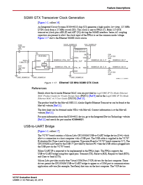
Feature DescriptionsSGMII GTX Transceiver Clock Generation[Figure1-2, callout 16]An Integrated Circuit Systems ICS844021I chip (U2) generates a high-quality, low-jitter, 125MHzLVDS clock from a 25MHz crystal (X3). This clock is sent to FPGA U1, Bank 113 GTXtransceiver (clock pins AH8 (P) and AH7 (N)) driving the SGMII interface. Series AC couplingcapacitors are present to allow the clock input of the FPGA to set the common mode voltage.Figure1-17 shows the Ethernet SGMII clock source.Figure 1-17:Ethernet 125 MHz SGMII GTX ClockReferencesDetails about the tri-mode Ethernet MAC core are provided in LogiCORE IP Tri-Mode EthernetMAC Product Guide for Vivado Design Suite (PG051) [Ref9] and in the LogiCORE IP Tri-ModeEthernet MAC v4.5 User Guide (UG138) [Ref13].The product brief for the Marvell 88E1111 Alaska Gigabit Ethernet Transceiver can be found at theMarvell website [Ref21].The data sheet can be obtained under NDA with Marvell. Contact information is at the Marvellwebsite [Ref21].For more information about the ICS844021 device, go to the Integrated Device Technology website[Ref22] and search for part number ICS844021.USB-to-UART Bridge[Figure1-2, callout 17]The VC707 board contains a Silicon Labs CP2103GM USB-to-UART bridge device (U44) whichallows a connection to a host computer with a USB port. The USB cable is supplied in the VC707Evaluation Kit (Type-A end to host computer, Type mini-B end to VC707 board connector J17). TheCP2103GM is powered by the USB 5V provided by the host PC when the USB cable is plugged intothe USB port on the VC707 board.Xilinx UART IP is expected to be implemented in the FPGA logic. The FPGA supports theUSB-to-UART bridge using four signal pins: Transmit (TX), Receive (RX), Request to Send (RTS),and Clear to Send (CTS).Silicon Labs provides royalty-free Virtual COM Port (VCP) drivers for the host computer. Thesedrivers permit the CP2103GM USB-to-UART bridge to appear as a COM port to communicationsapplication software (for example, TeraTerm) that runs on the host computer. The VCP deviceChapter 1:VC707 Evaluation Board FeaturesTable 1-26:GPIO Connections to FPGA U1 (Cont’d)FPGA (U1) Pin Schematic Net Name I/O Standard GPIO PinAW40GPIO_SW_W LVCMOS18SW7.3A V39GPIO_SW_C LVCMOS18SW6.38-Pole DIP SwitchA V30GPIO_DIP_SW0LVCMOS18SW2.16AY33GPIO_DIP_SW1LVCMOS18SW2.15BA31GPIO_DIP_SW2LVCMOS18SW2.14BA32GPIO_DIP_SW3LVCMOS18SW2.13AW30GPIO_DIP_SW4LVCMOS18SW2.12AY30GPIO_DIP_SW5LVCMOS18SW2.11BA30GPIO_DIP_SW6LVCMOS18SW2.10BB31GPIO_DIP_SW7LVCMOS18SW2.9User Rotary SwitchAT31ROTARY_INCB LVCMOS18SW10.6AW31ROTARY_PUSH LVCMOS18SW10.5AR33ROTARY_INCA LVCMOS18SW10.1User SMAAN31USER_SMA_GPIO_P LVCMOS18J33.1AP31USER_SMA_GPIO_N LVCMOS18J34.1Switches[Figure1-2, callout 27 - 28]The VC707 board Evaluation Board includes a power and a configuration switch:•Power On/Off Slide Switch SW12 (callout 27)•FPGA_PROG_B SW9, active-Low (callout 28)Power On/Off Slide Switch SW12[Figure1-2, callout 27]The VC707 board power switch is SW12. Sliding the switch actuator from the Off to On positionapplies 12V power from J18, a 6-pin mini-fit connector. Green LED DS16 illuminates when theVC707 board power is on. See Power Management for details on the onboard power system.Caution!Do NOT plug a PC ATX power supply 6-pin connector into J18 on the VC707 board.The ATX 6-pin connector has a different pinout than J18. Connecting an ATX 6-pin connectorinto J18 will damage the VC707 board and void the board warranty.Feature DescriptionsThe VC707 Evaluation Kit provides the adapter cable shown in Figure 1-29 for powering the VC707 board from the ATX power supply 4-pin peripheral connector. The Xilinx part number for this cable is 2600304, and is equivalent to Sourcegate Technologies part number AZCBL-WH-1109-RA4. For information on ordering this cable, see [Ref 27].Figure 1-30 shows the power connector J18, power switch SW12 and indicator LED DS16.FPGA_PROG_B Pushbutton SW9 (Active-Low)[Figure 1-2, callout 28]Switch SW9 grounds the FPGA's PROG_B pin when pressed. This action initiates an FPGA reconfiguration. The FPGA_PROG_B signal is connected to FPGA U1 pin AJ11.See 7Series FPGAs Configuration User Guide (UG470) [Ref 3] for further details on configuring the 7series FPGAs.Figure 1-31 shows SW9.Figure 1-29:ATX Power Supply Adapter CableFigure 1-30:Power On/Off Switch SW15UG885_c1_26_030512To A TX 4-Pin Peripheral Power ConnectorTo J18 on VC707 BoardUG885_c1_27_030512VCC12_P_INVCC12_PR2791k Ω1%INPUT_GND1234SW12GND C320330μF 25V C4711μF 25VGNDDS1656J1812345612V N/C COM 12V N/C COMINPUT_GNDPowerPCIeU73138765Appendix B:VITA 57.1 FMC Connector PinoutsAppendix C:Xilinx Constraints File。
FPGA可编程逻辑器件芯片XC2S200-5FG456C中文规格书
0
SHIFT-IR
0
1 EXIT1-IR 1
0
PAUSE-IR
0
1 0 EXIT2-IR
1
UPDATE-IR
1
0
NOTE: The value shown adjacent to each state transition in this figure represents the signal present at TMS at the time of a rising edge at TCK.
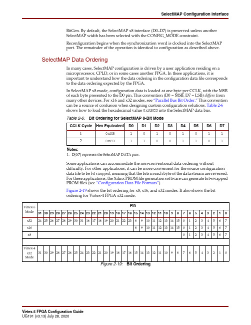
Table 2-6: Bit Ordering for SelectMAP 8-Bit Mode
CCLK Cycle Hex Equivalent D0 D1 D2 D3 D4 D5 D6 D7
1
0xAB
1
0
1
0
1
0
1
1
2
0xCD
1
1
0
0
1
1
0
1
Notes: 1. D[0:7] represent the SelectMAP DATA pins.
For details on the standard Boundary-Scan instructions EXTEST, INTEST, and BYPASS, refer to the IEEE Standard.
Virtex-5 FPGA Configuration Guide UG191 (v3.13) July 28, 2020
UG191_c3_02_050406
Figure 3-2: Boundary-Scan TAP Controller
Virtex-5 devices support the mandatory IEEE 1149.1 commands, as well as several Xilinx vendor-specific commands. The EXTEST, INTEST, SAMPLE/PRELOAD, BYPASS, IDCODE, USERCODE, and HIGHZ instructions are all included. The TAP also supports internal user-defined registers (USER1, USER2, USER3, and USER4) and configuration/readback of the device.
FPGA可编程逻辑器件芯片XC2V80-4FF896I中文规格书
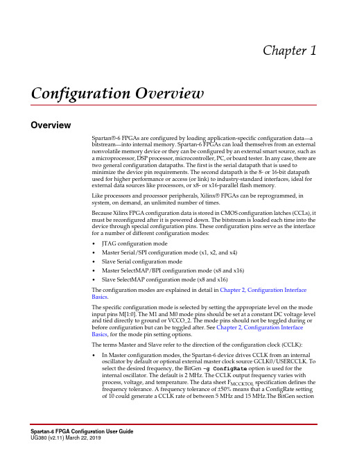
Chapter1 Configuration OverviewOverviewSpartan®-6 FPGAs are configured by loading application-specific configuration data—abitstream—into internal memory. Spartan-6 FPGAs can load themselves from an externalnonvolatile memory device or they can be configured by an external smart source, such asa microprocessor, DSP processor, microcontroller, PC, or board tester. In any case, there aretwo general configuration datapaths. The first is the serial datapath that is used tominimize the device pin requirements. The second datapath is the 8- or 16-bit datapathused for higher performance or access (or link) to industry-standard interfaces,ideal forexternal data sources like processors, or x8- or x16-parallel flash memory.Like processors and processor peripherals, Xilinx® FPGAs can be reprogrammed, insystem, on demand, an unlimited number of times.Because Xilinx FPGA configuration data is stored in CMOS configuration latches (CCLs), itmust be reconfigured after it is powered down. The bitstream is loaded each time into thedevice through special configuration pins. These configuration pins serve as the interfacefor a number of different configuration modes:•JTAG configuration mode•Master Serial/SPI configuration mode (x1, x2, and x4)•Slave Serial configuration mode•Master SelectMAP/BPI configuration mode (x8 and x16)•Slave SelectMAP configuration mode (x8 and x16)The configuration modes are explained in detail in Chapter2, Configuration InterfaceBasics.The specific configuration mode is selected by setting the appropriate level on the modeinput pins M[1:0]. The M1 and M0 mode pins should be set at a constant DC voltage leveland tied directly to ground or VCCO_2. The mode pins should not be toggled during orbefore configuration but can be toggled after. See Chapter2, Configuration InterfaceBasics, for the mode pin setting options.The terms Master and Slave refer to the direction of the configuration clock (CCLK):•In Master configuration modes, the Spartan-6 device drives CCLK from an internaloscillator by default or optional external master clock source GCLK0/USERCCLK. Toselect the desired frequency, the BitGen -g ConfigRate option is used for theinternal oscillator. The default is 2MHz. The CCLK output frequency varies withprocess, voltage, and temperature. The data sheet F MCCKTOL specification defines thefrequency tolerance. A frequency tolerance of ±50% means that a ConfigRate settingof 10 could generate a CCLK rate of between 5MHz and 15MHz.The BitGen sectionChapter 3:Boundary-Scan and JTAG ConfigurationChapter 4:User PrimitivesTable 4-1:BSCAN_SPARTAN6 Port Descriptions (Cont’d)Signal Name Type FunctionTCK Output The value of the TCK input pin to the FPGA.TMS Output The value of the TMS input pin to the FPGA.TDO Input TDO input driven from the user fabric logic. This signal isinternally sampled on the falling edge before being driven outto the FPGA TDO pin.ICAP_SPARTAN6The ICAP_SPARTAN6 primitive works similarly to the SelectMAP configuration interfaceexcept it is on the fabric side, and ICAP has a separate read/write bus, as opposed to thebidirectional bus in SelectMAP. ICAP also only supports x16 data width. The generalSelectMAP timing diagrams and the SelectMAP bitstream ordering information, asdescribed in SelectMAP Configuration Interface, page30, are also applicable to ICAP. Itallows the user to access configuration registers and readback configuration data afterconfiguration is done.ICAP data width is 16bits for both input and output.Table 4-2:ICAP_SPARTAN6 Port DescriptionsSignal Type FunctionCLK Input ICAP interface clock.CE Input Active-Low ICAP interface select. Equivalent to CSI_B in theSelectMAP interface.WRITE Input Read/Write control input. 0=WRITE, 1=READ. Equivalent tothe RDWR_B signal in the SelectMAP interface.I[15:0]Input16-bit-wide ICAP write data bus. The bit ordering is identical tothe SelectMAP interface. See SelectMAP Data Ordering, page39.O[15:0]Output16-bit-wide ICAP read data bus. The bit ordering is identical to theSelectMAP interface. See SelectMAP Data Ordering in SelectMAPData Ordering, page39. The ICAP output should be captured in adevice register.The packet buffer must be cleared for read data from a commandto be presented on the O[15:0] bus. See Configuration RegisterRead Procedure (SelectMAP) and Configuration Memory ReadProcedure (SelectMAP) for the correct procedure.BUSY Output Active-High busy status. Only used in read operations. BUSYremains Low during writes.STARTUP_SPARTAN6STARTUP_SPARTAN6The STARTUP_SPARTAN6 primitive provides a fabric interface to allow users to controlsome of global signals after configuration.Table 4-3:STARTUP_SPARTAN6 Port DescriptionSignal Name Type FunctionEOS Output Active-High. Absolute end of startup.CLK Input User startup clock.GSR Input Active-High global set/reset signal. When thisinput is asserted, all flip-flops are restored to theirinitial value in the bitstream.KEYCLEARB Input Clear the battery-backed RAM key when it is set.This signal needs to stay Low for 200ns (four clockcycles) to enable KEYCLEAR function.GTS Input Active-High global 3-state signal. When this input isasserted, all user I/Os are 3-stated.CFGMCLK Output Configuration internal oscillator clock output ofapproximately 50MHz that can be used as a genericclock source instead of a ring oscillator in the FPGAlogic. If this port is not connected in the design, theoscillator is disabled.CFGCLK Output Configuration logic main clock output. This signaloutputs the clock associated with the currentconfiguration mode. If the FPGA is in a Slaveconfiguration mode, the clock source is CCLK. If theFPGA is in a Master configuration mode, the clocksource is the internal oscillator frequency (asdefined by the BitGen option -g ConfigRate).Use the BitGen Persist option to maintain thissignal after configuration.DNA_PORTThe DNA_PORT provides access to a dedicated shift register, which can be loaded with theDevice DNA data bits (unique ID) for a given Spartan®-6device. In addition to shiftingout the DNA data bits, this component allows for the inclusion of supplemental data bitsfor additional user data or allow for the DNA data to rollover (repeat DNA data afterinitial data has been shifted out). This component is primarily used in conjunction withother circuitry to build anti-cloning protection for the FPGA bitstream from possible theft.The DNA_PORT component must be instantiated to be used in a design. The instantiationtemplate is found within the ISE® software. Project Navigator HDL templates. Theinstance declaration must be placed within the code. All inputs and outputs must beconnected to the design to ensure proper operation.To access the Device DNA data, the shift register must first be loaded by setting theactive-High READ signal for one clock cycle. After the shift register is loaded, the data canbe synchronously shifted out by enabling the active-High SHIFT input and capturing thedata from the DOUT output port. If desired, additional data can be appended to the end ofthe 57-bit shift register by connecting the appropriate logic to the DIN port. If DNA dataChapter 4:User Primitives。
FPGA可编程逻辑器件芯片XC2S200-5FGG456I中文规格书
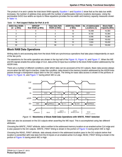
The product of w and n yields the total block RAM capacity. Equation 1 and Equation 2 show that as the data bus width increases, the number of address lines along with the number of addressable memory locations decreases. Using the permissible DI/DO bus widths as inputs to these equations provides the bus width and memory capacity measures shown in T able 14.Block RAM Data OperationsWriting data to and accessing data from the block RAM are synchronous operations that take place independently on eachof the two ports.The waveforms for the write operation are shown in the top half of the Figure 15, Figure 16, and Figure 17. When the WE and EN signals enable the active edge of CLK, data at the DI input bus is written to the block RAM location addressed by the ADDR lines.There are a number of different conditions under which data can be accessed at the DO outputs. Basic data access always occurs when the WE input is inactive. Under this condition, data stored in the memory location addressed by the ADDR lines passes through a transparent output latch to the DO outputs. The timing for basic data access is shown in the portions of Figure 15, Figure 16, and Figure 17 during which WE is Low.Data can also be accessed on the DO outputs when asserting the WE input. This is accomplished using two different attributes:Choosing the WRITE_FIRST attribute, data is written to the addressed memory location on an enabled active CLK edge and is also passed to the DO outputs. WRITE_FIRST timing is shown in the portion of Figure 15 during which WE is High.Choosing the READ_FIRST attribute, data already stored in the addressed location pass to the DO outputs before that location is overwritten with new data from the DI inputs on an enabled active CLK edge. READ_FIRST timing is shown in the portion of Figure 16 during which WE is High.Table 14:Port Aspect Ratios for Port A or BDI/DO Bus Width (w – p Bits)DIP/DOP Bus Width (p Bits)Total Data Path Width (w Bits)ADDR Bus Width(r Bits)No. of Addressable Locations (n)Block RAM Capacity (Bits)1011416,38416,384202138,19216,384404124,09616,384819112,04818,43216218101,02418,43232436951218,432Figure 15:Waveforms of Block RAM Data Operations with WRITE_FIRST SelectedFigure 16:Waveforms of Block RAM Data Operations with READ_FIRST SelectedChoosing a third attribute called NO_CHANGE puts the DO outputs in a latched state when asserting WE. Under this condition, the DO outputs will retain the data driven just before WE was asserted. NO_CHANGE timing is shown in the portion of Figure17 during which WE is High.Figure 17:Waveforms of Block RAM Data Operations with NO_CHANGE SelectedDedicated MultipliersAll Spartan-3 devices provide embedded multipliers that accept two 18-bit words as inputs to produce a 36-bit product. This section provides an introduction to multipliers. For further details, refer to the chapter entitled “Using Embedded Multipliers” in UG331.The input buses to the multiplier accept data in two’s-complement form (either 18-bit signed or 17-bit unsigned). One such multiplier is matched to each block RAM on the die. The close physical proximity of the two ensures efficient data handling. Cascading multipliers permits multiplicands more than three in number as well as wider than 18-bits. The multiplier is placed in a design using one of two primitives: an asynchronous version called MULT18X18 and a version with a register called MULT18X18S, as shown in Figure18. The signals for these primitives are defined in T able15.The CORE Generator system produces multipliers based on these primitives that can be configured to suit a wide range of requirements.Digital Clock Manager (DCM)Spartan-3 devices provide flexible, complete control over clock frequency, phase shift and skew through the use of the DCM feature. T o accomplish this, the DCM employs a Delay-Locked Loop (DLL), a fully digital control system that uses feedback to maintain clock signal characteristics with a high degree of precision despite normal variations in operating temperature and voltage. This section provides a fundamental description of the DCM. For further information, refer to the chapter entitled “Using Digital Clock Managers” in UG331.Each member of the Spartan-3 family has four DCMs, except the smallest, the XC3S50, which has two DCMs. The DCMs are located at the ends of the outermost Block RAM column(s). See Figure 1, page 3. The Digital Clock Manager is placed in a design as the “DCM” primitive.The DCM supports three major functions: •Clock-skew Elimination: Clock skew describes the extent to which clock signals may, under normal circumstances,deviate from zero-phase alignment. It occurs when slight differences in path delays cause the clock signal to arrive at different points on the die at different times. This clock skew can increase set-up and hold time requirements as well as clock-to-out time, which may be undesirable in applications operating at a high frequency, when timing is critical. The DCM eliminates clock skew by aligning the output clock signal it generates with another version of the clock signal that is fed back. As a result, the two clock signals establish a zero-phase relationship. This effectively cancels out clock distribution delays that may lie in the signal path leading from the clock output of the DCM to its feedback input.•Frequency Synthesis: Provided with an input clock signal, the DCM can generate a wide range of different output clock frequencies. This is accomplished by either multiplying and/or dividing the frequency of the input clock signal by any of several different factors.Figure 18:Embedded Multiplier PrimitivesTable 15:Embedded Multiplier Primitives DescriptionsSignal Name Direction FunctionA[17:0]Input Apply one 18-bit multiplicand to these inputs. The MULT18X18S primitive requires a setup time before the enabled rising edge of CLK.B[17:0]Input Apply the other 18-bit multiplicand to these inputs. The MULT18X18S primitive requires a setup time before the enabled rising edge of CLK.P[35:0]Output The output on the P bus is a 36-bit product of the multiplicands A and B. In the case of the MULT18X18S primitive, an enabled rising CLK edge updates the P bus.CLK Input (1)CLK is only an input to the MULT18X18S primitive. The clock signal applied to this input, when enabled by CE, updates the output register that drives the P bus.CE Input (1)CE is only an input to the MULT18X18S primitive. Enable for the CLK signal. Asserting this input enables the CLK signal to update the P bus.RST Input (1)RST is only an input to the MULT18X18S primitive. Asserting this input resets the output register on an enabled, rising CLK edge, forcing the P bus to all zeroes.Notes:1.The control signals CLK, CE and RST have the option of inverted polarity.Spartan-3 FPGA Family: DC and Switching CharacteristicsSpartan-3 FPGA Family: Pinout Descriptions。
FPGA可编程逻辑器件芯片XC2S150-4FG456C中文规格书
Chapter1 Introduction to the RocketIO GTX TransceiverOverviewThe RocketIO™ GTX transceiver is a power-efficient transceiver for Virtex®-5 FPGAs. TheGTX transceiver is highly configurable and tightly integrated with the programmable logicresources of the FPGA. It provides the following features to support a wide variety ofapplications:•Current Mode Logic (CML) serial drivers/buffers with configurable termination,voltage swing, and coupling.•Programmable TX pre-emphasis, RX equalization, and linear and decision feedbackequalization (DFE) for optimized signal integrity.•Line rates from 750Mb/s to 6.5Gb/s, with optional 5x digital oversampling requiredfor rates between 150Mb/s and 750Mb/s. The nominal operation range of the sharedPMA PLL is from 1.5GHz to 3.25GHz. These are nominal values, see DS202: Virtex-5FPGA Data Sheet for specifications.•Optional built-in PCS features, such as 8B/10B encoding, comma alignment, channelbonding, and clock correction.•Fixed latency modes for minimized, deterministic datapath latency.•Beacon signaling for PCI Express® designs and Out-of-Band signaling includingCOM signal support for SATA designs.•RX/TX Gearbox provides header insertion and extraction support for 64B/66B and64B/67B (Interlaken) protocols.•Receiver eye scan:♦Vertical eye scan in the voltage domain for testing purposes♦Horizontal eye scan in the time domain for testing purposesThe first-time user is recommended to read High-Speed Serial I/O Made Simple[Ref1], whichdiscusses high-speed serial transceiver technology and its applications.Table1-1 lists some of the standard protocols designers can implement using the GTXtransceiver. The Xilinx® CORE Generator™ tool includes a Wizard to automaticallyconfigure GTX transceivers to support one of these protocols or perform customconfiguration (see Chapter2, “RocketIO GTX Transceiver Wizard”).The GTX_DUAL tile offers a data rate range and features that allow physical layer supportfor various protocols as illustrated in Table1-1.Preface:About This GuideAdditional Documentation•Virtex-5 Family OverviewThe features and product selection of the Virtex-5 family are outlined in this overview.•Virtex-5 FPGA Data Sheet: DC and Switching CharacteristicsThis data sheet contains the DC and Switching Characteristic specifications for theVirtex-5 family.•Virtex-5 FPGA User GuideThis user guide includes chapters on:♦Clocking Resources♦Clock Management Technology (CMT)♦Phase-Locked Loops (PLLs)♦Block RAM♦Configurable Logic Blocks (CLBs)♦SelectIO™ Resources♦SelectIO Logic Resources♦Advanced SelectIO Logic Resources•Virtex-5 FPGA RocketIO GTP Transceiver User GuideThis guide describes the RocketIO™ GTP transceivers available in the Virtex-5 LXTand SXT platforms.•Virtex-5 FPGA Embedded Processor Block for PowerPC® 440 DesignsThis reference guide is a description of the embedded processor block available in theVirtex-5 FXT platform.•Virtex-5 FPGA Tri-Mode Ethernet Media Access ControllerThis guide describes the dedicated Tri-Mode Ethernet Media Access Controlleravailable in the Virtex-5 LXT, SXT, FXT, and TXT platforms.•Virtex-5 FPGA Integrated Endpoint Block User Guide for PCI Express DesignsThis guide describes the integrated Endpoint blocks in the Virtex-5 LXT, SXT, FXT, andTXT platforms used for PCI Express® designs.•XtremeDSP Design ConsiderationsThis guide describes the XtremeDSP™ slice and includes reference designs for usingthe DSP48E slice.•Virtex-5 FPGA Configuration GuideThis all-encompassing configuration guide includes chapters on configurationinterfaces (serial and SelectMAP), bitstream encryption, Boundary-Scan and JTAGconfiguration, reconfiguration techniques, and readback through the SelectMAP andJTAG interfaces.•Virtex-5 FPGA System Monitor User GuideThe System Monitor functionality available in all the Virtex-5 devices is outlined inthis guide.Additional Support Resources•Virtex-5 FPGA Packaging and Pinout SpecificationsThis specification includes the tables for device/package combinations and maximumI/Os, pin definitions, pinout tables, pinout diagrams, mechanical drawings, andthermal specifications.•Virtex-5 FPGA PCB Designer’s GuideThis guide provides information on PCB design for Virtex-5 devices, with a focus onstrategies for making design decisions at the PCB and interface level.The following documents provide supplemental material useful to this user guide:1.Athavale, Abhijit and Carl Christensen. High-Speed Serial I/O Made Simple.2.UG200, Embedded Processor Block in Virtex-5 FPGAs Reference Guide.3.UG626, Synthesis and Simulation Design Guide.4.Granberg, Tom. Handbook of Digital Techniques for High-Speed Design. Prentice-Hall. ISBN-10:1-13-142291-X. ISBN-13: 978-0131422919.5.Grover, Frederick W., Ph.D. 1946. Inductance Calculations: Working Formulas and Tables. NewYork: D. Van Nostrand Company, Inc.6.Johnson, Howard, Martin Graham. High-Speed Signal Propagation: Advanced Black Magic.Prentice-Hall. ISBN-10: 0-13-084408-X. ISBN-13: 978-0130844088.7.Montrose, Mark I. 1999. EMC and the Printed Circuit Board. The Institute of Electrical andElectronics Engineers, Inc. ISBN 0-7803-4703-X.8.Smith, Larry D. November 1984. Decoupling Capacitor Calculations for CMOS Circuits.Proceedings EPEP Conference.9.Williams, Ross N. The Painless Guide to CRC Error Detection Algorithms.10.Schlichthaerle, Dietrich. Digital Filters: Basics and Design. Springer. ISBN-10 3-540-66841-1.11.DS083, Virtex-II Pro and Virtex-II Pro X Platform FPGAs Complete Data Sheet.12.UG024, RocketIO Transceiver User Guide.13.UG076, Virtex-4 RocketIO Multi-Gigabit Transceiver User Guide.14.XAPP209, IEEE 802.3 Cyclic Redundancy Check.15.XAPP562, Configurable LocalLink CRC Reference Design.16.UG196, Virtex-5 FPGA RocketIO GTP Transceiver User Guide.17.UG204, LogiCORE IP Virtex-5 FPGA RocketIO GTX Transceiver Wizard v1.6 Getting StartedGuide.Additional Support ResourcesPreface:About This GuideSection 1: FPGA Level Design。
FPGA可编程逻辑器件芯片XC2S300E-FG456中文规格书
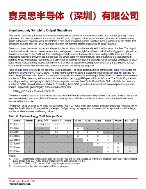
FPGA可编程逻辑器件芯片XC2V1000-4FG456C中文规格书
© Copyright 2012-2013 Xilinx, Inc. Xilinx, the Xilinx logo, Artix, ISE, Kintex, Spartan, Virtex, Zynq, and other designated brands included herein are trademarks of Xilinx in the United States and other countries. All other trademarks are the property of their respective owners.XCN12026 (v1.0.2) April 24, 2013 1XCN12026 (v1.0.2) April 24, 2013 Product Discontinuation Notice OverviewThis notification is to communicate that Xilinx is discontinuing certain Virtex ® (Virtex-E/-EM, Virtex-II and EasyPath ™ Virtex-II families) and Spartan ® (Spartan-IIE family) FPGA products due to supplier line discontinuance. The XC17V00 PROMs family has also been identified for obsolescence in this notice as part of the regular product pruning activities.DescriptionXilinx retracted PDN Notice XCN11003 in September 2011 with a two year extension of production capability. This notification is to inform customers that the extension for Virtex ® (Virtex-E/-EM, Virtex-II and EasyPath™ Virtex -II families) and Spartan ® (Spartan-IIE family) FPGA products listed in XCN11003 is ending.This product discontinuance notice (PDN) applies to all temperature grades and variants (XC, XA and XQ part numbers) of the Spartan-IIE FPGA, Virtex-E/-EM, Virtex-II and EasyPath and Virtex-II FPGA families.As for XC17V00 PROMs, it applies to all temperature grades and variants for XC part numbers only.In this specific notice, Xilinx is offering extended Last Time Ship period from standard six months to sixteen months. Products AffectedThe products affected included all standard part numbers and specification control document (SCD) versions of the standard part numbers listed in this notice.∙Configuration Solutions PROMs Family Products Affected ∙Spartan-IIE Family FPGA Commercial Products Affected ∙Virtex-E/-EM Family FPGA Commercial Products Affected ∙Virtex-II Family FPGA Commercial Products Affected ∙EasyPath Virtex-II Family FPGA Products Affected ∙Automotive (XA) Spartan-IIE Family FPGA Products Affected ∙Automotive IQ Spartan-IIE Family FPGA Products Affected ∙HiRel (XQ) Family FPGA Products Affected ∙Appendix A – All SCD Products AffectedKey Dates and Ordering InformationFinal orders (LTB) are accepted until May 31, 2013.Orders placed after March 31, 2013 will be Non-Cancellable, Non-Returnable (NCNR).Final deliveries (LTS) must occur on or before September 30, 2014.RMAs for replacement devices will be accepted until March 31, 2015.Product Discontinuation Notice: Spartan-IIE, Virtex-E, Virtex-EM, Virtex-II, EasyPath Virtex-II FPGA and PROMs ProductsXCN12026 (v1.0.2) April 24, 2013 7Product Discontinuation Notice: Spartan-IIE, Virtex-E, Virtex-EM, Virtex-II, EasyPath Virtex-II FPGA and PROMs Products 8 XCN12026 (v1.0.2) April 24, 2013。
FPGA可编程逻辑器件芯片XC2V500-6FGG256C中文规格书
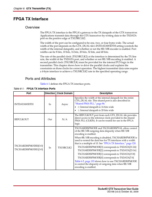
Chapter 6:GTX Transmitter (TX)FPGA TX InterfaceOverviewThe FPGA TX interface is the FPGA’s gateway to the TX datapath of the GTX transceiver.Applications transmit data through the GTX transceiver by writing data to the TXDATAport on the positive edge of TXUSRCLK2.The width of the port can be configured to be one, two, or four bytes wide. The actualwidth of the port depends on the GTX_DUAL tile's INTDATAWIDTH setting (controls thewidth of the internal datapath), and whether or not the 8B/10B encoder is enabled. Portwidths can be 8 bits, 10 bits, 16 bits, 20 bits, 32 bits, and 40 bits.The rate of the parallel clock (TXUSRCLK2) at the interface is determined by the TX linerate, the width of the TXDATA port, and whether or not 8B/10B encoding is enabled. Asecond parallel clock (TXUSRCLK) must be provided for the internal PCS logic in thetransmitter. This chapter shows how to drive the parallel clocks and explains theconstraints on those clocks for correct operation. The highest transmitter data rates requirea 4-byte interface to achieve a TXUSRCLK2 rate in the specified operating range.Ports and AttributesTable6-1 defines the FPGA TX interface ports.Table 6-1:FPGA TX Interface PortsPort Direction Clock Domain DescriptionINTDATAWIDTH In Async Specifies the width of the internal datapath for the entire GTX_DUAL tile. This shared port is also described in “Shared PMA PLL,” page 86.•0: Internal datapath is 16 bits wide•1: Internal datapath is 20 bits wideREFCLKOUT Out N/A The REFCLKOUT port from each GTX_DUAL tile provides direct access to the reference clock provided to the shared PMA PLL (CLKIN). It can be routed for use in the FPGA logic.TXCHARDISPMODE0[3:0] TXCHARDISPMODE1[3:0]In TXUSRCLK2TXCHARDISPMODE and TXCHARDISPVAL allow controlof the 8B/10B outgoing data disparity when 8B/10Bencoding is enabled.When 8B/10B encoding is disabled, TXCHARDISPMODE isused to extend the data bus for TX interfaces with a widththat is a multiple of 10. See “FPGA TX Interface,” page 120.TXCHARDISPMODE[3] corresponds to TXDATA[31:24]TXCHARDISPMODE[2] corresponds to TXDATA[23:16]TXCHARDISPMODE[1] corresponds to TXDATA[15:8]TXCHARDISPMODE[0] corresponds to TXDATA[7:0]Table6-5, page133 shows how to use TXCHARDISPMODEto control the disparity of outgoing data when 8B/10Bencoding is enabled.FPGA TX InterfaceTXCHARDISPVAL0[3:0] TXCHARDISPVAL1[3:0]In TXUSRCLK2TXCHARDISPVAL and TXCHARDISPMODE allow controlof the 8B/10B outgoing data disparity when 8B/10Bencoding is enabled.When 8B/10B encoding is disabled, TXCHARDISPVAL isused to extend the data bus for 10- and 20-bit TX interfaces.See “FPGA TX Interface,” page 120.TXCHARDISPVAL[3] corresponds to TXDATA[31:24]TXCHARDISPVAL[2] corresponds to TXDATA[23:16]TXCHARDISPVAL[1] corresponds to TXDATA[15:8]TXCHARDISPVAL[0] corresponds to TXDATA[7:0]Table6-5, page133 shows how to use TXCHARDISPVAL tocontrol the disparity of outgoing data when 8B/10Bencoding is enabled.TXDATA0[31:0] TXDATA1[31:0]In TXUSRCLK2The bus for transmitting data. The width of this port dependson TXDATAWIDTH:•TXDATAWIDTH = 0: TXDATA[7:0] = 8 bits wide•TXDATAWIDTH = 1: TXDATA[15:0] = 16 bits wide•TXDATAWIDTH = 2: TXDATA[31:0] = 32 bits wideWhen a 10-bit, 20-bit, or 40-bit bus is required, theTXCHARDISPVAL and TXCHARDISPMODE ports from the8B/10B encoder are concatenated with the TXDATA port. SeeFigure6-3, page123.TXDATAWIDTH0[1:0] TXDATAWIDTH1[1:0]In TXUSRCLK2Selects the width of the TXDATA port.•0: TXDATA is 8 bits or 10 bits wide•1: TXDATA is 16 bits or 20 bits wide•2: TXDATA is 32 bits or 40 bits wide•3: ReservedTXENC8B10BUSE0 TXENC8B10BUSE1In TXUSRCLK2TXENC8B10BUSE is set High to enable the 8B/10B encoder.INTDATAWIDTH must also be High.0: 8B/10B encoder bypassed. This option reduces latency.1: 8B/10B encoder enabled. INTDATAWIDTH must beHigh.TXOUTCLK0 TXOUTCLK1Out N/AThis port provides a parallel clock generated by the GTXtransceiver. This clock can be used to drive TXUSRCLK forone or more GTX transceivers. The rate of the clock dependson INTDATAWIDTH:•INTDATAWIDTH is Low: F TXOUTCLK = Line Rate/16•INTDATAWIDTH is High: F TXOUTCLK = Line Rate/20Note:•When INTDATAWIDTH is High, the duty cycle is 60/40instead of 50/50.•When oversampling is enabled, the line rate in thecalculation of F TXOUTCLK is equal to the oversampled linerate, not the PMA line rate.Table 6-1:FPGA TX Interface Ports (Cont’d)Port Direction Clock Domain DescriptionTX Out-of-Band/Beacon SignalingRX OOB/Beacon SignalingTable7-14 defines the RX OOB/beacon signaling attributes.Table 7-14:RX OOB/Beacon Signaling AttributesAttribute Type DescriptionOOB_CLK_DIVIDER Integer Sets the squelch clock rate. The squelch clock must be set between 25MHz and 37.5MHz, as close to 25MHz as possible for the SATA OOB detector to work correctly.Squelch Clock rate = CLKIN/OOB_CLK_DIVIDERValid divider settings are 1, 2, 4, 6, 8, 10, 12, and 14.OOBDETECT_THRESHOLD_0 OOBDETECT_THRESHOLD_13-bit BinarySets the minimum differential voltage between RXN and RXP.When the differential voltage drops below this level, theincoming signal is considered an OOB signal. This 3-bit binaryencoded attribute has the following nominal values of the OOBthreshold voltage(1):Value OOB Nominal Threshold Voltage [mV]000 – 101Not supported110 (default)9011195RX_STATUS_FMT_0 RX_STATUS_FMT_1StringDefines which status encoding is used:PCIE: PCI Express encodingSATA: SATA encodingSATA_BURST_VAL_0 SATA_BURST_VAL_13-bit BinaryNumber of bursts required to declare a COM match. The defaultfor SATA_BURST_VAL is 4, which is the burst count specified inSATA for COMINIT, COMRESET, and COMWAIT.SATA_IDLE_VAL_0 SATA_IDLE_VAL_13-bit BinaryNumber of idles required to declare a COM match. Each idle is anOOB signal with a length that matches eitherCOMINIT/COMRESET or COMWAIT. When the SATA detectorstarts to count one type of idle (for example,COMRESET/COMINIT), it resets the count if it receives the othertype. This value defaults to 3 to match the SATA specification.SATA_MAX_BURST_0 SATA_MAX_BURST_1IntegerSets the threshold for the SATA detector to reject a burst in termsof squelch clock cycles. SATA_MAX_BURST has valid valuesbetween 1 and 61 (the default is 7) and must be greater thanSATA_MIN_BURST. See the “Description” section to learn howto calculate the best value for a given squelch clock rate.SATA_MAX_INIT_0 SATA_MAX_INIT_1IntegerSets the maximum time allowed for a COMINIT/COMRESETidle for the SATA detector in terms of squelch clock cycles.SATA_MAX_INIT has valid values between 1 and 61 (the defaultis 22) and must be greater than SATA_MIN_INIT. See the“Description” section to learn how to calculate the best value fora given squelch clock rate.SATA_MAX_WAKE_0 SATA_MAX_WAKE_1IntegerSets the maximum time allowed for a COMWAKE idle for theSATA detector in terms of squelch clock cycles.SATA_MAX_WAKE has valid values between 1 and 61 (thedefault is 7) and must be greater than SATA_MIN_WAKE. See the“Description” section to learn how to calculate the best value fora given squelch clock rate.Configurable Loss-of-Sync State Machine。
- 1、下载文档前请自行甄别文档内容的完整性,平台不提供额外的编辑、内容补充、找答案等附加服务。
- 2、"仅部分预览"的文档,不可在线预览部分如存在完整性等问题,可反馈申请退款(可完整预览的文档不适用该条件!)。
- 3、如文档侵犯您的权益,请联系客服反馈,我们会尽快为您处理(人工客服工作时间:9:00-18:30)。
Chapter 1:Configuration Overviewwidth. Table1-5 shows an example bitstream with an inserted bus width detection pattern.When observing the pattern on the FPGA data pin, the bits are bit swapped, as describedin “Parallel Bus Bit Order.”The bitstream data in Table1-5 shows the 32-bit configuration word for an unswappedbitstream. For a swapped bitstream format, the LSB and MSB order for the individual bytesare swapped. For example, the Sync word at the FPGA pins in the D[31:00] bit order wouldbe: 0x5599AA66. For swapped and unswapped formats see “Configuration Data FileFormats.”.Table 1-5:Bus Width Detection PatternD[24:31]D[16:23]D[8:15]D[0:7]Comments0xFF0xFF0xFF0xFF0x000x000x000xBB Bus Width Pattern0x110x220x000x44Bus Width Pattern0xFF0xFF0xFF0xFF0xFF0xFF0xFF0xFF0xAA0x990x550x66Sync Word……………Bus width auto detection is transparent to most users, because all configuration bitstreams(BIT or RBT files) generated by the Xilinx ISE® Bitstream Generator (BitGen) softwareinclude the Bus Width Auto Detection pattern. These patterns are ignored by theconfiguration logic if the Mode pins are set to Master Serial, Slave Serial, JTAG, or SPImode.For the x8 bus, the configuration bus width detection logic first finds 0xBB on the D[0:7]pins, followed by 0x11. For the x16 bus, the configuration bus width detection logic firstfinds 0xBB on D[0:7] followed by 0x22. For the x32 bus, the configuration bus widthdetection logic first finds 0xBB, on D[0:7], followed by 0x44.If the immediate byte after 0xBB is not 0x11, 0x22, or 0x44, the bus width state machine isreset to search for the next 0xBB until a valid sequence is found. Then it switches to theappropriate external bus width and starts looking for the Sync word.Sync WordA special Sync word is used to allow configuration logic to align at a 32-bit word boundary.No packet processed by the FPGA until the Sync word is found. The bus width must bedetected successfully for parallel configuration modes before the Sync word can bedetected. Table1-6 shows the Sync word in an unswapped bitstream format.Table 1-6:Sync Word31:2423:1615:87:00xAA0x990x550x66Generating PROM FilesGenerating PROM FilesPROM files are generated from bitstream files with the PROMGen utility. Users can accessPROMGen directly from the command line or indirectly through the iMPACT FileGeneration Mode. For PROMGen syntax, refer to the Development System Reference Guide.For information on iMPACT, refer to the ISE® Software Documentation). PROM files serveto reformat bitstream files for PROM programming and combine bitstream files for serialdaisy chains (see “PROM Files for Serial Daisy Chains”).PROM Files for Serial Daisy ChainsConfiguration data for serial daisy chains requires special formatting because separate BITfiles cannot simply be concatenated together to program the daisy chain. The specialformatting is performed by PROMGen (or iMPACT) when generating a PROM file frommultiple bitstreams. To generate the PROM file, specify multiple bitstreams using thePROMGen -n, -u, and -d options or the iMPACT File Generation Wizard. Refer tosoftware documentation for details.PROMGen reformats the configuration bitstreams by nesting downstream configurationdata into configuration packets for upstream devices. Attempting to program the chain bysending multiple bitstreams to the first device causes the first device to configure and thenignore the subsequent data.PROM Files for SelectMAP ConfigurationThe MCS file format is most commonly used to program Xilinx configuration PROMs thatin turn program a single FPGA in SelectMAP mode. For custom configuration solutions,the BIN and HEX files are the easiest PROM file formats to use due to their raw data format.In some cases, additional formatting is required; refer to XAPP502, Using a Microprocessorto Configure Xilinx FPGAs via Slave Serial or SelectMAP Mode for details.If multiple configuration bitstreams for a SelectMAP configuration reside on a singlememory device, the bitstreams must not be combined into a serial daisy chain PROM file.Instead, the target memory device should be programmed with multiple BIN or HEX files.If a single PROM file with multiple, separate data streams is needed, one can be generatedin iMPACT by targeting a Parallel PROM, then selecting the appropriate number of datastreams. This can also be accomplished through the PROMGen command line. Refer toPROMGen software documentation for details.For Platform Flash XL-based SelectMAP configuration, use the iMPACT software togenerate an MCS PROM file. Select the Xilinx XCF128X device as the target PROM devicetype for creating the file. See UG438, Platform Flash XL User Guid e, for PROM filegeneration instructions.PROM Files for SPI/BPI ConfigurationThe -d and -u options in PROMGen or the iMPACT File Generation Wizard are used tocreate PROM files for third-party Flash devices. The output format supported by yourthird-party programmer should be chosen. Some BPI devices require endian-swapping tobe enabled when programming the PROM file. Refer to the Flash vendor's documentation.Bit SwappingBit swapping is the swapping of the bits within a byte. The MCS, EXO, and TEK PROM fileformats are always bit swapped. The HEX file format can be bit swapped or not bit4.The PROM in this diagram represents one or more Xilinx PROMs. Multiple PROMscan be cascaded to increase the overall configuration storage capacity.5.The BIT file must be reformatted into a PROM file before it can be stored on thePROM. Refer to the “Generating PROM Files” section.6.On some Xilinx PROMs, the reset polarity is programmable. RESET should beconfigured as active Low when using this setup.7.For ganged serial configuration, all devices must be identical (same IDCODE) andmust be configured with the same bitstream.8.The CCLK net requires Thevenin parallel termination. See “Board Layout forConfiguration Clock (CCLK),” page73.9.Ganged serial configuration is specific to the Platform Flash XCFS and XCFP PROMonly.10.Fallback and Multiboot are not supported in ganged serial configuration.There are a number of important considerations for ganged serial configuration:∙Startup Sequencing (GTS)GTS should be released before DONE or during the same cycle as DONE to ensure all devices are operational when all DONE pins have been released.∙Disable the Active DONE Driver for All DevicesFor ganged serial configuration, the active DONE driver must be disabled for all devices if the DONE pins are tied together, because there can be variations in the startup sequencing of each device. A pull-up resistor is therefore required on the common DONE signal.-g DriveDone:no (BitGen option, all devices)∙Connect all DONE pins if using a Master DeviceIt is important to connect the DONE pins for all devices in ganged serial configuration if one FPGA is used as the Master device. Failing to connect the DONE pins can cause configuration to fail for individual devices in this case. If all devices are set for Slave serial mode, the DONE pins can be disconnected (if the external CCLK sourcecontinues toggling until all DONE pins go High).For debugging purposes, it is often helpful to have a way of disconnecting individual DONE pins from the common DONE signal.∙DONE Pin Rise TimeAfter all DONE pins are released, the DONE pin should rise from logic 0 to logic 1 in one CCLK cycle. If additional time is required for the DONE signal to rise, the BitGen donepipe option can be set for all devices in the serial daisy chain.∙Configuration Clock (CCLK) as Clock Signal for Board LayoutThe CCLK signal is relatively slow, but the edge rates on the Virtex-5 input buffers are very fast. Even minor signal integrity problems on the CCLK signal can cause the configuration to fail. (Typical failure mode: DONE Low and INIT_B High.) Therefore, design practices that focus on signal integrity, including signal integrity simulation with IBIS, are recommended.∙Signal FanoutDesigners must focus on good signal integrity when using ganged serialconfiguration. Signal integrity simulation is recommended.∙PROM Files for Ganged Serial ConfigurationBoard Layout for Configuration Clock (CCLK)。
