印刷电路板实用手册
印刷电路板实用手册

【印制电路板电镀及层压化学类简易实用手册】印制电路板制造技术的飞速发展,促使广大从事印制电路板制造行业的人们,加快知识更新。
为此,就必须掌握必要的新知识并与原有实用的科技成为工作必备的参考资料,更好地从事各种类型的科研工作。
这本手册就是使从事高科技行业新生产者尽快地掌握与印制电路板制造技术相关的知识,更好的理解和应用印制电路板制造方面的所涉及到的实用技术基础知识,为全面掌握印制电路板制造的全过程和所涉及到科学试验提供必要的基础知识和手段。
第一章溶液浓度计算方法在印制电路板制造技术,电镀为其中十分重要的一个环节,各种溶液占了很大的比重,对印制电路板的最终产品质量起到关键的作用。
无论是选购或者自配都必须进行科学计算。
正确的计算才能确保各种溶液的成分在工艺范围内,对确保产品质量起到重要的作用。
根据印制电路板生产的特点,提供六种计算方法供选用。
1.体积比例浓度计算:∙定义:是指溶质(或浓溶液)体积与溶剂体积之比值。
∙举例:1:5硫酸溶液就是一体积浓硫酸与五体积水配制而成。
2.克升浓度计算:∙定义:一升溶液里所含溶质的克数。
∙举例:100克硫酸铜溶于水溶液10升,问一升浓度是多少?100/10=10克/升3.重量百分比浓度计算(1)定义:用溶质的重量占全部溶液重理的百分比表示。
(2)举例:试求3克碳酸钠溶解在100克水中所得溶质重量百分比浓度?4.克分子浓度计算∙定义:一升中含1克分子溶质的克分子数表示。
符号:M、n表示溶质的克分子数、V表示溶液的体积。
如:1升中含1克分子溶质的溶液,它的克分子浓度为1M;含1/10克分子浓度为0.1M,依次类推。
∙举例:将100克氢氧化钠用水溶解,配成500毫升溶液,问这种溶液的克分子浓度是多少?解:首先求出氢氧化钠的克分子数:5. 当量浓度计算∙定义:一升溶液中所含溶质的克当量数。
符号:N(克当量/升)。
∙当量的意义:化合价:反映元素当量的内在联系互相化合所得失电子数或共同的电子对数。
第一讲_印刷电路板教程

看演示
看录象
1、绘制电路图
• • • • A、手工绘制 B、计算机软件绘制 原则: 元件布局合理、美观、方便,线 条布能交叉!
2、准备敷铜板
• • • • 根据需要选用敷铜板 裁剪敷铜板 对敷铜板表面进行清洁处理 (去掉污迹和氧化层)
3、复印电路
• 用新复写纸将电路接线图复写到敷铜 板上, • 注意方向,如果所绘制的原理图是在 元件面绘制的,复写时,一定要将图 纸反过来复写!
绝缘层 顶层 Top 过孔 Via 底层 Bottom 中间层 Mid
2、印刷电路板的结构
焊盘(Pad) 焊盘是印刷电路板用来焊接
电子元件的连接媒介,它将电子元件与电路按 照设计要求接合在一起,从而使电路功能得以 实现。 焊盘的形式按要求有不同大小和形状的,如圆 形、方形、八角形、泪滴形等焊盘。
如何读懂电路图
26
.2 电子工程图的特点
电子工程图主要描述元器件、部件和各部分电路之间
的电气连接及相互关系,应力求简化。 而许多新元件、器件和组件的出现,又会用到新的名 词、符号和代号。因此要及时掌握新器件的符号表示和性 能特点。
如何读懂电路图
27
2 电子工程图的图形符号及说明 2.1 常用图形符号
器、仪表等。
• 3、环氧玻璃布敷铜板
价较高,做高档电器。 于高频电路
基板透明,优于前者,
价高,用
• 4、聚四氟乙烯敷铜板 介质损耗低
返回
印刷电路板图例1
印刷电路板图例2
印刷电路板图例3
二、电路板的制作(手工)
• • • • • • • 基本工序: 1、绘制电路接线图 2、准备敷铜板 3、复印电路 4、描线 5、腐蚀 6、钻孔
印刷电路板讲义资料
图5 选择 PCB编辑器的工作层
格 物 致 新
·厚 德 泽 人
各层含义如下: 1) Signal Layers(信号层)
Protel99 PCB编辑器最多支持以下16个信号层: Top,即顶层,也称为元件面,是元器件的安装 面。在单面板中不能在元件面内布线,只有在双面或 多面板中才允许在元件面内进行少量布线。在单面板 中,由于元件面内没有印制导线,表面安装元件只能 安装在焊锡面上;而在多面板中,包括表面安装元件 在内的所有元件,应尽可能安装在元件面上,但表面 安装元件也可以安装在焊锡面上。
格 物 致 新
·厚 德 泽 人
1、 印制板种类及结构 印制板种类很多,根据导电层数目的 不同,可以将印制板分为单面电路板(简称 单面板)、双面电路板(简称双面板)和多 层电路板;根据覆铜板基底材料的不同,又 可将印制板分为纸质覆铜箔层压板和玻璃布 覆铜箔层压板两大类。此外,采用挠性塑料 作基底的印制板称为挠性印制板,常用做印 制电缆。
格 物 致 新
·厚 德 泽 人
单面板的结构如图1(a)所示,所用的覆 铜板只有一面敷铜箔,另一面空白,因而也 只能在敷铜箔面上制作导电图形。单面板上 的导电图形主要包括固定、连接元件引脚的 焊盘和实现元件引脚互连的印制导线,该面 称为“焊锡面”——在Protel99 PCB编辑 器中被称为“Bottom”(底)层。没有铜膜 的一面用于安放元件,因此该面称为“元件 面”——在Protel99 PCB编辑器中被称为 “Top”(顶)层。
格 物 致 新
·厚 德 泽 人
1 mil=0.0254 mm 10 mil=0.254 mm 100 mil=2.54 mm 1000 mil(1英寸)=25.4 mm
作业指导书印刷电路板

3.3判定依据:抽样检验依GB2828标准,取一般检验水平Ⅱ;AQL:A类缺陷为0,B类缺陷为,C类缺陷为。标有◆号的检验项目抽样检验依GB2829标准,规定RQL
3.4为30,DL为III,抽样方案为:n = 6,Ac = 0,Re = 1。
3.5检验项目、标准、缺陷分类一览表
缺陷分类
序号
检验项目
验收标准
验收方法及工具
A
B
C
1
尺寸
线路板尺寸,厚度,边距,孔径在设计要求的允许误差范围之内
游标卡尺
√
2
电性能
不允许线路错误或有断线、短路等情形,主要由厂家保证
万用表
√
3
印刷
线路板面印刷文字不得有印刷错误,不得漏印,且印刷标识完备
目测
√
4
印刷
印线路板面印刷字迹清晰,用浸酒精的棉球擦拭三次后无变化
恒温铬铁
√
10
包装
真空袋包装,且搬动时不可有线路板散落现象,随附出厂时间及检验合格证
目测
√
4相关记录与表格
《进货检验报告》HWM-QR099-
批准人签名
审核人签名
制定人签名
批准日期
审核日期
制定日期
第1页共1页
作业指导书
进货检验规范(印刷电路板)
编号
第2版
第0次修改
生效日期
1目的及适用范围
本检验规范的目的是保证本公司所购印刷电路板的质量符合要求。
本检验规范适用于汉王制造有限公司无特殊要求的印刷电路板。
2参照文件:
本作业规范参照本公司程序文件《进货检验控制程序》,《可焊性、耐焊接热实验规范》,《电子产品(包括元器件)外观检查和尺寸检验规范》以及相关可靠性试验和相关技
印刷电路制造手册说明书

Macmillan of Canada Division of Canada Publishing Corporation 164 Commander Boulevard Agincourt, Ontario MIS 3C7, Canada
All of the many processes in printed circuit manufacturing are fairly to extremely complicated. Some of them, such as plating baths, constituted an open system that depends on the chemical and thermodynamic equilibrium of many factors. Plating baths and certain other printed-circuit processes have a very distinct personality. They may behave differently one day than they did the day before, and differently in the morning than in the afternoon. All platers and plating chemists know what I am talking about. Temperature, brightener, chloride level, contamination, anode level, electrical connections, cleanliness of bus bars, the type of pattern being plated-even the type of resist-are only a few of the factors affecting bath performance.
印制电路手册 pdf
印制电路手册
《印制电路手册》是一本涵盖印制电路设计、制造和应用的权威性教。
该版本可能会包括以下内容:
1.印制电路基础知识,个绍印制电路的基本概念、原理和发展历程,包括印制电路板的材料、制造工艺和特性等方面的内容。
2.设计指南,详细介绍印制电路板的设计原则、布局技巧、信号完整性、电磁兼容性等方面的内容,以及高速数字电路和模拟电路设计的要点。
3.制造工艺,包括印制电路板的制造流程、工艺参数、质量控制等方面的内容,酒盖了常见的印刷、蚀刻、化学镜铜、钻孔、覆铜、焊接等工艺。
4.材料和无器件,介绍印制电路板所使用的基板材料、覆铜材料、阻焊材料、焊接材料等,以及常见的电子元器件的特性和选型原则。
5.应用实例,通过实际案例分析,展示印制电路在通信、汽车、工业控制、消费电子等领域的应用,包括设计思路、问题解决和经验总结等方面的内容。
6.新技术和发展趋势,个绍印制电路领域的新技术、新材料、新工艺和未来发展趋势,如柔性电子技术、三维封装技术、集成光电子器件等方面的内容。
总的来说,《印制电路手册》第七版可能会涵盖印制电路领域的全面知识,从基础到应用,从设计到制造,从材料到趋势,为电子工程师、研发人员和学习者提供全面的参考资料。
希望这些信息能够对
你有所帮助。
印刷电路手册(第六版)说明书
Chicago San FranciscoCopyright © 2008 by The McGraw-Hill Companies. All rights reserved. Manufactured in the United States of America. Except as permitted under the United States Copyright Act of 1976, no part of this publication may be reproduced or distributed in any form or by any means, or stored in a database or retrieval system, without the prior written permission of the publisher.0-07-151079-6The material in this eBook also appears in the print version of this title: 0-07-146734-3.All trademarks are trademarks of their respective owners. Rather than put a trademark symbol after every occurrence of a trademarked name, we use names in an editorial fashion only, and to the benefit of the trademark owner, with no intention of infringement of the trademark. Where such designations appear in this book, they have been printed with initial caps.McGraw-Hill eBooks are available at special quantity discounts to use as premiums and sales promotions, or for use in corporate trainingprograms.Formoreinformation,pleasecontactGeorgeHoare,SpecialSales,********************************(212) 904-4069.TERMS OF USEThis is a copyrighted work and The McGraw-Hill Companies, Inc. (“McGraw-Hill”) and its licensors reserve all rights in and to the work. Use of this work is subject to these terms. Except as permitted under the Copyright Act of 1976 and the right to store and retrieve one copy of the work, you may not decompile, disassemble, reverse engineer, reproduce, modify, create derivative works based upon, transmit, distribute, disseminate, sell, publish or sublicense the work or any part of it without McGraw-Hill’s prior consent. You may use the work for your own noncommercial and personal use; any other use of the work is strictly prohibited. Your right to use the work may be terminated if you fail to comply with these terms.THE WORK IS PROVIDED “AS IS.” McGRAW-HILL AND ITS LICENSORS MAKE NO GUARANTEES OR WARRANTIES AS TO THE ACCURACY, ADEQUACY OR COMPLETENESS OF OR RESULTS TO BE OBTAINED FROM USING THE WORK, INCLUDING ANY INFORMATION THAT CAN BE ACCESSED THROUGH THE WORK VIA HYPERLINK OR OTHERWISE, AND EXPRESSLY DISCLAIM ANY WARRANTY, EXPRESS OR IMPLIED, INCLUDING BUT NOT LIMIT-ED TO IMPLIED WARRANTIES OF MERCHANTABILITY OR FITNESS FOR A PARTICULAR PURPOSE. McGraw-Hill and its licensors do not warrant or guarantee that the functions contained in the work will meet your requirements or that its oper-ation will be uninterrupted or error free. Neither McGraw-Hill nor its licensors shall be liable to you or anyone else for any inaccuracy, error or omission, regardless of cause, in the work or for any damages resulting therefrom. McGraw-Hill has no responsibility for the content of any information accessed through the work. Under no circumstances shall McGraw-Hill and/or its licensors be liable for any indirect, incidental, special, punitive, consequential or similar damages that result from the use of or inability to use the work, even if any of them has been advised of the possibility of such damages. This limitation of liability shall apply to any claim or cause whatsoever whether such claim or cause arises in contract, tort or otherwise.DOI: 10.1036/0071467343ProfessionalWant to learn more?We hope you enjoy thisMcGraw-Hill eBook! If you’d like more information about this book, its author, or related books and websites, please click here.This page intentionally left blankThis page intentionally left blankSymbol for separate collection forIt should be noted that even in cases where Pb is removed from a component or solder, that the package must be otherwise RoHS-compliant.Although counterintuitive,the directive declares an exemption for Pb-based interconnects where the Pb content is greater than 85 percent.This exemption is meant to address specificdevices,such as ceramic ball grid arrays (CBGAs),ceramic column grid arrays (CCGAs),flip-chip devices,and other high-Pb interconnection schemes.CBGAs and CCGAs rely on highPb-content balls or columns,respectively,which melt at higher temperatures than eutecticSn-Pb and thus will not collapse upon reflow.Since these ceramic devices are heavy,if the solderballs or columns beneath were to collapse,then interconnect-to-interconnect shorting wouldtake place.Several years are typically needed to determine reliability impact of metallurgicalchanges to IC packages.In the case of these area-array devices,the high-lead content solderconnection is an integral part of the package and not just a link between a component leadand bonding pad on a circuit board.Further,these packages are generally used in high-endsystems such as telecommunications equipment and powerful computers.The RoHS legisla-tion exempts such equipment from restrictions on Pb until 2010.In the meantime,packagemanufacturers are working to find and test reliable replacements for Pb-based solders forhigh-end packages.Some smaller ICs have already made the switch to Pb-free interconnects.Other exclusions or exemptions detailed in the current RoHS directive are Cd and Pb in bat-teries,Pb in video monitor screens,and Hg in fluorescent light bulbs.It is curious to note thatRoHS legislation targets Pb in solders even though solder represents a minor use of Pb (it isestimated to comprise less than 10 percent of world Pb usage).Conversely,the exemptedPb-acid storage battery is the major consumer of Pb accounting for more than 85 percentworldwide Pb usage.In August 2006,additional exemptions were allowed for the RoHS legislation.As will be discussed in subsequent chapters,lead has been used to reduce or eliminate the occurrence oftin whiskers (metallic dendrites of tin that grow from pure tin surfaces).Metallic whiskers,such as from tin or zinc,are known to pose a reliability risk in terms of electrical shortingbetween oppositely charged conductors.Therefore,the RoHS legislation has been amendedto allow lead in surface finishes of components with pitch ≤0.65 mm for tin whisker repres-sion.This applies to NiFe (Alloy 42,also known as Kovar) lead-frames as well as to compo-nents with copper lead-frames.Curiously,the exemption does not cover connectors.1.4RoHS’ IMPACT ON THE PRINTED CIRCUIT INDUSTRYNever has there been such a sweeping change in electronics manufacturing as imparted byWEEE and RoHS––particularly the latter.Every industry is being impacted either byprocesses and materials or materials availability.1.4.1ComponentsGenerally,ICs,passive devices,and connectors are not rated to survive temperature excur-sions much above that of eutectic Sn-Pb solder and are rated only to survive a brief thermalcycle.IC makers and component manufacturers have worked to understand the impact of thehigher process temperatures required for Pb-free soldering.Plastic encapsulated components are known to absorb water from the atmosphere.As these components are heated to reflow soldering temperature,the water expands and can causecomponent cracking.This phenomenon is popularly known as “popcorning”since the plasticpackage often bulges prior to cracking and remains deformed upon cooling.To counter this,plastic packaged components are “baked out”prior to soldering.The higher temperature regimesof most lead-free solders will exacerbate the issue of popcorning requiring more attention tocomponent drying cycles.In addition,the higher reflow temperature of Pb-free soldering has1.4.4Solder FluxSome of the fluxes in use for tin-lead soldering may not be compatible with the higher reflowtemperatures associated with most Pb-free alloys.Critical materials in the flux may boil off,decompose,or oxidize before thorough fluxing can take place.Also,the flux must remain onmetal surfaces to be bonded until reflow occurs since it serves as an oxygen barrier.Were theflux to disappear too soon,reoxidation of the solder and bonding surfaces may occur,whichwill retard solder wetting.Fluxes for Pb-free solders must be tailored to the composition ofthe new solder alloys and their inherently higher soldering process temperatures,and to thePb-free surface finishes on component leads and PWB bonding pads.1.4.5HygieneDistinct health benefits are associated with the removal of Pb from printed circuit assemblies.Pb’s toxicity is well documented,and the most serious problems are associated with directingestion of Pb-bearing materials (for example,children ingesting peeling Pb-based paint orlead in drinking water from Pb-soldered plumbing).This accumulating heavy metal dissolvesslowly in the human body.Although there is conflicting evidence as to whether Pb from soldercan leach into the water table from landfills at a rate that warrants concern,it is in everyone’sbest interest to explore alternative solder alloys and migrate from Pb-based solders.Printed circuit board assembly operations will certainly benefit in that the labor force will encounter lower toxicity.Solder dross generated during wave soldering or disturbed whileperforming wave solder maintenance is a major source of Pb inhalation in manufacturingplants.Airborne dross is also generated at solder fountain operations,hot-air rework,andeven during hand soldering.The move to a Pb-free environment will also eliminate concernsfor ingested fines from Pb-contaminated hands.1.4.6Lead Replacement CostIn the United States and other countries,some legislative initiatives aimed at restricting theuse of Pb have failed.This failure spurred research for solder replacement alloys.Several cor-porations and universities devised Pb-free solders,some of which were patented.As is thecase with any patented item or process,the rights to invention reside with the inventor orsponsoring corporation in the short term,and several of these alloys may not be used freely.In some cases,only slight modifications in alloy composition separate commonly availablesolder alloys from patented solder compositions.The cost of patent licensing,whether by theend user or solder manufacturer,will be borne largely by the end user.In almost every case,the cost of Pb-free solder is at minimum 20 percent higher than for Sn-Pb solder.PWB laminates are more costly,as are many of the components.Energy costs goup with the need for higher reflow soldering temperatures.There is significant cost in trainingof personnel to deal with the change to a Pb-free environment.Separate lines for Pb’d and Pb-free solder may be required.Both tin and lead are abundant,easy to refine,and thus inexpensive.This is not the case for some of the constituents of lead-free solders being considered,such as indium (In),gallium (Ga),and silver (Ag).Even bismuth (Bi) is a minor constituent of Pb ore and comes largely from Pbrefining.In wave soldering,a large volume (hundreds of pounds) of solder is required to fill thewave solder reservoir (solder pot).The cost and availability of some of the lead-free alloys makethem impractical for the large volume of the solder pare Sn-Pb solder at roughly USD$1.50 per pound to Sn-0.7Cu at USD $2.30 and Sn2Ag0.8Cu0.5Sb at USD $4.00 per pound.Granted,with lead being such a heavy element,price per pound is not the best metric;price perunit volume is a more significant measure.Nonetheless,moving away from the Sn-Pb binary1.4.11In-Circuit Test (ICT)Since the process temperature for most lead-frees are higher than for eutectic- or near-eutecticSn-Pb solder,any flux residues associated with No-Clean soldering are more thoroughlybaked onto PWB surface metals.This inhibits electrical test probe contact.Even with today’sNo-Clean solder pastes and with Sn-Pb solders,electrical probing can be a challenge.Oftenthe residues that cover test points necessitate multiple seating cycles of the test probes to pen-etrate the flux residue.1.5LEAD-FREE PERSPECTIVESThe relative benefits of removing or reducing lead remain controversial.Some studies haveshown a net negative effect due to the energy materials and processes required for the pro-duction and use of replacement lead-free materials.Whatever the long-term environmentalimpact,the short-term consequences clearly create a technical challenge to ensure reliable,cost-effective printed circuit assemblies.There are neither drop-in replacements for Sn-Pb soldernor industry wide consensus for a single-solder alloy.The alloys that are most promising havesignificant challenges due to raw materials pricing,limited reliability data,and yet-to-be-deter-mined interactions with other materials.It has taken many years to understand the propertiesof Sn-Pb solder,its metallurgical behavior,solder joint properties,and soldering methodolo-gies.Any new solders will have to undergo scrutiny to determine key characteristics ofprocess and reliability.Since the paradigm for characterizing solders and reliability has beenhoned through the millennia-long use of Sn-Pb solder,the development cycle for Pb-free sol-der should be significantly streamlined.On the other hand,the rapid changeover to Pb-freesolder brings with it risks with regard to process effectiveness and control,as well as the long-term reliability of the end product.These risks will require continuous reevaluations of thesolder alloy choice,appropriate surface finishes,soldering conditions,materials compatibility(PWB,IC packages,and such),redefinition of solder volume requirements for reliable solderjoint strength,and even some equipment changes.As a result,the Chap.45 on “Solder Materials”contains a detailed discussion of “lead-free”alloys and materials and offer several choices onmaterials and discussion of their characteristics.Since nearly all the practical Pb-free alloy choices have a higher melting temperature,a req-uisite higher energy consumption and energy cost is associated with the new soldering materi-als.Equipment changes needed for Pb-free processing will be discussed in Chaps.46 and 47.Also,as Pb-based solder will remain in use until at least 2010 as per RoHS,another likely mode of failure will be the inadvertent use of Pb-free solder with Pb’d packages or Pb’d sol-der with Pb-free packages.Although there is some backward and forward compatibility interms of solders,packages,and surface finishes,there are also some difficulties.Some pack-ages meant for use in the Pb’d process will not tolerate the higher soldering temperaturesassociated with most Pb-free solders.In the case of a Pb-free ball grid array (BGA) solderedwith Pb’d solder,or vice versa,it is already known that there will be a negative impact to theresultant solder joint reliability for the leading Pb-free candidate solders.Increased tensilestrength with increased brittleness is commonly reported for the tin-silver-copper system––aleading replacement candidate.China,Japan,and Korea have legislative initiatives taking shape that are similar to the EU’s, WEEE,and RoHS directives.This is the case for several U.S.states also.There is no escapingthe fact that Pb-free soldering will be the mainstay of all future electronics interconnections.。
Isola 印刷电路板加工指南说明书

Processing GuideThe processing guidelines contained in this document were developed through in-house testing and field experience. However, they should be considered to be starting points that will require further adjustment. Read the following review of processes for applicability to your particular Printed Wiring Board (PWB) fabrication environment. Remember that the suggestions contained herein can not account for all possible board designs or processing environments. Additional adjustments by the fabricator will be necessary. Isola can and will assist with this process,but the fabricator, not Isola, is ultimately responsible for their process and the end results. Fabricators should verify that PWBs made using these suggestions meet all applicable quality and performance requirements.Part 1: Prepreg Storage and HandlingIsola Group’s prepreg bonding sheets for use in multilayer printed circuit board applications are manufactured to specifications that include physical and electrical properties and processing characteristics relative to the laminating application. Handling and storage factors have an important influence on the desired performance of the prepreg. Some parameters are affected by the environment in which prepregs are stored. They can also deteriorate over extended periods of storage. The prepreg received by the customer is a glass fabric that has beenimpregnated with a stated quantity of low volatile, partially polymerized resin. The resin is tack-free but somewhat brittle. Many lamination problems arise from resin loss off the fabric due to improper handling. The fabric used is based on the order and supplies the required thickness. In most cases the amount of resin carried by the fabric increases as the fabric thickness decreases.Handling SuggestionsHandle all prepreg using clean gloves. Use sharp, precision equipment when cutting or paneling prepreg. Treat all prepreg as being very fragile. Use extreme care when handling very high resin content prepreg (glass fabrics 1080 and finer).Storage SuggestionsUpon receipt, all prepreg should be immediately moved from the receiving area to a controlled environment. All prepreg should be used as soon as possible using a First-In-First-Out (FIFO) inventory management system. If not handled properly, FR408 prepreg will absorb moisture, which will lead to depressed Tg’s and cure and affect flow in the press. If extended storage is required, separate facilities should be reserved with appropriate environmental control. Prepreg should be stored at <= 23 ºC and below 50% humidity.Prepreg packages should be allowed to equilibrate to layup room conditions before opening to prevent moisture condensation on the prepreg.Stabilization time will depend on storage temperature. In cases where storage temperature is significantly below room temperature, keep prepreg in package or plastic wrapping during stabilization period to prevent moisture condensation. Once the original packaging is opened, the prepreg should be used immediately. Remaining prepreg should be resealed in the original packaging with fresh desiccant. Storage should be in the absence of catalytic environments such as high radiation levels or intense ultraviolet light.Part 2: Innerlayer PreparationIsola Group’s FR410 laminates are fully cured and ready for processing. It has been the experience of most fabricators that stress relief bake cycles are not effective in reducing any movement of high performance laminates such as FR410. Therefore, it is suggested that the movement of unbaked laminate be characterized and the appropriate artwork compensation factors are used.Dimensional StabilityThe net dimensional movement of laminate after the etch, oxide and lamination processes is typically shrinkage. This shrinkage is due to the relaxation of stresses that were induced when the laminate was pressed as well as shrinkage contribution from the resin system. Most of the movement will be observed in the grain direction of the laminate. There are situations that have been known to alter the proportion of shrinkage in grain versus fill direction in some board shops. These include autoclave pressing and cross-plying laminategrain direction to that of prepreg. While both of these practices have their advantages, material movement must be uniquely characterized.This table assumes that laminate and prepreg grain directionsare oriented along the same dimension. Each shop must characterize material behavior given their particular lamination cycles, border designs and grain orientation of laminate to prepreg. It is also suggested that specific laminate constructions be specified and adhered to so that dimensional variations due to changes in construction are avoided.Table 1 assumes that signal layers are either half or 1 ounce copper and ground layers are either 1 or 2 ounce copper.Imaging and EtchingIS410 laminates are imaged using standard aqueous dry films and are compatible with both cupric chloride and ammoniacal etchants.Bond EnhancementBoth reduced oxides and oxide alternative chemistries have been used successfully in fabricating IS410 multilayer boards to date. Users should make sure the oxide or oxide replacement coating exhibits a consistent and uniformly dark color.If reduced oxides are used, consult the chemical supplier for post oxide baking considerations as excessive baking may lead to lower pink ring resistance. It is generally suggested that post-oxide baking be performed vertically, in racks. Suggest mild bake of oxided innerlayers (15-30 minutes @ 80-100°C).For conveyorized oxide replacements, an efficient dryer at the end of a conveyorized oxide replacement line should remove all moisture from the innerlayer surface. However, drying of layers for 30 minutes minimum @ 100°C or higher is considered a “best practice”, especially for boards to be subjected to “lead-free” processes.Drying in racks is preferred. Peel strengths may be slightly lower as compared to FR406due to the higher modulus properties of the resin system. The use of DSTFoil™ will typically increase the bond strength by approximately 1 to 1.5 lbs. as compared to non-DSTFoil copper foil.If immersion tin adhesion treatments are used, the fabricator should test the coating to verify adequate bond strength develops with IS410 prepregs.Table 1: Initial Artwork Compensation FactorsTable 1 (for reference) illustrates the suggested approach to characterizing laminate movement and provides approximate artwork compensation factors for IS410 laminate when using a hydraulic press.Part 3: LaminationStandard LaminationThe amount of time at cure temperature, and to some extent the actual cure temperature of IS410, will be determined by the thickness of the multilayer package being produced. Very thick boards will require a longer cure time to assure optimum material performance.Sequential LaminationUse an 60-75 minute cure for sub-assemblies depending on thickness and a 90 minute cure for the final assembly. This suggestion assumes a final assembly thickness ≥ 0.125″ (3.2mm). Removal of IS410 flash should be performed by routing rather than shearing to minimize crazing along the panel edges.Part 4: DrillGeneralThe IS410 materials exhibit greater modulus properties as a result of the increased thermal stability of the resin system. During drilling,the debris formation with IS410 is different from the standard FR406 materials. Due to the increased thermal decomposition properties of the resin system, the IS410 drill debris remains as free particles and will not impact the drill flute relief volumes. To assure effective removal of the resin debris during drilling, undercut drill geometries and high helix tools are suggested. On high layer count technologies and thicker overall board thicknesses, peck drilling parameters may be necessary. Suggested parameters are outlined below for typical multilayer designs.Cutting Speed and ChiploadMaximum cutting speeds of 550 to 600 SFPM are suggested. Chiploads should not exceed 3.5 mils for bit diameters of .040″ and above. Table 3 gives drill parameters by bit diameter for a maximum cutting speed of 550 SFPM and maximum chipload of 3.0 mils.Cutting speeds and chiploads in excess of those in Table 3 have been successfully implemented on all of Isola’s FR-4 products in 6 to 12 layer .060″ (1.6 mm) thick boards. The parameters in Table 3 provide a moderate initial starting point for typical board designs.Thick boards with heavy copper or special cladding such as invar will require more conservative drill parameters.Stack Height and Hit CountTable 2: IS410 General Lamination ParametersTable 2 outlines general suggestions for lamination temperature pressure based on press type used.Stack heights and hit counts will vary according to construction and overall thickness of the boards being drilled. Standard .060″ thick boards have been successfully stacked 3 high for bit diameters down to 13.5 mils. As a general guideline, the sum of the board thickness in a multilayer drill stack should not exceed 200 mils. Maximum hit count for a small drill diameter is 1000. For drill diameters of 13.5 mils and greater, maximum hit count is 1500.Table 3: Suggested Drilling Parameters For Initial IS410 SetupPart 5: Hole Wall PreparationGeneralGood desmear and electroless copper deposition performance are more easily achieved when the drilled hole quality is good. The generation of smooth, debris free hole walls is influenced by the degree of resin cure, drilling conditions and board design considerations. The elimination of 7628 or similar heavy glasses (whenever possible), coupled with properly adjusted drill parameters on fully cured boards has been shown to improve overall drilled hole quality. This helps reduce smear generation, which improves desmear performance and can ultimately help toreduce copper wicking.Factors which influence chemical desmear rates, and therefore the suggestions in this document, include: resin type, chemistry type, bath dwell times, bath temperatures, chemical concentrations in each bath and the amount of solution transfer through the holes.Factors which influence the amount of solution transfer through the holes include: hole size, panel thickness, work bar stroke length, panel separation in the rack and the use of solution agitation, rack vibration and rack “bumping” to remove air bubbles from the holes.Chemical DesmearAs with many other high performance resin systems, permanganate desmear processes which utilize cyclic amine (NMP) type conditioners have demonstrated more robust hole cleaning and surface topography performance on IS410 than glycol ether based conditioners. Dwell times and temperatures typically used for most high performance, high-Tg materials should be satisfactory. Consult the chemical supplier for suggested conditions.Plasma DesmearIf available, plasma can be used with or without a single permanganate pass (to be determined by each fabricator). Plasma processing tends to improve overall hole quality, particularly in thick and/or high aspect ratio boards. Standard plasma gas mixtures and cycles are satisfactory.3-Point EtchbackTrue 3-point “etchback” exposes the innerlayer “post” on all three sides for subsequent plating processes. This will require a more robust approach compared to simple desmear, which is designed only to remove resin smear from the vertical surface of the innerlayer interconnect “posts”.Permanganate chemistry alone should not be used to attain a full 3-point etchback for IS410.Plasma will readily etch back IS410 resin. Standard plasma gas mixtures and process cycles designed for conventional FR-4 epoxy are satisfactory and are suggested for use as initial starting parameters for etchback of IS410. The practice of following the plasma process with a chemical process is suggested rather than plasma alone to increase hole wall texture and remove plasma ash residues. Consult the chemical supplier for suggested conditions.If plasma is not available, chemical etchback for 3-point connections must be done with extreme care on IS410 to minimize copper wicking.Secondary DrillingAs common with most high Tg epoxy materials with increased modulus properties, the use of entry and backer material may be necessary during the secondary drilling of larger hole sizes to avoid crazing/fracturing at the hole perimeter. Additionally, sharper plunge point angle geometries may be necessary to avoid crazing around secondary drilled hole perimeters.Routing and ScoringDue to the greater modulus properties of the IS410 materials, modifications of the final PWB rout fabrication process may be necessary. Table 5 lists initial starting parameters using chip breaker or diamond cut tool designs. Note that parameters listed may require further adjustment.For PWB designs requiring scored geometries, the testing ofvarious Tg’s and resin content materials has determined that adjustments to the process will be necessary. As the modulus strength of materials increases, the maximum resultant web thickness (dependent on the scored edge depth) must be decreased to avoid excessive fracturing upon breaking away the scored materials.Individual board designs/stack-ups may require adjustment of score depth geometries. Thinner web thicknesses are typically required. This is influenced by layer count, glass types and retained copper in the design.The customer should contact the scoring equipment and/or bit supplier for application specific suggestions for use with IS410 materials. Your Isola Technical Account Manager may also be able to provide some initial suggestions, but these should be reviewed with the scoring equipment supplier and validated through testing by the individual PWB fabricator.Part 6: Packaging and StorageIS410 finished boards have low moisture sensitivity and good shelf life. However, Isola recommends using best practices in storage andTable 4: Suggested Routing Parameters for Initial IS410 SetupChip breaker or diamond cut tool designs recommended.packaging, as noted below, to reduce risk during lead-free assembly.IS410 boards should be dry prior to packaging to ensure the most robust lead-free performance. For some complex, high reliability designs, baking prior to solder mask application can be implemented to ensure maximum floor life in assembly processing. Printed boards made for high temperature assembly from IS410, which require a long shelf life, the best protection is provided using a Moisture Barrier Bag (MBB) with a Humidity Indicator Card (HIC) and adequate drying desiccant inside the MBB to prevent moisture absorption during shipment and long-term storage.Upon opening the MBB, the boards should be processed within 168 hours when maximum shop floor conditions are at < 30°C(85°F)/60% RH. MBB bags that are opened for inspection should be resealed immediately to protect the boards from moisture uptake.Part 7: Health and SafetyAlways handle laminate with care. Laminate edges are typically sharp and can cause cuts and scratches if not handled properly. Handling and machining of prepreg and laminate can create dust (see FR408 Material Safety Data Sheet).Appropriate ventilation is necessary in machining/punching areas. The use of protective masks is suggested to avoid inhaling dust. Gloves, aprons and/or safety glasses are suggested if individuals have frequent or prolonged skin or eye contact with dust.Isola Group does not use polybromidebiphenyls or polybromidebiphenyloxides as flame retardants in any product. Material Safety Data Sheets are available upon request.Part 8: Ordering InformationContact your local sales representative or contact: ******************** for further information.Isola Group6565 West Frye RoadChandler, AZ 85226Phone: 480-893-6527Fax: 480-893-1409Isola Asia Pacific (Hong Kong) Ltd.12/F, Kin Sang Commercial Centre,49 King Yip Street, Kwun Tong,Kowloon, Hong KongPhone: 852-2418-1318Fax: 852-2418-1533Isola GmbHIsola Strasse 2 D-52348Düren, GermanyPhone: 49-2421-8080Fax: 49-2421-808164NOTESThe data contained in this document, while believed to be accurate and based on both field testing and analytical methodsconsidered to be reliable, is for information purposes only. Any sales of these products will be governed by the terms and conditionsof the agreement under which they are sold.Isola, the Isola logo, Astra, Chronon, GETEK, I-Fill, IsoDesign, IsoStack, I-Speed, I-Tera, Polyclad, Stratus, TerraGreen, and The Basefor Innovation are registered trademarks or trademarks of ISOLA USA Corp. in the United States and in other countries. Copyright ©2021 Isola Group. All rights reserved.。
印刷电路板实用手册
【印制电路板电镀及层压化学类简易实用手册】印制电路板制造技术的飞速发展,促使广大从事印制电路板制造行业的人们,加快知识更新。
为此,就必须掌握必要的新知识并与原有实用的科技成为工作必备的参考资料,更好地从事各种类型的科研工作。
这本手册就是使从事高科技行业新生产者尽快地掌握与印制电路板制造技术相关的知识,更好的理解和应用印制电路板制造方面的所涉及到的实用技术基础知识,为全面掌握印制电路板制造的全过程和所涉及到科学试验提供必要的基础知识和手段。
第一章溶液浓度计算方法在印制电路板制造技术,电镀为其中十分重要的一个环节,各种溶液占了很大的比重,对印制电路板的最终产品质量起到关键的作用。
无论是选购或者自配都必须进行科学计算。
正确的计算才能确保各种溶液的成分在工艺范围内,对确保产品质量起到重要的作用。
根据印制电路板生产的特点,提供六种计算方法供选用。
1.体积比例浓度计算:∙定义:是指溶质(或浓溶液)体积与溶剂体积之比值。
∙举例:1:5硫酸溶液就是一体积浓硫酸与五体积水配制而成。
2.克升浓度计算:∙定义:一升溶液里所含溶质的克数。
∙举例:100克硫酸铜溶于水溶液10升,问一升浓度是多少?100/10=10克/升3.重量百分比浓度计算(1)定义:用溶质的重量占全部溶液重理的百分比表示。
(2)举例:试求3克碳酸钠溶解在100克水中所得溶质重量百分比浓度?4.克分子浓度计算∙定义:一升中含1克分子溶质的克分子数表示。
符号:M、n表示溶质的克分子数、V表示溶液的体积。
如:1升中含1克分子溶质的溶液,它的克分子浓度为1M;含1/10克分子浓度为0.1M,依次类推。
∙举例:将100克氢氧化钠用水溶解,配成500毫升溶液,问这种溶液的克分子浓度是多少?解:首先求出氢氧化钠的克分子数:5.当量浓度计算∙定义:一升溶液中所含溶质的克当量数。
符号:N(克当量/升)。
∙当量的意义:化合价:反映元素当量的内在联系互相化合所得失电子数或共同的电子对数。
印刷电路板入门111页word

印刷电路板入门印刷电路板入门(新手学习)表面贴装技术(surfacemountedtechnology)使用表面黏贴式封装(surfacemountedtechnology,smt)的零件,接脚是焊在与零件同一面。
这种技术不用为每个接脚的焊接,而都在pcb上钻洞。
(表面黏贴式零件)表面黏贴式的零件,甚至还能在两面都焊上。
(表面黏着式的零件焊在pcb上的同一面。
)smt也比tht的零件要小。
和使用tht零件的pcb比起来,使用smt技术的pcb板上零件要密集很多。
smt封装零件也比tht的要便宜。
所以现今的pcb上大部分都是smt,自然不足为奇。
因为焊点和零件的接脚非常的小,要用人工焊接实在非常难。
不过如果考虑到目前的组装都是全自动的话,这个问题只会出现在修复零件的时候吧。
设计流程在pcb的设计中,其实在正式布线前,还要经过很漫长的步骤,以下就是主要设计的流程:系统规格首先要先规划出该电子设备的各项系统规格。
包含了系统功能,成本限制,大小,运作情形等等。
系统功能区块图接下来必须要制作出系统的功能方块图。
方块间的关系也必须要标示出来。
将系统分割几个pcb将系统分割数个pcb的话,不仅在尺寸上可以缩小,也可以让系统具有升级与交换零件的能力。
系统功能方块图就提供了我们分割的依据。
像是计算机就可以分成主机板、显示卡、声卡、软盘驱动器和电源等等。
决定使用封装方法,和各pcb的大小当各pcb使用的技术和电路数量都决定好了,接下来就是决定板子的大小了。
如果设计的过大,那么封装技术就要改变,或是重新作分割的动作。
在选择技术时,也要将线路图的品质与速度都考量进去。
绘出所有pcb的电路概图概图中要表示出各零件间的相互连接细节。
所有系统中的pcb都必须要描出来,现今大多采用cad(计算机辅助设计,computeraideddesign)的方式。
下面就是使用circuitmakertm设计的范例。
pcb的电路概图初步设计的仿真运作为了确保设计出来的电路图可以正常运作,这必须先用计算机软件来仿真一次。
印刷电路板
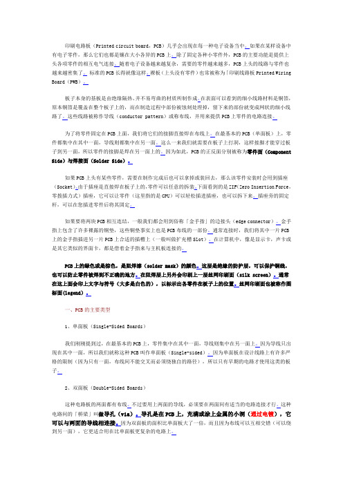
印刷电路板(Printed circuit board,PCB)几乎会出现在每一种电子设备当中。
如果在某样设备中有电子零件,那么它们也都是镶在大小各异的PCB上。
除了固定各种小零件外,PCB的主要功能是提供上头各项零件的相互电气连接。
随着电子设备越来越复杂,需要的零件越来越多,PCB上头的线路与零件也越来越密集了。
标准的PCB长得就像这样。
裸板(上头没有零件)也常被称为「印刷线路板Printed Wiring Board(PWB)。
板子本身的基板是由绝缘隔热、并不易弯曲的材质所制作成。
在表面可以看到的细小线路材料是铜箔,原本铜箔是覆盖在整个板子上的,而在制造过程中部份被蚀刻处理掉,留下来的部份就变成网状的细小线路了。
这些线路被称作导线(conductor pattern)或称布线,并用来提供PCB上零件的电路连接。
为了将零件固定在PCB上面,我们将它们的接脚直接焊在布线上。
在最基本的PCB(单面板)上,零件都集中在其中一面,导线则都集中在另一面。
这么一来我们就需要在板子上打洞,这样接脚才能穿过板子到另一面,所以零件的接脚是焊在另一面上的。
因为如此,PCB的正反面分别被称为零件面(Component Side)与焊接面(Solder Side)。
如果PCB上头有某些零件,需要在制作完成后也可以拿掉或装回去,那么该零件安装时会用到插座(Socket)。
由于插座是直接焊在板子上的,零件可以任意的拆装。
下面看到的是ZIF(Zero Insertion Force,零拨插力式)插座,它可以让零件(这里指的是CPU)可以轻松插进插座,也可以拆下来。
插座旁的固定杆,可以在您插进零件后将其固定。
如果要将两块PCB相互连结,一般我们都会用到俗称「金手指」的边接头(edge connector)。
金手指上包含了许多裸露的铜垫,这些铜垫事实上也是PCB布线的一部份。
通常连接时,我们将其中一片PCB 上的金手指插进另一片PCB上合适的插槽上(一般叫做扩充槽Slot)。
软性印刷电路板详细讲解

软性印刷电路板详细讲解软性印刷电路板简介1. 软板(FLEXIBLE PRINTED CIRCUIT)简介以俱挠性之基材制成之印刷电路板具有体积小重量轻可做3D 立体组装及动态挠曲等优。
2. 基本材料2.1. 铜箔基材COPPER CLAD LAMINATE由铜箔+胶+基材组合而成亦有无胶基材亦即仅铜箔+基材其价格较高在目前应用上较少除非特殊需求。
2.1.1. 铜箔Copper Foil 在材料上区分为压延铜(ROLLED ANNEAL Copper Foil)及电解铜(ELECTRO DEPOSITED Copper Foil)两种在特性上来说压延铜之机械特性较佳有挠折性要求时大部分均选用压延铜厚度上则区分为1/2oz (0.7mil) 1oz 2oz 等三种一般均使用1oz。
2.1.2. 基材Substrate在材料上区分为PI (Polymide ) Film 及PET (Polyester) Pilm 两种PI 之价格较高但其耐燃性较佳PET 价格较低但不耐热因此若有焊接需求时大部分均选用PI 材质厚度上则区分为1mil 2mil 两种。
2.1.3. 胶Adhesive胶一般有Acrylic 胶及Expoxy 胶两种最常使用Expoxy 胶厚度上由0.4~1mil 均有一般使用1mil 胶厚2.2. 覆盖膜Coverlay覆盖膜由基材+胶组合而成其基材亦区分为PI 与PET 两种视铜箔基材之材质选用搭配之覆盖膜覆盖膜之胶亦与铜箔基材之胶相同厚度则由0.5~1.4mil。
2.3. 补强材料Stiffener软板上局部区域为了焊接零件或增加补强以便安装而另外压合上去之硬质材料。
2.3.1. 补强胶片区分为PI 及PET 两种材质2.3.2. FR4 为Expoxy 材质2.3.3. 树脂板一般称尿素板补强材料一般均以感压胶PRESSURE SENSITIVE ADHESIVE 与软板贴合但PI 补强胶片则均使用热熔胶(Thermosetting)压合。
ipc印制电路板
印制电路板(Printed Circuit Boards)IPC-M-105Rigid Printed Board Manual刚性印制板设计手册IPC-D-325A Documentation Requirements for Printed Boards 印制板设计文件图册要求IPC-PE-740A Troubleshooting for Printed Board Manufacture andAssembly印制板制造和组装的故障排除IPC-MB-380Guidelines for Molded Interconnection Devices模压互连器件导则IPC-D-326A Information Requirements for Manufacturing Printed CircuitBoards and Other Electronic Assemblies印制板制造和其它电子组装的信息要求规范IPC-6010 Series IPC-6010 Qualification and Performance SeriesIPC-6010印制电路板质量标准和性能规范系列手册IPC-6011Generic Performance Specification for Printed Boards印制板通用性能规范IPC-6012B Qualification and Performance Specification for Rigid PrintedBoards刚性板的合格和性能规范要求IPC-6015Qualification & Performance Specification for OrganicMultichip Module (MCM-L) Mounting and Interconnections有机多芯片模块(MCM-L)安装及互连结构的鉴定与性能规范IPC-6016Qualification & Performance Specification for High DensityInterconnect (HDI) Layers or Boards高密度互连(HDI)层或印制板的鉴定与性能规范IPC-6018A Microwave End Product Board Inspection and Tech微波成品印制板的检验和测试IPC-A-600G Acceptability of Printed Boards印制板验收条件IPC-QE-605A Printed Board Quality Evaluation Handbook印制板质量评价IPC-PWB-EV AL-CH Printed Circuit Board Defect Evaluation Chart印制板缺陷评估图表IPC-HM-860Specification for Multilayer Hybrid Circuits多层混合电路规范IPC-TF-870Qualification and Performance of Polymer Thick Film PrintedBoards聚合物厚膜印制板的鉴定与性能IPC-ML-960Qualification and Performance Specification for MassLamination Panels for Multilayer printed Boards多层印制板的鉴定与性能规范用预制内层在制板的鉴定与性能规范IPC-TR-481Results of Multilayer Tests Program Round Robin多层印制板联合试验计划结果IPC-TR-551Quality Assessment of Printed Boards Used for Mounting andInterconnecting Electronic Components用于电子元件安装与互连的印制板质量评价IPC-TR-579Round Robin Reliability Evaluation of Small Diameter PlatedThrough Holes in PCBs印制板中小直径镀覆孔可靠性评价联合试验IPC-4552Specification for Electroless Nickel/Immersion Gold(ENIG)Plating for Printed Circuit Boards印制电路板表面非电镀镍/沉金规范IPC-DR-572Drilling Guidelines for Printed Boards印制板钻孔导则IT-95080Improvements/Alternatives to Mechanical Drilling of PCBVias印制板通孔机加工方案的改进和优选手册IPC-NC-349Computer Numerical Control Formatting for Drillers andRouters钻床和铣床用计算机数字控制格式IPC-SM-839Pre & Post Solder Mask Application Cleaning Guidelines施加阻焊前及施加后清洗导则IPC-HDI-1High Density Interconnect Microvia TechnologyCompendium高密度(HDI)互连微通孔技术纲要IPC/JPCA-4104Specification for High Density Interconnect (HDI) andMicrovia Materials高密度互连(HDI)及微导通孔材料规范IPC-6016Qualification & Performance Specification for High DensityInterconnect (HDI) Layers or Boards高密度互连(HDI)层或印制板的鉴定与性能规范IPC/JPCA-6801IPC/JPCA Terms & Definitions, Test Methods, and DesignExamples for Build-Up/High Density Interconnection积层/高密度互连的术语和定义、试验方法与设计例IPC-DD-135Qualification Testing for Deposited Organic InterlayerDielectric Materials for Multichip Modules多芯片组件内层有机绝缘材料的鉴定试验IT-96060High Density PCB Microvia Evaluation (October Project),Phase I, Round 1高密度印制板微通孔评价指标手册, 第一期第一版IT-97071High Density PCB Microvia Evaluation, Phase I, Round 2高密度印制板微通孔评价指标手册, 第一期第二版IT-30101High Density PCB Microvia Evaluation, Phase I, Round 3高密度印制板微通孔评价指标手册, 第一期第三版IT-98123Microvia Manufacturing Technology Cost Analysis Report微通孔制作技术成本核算报告IPC-2141A Controlled Impedance Circuit Boards & High Speed LogicDesign控制阻抗电路板与高速逻辑设计IPC-2251Design Guide for the Packaging of High Speed ElectronicCircuits高速电子电路封装的设计指南IPC-2252Design Guide for RF/Microwave Circuit Boards射频/微波电路板设计指南IPC-4103Specification for Base Materials for High Speed/HighFrequency Applications高速高频用基材规范IPC-6018A Microwave End Product Board Inspection and Test微波成品印制板的检验和测试IPC-D-317A Design Guidelines for Electronic Packaging Utilizing HighSpeed Techniques采用高速技术电子封装设计导则IPC-M-102Flexible Circuits Compendium挠性电路纲要IPC-4202Flexible Base Dielectrics for Use in Flexible Printed Circuitry挠性印制线路用挠性绝缘基底材料IPC-4203Adhesive Coated Dielectric Films for Use as Cover Sheets forFlexible Printed Circuitry and Flexible Adhesive BondingFilms挠性印制线路覆盖层用涂粘接剂绝缘薄膜IPC-4204Flexible Metal-Clad Dielectrics for Use in Fabrication ofFlexible Printed Circuitry挠性金属箔去电应用于柔性电路组装IPC-6013A Qualification & Performance Specification for FlexiblePrinted Boards挠性印制板的鉴定与性能规范IPC/JPCA-6202IPC/JPCA Performance Guide Manual for Single- andDouble-Sided Flexible Printed Wiring BoardsIPC/JPCA单双面挠性印制板性能手册IPC-FA-251Guidelines for Assembly of Single- and Double-Sided FlexCircuits单面和双面挠性电路组装导则IPC-FC-234Composite Metallic Materials Specification for PrintedWiring Boards印制线路板复合金属材料规范IPC-M-107Standards for Printed Board Materials Manual 印制板材料标准手册IPC-MI-660Incoming Inspection of Raw Materials Manual 原材料接收检验手册IPC-4101A Specifications for Base Materials for Rigid and MultilayerPrinted Boards刚性及多层印制板用基材规范IPC-4121Guidelines for Selecting Core Construction for MultilayerPrinted Wiring Board Applications 多层印制板用芯板结构选择导则IPC-4562Metal Foil for Printed Wiring Applications印制线路用金属箔IPC-CF-148A Resin Coated Metal for Printed Boards印制板用涂树脂金属箔IPC-CF-152B Composite Metallic Materials Specification for PrintedWiring Boards印制线路板复合金属材料规范IPC-TR-482New Developments in Thin Copper Foils薄铜箔的新发展IPC-TR-484Results of IPC Copper Foil Ductility Round Robin StudyIPC铜箔延展性联合研究结果IPC-TR-485Results of Copper Foil Rupture Strength Test Round RobinStudy铜箔断裂强度试验联合研究结果IPC-4412Specification for Finished Fabric Woven from ”E” Glass forPrinted Boards“E”类精纺玻璃纤维层印制板技术规范IPC-4130Specification & Characterization Methods for Nonwoven "E"Glass MaterialsE 玻璃纤维非织布材料规范及性能确定方法IPC-4110Specification and Characterization Methods for NonwovenCellulose Based Paper for Printed Boards印制板用纤维纸规范及性能确定方法IPC-4411-A Specification and Characterization Methods for Non-WovenPara-Aramid Reinforcement聚芳基酰胺非织布规范及性能确定方法IPC-SG-141Specification for Finished Fabric Woven from "S" Glass forPrinted Boards印制板用经处理S玻璃纤维织物规范IPC-A-142Specification for Finished Fabric Woven from Aramid forPrinted Boards印制板用经处理聚芳酰胺纤维编织物规范IPC-QF-143Specification for Finished Fabric Woven from Quartz (PureFused Silica) for Printed Boards印制板用经处理石英(熔融纯氧化硅)纤维编织物规范IPC-2524PWB Fabrication Data Quality Rating System印制板制造数据质量定级体系IPC-9151A Printed Board Process, Capability, Quality and RelativeReliability Benchmark Test Standard and Database印制板工艺, 容量, 质量,可靠性试验标准和数据库IPC-9191General Guidelines for Implementation of Statistical ProcessControl (SPC)实施统计过程控制(SPC)的通用导则IPC-9199Statistical Process Control (SPC) Quality Rating统计分析控制IPC-9252Guidelines and Requirements for Electrical Testing ofUnpopulated Printed Boards未组装印制板电测试要求和指南IT-97061PWB Hole to Land Misregistration: Causes and Reliability印制线路板通孔与焊盘的错位: 原因和可靠性IT-98103Reliability of Misregistered and Landless InnerlayerInterconnects in Thick Panels多层板内部无焊盘层互连错位的可靠性IPC-MS-810Guidelines for High V olume Microsection大批量显微剖切导则IPC-QL-653A Certification of Facilities that Inspect/Test Printed Boards,Components & Materials印制板、元器件及材料检验试验设备的认证IPC-TR-483Dimensional Stability Testing of Thin Laminates-Report onPhase 1 & 2 International Round Robin Test薄层压板尺寸稳走性试----国际联合试验计划I阶段及II阶段报告IPC-TR-486Round Robin Study to Correlate IST & MicrosectioningEvaluations for Inner-Layer Separation内层分离的互连应力测试(IST)与显微剖切相关性联合研究。
第五章 印制电路板

5.5 其他种类电路板
5.5.1 金属夹层电路板 金属夹层电路板由于具有金属夹层,因此能提供良好的 能提供良好的 热传导性、机械强度与电防护特性 热传导性、机械强度与电防护特性,对高操作温度的电 子元器件封装是理想的基板材,但是它有重量与价格高、 导孔制作较为困难、镀膜厚度不均匀时易发生卷屈等缺 点,这使得金属夹层电路板在微电子工业中使用的程度 不如以树脂玻璃纤维为基材的印制电路板。
Zr2O
3
系 数
价格
E-玻璃 (%) S-玻璃 (%) D-玻璃 (%)
15~ 25 <0.01 0~2 —
0~6 10~ 12 0~2 —
8~13
— < 0.1 — —
5.8 4.5 2 3.9 5 3.7 8
1~5 5~10 10~ 20 30~ 40
<0.01 0.10 18~ 21 — — —
材料种类 环氧树脂 硅胶树脂 聚亚硫胺 BT树脂 苯并环丁 烯 铁氟隆 聚脂类 丙烯树脂 氨基甲酸 脂
玻璃转移温度 (℃) 100~175 <−20 >260 >275 >350 NA 175 114 —
热膨胀系数 (ppm/℃) >20 >200 50 50 35~36 70~120 36 135 —
5.4.3 PCB基板制作的新技术 基板制作的新技术
(1)薄和超薄铜箔的采用。 )薄和超薄铜箔的采用。 (2)小孔钻削技术。 )小孔钻削技术。 (3)小孔金属化技术。 )小孔金属化技术。 (4)深孔电镀技术。 )深孔电镀技术。 (5)精细线条的图形刻蚀技术。 )精细线条的图形刻蚀技术。 (6)真空层压技术。 )真空层压技术。 (7)先进的表面涂复处理技术。 )先进的表面涂复处理技术。
- 1、下载文档前请自行甄别文档内容的完整性,平台不提供额外的编辑、内容补充、找答案等附加服务。
- 2、"仅部分预览"的文档,不可在线预览部分如存在完整性等问题,可反馈申请退款(可完整预览的文档不适用该条件!)。
- 3、如文档侵犯您的权益,请联系客服反馈,我们会尽快为您处理(人工客服工作时间:9:00-18:30)。
【印制电路板电镀及层压化学类简易实用手册】印制电路板制造技术的飞速发展,促使广大从事印制电路板制造行业的人们,加快知识更新。
为此,就必须掌握必要的新知识并与原有实用的科技成为工作必备的参考资料,更好地从事各种类型的科研工作。
这本手册就是使从事高科技行业新生产者尽快地掌握与印制电路板制造技术相关的知识,更好的理解和应用印制电路板制造方面的所涉及到的实用技术基础知识,为全面掌握印制电路板制造的全过程和所涉及到科学试验提供必要的基础知识和手段。
第一章溶液浓度计算方法在印制电路板制造技术,电镀为其中十分重要的一个环节,各种溶液占了很大的比重,对印制电路板的最终产品质量起到关键的作用。
无论是选购或者自配都必须进行科学计算。
正确的计算才能确保各种溶液的成分在工艺范围内,对确保产品质量起到重要的作用。
根据印制电路板生产的特点,提供六种计算方法供选用。
1.体积比例浓度计算:∙定义:是指溶质(或浓溶液)体积与溶剂体积之比值。
∙举例:1:5硫酸溶液就是一体积浓硫酸与五体积水配制而成。
2.克升浓度计算:∙定义:一升溶液里所含溶质的克数。
∙举例:100克硫酸铜溶于水溶液10升,问一升浓度是多少?100/10=10克/升3.重量百分比浓度计算(1)定义:用溶质的重量占全部溶液重理的百分比表示。
(2)举例:试求3克碳酸钠溶解在100克水中所得溶质重量百分比浓度?4.克分子浓度计算∙定义:一升中含1克分子溶质的克分子数表示。
符号:M、n表示溶质的克分子数、V表示溶液的体积。
如:1升中含1克分子溶质的溶液,它的克分子浓度为1M;含1/10克分子浓度为0.1M,依次类推。
∙举例:将100克氢氧化钠用水溶解,配成500毫升溶液,问这种溶液的克分子浓度是多少?解:首先求出氢氧化钠的克分子数:5. 当量浓度计算∙定义:一升溶液中所含溶质的克当量数。
符号:N(克当量/升)。
∙当量的意义:化合价:反映元素当量的内在联系互相化合所得失电子数或共同的电子对数。
这完全属于自然规律。
它们之间如化合价、原子量和元素的当量构成相表关系。
元素=原子量/化合价∙举例:钠的当量=23/1=23;铁的当量=55.9/3=18.6∙酸、碱、盐的当量计算法:A 酸的当量=酸的分子量/酸分子中被金属置换的氢原子数B 碱的当量=碱的分子量/碱分子中所含氢氧根数C 盐的当量=盐的分子量/盐分子中金属原子数金属价数6.比重计算∙定义:物体单位体积所有的重量(单位:克/厘米3)。
∙测定方法:比重计。
∙举例:A.求出100毫升比重为1.42含量为69%的浓硝酸溶液中含硝酸的克数?解:由比重得知1毫升浓硝酸重1.42克;在1.42克中69%是硝酸的重量,因此1毫升浓硝酸中硝酸的重量=1.42×(60/100)=0.98(克)∙B.设需配制25克/升硫酸溶液50升,问应量取比量1.84含量为98%硫酸多少体积?解:设需配制的50升溶液中硫酸的重量为W,则W=25克/升50=1250克由比重和百分浓度所知,1毫升浓硫酸中硫酸的重量为:1.84×(98/100)=18(克);则应量取浓硫酸的体积1250/18=69.4(毫升)∙波美度与比重换算方法:A.波美度= 144.3-(144.3/比重); B=144.3/(144.3-波美度)第二章电镀常用的计算方法在电镀过程中,涉及到很多参数的计算如电镀的厚度、电镀时间、电流密度、电流效率的计算。
当然电镀面积计算也是非常重要的,为了能确保印制电路板表面与孔内镀层的均匀性和一致性,必须比较精确的计算所有的被镀面积。
目前所采用的面积积分仪(对底片的板面积进行计算)和计算机计算软件的开发,使印制电路板表面与孔内面积更加精确。
但有时还必须采用手工计算方法,下例公式就用得上。
1.镀层厚度的计算公式:(厚度代号:d、单位:微米)d=(C×D k×t×ηk)/60r2.电镀时间计算公式:(时间代号:t、单位:分钟)t=(60×r×d)/(C×D k×ηk)3.阴极电流密度计算公式:(代号:、单位:安/分米2)ηk=(60×r×d)/(C×t×Dk)4.阴极电流以效率计算公式:Dk=(60×r×d)/(C×t×Dk)第三章沉铜质量控制方法化学镀铜(Electroless Plating Copper)俗称沉铜。
印制电路板孔金属化技术是印制电路板制造技术的关键之一。
严格控制孔金属化质量是确保最终产品质量的前提,而控制沉铜层的质量却是关键。
日常用的试验控制方法如下:1.化学沉铜速率的测定:使用化学沉铜镀液,对沉铜速率有一定的技术要求。
速率太慢就有可能引起孔壁产生空洞或针孔;而沉铜速率太快,将产生镀层粗糙。
为此,科学的测定沉铜速率是控制沉铜质量的手段之一。
以先灵提供的化学镀薄铜为例,简介沉铜速率测定方法:(1)材料:采用蚀铜后的环氧基材,尺寸为100×100(mm)。
(2)测定步骤:A. 将试样在120-140℃烘1小时,然后使用分析天平称重W1(g);B. 在350-370克/升铬酐和208-228毫升/升硫酸混合液(温度65℃)中腐蚀10分钟,清水洗净;C.在除铬的废液中处理(温度30-40℃)3-5分钟,洗干净;D. 按工艺条件规定进行预浸、活化、还原液中处理;E. 在沉铜液中(温度25℃)沉铜半小时,清洗干净;F. 试件在120-140℃烘1小时至恒重,称重W2(g)。
(3) 沉铜速率计算:速率=(W2-W1)104/8.93×10×10×0.5×2(μm)(4) 比较与判断:把测定的结果与工艺资料提供的数据进行比较和判断。
2.蚀刻液蚀刻速率测定方法通孔镀前,对铜箔进行微蚀处理,使微观粗化,以增加与沉铜层的结合力。
为确保蚀刻液的稳定性和对铜箔蚀刻的均匀性,需进行蚀刻速率的测定,以确保在工艺规定的范围内。
(1)材料:0.3mm覆铜箔板,除油、刷板,并切成100×100(mm);(2)测定程序:A.试样在双氧水(80-100克/升)和硫酸(160-210克/升)、温度30℃腐蚀2分钟,清洗、去离子水清洗干净;B.在120-140℃烘1小时,恒重后称重W2(g),试样在腐蚀前也按此条件恒重称重W1(g)。
(3)蚀刻速率计算速率=(W1-W2)104/2×8.933T(μm/min)式中:s-试样面积(cm2) T-蚀刻时间(min)(4)判断:1-2μm/min腐蚀速率为宜。
(1.5-5分钟蚀铜270-540mg)。
3.玻璃布试验方法在孔金属化过程中,活化、沉铜是化学镀的关键工序。
尽管定性、定量分析离子钯和还原液可以反映活化还原性能,但可靠性比不上玻璃布试验。
在玻璃布沉铜条件最苛刻,最能显示活化、还原及沉铜液的性能。
现简介如下:(1)材料:将玻璃布在10%氢氧化钠溶液里进行脱浆处理。
并剪成50×50(mm),四周末端除去一些玻璃丝,使玻璃丝散开。
(2)试验步骤:A.将试样按沉铜工艺程序进行处理;B. 置入沉铜液中,10秒钟后玻璃布端头应沉铜完全,呈黑色或黑褐色,2分钟后全部沉上,3分钟后铜色加深;对沉厚铜,10秒钟后玻璃布端头必须沉铜完全,30-40秒后,全部沉上铜。
C.判断:如达到以上沉铜效果,说明活化、还原及沉铜性能好,反则差。
第四章半固化片质量检测方法预浸渍材料是由树脂和载体构成的的一种片状材料。
其中树脂处于B-阶段,温度和压力作用下,具有流动性并能迅速地固化和完成粘结过程,并与载体一起构成绝缘层。
俗称半固化片或粘结片。
为确保多层印制电路板的高可靠性及质量的稳定性,必须对半固片特性进行质量检测(试层压法)。
半固化片特性包含层压前的特性和层压后特性两部分。
层压前的特性主要指:树脂含量%、流动性%、挥发物含量%和凝胶时间(S)。
层压后的特性是指:电气性能、热冲击性能和可燃性等。
为此,为确保多层印制电路板的高可靠姓和层压工艺参数的稳定性,检测层压前半固化片的特性是非常重要的。
1.树脂含量(%)测定:(1)试片的制作:按半固化片纤维方向:以45°角切成100×100(mm)小试块;(2)称重:使用精确度为0.001克天平称重W l(克);(3)加热:在温度为566.14℃加热烧60分钟,冷却后再进行称量W2(克);(4)计算: W1-W2树脂含量(%)=(W1-W2) /W1×1002. 树脂流量(%)测定:(1)试片制作:按半固化片纤维方向,以45°角切成100×100(mm)数块约20克试片;(2)称重:使用精确度为0.001克天平准确称重W1(克);(3)加热加压:按压床加热板的温度调整到171±3℃,当试片置入加热板内,施加压力为14±2Kg/cm2以上,加热加压5分钟,将流出胶切除并进行称量W2(克);(4)计算:树脂流量(%)=(W1-W2) /W1×1003. 凝胶时间测定:(1)试片制作:按半固化片纤维方向,以45°角切成50×50(mm)数块(每块约15克);(2)加热加压:调整加热板温度为171±3℃、压力为35Kg/cm2加压时间15秒;(3)测定:试片从加压开始时间到固化时间至是测定的结果。
4.挥发物含量侧定:(1)试片制作:按半固化片纤维方向,以45°角切成100×100(mm)1块;(2)称量:使用精确度为0.001克天平称重W1(克);(3)加热:使用空气循环式恒温槽,在163±3℃加热15分钟然后再用天平称重W2(克);(4)计算:挥发分(%)=(W1-W2) /W1×100第五章常见电性与特性名称解释在印制电路板制造技术方面,涉及到的很多专用名词和金属性能,其中包括物理、化学.机械等。
现只介绍常用的有关电气与物理,机械性能和相关方面的专用名词解释。
1.金属的物理性质:见表1:印制电路板制造常用金属物理性质数据表。
2.印制电路板制造常用盐类的金属含量:见表2:常用盐类金属含量数据表。
3.常用金属电化当量(见表3:电化当量数据表)4.一微米厚度镀层重量数据表(见表4)5.专用名词解释:(1)镀层硬度:是指镀层对外力所引起的局部表面变形的抵抗强度。
(2)镀层内应力:电镀后,镀层产生的内应力使阴极薄片向阳极弯曲(张应力)或背向阳极弯曲(压应力)。
(3)镀层延展性:金属或其它材料受到外力作用不发生裂纹所表现的弹性或塑性形变的能力称之。
(4)镀层可焊性:在一定条件下,镀层易于被熔融焊料所润湿的特性。