STM32模拟iic驱动eeprom24c128
STM32之EEPROM驱动
STM32之EEPROM驱动本⽂介绍如何使⽤STM32标准外设库驱动EEPROM,本例程驱动的EEPROM为AT24C02,通讯协议为IIC,使⽤IO⼝模拟⽅式。
本⽂适合对单⽚机及C语⾔有⼀定基础的开发⼈员阅读,MCU使⽤STM32F103VE系列。
1. EEPROM简介EEPROM全称为EEPROM(Electrically Erasable Programmable Read Only Memory)是电可擦除可编程只读存储器。
虽然名称为只读存储器,但是擦除和写⼊都是直接使⽤电路控制,不需要再使⽤外部设备来擦写,即设备在运⾏过程中即可随时擦除和写⼊。
可以按字节为单位修改数据,⽆需整个芯⽚擦除,且掉电后数据不丢失,⼀般⽤来存储⼀些配置信息,以便系统重新上电的时候加载。
2. 常⽤EEPROM⼀般常⽤的EEPROM为ATMEL公司(已被Microchip收购)的AT24Cxx系列,常⽤容量从1K到64Kbit不等,换算成字节为128到8K Bytes,可以根据项⽬需求和价格综合考虑选型。
3. EEPROM操作说明AT24C02容量为2Kbit,即256Byte,地址范围为0~255,即0~0xFF,使⽤1个字节即可表⽰,因此地址长度为1字节。
3.1. 通讯⽅式IAT24C02使⽤IIC协议跟MCU通讯。
3.2. 设备地址如果仅接⼊⼀个AT24C02,可以将设备的A0、A1、A2引脚全部接⼊低电平,那么此时该设备的地位为0x50,再增加⼀位读写标志位,最终读取操作时地址为0xA1,写⼊操作时地址为0xA0。
3.3. 读取数据读取当前字节:MCU直接发起读操作,设备返回当前字节,当前字节⾃动加1,该操作较少使⽤。
读取指定地址⼀个字节:MCU先向AT24C02写⼊⼀个地址,然后再发起⼀个读操作,AT24C02返回该地址存储的字节。
连续读取:MCU发起读当前字节,或者读指定地址字节,设备返回数据,MCU发送ACK,设备继续返回后续地址数据,直到MCU发送NACK,设备不再返回数据。
基于STM32的IIC_EEPROM案例说明
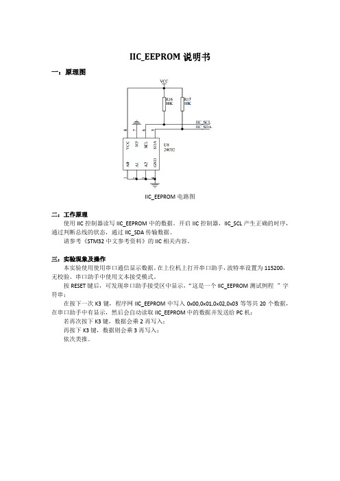
IIC_EEPROM说明书
一:原理图
IIC_EEPROM电路图
二:工作原理
使用IIC控制器读写IIC_EEPROM中的数据。
开启IIC控制器,IIC_SCL产生正确的时序,通过判断总线的状态,通过IIC_SDA传输数据。
请参考《STM32中文参考资料》的IIC相关内容。
三:实验现象及操作
本实验使用使用串口通信显示数据。
在上位机上打开串口助手,波特率设置为115200,无校验。
串口助手中使用文本接受模式。
按RESET键后,可发现串口助手接受区中显示,“这是一个IIC_EEPROM测试例程”字符串;
在按下一次K3键,程序网IIC_EEPROM中写入0x00,0x01,0x02,0x03等等共20个数据,在串口助手中有显示,然后会自动读取IIC_EEPROM中的数据并发送给PC机;
若再次按下K3键,数据会乘2再写入;
再按下K3键,数据则会乘3再写入;
依次类推。
单片机模拟I2C总线读写EEPROM(24CXX)程序一

单片机模拟I2C总线读写EEPROM(24CXX)程序一下面是一个最简单的读写程序,可以用来检测线路状况。
先附上程序和电路,后面附有说明。
电路:说明:P2 口的LED 都是我用来检测电路执行到哪一步的,个人觉得一目了然。
程序:#include #define unit unsigned int#define uchar unsigned charint ok;sbit scl=P0;sbit sda=P0;sb it led0=P2;sbit led1=P2;sb it led2=P2 ;sbit led3=P2;sb it led4=P2;sb it led5=P2 ;sbit led6=P2;sb it led7=P2;delay(void) //delay{ int i; led1=1; for(i=0;istart(void) //start{ sda=1; scl=1; delay(); sda=0; delay(); scl=0; led0=0;}stop(void) //stop{ sda=0; scl=1; delay(); sda=1; delay(); scl=0;}checkanswer(void) //check answer{ sda=1; scl=1; if(sda==1) { F0=1; led7=0; } scl=0; led3=0;}sendabyte(int temps) //send a byte{ uchar n=8; while(n--) { led2=1; if((temps&0x80)==0x80){ sda=1; scl=1; delay(); scl=0;}else{ sda=0; scl=1; delay(); scl=0;}temps=tempsreciveabyte() //recive a byte{ uchar n=8,tempr; while(n--) {//uchar idata *abyte scl=1;tempr=temprmain(void) //MAIN{start();sendabyte(0xa0);checkanswer();if(F0==1) return;sendabyte(0x00);checkanswer();if(F0==1) return;sendabyte(0x11);checkanswer();if(F0==1) return;/*-----------------------*/start(); sendabyte(0xa0);checkanswer();if(F0==1) return;。
STM32模拟iic驱动eeprom24c128
STM32模拟iic驱动eeprom24c128void IIC_Init(void) //IIC初始化函数{GPIO_InitTypeDef GPIO_InitStructure;RCC_APB2PeriphClockCmd(RCC_APB2Periph_GPIOE, ENABLE);//使能GPIOB时钟GPIO_InitStructure.GPIO_Pin = GPIO_Pin_2|GPIO_Pin_3;GPIO_InitStructure.GPIO_Mode = GPIO_Mode_Out_PP; //推挽输出GPIO_InitStructure.GPIO_Speed = GPIO_Speed_50MHz;GPIO_Init(GPIOE, &GPIO_InitStructure);GPIO_SetBits(GPIOE,GPIO_Pin_2|GPIO_Pin_3); //PE2,PE3 输出高}void IIC_Start(void) //IIC开始函数{SDA_OUT(); //sda线输出IIC_SDA=1;IIC_SCL=1;delay_us(5);IIC_SDA=0;//START:when CLK is high,DATA change form high to lowdelay_us(5);IIC_SCL=0; //钳住I2C总线,准备发送或接收数据}void IIC_Stop(void) //IIC停止函数{SDA_OUT();//sda线输出IIC_SCL=0;IIC_SDA=0;//STOP:when CLK is high DATA change form low to highdelay_us(5);IIC_SCL=1;IIC_SDA=1;//发送I2C总线结束信号delay_us(5);}u8 IIC_Wait_Ack(void) //等待应答{u8 ucErrTime=0;SDA_IN(); //SDA设置为输入IIC_SDA=1;delay_us(5);IIC_SCL=1;delay_us(1);while(READ_SDA){ucErrTime++;if(ucErrTime>250){IIC_Stop();return 1;}}IIC_SCL=0;//时钟输出0return 0;}void IIC_Ack(void) //SDA输出低电平,IIC应答{IIC_SCL=0;SDA_OUT();IIC_SDA=0;delay_us(2);IIC_SCL=1;delay_us(4);IIC_SCL=0;}void IIC_NAck(void) //SDA输出高电平,IIC非应答{IIC_SCL=0;SDA_OUT();IIC_SDA=1;delay_us(2);IIC_SCL=1;delay_us(4);IIC_SCL=0;}void IIC_Send_Byte(u8 txd) //IIC发送一个字节{u8 t;SDA_OUT(); //数据线输出模式IIC_SCL=0; //拉低时钟开始数据传输for(t=0;t<8;t++){IIC_SDA=(txd&0x80)>>7;txd<<=1;delay_us(5); //对TEA5767这三个延时都是必须的IIC_SCL=1;delay_us(5);IIC_SCL=0;delay_us(5);}}u8 IIC_Read_Byte(unsigned char ack) //IIC读取一个字节{unsigned char i,receive=0;SDA_IN();//SDA设置为输入for(i=0;i<8;i++ ){IIC_SCL=0;delay_us(5);IIC_SCL=1;receive<<=1;if(READ_SDA){receive++;}delay_us(5);}if (!ack)IIC_NAck();//发送nACKelseIIC_Ack(); //发送ACKreturn receive;}void AT24CXX_Init(void) //AT254C128初始化{IIC_Init();}u8 AT24CXX_ReadOneByte(u16 ReadAddr) //AT24C128读取一个字节{u8 temp=0;IIC_Start();IIC_Send_Byte(0XA0); //发送写命令IIC_Wait_Ack();IIC_Send_Byte(ReadAddr>>8);//发送高地址IIC_Wait_Ack();IIC_Send_Byte(ReadAddr%256); //发送低地址IIC_Wait_Ack();IIC_Start();IIC_Send_Byte(0XA1); //进入接收模式IIC_Wait_Ack();temp=IIC_Read_Byte(0);IIC_Stop(); //产生一个停止条件return temp;}void AT24CXX_WriteOneByte(u16 WriteAddr,u8 DataToWrite) {IIC_Start();IIC_Send_Byte(0XA0); //发送写命令IIC_Wait_Ack();IIC_Send_Byte(WriteAddr>>8);//发送高地址IIC_Wait_Ack();IIC_Send_Byte(WriteAddr%256); //发送低地址IIC_Wait_Ack();IIC_Send_Byte(DataToWrite); //发送字节IIC_Wait_Ack();IIC_Stop();//产生一个停止条件delay_ms(20);}u8 AT24CXX_Check(void){u8 temp;temp=AT24CXX_ReadOneByte(12333);//避免每次开机都写AT24CXXif(temp==0X55){return 0;}else//排除第一次初始化的情况{AT24CXX_WriteOneByte(12333,0X55);temp=AT24CXX_ReadOneByte(12333);if(temp==0X55){return 0;}}return 1;}void AT24CXX_Read(u16 ReadAddr,u8 *pBuffer,u16 NumToRead) {while(NumToRead){*pBuffer++=AT24CXX_ReadOneByte(ReadAddr++);NumToRead--;}}void AT24CXX_Write(u16 WriteAddr,u8 *pBuffer,u16 NumToWrite) {while(NumToWrite--){AT24CXX_WriteOneByte(WriteAddr,*pBuffer);WriteAddr++;pBuffer++;}}BY MaiLaoDie。
STM32 读写 EEPROM 24C02方法
函数功能:写入 24C02 EEPROM 的内部数据 参数:I2Cx,选定 STM32 的 I2C 接口,x 可以是 1 或 2
Address,24C02 的地址 Subaddress,EEPROM 读取的数据地址 s,为存放连续读取的数据缓冲数组 number,为读取连续数据的长度 注意:使用前确保总线已经结束 ------------------------------------------------------------*/ void EEPROM_24C02_Write(I2C_TypeDef* I2Cx, uint8_t Address, uint8_t Subaddress, vu8 *s, vu8 number) { //启动总线 I2C_GenerateSTART(I2Cx, ENABLE);
//Test on EV6 and clear it while(!I2C_CheckEvent(I2Cx, I2C_EVENT_MASTER_TRANSMITTER_MODE_SELECTED));
//In the case of a single data transfer disable ACK before reading the data I2C_AcknowledgeConfig(I2Cx, DISABLE);
while((number - 1) > 0) {
number--;
//Read a byte from the EEPROM *s = I2C_ReceiveData(I2Cx);
stm32Flash模拟eeprom心得(精品)

stm32Flash模拟eeprom心得(精品)STM32F10某FLASH模拟EEPROM心得花了几天时间研究tm32用Flah模拟EEPROM的问题,终于彻底弄懂了这种机制,由于我英文很菜,所以官方文档没有仔细看,而是直接去抠官方给出的例子程序,当然这种方法比较笨,但最终效果是一样的。
下面仅将我学习过程中的一些心得体会给大家介绍一下,希望能对需要的人有所帮助,有不足之处望大家积极指正。
首先推荐大家看的文档就是ST的官方文档《AN2594.pdf》和前辈总结出的《STM32FLASH模拟EEPROM使用和优化.pdf》和已经优化过的例程代码《FW_V3.1.0优化(FLASH模拟EEPROM).rar》下面开始进入主题1.为什么要用flah模拟eeprom?在许多应用场合下需要用eeprom保存非易失性的数据,但是意法半导体为了控制成本,没有在STM32F10某系列芯片中集成EEPROM,所以我们就需要用其内部集成的FLASH通过软件模拟EEPROM来达到同样的效果。
2.tm32中的片上FLASH特点根据《STM32F10某闪存编程》中的介绍,以小容量为例(如下图),我们要使用的是32个1K字节/页的主存储空间,也就是说这段空间里除了保存用户代码的部分,其余部分我们是可以利用其作为数据存储使用的。
tm32的FLASH分为主存储块和信息块。
主存储块用于保存具体的程序代码和用户数据,信息块用于负责由tm32出厂是放置2KB的启动程序(Bootloader)并锁死,用户无法更改。
选项字节存储芯片的配置信息及对主存储块的保护信息。
STM32的FLASH主存储块按页组织,有的产品每页1KB,有的产品每页2KB。
页面典型的用途就是用于按页擦除FLASH。
从这点来看,页面有点像通用FLASH的扇区上图中FLASH一页大小为1KB。
范围为从地址0某08000000开始的32KB内。
对Flah的写入操作要“先擦除后写入”的原则;闪存的读写涉及一个概念,字(Word)32bit和半字(HalfWord)16bit,虽然STM32FLASH也是由字节组成,但STM32FLASH的编程每次都是以16bit半字为单位,且FLASH地址必须为偶数,否则会出错。
STM32的I2C-EEPROM已调试成功
STM32的I2C-EEPROM已调试成功万利的I2C-EEPROM例程有些问题,经本人两个昼夜的反复试验,已修改完善。
修改了两个地方,在void I2C_EE_BufferWrite(u8* pBuffer, u8 WriteAddr, u16 NumByteToWrite)写操作函数和void I2C_EE_BufferRead(u8* pBuffer, u8 ReadAddr, u16 NumByteToRead)读操作函数体内的开头先要执行一句I2C_EE_WaitEepromStandbyState();这样在以后调用写操作函数和读操作函数时就不用执行I2C_EE_WaitEepromStandbyState()了。
但上电复位后先要执行一次读操作,以后就可以无限制的随便调用这两个函数了。
详细如下。
/* Includes ------------------------------------------------------------------*/#include "stm32f10x_lib.h"#include "i2c_ee.h"#include"delay.h"/* Private typedef -----------------------------------------------------------*//* Private define ------------------------------------------------------------*/#define I2C_Speed 10000#define I2C1_SLAVE_ADDRESS7 0xA0#define I2C_PageSize 4/* Private macro -------------------------------------------------------------*//* Private variables ---------------------------------------------------------*/u16 EEPROM_ADDRESS;/* Private function prototypes -----------------------------------------------*/void I2C_Configuration(void);/************************************************************** ****************** Function Name : I2C_Configuration* Description : I2C Configuration* Input : None* Output : None* Return : None*************************************************************** ****************/void I2C_Configuration(void){GPIO_InitTypeDef GPIO_InitStructure;I2C_InitTypeDef I2C_InitStructure;/* Configure I2C1 pins: SCL and SDA */GPIO_InitStructure.GPIO_Pin = GPIO_Pin_6 | GPIO_Pin_7;GPIO_InitStructure.GPIO_Speed = GPIO_Speed_10MHz;GPIO_InitStructure.GPIO_Mode = GPIO_Mode_AF_OD;//开漏输出GPIO_Init(GPIOB, &GPIO_InitStructure);/* I2C configuration */I2C_InitStructure.I2C_Mode = I2C_Mode_I2C;//设置 I2C为 I2C 模式I2C_InitStructure.I2C_DutyCycle = I2C_DutyCycle_2;//I2C快速模式 Tlow / Thigh = 2I2C_InitStructure.I2C_OwnAddress1 = I2C1_SLAVE_ADDRESS7;//设置第一个设备地址I2C_InitStructure.I2C_Ack = I2C_Ack_Enable;//使能应答I2C_InitStructure.I2C_AcknowledgedAddress = I2C_AcknowledgedAddress_7bit;//应答 7位地址I2C_InitStructure.I2C_ClockSpeed = I2C_Speed;//设置时钟频率/* I2C Peripheral Enable */I2C_Cmd(I2C1, ENABLE);//使能I2C外设/* Apply I2C configuration after enabling it */I2C_Init(I2C1, &I2C_InitStructure);}/************************************************************** ****************** Function Name : I2C_EE_Init* Description : Initializes peripherals used by the I2C EEPROM driver.* Input : None* Output : None* Return : None*************************************************************** ****************/void I2C_EE_Init(){/* I2C configuration */I2C_Configuration();/* depending on the EEPROM Address selected in thei2c_ee.h file */#ifdef EEPROM_Block0_ADDRESS/* Select the EEPROM Block0 to write on */EEPROM_ADDRESS = EEPROM_Block0_ADDRESS;#endif#ifdef EEPROM_Block1_ADDRESS/* Select the EEPROM Block1 to write on */EEPROM_ADDRESS = EEPROM_Block1_ADDRESS;#endif#ifdef EEPROM_Block2_ADDRESS/* Select the EEPROM Block2 to write on */EEPROM_ADDRESS = EEPROM_Block2_ADDRESS;#endif#ifdef EEPROM_Block3_ADDRESS/* Select the EEPROM Block3 to write on */EEPROM_ADDRESS = EEPROM_Block3_ADDRESS;#endif}/************************************************************** ****************** Function Name : I2C_EE_BufferWrite* Description : Writes buffer of data to the I2C EEPROM.* Input : - pBuffer : pointer to the buffer containing the data to be* written to the EEPROM.* - WriteAddr : EEPROM's internal address to write to.* - NumByteToWrite : number of bytes to write to the EEPROM.* Output : None* Return : NonepBuffer:指向要写入数据数组的指针WriteAddr:24c02中要写入数据的首地址NumByteToWrite:写入的字节数*************************************************************** ****************/void I2C_EE_BufferWrite(u8* pBuffer, u8 WriteAddr, u16 NumByteToWrite)//将缓冲器的数据写入EEPROM{u8 NumOfPage = 0, NumOfSingle = 0, Addr = 0, count = 0;Addr = WriteAddr % I2C_PageSize;//写入地址是每页的第几位count = I2C_PageSize - Addr;//在开始的一页要写入的个数NumOfPage = NumByteT oWrite / I2C_PageSize;//要写入的页数NumOfSingle = NumByteToWrite % I2C_PageSize;//不足一页的个数I2C_EE_WaitEepromStandbyState();//EEPROM设为待命状态/* If WriteAddr is I2C_PageSize aligned */if(Addr == 0) //写入地址是页的开始{/* If NumByteToWrite < I2C_PageSize */if(NumOfPage == 0) //数据小于一页{I2C_EE_PageWrite(pBuffer, WriteAddr, NumOfSingle);//写少于一页的数据I2C_EE_WaitEepromStandbyState();//EEPROM设为待命状态}/* If NumByteToWrite > I2C_PageSize */else //数据大于等于一页{while(NumOfPage--)//要写入的页数{I2C_EE_PageWrite(pBuffer, WriteAddr, I2C_PageSize); //写一页的数据I2C_EE_WaitEepromStandbyState();//EEPROM设为待命状态WriteAddr += I2C_PageSize;pBuffer += I2C_PageSize;}if(NumOfSingle!=0)//剩余数据小于一页{I2C_EE_PageWrite(pBuffer, WriteAddr, NumOfSingle);//写少于一页的数据I2C_EE_WaitEepromStandbyState();//EEPROM设为待命状态}}}/* If WriteAddr is not I2C_PageSize aligned */else //写入地址不是页的开始{/* If NumByteToWrite < I2C_PageSize */if(NumOfPage== 0) //数据小于一页{I2C_EE_PageWrite(pBuffer, WriteAddr, NumOfSingle);//写少于一页的数据I2C_EE_WaitEepromStandbyState();//EEPROM设为待命状态}/* If NumByteToWrite > I2C_PageSize */else//数据大于等于一页{NumByteToWrite -= count;NumOfPage = NumByteT oWrite / I2C_PageSize; //重新计算要写入的页数NumOfSingle = NumByteToWrite % I2C_PageSize;//重新计算不足一页的个数if(count != 0)//在此处count一定不为0,此判断条件好象有点多余{I2C_EE_PageWrite(pBuffer, WriteAddr, count);//将开始的空间写满一页I2C_EE_WaitEepromStandbyState();//EEPROM设为待命状态WriteAddr += count;pBuffer += count;}while(NumOfPage--)//要写入的页数{I2C_EE_PageWrite(pBuffer, WriteAddr, I2C_PageSize);//写一页的数据I2C_EE_WaitEepromStandbyState();//EEPROM设为待命状态WriteAddr += I2C_PageSize;pBuffer += I2C_PageSize;}if(NumOfSingle != 0)//剩余数据小于一页{I2C_EE_PageWrite(pBuffer, WriteAddr, NumOfSingle); //写少于一页的数据I2C_EE_WaitEepromStandbyState();//EEPROM设为待命状态}}}}/************************************************************** ****************** Function Name : I2C_EE_ByteWrite* Description : Writes one byte to the I2C EEPROM.* Input : - pBuffer : pointer to the buffer containing the data to be* written to the EEPROM.* - WriteAddr : EEPROM's internal address to write to.* Output : None* Return : NonepBuffer:指向要写入数据数组的指针WriteAddr:24c02中要写入数据的首地址*************************************************************** ****************/void I2C_EE_ByteWrite(u8* pBuffer, u8 WriteAddr)//写一个字节到EEPROM{/* Send STRAT condition */I2C_GenerateSTART(I2C1, ENABLE);//产生 I2Cx传输 START条件/* Test on EV5 and clear it */while(!I2C_CheckEvent(I2C1,I2C_EVENT_MASTER_MODE_SELECT)); //检查最近一次I2C事件是否是输入的事件/* Send EEPROM address for write */I2C_Send7bitAddress(I2C1, EEPROM_ADDRESS, I2C_Direction_Transmitter);//向指定的从 I2C设备传送地址字,选择发送方向/* Test on EV6 and clear it */while(!I2C_CheckEvent(I2C1,I2C_EVENT_MASTER_TRANSMITTER_MODE_SELECTED));//检查最近一次 I2C事件是否是输入的事件/* Send the EEPROM's internal address to write to */I2C_SendData(I2C1, WriteAddr);//通过外设 I2Cx发送地址/* Test on EV8 and clear it */while(!I2C_CheckEvent(I2C1,I2C_EVENT_MASTER_BYTE_TRANSMITTED));//检查最近一次 I2C事件是否是输入的事件/* Send the byte to be written */I2C_SendData(I2C1, *pBuffer); //通过外设 I2Cx发送数据/* Test on EV8 and clear it */while(!I2C_CheckEvent(I2C1,I2C_EVENT_MASTER_BYTE_TRANSMITTED));//检查最近一次 I2C事件是否是输入的事件/* Send STOP condition */I2C_GenerateSTOP(I2C1, ENABLE);//产生 I2Cx传输 STOP条件}/************************************************************** ****************** Function Name : I2C_EE_PageWrite* Description : Writes more than one byte to the EEPROM with a single WRITE* cycle. The number of byte can't exceed the EEPROM page size.* Input : - pBuffer : pointer to the buffer containing the data to be* written to the EEPROM.* - WriteAddr : EEPROM's internal address to write to.* - NumByteToWrite : number of bytes to write to the EEPROM.* Output : None* Return : NonepBuffer:指向要写入数据数组的指针WriteAddr:24c02中要写入数据的首地址NumByteToWrite:写入的字节数*************************************************************** ****************/void I2C_EE_PageWrite(u8* pBuffer, u8 WriteAddr, u8 NumByteToWrite)//写少于一页的数据{/* Send START condition */I2C_GenerateSTART(I2C1, ENABLE);//产生 I2Cx传输 START条件/* Test on EV5 and clear it */while(!I2C_CheckEvent(I2C1,I2C_EVENT_MASTER_MODE_SELECT)); //检查最近一次I2C事件是否是输入的事件/* Send EEPROM address for write */I2C_Send7bitAddress(I2C1, EEPROM_ADDRESS, I2C_Direction_Transmitter);//向指定的从 I2C设备传送地址字,选择发送方向/* Test on EV6 and clear it */while(!I2C_CheckEvent(I2C1,I2C_EVENT_MASTER_TRANSMITTER_MODE_SELECTED)); //检查最近一次 I2C事件是否是输入的事件/* Send the EEPROM's internal address to write to */I2C_SendData(I2C1, WriteAddr); //通过外设 I2Cx发送地址/* Test on EV8 and clear it */while(! I2C_CheckEvent(I2C1, I2C_EVENT_MASTER_BYTE_TRANSMITTED)); //检查最近一次I2C 事件是否是输入的事件/* While there is data to be written */while(NumByteT oWrite--){/* Send the current byte */I2C_SendData(I2C1, *pBuffer); //通过外设 I2Cx发送数据/* Point to the next byte to be written */pBuffer++;/* Test on EV8 and clear it */while (!I2C_CheckEvent(I2C1, I2C_EVENT_MASTER_BYTE_TRANSMITTED));//检查最近一次 I2C事件是否是输入的事件}/* Send STOP condition */I2C_GenerateSTOP(I2C1, ENABLE);//产生 I2Cx传输 STOP条件}/************************************************************** ****************** Function Name : I2C_EE_BufferRead* Description : Reads a block of data from the EEPROM.* Input : - pBuffer : pointer to the buffer that receives the data read* from the EEPROM.* - ReadAddr : EEPROM's internal address to read from.* - NumByteT oRead : number of bytes to read from the EEPROM.* Output : None* Return : NonepBuffer:指向要保存读出数据的数组的指针ReadAddr:24c02中要读出数据的首地址NumByteToRead:读出的字节数*************************************************************** ****************/void I2C_EE_BufferRead(u8* pBuffer, u8 ReadAddr, u16 NumByteToRead)//将EEPROM的数据读入缓冲器{I2C_EE_WaitEepromStandbyState();//EEPROM设为待命状态/* Send START condition */I2C_GenerateSTART(I2C1, ENABLE);//产生 I2Cx传输 START条件/* Test on EV5 and clear it */while(!I2C_CheckEvent(I2C1,I2C_EVENT_MASTER_MODE_SELECT));//检查最近一次 I2C事件是否是输入的事件/* In the case of a single data transfer disable ACK before reading the data */if(NumByteToRead==1){I2C_AcknowledgeConfig(I2C1, DISABLE);//使能或者失能指定I2C的应答功能}/* Send EEPROM address for write */I2C_Send7bitAddress(I2C1, EEPROM_ADDRESS, I2C_Direction_Transmitter);//向指定的从 I2C设备传送地址字,选择发送方向/* Test on EV6 and clear it */while(!I2C_CheckEvent(I2C1,I2C_EVENT_MASTER_TRANSMITTER_MODE_SELECTED));//检查最近一次 I2C事件是否是输入的事件/* Clear EV6 by setting again the PE bit */I2C_Cmd(I2C1, ENABLE);//使能或者失能 I2C外设/* Send the EEPROM's internal address to write to */I2C_SendData(I2C1, ReadAddr); //通过外设 I2Cx发送地址/* Test on EV8 and clear it */while(!I2C_CheckEvent(I2C1,I2C_EVENT_MASTER_BYTE_TRANSMITTED));//检查最近一次 I2C事件是否是输入的事件/* Send STRAT condition a second time */I2C_GenerateSTART(I2C1, ENABLE);//产生 I2Cx传输 START条件/* Test on EV5 and clear it */while(!I2C_CheckEvent(I2C1,I2C_EVENT_MASTER_MODE_SELECT));//检查最近一次 I2C事件是否是输入的事件/* Send EEPROM address for read */I2C_Send7bitAddress(I2C1, EEPROM_ADDRESS, I2C_Direction_Receiver);//向指定的从I2C设备传送地址字,选择接收方向/* Test on EV6 and clear it */while(!I2C_CheckEvent(I2C1,I2C_EVENT_MASTER_RECEIVER_MODE_SELECTED));//检查最近一次 I2C事件是否是输入的事件/* While there is data to be read */while(NumByteT oRead){/* Test on EV7 and clear it */if(I2C_CheckEvent(I2C1,I2C_EVENT_MASTER_BYTE_RECEIVED)) //检查最近一次I2C事件是否是输入的事件{if(NumByteToRead == 2){/* Disable Acknowledgement */I2C_AcknowledgeConfig(I2C1, DISABLE);//使能或者失能指定I2C的应答功能}if(NumByteToRead == 1){/* Send STOP Condition */I2C_GenerateSTOP(I2C1, ENABLE);//产生 I2Cx传输 STOP条件}/* Read a byte from the EEPROM */*pBuffer = I2C_ReceiveData(I2C1);//返回通过 I2Cx最近接收的数据/* Point to the next location where the byte read will be saved */pBuffer++;/* Decrement the read bytes counter */NumByteToRead--;}}/* Enable Acknowledgement to be ready for another reception */I2C_AcknowledgeConfig(I2C1, ENABLE);//使能或者失能指定I2C的应答功能}/************************************************************** ****************** Function Name : I2C_EE_WaitEepromStandbyState* Description : Wait for EEPROM Standby state* Input : None* Output : None* Return : None*************************************************************** ****************/void I2C_EE_WaitEepromStandbyState(void) //EEPROM设为待命状态{vu16 SR1_Tmp = 0;do{/* Send START condition */I2C_GenerateSTART(I2C1, ENABLE);//产生 I2Cx传输 START条件/* Read I2C1 SR1 register */SR1_Tmp = I2C_ReadRegister(I2C1, I2C_Register_SR1);//读取指定的 I2C寄存器 I2C_SR1 并返回其值/* Send EEPROM address for write */I2C_Send7bitAddress(I2C1, EEPROM_ADDRESS, I2C_Direction_Transmitter);//向指定的从I2C设备传送地址字,选择发送方向}while(!(I2C_ReadRegister(I2C1, I2C_Register_SR1) & 0x0002));//地址发送结束/* Clear AF flag */I2C_ClearFlag(I2C1, I2C_FLAG_AF);//清除 I2Cx的应答错误标志位}。
STM32模拟EEPROM的使用和优化

((uint8_t)0x05)
uint16_t VirtAddVarTab[NumbOfVar] = {0, 1, 2}; //NumbOfVar 定义的比用的多实际是{0, 1, 2, 0, 0},虚拟地址 0 的数据换页后将出现旧数据覆盖最新数据
EE_WriteVariable(VirtAddVarTab[1], VarValue); temp=0; EE_ReadVariable(0, &temp);//不换页读出数据是对的,换页后读出数据错误 }
}
//====================================================================================
int main(void) { uint16_t temp;
for (VarValue = 0; VarValue < 100; VarValue++) {
EE_WriteVariable(VirtAddVarTab[0], VarValue); } for (VarValue = 0; VarValue < 50; VarValue++) {
} }
STM32 FLASH 模拟 EEPROM 使用注意: 不少人问该程序的 FLASH 保存数据多少和使用寿命 保存数据多少跟 FLASH 页大小有关,如果页大小是 1K 那么只能保存 1024/4-1=256-1 个 16 位数据,如果你保 存 8 位数,你可以 2 个 8 位数据组合后保存或者直接保存,如果保存 32 位数据那就拆成 2 个 16 位保存,当然 关于寿命 现在 STM32 的 FLASH 寿命是 10000 次, 如果你保存 255 个数据那么每次修改 1 个数据 FLASH 就要擦写 1 次,如果你保存 1 个数据,那么你修改 255 次该页才擦 1 次,继续用另外 1 页,建议保存数据个数不要超过 50%,当然如果你的数据基本都不修改你保存 255 个也是没有任何问题(你的数据都不修改根本不用关心寿命问题了:)。
stm32F103模拟I2C读写24c02

/*********文件名:i2c_ee.h**********//* Define to prevent recursive inclusion ------------------------------------ */#ifndef __I2C_EE_H#define __I2C_EE_H/* Includes ------------------------------------------------------------------*/#include "stm32f10x.h"/* Exported macro ------------------------------------------------------------*/#define ADDR_24CXX 0xA0#define SCLH GPIOB->BSRR = GPIO_Pin_6#define SCLL GPIOB->BRR = GPIO_Pin_6#define SDAH GPIOB->BSRR = GPIO_Pin_7#define SDAL GPIOB->BRR = GPIO_Pin_7#define SCLread GPIOB->IDR & GPIO_Pin_6#define SDAread GPIOB->IDR & GPIO_Pin_7/* Exported functions ------------------------------------------------------- */void I2C_EE_Init(void);uint8_t I2C_EE_BufferWrite(uint8_t *psrc_data,uint8_t adr,uint8_t nbyte); uint8_t I2C_EE_BufferRead(uint8_t *pdin_data,uint8_t adr,uint8_t nbyte);#endif /* __I2C_EE_H *//////////////////////////////////////////////////////////////////////////////////////////////////////////////////////////////////////////////////////////////////////////////////////////////////////////////////////////////////////////////////////////////////////////////////////////////////////////////////////////*********文件名:i2c_ee.c**********/#include "i2c_ee.h"enum ENUM_TWI_REPLY{TWI_NACK=0,TWI_ACK=1};enum ENUM_TWI_BUS_STATE{TWI_READY=0,TWI_BUS_BUSY=1,TWI_BUS_ERROR=2};void I2C_EE_Init(void){GPIO_InitTypeDef GPIO_InitStructure;RCC_APB2PeriphClockCmd(RCC_APB2Periph_GPIOB, ENABLE);// Configure I2C1 pins: SCL and SDAGPIO_InitStructure.GPIO_Pin = GPIO_Pin_6 | GPIO_Pin_7;GPIO_InitStructure.GPIO_Speed = GPIO_Speed_50MHz;GPIO_InitStructure.GPIO_Mode = GPIO_Mode_Out_OD;GPIO_Init(GPIOB, &GPIO_InitStructure);}void TWI_delay(void){uint8_t i=10; //i=10延时1.5us//这里可以优化速度,经测试最低到5还能写入while(i--);}/**************************************************************************延时ms:延时的毫秒数CYCLECOUNTER / 72000000***************************************************************************/void DelayMs(uint16_t ms){uint16_t iq0;uint16_t iq1;for(iq0 = ms; iq0 > 0; iq0--){for(iq1 = 11998; iq1 > 0; iq1--); // ( (6*iq1+9)*iq0+15 ) / 72000000}}uint8_t TWI_Start(void){SDAH;SCLH;TWI_delay();if(!SDAread)return TWI_BUS_BUSY; //SDA线为低电平则总线忙,退出SDAL;TWI_delay();if(SDAread) return TWI_BUS_ERROR; //SDA线为高电平则总线出错,退出 SCLL;TWI_delay();return TWI_READY;}/*void TWI_Stop(void){SCLL;TWI_delay();SDAL;SCLH;TWI_delay();SDAH;TWI_delay();}*/void TWI_Stop(void) {SDAL;SCLL;TWI_delay();SCLH;TWI_delay();SDAH;TWI_delay();}void TWI_Ack(void) {SCLL;TWI_delay();SDAL;TWI_delay();SCLH;TWI_delay();SCLL;TWI_delay();}void TWI_NoAck(void) {SCLL;TWI_delay();SDAH;TWI_delay();SCLH;SCLL;TWI_delay();}uint8_t TWI_WaitAck(void) //返回为:=1有ACK,=0无ACK {SCLL;TWI_delay();SDAH;TWI_delay();SCLH;TWI_delay();if(SDAread){SCLL;return 0;}SCLL;return 1;}void TWI_SendByte(uint8_t SendByte) //数据从高位到低位// {uint8_t i=8;while(i--){SCLL;TWI_delay();if(SendByte&0x80)SDAH;elseSDAL;SendByte<<=1;TWI_delay();SCLH;TWI_delay();}SCLL;}uint8_t TWI_ReceiveByte(void) //数据从高位到低位//{uint8_t i=8;uint8_t ReceiveByte=0;SDAH;while(i--){ReceiveByte <<= 1;SCLL;TWI_delay();SCLH;TWI_delay();if(SDAread){ReceiveByte |= 0x01;}}SCLL;return ReceiveByte;}//返回:3写入成功;0写器件地址出错,1总线忙,2出错//写入1字节数据SendByte:待写入数据WriteAddress:待写入地址uint8_t TWI_WriteByte(uint8_t SendByte, uint8_t WriteAddress){uint8_t i;uint16_t j;i = TWI_Start();if(i)return i;TWI_SendByte( ADDR_24CXX & 0xFE);//写器件地址写入:地址最低位是0,读取:地址最低位是1if(!TWI_WaitAck()){TWI_Stop();return 0;}TWI_SendByte(WriteAddress); //设置起始地址TWI_WaitAck();TWI_SendByte(SendByte); //写数据TWI_WaitAck();TWI_Stop();//注意:因为这里要等待EEPROM写完,可以采用查询或延时方式(10ms) DelayMs(12); //写入延时12ms 写周期大于10ms即可return 3;}//返回:0写器件地址出错,1总线忙,2出错,//读出1字节数据//ReadAddress:待读出地址uint8_t TWI_ReadByte( uint8_t ReadAddress){uint8_t i,temp;i = TWI_Start();if(i)return i;TWI_SendByte((ADDR_24CXX & 0xFE));//写器件地址,先执行一次伪写操作if(!TWI_WaitAck()){TWI_Stop();return 0;}TWI_SendByte(ReadAddress); //设置起始地址TWI_WaitAck();TWI_Start();TWI_SendByte((ADDR_24CXX & 0xFE)|0x01); //读器件地址写入:地址最低位是0,读取:地址最低位是1TWI_WaitAck();//*pDat = TWI_ReceiveByte();temp = TWI_ReceiveByte();TWI_NoAck();TWI_Stop();return temp;//返回的如果是0,1,2则与错误代码相同了,再考虑一下}/***************************************************************************向24c256中写多个字节psrc_data:指向要写入数据数组的指针adr:24c256中要写入数据的首地址nbyte:写入的字节数返回值: 0:执行完毕;1:执行出现错误形参中:C02只有一个地址adr;C256中有高位地址hadr和低位地址ladr***************************************************************************/uint8_t I2C_EE_BufferWrite(uint8_t *psrc_data,uint8_t adr,uint8_t nbyte){uint8_t i;for(;nbyte!=0;nbyte--){i = TWI_Start();if(i)return i;TWI_SendByte( ADDR_24CXX & 0xFE);//写器件地址if(!TWI_WaitAck()){TWI_Stop();return 0;}TWI_SendByte(adr); //设置起始地址TWI_WaitAck();TWI_SendByte(*psrc_data); //写数据TWI_WaitAck();psrc_data++; //指向待写数据的指针加1adr++; //对24C08的操作地址加1TWI_Stop();//注意:因为这里要等待EEPROM写完,可以采用查询或延时方式(10ms) DelayMs(12); //写入延时12ms 写周期大于10ms即可}return 0;}/***************************************************************************从24c02读多个字节pdin_data:指向要保存读出数据的数组的指针adr:24c02中要读出数据的首地址nbyte:读出的字节数返回值: 0:执行完毕;1:执行出现错误***************************************************************************/uint8_t I2C_EE_BufferRead(uint8_t *pdin_data,uint8_t adr,uint8_t nbyte) {uint8_t i;i = TWI_Start();if(i)return i;TWI_SendByte((ADDR_24CXX & 0xFE));//写器件地址,先执行一次伪写操作if(!TWI_WaitAck()){TWI_Stop();return 0;}TWI_SendByte(adr); //设置起始地址TWI_WaitAck();TWI_Start();TWI_SendByte((ADDR_24CXX & 0xFE)|0x01); //读器件地址写入:地址最低位是0,读取:地址最低位是1TWI_WaitAck();while(nbyte!=1) //读入前(nbyte-1)个字节{*pdin_data = TWI_ReceiveByte(); //循环从24C02中读数据,存入pdin_data所指的存储器中TWI_Ack(); //IIC应答pdin_data++; //指向存储读入数据的存储器指针加1nbyte--; //剩余要读入的字节减1};*pdin_data = TWI_ReceiveByte(); //读入最后一个字节TWI_NoAck(); //IIC无应答操作TWI_Stop();return 0;}/*void TWI_24CXX_Write(uint8_t* pDat, uint8_t nAddr, uint8_t nLen) {uint16_t i;for(i=0;i<nLen;i++){TWI_WriteByte(*(pDat+i), nAddr+i);}}void TWI_24CXX_Read(uint8_t* pDat, uint8_t nAddr, uint8_t nLen) {uint16_t i;for(i=0; i<nLen; i++)*(pDat+i) = TWI_ReadByte(nAddr+i);}*/。
STM32驱动AT24CXX系列芯片
STM32驱动AT24CXX系列芯片标签:stm32存储AT24CXX驱动2014-10-03 22:25 963人阅读评论(0) 收藏举报分类:设备驱动(29)版权声明:本文为博主原创文章,未经博主允许不得转载。
AT24Cxx系列EEPROM是由美国Mcrochip公司出品,1-512K位的支持I2C总线数据传送协议的串行CMOS E2PROM,可用电擦除,可编程自定时写周期(包括自动擦除时间不超过10ms,典型时间为5ms)的。
串行E2PROM一般具有两种写入方式,一种是字节写入方式,还有另一种页写入方式。
允许在一个写周期内同时对1个字节到一页的若干字节的编程写入,1页的大小取决于芯片内页寄存器的大小。
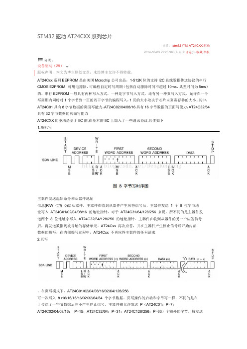
其中,AT24C01具有8字节数据的页面写能力,AT24C02/04/08/16具有16字节数据的页面写能力,AT24C32/64具有32字节数据的页面写能力AT24CXX的驱动是基于IIC的,在基本的IIC上加入了一些通讯协议,具体如下1.随机写主器件发送起始命令和从器件地址信息(R/W 位置0)给从器件,主器件在收到从器件产生应答信号后,主器件发送 1 个8 位字节地址写入AT24C01/02/04/08/16 的地址指针,对于AT24C31/64/128/256 来说,所不同的是主器件发送两个8 位地址字写入AT24C32/64/128/256 的地址指针。
主器件在收到从器件的另一个应答信号后,再发送数据到被寻址的存储单元。
AT24Cxx 再次应答,并在主器件产生停止信号后开始内部数据的擦写,在内部擦写过程中,AT24Cxx 不再应答主器件的任何请求2.页写。
在页写模式下,AT24C01/02/04/08/16/32/64/128/256可一次写入8 /16/16/16/16/32/32/64/64 个字节数据。
页写操作的启动和字节写一样,不同的是在于传送了一字节数据后并不产生停止信号。
STM32F0单片机用 I2C HAL 库读写24C02
STM32F0单片机快速入门九: 用I2C HAL 库读写24C02发表评论1.24C02介绍24C02 现在基本是开发板的标配,对于需要掉电存储的应用来说确是不二选择。
现在单片机因为内部集成了Flash存储器,一般也都支持数据的掉电保存,但相对于24C02 这种EEPROM 来说,使用单片机内部的Flash 有一些需要注意的问题:1.Flash 写入数据之前需要先执行擦除操作,而且擦除以扇区为单位。
2.Flash读写次数比EEPROM 少很多。
3.容易误操作,把Flash 内部的代码擦除掉。
4.影响中断的响应时间。
24C02 有256 字节的数据,一般说来也够用了。
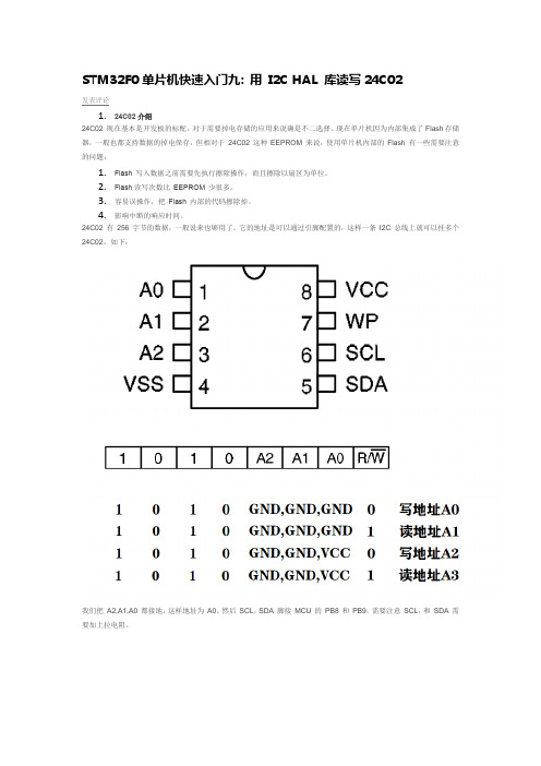
它的地址是可以通过引脚配置的,这样一条I2C 总线上就可以挂多个24C02。
如下:我们把A2,A1,A0 都接地,这样地址为A0。
然后SCL,SDA 脚接MCU 的PB8 和PB9。
需要注意SCL,和SDA 需要加上拉电阻。
1.代码下面我们在一个I2C 例程上面修改代码来实现24C02 的读写。
大家可以看到使用库函数的好处,基本上不用看STM32F030 的手册,很快就能实现我们想要实现的功能。
我们用Keil 打开下面这个工程:STM32Cube_FW_F0_V1.11.0\Projects\STM32F030R8-Nucleo\Examples\I2C\I2C_TwoBoards_ComPolling\MDK-AR M\Project.uvprojxStep 1, 把I2C 地址改为跟我们硬件一致:Step 2, 根据实际使用的I2C 模块和引脚进行配置:Step 3, 把地址模式改为7BIT:Step 4, 操作EEPROM,我们不使用例子中的HAL_I2C_Master_Transmit 和HAL_I2C_Master_Receive,这两个函数适用于两个I2C 器件之间进行数据传输。
我们这里要用的是下面这两个函数:HAL_I2C_Mem_Write(I2C_HandleTypeDef *hi2c, // 使用的I2C 模块的Handle 的指针uint16_t DevAddress, // I2C 器件的地址,这里是24C02 的地址0xA0uint16_t MemAddress, // 存储器内部地址uint16_t MemAddSize, // 存储器内部地址位数8BIT or 16BIT ?uint8_t *pData, // 发送数据缓冲区指针uint16_t Size, // 数据长度uint32_t Timeout // 超时设置);HAL_I2C_Mem_Read(I2C_HandleTypeDef *hi2c, // 使用的I2C 模块的Handle 的指针uint16_t DevAddress, // I2C 器件的地址,这里是24C02 的地址0xA0uint16_t MemAddress, // 存储器内部地址uint16_t MemAddSize, // 存储器内部地址位数8BIT or 16BIT ?uint8_t *pData, // 接收数据缓冲区指针uint16_t Size, // 接收数据长度uint32_t Timeout // 超时设置);在此我们写入数据用的24C02 的Page Write 命令,每次写入8个字节的数据,然后存储器写入地址加8。
I2C读写EEPROM问题总结
2017 年6 月3 0 日星期五目的:利用TMS320F2801芯片上外设I2C (2线串口)读写EEPROM数据(24LC128)关键点1 : 24LC时钟频率400KHZ,寄存器设置如下://Prescaler- need7-12Mhzo nm oduleclk=10; 〃NOTE:mustbe non zero=5; 〃NOTE:mustbe non zero时钟频率也可设为200KHz,三个参数分别为9、20、20(CPU时钟频率为100MHz)(未测试)关键点2 :波形分析问题:I2C模块是不是只有I2CCNT减到0才会发出停止信号I2C模块是硬件的,当检测到发送完了就会发结束自动发信号,不需要人为干预问题1:字节写操作正常,但是字节读函数出错原因:写EEPROM是在七位器件地址后添加写标志,而读EEPROM需要在七位器件地址后添加写标志。
关键点:读EEPROM数据需要发送两次命令。
第一次为写地址(此地址会被赋值给EEPROM 内的地址指针),因此需要添加写标志;第二次为读数据,将写标志改为读标志。
问题2:主机接收时,SDA数据线上有数据传输,且I2CDRR接收数据寄存器有数据更新,但寄存器显示不可读,即CPU认为一直没接收到数据,一直停在下面语句while!=1);关键点:初始化设置时采用的是FIF O接收方式,因此无效,应查询FIF O接收中断位while!=1);//FIFORX 方式查询位。
此位只有在非FIFO中断接收方式时才有效。
问题3:断续单字节读写正常,但是采用连续的单字节读写出错。
原因:EEPRO M写过程的结束并不是I2C总线写结束就结束,实际上I2C总线的写入数据先被保存到了EEPRO M内部的缓冲区,当遇到I2C结束条件后,EEPROM才启动内部写过程,这个过程才是保存数据的过程。
非常悲哀的是这个过程比较长,官方文档标注为5ms。
如果在这5ms以内对EEPROM芯片访问将被忽略。
STM32系统学习——I2C (读写EEPROM)
STM32 系统学习——I2C (读写EEPROM)
I2C 通讯协议(Inter-Integrated Circuit)引脚少,硬件实现简单,可扩展性强,不需要USART、CAN 等通讯协议的外部收发设备,现在被广泛地使用在系统内多个集成电路(IC)间的通讯。
在计算机科学里,大部分复杂的问题都可以通过分层来简化。
如芯片被分为
内核层和片上外设;STM32 标准库则是在寄存器与用户代码之间的软件层。
对于通讯协议,我们也以分层的方式来理解,最基本的是把它分为物理层和协
议层。
物理层规定通讯系统中具有机械、电子功能部分的特性,确保原始数据在物
理媒体的传输。
协议层主要规定通讯逻辑,统一收发双方的数据打包、解包标准。
简单来说物理层规定我们用嘴巴还是用肢体来交流,
协议层则规定我们用中文还是英文来交流。
一、I2C 物理层
它的物理层有如下特点:
(1) 它是一个支持设备的总线。
“总线”指多个设备共用的信号线。
在一个I2C 通讯总线中,可连接多个I2C 通讯设备,支持多个通讯主机及多个通讯从机。
(2) 一个I2C 总线只使用两条总线线路,一条双向串行数据线(SDA) ,一条串行时钟线(SCL)。
数据线即用来表示数据,时钟线用于数据收发同步。
(3) 每个连接到总线的设备都有一个独立的地址,主机可以利用这个地址进行不同设备之间的访问。
(4) 总线通过上拉电阻接到电源。
当I2C 设备空闲时,会输出高阻态,而当所有设备都空闲,都输出高阻态时,由上拉电阻把总线拉成高电平。
STM32 模拟IIC读写24C02程序代码

STM32 模拟IIC读写24C02程序代码最近用到STM32F103V来读写A T24C02 EEPROM 于是从原来51单片机的程序代码的基础上修改了下,移植到了STM32,测试工作正常。
引脚定义和配置:#define SCL GPIO_Pin_6 //24C02 SCL#define SDA GPIO_Pin_7 //24C02 SDAvoid GPIO_Configuration(void){RCC_APB2PeriphClockCmd( RCC_APB2Periph_USART1 |RCC_APB2Periph_GPIOA | RCC_APB2Periph_GPIOB |RCC_APB2Periph_GPIOC | RCC_APB2Periph_GPIOD |RCC_APB2Periph_GPIOE, ENABLE);GPIO_InitStructure.GPIO_Pin = SCL; //24C02 SC LGPIO_InitStructure.GPIO_Mode = GPIO_Mode_Out_OD;GPIO_InitStructure.GPIO_Speed = GPIO_Speed_50MHz;GPIO_Init(GPIOB, &GPIO_InitStructure);GPIO_InitStructure.GPIO_Pin = SDA; //24C02 SDA 作为输出GPIO_InitStructure.GPIO_Mode = GPIO_Mode_Out_OD;GPIO_InitStructure.GPIO_Speed = GPIO_Speed_50MHz;GPIO_Init(GPIOB, &GPIO_InitStructure);}void AT24C02_SDA_IO_SET(unsigned char io_set) //SDA引脚输入输出设置{if(io_set==0){GPIO_InitStructure.GPIO_Pin = SDA; //24C02 SDA 作为输出GPIO_InitStructure.GPIO_Mode = GPIO_Mode_Out_OD;GPIO_InitStructure.GPIO_Speed = GPIO_Speed_50MHz;GPIO_Init(GPIOB, &GPIO_InitStructure);else if(io_set==1){GPIO_InitStructure.GPIO_Pin = SDA; //24C02 SDA 作为输入GPIO_InitStructure.GPIO_Mode = GPIO_Mode_IPU; //上拉输入GPIO_Init(GPIOB, &GPIO_InitStructure);}else{;}}////////////////////////////////////主程序////////////////////////////////////////////////////////////////////// ////////int main(void){ uchar i;uchar data_24c02;RCC_Configuration(); //时钟配置GPIO_Configuration();//GPIO配置USARTx_configuration();//串口配置WIN24C02_init();delayms(5000);//延时for(i=0;i<20;i++) //写EEPROM数据{ WIN24C02_write(0x00+i,i);delayms(100);}//存数据到EEPROMdelayms(1000);//延时while(1)//串口3发送读取的EEPROM的数据{for(i=0;i<20;i++){ data_24c02=WIN24C02_read(0x00+i);//读取24C02数据USART_SendData(USART3 ,data_24c02);while(USART_GetFlagStatus(USART3,USART_FLAG_TC)==RESET);}delayms(5000);//延时}/////////////////////////////////////////////////////////////////////////////////////////////////////////////////WIN_24C02.H头文件/**********************中文版本*******************************//*****功能描述: STM32 24C02 读写程序*****//*****作者: 郑文(ClimberWin) *****//*****编写日期: 2013年1月21日*****//*****版本信息: V1.0 *****//*****修改日期: *****//*************************************************************/#ifndef __WIN24C02_H__#define __WIN24C02_H__#include"STM32_Config.h"#define uchar unsigned char#define uint unsigned intuchar WIN24C02_read(uchar address); //从24c02的地址address中读取一个字节数据void WIN24C02_write(uchar address,uchar info); //向24c02的address地址中写入一字节数据infovoid WIN24C02_init(); //24c02初始化子程序void delay_nop(void);void delay2(uint x);void start();void stop();void writex(uchar j);uchar readx();void clock();void delay2(uint x){uint i;for(i=0;i<x;i++);}void delay_nop(void){uint8_t i=10; //i=10延时1.5us//这里可以优化速度,经测试最低到5还能写入while(i--);}void WIN24C02_init(){//SCL=1;GPIO_SetBits(GPIOB,SCL);delay_nop();//SDA=1;GPIO_SetBits(GPIOB,SDA);delay_nop();}void start(){//SDA=1;GPIO_SetBits(GPIOB,SDA);delay_nop();//SCL=1;GPIO_SetBits(GPIOB,SCL);delay_nop();//SDA=0;GPIO_ResetBits(GPIOB, SDA);delay_nop();//SCL=0;GPIO_ResetBits(GPIOB, SCL);delay_nop();}void stop(){//SDA=0;GPIO_ResetBits(GPIOB, SDA);delay_nop();//SCL=1;GPIO_SetBits(GPIOB,SCL);delay_nop();//SDA=1;GPIO_SetBits(GPIOB,SDA);delay_nop();}void writex(uchar j){uchar i,temp,temp1;temp=j;//A T24C02_SDA_IO_SET(0);for (i=0;i<8;i++){temp1=temp & 0x80;temp=temp<<1;//SCL=0;GPIO_ResetBits(GPIOB, SCL);delay_nop();//SDA=CY;if(temp1==0x80){GPIO_SetBits(GPIOB, SDA);} else{GPIO_ResetBits(GPIOB, SDA);} delay_nop();// SCL=1;GPIO_SetBits(GPIOB,SCL);delay_nop();}//A T24C02_SDA_IO_SET(0);//SCL=0;GPIO_ResetBits(GPIOB, SCL);delay_nop();//SDA=1;GPIO_SetBits(GPIOB,SDA);delay_nop();}uchar readx(){uchar i,j,k=0;//SCL=0;GPIO_ResetBits(GPIOB, SCL);delay_nop();//SDA=1;GPIO_SetBits(GPIOB,SDA);AT24C02_SDA_IO_SET(1);for (i=0;i<8;i++){delay_nop();//SCL=1;GPIO_SetBits(GPIOB,SCL);delay_nop();//if (SDA==1) j=1;if( GPIO_ReadInputDataBit(GPIOB,SDA)==1 ) {j=1;}else{j=0;}k=(k<<1)|j;//SCL=0;GPIO_ResetBits(GPIOB, SCL);}AT24C02_SDA_IO_SET(0);delay_nop();return(k);}{uint i=0;AT24C02_SDA_IO_SET(1);//SCL=1;GPIO_SetBits(GPIOB,SCL);delay_nop();while ((GPIO_ReadInputDataBit(GPIOB,SDA)==1)&&(i<5000))i++;//SCL=0;GPIO_ResetBits(GPIOB, SCL);delay_nop();AT24C02_SDA_IO_SET(0);}uchar WIN24C02_read(uchar address){uchar i;start();writex(0xa0);clock();writex(address);clock();start();writex(0xa1);clock();i=readx();stop();//delay2(10);delay2(50);return(i);}void WIN24C02_write(uchar address,uchar info){start();writex(0xa0);clock();writex(address);writex(info);clock();stop();//delay2(50);delay2(250); }#endif。
CAT24C128 EEPROM 128Kb I2C 说明书
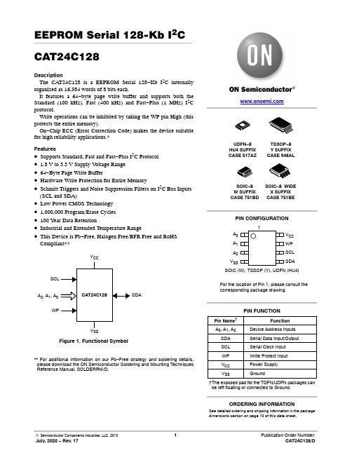
EEPROM Serial 128-Kb I2C CAT24C128DescriptionThe CAT24C128 is a EEPROM Serial 128−Kb I2C internally organized as 16,384 words of 8 bits each.It features a 64−byte page write buffer and supports both the Standard (100 kHz), Fast (400 kHz) and Fast−Plus (1 MHz) I2C protocol.Write operations can be inhibited by taking the WP pin High (this protects the entire memory).On−Chip ECC (Error Correction Code) makes the device suitable for high reliability applications.*Features•Supports Standard, Fast and Fast−Plus I2C Protocol•1.8 V to 5.5 V Supply V oltage Range•64−Byte Page Write Buffer•Hardware Write Protection for Entire Memory•Schmitt Triggers and Noise Suppression Filters on I2C Bus Inputs (SCL and SDA)•Low Power CMOS Technology•1,000,000 Program/Erase Cycles•100 Year Data Retention•Industrial and Extended Temperature Range•This Device is Pb−Free, Halogen Free/BFR Free and RoHS Compliant**Figure 1. Functional Symbol SDASCLWPV CCSSA2, A1, A0** For additional information on our Pb−Free strategy and soldering details,please download the ON Semiconductor Soldering and Mounting Techniques Reference Manual, SOLDERRM/D.PIN CONFIGURATIONSDAWPV CCV SSA2A1A01See detailed ordering and shipping information in the package dimensions section on page 10 of this data sheet.ORDERING INFORMATIONSOIC−8W SUFFIXCASE 751BDSCLSOIC (W), TSSOP (Y), UDFN (HU4)TSSOP−8Y SUFFIXCASE 948ALDevice Address Inputs A0, A1, A2Serial Data Input/OutputSDASerial Clock InputSCLWrite Protect InputWPPower SupplyV CCGroundV SSFunctionPin Name†PIN FUNCTIONFor the location of Pin 1, please consult thecorresponding package drawing.UDFN−8HU4 SUFFIXCASE 517AZ†The exposed pad for the TDFN/UDFN packages canbe left floating or connected to Ground.SOIC−8 WIDEX SUFFIXCASE 751BETable 1. ABSOLUTE MAXIMUM RATINGSParameter Rating Units Storage Temperature−65 to +150°C Voltage on Any Pin with Respect to Ground (Note 1)−0.5 to +6.5V Stresses exceeding those listed in the Maximum Ratings table may damage the device. If any of these limits are exceeded, device functionality should not be assumed, damage may occur and reliability may be affected.1.The DC input voltage on any pin should not be lower than −0.5 V or higher than V CC + 0.5 V. During transitions, the voltage on any pin mayundershoot to no less than −1.5 V or overshoot to no more than V CC + 1.5 V, for periods of less than 20 ns.Table 2. RELIABILITY CHARACTERISTICS (Note 2)Symbol Parameter Min UnitsN END (Notes 3, 4)Endurance1,000,000Program / Erase Cycles T DR Data Retention100Years2.These parameters are tested initially and after a design or process change that affects the parameter according to appropriate AEC−Q100and JEDEC test methods.3.Page Mode, V CC = 5 V, 25°C4.The new product revision (C) uses ECC (Error Correction Code) logic with 6 ECC bits to correct one bit error in 4 data bytes. Therefore, whena single byte has to be written, 4 bytes (including the ECC bits) are re−programmed. It is recommended to write by multiple of 4 bytes in orderto benefit from the maximum number of write cycles.Table 3. D.C. OPERATING CHARACTERISTICS(V CC = 1.8 V to 5.5 V, T A = −40°C to +85°C and V CC = 2.5 V to 5.5 V, T A = −40°C to +125°C, unless otherwise specified.)Symbol Parameter Test Conditions Min Max UnitsI CCR Read Current Read, f SCL = 400 kHz/1 MHz1mAI CCW Write Current3mAI SB Standby Current All I/O Pins at GND or V CC T A = −40°C to +85°C2m AT A = −40°C to +125°C5I L I/O Pin Leakage Pin at GND or V CC T A = −40°C to +85°C1m AT A = −40°C to +125°C2 V IL1Input Low Voltage 2.5 V ≤ V CC≤ 5.5 V−0.50.3 V CC V V IL2Input Low Voltage 1.8 V ≤ V CC < 2.5 V−0.50.25 V CC V V IH1Input High Voltage 2.5 V ≤ V CC≤ 5.5 V0.7 V CC V CC + 0.5V V IH2Input High Voltage 1.8 V ≤ V CC < 2.5 V0.75 V CC V CC + 0.5V V OL1Output Low Voltage V CC≥ 2.5 V, I OL = 3.0 mA0.4V V OL2Output Low Voltage V CC < 2.5 V, I OL = 1.0 mA0.2V Table 4. PIN IMPEDANCE CHARACTERISTICS(V CC = 1.8 V to 5.5 V, T A = −40°C to +85°C and V CC = 2.5 V to 5.5 V, T A = −40°C to +125°C, unless otherwise specified.) Symbol Parameter Conditions Max UnitsC IN (Note 5)SDA I/O Pin Capacitance V IN = 0 V8pFC IN (Note 5)Input Capacitance (other pins)V IN = 0 V6pFI WP, I A (Note 6)WP Input Current, Address InputCurrent (A0, A1, A2)V IN< V IH, V CC = 5.5 V75m A V IN< V IH, V CC = 3.3 V50V IN< V IH, V CC = 1.8 V25V IN> V IH25.These parameters are tested initially and after a design or process change that affects the parameter according to appropriate AEC−Q100and JEDEC test methods.6.When not driven, the WP, A0, A1, A2 pins are pulled down to GND internally. For improved noise immunity, the internal pull−down is relativelystrong; therefore the external driver must be able to supply the pull−down current when attempting to drive the input HIGH. T o conserve power, as the input level exceeds the trip point of the CMOS input buffer (~ 0.5 x V CC), the strong pull−down reverts to a weak current source.Table 5. A.C. CHARACTERISTICS(V CC = 1.8 V to 5.5 V, T A = −40°C to +85°C and V CC = 2.5 V to 5.5 V, T A = −40°C to +125°C)(Note 7)Symbol ParameterStandardV CC = 1.8 V − 5.5 VFastV CC = 1.8 V − 5.5 VFast−Plus (Note 10)V CC = 2.5 V − 5.5 VT A = −405C to +855CUnits Min Max Min Max Min MaxF SCL Clock Frequency1004001,000kHzt HD:STA START Condition Hold Time40.60.25m s t LOW Low Period of SCL Clock 4.7 1.30.45m s t HIGH High Period of SCL Clock40.60.40m s t SU:STA START Condition Setup Time 4.70.60.25m s t HD:DAT Data In Hold Time000m s t SU:DAT Data In Setup Time25010050ns t R (Note 8)SDA and SCL Rise Time1,000300100ns t F (Note 8)SDA and SCL Fall Time300300100ns t SU:STO STOP Condition Setup Time40.60.25m s t BUF Bus Free Time BetweenSTOP and START4.7 1.30.5m st AA SCL Low to Data Out Valid 3.50.90.40m s t DH Data Out Hold Time10010050ns T i (Note 8)Noise Pulse Filtered at SCLand SDA Inputs10010050ns t SU:WP WP Setup Time000m s t HD:WP WP Hold Time 2.5 2.51m s t WR Write Cycle Time555mst PU(Notes 8, 9)Power-up to Ready Mode110.11ms7.Test conditions according to “A.C. Test Conditions” table.8.Tested initially and after a design or process change that affects this parameter.9.t PU is the delay between the time V CC is stable and the device is ready to accept commands.10.Fast−Plus (1 MHz) speed class available for new product revision “C”. The die revision “C” is identified by letter “C” or a dedicated markingcode on top of the package.Table 6. A.C. TEST CONDITIONSInput Levels0.2 x V CC to 0.8 x V CCInput Rise and Fall Times v 50 nsInput Reference Levels0.3 x V CC, 0.7 x V CCOutput Reference Levels0.5 x V CCOutput Load Current Source: I OL = 3 mA (V CC≥ 2.5 V); I OL = 1 mA (V CC < 2.5 V); C L = 100 pFPower−On Reset (POR)The CAT24C128 incorporates Power−On Reset (POR) circuitry which protects the device against powering up in the wrong state.The CAT24C128 will power up into Standby mode after V CC exceeds the POR trigger level and will power down into Reset mode when V CC drops below the POR trigger level. This bi−directional POR feature protects the device against ‘brown−out’ failure following a temporary loss of power. Pin DescriptionSCL: The Serial Clock input pin accepts the Serial Clock generated by the Master.SDA: The Serial Data I/O pin receives input data and transmits data stored in EEPROM. In transmit mode, this pin is open drain. Data is acquired on the positive edge, and is delivered on the negative edge of SCL.A0, A1 and A2: The Address pins accept the device address. When not driven, these pins are pulled LOW internally. WP: The Write Protect input pin inhibits all write operations, when pulled HIGH. When not driven, this pin is pulled LOW internally.Functional DescriptionThe CAT24C128 supports the Inter−Integrated Circuit (I2C) Bus data transmission protocol, which defines a device that sends data to the bus as a transmitter and a device receiving data as a receiver. Data flow is controlled by a Master device, which generates the serial clock and all START and STOP conditions. The CAT24C128 acts as a Slave device. Master and Slave alternate as either transmitter or receiver. Up to 8 devices may be connected to the bus as determined by the device address inputs A0, A1, and A2.I2C Bus ProtocolThe I2C bus consists of two ‘wires’, SCL and SDA. The two wires are connected to the V CC supply via pull−up resistors. Master and Slave devices connect to the 2−wire bus via their respective SCL and SDA pins. The transmitting device pulls down the SDA line to ‘transmit’ a ‘0’ and releases it to ‘transmit’ a ‘1’.Data transfer may be initiated only when the bus is not busy (see A.C. Characteristics).During data transfer, the SDA line must remain stable while the SCL line is HIGH. An SDA transition while SCL is HIGH will be interpreted as a START or STOP condition (Figure 2). The START condition precedes all commands. It consists of a HIGH to LOW transition on SDA while SCL is HIGH. The START acts as a ‘wake−up’ call to all receivers. Absent a START, a Slave will not respond to commands. The STOP condition completes all commands. It consists of a LOW to HIGH transition on SDA while SCL is HIGH.Device AddressingThe Master initiates data transfer by creating a START condition on the bus. The Master then broadcasts an 8−bit serial Slave address. The first 4 bits of the Slave address are set to 1010, for normal Read/Write operations (Figure 3). The next 3 bits, A2, A1 and A0, select one of 8 possible Slave devices and must match the state of the external address pins. The last bit, R/W, specifies whether a Read (1) or Write (0) operation is to be performed.AcknowledgeAfter processing the Slave address, the Slave responds with an acknowledge (ACK) by pulling down the SDA line during the 9th clock cycle (Figure 4). The Slave will also acknowledge all address bytes and every data byte presented in Write mode. In Read mode the Slave shifts out a data byte, and then releases the SDA line during the 9th clock cycle. As long as the Master acknowledges the data, the Slave will continue transmitting. The Master terminates the session by not acknowledging the last data byte (NoACK) and by issuing a STOP condition. Bus timing is illustrated in Figure 5.START CONDITIONSTOP CONDITIONSDASCLFigure 2. START/STOP ConditionsDEVICE ADDRESSFigure 3. Slave Address BitsSCL FROM MASTER≥ t SU:DAT )DATA OUTPUTFROM TRANSMITTERDATA OUTPUT FROM RECEIVERFigure 4. Acknowledge TimingSCLSDA INSDA OUTFigure 5. Bus TimingWrite OperationsByte WriteUpon receiving a Slave address with the R/W bit set to ‘0’,the CA T24C128 will interpret the next two bytes as address bytes. These bytes are used to initialize the internal address counter; the 2 most significant bits are ‘don’t care’, the next 8 point to one of 256 available pages and the last 6 point to a location within a 64 byte page. A byte following the address bytes will be interpreted as data. The data will be loaded into the Page Write Buffer and will eventually be written to memory at the address specified by the 14 active address bits provided earlier. The CAT24C128 will acknowledge the Slave address, address bytes and data byte.The Master then starts the internal Write cycle by issuing a STOP condition (Figure 6). During the internal Write cycle (t WR ), the SDA output will be tri −stated and additional Read or Write requests will be ignored (Figure 7).Page WriteBy continuing to load data into the Page Write Buffer after the 1st data byte and before issuing the STOP condition, up to 64 bytes can be written simultaneously during one internal Write cycle (Figure 8). If more data bytes are loaded than locations available to the end of page, then loading will continue from the beginning of page, i.e. the page address islatched and the address count automatically increments to and then wraps −around at the page boundary. Previously loaded data can thus be overwritten by new data. What is eventually written to memory reflects the latest Page Write Buffer contents. Only data loaded within the most recent Page Write sequence will be written to memory.Acknowledge PollingThe ready/busy status of the CAT24C128 can be ascertained by sending Read or Write requests immediately following the STOP condition that initiated the internal Write cycle. As long as internal Write is in progress, the CAT24C128 will not acknowledge the Slave address.Hardware Write ProtectionWith the WP pin held HIGH, the entire memory is protected against Write operations. If the WP pin is left floating or is grounded, it has no impact on the operation of the CAT24C128. The state of the WP pin is strobed on the last falling edge of SCL immediately preceding the first data byte (Figure 9). If the WP pin is HIGH during the strobe interval, the CA T24C128 will not acknowledge the data byte and the Write request will be rejected.Delivery StateThe CAT24C128 is shipped erased, i.e., all bytes are FFh.SLAVE ADDRESSSA C KA C KA C KS T O P PBUS ACTIVITY:MASTERSLAVES T AR T ADDRESS BYTE ADDRESS BYTE DATA BYTEA C K* = Don’t Care BitFigure 6. Byte Write Sequence**a 13−a 8a 7−a 0STOPCONDITIONSTARTCONDITIONADDRESSSCLSDA Figure 7. Write Cycle TimingSLAVE ADDRESSSA C KA C KC KBUS ACTIVITY:MASTER SLAVEST ARTADDRESS BYTE ADDRESS BYTE DATA BYTE DATA BYTE DATABYTE C KS T O C KC KC K* = Don’t Care Bit P v 63Figure 8. Page Write Sequence**a 13−a 8a 7−a 0ADDRESS BYTEDATA BYTESCLSDA WPFigure 9. WP TimingRead OperationsImmediate ReadUpon receiving a Slave address with the R/W bit set to ‘1’,the CAT24C128 will interpret this as a request for data residing at the current byte address in memory. The CAT24C128 will acknowledge the Slave address, will immediately shift out the data residing at the current address,and will then wait for the Master to respond. If the Master does not acknowledge the data (NoACK) and then follows up with a STOP condition (Figure 10), the CAT24C128returns to Standby mode.Selective ReadTo read data residing at a specific location, the internal address counter must first be initialized as described under Byte Write. If rather than following up the two address byteswith data, the Master instead follows up with an Immediate Read sequence, then the CAT24C128 will use the 14 active address bits to initialize the internal address counter and will shift out data residing at the corresponding location. If the Master does not acknowledge the data (NoACK) and then follows up with a STOP condition (Figure 11), the CAT24C128 returns to Standby mode.Sequential ReadIf during a Read session the Master acknowledges the 1st data byte, then the CAT24C128 will continue transmitting data residing at subsequent locations until the Master responds with a NoACK, followed by a STOP (Figure 12).In contrast to Page Write, during Sequential Read the address count will automatically increment to and then wrap −around at end of memory (rather than end of page).SCL SDA 8th Bit STOPNO ACKDATA OUT8SLAVE ADDRESSSA C KDATA BYTEN O A C K S T O P PS T A R T BUS ACTIVITY:MASTERSLAVEFigure 10. Immediate Read Sequence and Timing9SLAVE ADDRESSSA C KA C K A C K BUS ACTIVITY:MASTERSLAVES T A R T ADDRESS BYTE ADDRESS BYTE DATA BYTESLAVE ADDRESSSA C KP* = Don’t Care BitFigure 11. Selective Read Sequence**S T A R T S T O P A C KN O a 13−a 8a 7−a 0BUS ACTIVITY:MASTERSLAVEBYTE nBYTE n+1BYTE n+2BYTE n+xC KC KC KS T O N O A C C KSLAVE Figure 12. Sequential Read SequenceORDERING INFORMATION(Notes 11 thru 14)Device Order Number SpecificDeviceMarking*PackageType Temperature Range Lead Finish Shipping†CAT24C128WI−GT324128C SOIC−8,JEDECI = Industrial(−40°C to +85°C)NiPdAu Tape & Reel,3,000 Units / ReelCAT24C128YI−GT3C28C TSSOP−8I = Industrial(−40°C to +85°C)NiPdAu Tape & Reel,3,000 Units / ReelCAT24C128HU4IGT3C7U UDFN−8I = Industrial(−40°C to +85°C)NiPdAu Tape & Reel,3,000 Units / Reel†For information on tape and reel specifications, including part orientation and tape sizes, please refer to our Tape and Reel Packaging Specifications Brochure, BRD8011/D.11.All packages are RoHS−compliant (Lead−free, Halogen−free).12.The standard lead finish is NiPdAu.13.For additional package and temperature options, please contact your nearest ON Semiconductor Sales office.14.For detailed information and a breakdown of device nomenclature and numbering systems, please see the ON Semiconductor DeviceNomenclature document, TND310/D, available at ON Semiconductor is licensed by the Philips Corporation to carry the I2C bus protocol.UDFN8, 2x3 EXTENDED PADCASE 517AZ ISSUE ADATE 23 MAR 2015SCALE 2:1NOTES:1.DIMENSIONING AND TOLERANCING PER ASME Y14.5M, 1994.2.CONTROLLING DIMENSION: MILLIMETERS.3.DIMENSION b APPLIES TO PLATEDTERMINAL AND IS MEASURED BETWEEN 0.15 AND 0.25MM FROM THE TERMINAL TIP .4.COPLANARITY APPLIES TO THE EXPOSEDPAD AS WELL AS THE TERMINALS.DIM MIN MAX MILLIMETERS A 0.450.55A10.000.05b 0.200.30D 2.00 BSC D2 1.35 1.45E 3.00 BSC E2 1.25 1.35e 0.50 BSC L 0.250.35*For additional information on our Pb −Free strategy and soldering details, please download the ON Semiconductor Soldering and Mounting Techniques Reference Manual, SOLDERRM/D.SOLDERING FOOTPRINT*DIMENSIONS: MILLIMETERSDETAIL AA30.13 REF L1DETAIL ALALTERNATE CONSTRUCTIONSLL1−−−0.15RECOMMENDEDGENERICMARKING DIAGRAM*XXXXX = Specific Device Code A = Assembly Location WL = Wafer Lot Y = YearW = Work WeekG= Pb −Free Package*This information is generic. Please refer to device data sheet for actual part marking.Pb −Free indicator, “G” or microdot “ G ”,may or may not be present.XXXXX AWLYW G18XDETAIL BALTERNATE CONSTRUCTIONSSOIC −8, 150 mils CASE 751BD ISSUE ODATE 19 DEC 2008IDENTIFICATIONTOP VIEWSIDE VIEWEND VIEWNotes:(1) All dimensions are in millimeters. Angles in degrees.(2) Complies with JEDEC MS-012.SYMBOLMIN NOM MAX θA A1b cD E E1e h 0º8º0.100.330.190.254.805.803.801.27 BSC1.750.250.510.250.505.006.204.00L0.401.271.35TSSOP8, 4.4x3.0, 0.65PCASE 948AL ISSUE ADATE 20 MAY 2022qXXX = Specific Device Code Y = YearWW = Work WeekA = Assembly Location G= Pb −Free Package*This information is generic. Please refer to device data sheet for actual part marking.Pb −Free indicator, “G” or microdot “G ”, may or may not be present. Some products may not follow the Generic Marking.GENERICMARKING DIAGRAM*XXX YWW A GPUBLICATION ORDERING INFORMATIONTECHNICAL SUPPORTLITERATURE FULFILLMENT:。
常用EEPROM资料-24C128
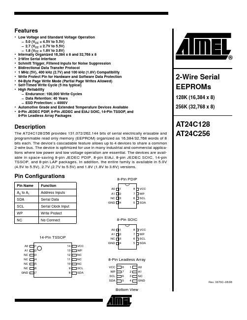
Features•Low Voltage and Standard Voltage Operation–5.0 (V CC = 4.5V to 5.5V)–2.7 (V CC = 2.7V to 5.5V)–1.8 (V CC = 1.8V to 3.6V)•Internally Organized 16,384 x 8 and 32,768 x 8•2-Wire Serial Interface•Schmitt Trigger, Filtered Inputs for Noise Suppression •Bidirectional Data Transfer Protocol• 1 MHz (5V), 400 kHz (2.7V) and 100 kHz (1.8V) Compatibility •Write Protect Pin for Hardware and Software Data Protection •64-Byte Page Write Mode (Partial Page Writes Allowed)•Self-Timed Write Cycle (5 ms typical)•High Reliability–Endurance: 100,000 Write Cycles –Data Retention: 40 Years –ESD Protection: > 4000V•Automotive Grade and Extended Temperature Devices Available •8-Pin JEDEC PDIP , 8-Pin JEDEC and EIAJ SOIC, 14-Pin TSSOP , and 8-Pin Leadless Array PackagesDescriptionThe AT24C128/256 provides 131,072/262,144 bits of serial electrically erasable and programmable read only memory (EEPROM) organized as 16,384/32,768 words of 8bits each. The device’s cascadable feature allows up to 4 devices to share a common 2-wire bus. The device is optimized for use in many industrial and commercial applica-tions where low power and low voltage operation are essential. The devices are avail-able in space-saving 8-pin JEDEC PDIP, 8-pin EIAJ, 8-pin JEDEC SOIC, 14-pin TSSOP, and 8-pin LAP packages. In addition, the entire family is available in 5.0V (4.5V to 5.5V), 2.7V (2.7V to 5.5V) and 1.8V (1.8V to 3.6V) versions.Pin ConfigurationsPin Name Function A 0 to A 1Address Inputs SDA Serial Data SCL Serial Clock Input WP Write Protect NCNo Connect8-Pin PDIP8-Pin SOIC8-Pin Leadless ArrayBottom View14-Pin TSSOPAbsolute Maximum Ratings*Block DiagramPin DescriptionSERIAL CLOCK (SCL): The SCL input is used to positive edge clock data into each EEPROM device and negative edge clock data out of each device.SERIAL DATA (SDA): The SDA pin is bidirectional for serial data transfer. This pin is open-drain driven and may be wire-ORed with any number of other open-drain or open collector devices.DEVICE/PAGE ADDRESSES (A1, A0): The A1 and A0pins are device address inputs that are hardwired or left not connected for hardware compatibility with AT24C32/64.When the pins are hardwired, as many as four 128K/256K devices may be addressed on a single bus system (device addressing is discussed in detail under the Device Addressing section). When the pins are not hardwired, the default A 1 and A 0 are zero.WRITE PROTECT (WP): The write protect input, when tied to GND, allows normal write operations. When WP is tied high to V CC , all write operations to the memory are inhib-ited. If left unconnected, WP is internally pulled down to GND. Switching WP to V CC prior to a write operation cre-ates a software write protect function.Memory OrganizationAT24C128/256, 128K/256K SERIAL EEPROM: The 128K/256K is internally organized as 256/512 pages of 64-bytes each. Random word addressing requires a 14/15-bit data word address.Operating T emperature..................................-55°C to +125°C *NOTICE:Stresses beyond those listed under “Absolute Maximum Ratings” may cause permanent dam-age to the device. This is a stress rating only and functional operation of the device at these or any other conditions beyond those indicated in the operational sections of this specification is not implied. Exposure to absolute maximum rating conditions for extended periods may affect device reliability .Storage T emperature.....................................-65°C to +150°C Voltage on Any Pinwith Respect to Ground.....................................-1.0V to +7.0V Maximum Operating Voltage...........................................6.25V DC Output Current........................................................5.0 mAAT24C128/256Pin Capacitance (1)Applicable over recommended operating range from T A = 25°C, f = 1.0 MHz, V CC = +1.8V.Note:This parameter is characterized and is not 100% tested.DC CharacteristicsApplicable over recommended operating range from: T AI = -40°C to +85°C, V CC = +1.8V to +5.5V, T AC = 0°C to +70°C,V CC = +1.8V to +5.5V (unless otherwise noted).Note:V IL min and V IH max are reference only and are not testedSymbol Test ConditionMax Units Conditions C I/O Input/Output Capacitance (SDA)8pF V I/O = 0V C IN Input Capacitance (A 0, A 1, SCL)6pFV IN = 0VSymbol Parameter Test ConditionMin TypMax Units V CC1Supply Voltage 1.8 3.6V V CC2Supply Voltage 2.7 5.5V V CC3Supply Voltage 4.55.5V I CC1Supply Current V CC = 5.0V READ at 400 kHz 1.0 2.0mA I CC2Supply Current V CC = 5.0V WRITE at 400 kHz 2.0 3.0mA I SB1Standby Current (1.8V option)V CC = 1.8V V IN = V CC or V SS0.2µAV CC = 3.6V 2.0I SB2Standby Current (2.7V option)V CC = 2.7V V IN = V CC or V SS 0.5µA V CC = 5.5V 6.0I SB3Standby Current (5.0V option)V CC = 4.5 - 5.5VV IN = V CC or V SS 6.0µA I LI Input Leakage Current V IN = V CC or V SS 0.10 3.0µA I LO Output Leakage Current V OUT = V CC or V SS0.053.0µA V IL Input Low Level (Note:)-0.6V CC x 0.3V V IH Input High Level (Note:)V CC x 0.7V CC + 0.5V V OL2Output Low Level V CC = 3.0V I OL = 2.1 mA 0.4V V OL1Output Low LevelV CC = 1.8VI OL = 0.15 mA0.2VAC CharacteristicsApplicable over recommended operating range from T A = -40°C to +85°C, V CC = +1.8V to +5.5V, CL = 100 pF (unless oth-erwise noted). Test conditions are listed in Note 2.Notes: 1.This parameter is characterized and is not 100% tested.2.AC measurement conditions:R L (connects to V CC): 1.3KΩ (2.7V, 5V), 10KΩ (1.8V)Input pulse voltages: 0.3V CC to 0.7V CCInput rise and fall times: ≤50nsInput and output timing reference voltages: 0.5V CCDevice OperationCLOCK and DATA TRANSITIONS: The SDA pin is nor-mally pulled high with an external device. Data on the SDA pin may change only during SCL low time periods (refer to Data Validity timing diagram). Data changes during SCL high periods will indicate a start or stop condition as defined below.START CONDITION: A high-to-low transition of SDA with SCL high is a start condition which must precede any other command (refer to Start and Stop Definition timing dia-gram).STOP CONDITION: A low-to-high transition of SDA with SCL high is a stop condition. After a read sequence, the stop command will place the EEPROM in a standby power mode (refer to Start and Stop Definition timing diagram).ACKNOWLEDGE: All addresses and data words are seri-ally transmitted to and from the EEPROM in 8-bit words. The EEPROM sends a zero during the ninth clock cycle to acknowledge that it has received each word.STANDBY MODE: The AT24C128/256 features a low power standby mode which is enabled: a) upon power-up and b) after the receipt of the STOP bit and the completion of any internal operations.MEMORY RESET: After an interruption in protocol, power loss or system reset, any 2-wire part can be reset by follow-ing these steps: (a) Clock up to 9 cycles, (b) look for SDA high in each cycle while SCL is high and then (c) create a start condition as SDA is high.Symbol Parameter1.8-volt2.7-volt 5.0-voltUnits Min Max Min Max Min Maxf SCL Clock Frequency, SCL1004001000kHz t LOW Clock Pulse Width Low 4.7 1.30.6µs t HIGH Clock Pulse Width High 4.0 1.00.4µs t AA Clock Low to Data Out Valid0.1 4.50.050.90.050.55µst BUF Time the bus must be free before a newtransmission can start(1)4.7 1.30.5µst HD.ST A Start Hold Time 4.00.60.25µs t SU.ST A Start Set-up Time 4.70.60.25µs t HD.DA T Data In Hold Time000µs t SU.DA T Data In Set-up Time200100100ns t R Inputs Rise Time(1) 1.00.30.3µs t F Inputs Fall Time(1)300300100ns t SU.STO Stop Set-up Time 4.70.60.25µs t DH Data Out Hold Time1005050ns t WR Write Cycle Time201010msEndurance(1) 5.0V, 25°C, Page Mode100K100K100KWrite CyclesAT24C128/256 Bus Timing (SCL: Serial Clock, SDA: Serial Data I/O)Write Cycle Timing (SCL: Serial Clock, SDA: Serial Data I/O)Note: 1.The write cycle time t WR is the time from a valid stop condition of a write sequence to the end of the internal clear/write cycle.Data ValidityStart and Stop DefinitionOutput AcknowledgeAT24C128/256Device AddressingThe 128K/256K EEPROM requires an 8-bit device address word following a start condition to enable the chip for a read or write operation (refer to Figure 1). The device address word consists of a mandatory one, zero sequence for the first five most significant bits as shown. This is common to all 2-wire EEPROM devices.The 128K/256K uses the two device address bits A1, A0 to allow as many as four devices on the same bus. These bits must compare to their corresponding hardwired input pins. The A1 and A0 pins use an internal proprietary circuit that biases them to a logic low condition if the pins are allowed to float.The eighth bit of the device address is the read/write opera-tion select bit. A read operation is initiated if this bit is high and a write operation is initiated if this bit is low.Upon a compare of the device address, the EEPROM will output a zero. If a compare is not made, the device will return to a standby state.DATA SECURITY: The AT24C128/256 has a hardware data protection scheme that allows the user to write protect the whole memory when the WP pin is at V CC.Write OperationsBYTE WRITE: A write operation requires two 8-bit data word addresses following the device address word and acknowledgment. Upon receipt of this address, the EEPROM will again respond with a zero and then clock in the first 8-bit data word. Following receipt of the 8-bit data word, the EEPROM will output a zero. The addressing device, such as a microcontroller, then must terminate the write sequence with a stop condition. At this time the EEPROM enters an internally-timed write cycle, t WR, to the nonvolatile memory. All inputs are disabled during this write cycle and the EEPROM will not respond until the write is complete (refer to Figure 2).P AGE WRITE: The 128K/256K EEPROM is capable of 64-byte page writes.A page write is initiated the same way as a byte write, but the microcontroller does not send a stop condition after the first data word is clocked in. Instead, after the EEPROM acknowledges receipt of the first data word, the microcon-troller can transmit up to 63 more data words. The EEPROM will respond with a zero after each data word received. The microcontroller must terminate the page write sequence with a stop condition (refer to Figure 3). The data word address lower 6 bits are internally incre-mented following the receipt of each data word. The higher data word address bits are not incremented, retaining the memory page row location. When the word address, inter-nally generated, reaches the page boundary, the following byte is placed at the beginning of the same page. If more than 64 data words are transmitted to the EEPROM, the data word address will “roll over” and previous data will be overwritten. The address “roll over” during write is from the last byte of the current page to the first byte of the same page.ACKNOWLEDGE POLLING: Once the internally-timed write cycle has started and the EEPROM inputs are dis-abled, acknowledge polling can be initiated. This involves sending a start condition followed by the device address word. The read/write bit is representative of the operation desired. Only if the internal write cycle has completed will the EEPROM respond with a zero, allowing the read or write sequence to continue.Read OperationsRead operations are initiated the same way as write opera-tions with the exception that the read/write select bit in the device address word is set to one. There are three read operations: current address read, random address read and sequential read.CURRENT ADDRESS READ: The internal data word address counter maintains the last address accessed dur-ing the last read or write operation, incremented by one. This address stays valid between operations as long as the chip power is maintained. The address “roll over” during read is from the last byte of the last memory page, to the first byte of the first page.Once the device address with the read/write select bit set to one is clocked in and acknowledged by the EEPROM, the current address data word is serially clocked out. The microcontroller does not respond with an input zero but does generate a following stop condition (refer to Figure 4). RANDOM READ: A random read requires a “dummy” byte write sequence to load in the data word address. Once the device address word and data word address are clocked in and acknowledged by the EEPROM, the microcontroller must generate another start condition. The microcontroller now initiates a current address read by sending a device address with the read/write select bit high. The EEPROM acknowledges the device address and serially clocks out the data word. The microcontroller does not respond with a zero but does generate a following stop condition (refer to Figure 5).SEQUENTIAL READ: Sequential reads are initiated by either a current address read or a random address read. After the microcontroller receives a data word, it responds with an acknowledge. As long as the EEPROM receives an acknowledge, it will continue to increment the data word address and serially clock out sequential data words. When the memory address limit is reached, the data word address will “roll over” and the sequential read will con-tinue. The sequential read operation is terminated when the microcontroller does not respond with a zero but does generate a following stop condition (refer to Figure 6).Figure 1. Device AddressFigure 2. Byte WriteFigure 3. Page Write(* = DON’T CARE bit)(† = DON’T CARE bit for the 128K) Figure 4. Current Address ReadAT24C128/256 Figure 5. Random Read(* = DON’T CARE bit)(† = DON’T CARE bit for the 128K)Figure 6. Sequential ReadAT24C128 Ordering Informationt WR (max)(ms)I CC (max)(µA)I SB (max)(µA)f MAX(kHz)Ordering Code Package Operation Range103000 6.01000A T24C128-10PCA T24C128N-10SCA T24C128W-10SCA T24C128-10CCA T24C128C1-10CCA T24C128T1-10TC 8P38S18S28C8C114TCommercial(0°C to 70°C)3000 6.01000A T24C128-10PIA T24C128N-10SIA T24C128W-10SIA T24C128-10CIA T24C128C1-10CIA T24C128T1-10TI 8P38S18S28C8C114TIndustrial(-40°C to 85°C)1015000.5400A T24C128-10PC-2.7A T24C128N-10SC-2.7A T24C128W-10SC-2.7A T24C128-10CC-2.7A T24C128C1-10CC-2.7A T24C128T1-10TC-2.78P38S18S28C8C114TCommercial(0°C to 70°C)15000.5400A T24C128-10PI-2.7A T24C128N-10SI-2.7A T24C128W-10SI-2.7A T24C128-10CI-2.7A T24C128C1-10CI-2.7A T24C128T1-10TI-2.78P38S18S28C8C114TIndustrial(-40°C to 85°C)Package Type8C8-Lead, 0.230" Wide, Leadless Array Package (LAP)8C18-Lead, 0.300" Wide, Leadless Array Package (LAP)8P38-Lead, 0.300" Wide, Plastic Dual Inline Package (PDIP)8S18-Lead, 0.150" Wide, Plastic Gull Wing Small Outline Package (JEDEC SOIC) 8S28-Lead, 0.200" Wide, Plastic Gull Wing Small Outline Package (EIAJ SOIC) 14T14-Lead, 0.170" Wide, Thin Shrink Small Outline Package (TSSOP)OptionsBlank Standard Operation (4.5V to 5.5V)-2.7Low-Voltage (2.7V to 5.5V)-1.8Low-Voltage (1.8V to 3.6V)AT24C128/256208000.2100A T24C128-10PC-1.8A T24C128N-10SC-1.8A T24C128W-10SC-1.8A T24C128-10CC-1.8A T24C128C1-10CC-1.8A T24C128T1-10TC-1.88P38S18S28C8C114TCommercial(0°C to 70°C)8000.2100A T24C128-10PI-1.8A T24C128N-10SI-1.8A T24C128W-10SI-1.8A T24C128-10CI-1.8A T24C128C1-10CI-1.8A T24C128T1-10TI-1.88P38S18S28C8C114TIndustrial(-40°C to 85°C)AT24C128 Ordering Information (Continued)t WR (max)(ms)I CC (max)(µA)I SB (max)(µA)f MAX(kHz)Ordering Code Package Operation RangePackage Type8C8-Lead, 0.230" Wide, Leadless Array Package (LAP)8C18-Lead, 0.300" Wide, Leadless Array Package (LAP)8P38-Lead, 0.300" Wide, Plastic Dual Inline Package (PDIP)8S18-Lead, 0.150" Wide, Plastic Gull Wing Small Outline Package (JEDEC SOIC) 8S28-Lead, 0.200" Wide, Plastic Gull Wing Small Outline Package (EIAJ SOIC) 14T14-Lead, 0.170" Wide, Thin Shrink Small Outline Package (TSSOP)OptionsBlank Standard Operation (4.5V to 5.5V)-2.7Low-Voltage (2.7V to 5.5V)-1.8Low-Voltage (1.8V to 3.6V)AT24C256 Ordering Informationt WR (max)(ms)I CC (max)(µA)I SB (max)(µA)f MAX(kHz)Ordering Code Package Operation Range103000 6.01000A T24C256-10PCA T24C256N-10SCA T24C256W-10SCA T24C256-10CCA T24C256C1-10CCA T24C256T1-10TC 8P38S18S28C8C114TCommercial(0°C to 70°C)3000 6.01000A T24C256-10PIA T24C256N-10SIA T24C256W-10SIA T24C256-10CIA T24C256C1-10CIA T24C256T1-10TI 8P38S18S28C8C114TIndustrial(-40°C to 85°C)1015000.5400A T24C256-10PC-2.7A T24C256N-10SC-2.7A T24C256W-10SC-2.7A T24C256-10CC-2.7A T24C256C1-10CC-2.7A T24C256T1-10TC-2.78P38S18S28C8C114TCommercial(0°C to 70°C)15000.5400A T24C256-10PI-2.7A T24C256N-10SI-2.7A T24C256W-10SI-2.7A T24C256-10CI-2.7A T24C256C1-10CI-2.7A T24C256T1-10TI-2.78P38S18S28C8C114TIndustrial(-40°C to 85°C)Package Type8C8-Lead, 0.230" Wide, Leadless Array Package (LAP)8C18-Lead, 0.300" Wide, Leadless Array Package (LAP)8P38-Lead, 0.300" Wide, Plastic Dual Inline Package (PDIP)8S18-Lead, 0.150" Wide, Plastic Gull Wing Small Outline Package (JEDEC SOIC) 8S28-Lead, 0.200" Wide, Plastic Gull Wing Small Outline Package (EIAJ SOIC) 14T14-Lead, 0.170" Wide, Thin Shrink Small Outline Package (TSSOP)OptionsBlank Standard Operation (4.5V to 5.5V)-2.7Low-Voltage (2.7V to 5.5V)-1.8Low-Voltage (1.8V to 3.6V)208000.2100A T24C256-10PC-1.8A T24C256N-10SC-1.8A T24C256W-10SC-1.8A T24C256-10CC-1.8A T24C256C1-10CC-1.8A T24C256T1-10TC-1.88P38S18S28C8C114TCommercial(0°C to 70°C)8000.2100A T24C256-10PI-1.8A T24C256N-10SI-1.8A T24C256W-10SI-1.8A T24C256-10CI-1.8A T24C256C1-10CI-1.8A T24C256T1-10TI-1.88P38S18S28C8C114TIndustrial(-40°C to 85°C)AT24C256 Ordering Information (Continued)t WR (max)(ms)I CC (max)(µA)I SB (max)(µA)f MAX(kHz)Ordering Code Package Operation RangePackage Type8C8-Lead, 0.230" Wide, Leadless Array Package (LAP)8C18-Lead, 0.300" Wide, Leadless Array Package (LAP)8P38-Lead, 0.300" Wide, Plastic Dual Inline Package (PDIP)8S18-Lead, 0.150" Wide, Plastic Gull Wing Small Outline Package (JEDEC SOIC) 8S28-Lead, 0.200" Wide, Plastic Gull Wing Small Outline Package (EIAJ SOIC) 14T14-Lead, 0.170" Wide, Thin Shrink Small Outline Package (TSSOP)OptionsBlank Standard Operation (4.5V to 5.5V)-2.7Low-Voltage (2.7V to 5.5V)-1.8Low-Voltage (1.8V to 3.6V)。
I2C 24CXX驱动程序(真正实用 全)
#define _24cXX_H/* Includes ----------------------------------------------------------------*/#include "stm32f10x.h"#include "value.h"//#include "stdbool.h"/* Define ------------------------------------------------------------------*//* EEPROM Addresses defines *///注:32 64 的字地址是16位2个字节如果使用32或64请简单修改驱动即可#define WC24cXX 0x00 // 器件地址写#define RC24cXX 0x01 // 器件地址读#define USE_24C08 //使用24C08#ifdef USE_24C02#define MAXSIZE24cXX 256 // 总容量Bytes //级联时请修改本参数和硬件驱动#define BLOCK_SIZE 256 // 块容量Bytes#define I2C_PAGESIZE 8 // 8个字节每页#endif#ifdef USE_24C04#define MAXSIZE24cXX 512 // 总容量Bytes //级联时请修改本参数和硬件驱动#define BLOCK_SIZE 256 // 块容量Bytes#define I2C_PAGESIZE 16 // 16个字节每页#endif#ifdef USE_24C08#define MAXSIZE24cXX 1024 // 总容量Bytes //级联时请修改本参数和硬件驱动#define BLOCK_SIZE 256 // 块容量Bytes#define I2C_PAGESIZE 16 // 16个字节每页/* user define */#define YBCV_ADDR_0 0x0000 //定义仪表控制数据结构体的EEPROM存储地址0#define YBCV_ADDR_1 0x0200 //定义仪表控制数据结构体的EEPROM存储地址1#define EEPROM_VERIFY YB_CTRL_V ALE_SIZE //EEPROM仪表通道修正参数存储地址#endif#ifdef USE_24C16#define MAXSIZE24cXX 2048 // 总容量Bytes#define I2C_PAGESIZE 16 // 16个字节每页#endif#define MAXSIZE24cXX 4096 // 总容量Bytes //级联时请修改本参数和硬件驱动#define BLOCK_SIZE 4096 // 块容量Bytes#define I2C_PAGESIZE 32 // 16个字节每页#endif#ifdef USE_24C64#define MAXSIZE24cXX 8192 // 总容量Bytes //级联时请修改本参数和硬件驱动#define BLOCK_SIZE 8192 // 块容量Bytes#define I2C_PAGESIZE 32 // 16个字节每页#endif#define I2CInit I2C_GPIO_Config#define SCL(a) if (a) \GPIO_SetBits(GPIOB, GPIO_Pin_10);\else \GPIO_ResetBits(GPIOB,GPIO_Pin_10)#define SDA(a) if (a) \GPIO_SetBits(GPIOB, GPIO_Pin_11);\else \GPIO_ResetBits(GPIOB,GPIO_Pin_11)#define SCLO GPIO_ReadInputDataBit(GPIOB, GPIO_Pin_10)#define SDAO GPIO_ReadInputDataBit(GPIOB, GPIO_Pin_11)/* Private ------------------------------------------------------------------*//* Public -------------------------------------------------------------------*//*uint idata ucSendBuffer[8]={0x01,0x02,0x04,0x08,0x10,0x20,0x40,0x80};uint idata ucReceData;uint idata ucReceiveBuffer[8];//从器件中读出的多字节数据暂存区*//* Function Declaration -----------------------------------------------------*/extern bool I2C2_Init(void);//I2C初始化//extern bool I2C_ByteWrite(u8* pBuffer, u8 WriteAddr); //向24cXX中写入1个字节extern bool I2C_PageWrite(u8* pBuffer, u8 BlockCode, u16 WriteAddr, u8 n); //24cXX 页写(不超过一页)extern bool I2C_BlockWrite(u8* pBlock, u8 BlockCode, u16 WriteAddr, u16 n);//24cXX数据块写(不超过BLOCK_SIZE个字节)extern bool I2C_BufferWrite(u8* pBuffer, u16 WriteAddr, u16 n); //24cXX数据写(不超过MAXSIZE24cXX个字节)extern bool I2C_BufferRead(u8* pBuffer, u16 ReadAddr, u16 n); //从24cXX中读出N 字节数据(不超过MAXSIZE24cXX个字节)//extern void I2C_EE_WaitEepromStandbyState(void); //等待24CXX内部写周期结束#endif /*_24cXX_H*//******************** (C) COPYRIGHT 2015 XXXXX *********************************** 文件名:24cXX.c* 描述:本函数是xx项目的24cXX的读写函数* 平台:Keil 4 MDK \ stm32 3.5.0库* 库版本:基于野火相关资料及程序上优化修改* 作者:天涯月下红颜醉* 时间:2015.4.19******************************************************************************* ***//* Includes ------------------------------------------------------------------*/#include "24cXX.h"#include "value.h"#include "systick.h"#include <stdlib.h>/** 函数名:I2C2_Init* 描述:I2C2初始化* 输入:无* 输出:无* 调用:内部调用*/bool I2C2_Init(void){bool s = true;GPIO_InitTypeDef GPIO_InitStructure;/* 使能与I2CGPIO 有关的时钟*/RCC_APB2PeriphClockCmd(RCC_APB2Periph_GPIOB,ENABLE);/* PB10-I2C2_SCL、PB11-I2C2_SDA*/GPIO_InitStructure.GPIO_Pin = GPIO_Pin_10 | GPIO_Pin_11;GPIO_InitStructure.GPIO_Speed = GPIO_Speed_50MHz;GPIO_InitStructure.GPIO_Mode = GPIO_Mode_Out_OD; // 普通开漏输出GPIO_Init(GPIOB, &GPIO_InitStructure);SDA(1);SCL(1);Delay_nop();Delay_nop();if(!SDAO) s = false;if(!SCLO) s = false;SDA(0);Delay_nop();Delay_nop();if(SDAO) s = false;SCL(0);Delay_nop();SDA(0);SCL(0);Delay_nop();Delay_nop();if(SDAO) s = false;if(SCLO) s = false;SCL(1);Delay_nop();Delay_nop();SDA(1);return s;}/********开启24cXX的I2C总线********/static bool I2CStart(void){SDA(1);SCL(1);Delay_nop();Delay_nop();if(!SDAO)return false; //SDA线为低电平则总线忙,退出SDA(0);Delay_nop();Delay_nop();if(SDAO)return false; //SDA线为高电平则总线出错,退出SCL(0);Delay_nop();return true;}/********关闭24cXX的I2C总线*******/static void I2CStop(void){SDA(0);SCL(0);Delay_nop();Delay_nop();SCL(1);Delay_nop();Delay_nop();SDA(1);}/*********发送ACK*********/static void I2CAck(void){SDA(0);SCL(0);Delay_nop();// Delay_nop();SCL(1);Delay_nop();// Delay_nop();SCL(0);}/*********发送NO ACK*********/static void I2CNoAck(void){SDA(1);SCL(0);Delay_nop();// Delay_nop();SCL(1);Delay_nop();// Delay_nop();SCL(0);}/*********读取ACK信号*********/static bool I2CWaitAck(void) //返回为:1=有ACK,0=无ACK{SCL(0);SDA(1); //设置SDA为输入Delay_nop();// Delay_nop();SCL(1);Delay_nop();// Delay_nop();if(SDAO){SCL(0);return false;}SCL(0);return true;}/************MCU向24cXX发送一个字节数据*************/ static void I2CSendByte(u8 demand) //数据从高位到低位//{u8 i=8;while(i--){SCL(0);Delay_nop();SDA((bool)(demand&0x80));demand<<=1;Delay_nop();// Delay_nop();SCL(1);Delay_nop();// Delay_nop();}SCL(0);}/*********MCU从24cXX读入一字节数据*********/static u8 I2CReceiveByte(void) //数据从高位到低位//{u8 i=8;u8 ddata=0;SDA(1); //设置SDA为输入while(i--){ddata<<=1; //数据从高位开始读取SCL(0);Delay_nop();// Delay_nop();SCL(1);Delay_nop(); //从高位开始ddata|=SDA;ddata<<=1// Delay_nop();if(SDAO){ddata|=0x01;}}SCL(0);return ddata;}/** 函数名:I2C_EE_WaitEepromStandbyState* 描述:Wait for EEPROM Standby state* 输入:无* 输出:无* 返回:无* 调用:*/static void I2C_EE_WaitEepromStandbyState(u8 BlockCode){int i = 50;do{Delay_us(100);I2CStart();I2CSendByte(BlockCode | WC24cXX);//发送器件地址写}while(I2CWaitAck() == 0 && i-- > 0);I2CStop();}/****************向24cXX中写入1个字节****************/ /*static bool I2C_ByteWrite(u8* pBuffer, u8 WriteAddr){I2CStart();//启动I2CI2CSendByte(WC24cXX);//发送器件地址写return false;I2CSendByte(WriteAddr);if(I2CWaitAck() == 0)return false;I2CSendByte(*pBuffer);if(I2CWaitAck() == 0)return false;I2CStop();return true;}*//** 函数名:I2C_PageWrite* 描述:在EEPROM的一个写循环中可以写多个字节,但一次写入的字节数* 不能超过EEPROM页的大小。
STM32F4利用I2C向EEPROM写入、读取数据步骤

STM32F4利⽤I2C向EEPROM写⼊、读取数据步骤
写⼊⼀个字节:
第⼀步:使⽤库函数I2C_GenerateSTART()产⽣I2C起始信号,调⽤库函数I2C_CheckEvent()检测事件,若检测到下⼀事件,则进⼊通讯下⼀阶段
第⼆步:调⽤库函数I2C_Send7bitAddress()发送EEPROM的设备地址,并把数据传输⽅向设置为I2C_Direction_Transmitter(即发送⽅向),发送地址后以同样的⽅式检测相应的事件。
第三步:调⽤库函数I2C_SendData向EEPROM发送要写⼊的地址,发送完后等待EV8事件的产⽣。
第四步:继续调⽤库函数I2C_SendData向EEPROM发送要写⼊的数据,然后等待EV8事件的产⽣。
第五步:通讯结束,调⽤I2C_GenerateSTOP发送停⽌信号。
读取⼀字节的数据:
第⼀步:通过库函数I2C_GETFlagStatus()查询库函数是否处于忙碌状态,若不忙碌,则进⼊下⼀状态。
第⼆步:使⽤库函数I2C_GenerateSTART()产⽣起始信号,调⽤库函数I2C_CheckEvent()检测Event1,若检测成功则进⼊下⼀阶段。
第三步:发送EEPROM的设备地址,⽅向为I2C_Direction_Transmitter(即写⽅向),检测事件6
第四步:利⽤库函数I2C_Cmd重新使能I2C外设
第五步:利⽤库函数I2C_Senddata()发送要读取的EEPROM的内部地址,检测Event8事件的产⽣
第六步:产⽣第⼆次I2C起始信号,并检测相关事件
第七步:发送I2C设备地址
第⼋步:读取数据。
IC读写EEPROM问题总结

I C读写E E P R O M问题总结文件管理序列号:[K8UY-K9IO69-O6M243-OL889-F88688]2017年6月30日星期五目的:利用TMS320F2801芯片上外设I2C(2线串口)读写EEPROM数据(24LC128)关键点1:24LC时钟频率400KHz,寄存器设置如下:I2caRegs.I2CPSC.all = 9; // Prescaler - need 7-12 Mhz on module clkI2caRegs.I2CCLKL = 10; // NOTE: must be non zero I2caRegs.I2CCLKH = 5; // NOTE: must be non zero 时钟频率也可设为200KHz,三个参数分别为9、20、20(CPU时钟频率为100MHz)(未测试?)关键点2:波形分析问题:I2C模块是不是只有I2CCNT 减到0才会发出停止信号I2C模块是硬件的,当检测到发送完了就会发结束自动发信号,不需要人为干预问题1:字节写操作正常,但是字节读函数出错原因:写EEPROM是在七位器件地址后添加写标志,而读EEPROM需要在七位器件地址后添加写标志。
关键点:读EEPROM数据需要发送两次命令。
第一次为写地址(此地址会被赋值给EEPROM内的地址指针),因此需要添加写标志;第二次为读数据,将写标志改为读标志。
问题2:主机接收时,SDA数据线上有数据传输,且I2CDRR接收数据寄存器有数据更新,但寄存器显示不可读,即CPU认为一直没接收到数据,一直停在下面语句while关键点:初始化设置时采用的是FIFO接收方式,因此无效,应查询FIFO 接收中断位while方式查询位。
此位只有在非FIFO中断接收方式时才有效。
问题3:断续单字节读写正常,但是采用连续的单字节读写出错。
原因:EEPROM写过程的结束并不是I2C总线写结束就结束,实际上I2C 总线的写入数据先被保存到了EEPROM内部的缓冲区,当遇到I2C结束条件后,EEPROM才启动内部写过程,这个过程才是保存数据的过程。
- 1、下载文档前请自行甄别文档内容的完整性,平台不提供额外的编辑、内容补充、找答案等附加服务。
- 2、"仅部分预览"的文档,不可在线预览部分如存在完整性等问题,可反馈申请退款(可完整预览的文档不适用该条件!)。
- 3、如文档侵犯您的权益,请联系客服反馈,我们会尽快为您处理(人工客服工作时间:9:00-18:30)。
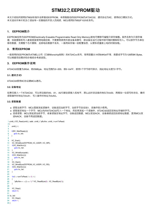
STM32模拟iic驱动eeprom24c128
void IIC_Init(void) //IIC初始化函数
{
GPIO_InitTypeDef GPIO_InitStructure;
RCC_APB2PeriphClockCmd(RCC_APB2Periph_GPIOE, ENABLE);
//使能GPIOB时钟
GPIO_InitStructure.GPIO_Pin = GPIO_Pin_2|GPIO_Pin_3;
GPIO_InitStructure.GPIO_Mode = GPIO_Mode_Out_PP; //推挽输出
GPIO_InitStructure.GPIO_Speed = GPIO_Speed_50MHz;
GPIO_Init(GPIOE, &GPIO_InitStructure);
GPIO_SetBits(GPIOE,GPIO_Pin_2|GPIO_Pin_3); //PE2,PE3 输出高
}
void IIC_Start(void) //IIC开始函数
{
SDA_OUT(); //sda线输出
IIC_SDA=1;
IIC_SCL=1;
delay_us(5);
IIC_SDA=0;//START:when CLK is high,DATA change form high to low
delay_us(5);
IIC_SCL=0; //钳住I2C总线,准备发送或接收数据}
void IIC_Stop(void) //IIC停止函数
{
SDA_OUT();//sda线输出
IIC_SCL=0;
IIC_SDA=0;//STOP:when CLK is high DATA change form low to high
delay_us(5);
IIC_SCL=1;
IIC_SDA=1;//发送I2C总线结束信号
delay_us(5);
}
u8 IIC_Wait_Ack(void) //等待应答
{
u8 ucErrTime=0;
SDA_IN(); //SDA设置为输入
IIC_SDA=1;
delay_us(5);
IIC_SCL=1;
delay_us(1);
while(READ_SDA)
{
ucErrTime++;
if(ucErrTime>250)
{
IIC_Stop();
return 1;
}
}
IIC_SCL=0;//时钟输出0
return 0;
}
void IIC_Ack(void) //SDA输出低电平,IIC应答{
IIC_SCL=0;
SDA_OUT();
IIC_SDA=0;
delay_us(2);
IIC_SCL=1;
delay_us(4);
IIC_SCL=0;
}
void IIC_NAck(void) //SDA输出高电平,IIC非应答{
IIC_SCL=0;
SDA_OUT();
IIC_SDA=1;
delay_us(2);
IIC_SCL=1;
delay_us(4);
IIC_SCL=0;
}
void IIC_Send_Byte(u8 txd) //IIC发送一个字节{
u8 t;
SDA_OUT(); //数据线输出模式
IIC_SCL=0; //拉低时钟开始数据传输
for(t=0;t<8;t++)
{
IIC_SDA=(txd&0x80)>>7;
txd<<=1;
delay_us(5); //对TEA5767这三个延时都是必须的
IIC_SCL=1;
delay_us(5);
IIC_SCL=0;
delay_us(5);
}
}
u8 IIC_Read_Byte(unsigned char ack) //IIC读取一个字节{
unsigned char i,receive=0;
SDA_IN();//SDA设置为输入
for(i=0;i<8;i++ )
{
IIC_SCL=0;
delay_us(5);
IIC_SCL=1;
receive<<=1;
if(READ_SDA)
{
receive++;
}
delay_us(5);
}
if (!ack)
IIC_NAck();//发送nACK
else
IIC_Ack(); //发送ACK
return receive;
}
void AT24CXX_Init(void) //AT254C128初始化
{
IIC_Init();
}
u8 AT24CXX_ReadOneByte(u16 ReadAddr) //AT24C128读取一个字节
{
u8 temp=0;
IIC_Start();
IIC_Send_Byte(0XA0); //发送写命令
IIC_Wait_Ack();
IIC_Send_Byte(ReadAddr>>8);//发送高地址
IIC_Wait_Ack();
IIC_Send_Byte(ReadAddr%256); //发送低地址
IIC_Wait_Ack();
IIC_Start();
IIC_Send_Byte(0XA1); //进入接收模式
IIC_Wait_Ack();
temp=IIC_Read_Byte(0);
IIC_Stop(); //产生一个停止条件
return temp;
}
void AT24CXX_WriteOneByte(u16 WriteAddr,u8 DataToWrite) {
IIC_Start();
IIC_Send_Byte(0XA0); //发送写命令
IIC_Wait_Ack();
IIC_Send_Byte(WriteAddr>>8);//发送高地址
IIC_Wait_Ack();
IIC_Send_Byte(WriteAddr%256); //发送低地址
IIC_Wait_Ack();
IIC_Send_Byte(DataToWrite); //发送字节
IIC_Wait_Ack();
IIC_Stop();//产生一个停止条件
delay_ms(20);
}
u8 AT24CXX_Check(void)
{
u8 temp;
temp=AT24CXX_ReadOneByte(12333);//避免每次开机都写AT24CXX
if(temp==0X55)
{
return 0;
}
else//排除第一次初始化的情况
{
AT24CXX_WriteOneByte(12333,0X55);
temp=AT24CXX_ReadOneByte(12333);
if(temp==0X55)
{
return 0;
}
}
return 1;
}
void AT24CXX_Read(u16 ReadAddr,u8 *pBuffer,u16 NumToRead) {
while(NumToRead)
{
*pBuffer++=AT24CXX_ReadOneByte(ReadAddr++);
NumToRead--;
}
}
void AT24CXX_Write(u16 WriteAddr,u8 *pBuffer,u16 NumToWrite) {
while(NumToWrite--)
{
AT24CXX_WriteOneByte(WriteAddr,*pBuffer);
WriteAddr++;
pBuffer++;
}
}
BY MaiLaoDie。