4520模块中文操作手册
ADR4520_4525_4530_4533_4540_4550精密电压源中文技术手册
ADI中文版数据手册是英文版数据手册的译文,敬请谅解翻译中可能存在的语言组织或翻译错误,ADI不对翻译中存在的差异或由此产生的错误负责。如需确认任何词语的准确性,请参考ADI提供 的最新英文版数据手册。
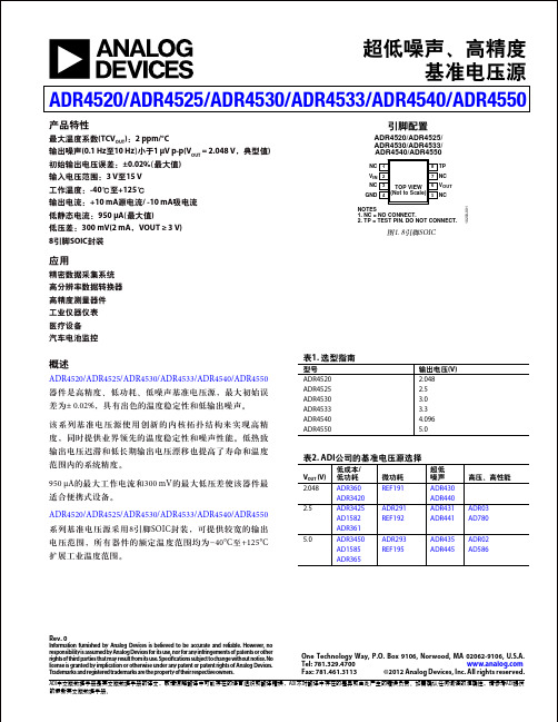
ADR4520/ADR4525/ADR4530/ADR4533/ADR4540/ADR4550
目录
2.048 ADR360
ADAM-4520快速入门手册
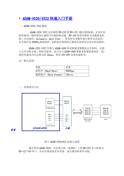
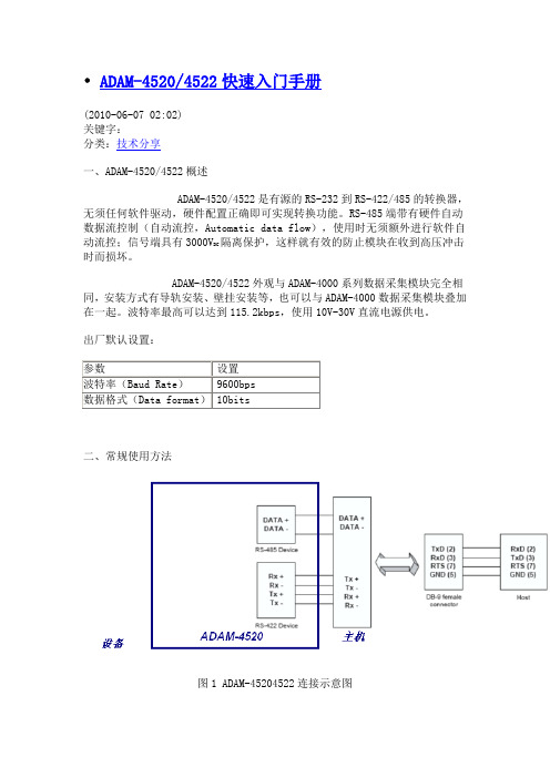
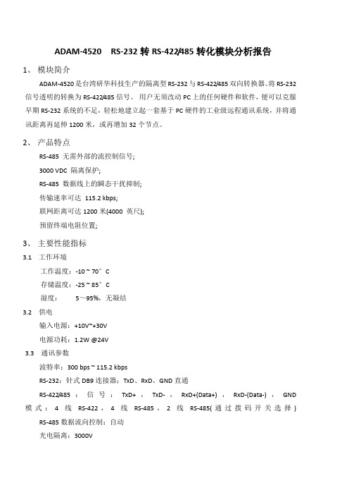
• ADAM-4520/4522快速入门手册一、ADAM-4520/4522概述ADAM-4520/4522是有源的RS-232到RS-422/485的转换器,无须任何软件驱动,硬件配置正确即可实现转换功能。
RS-485端带有硬件自动数据流控制(自动流控,Automatic data flow),使用时无须额外进行软件自动流控;信号端具有3000V隔离保护,这样就有效的防止模块在收到高压冲击时而损坏。
DCADAM-4520/4522外观与ADAM-4000系列数据采集模块完全相同,安装方式有导轨安装、壁挂安装等,也可以与ADAM-4000数据采集模块叠加在一起。
波特率最高可以达到115.2kbps,使用10V-30V直流电源供电。
出厂默认设置:参数 设置波特率(Baud Rate) 9600bps数据格式(Data format)10bits二、常规使用方法图1 ADAM-45204522连接示意图通过使用ADAM-4520,可以将主机(或PLC)上的RS-232串口转换为RS-422/485串口,从而实现连接更多设备、延长通讯距离等功能。
注意:当一对一通讯的时候,也可以反向使用,即将RS-485串口转换为RS-232串口,但是需要注意的是,ADAM-4520/4522无法设置RS-485设备的地址,因此反向使用时仅能用于一对一通讯!三、ADAM-4520/4522使用前必读1. ADAM-4520/4522连接一般PC机时,RS-232端应该使用串口直连线。
由图1可知,一般PC机的DB-9针串口,管脚2为Rx,管脚3为Tx;而4520的管脚2为Tx,管脚3为Rx;根据RS-232需要交叉Rx与Tx的要求,一般PC机与4520连接时使用串口直连线即可。
2. 使用RS-485/422通讯时,需要设置数据格式。
SW1用来设置数据格式,可以是9、10、11、12位(bits)。
默认的数据格式是10bits:1起始位,8数据位,0校验位,1停止位。
三星 SCX-4720F 4520系列数字激光多功能一体机 维修手册

维 修数字激光多功能一体机目 录1注意事项 2参考信息3技术规格 4产品摘要 5拆卸和重新组装 6调整和调节 7故障排除8分解图和零件清单 9框图 10接线图 11原理图数字激光多功能一体机 SCX-4720F 系列 SCX-4720F SCX-4520手 册三星电子本维修手册也在Web 三星电子有限公司的ITSELF 系统上公布http://itself.sec.samsung.co.kr ©三星电子有限公司 2004年7月版本号1.00 代码JC-0127A1注意事项为了防止发生事故并防止损坏设备请在维修打印机之前仔细阅读并严格遵守下列注意事项1.1 安全警告事项1只可由具备合适资格的维修工程师维修本机内的高电压和激光有危险本打印机只应由经过合适培训并具备资格的维修工程师维修2只可使用三星备件打印机内没有需要用户维修的零部件不可擅自改造本打印机或给打印机安装东西否则会造成打印机工作异常并可能触电或起火3激光安全声明在美国打印机经认证符合第1章第J节DHHS 21 CFR针对11类激光产品的要求并且在其他地方本打印机作为I类激光产品经认证符合IEC 825的要求I类激光产品没有危险激光系统和打印机经设计使得在正常操作用户维护或规定的维修条件下人员绝不会受到I类以上激光辐射警告>>在从激光/扫描仪组件拆除防护盖的情况下切勿操作或维修打印机反射光束虽然看不到但会损伤眼睛使用本机时始终应遵循这些基本的安全注意事项以减少起火触电和人员受伤的危险1.2 安全注意事项1.2.1 有毒物质本机含有有毒物质如果摄入会致病1如果LCD控制面板损坏内部液体可能会泄漏该液体有毒应避免与皮肤接触如果溅到眼睛或皮肤上应立即清洗并与医生联系如果液体弄到嘴里或吞下液体应立即找医生医治2勿使小孩接触墨盒墨盒中的墨粉可能有害如果吞下应与医生联系1.2.2 触电和起火安全注意事项如果不遵循下列说明有可能触电或导致起火1只可使用合适的电压否则可能会损坏打印机并可能导致起火或触电2只可使用随打印机附带的电源线使用规格不正确的电线可能造成电缆过热并可能导致起火3电源插座不可过载否则可能导致墙内的电线过热并可能导致起火4不可把水或其它液体弄入打印机中否则可能导致触电不能把曲别针大头针或其他外物落入打印机中否则会造成短路从而导致触电或起火5不要用湿手触摸电源线任一端上的插头否则可能导致触电维修打印机时应从墙上的插座拔下电源插头6插入或拔下电源插头时应小心电源插头必须完全插入否则可能会因接触不良造成过热从而导致起火拔下电源插头时务必牢牢抓住插头拔下7保管好电源线不要扭曲急弯成圆角或以其他方式损坏电源线不可把物体置于电源线之上如果电源线损坏电源线可能会过热并导致起火或者外露的电线可能导致触电立即更换损坏的电源线不可重复使用或修理损坏的电源线一些化学制剂可能会腐蚀电源线的表层使护套变薄或使电线外露从而导致起火或触电8必须保证电源插座和插头不会以任何方式裂开或损坏应立即修复这类缺陷搬动本机时小心不可弄断或损坏电源线或插头9打雷和闪电时小心三星建议预计会出现这类天气时应切断本机的电源如果在这样的天气条件下电源线仍旧接到墙上的插座上则不可触摸本机或电源线10避开潮湿或充满灰尘之处在干净通风良好的场所安装打印机不可把本机置于加湿器附近本机受潮以及本机内部积聚灰尘可能会导致过热并起火11避免打印机受到日光直射否则可能造成打印机内部温度升高导致打印机工作异常在最坏的情况下可能导致起火12不可通过通风机风扇或机箱的其他部位把任何金属物体插入本机中金属物体可能接触本机内部的高压导体并导致触电1.2.3 搬运注意事项下列说明是为了保证人员自身安全以防受伤和损坏打印机1必须保证把打印机安装在平坦能够支承打印机重量的表面上否则打印机会倾斜掉下来2打印机内有许多辊子齿轮和风扇应格外小心保证不会把手指头发或衣服卷入任何旋转设备中3不可在打印机附近放置任何小金属物体水化学制剂或其他液体的容器如果溅出可能流入本机内部损坏本机或触电或起火4不可把本机安装在潮湿或充满灰尘之处敞开的窗户旁边或加湿器或加热器附近在这些地方可能会造成打印机损坏5不可把蜡烛点着了的香烟等置于本机之上否则可能会起火1.2.4 组装/拆卸注意事项小心更换零件始终应使用三星零件拆除本机的任何零件之前小心注意零件和电缆布线的位置必须保证正确装回所有零件和电缆在拆卸打印机或更换任何零件之前应完成下列步骤1检查本机存储器存储的内容并记录用户设置如果更换主板或网卡将删除所有信息2必须保证在维修或更换任何电气零件之前断开电源3断开打印机接口电缆和电源线4只可使用核准的备件必须保证件号产品名称任何额定电压电流或温度正确无误5拆下或装上任何零件时不可过分用力特别是当把螺钉拧入塑料时更应注意6小心不要让任何小零件掉入打印机中7处理硒鼓-如果硒鼓受到光线照射硒鼓可能会损坏无法修复小心不要让硒鼓受到日光或荧光灯或白炽灯室内照明装置直射照射5分钟就可能破坏表面的光电导性质并且导致打印质量下降维修打印机时应格外小心取出硒鼓并存放于黑色袋子或其他避光容器中当在外盖特别是顶盖打开的情况下工作时因光线会射入硒鼓区并可能损坏硒鼓所以要小心-小心不可划伤硒鼓的绿色表面如果划伤或触摸了硒鼓盒上的绿色表面打印质量会受到影响1.2.5 无视本警告可能会使身体受伤1小心一些零件可能发烫定影单元工作温度很高当在打印机上工作时要小心等定影单元冷却下来再拆卸2小心不可卷入手指或头发使用打印机时要小心本机包括许多旋转零件保证不会把手头发衣服等卷入机构中否则可能会导致受伤3搬动打印机时本打印机重15.6kg包括墨盒和纸盒采用安全的抬起和搬运方法使用本机每一侧上的抬起把手如果抬起时不小心可能会使背部受伤4保证安全安装打印机本打印机重15.6Kg保证把打印机安装在平稳能够支承其重量之处否则可能使打印机倾翻或掉下来使身体受伤或损坏打印机5不要把打印机安装在倾斜或不平稳的表面上安装后再次检查打印机是否稳定1.3 静电敏感器件注意事项某些半导体器件可能易于受到静电损伤这些元件通常称为静电敏感ES 器件ESDESD的典型实例有集成电路一些场效应晶体管和半导体芯片元件应当遵守下列方法以减少由静电引起的元件损坏事故小心>>不可向底板或电路通电并遵守所有其它安全注意事项1在即将安装半导体或配有半导体的组件之前触摸已知的接地点放掉身体上的静电另外应佩戴市场上可以买到的腕带装置出于人身安全的原因测试时在对设备通电之前务必除去腕带装置2 拆除配有ESD 的电气组件以后将组件置于导电表面上如铝或铜箔或导电泡沫塑料以防止电荷在组件附近积聚3焊接或熔开ESD 时只能使用接地电烙铁4 只能使用抗静电焊料去除装置一些焊料去除装置未归入抗静电一类中可能产生电荷足以损坏ESD5禁止使用氟利昂推进化学制剂喷射时这些药品可能产生电荷足以损坏ESD6 只有在准备安装之前才可以将替代ESD 从保护包装上取下大多数替代ESD使用导线包装所有导线通过导电泡沫塑料铝箔或类似的导电材料以短路方式接在一起7 在即将从替代ESD 的引线上除去保护短接材料之前触摸安装器件的底板或电路组件的防护材料 8在ESD 和安装ESD 的组件之间保持连续电气接触直到完全插入或焊入电路9 处理散装替代ESD 时尽量减少身体移动通常的运动如衣服纤维摩擦或从铺有地毯的地板上抬起脚时都可能产生静电足以损坏ESD1.4 超级电容器和锂电池注意事项1更换超级电容器或锂电池时应小心如果安装错误可能有爆炸危险并因此而造成人员伤亡和或设备损坏2 务必用制造商推荐的相同或同类电池更换3超级电容器或锂电池含有有毒物质不应打开压碎或焚烧进行处理4依据制造商的说明处理用过的电池3技术规格技术规格在印刷时正确无误产品规格可能有变动恕不另行通知产品规格见下表3.1 通用规格项目SCX-4520 SCX-4720F主要功能复印机打印扫描自动进稿器扫描至电子邮件通过SmarThru软件直接打印扫描至USB存储器传真复印机打印扫描自动进稿器扫描至电子邮件通过SmarThru软件直接打印扫描至USB存储器尺寸宽*深*高不带电话听筒 450mm423mm456mm 17.716.718”净重包括墨盒15.6 kg净重不包括墨盒14.8 kg毛重带包装20.4 kg液晶显示屏16*2 CharI/O接口 USB2.0高速MPU SPGPm/166MHz 打印操作370W休眠模式 30W符合节能之星标准功耗电源开关有输入电压低电压110~127VAC电源输入频率高电压220~240VAC打印54 dBA复印55 dBA噪音待机33 dBA预热时间从冷机状态不到42秒每月最大打印 15,000页用量扫描 1,000页负载周期自动进稿器 1,000页每月平均打印量 1,500页机器使用寿命机器使用寿命 150,000页项 目SCX-4520SCX-4720F拾取辊 150,000页垫组件托盘150,000页垫组件自动进稿器20,000页转印辊 60,000页 定期更换件定影单元 80,000页运行 10~32 环境 温度 不运行 -20~40运行 20~80% 湿度 不运行10~90%海拔 最大8,200英尺 EMI 批准B 类标准/最大 32MB/160MB 标准/最大12MB PS +4MB 传真+2MB系统+2MB 扫描=20MB类型SDRAM SDRAM DIMM -选装DIMM 163264128MB SDRAM扩展存储槽类型-100针SDRAM DIMM 只使用专业本打印机制造的三星存储器零件设备存储器压缩技术 有3.2 打印规格项目SCX-4520 SCX-4270F 打印速度最大22 ppm/Ltr, 20ppm/A4600 dpi打印仿真 GDI PCL6PCL5e PostScript 3级选装*韩国KS/KSSM/KSC5895自动仿真检测有类型 45可升级1位图字体数量N/A省电有5/10/15/30/45分正常 600600 dpi分辨率RET 有12001200 dpi省墨有CP上没有专用按钮存储器16 MB从待机状态约10秒激光扫描器开A4FPOT从冷机状态不到50秒双面打印无打印区 208273 mm Letter打印半色调灰度等级 128级3.3 扫描规格项 目SCX-4520 SCX-4720F 扫描方法 彩色CCD 线条 约75秒USB1.1 灰色 约75秒USB1.1扫描速度 通过自动进稿器 彩色 约150秒USB1.1线条 约75秒USB1.1灰色 约75秒USB1.1扫描速度 通过压盘 彩色 75dpi/300dpi约150秒USB1.1 *USB1.1300dpi Letter 规格Pentium 41.x GHz 12MB RAM 光学600*1200 dpi 分辨率 增强4800dpi*4800dpi 半色调 256级 最大文件宽度 最大216mm 8.5”扫描尺寸 有效扫描宽度 最大208mm 8.2英寸扫描到 电子邮件图像OCR 传真WEB-->通过PC直接扫描至USB 存储器标准彩色 24位扫描扫描深度 单色 线条1位灰度等级8位3.4 复印规格项 目SCX-4520 SCX-4720F文本 600300 dpi 文本/照片 600300 dpi 照片 压盘600600 dpi复印质量选择或原图像类型选择模式 其他N/A待机约10秒压盘约15秒自动进稿器FCOT从冷机状态 50秒SDMC 在所有模式下 22 cpm/Ltr, 20cpm/A4MDMC 在文本模式下600300 dpi14 cpm 复印速度/Letter MDMC 在照片模式下600600 dpi8 cpm 压盘 左后侧原点对正 自动进稿器 居中分辨率 扫描600300 dpi 600600 dpi打印600600 dpi缩放范围 压盘25%至400%自动进稿器25%至100% 多页复印1~99 预设 有 黑度控制 3级通过LED 复印模式=质量 文本混合照片 自动分页复印 600300 dpi 有 自动返回默认模式 有可以改变时间153060180秒关闭 可变默认模式 对比度图像缩小/放大复印份数 每张N 页复印 每张2页每张4页自动分页复印 有仅限于自动进稿器 自动调整复印 有仅限于压盘 双面复印 有仅限于压盘在一页上复印两面打印的原文件例如身份证复印克隆 有仅限于压盘 复印特殊复印 海报 有仅限于压盘项 目SCX-4520SCX-4720F电话听筒 无 无 免提拨号 无 有 查找无 有 (电话簿)一键打出 无 40EA (20换档)*202专用键速拨无 200个位置(00~199)包括一键打出TAD I/F 无 有 音调/脉冲 无 在技术模式中可选择 暂停无 有 自动重拨无 有 重拨上次号码 无 有 特色铃声 无 有 呼叫者ID无 无 外部电话接口无 有 发送/接收日志 无 有 确认无 有 帮助列表无 无 自动拨号列表 无 有报告和列表打印输出 系统数据列表 无 列出所有用户设置 铃声音量 无 有(关闭低中高) 按键音量 无 有(打开关闭) 报警音量 无 有(打开关闭)电话声音控制扬声器无有(打开关闭Comm)3.5 传真技术规格项 目 SCX-4520SCX-4720F兼容性 无ITU-T G3 通信系统无PSTN/PABX 调制解调器速度 无33.6 Kbps 发送速度 无 3秒压缩无MH/MR/MMR/JPEG 彩色传真 无 有仅限于发送 ECM 无 有标准无203 x 98 dpi 精细 无203 x 196 dpi 分辨率 超精无300 x 300 dpi 扫描速度 标准无 2.5秒/LTR (自动进稿器) 精细/超精 无 5秒/LTR 接收传真双面打印输出 无 无多页扫描速度 无 14 ppm/LTR 标准模式 接收模式无 传真TEL Ans/传真DRPD容量无4 MB 选配内存无 无1组拨号最多存储位置 无 199个位置 传真转发 无 有 (打开/关闭) 广播 无 多达209个地点 封面页 无 有 延迟传真 无 有 存储器接收 存储器接收无 有 语音要求无 无 TTI 无 有 RTI 无 有 轮询无 无 接地/二次呼叫 无 无 自动压缩无 有 功能 软件远程升级无 有 电传广告屏障 无 有 安全接收 无 有传真备用存储器无有最长43小时3.6 其他规格项目SCX-4520 SCX-4720F 选项有标准协议SPX/IPX, TCP/IP, Ethertalk, SNMP, HTTP 1.1, DLC/LLC 网络操作系统MS Windows 98/2000/XP/NT/Me, MAC仅限于英文无状态监视功能仅限于Web下载主盘 250页容量20 lbs旁路 50页选装纸盒 250页纸张处理输出容量面向下150页/20lb面向上1页输出控制面向下/面向上主盘A4, Letter, Legal, Folio, Executive, B5纸张幅面旁路旁路Envelopes 63/4, 73/4, #9, #10, DL, C5, B5 纸张重量主盘16~24 lb旁路16~43 lb标准输出从下至上正面FIFO纸张路径直通输出面向上单页最大 216356mm8.5”14”纸张尺寸最小 76127mm3”5”纸张重量12.5 ~ 28lb容量 50页文件宽度 142mm~216mm 5.6”-8.5”自动进稿器文件长度 148mm~356mm 5.8”-14.0”纸盒第二个进纸器1/2000卡纸率自动进稿器1/1000纸盘第二个进纸器1/1000多页进纸率自动进稿器1/500顶边 1.5/177.8mm第一个托盘2.0/177.8mm第二个托盘打印歪斜侧边 2/243.5mm第一个托盘2.5/243.5mm第二个托盘顶边 2.5/190mm第一个托盘3.0/190mm第二个托盘纸张处理续复印歪斜侧边 3.5/277mm第一个托盘4.0/277mm第二个托盘项目SCX-4520 SCX-4720FDOS 无Win 3.x 无Win 95 无Win 98 有Win ME 有Win NT 4.0 有Win 2000 有Win XP 有Mac 仅限于Web版兼容性Linux 无WHQL 多功能一体机有适用于2000&XP打印机 GDI PCL6PCL5e标准PostScript 3级标准TWAIN 有WIA 有RCP 有软件驱动程序PC-FAX 无通过PC调制解调器和传真软件类型一件型如何安装前门打开在前面安装使用寿命最初3K页5% ISO测试图运行标准3K页大打印量5K页墨粉杆传感器无消耗品墨粉计数有点计数器4产品摘要本章叙述主要部件的功能和工作原理4.1 打印机部件4.1.1 正视图4.1.2 后视图*未随机器提供无线网络天线该天线是必须单独购买和安装的选装件选配功能**机器上未作为标准配置配备网络端口您可以单独购买并安装选装网卡***如果贵国有不同的电话连接系统可封上本插孔4.1.3 控制面板SCX-4720F用于保存常拨传真号码并且按下几次按钮即可拨号1可以把一键打出按钮移到编号21至402扫描可以调用可接收扫描图像的PC 软件程序的列表必须使用随本机附带的三星软件打印机设置实用程序创建扫描列表同样可在USB 闪存驱动器中扫描和保存文件并在把该驱动器插入本机的USB 端口时管理该驱动器见用户手册第10章安装USB 闪存驱动器调节当前复印作业文件亮度 为当前复印作业选择文件类型选择复印份数允许您使用特殊复印功能如克隆自动分页自动适合一页双面一纸2页/4页一纸多页和海报复印3复印使复印件比原件小或大在操作期间显示当前状态和提示4在墨盒没有墨粉时打开5用于滚动所选菜单项的可选选项在显示屏上确认选择进入菜单模式并滚动可用菜单返回到上一级菜单随时停止操作在待机模式清除/取消复印选项如黑度文件类型设置复印大小和复印份数5开始一个作业6 拨打一个号码或输入字母数字字符对于当前传真作业调整文件分辨率允许发送传真到多个目的地可把常拨传真号码存为使用一位或两位速拨号码或组拨号码以备自动拨号并可编辑存储的号码还可打印电话簿列表在待机模式下重拨上次拨打的号码或在编辑模式下在传真号中插入暂停符7传真接通电话线8当USB闪存驱动器插入本机正面的USB端口时可以直接打印存储在USB闪存驱动器上的文件允许您通过使用较少的墨粉打印一份文件来节省墨粉9节省允许您通过在预设节省长途电话费时间发送传真来节省电话费用例如使用该功能您可利用夜间较低的长途电话费率控制面板SCX-4520调节当前复印作业文件亮度 1为当前复印作业选择文件类型2扫描可以调用可接收扫描图像的PC 软件程序的列表必须使用随本机附带的三星软件打印机设置实用程序创建扫描列表同样可在USB 闪存驱动器中扫描和保存文件并在把该驱动器插入本机的USB 端口时管理该驱动器见用户手册第10章安装USB 闪存驱动器在操作期间显示当前状态和提示3在墨盒没有墨粉时打开用于滚动所选菜单项的可选选项在显示屏上确认选择进入菜单模式并滚动可用菜单4返回到上一级菜单随时停止操作在待机模式清除/取消复印选项如黑度文件类型设置复印大小和复印份数4开始一个作业选择复印份数允许您使用特殊复印功能如克隆自动分页自动适合一页双面一纸2页/4页一纸多页和海报复印 5使复印件比原件小或大6允许您通过使用较少的墨粉打印一份文件来节省墨粉7当USB 闪存驱动器插入本机正面的USB 端口时可以直接打印存储在USB 闪存驱动器上的文件4.2系统布局SCX-4720F/4520大致由主控制部分操作面板部分扫描仪部分线路接口部分和电源部分组成各部分为单独分开的模块侧重于不同类型产品的共同和标准设计主控制部分采用传真和激光打印机专用控制器由2个CPU和1个电路板组成扫描仪部分由自动进稿器组成通过线束与主控制部分连接4.2.1 进纸选择配有自动盛放纸张的通用纸盒和每次进纸一页的手动进纸器纸盒配有摩擦垫摩擦垫把纸张分开以保证单页进纸并且纸盒具有传感器用于检查纸盘是否空了-进纸方法通用纸盒型-进纸标准中央装入-进纸容量纸盒-250页75 g/m220lb标准纸张手动进纸1页纸OHP信封等等-纸张检测传感器光电传感器-纸张幅面传感器无4.2.2 转印组件该组件包括PTL预转印灯和转印辊PTL向硒鼓发射光使硒鼓表面的电流降低并提高转印效率转印辊把硒鼓表面的墨粉转印到纸上- 使用期限打印60,000页以上15~30中4.2.3 传动组件- 该组件为齿轮传动动力装置电动机向进纸组件定影组件和墨盒提供动力4.2.4 定影组件定影单元- 定影单元包括加热灯加热辊压力辊热敏电阻和控温器该组件利用压力和加热把墨粉粘附到纸张上完成打印作业4.2.4.1 调温装置控温器控温器为温度检测装置当加热灯或加热辊过热时该装置切断加热灯电源以防过热或起火4.2.4.2 温度检测传感器热敏电阻热敏电阻检测加热辊表面温度该信息被传送到主处理器主处理器使用该信息调节加热辊温度4.2.4.3 加热辊加热灯加热加热辊表面当纸张从加热辊和压力辊之间通过时熔化墨粉并把墨粉永久固定到纸张上辊子表面涂有聚四氟乙烯这样可保证墨粉不会粘到辊子表面上4.2.4.4 压力辊压力辊装于加热辊正下方由硅树脂制成辊子表面涂有聚四氟乙烯这样可保证墨粉不会粘到辊子表面上4.2.4.5 安全功能预防过热-第一个防护装置过热时硬件切断-第二个防护装置过热时软件切断-第三个防护装置控温器切断灯电源安全设备-前盖打开时切断定影单元的供电-前盖打开时切断激光扫描器的供电-定影单元盖的表面温度保持在80以下以保护使用者并且在打开后盖时客户易于发现之处粘贴警告标签4.2.5 扫描仪通过感光传感器读取图像扫描仪包括CCD模块连接板自动进稿器板AFE (模拟前端)和图像处理器(位于CPU中)压盘玻璃和自动进稿器机构• CCD模块规格1. 分辨率600dpi/A42. 最大扫描宽度8.5”3. 滤色器红色绿色蓝色4. 输出通道3个通道(R, G, B)5. 有效像素5,400个像素*36. 电压24V & 5V7. 预热时间最多30秒(70%光到达)8. 灯使用寿命30,000小时(25o C)• 图像处理器规格1. 工作频率 66MHz2. 图像传感器接口200/300/600 dpi CIS或CCD3. 行时间复印传真二进制(Lineart, 半色调) PC扫描 1.5毫秒/行彩色PC扫描(灰色256彩色真彩色) 4.5毫秒/行4. A/D转换10位转换4.2.6 LSU激光扫描器激光扫描器是激光打印机的核心部件该组件把从计算机上接收的视频数据转换为OPC鼓表面上的静电潜像通过控制激光束并让激光照射OPC鼓表面可实现这一点旋转多棱镜把激光反射到OPC上并且多棱镜的一面为扫描的一行OPC鼓以纸张速度旋转把图像扫描到页面上当激光扫描器的激光束到达多棱镜的末端时产生/HSYNC信号并把该信号发送到控制器控制器检测/HSYNC信号以便在纸张上调节图像的竖线换句话说检测到/HSYNC信号后把图像数据发送到激光扫描器从而在纸张上调节左边4.2.7 墨盒在墨盒中OPC组件和墨粉组件合为一体OPC组件有OPC鼓和充电辊而墨盒组件有墨粉供墨辊显影辊和刀片刮墨刀-显影方法非磁性单元件接触方法-墨粉非磁性单元件粉状墨粉-墨粉使用期限3,000页IDC图/标准A4-墨粉剩余量检测传感器有-OPC清理静电方法-管理废弃墨粉使用清理刀收集墨粉-OPC鼓保护罩有-墨盒分类设备按中断机架通道给ID分类4.3 主要印刷电路板组件引擎板和控制器板合为一体从功能方面来说该板包括CPU 打印机扫描仪和行控制功能CPU 起总线控制器I/O处理器电动机驱动电路和PC 接口的作用主板把当前图像视频数据发送到激光扫描器并管理电子照像打印过程PBA 驱动电路包括主电动机进纸墨盒定影单元驱动电路离合器驱动电路预转印灯驱动电路加热灯驱动电路CIS驱动电路扫描电动机驱动电路调制解调器和风扇驱动电路进纸卡纸传感器和缺纸传感器发出的信号从电源PBA 直接输入主板1图像处理器CIP4E U10 11 电动机驱动电路TEA37185U521 线路转发器74LVX161284U362 处理器ASIC SPGPm U35 12 电动机驱动电路TEA37185U922 VEDIC X-TAL 19.6MHzOSC33 闪存代码-高电平29LV160DB U2313 USB 2.0 NET 2272 U50 23 CPU X-TAL 12MHz OSC84 闪存代码-低电平29LV160DB U3014 CMOS 逻辑74HCT273U58 24 调制解调器X-TAL28.224MHz OSC65 闪存 PCL6-高电平29LV160DB U2415 CMOS 逻辑74HCT273U5925 主USB X-TAL 6MHz OSC96 闪存 PCL6-低电平29LV160DB U3116 松夏3V BAT226 PS3 DIMM CN127 SDRAM K4S281632E U4517 VARTA 3.6V BAT127 RAM DIMM CN12 8 SDRAM K4S281632EU4618 FPGA EX64-FTQ64U44 28 插口USB JI 9 调制解调器FM336U62 19 A/D 变换器AFE-CIP4E U3 29 插口DIN CN17 10 SRAM K6R1016VID U220 主USB TDOTG242U14830。
FLUKE54200中文操作指南
FLUKE54200中文操作指南仪器的设定和检查 开机之后, 仪器自动地被设定为上一次关机之前的设置。
例如:图3-1. 主菜单按standard 软键(F1) 出现选定国家的省缺设置子菜单,例如,英国图3-2. 该国家的视频标准和伴音制式按edit 软键(F3) 弹出预先定义的国家目录列表菜单 按↑或者↓软键(F1或者F2)选择国家,例如,德国。
如果你需要的国家没有被列出, 就选择一个和你要使用的国家相同或相似的视频标准和伴音制式。
图3-3. 预先定义的国家目录列表菜单按enter 软键(F5)确认你的选择 屏幕显示出你所选择国家的视频标准和伴音制式图3-4. 所选国家的视频标准和伴音制式 如果你的电视机不支持该制式,可以通过按↑或者↓软键(F1或者F2)来选择你所需要的视频标准和伴音制式,例如,FM Germany按edit 软键(F3)按↑或者↓软键(F1或者F2)来选择你所需要的标准和伴音制式,例如,FM Mono按enter 软键(F5)确认你的选择再按enter 软键(F5)回到主菜单图3-5. 设定后的主菜单检查video(视频) 和 chroma(色度) 的幅度是否设置为 100%如果不是,按video 软键(F2),屏幕显示出video(视频)子菜单当前所有的设置。
图3-6. video(视频)子菜单当前的设置按edit 软键(F3)弹出一个可以输入数字的菜单图3-7. video(视频)幅度设置 使用数字按键输入100 按enter 软键(F5)确认你的输入 按↑软键(F2)来选择chroma(色度)使用数字按键输入100 按enter 软键(F5)确认你的输入 再按enter 软键(F5)回到主菜单图3-8. 改变设置后的主菜单按显示屏右边的FREQ 键,选择适当的射频载波频率,例如,203.25 MHz 弹出一个数字输入菜单图3-9. 载波频率设置使用数字按键输入203.25按enter 软键(F5)确认你的输入图3-10. 选定载波频率将你的电视机设置为相同的频率或相应的电视频道,在这个例子里,是9频道。
THS4520中文资料
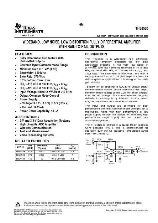
FEATURES DESCRIPTIONAPPLICATIONSRELATED PRODUCTSFrom50W0.2249.9WestTHS4520SLOS503A–SEPTEMBER2006–REVISED OCTOBER2006 WIDEBAND,LOW NOISE,LOW DISTORTION FULLY DIFFERENTIAL AMPLIFIERWITH RAIL-TO-RAIL OUTPUTS•Fully Differential Architecture With The THS4520is a wideband,fully differential Rail-to-Rail Outputs operational amplifier designed for5-V dataacquisition systems.It has very low noise at •Centered Input Common-mode Range2nV/√Hz,and low harmonic distortion of–115dBc •Minimum Gain of1V/V(0dB)HD2and–123dBc HD3at100kHz with8V PP,and •Bandwidth:620MHz1-kΩload.The slew rate is570V/µs,and with asettling time of7ns to0.1%(2-V step),it is ideal for •Slew Rate:570V/µsdata acquisition applications.It is designed for unity •0.1%Settling Time:7nsgain stability.•HD2:–115dBc at100kHz,V OD=8V PPTo allow for dc coupling to ADCs,its unique output •HD3:–123dBc at100kHz,V OD=8V PPcommon-mode control circuit maintains the output •Input Voltage Noise:2nV/√Hz(f>10kHz)common-mode voltage within0.25mV offset(typical)from the set voltage.The common-mode set point •Output Common-Mode Controldefaults to mid-supply by internal circuitry,which •Power Supply:may be over-driven from an external source.–Voltage:3.3V(±1.5V)to5V(±2.5V)The input and output are optimized for best –Current:14.2mAperformance with their common-mode voltages set to •Power-Down Capability:15µA mid-supply.Along with high performance at lowpower supply voltage,this makes for extremely highperformance single supply5-V and 3.3-V dataacquisition systems.•5-V and3.3-V Data Acquisition Systems•High Linearity ADC Amplifier The THS4520is offered in a Quad16-pin leadlessQFN package(RGT),and is characterized for •Wireless Communicationoperation over the full industrial temperature range •Test and Measurementfrom–40°C to85°C.•Voice Processing SystemsBW Slew Rate THD V NDevice(MHZ)(V/µsec)(dBc)(nV/Hz)THS450920006600-102at10MHz 1.9THS45003702800-82at8MHz7THS413015052-97at250kHz 1.3Please be aware that an important notice concerning availability,standard warranty,and use in critical applications of TexasInstruments semiconductor products and disclaimers thereto appears at the end of this data sheet.PRODUCTION DATA information is current as of publication date.Copyright©2006,Texas Instruments Incorporated Products conform to specifications per the terms of the TexasInstruments standard warranty.Production processing does notnecessarily include testing of all parameters.DISSIPATION RATINGS TABLE PER PACKAGETHS4520SLOS503A–SEPTEMBER 2006–REVISED OCTOBER 2006This integrated circuit can be damaged by ESD.Texas Instruments recommends that all integrated circuits be handled with appropriate precautions.Failure to observe proper handling and installation procedures can cause damage.ESD damage can range from subtle performance degradation to complete device failure.Precision integrated circuits may be more susceptible to damage because very small parametric changes could cause the device not to meet its published specifications.over operating free-air temperature range (unless otherwise noted)UNITV S–to V S+Supply voltage 6V V I Input voltage±V S V ID Differential input voltage 4V I OOutput current (1)200mAContinuous power dissipationSee Dissipation Rating TableMaximum junction temperature150°C T J Maximum junction temperature,continuous operation,long term reliability 125°C T A Operating free-air temperature range –40°C to 85°C T stgStorage temperature range–65°C to 150°CLead temperature 1,6mm (1/16inch)from case for 10seconds300°C HBM2000ESD ratingsCDM 1500MM100(1)The THS4520incorporates a (QFN)exposed thermal pad on the underside of the chip.See TI technical brief SLMA002and SLMA004for more information about utilizing the QFN thermally enhanced package.POWER RATINGPACKAGE (1)θJC θJA T A ≤25°C T A =85°C RGT (16)2.4°C/W39.5°C/W2.3W225mW(1)For the most current package and ordering information,see the Package Option Addendum at the end of this document,or see the TI Web site at .2Submit Documentation FeedbackDEVICE INFORMATIONV V PD V IN+V OUT−CMV S−V S+THS4520SLOS503A–SEPTEMBER 2006–REVISED OCTOBER 2006RGT Package (TOP VIEW)TERMINAL FUNCTIONSTERMINAL (RGT PACKAGE)DESCRIPTION 1NC No internal connection 2V IN–Inverting amplifier input 3V OUT+Non-inverted amplifier output 4,9CM Common-mode voltage input 5,6,7,8V S+Positive amplifier power supply input 10V OUT–Inverted amplifier output 11V IN+Non-inverting amplifier inputPowerdown,PD =logic low puts part into low power mode,PD =logic high or open for normal operation.12PD If the PD pin is open (unterminated)the device will default to the enabled state.13,14,15,16V S–Negative amplifier power supply input3Submit Documentation FeedbackSPECIFICATIONS;V S+–V S–=5V:THS4520SLOS503A–SEPTEMBER 2006–REVISED OCTOBER 2006Test conditions unless otherwise noted:V S+=+2.5V,V S–=–2.5V,G =0dB,CM =open,V O =2V PP ,R F =499Ω,R L =200ΩDifferential,T A =25°C Single-Ended Input,Differential Output,Input and Output Referenced to mid-supplyTEST PARAMETERTEST CONDITIONSMINTYPMAXUNITLEVEL (1)AC PERFORMANCEG =0dB,V O =100mV PP620MHz G =6dB,V O =100mV PP 450MHz Small-Signal BandwidthG =10dB,V O =100mV PP 330MHz G =20dB,V O =100mV PP120MHz Gain-Bandwidth Product G =20dB1200MHz Bandwidth for 0.1dB flatness G =10dB,V O =2V PP 30MHz Large-Signal Bandwidth G =10dB,V O =2V PP132MHz Slew Rate (Differential)570V/µsRise Time 4Fall Time2-V Step 4nsCSettling Time to 1% 6.2Settling Time to 0.1%7f =100kHz,V OD =8V PP –115dBc 2nd Order Harmonic Distortion R L =1k Ωf =100kHz,V OD =8V PP–123dBc 3rd Order Harmonic DistortionR L =1k Ω1-kHz Tone Spacing,R L =1k Ω,f C =100kHz –135dBc 3rd Order Intermodulation Distortion V OD =4V PP /Tone Input Voltage Noise f >10kHz 2nV/√Hz Input Current Noise f >10kHz2pA/√Hz DC PERFORMANCEOpen-Loop Voltage Gain (A OL )112dBC T A =25°C±0.25±2.5mV Input Offset Voltage A T A =–40°C to 85°C ±0.25±3mV T A =25°C6.510Input Bias Current µA A T A =–40°C to 85°C 6.411T A =25°C±0.2±2.5Input Offset Current µAAT A =–40°C to 85°C±0.2±3INPUTCommon-Mode Input Range High 1.75V Common-Mode Input Range Low -1.3BCommon-Mode Rejection Ratio84dB(1)Test levels:(A)100%tested at 25°C.Overtemperature limits by characterization and simulation.(B)Limits set by characterization and simulation.(C)Typical value only for information.4Submit Documentation FeedbackTHS4520 SLOS503A–SEPTEMBER2006–REVISED OCTOBER2006SPECIFICATIONS;V S+–V S–=5V:(continued)Test conditions unless otherwise noted:V S+=+2.5V,V S–=–2.5V,G=0dB,CM=open,V O=2V PP,R F=499Ω,R L=200ΩDifferential,T A=25°C Single-Ended Input,Differential Output,Input and Output Referenced to mid-supplyTEST PARAMETER TEST CONDITIONS MIN TYP MAX UNITLEVEL(1) OUTPUTT A=25°C 1.95 2.16Maximum Output Voltage High VT A=–40°C to85°C 1.9 2.16Each output with100Ωto mid-supply TA =25°C–2.16–1.95AMinimum Output Voltage Low VT A=–40°C to85°C–2.16–1.9Differential Output Voltage Swing T A=–40°C to85°C7.88.64VDifferential Output Current Drive R L=10Ω105mAC Output Balance Error V O=100mV,f=1MHz–80dBOUTPUT COMMON-MODE VOLTAGE CONTROLSmall-Signal Bandwidth230MHzGain1V/VOutput Common-Mode Offset1.25V<CM<3.5V±0.25mVfrom CM input CCM Input Bias Current 1.25V<CM<3.5V0.6µACM Input Voltage-1.5 1.5VCM Default Voltage CM=0.5(V S++V S-)0VPOWER SUPPLYSpecified Operating Voltage35 5.25V CT A=25°C14.215.3Maximum Quiescent Current mAT A=–40°C to85°C14.215.5AT A=25°C13.114.2Minimum Quiescent Current mAT A=–40°C to85°C12.7514.2Power Supply Rejection(±PSRR)94dB CPOWERDOWN Referenced to V s–Enable Voltage Threshold>1.5VFor additional information,see the ApplicationCInformation section of this data sheet.Disable Voltage Threshold<-1.5VT A=25°C1570Powerdown Quiescent CurrentµA AT A=–40°C to85°C15755Submit Documentation FeedbackSPECIFICATIONS;V S+–V S–=3.3V:THS4520SLOS503A–SEPTEMBER 2006–REVISED OCTOBER 2006Test conditions unless otherwise noted:V S+=+1.65V,V S–=–1.65V,G =0dB,CM =open,V O =1V PP ,R F =499Ω,R L =200ΩDifferential,T A =25°C Single-Ended Input,Differential Output,Input and Output Referenced to mid-supplyTEST PARAMETERTEST CONDITIONSTYPUNITLEVEL (1)AC PERFORMANCEG =0dB,V O =100mV PP600MHz G =6dB,V O =100mV PP 400MHz Small-Signal BandwidthG =10dB,V O =100mV PP 310MHz G =20dB,V O =100mV PP120MHz Gain-Bandwidth Product G =20dB1200MHz Bandwidth for 0.1-dB flatness G =6dB,V O =1V PP 30MHz Large-Signal Bandwidth G =6dB,V O =1V PPGHz Slew Rate (Differential)520V/µsCRise Time 4Fall Time2-V Step 4nsSettling Time to 1% 6.6Settling Time to 0.1%7.1f =100kHz,V OD =4V PP ,R L =1k Ω–135dBc 2nd Order Harmonic Distortion f =100kHz,V OD =4V PP ,R L =1k Ω–146dBc 3rd Order Harmonic Distortion Input Voltage Noise f >10kHz 2nV/√Hz Input Current Noise f >10kHz 2pA/√Hz DC PERFORMANCEOpen-Loop Voltage Gain (A OL )104dB Input Offset Voltage T A =25°C ±0.25mV CInput Bias Current T A =25°C 6.5µA Input Offset Current T A =25°C±0.2µAINPUTCommon-Mode Input Range High 1.4V Common-Mode Input Range Low -0.45CCommon-Mode Rejection Ratio84dB(1)Test levels:(A)100%tested at 25°C.Overtemperature limits by characterization and simulation.(B)Limits set by characterization and simulation.(C)Typical value only for information.6Submit Documentation FeedbackTHS4520 SLOS503A–SEPTEMBER2006–REVISED OCTOBER2006SPECIFICATIONS;V S+–V S–=3.3V:(continued)Test conditions unless otherwise noted:V S+=+1.65V,V S–=–1.65V,G=0dB,CM=open,V O=1V PP,R F=499Ω,R L=200ΩDifferential,T A=25°C Single-Ended Input,Differential Output,Input and Output Referenced to mid-supplyTEST PARAMETER TEST CONDITIONS TYP UNITLEVEL(1) OUTPUTMaximum Output Voltage High T A=25°C 1.4VEach output with100Ωtomid-supplyMinimum Output Voltage Low T A=25°C-1.4VDifferential Output Voltage Swing 5.6V C Differential Output Current Drive R L=10Ω78mAOutput Balance Error V O=100mV,f=1MHz–80dBOUTPUT COMMON-MODE VOLTAGE CONTROLSmall-Signal Bandwidth224MHzGain1V/VOutput Common-Mode Offset1.25V<CM<3.5V±0.25mV Cfrom CM inputCM Input Bias Current 1.25V<CM<3.5V0.6µACM Default Voltage CM=0.5(V S++V S-)0VPOWER SUPPLYSpecified Operating Voltage 3.3VQuiescent Current T A=25°C13mA C Power Supply Rejection(±PSRR)94dBPOWERDOWN Referenced to V s–Enable Voltage Threshold>1VFor additional information,see the Application Informationsection of this data sheet.Disable Voltage Threshold<-1V C Powerdown Quiescent Current10µA7Submit Documentation FeedbackTYPICAL CHARACTERISTICSTYPICAL AC PERFORMANCE:V S+–V S–=5Vf - Frequency - MHzS i g n a l G a i n - d Bf - Frequency - MHzS i g n a l G a i n - d BTHS4520SLOS503A–SEPTEMBER 2006–REVISED OCTOBER 2006Test conditions unless otherwise noted:V S+=+2.5V,V S–=–2.5V,CM =open,V O =2V PP ,R F =499Ω,R L =200ΩDifferential,G =0dB,Single-Ended Input,Input and Output Referenced to MidrailSmall-Signal Frequency Response Figure 1Large Signal Frequency Response Figure 20.1dB Flatness Figure 3S-Parameters vs Frequency Figure 4Transition Rate vs Output VoltageFigure 5Figure 6Transient Response Figure 7Output Voltage Swing vs Load ResistanceFigure 8Input Offset Voltage vs Input Common-Mode Voltage Figure 9Input Bias Current vs Supply Voltage Figure 10Open Loop Gain vs Frequency Figure 11Input Referred Noise vs Frequency Figure 12Quiescent Current vs Supply VoltageFigure 13Power Supply Current vs Supply Voltage in Powerdown Mode Figure 14Output Balance Errorvs Frequency Figure 15CM Small-Signal Frequency Response Figure 16CM Input Bias Currentvs CM Input Voltage Figure 17Differential Output Offset Voltage vs CM Input Voltage Figure 18Output Common-Mode Offsetvs CM Input VoltageFigure 19SMALL-SIGNALFREQUENCY RESPONSELARGE-SIGNAL FREQUENCY RESPONSEFigure 1.Figure 2.8Submit Documentation Feedback5.65.966.26.5S i g n a l G a i n −d Bf −Frequency −MHz5.55.75.86.16.36.4-90-80-60-40-30-20-1010S -P a r a m e t e r s - d Bf - Frequency - MHz-70-500t −Time −5 ns/divV O D −D i f f e r e n t i a l O u t p u t V o l t a g e −VS l e w R a t e - V /sm 200250300350400450500550600V - Differential Output Voltage - V OD PPt −Time −5 ns/divV O D −D i f f e r e n t i a l O u t p u tV o l t a g e −V0247910R - Load Resistance -L WV V o l t a g e - VO D - D i f f e r e n t i a l O u t p u t 3568THS4520SLOS503A–SEPTEMBER 2006–REVISED OCTOBER 20060.1-dB FLATNESSS-PARAMETERS vs FREQUENCYFigure 3.Figure 4.TRANSITION RATE vs OUTPUT VOLTAGETRANSIENT RESPONSEFigure 5.Figure 6.TRANSIENT RESPONSEOUTPUT VOLTAGE SWING vs LOAD RESISTANCEFigure 7.Figure 8.9Submit Documentation Feedback1.51.72 2.4 2.5V - Supply Voltage -VS ±V I n p u t O f f s e t V o l t a g e -VI O -m 1.6 1.8 2.11.9 2.2 2.333.55.5766.57.51.51.72 2.4 2.5V - Supply Voltage -VS ±I I n p u tB i a s V o l t a g e -AI B -m 1.6 1.8 2.11.9 2.2 2.344.55n V H z−V o l t a g e N o i s e −V n I n −C u r r e n t N o i s e −p A /H z10100f −Frequency −HzO p e n L o o p G a i n −d BO p e n L o o p P h a s e −d e g r e e sf −Frequency −Hz-200-160-120-80-400401010.512.514.51413.5151.51.7522.5V - Supply Voltage -VS ±I - m AQ - Q u i e s c e n t C u r r e n t 2.2511.51213015987101.51.7522.5V - Supply Voltage -VS ±P o w e r S u p p l y -AC u r r e n t m 2.252346THS4520SLOS503A–SEPTEMBER 2006–REVISED OCTOBER 2006INPUT BIAS CURRENTINPUT OFFSET VOLTAGE vs vsINPUT COMMON-MODE VOLTAGESUPPLY VOLTAGEFigure 9.Figure 10.OPEN LOOP GAIN AND PHASE vs FREQUENCYINPUT REFERRED NOISE vs FREQUENCYFigure 11.Figure 12.POWER SUPPLY CURRENT vs SUPPLY VOLTAGE INQUIESCENT CURRENT vs SUPPLY VOLTAGEPOWER-DOWN MODEFigure 13.Figure 14.10Submit Documentation Feedback0.111000f - Frequency - MHzB a l a n c e E r r o r - d B10100f - Frequency - MHzV - S i g n a l G a i n - d BO C M -150-100150100200-2.50.50 2.5V - Common-Mode Input Voltage - VICR C o m m o n -M o d e I n p u t B i a s -AC u r r e n t m 2-50050-2-1.5-1-0.511.5-2.50.50 2.5V - Common-Mode Input Voltage - VICR D i f f e r e n t i a l O u t p u t O f f s e t V o l t a g e - m V2-2-1.5-1-0.51 1.5-7-6324-5-2-1-4-310-2.50.50 2.5V - Common-Mode Input Voltage - VICR O u t p u t C o m m o n -M o d e O f f s e t - m V2-2-1.5-1-0.51 1.5-50-40403050-30010-20-1020SLOS503A–SEPTEMBER 2006–REVISED OCTOBER 2006OUTPUT BALANCE ERROR vs FREQUENCYCM SMALL SIGNAL FREQUENCY RESPONSEFigure 15.Figure 16.DIFFERENTIAL OUTPUT OFFSET VOLTAGE vsCM INPUT BIAS CURRENT vs CM INPUT VOLTAGECM INPUT VOLTAGEFigure 17.Figure 18.OUTPUT COMMON-MODE OFFSET vsCM INPUT VOLTAGEFigure 19.TYPICAL AC PERFORMANCE:V S+–V S–=3.3Vf - Frequency - MHzS i g n a l G a i n - d Bf - Frequency - MHzS i g n a l G a i n - d B5.65.966.26.5S i g n a l G a i n −d Bf −Frequency −MHz5.55.75.86.16.36.46.66.76.86.971-90-80-60-40-30-20-1010S -P a r a m e t e r s - d Bf - Frequency - MHz-70-500SLOS503A–SEPTEMBER 2006–REVISED OCTOBER 2006Test conditions unless otherwise noted:V S+=1.65V,V S–=–1.65V,CM =open,V OD =1V PP ,R F =499Ω,R L =200ΩDifferential,G =0dB,Single-Ended Input,Input and Output Referenced to MidrailSmall-Signal Frequency Response Figure 20Large Signal Frequency Response Figure 210.1dB Flatness Figure 22S-Parameters vs Frequency Figure 23Transition Rate vs Output VoltageFigure 24Figure 25Transient Response Figure 26Output Balance Error vs Frequency Figure 27CM Input Impedancevs FrequencyFigure 28SMALL-SIGNAL FREQUENCY RESPONSELARGE-SIGNAL FREQUENCY RESPONSEFigure 20.Figure 21.0.1dB FLATNESSS-PARAMETERS vs FREQUENCYFigure 22.Figure 23.t −Time −5 ns/divV O D −D i f f e r e n t i a l O u t p u t V o l t a g e −VS l e w R a t e - V /sm 20025030035040045050055060000.51 1.522.533.54V - Differential Output Voltage - V ODPPt −Time −5 ns/divV O D −D i f f e r e n t i a l O u t p u t V o l t a g e −V-90-80-40-30-200.111000f - Frequency - MHzB a l a n c e E r r o r - d B-60-5010100-700.1110100f - Frequency - MHzV - S i g n a l G a i n - d BO C M SLOS503A–SEPTEMBER 2006–REVISED OCTOBER 2006TRANSITION RATE vs OUTPUT VOLTAGETRANSIENT RESPONSEFigure 24.Figure 25.TRANSIENT RESPONSEOUTPUT BALANCE ERROR vs FREQUENCYFigure 26.Figure 27.CM INPUT IMPEDANCE vs FREQUENCYFigure 28.TEST CIRCUITSFrequency ResponseFrom 50W 0.2249.9W estOutput Measured Here With High ImpedanceDifferential ProbeFrom 50W W 0.22F m 49.9WSLOS503A–SEPTEMBER 2006–REVISED OCTOBER 2006Note:The total load includes 50-Ωtermination by the test ponents are chosen to achieve load and 50-Ωline termination through a 1:1The THS4520is tested with the following test circuits transformer.built on the EVM.For simplicity,power supply decoupling is not shown –see layout in the Due to the voltage divider on the output formed by applications section for recommendations.the load component values,the amplifier's output is attenuated in test.The column Atten in Table 2shows the attenuation expected from the resistor divider.When using a transformer at the output the signal will have slightly more loss,and the numbers will be approximate.The general circit shown in Figure 29is modified as shown in Figure 30,and is used to measure the frequency response of the device.Figure 29.General Test Circuit for Device TestingA network analyzer is used as the signal source and and Characterization as the measurement device.The output impedance of the network analyzer is 50Ω.R IT and R G are Depending on the test conditions,component values chosen to impedance match to 50Ω,and to maintain are changed per the following tables,or as otherwise the proper gain.To balance the amplifier,a 0.22-µF noted.The signal generators used are ac coupled capacitor and 49.9-Ωresistor to ground are inserted 50-Ωsources and a 0.22-µF capacitor and a 49.9-Ωacross R IT on the alternate input.resistor to ground are inserted across R IT on the alternate input to balance the circuit.A split power The output is probed using a high-impedance supply is used to ease the interface to common test differential probe across the 100-Ωresistor.The gain equipment,but the amplifier can be operated is referred to the amplifier output by adding back the single-supply as described in the applications section 6-dB loss due to the voltage divider on the output.with no impact on performance.Table 1.Gain Component ValuesGAIN R F R G R IT 0dB 499Ω487Ω53.6Ω6dB 499Ω243Ω57.6Ω10dB 499Ω147Ω63.4Ω14dB 499Ω88.7Ω71.5Ω20dB499Ω34.8Ω115ΩFigure 30.Frequency Response Test CircuitNote:The gain setting includes 50-Ωsource ponents are chosen to achieve gain and 50-Ωinput termination.Table 2.Load Component ValuesR L R O R OT Atten.100Ω25Ωopen 6dB 200Ω86.6Ω69.8Ω16.8dB 499Ω237Ω56.2Ω25.5dB 1k Ω487Ω52.3Ω31.8dBS-Parameter,Slew Rate,Transient Response,CM InputV INFrom 50-SourceW 49.90.22F m V OUT+V OUT–To 50-TestEquipment W 49.90.22F mFrom 50Ω0.22m 49.9OUT+To 50WTestEquipmentOUT−SLOS503A–SEPTEMBER 2006–REVISED OCTOBER 2006Settling Time,Output VoltageThe circuit shown in Figure 32is used to measure The circuit shown in Figure 31is used to measure the frequency response of the CM input.Frequency s-parameters,slew rate,transient response,settling response is measured single-ended at V OUT+or time,and output voltage swing.V OUT–with the input injected at V IN ,R CM =0Ωand R CMT =49.9Ω.Because S21is measured single-ended at the load with 50-Ωdouble termination,add 12dB to see the amplifier’s output as a differential signal.Figure 32.CM Input Test CircuitFigure 31.S-Parameter,SR,Transient Response,Settling Time,V OUT SwingAPPLICATION INFORMATIONAPPLICATIONSDifferential Input to Differential Output AmplifierInputR FOutputV OUT+V OUT–Input Common-Mode Voltage RangeRV OUT+V OUT–V IN–FV IN+÷÷øöççèæ+´+÷÷øöççèæ+´=-+F G F IN F G G OUT IC R R R V R R R V V (1)Single-Ended InputtoDifferentialOutputSetting the Output Common-Mode Voltage SLOS503A–SEPTEMBER 2006–REVISED OCTOBER 2006The following circuits show application information for the THS4520.For simplicity,power supply decoupling capacitors are not shown in these diagrams.For more detail on the use and operation of fully differential op amps see application report Fully-Differential Amplifiers (SLOA054).The THS4520is a fully differential op amp,and can be used to amplify differential input signals to differential output signals.A basic block diagram of Figure 34.Single-Ended Input to Differentialthe circuit is shown in Figure 33(CM input not Output Amplifier shown).The gain of the circuit is set by R F divided by R G .The input common-model voltage of a fully differential op amp is the voltage at the '+'and '–'input pins of the op amp.It is important to not violate the input common-mode voltage range (V ICR )of the op amp.Assuming the op amp is in linear operation,the differential voltage across the input pins is only a few millivolts at most.So finding the voltage at one input pin determines the input common-mode voltage of the op amp.Treating the negative input as a summing node,the voltage is given by Equation 1:Figure 33.Differential Input to Differential OutputAmplifier To determine the V ICR of the op amp,the voltage atthe negative input is evaluated at the extremes of Depending on the source and load,input and output V OUT+.termination can be accomplished by adding R IT and R O .As the gain of the op amp increases,the input common-mode voltage becomes closer and closer to the input common-mode voltage of the source.AmplifierThe THS4520can be used to amplify and convert single-ended input signals to differential output The output common-mode voltage is set by the signals.A basic block diagram of the circuit is shown voltage at the CM pin(s).The internal common-mode in Figure 34(CM input not shown).The gain of the control circuit maintains the output common-mode circuit is again set by R F divided by R G .voltage within 0.25-mV offset (typical)from the set voltage,when set within ±0.5V of mid-supply.If left unconnected,the common-mode set point is set to mid-supply by internal circuitry,which may be over-driven from an external source.Figure 35is representative of the CM input.The internal CM circuit has about 230MHz of bandwidth,which isSingle-Supply Operation (3V to 5V)()W--=-+k 50V V V 2I S S CM EXT (2)VS–Powerdown Operation:DeviceV OUT+V OUT-()÷÷øöççèæ+-÷÷øöççèæ-=+F IN IC FCM S IC PU R 1R 1V R1V V V R (3)SLOS503A–SEPTEMBER 2006–REVISED OCTOBER 2006required for best performance,but it is intended to be a DC bias input pin.Bypass capacitors are To facilitate testing with common lab equipment,the recommended on this pin to reduce noise at the THS4520EVM allows split-supply operation,and the output.The external current required to overdrive the characterization data presented in this data sheet internal resistor divider is given by Equation 2:was taken with split-supply power inputs.The device can easily be used with a single-supply power input without degrading the performance.Figure 36,Figure 37,and Figure 38show DC and AC-coupled single-supply circuits with single-ended inputs.These where V CM is the voltage applied to the CM pin.configurations all allow the input and output common-mode voltage to be set to mid-supply allowing for optimum performance.The information presented here can also be applied to differential input sources.In Figure 36,the source is referenced to the same voltage as the CM pin (V CM ).V CM is set by the internal circuit to mid-supply.R T along with the input impedance of the amplifier circuit provides input termination,which is also referenced to V CM .Note R S and R T are added to the alternate input from the signal input to balance the amplifier.Alternately,Figure 35.CM Input Circuitone resistor can be used equal to the combined value R G +R S ||R T on this input.This is also true of the circuits shown in Figure 37and Figure 38.Enable/Disable ThresholdsThe enable/disable thresholds of the THS4520are dependent upon the power supplies,and the thresholds are always referenced to the lower power supply rail.The device is enabled or disabled for the following conditions:•Device enabled:V PD >V S-+0.8x (V S+-V S-)•Device disabled:V PD <V S-+0.2x (V S+-V S-)If the PD pin is left open,the device will default to the enabled state.Table 3shows the thresholds for some common Figure 36.THS4520DC Coupled Single-Supplypower supply configurations:with Input Biased to V CM Table 3.Power Supply ConfigurationsIn Figure 37the source is referenced to ground and so is the input termination resistor.R PU is added to Power Enable Disable Supply ThresholdThresholdComment the circuit to avoid violating the V ICR of the op amp.(V S+,V S-)(V)(V)The proper value of resistor to add can be calculated Shown in data from Equation 3:±2.5V 1.5-1.5tableShown in data ±1.65V 1-1table Split,(4V ,-1V)30unbalanced supplies V IC is the desired input common-mode voltage,Single-sided V CM =CM,and R IN =R G +R S ||R T .To set to (5V,gnd)41supply mid-supply,make the value of R PU =R G +R S ||R T .Single-sided (3.3V,gnd) 2.640.66Table 4is a modification of Table 1to add the proper supply values with R PU assuming a 50-Ωsource impedance Single-sided (3V,gnd)2.40.6and setting the input and output common-mode supplyvoltage to mid-supply.V OUT+V OUT-Top ViewV OUT+V OUT-Layout RecommendationsSLOS503A–SEPTEMBER 2006–REVISED OCTOBER 2006There are two drawbacks to this configuration.One 1.Signal routing should be direct and as short as is it requires additional current from the power possible into and out of the op amp circuit.ing the values shown for a gain of 0dB 2.The feedback path should be short and direct requires 10mA more current with 5-V supply,and avoiding vias.6.5mA more current with 3.3-V supply.3.Ground or power planes should be removed The other drawback is this configuration also from directly under the amplifier’s input and increases the noise gain of the circuit.In the 10-dB output pins.gain case,noise gain increases by a factor of 1.7.4.An output resistor is recommended on each output,as near to the output pin as possible.Table 4.RPU Values for Various Gains5.Two 10-µF and two 0.1-µF power-supply Gain R F R G R IT R PU decoupling capacitors should be placed as near to the power-supply pins as possible.0dB 499Ω487Ω54.9Ω511Ω6dB 499Ω243Ω59Ω270Ω 6.Two 0.1-µF capacitors should be placed between the CM input pins and ground.This limits noise 10dB 499Ω150Ω68.1Ω178Ωcoupled into the pins.One each should be 14dB 499Ω93.1Ω82.5Ω124Ωplaced to ground near pin 4and pin 9.20dB499Ω40.2Ω221Ω80.6Ω7.It is recommended to split the ground pane on layer 2(L2)as shown below and to use a solid ground on layer 3(L3).A single-point connection should be used between each split section on L2and L3.8.A single-point connection to ground on L2is recommended for the input termination resistors R1and R2.This should be applied to the input gain resistors if termination is not used.9.The THS4520recommended PCB footprint is shown in Figure 39.Figure 37.THS4520DC Coupled Single-Supplywith R PU Used to Set V IC Figure 38shows AC coupling to the ing capacitors in series with the termination resistors allows the amplifier to self-bias both input and output to mid-supply.Figure 39.QFN Etch and Via PatternFigure 38.THS4520AC Coupled Single-SupplyIt is recommended to follow the layout of the external components near the amplifier,ground plane construction,and power routing of the EVM as closely as possible.General guidelines are:。
德国博朗耳温枪4520说明书

德国博朗耳温枪4520博朗BRAUN耳温枪是全球婴幼儿测温第一品牌!最多医生诊所及妈妈推荐!美国几乎所有的儿科医生都用博朗体温计,目前国内使用博朗4520的医院有上海瑞金医院,杭州儿童医院等等.传统的水银温度计,在一些国家已经禁用,水银温度计的优点是测温准确,但其缺点更为明显,水银(金属汞)为有毒重金属,挥发性强,一旦打碎后,因为它半固体半液体的特征,无法完全清理,水银的挥发将导致吸入体内,对健康构成长期的威胁。
电子体温计很好的解决了水银温度计的缺点,但应用在宝宝身上可就难以操作了,几乎没有一个宝宝能够接受一个探头长达2分钟以上的刺激,大概只有等宝宝睡着了,才能正常的测温。
现在好了德国博朗”一秒耳温计”,只需往宝宝耳朵里一放,一秒钟不到,温度多少立刻精确显示,不论躺着还是坐着都可以用,孩子无痛苦!德国博朗4520耳温计是BRAUN系列产品的最高端型号一秒体温计,人体工程学外型,手感舒适.全新护耳柔垫设计,更小的测量口径,柔软而温和,更适合婴幼儿,为你的全家健康保驾护航!舒适适合全家大小使用,最温和的体温测量工具;安全全新设计柔软侦侧头,安全不伤耳道;快速测量体温,仅需一秒;准确经医院使用测试证明,测温准确.一秒八次测温–耳套检测警示Flexible tip(4000 系列独有)柔软弹性探头更小测量口径,测量更准确耳套自动弹出装置贴心凸纹按钮设计,测量不滑手保留前8次温度记忆ExacTemp技术(4000系列独有)配合回馈系统:有指示灯光和声音提示测得正确温度,提示是否没有正确放置.使用时间更长1.产品包装清单一个硬盒保护安放支架+送的21个耳套+耳温计一个+5号电池两节2.电池说明刚买的产品中含有电池,但是电量不是很足,可以用1-2个月,建议1-2月后换电池,电池是5号电池。
3.几个按键说明I/O:按一下开机,长按就是关start :测量前按一下,灯会闪烁,表示进入测量的状态了。
4.怎么开机关机开机:按‘I/O’键关机:再长按‘I/O’键就关机了(会出现OFF提示);或者不进行操作,机器会自动关机。
CD74HC4520中文资料

For VO > -0.5V or VO < VCC + 0.5V . . . . . . . . . . . . . . . . . . . .±25mA DC VCC or Ground Current, ICC . . . . . . . . . . . . . . . . . . . . . . . . .±50mA
Low Level Input Voltage
Absolute Maximum Ratings
DC Supply Voltage, VCC . . . . . . . . . . . . . . . . . . . . . . . . -0.5V to 7V DC Input Diode Current, IIK
For VI < -0.5V or VI > VCC + 0.5V . . . . . . . . . . . . . . . . . . . . . .±20mA DC Output Diode Current, IOK
• HC Types - 2V to 6V Operation - High Noise Immunity: NIL = 30%, NIH = 30% of VCC at VCC = 5V
• HCT Types - 4.5V to 5.5V Operation - Direct LSTTL Input Logic Compatibility, VIL= 0.8V (Max), VIH = 2V (Min) - CMOS Input Compatibility, Il ≤ 1µA at VOL, VOH
CommScope FA4520x-03 EDFA高输出、平锐化单槽光传输器说明书
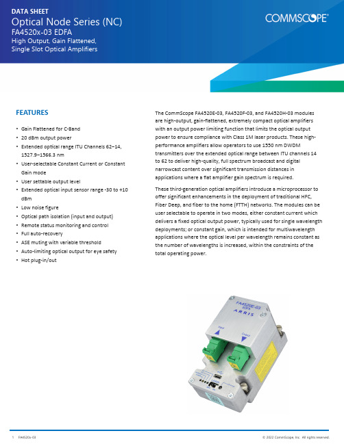
DATA SHEET Optical Node Series (NC)FA4520x-03 EDFA High Output, Gain Flattened, Single Slot Optical AmplifiersThe CommScope FA4520E ‐03, FA4520F ‐03, and FA4520H ‐03 modules are high ‐output, gain ‐flattened, extremely compact optical amplifiers with an output power limiting function that limits the optical output power to ensure compliance with Class 1M laser products. These high ‐performance amplifiers allow operators to use 1550 nm DWDM transmitters over the extended optical range between ITU channels 14 to 62 to deliver high ‐quality, full spectrum broadcast and digital narrowcast content over significant transmission distances in applications where a flat amplifier gain spectrum is required.These third ‐generation optical amplifiers introduce a microprocessor to offer significant enhancements in the deployment of traditional HFC, Fiber Deep, and fiber to the home (FTTH) networks. The modules can be user selectable to operate in two modes, either constant current which delivers a fixed optical output power, typically used for single wavelength deployments; or constant gain, which is intended for multiwavelength applications where the optical level per wavelength remains constant as the number of wavelengths is increased, within the constraints of the total operating power.•Gain Flattened for C ‐Band•20 dBm output power•Extended op cal range ITU Channels 62−14,1527.9−1566.3 nm•User ‐selectable Constant Current or ConstantGain mode•User settable output level•Extended optical input sensor range ‐30 to +10dBm•Low noise figure•Optical path isolation (input and output)•Remote status monitoring and control•Full auto ‐recovery•ASE muting with variable threshold•Auto ‐limiting optical output for eye safety•Hot plug ‐in/out FEATURESThis latest model offers extended amplification of optical input range down to ‐26 dBm per wavelength* to better support low level data signals. Input sensor range is extended down to ‐30 dBm. The automatic ASE muting has user settable thresholds where the EDFA output is muted when the incoming optical signal is below the threshold value with optical power automatically restored when the signal returns.*See detailed specifications regarding minimum input power and OSNR.Operational monitoring has been increased. This includes remote monitoring of optical levels, laser operating conditions, and alarm status with the option to set alarm parameters to suit local operating conditions.The units are designed as plug‐in modules for CommScope’s NC4000™series Fiber Node Platforms, including the NH4000 “Virtual Hub” and Universal Virtual Hub (UVHub), and, when used in the latter, provides a practical alternative to OTN‐style cabinets.SPECIFICATIONSPhysicalDimensions 4.0” L x 2.2” H x 2.3” W (10.2 cm x 5.6 cm x 5.8 cm)Weight0.6 lbs(0.3 kg)EnvironmentalOperating Temperature Range‐40°to +85°C (‐40°to 185°F)Storage Temperature Range‐40°to +85°C (‐40°to 185°F)Humidity5% to 95% non‐condensingGeneralHot plug‐in/outModes of Operation Constant Current or Constant GainASE Muting User enable/disable. When enabled, settable levels from ‐29 dBm to 10 dBm; power level for recovery is +1 dB fromset level.Optical InterfaceOptical Connectors SC/APCPower RequirementsInput Voltage24 V DCPower Consumption10 WStatus Indicator LEDs (5)CC (Constant Current Mode) LED On/Green = operating in constant current (power) modeCG (Constant Gain Mode) LED On/Green = operating in constant gain modeWarning LED On/Yellow = when•At least one Major Alarm has occurred•At least one Minor Alarm has occurred (Summary of Minor Alarms)•Any Alarm History is availableAlarm LED Major Alarm(s)On/Red = when at least one Major Alarm has occurred (Yellow Warning LED will also be on)NOTE: Available module status alarm options are viewed and managed in Opti‐Trace®CMS. Alarm severity (Major orMinor) for each parameter and threshold (alarm) minimum/maximum levels for Major and Minor alarms can bemanually set in Opti‐Trace CMS. Status indicator LEDs (Warning, Alarm, Status) are activated when a set threshold isexceeded.Status LED Red = laser switched offGreen = laser switched onOpticalInput Signal Wavelength1527.9−1566.3 nm (ITU 62−14)Optical Signal Path Isolation< ‐30 dBGain Flatness (Peak to Valley) 2.5 dB for 1527.9 to 1564.7 nm (ITU 62−16)4.5 dB for 1527.9 to 1566.3 nm (ITU 62−14)Constant Gain Mode (Preferred Operation Mode)The gain range is user settable from 6 to 30 dB.Full gain range may not be accessible depending upon input andoperating conditions. Gain ranges and composite input power ranges for the specified gain flatness are as follows:FA4520E FA4520F FA4520HGain Range1,216 to 20 dB12 to 16 dB8 to 12 dBInput Power Range‐10 to 4 dBm‐10 to 8 dBm‐10 to 12 dBmConstant Current ModeComposite Input Power Ranges for Specified Gain Flatness0 to 4 dBm4 to 8 dBm8 to 12 dBmNominal Output Power of 20 dBm Under Constant CurrentMode at Mid‐point Input Power Range2 dBm6 dBm10 dBmOutput Power Stability Constant Gain Mode ±0.7 dBConstant Current Mode: ±0.6 dBOutput Power Margin0.1 dB min; 0.4 dB maxOutput Power Min2 dBm. Automatically ensured by the module to prevent pump laser power from being near its threshold. This is toavoid pump laser fluctuation. Output power is kept 2 dBm or above regardless input power, constant gain or constantcurrent mode.Noise Figure Within the Above Specified Constant Gain and Constant Current Modes FA4520E: 5.0 dB typical, 5.5 dB max FA4520F: 5.5 dB typical, 6.0 dB max FA4520H: 6.0 dB typical, 6.5 dB maxInput Power for OSNR of 25 dB ‐26 dBm per wavelength (λ) with one EDFA (FA4521V) in system. With N units of FA4521V in the link, the requiredinput power for 25 dB OSNR is ‐26 dBm/λ + 10 log10(N). OSNR is defined as the ratio of signal power per wavelength tonoise power in 0.1 nm bandwidth at the output of the EDFA.Remote Monitoring/Control ParametersStatus Displayed Optical input and output power, EDFA gain, board temperature, ASE muting status, laser status, local summary.Local parameters for monitoring are displayed through USB port access.Control Parameter Constant gain and gain value; constant current mode and output power; ASE muting enable and thresholdNOTE:1.Gain can be set at 0.25 dB per step.2.When the actual EDFA gain (output power –input power) of a model falls within the respective range, specified gain flatness can be expected. Actual EDFA gain may be different fromset gain due to the limits of max output power (20 dBm) and minimum output power (2 dBm).ORDERING INFORMATIONFA4520E‐03‐AS Gain flattened EDFA, Single 20 dBm Output with variable level, ASE Muting & Power Limiting,Optimized for 18 dB Gain, Input power 0 to 4 dBm, Single slot module, SC/APC connectorsFA4520F‐03‐AS Gain flattened EDFA, Single 20 dBm Output with variable level, ASE Muting & Power Limiting,Optimized for 14 dB Gain, Input power 4 to 8 dBm, Single slot module, SC/APC connectorsFA4520H‐03‐AS Gain flattened EDFA, Single 20 dBm Output with variable level, ASE Muting & Power Limiting,Optimized for 10 dB Gain, Input power 8 to 12 dBm, Single slot module, SC/APC connectorsRELATED PRODUCTSNC4000 Optical Nodes NH/VH4000 VHub, UVHubOptical Patch Cords Optical PassivesFiber Service Cable Installation ServicesContact Customer Care for product information and sales:•United States: 866‐36‐ARRIS•International: +1‐678‐473‐5656Note: Specifications are subject to change without notice.Copyright Statement:©2022CommScope,Inc.All rights reserved.ARRIS,the ARRIS logo,NC4000,and Opti‐Trace are trademarks of CommScope,Inc.and/or its affiliates.All other trademarks are the property of their respective owners.No part of this content may be reproduced in any form or by any means or used to make any derivative work(such as translation,transformation,or adaptation)without written permission from CommScope,Inc and/or its affiliates(“CommScope”).CommScope reserves the right to revise or change this content from time to time without obligation on the part of CommScope to provide notification of such revision or change.。
TL-AP452C-PoE V1.0、TL-AP302C-PoE V1.0用户手册1.0.0

AP提供1个10M/100M自适应RJ45接口,用于连接IEEE 802.3af/at标准PoE供电设备。
-3-
无线吸顶式 AP
第2章 工作模式
AP支持两种工作模式:FAT AP模式和FIT AP模式。 当用户需要组建的无线网络规模较小时,可以使用FAT AP模式。此模式下,AP支持Web界面 管理,用户可以登录AP的Web管理界面进行无线功能设置,管理网络中的无线客户端,设置 AP的网络参数等。 当用户需要组建的无线网络规模较大时,若单独管理网络中的每一个AP,将使得网络管理工 作繁琐且复杂。此时,推荐用户在网络中搭建一台TP-LINK无线控制器产品,由无线控制器 统一管理网络中的所有AP。此情况下,AP只需工作在FIT AP模式即可。
此开关用于切换AP工作模式。切换模式后,AP将自动重启。 当开关拨到FAT时,表示AP工作在FAT AP模式。此模式适用于AP数量较少的网络环境,此模 式下,AP支持Web界面管理,可以登录Web界面对AP进行单独管理。FAT AP模式Web界面 管理方法,请参考2.1 FAT AP模式。 当开关拨到FIT时,表示AP工作在FIT AP模式。此模式适用于AP数量较多的网络环境,由AP 组建的局域网中需要接入TP-LINK无线控制器,可以登录无线控制器管理界面对本产品进行 功能配置。无线控制器的使用方法,请参考对应机型的说明书。 RJ45 接口
1.3.1 1.3.2
上盖 ......................................................................................................... 2 侧面板 ...................................................................................................... 2
博朗耳温计 IRT4520 英文原版说明书

How does Braun ThermoScan work?
Braun ThermoScan measures the infrared heat generated by the eardrum and surrounding tissues. To help to avoid inaccurate temperature measurements, the probe tip is warmed to a temperature close to that of the human body. When the Braun ThermoScan is placed in the ear, it continuously monitors the infrared energy. The measurement is finished and the result displayed when the thermometer detects that an accurate temperature measurement has been taken.
there is a risk of cross-contamination.
1. Guyton A C, Textbook of medical physiology, W.B. Saunders, Philadelphia, 1996, p 919 2. Guyton A C, Textbook of medical physiology, W.B. Saunders, Philadelphia, 1996, p 754-5 3. Netter H F, Atlas of Human Anatomy, Novartis Medical Education, East Hanover, NJ, 1997,
CH452中文手册
● 内置时钟振荡电路,不需要外部提供时钟或者外接振荡元器件,更抗干扰。 ● 支持低功耗睡眠,节约电能,可以被按键唤醒或者被命令操作唤醒。 ● 可选两种封装:SOP28、DIP24S,引脚与 CH451 芯片兼容。 ● 经过授权采用了 1 项专利技术,低成本,简便易用。
3、封装
4 线串行接口
输出
输入
输出 输出 输入
引脚说明
正电源,持续电流不小于 120mA 公共接地,持续电流不小于 120mA 数码管的段驱动,高电平有效, 键盘扫描输入,高电平有效,内置下拉 数码管的字驱动,低电平有效,
键盘扫描输出,高电平有效 串行接口方式选择,内置上拉电阻, 高电平选 4 线接口,低电平选 2 线接口
CH452 中文手册(一)
1
数码管驱动及键盘控制芯片 CH452
中文手册 版本: 1
1、概述
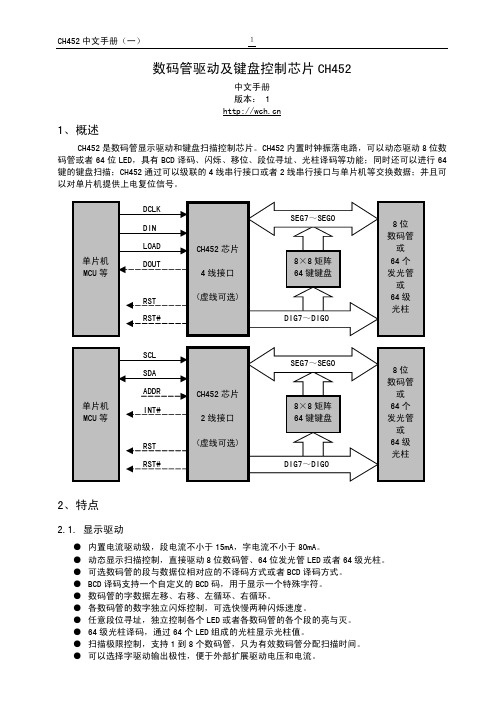
CH452 是数码管显示驱动和键盘扫描控制芯片。CH452 内置时钟振荡电路,可以动态驱动 8 位数 码管或者 64 位 LED,具有 BCD 译码、闪烁、移位、段位寻址、光柱译码等功能;同时还可以进行 64 键的键盘扫描;CH452 通过可以级联的 4 线串行接口或者 2 线串行接口与单片机等交换数据;并且可 以对单片机提供上电复位信号。
2.3. 外部接口
● 同一芯片,可选高速的 4 线串行接口或者经济的 2 线串行接口。 ● 4 线串行接口:支持多个芯片级联,时钟速度从 0 到 2MHz,兼容 CH451 芯片。 ● 4 线串行接口:DIN 和 DCLK 信号线可以与其它接口电路共用,节约引脚。 ● 2 线串行接口:支持两个 CH452 芯片并联(由 ADDR 引脚电平设定各自地址)。 ● 2 线串行接口:时钟速度从 500Hz 到 200KHz,兼容两线 I2C 总线,节约引脚。 ● 内置上电复位,可以为单片机提供高电平有效和低电平有效复位输出。
ADAM-4520使用说明
• ADAM-4520/4522快速入门手册(2010-06-07 02:02)关键字:分类:技术分享一、ADAM-4520/4522概述ADAM-4520/4522是有源的RS-232到RS-422/485的转换器,无须任何软件驱动,硬件配置正确即可实现转换功能。
RS-485端带有硬件自动数据流控制(自动流控,Automatic data flow),使用时无须额外进行软件自动流控;隔离保护,这样就有效的防止模块在收到高压冲击时而损坏。
信号端具有3000VDCADAM-4520/4522外观与ADAM-4000系列数据采集模块完全相同,安装方式有导轨安装、壁挂安装等,也可以与ADAM-4000数据采集模块叠加在一起。
波特率最高可以达到115.2kbps,使用10V-30V直流电源供电。
出厂默认设置:二、常规使用方法图1 ADAM-45204522连接示意图通过使用ADAM-4520,可以将主机(或PLC)上的RS-232串口转换为RS-422/485串口,从而实现连接更多设备、延长通讯距离等功能。
注意:当一对一通讯的时候,也可以反向使用,即将RS-485串口转换为RS-232串口,但是需要注意的是,ADAM-4520/4522无法设置RS-485设备的地址,因此反向使用时仅能用于一对一通讯!三、ADAM-4520/4522使用前必读1. ADAM-4520/4522连接一般PC机时,RS-232端应该使用串口直连线。
由图1可知,一般PC机的DB-9针串口,管脚2为Rx,管脚3为Tx;而4520的管脚2为Tx,管脚3为Rx;根据RS-232需要交叉Rx与Tx的要求,一般PC机与4520连接时使用串口直连线即可。
2. 使用RS-485/422通讯时,需要设置数据格式。
SW1用来设置数据格式,可以是9、10、11、12位(bits)。
默认的数据格式是10bits:1起始位,8数据位,0校验位,1停止位。
TEC b-452HS 用户使用说明
1.2 附件--------------------------------------------------------------------------------------1
2. 规格-----------------------------------------------------------------------------------------------2
6.2 安装供纸架顶盖--------------------------------------------------------------------- 7
6.3 连接电源线和电缆-------------------------------------------------------------------8
警告
下面的指示表示如果对机器进行不合适的与指示相反的操作时, 可能有引起死亡或严重伤害的危险.
禁止接入任何与规定交流 电压不符的电源.
■不要使用与标牌上指定 的交流电压不同的电源, 这可能导致火灾或电击
禁止
■不要用潮湿的手拔插 电源插头, 这可能引起 电击
禁止 禁止
■如果本机器和另外耗 电较大的设备公用同一 个电源插口, 每当这个 设备工作时电压可能有 很大波动. 一定要为本 机器提供专用插口, 否 则会引起故障.
2.1 一般规格--------------------------------------------------------------------------------2
2.2 打印机规格---------------------------------------------------------------------------- 2
ADAM4520转换模块分析报告
附录:ADAM-4520 模块原理图
图一 模块供电原理图 图二 信号处理原理图
择 选 式 方 讯 通 或 特 波 讯 通 择 选 式 格 据 数 置 设 阻 排 振 晶 源 有 ? ?? ? 管 极 二 制 抑 态 瞬
RS485 转换过程中自动数据流控制主要依靠检测 RS232 端的 RTS CTS 两个信号电平变化 来实现。RTS 是请求发送信号;CTS 为清除发送信号;即对 PC 端来说当 CTS 为低电平停止 发送数据,为高电平时恢复发送数据;当 PC 端正可以接收数据时,RTS 为高电平;正在 接收数据 RTS 为低电平。
模 式 : 4 线 RS-422 , 4 线 RS-485 , 2 线 RS-485( 通 过 拨 码 开 关 选 择 ) RS-485 数据流向控制:自动 光电隔离:3000V
4、 机械特性
外形尺寸(长*宽*高):60*120*25,具体安装尺寸可见使用说明书。
5、 模块原理框图
图 5.1 模块系统框图
8.1 系统供电原理分析
首先采用了电源芯片 7D26 将输入+10V 到+30V 的电压转化为+5V1 为 CPLD XC9536 与双 向收发控制芯片 75LBC176 以及高速光隔 H11L1 422/485 信号侧供电。7D26 几乎查阅不到 相关的技术资料,从原理上分析应该是输入电压为+10V 到+30V 输出电压为+5V 的非隔离 式的稳压电源芯片,从整个模块功耗来看 7D26 的功率应该在 1.5W-2W 之间。
在 RS232/RS485 过程中,U3 发送驱动器与接收驱动器由 CPLD 控制使能端交替工作, 完成 RS485 的半双工通信。其中自动数据流控制原理随后说明。
4520模块中文操作手册

3.2 端口说明.................................................................................................................... 9
3.3 电源要求.................................................................................................................... 9
3.8 通讯端口.................................................................................................................. 15
3.9 通讯端口用法........................................................................................................... 15
本出版物设计到符号释义本出版物设计到符号释义本出版物设计到符号释义本出版物设计到符号释义
DEEP SEA ELECTRONICS PLC
DSE4510 / DSE4520 操作手册
文件编号: 057-171
作者: Allan Jones
DSE4510/DSE4520 操作手册
DSE4510/4520 操作手册
DSE商标以及名称是Deep Sea Electronics公司在英国注册的。
本出版物内所有带有注册商标标志的产品名称归各自公司所有。
Deep Sea Electronics公司保留对本文档进行修订的权利,若有改动,恕不另行通知。
亚当模块4520说明书

ADAM-4520/4522快速入门手册一、ADAM-4520/4522概述ADAM-4520/4522是有源的RS-232到RS-422/485的转换器,无须任何软件驱动,硬件配置正确即可实现转换功能。
RS-485端带有硬件自动数据流控制(自动流控,Automatic data flow),使用时无须额外进行软件自动流控;隔离保护,这样就有效的防止模块在收到高压冲击时而损坏。
信号端具有3000VDCADAM-4520/4522外观与ADAM-4000系列数据采集模块完全相同,安装方式有导轨安装、壁挂安装等,也可以与ADAM-4000数据采集模块叠加在一起。
波特率最高可以达到115.2kbps,使用10V-30V直流电源供电。
出厂默认设置:二、常规使用方法图1 ADAM-45204522连接示意图通过使用ADAM-4520,可以将主机(或PLC)上的RS-232串口转换为RS-422/485串口,从而实现连接更多设备、延长通讯距离等功能。
注意:当一对一通讯的时候,也可以反向使用,即将RS-485串口转换为RS-232串口,但是需要注意的是,ADAM-4520/4522无法设置RS-485设备的地址,因此反向使用时仅能用于一对一通讯!三、ADAM-4520/4522使用前必读1. ADAM-4520/4522连接一般PC机时,RS-232端应该使用串口直连线。
由图1可知,一般PC机的DB-9针串口,管脚2为Rx,管脚3为Tx;而4520的管脚2为Tx,管脚3为Rx;根据RS-232需要交叉Rx与Tx的要求,一般PC机与4520连接时使用串口直连线即可。
2. 使用RS-485/422通讯时,需要设置数据格式。
SW1用来设置数据格式,可以是9、10、11、12位(bits)。
默认的数据格式是10bits:1起始位,8数据位,0校验位,1停止位。
当使用ADAM-4000模块时,默认设置即可通讯。
当使用其它厂家产品时,如果通讯参数不是“N,8,1”,则需要根据通讯参数来设置SW1。
海康威视4520添加报警主机操作手册

4520 HIDDNS 方式添加报警主机操作手册目录一、操作流程(配置流程) (1)二、操作步骤(配置步骤) (1)三、适用型号 (5)四、变更记录 (5)五、关于海康威视 (1)一、操作流程(配置流程)1.设备注册HIDDNS;2.4520 添加报警主机3.验证是否成功接入二、操作步骤(配置步骤)1.设备注册HIDDNS;(1)在路由器页面进行端口80、800、554 端口映射,映射界面见下图:映射完成后查看是否成功;(2)在4200 中进行HIDDNS 注册:高级功能中设置dns 地址,dns 地址可从路由器中查看:在4200 远程配置中网络-----DDNS 中勾选启用DDNS,服务协议选择HIDDNS;输入设备域名,完成注册2.4520 添加设备在4520 中点击菜单选项,进入”设备管理”,点击右上方添加,输入相关信息:完成添加.3.验证是否成功接入首先开启4520 中的推送设置:对报警主机进行控制、触发观察手机是否收到推送消息三、适用型号四、五、关于海康威视海康威视是以视频为核心的物联网解决方案提供商,面向全球提供综合安防、智慧业务与大数据服务。
海康威视全球员工超26000人(截止2017年底),其中研发人员和技术服务人员超13000人,研发投入占企业销售额的7-8%,绝对数额占据业内前茅。
海康威视是博士后科研工作站单位,以杭州为中心,建立辐射北京、上海、重庆、武汉以及加拿大蒙特利尔、英国利物浦的研发中心体系,并计划在西安、武汉、成都、重庆和石家庄建立新的研发基地。
海康威视拥有视音频编解码、视频图像处理、视音频数据存储等核心技术,及云计算、大数据、深度学习等前瞻技术,针对公安、交通、司法、文教卫、金融、能源和智能楼宇等众多行业提供专业的细分产品、IVM智能可视化管理解决方案和大数据服务。
在视频监控行业之外,海康威视基于视频技术,将业务延伸到智能家居、工业自动化和汽车电子等行业,为持续发展打开新的空间。
基本型扭矩传感器4520A说明书

Instruction Manual Basic Line Torque SensorType 4520A...äInstructionManual Basic Line Torque SensorType 4520A...äForewordForewordThis manual applies to the Basic Line Torque Sensor Type4520A… .The instruction manual must be kept on hand for futureuse, and must be available at the site of implementation ofthe NC joining system, as needed.The specifications in this manual can change at any timewithout prior notification. Kistler reserves the right to im-prove and to change the product for the purpose of tech-nical progress without the obligation to inform persons andorganizations as the result of such changes.Original language of these operating instructions: German© 2009 … 2014 Kistler Group. All rights reserved.Kistler GroupEulachstrasse 228408 WinterthurSwitzerlandPhone +41 52-224 11 11Fax +41 52-224 14 14****************Product CenterTorque Sensors, NC Joining Systems,Force-Displacement Monitoring, Test Stand SystemsKistler Lorch GmbHMaierhofstrasse 3573547 LorchGermanyPhone +49 7172-184 0Fax +49 7172-184 400********************Basic Line Torque Sensor Type 4520A... Content1.Introduction (3)2.Important Information (4)2.1Disposal Instructions for Electrical and Electronic Equipment (4)3.Application and Key Features (5)4.Description of the Measuring System (6)4.1Mechanical Design (6)4.2Electrical Block Diagram (7)4.2.1Examples of Application (8)4.3Electrical Configuration of Speed Measurement (9)5.Electrical Connections of the Sensor (10)5.1Plug Connection (11)5.1.1Installing the Signal Lead (11)5.2Instruction for Electrical Installation (12)5.3Connection Cables (13)5.4Mechanical Installation of the Torque Sensor (14)5.5Possible Installation Type 4520A... . (15)6.Mechanical Application and Mechanical Istallation of the Torque Sensor Type 4520A... (16)6.1Frictional Torque Control in Production (16)6.2Torque Measuring Shaft Version RA (17)6.3Supply and Evaluation (18)7.Static Calibration (19)7.1Construction of a Simple Calibration Device (19)7.2Calculation Example for Lever Arm Length (20)8.Maintenance (21)9.Repairs (22)10.Declaration of Conformity (23)11.Accessories and Ordering Key (24)12.Index (25)Total Pages 25Introduction1.IntroductionPlease take the time to thoroughly read this instructionmanual. It will help you with the installation, maintenance,and use of this product.To the extent permitted by law Kistler does not accept anyliability if this instruction manual is not followed or prod-ucts other than those listed under Accessories are used.Kistler offers a wide range of products for use in measuringtechnology:▪Piezoelectric sensors for measuring force, torque, strain,pressure, acceleration, shock, vibration and acoustic-emission▪Strain gage sensor systems for measuring force and torque▪Piezoresistive pressure sensors and transmitters▪Signal conditioners, indicators and calibrators▪Electronic control and monitoring systems as well as soft-ware for specific measurement applications▪Data transmission modules (telemetry)▪E lectromechanical NC joining modules and force-displacement monitors▪Test bed systems for electric motors and gear units for la-boratory, manufacturing, and quality assuranceKistler also develops and produces measuring solutions forthe application fields engines, vehicles, manufacturing,plastics and biomechanics sectors.Our product and application brochures will provide youwith an overview of our product range. Detailed datasheets are available for almost all products.If you need additional help beyond what can be found ei-ther online or in this manual, please contact Kistler's exten-sive support organization.Basic Line Torque Sensor Type 4520A...2. Important Information2.1Disposal Instructions for Electrical and Electronic EquipmentDo not discard old electronic instruments in municipal trash. For disposal at end of life, please return this product to an authorized local electronic waste disposal service or contact the nearest Kistler Instrument sales office for return instructions.Application and Key Features3.Application and Key Features▪Measuring ranges from 1 ... 1 000 N·m▪Speed up to 10 000 min-1▪Torque meter with strain gages measuring system▪Wear-resistant transmission of the measuring signal, inte-grated amplifier▪Measurement of constant and variable torques▪Torque measurement on the rotating shaft▪Integrated speed measurement▪Application in the laboratory, manufacture and qualitycontrol▪Great value for moneyFig. 1: Basic Line torque sensor Type 4520A...Basic Line Torque Sensor Type 4520A...4.Description of the Measuring System4.1Mechanical DesignBasic Line torque sensors Type 4520A… consist of a base body which contains the measuring shaft. On the mea-suring shaft there is a torsional section with strain gages and electronics with signal amplifier and A/D transformer. The connection box of the base body contains the statio-nary electronics for the signal formation.The base body of the sensor offers different assembly posi-tions.Fig. 2: Mechanical design Basic Line torque sensor Type 4520A...External electronic Cable connectorShaftBearingSensorStrain gageBearingSpeed measuring systemRotating electronicsDescription of the Measuring System4.2Electrical Block DiagramFig. 3: Electrical block diagramBasic Line Torque Sensor Type 4520A...4.2.1Examples of ApplicationStrict use of electrical isolation for feed and measuring sig-nal.Fig. 4: Separate speed and measuring supplyShared access measuring supply for feed and measuring supply.Interlink the power and measuring supply, evaluation electronic is to be made.Fig. 5: Power and measuring supply in the evaluation electronic combinedDescription of the Measuring System4.3Electrical Configuration of Speed MeasurementSpeed measurement is effected photo-electrically byevaluating the light, which shines through a grid wheel.A gallium-arsenide light diode serves as transmitteremitting in the near infrared. In a phototransistor thelight is converted into an electric signal and after apulse shaper made available as "open collector" signal.The input current amounts max. 16 mA.Fig. 6: Electrical block diagram of speed measurementFig. 7: Electrical CMOS- or TTL input circuit/opticallyisolated input circuitBEExternal counter withhigh imput impendanceBEBE0 VExternalcounterBasic Line Torque Sensor Type 4520A...5. Electrical Connections of the SensorFig. 8:Electrical connectionsShielded lead of 0,14 mm² nominal cross sectionShielded leadLead connectorTo power supply unit and displayTorque sensor Type 4520A…Electrical Connections of the Sensor5.1Plug ConnectionPin Allocation of Built-in 12 pin ConnectorFunction Pin DescripptionPower Supply F +U B18 ... 26 VDC, power consumption <2 WE GND Reference for U B and angle signalsShield M In sensor; connected to caseTorque output C U A±10 VDC at M nom at >2 kΩ10 VDC at control signal revolutionR i.C = 10 Ω, output with short-circuit protec-tion connection to AGNDD AGND Reference for U ASpeed sensor B Track A Open collector outputInternal 1 kΩ resistance to 5 VDC (pull up),TTL-levelInput K Control Off: 0 ... 2 VDC100 % control input On: 5 ... 30 VDCA KGND Reference for controlG ReservedH ReservedJ ReservedL Reserved5.1.1Installing the Signal Lead▪Do not run the lead parallel to power cables or control cir-cuits.▪Do not place the lead close to equipment producingstrong electromagnetic fields, e.g. transformers, welders,contactors, electric motors, etc.▪If such situations cannot be avoided, run the lead insideearthed steel conduit.▪Make a loop in the lead when fixing it at the torque sensorso that it is not damaged by vibration.▪If supply and evaluation unit are galvanically connected, adifferential input must be used for the torque singal toprevent that the voltage drop on the 0 V-supply line af-fects the measured signal.Basic Line Torque Sensor Type 4520A...5.2 Instruction for Electrical InstallationFig. 9: Electrical installation▪ Please ensure correct functioning of the shield for the connection cable!▪ To improve the electrical contact area between stator housing base and machine base, it's recommended to remove the anodization of the bottom of the stator housing.Electrical Connections of the Sensor5.3Connection CablesBasic Line Torque Sensor Type 4520A...5.4Mechanical Installation of the Torque SensorThere are different methods of installing the torque sensor,depending on the application.Since very high lateral forces and bending moments mayoccur even at small axial displacement, the torque sensormust always be mounted with couplings.Generally▪The plant must be secured with a burst protection corre-sponding to the machine protection law.▪We recommend calculating the shafting according to thetorsion- and bending critical speeds. These speeds shouldbe avoided during operation. For a safe operation of theunit we recommend to remain approx. 30 % below orabove the critical speeds.▪After installation depending on speed the unit should bebalanced according to DIN 2060.▪The machine vibrations should be checked according toVDI 2056.LiteratureDubbel pocket book for machine engineering, published bySpringer.F. Holzweißig, H. Dresig, textbook of machine dynamics,published by Springer.DIN 2056 evaluation rules for mechanic vibrations of ma-chines.Electrical Connections of the Sensor5.5 Possible Installation Type 4520A...Torque sensor between drive and brakeFig. 10:Together with the half couplings the torque sensor forms a full couplingCouplings compensate for axial-radial and angular mis-alignment.The connection of shaft and coupling hub is positively locked by a clamping element.The torque measuring shaft is only a part of the power train. Radial and torsional vibrations may have a very bad impact on the performance of the torque shaft and the measuring signal.For that reason the operating speed must not be near the critical speed, either it has to be far underneath or above it.BrakeHalf couplings Type 2302A... Drive (specimen) Twist protection (should not apply heavy tension-forces on the torque sensor)Torque sensorBasic Line Torque Sensor Type 4520A...6. Mechanical Application and Mechanical Installation of the Torque Sensor Type 4520A...6.1Frictional Torque Control in ProductionFig. 11: Application example Type 4520A...EngineTorsion proof miniature coupling double-flexible with clamping hubType 2303A...Basic Line Torque Sensor rotating with contactfree signal transmissionType 4520A...Torsion proof miniature coupling double-flexible with clamping hubType 2303A...Bearing mounting Test specimen fixture spring-loaded actuatorAngle supportMechanical Application and Mechanical Installation of the Torque Sensor Type 4520A...6.2 Torque Measuring Shaft Version RAFor the electric connection of measuring shaft and supply- and evaluation unit we recommend to use the shielded signal lead, Type KSM072030-5 (Mat. No.: 18008943) with low capacity.As supply and evaluation unit we suggest the Control Monitor CoMo Torque Type 4700B... .The matching connection cable is Type KSM018538-2,5 (Mat. No.: 18008963).As an alternative solution the units Type 4704A…, model VA3600 without display can be used.Assembly set Type KSM035681 (Mat. No.: 18024830) as accessories for VA3600 for the connection of the torque measuring shaft Type 4520A… .The signal lead should not exceed a length of 30 meters. Do not run the lead parallel to power cables or control cir-cuits.The pin connection is explained in chapter "Plug Connec-tion" of this manual.On each side of the torque measuring shaft there is a high quality bearing installed. The installation can have any po-sition, however offset couplings must always be applied to balance geometrical errors and keep false loads away from the torque measuring shaft.Radial, axial, diagonal and angular errors are compensa-ted by:▪ Multi-disk couplings, e.g. Type 2303A... ▪ Membran ▪ Claw couplingsType 4500B…Type 4704A…Basic Line Torque Sensor Type 4520A...6.3 Supply and EvaluationThe sensor may only be operated using filtered 24 VDC voltage.Recommended supply voltage:Fig. 12: Supply circuit and evaluationType 4704A... VA3600Type 4520A… (Data sheet 000-934)L1 PE N~=0 V +18 ... 26 V Torque output ±10 VDC Panel meter Quadrature counter PLCPC, processing of measuring data Speed output 1 5 V, TTLTerminal box for Type 4520A… 0 V (Data sheet 000-765)Static Calibration7. Static CalibrationThis procedure requires the use of a calibration device with a lever arm and weights for producing specific values of torque.The calibration procedure is as follows▪ Apply the rated value of torque to the torque meter and then remove it again▪ Adjust the zero reading accurately▪ Apply a known value of torque to the torque meter ▪ Adjust the displayed reading to the corresponding valuePlotting a calibration curve▪ Calibrate the torque meter as described above▪ Apply torque in 1/10 steps up to the full rated value and then remove it again in the same way.▪ A delay of at least 30 seconds must be allowed between the individual 1/10 steps so that each reading can stabilize before it is recorded.7.1 Construction of a Simple Calibration DeviceFig. 13: Calibration deviceK KTorque sensorType 4520A… Lever arm Lever armK = loose half-couplings Counter bearing Lever arm bearing (duplex) Weight (calibrated)Lever arm- bearingBasic Line Torque Sensor Type 4520A...7.2 Calculation Example for Lever Arm Lengthgm ML ⋅=, whereby M = TorqueL = Length of lever arm required m = Mass required g = 9.80665 m/s²(= standard gravity – varies with location)Fig. 14:Calculation of lever arm lengthExample: m = 1 kg Mt = 10 N·m10 N·m s 2 L = = 1,0197 m 1 kg x 9,80665 mMaintenance8.Maintenance▪Sensors of the Type 4520A… are almost maintenance-free.▪Durability of bearings in rated temperature range is ap-prox. 20 000 hours.▪Durability of bearings in working temperature range is ap-prox. 10 000 hours.▪Renewal of bearings can only be effected at works.▪Precision applications: Yearly calibration of sensor (calibra-tion at works or with adequate calibration device).▪Control correct cable plug position monthly.▪Check cables for damages monthly.▪Annual re-calibration of torsional momentBasic Line Torque Sensor Type 4520A...9.RepairsFault Cause RemedyShaft stiff to turn Bearing defect due toa) torsional or flexural vibrationb) high axial or radial loadsc) worn bearingsd) bent shaftReturn to factoryZero shift less than 2 % Torsional vibrationTorsional shockThe zero reading canbe readjusted at thedisplay.Zero shift between approx. 2 and 5 % of full scale Sensor overloadedTorsional vibrationPuch momentsThe zero reading can bereadjusted once at thedisplay.Hysteresis between clockwise and anticlockwise torque Sensor overload through highdynamic load or torsional vibra-tion.Return to factoryDeclaration of Conformity10.Declaration of ConformityBasic Line Torque Sensor Type 4520A...Measuring Range in N·m1001 2002 5005 10010 20020 5005010010020020050050010001k0Ordering Example Type4520A010Torque sensor: Rated to rque 10 N·m:010Ordering KeyIncluded Accessories•NoneOptional Accessories Type/Art. No.•Female cable connector KSM000703with solder lug12 pin•Connecting cable, length 5 m, 12 pin KSM124970-5– flying leads•Connecting cable, length 2,5 m, 12 pin KSM185380-2,5– CoMo Torque•Control Monitor CoMo Torque4700B...evaluation instrument for torque sensors(see data sheet 4503A_000-595)•Connecting cable, length 5 m KSM07203-512 pin neg. – 12 pin pos.11.Accessories and Ordering KeyIndex12.IndexAAccessories and Ordering Key (24)Application/Key Feautures (5)Applikationsbeispiele (8)CCalculation Example for Lever Arm Length 20 Construction Calibration Device (19)DDeclaration of Conformity (23)Description of the Measuring System (6)Disposal Instructions (4)EElectrical Block Diagram (6)Electrical Configuration of Speed Measurement 9 Electrical Connections of the Sensor (10)Examples of Application (8)FFrictional Torque Control in Production (16)HHelp .......................................................... 3 IImportant Information (4)Installing the Signal Lead (11)Instruction for Electrical Installation (12)Introduction (3)MMaintenance (21)Mechanical Application and Mechanical Installation (16)Mechanical Design (6)Mechanical Installation (14)PPlug Connection (11)Possible Installation Type 4520A... (15)RRepairs (22)SStatic Calibration (19)Supply and Evaluation (18)TTorque Measuring Shaft Version RA (17)。
tr4520 使用说明书

tr4520 使用说明书
1、文档盖板:将文档放在稿台玻璃上时,打开此盖板。
2、操作面板:用于更改设置或操作本机。
3、LCD(液晶显示屏):显示信息、菜单选项和操作状态。
4、靠纸架:承托已装入托盘的纸张。
装载纸张前将其扩展。
要扩展靠纸架,将手指放入圆形的凹槽,然后将扩展架拉出,直至不能再拉出为止。
5、纸张导片:装载纸张时,请捏紧手柄并将纸张导片对齐纸张左侧边缘。
6、供纸器盖:打开此盖以在自动供纸器中装入纸张。
7、出纸托盘扩展架:承托输出的打印输出。
打印前将其扩展。
8、出纸托盘:打印的纸张输出至此。
在打印之前打开。
9、直接打印端口:用于从支持“PictBridge”的数码相机或数码摄像机进行直接打印。
10、将可选 Bluetooth 单元 BU-20 插入可以通过 Bluetooth 通讯进行无线打印。
11、IrDA 端口:通过红外通讯接收移动电话发送的照片数据。
12、存储卡插槽盖:将其打开插入存储卡。
13、后端托盘:可以轻松装载不同类型的纸张。
14、一次可以放置一页或多页纸张,并且纸张将每次自动送入一页。
15、靠纸架导片:将纸张右侧对齐此导片。
- 1、下载文档前请自行甄别文档内容的完整性,平台不提供额外的编辑、内容补充、找答案等附加服务。
- 2、"仅部分预览"的文档,不可在线预览部分如存在完整性等问题,可反馈申请退款(可完整预览的文档不适用该条件!)。
- 3、如文档侵犯您的权益,请联系客服反馈,我们会尽快为您处理(人工客服工作时间:9:00-18:30)。
3.5.3 电流互感器相位.................................................................................................... 12
3.5.4 电流互感器等级.................................................................................................... 12
3.4 发电机电压/频率检测.................................................................................................. 9
3.5 发电机电流检测........................................................................................................ 10
3.5.1 电流互感器 CT 变比..............................................................................................11
3.5.2 电流互感器极性.................................................................................................... 12
3.2 端口说明.................................................................................................................... 9
3.3 电源要求.................................................................................................................... 9
DEEP SEA ELECTRONICS PLC
DSE4510 / DSE4520 操作手册
文件编号: 057-171
作者: Allan Jones
DSE4510/DSE4520 操作手册
DSE4510/4520 操作手册
DEEP SEA ELECTRONICS PLC
Highfield House Hunmanby North Yorkshire YO14 0PH ENGLAND
3.6 输入......................................................................................................................... 13
3.6.1 数字输入............................................................................................................... 13
销售电话: +44 (0) 1723 890099 销售传真: +44 (0) 1723 893303
电子邮件 : sales@ 网站地址:
DSE4510/DSE4520 操作手册
© Deep Sea Electronics Plc 版权所有。 除《1988年版权、设计和专利法案》条款规定之外,如未获得版权所有者的书面许可,不得以任何 方式(包括影印、电子版形式存储在媒介中或者其它方式)复制本出版物的任何部分。
如需复制本出版物任何部分而向版权所有者申请书面许可,请将申请书寄至上述Deep Sea Electronics公 司地址。
DSE商标以及名称是Deep Sea Electronics公司在英国注册的。
本出版物内所有带有注册商标标志的产品名称归各自公司所有。
Deep Sea Electronics公司保留对本文档进行修订的权利,若有改动,恕不另行通知。
1.3 培训指南..................................................................................................................... 6
1.4 第三方文档.................................................................................................................. 6
2 引言..................................................................................................................................... 7
3 说明..................................................................................................................................... 8
1.1 安装说明..................................................................................................................... 6
1.2 手册............................................................................................................................ 6
3.6.2 模拟量输入........................................................................................................... 13
3.6.2.1 机油压力传感器................................................................................................ 13
3.1 产品编号.................................................................................................................... 8
3.1.1 简称....................................................................................................................... 8
2
DSE4510/4520 操作手册
目录
章节
页码
1 参考文献............................................................................................................................. 6
3.10 仪表累计................................................................................................................ 16
3.11 尺寸和安装............................................................................................................. 17
3.6.2.2 水温传感器....................................................................................................... 12
3.6.2.3 灵活传感器....................................................................................................... 13
3.9.1 CAN 通讯.............................................................................................................. 15
3.9.2 USB 连接..............................................................................................................16
3.7.1 输出 A&B............................................................................................................. 14
3.7.2 输出 C D E F.......................................................................................................... 14