数字隔离器(磁隔离)产品常见问题解答(ADI)
ADI ADuM6420A带DC/DC转换器的四道数字隔离器解决方案
ADI ADuM6420A带DC/DC转换器的四道数字隔离器解决方案ADI公司的ADuM6420A/ADuM6421A/ADuM6422A是采用isoPower®集成隔离式直流/直流转换器的四通道数字隔离器.基于ADI 公司的iCoupler®技术,可提供稳压隔离式电源,在配备铁氧体的2 层印刷电路板(PCB)上在满载时符合CISPR 32/EN 55032 B 级限制.100mA输出电流,满足AEC-Q100汽车应用规范, 在500 mW的隔离式设计中不再需要单独的隔离式直流/直流转换器.具有四路DC到100Mbps信号隔离通路,可提供外形小巧四个独立的完全隔离式解决方案.高温125C工作温度,共模瞬态免疫为100 kV/μs, VIORM = 566 V peak.主要用在RS-232 收发器,电源启动偏置和栅极驱动,隔离式传感器接口和工业可编程逻辑控制器(PLC)以及汽车车载充电器(OBC)和DC/DC转换器.本文介绍了ADuM6420A/ADuM6421A/ADuM6422A/ADuM6423A/ ADuM6424A主要特性,功能框图,.评估板EVAL-ADUM6421ARNZ/ EVAL-ADUM6421AURNZ主要特性,电路图,材料清单和PCB设计图.The ADuM6420A/ADuM6421A/ADuM6422A/ADuM6423A/ ADuM6424A1 are quad-channel digital isolators with an isoPower®, integrated, isolated dc-to-dc converter. Based on the Analog Devices, Inc., iCoupler® technology, the dc-to-dc converter provides regulated, isolated power that meets CISPR 32/EN 55032 Class B limits at a full load on a 2-layer printed circuit board (PCB) with ferrites. Popular voltage combinations and the associated output current levels are listed in Table 1.The ADuM6420A/ADuM6421A/ADuM6422A/ADuM6423A/ ADuM6424A eliminate the need for a separate, isolated dc-to-dc converter in 500 mW, isolated designs. The iCoupler chip scale transformer technology is used for isolated logic signals and for the magnetic components of the dc-to-dc converter. The result is a small form factor, total isolation solution.The ADuM6420A/ADuM6421A/ADuM6422A/ADuM6423A/ ADuM6424A isolators provide four independent isolation channels (see the Pin Configurations and Function Descriptions for additional information).ADuM6420A主要特性:isoPower integrated, isolated dc-to-dc converter100 mA output supplyAEC-Q100 qualified for automotive applicationsADuM6421AW (ADuM6423AW pending)Meets CISPR 32/EN55032 Class B emission limits up to 5 Mbps at a full load on a 2-layer PCBQuad dc to 100 Mbps signal isolation channels28-lead, fine pitch, SOIC with 8.3 mm minimum creepageHigh temperature operation: 125C maximumHigh common-mode transient immunity: 100 kV/μsSafety and regulatory approvals (pending)UL recognition (pending)5000 V rms for 1 minute per UL 1577CSA Component Acceptance Notice 5A (pending)VDE V 0884-11 certificate of conformity (pending)VIORM = 566 V peakCQC certification per GB4943.1-2011 (pending)ADuM6420A应用:RS-232 transceiversPower supply start-up bias and gate drivesIsolated sensor interfacesAutomotive on-board charger (OBC) and dc to dcIndustrial programmable logic controllers (PLCs)图1.ADuM6420A功能框图评估板EVAL-ADUM6421ARNZThe ADuM6420A/ADuM6421A/ADuM6422A/ADuM6423A/ ADuM6424A devices integrate fouriCoupler® on-off keying (OOK) digital isolation channels and iCoupler chip scale isoPower® transformer technology.This iCoupler transformer technology enables a small form factor integrated, reinforced isolated signal and power solution, in applications requiring up to 500 mW of isolated power.Available dc-to-dc converter supply configurations and maximum available power at the elevated ambient temperatures are specified in the ADuM6420A/ADuM6421A/ADuM6422A/ADuM6423A/ ADuM6424A data sheet.The ADuM6420A/ADuM6421A/ADuM6422A/ADuM6423A/ ADuM6424A devices provide regulated, isolated power that meets CISPR 32/EN 55032, Class B limits at full load on a 2-layer printed circuit board (PCB) with ferrite beads. Radiated emissions test plots of theEVAL-ADUM6421ARNZ/EVAL-ADUM6421AURNZ are provided in Figure 4 and Figure 5. All devices inthe family include the same isolated dc-to-dc converter and are differentiated by directional digital channel configurations.The EVAL-ADUM6421ARNZ includes the ADuM6421ABRNZ5 quad-channel digital isolator with integrated, isolated dc-to-dc converter. Alternatively, the EVAL-ADUM6421AURNZ leaves the isolator position unpopulated to support evaluation of the ADuM6420A, ADuM6421A, ADuM6422A, ADuM6423A, or ADuM6424A.Full specifications for the ADuM6420A/ADuM6421A/ ADuM6422A/ADuM6423A/ADuM6424A are available in the ADuM6420A/ADuM6421A/ADuM6422A/ADuM6423A/ ADuM6424A data sheet, which must be consulted in conjunction with this user guide when using the evaluation boards.评估板EVAL-ADUM6421ARNZ主要特性:isoPower integrated, isolated dc-to-dc converterMeets CISPR 32/EN 55032, Class B emission limitsOn-board 6 V to 9 V LDO power supply that provides 5 V to the VDDP pin5 V input operation and selectable 3.3 V or 5 V isolated dc-to-dc converter outputScrew terminal connectors for the followingLDO power supply5 V direct power supplyOff board PDIS controlIsolated output supplyEVALUATION KIT CONTENTSEVAL-ADUM6421ARNZ, includes the ADuM6421ABRNZ5EVAL-ADUM6421AURNZ, requires the ADuM6420A, ADuM6421A, ADuM6422A, ADuM6423A, or ADuM6424A to be ordered separately图2.评估板EVAL-ADUM6421ARNZ外形图图3.评估板EVAL-ADUM6421AURNZ外形图图4.评估板EVAL-ADUM6421ARNZ/EVAL-ADUM6421AURNZ电路图评估板EVAL-ADUM6421ARNZ/ EVAL-ADUM6421AURNZ材料清单:图5.评估板EVAL-ADUM6421ARNZ/ EVAL-ADUM6421AURNZ PCB设计图(顶层)图6.评估板EVAL-ADUM6421ARNZ/ EVAL-ADUM6421AURNZ PCB设计图(底层)。
数字隔离器的电源要求是什么

数字隔离器的电源要求是什么数字隔离器是一种电子器件,通常用于隔离电气回路,以确保高电压和低电压电路之间的安全分离。
数字隔离器需要电源来运行,并且在安装过程中有一些特定的电源要求,以确保其他电子设备的稳定性和安全性。
在本文中,我们将探讨数字隔离器的电源要求是什么。
输入电源数字隔离器需要一个输入电源来工作。
输入电源的电压范围取决于数字隔离器的型号和要求。
通常,数字隔离器都需要一个直流电源,输入电压的范围一般在5V至24V之间,可能稍高或稍低。
输入电源必须符合数字隔离器的电压范围要求,否则可能会导致数字隔离器无法正常工作。
在选择输入电源时,需要确保其能够稳定地提供所需的电压和电流。
电源功率数字隔离器需要一定的电源功率来工作。
如果电源功率不足,可能会导致数字隔离器无法正常工作或产生失真、噪声等问题。
因此,需要合理地选择具有足够电源功率的电源和电源类型。
噪声数字隔离器的输入电源必须是低噪声的。
高噪声电源会导致数字隔离器产生噪音和失真。
而低噪声电源则可以提高数字隔离器的精度和稳定性。
绝缘要求数字隔离器是为了隔离不同电气回路而设计的,因此,其输入和输出端之间需要有绝缘措施以防止互相干扰。
因此,输入电源必须经过隔离,并且数字隔离器自身还要具备高绝缘电压性能,以保证输入和输出之间的隔离效果。
滤波数字隔离器输入电源还需要滤波,以滤除电源中的高频噪声,以确保数字隔离器的精度和稳定性。
简单而低成本的滤波方法是使用电容、电感和电阻来构成RC滤波器。
结论因此,在选择数字隔离器的电源时,需要注意输入电源规格的要求,以及合理的电源功率、低噪声、绝缘和滤波措施。
如果以下条件满足,则输入电源是适合数字隔离器的:•电源电压范围在规定的范围内•电源能够稳定地提供所需的电压和电流•电源功率足够•低噪声•具备高绝缘电压性能•经过滤波处理,能够保证数字隔离器的精度和稳定性。
iCoupler磁耦隔离技术应用问答100例
79[问:A DuM5242的输出能力不够,如何通过外接器件来提高输出电流?[答:你是指的数字输出的能力还是隔离电源的输出能力?如果是数字输出的能力,你可以加一级buffer。
如果是电源的驱动能力,那么没有什么方法可以提高它的输出电流。
但是ADI目前正在研发高输出电流的隔离电源+隔离数据的芯片。
80[问:专家你好!除了光电隔离,还有多少常用的隔离技术?[答:您好,一般各家采用的隔离方法会有不同,常见的有光隔离,磁隔离,也听说过电容隔离。
光隔离历史比较长一些,但是缺点也比较多,ADI的磁隔离已经推出了几代产品,现在已经在这个行业中处于领先地位,我们目前的新产品是隔离电源也集成到里面了,也就是为客户省去了一个隔离的DC-DC。
电容隔离用的人很少81[问:请问用光耦器件对速度的有影响吗?为什么?怎么改进?接收器的共模电压范围和差模电压范围对芯片选型有什么指导意义?[答:光耦器件也会有速度等级的区别,如果你需要高速的数据转换,只能选择高速的光耦。
接收器的共模电压和差模电压都必须在工作电压内。
82[问:我们一个数传设备中要求对单总线信号(1-WIRE)做数字隔离,而该信号为双向信号,不知有无合符要求的器件供我选择?[答:您好,I2C隔离器件ADuM1250和ADuM1251都可以83[问:您好,磁偶合隔离需另外供电吗[答:需要额外的隔离电源供电。
ADuM524x就不需要了,它有内置的隔离电源。
84[问:iCoupler数字隔离技术是基于变压器的隔离原理的,在工程应用中我发现芯片(ADuM1402)正常工作时会产生较大的电磁辐射。
请问该隔离技术是否做了电磁兼容性方面的考虑,工程应用中怎样减小由它产生的电磁辐射及其影响?[答:关于icoupler的抗电磁辐射是有指标的,具体指标在相应数据手册上都有。
举例来说:离芯片 5mm 的 1 MHz 电流至少要有500A的幅值才会使芯片工作不正常。
85[问:A DuM5241可否用于CAN总线的电源及数据隔离?[答:ADuM5241用于CAN的隔离是在CAN的controller与transceiver之间。
ADI数字隔离器iCoupler
隔离SPI架构
<!--
ADI数字隔离器iCoupler®为新能源汽车助力
由于锂电池在混合动力汽车和纯电动汽车领域的出色电能和功率特
性,汽车行业目前普遍采用锂电池作为新能源汽车的解决方案。对于插电式
混合动力或纯电动汽车,通常需要几百伏电压的电池组,锂电池正是理想之
选。
尽管电池组尺寸不同,但各种锂电池动来自系统在以下几方面具有类似的要求:
1.具备监控功能
2.在苛刻的环境下能够保持良好的性能
3.提供可靠、安全的电量管理
4.降低系统的整体成本
为了最大限度的利用锂电池的电能,并且充分保证使用寿命,必须
引入复杂的电池监控电路。这些电子电路能够监控电池单元的电压与温度,
监控由多个电池单元串联而成的电池组的电压与电流,平衡电池单元之间的
电压,并跨越势垒传输数据信号,其目的在于确保电池在驱动和充电时高
效、安全地工作,并能延长电池的使用时间。
在高共模电压和高达数百安培开关瞬变的情况下,电池管理系统
(BMS)必须对不同的电池单元进行精确的测量。系统的精度必须达到mV
级,采样必须在严格的延迟时间范围内保持同步。采样速度和精度都会影响
整个系统的效率。
换速度和最佳数据保护。可在290μs内检测12个通道的数据。此外,IC还
提供被动式电池单元平衡控制功能。
ADI的隔离式产品
ADI的数字隔离器iCoupler®为汽车应用而优化,可在高数据速率下
实现最低功耗。其封装尺寸小、通道选项多,因此,它所需组件量和占用电
路板面积都最小;此外,该系列在整个使用周期内提供其高可靠性和质量保
证。该系列被广泛用做高电压电路与低电压电路之间的SPI/GPIO/时钟隔离
ADI新型数字隔离器提供简单高速的SPI信号隔离方案
ADI 新型数字隔离器提供简单高速的SPI 信号隔离方
案
ADI 公司针对SPI 通信系统推出了全新的数字隔离器系列ADuM315x,
该产品以屡获奖项的iCoupler 数字隔离器技术为基础,为系统设计师提供了
一种简单的高速SPI 信号隔离方案,同时在单个封装中集成了通常所需的低
速的状态和控制信号。
传统的解决方案以光耦为核心,需要大量的外围器件,ADuM315x 的出
现可简化这种局面,只需外加3 个器件就能完成整个设计。
究其原因,是ADuM315x 具有很高的集成度。
ADI 接口和iCoupler 数字隔离器应用工程师
叶健介绍说:该系列采用了片上变压器,可以使用CMOS 工艺,这样就可以集成电阻、二极管等器件,而光耦中的光敏三极管是与CMOS 工艺不兼容的,因此ADuM315x 系列就可以节省很多外部器件。
从数字隔离器升级到SPIsolator
高速率SPI 通信目前在工业自动化、仪表设备和电机控制中使用的分布式控制系统、可编程逻辑控制器和传感器监控器领域有着广泛应用,更快的
SPI 时钟速率将有助于提高数据采集系统吞吐量,进而提供更高的性能和更
快的系统响应时间。
ADuM315x 系列的隔离额定值为3.75kVrms,支持12 位、16 位和18 位精密ADC 最大采样速率,额定值为5kVrms 的SPIsolator。
数字隔离器是一种方便易用的USB隔离方法
数字隔离器是一种方便易用的USB隔离方法来源:EDN作者:Eric Gaalaas标签:ADuM4160(2)隔离器(26)数字隔离器(46)USB(889)ADI(433)USB,是英文Universal Serial Bus(通用串行总线)的缩写,个人电脑(PC)可以使用USB通过连接电缆与外设进行通信。
但是出于安全考虑,在某些应用中需要隔离USB通信或隔断接地回路。
遗憾的是,由于USB连接电缆上的数据流是双向传输,所以隔离工作也非易事。
这篇文章讨论的就是方便易用的USB隔离设备在实际应用中遇到的挑战,并对比了各种不同的解决方案。
“透明的”理想方案是将添加隔离设备带给系统的影响降至最低限度,而这样的解决方案目前已经成为可能。
本设计实例主要针对的是以三种数据传输速率运行的USB2.0:低速(1.5Mbps)、全速(12Mbps)和高速(480Mbps)。
简单起见,本文着重探讨了12Mbps的全速USB,且实例中的大部分实现原理也适用于以其他数据传输速率运行的USB设备。
关于USBUSB 大受欢迎的一个原因是其简单的4线接口设计,不但可以为外设供电,还可以在外设和PC间充当串行数据链路。
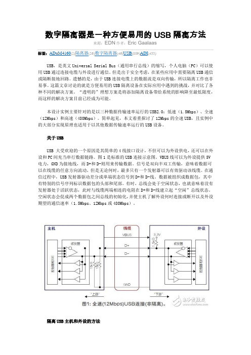
图1是标准的USB连接示意图。
VBUS线可以为外设提供5V 电力,GND为接地线,而D+和D-则用来传输数据。
信号是双向半双工传输,意味着数据可以在线缆的任意方向流动,但是无论何时,最多只有一个发射器可以有效驱动该线缆。
在通信过程中,USB发射器驱动差分或单端状态信号到D+和D-线。
数据被组织成数据包,其中有特别的信号序列标识数据包的头部和尾部。
有时,总线会处于空闲状态,也就意味着没有发射器处于活跃状态,此时与线缆两端相连的电阻在D+和D-线建立起“空闲”总线状态。
空闲状态会促成两个数据包之间总线的初始化,并使主机了解外设何时连接或断开以及外设期望的通信速率(1.5Mbps、12Mbps或480Mbps)。
隔离USB主机和外设的方法现在想象一下对主机和外设进行电气隔离的方法。
ADI磁耦数字隔离器原理介绍

由图中可以看出,输入的信号经过一个施密特触发器进行脉冲信号调整,使输入的波形为标准的矩形波。另磁耦还独具直流较正功能,图中的两组线圈起到脉冲变压器的作用,输入端逻辑电平的变化会引起一个窄脉冲(2ns),经过脉冲变压器耦合到解码器,然后再经过一个施密特触发器的波形变换输出标准的矩形波,如果输入端逻辑电平超过2US都没有任何变化,则校正电路会产生一个适当极性的校正脉冲,以确保变压器直流端输出信号的正确性,如果解码器一端超过5US都没有收到任何校正脉冲,则会认为输入端已经掉电或不工作,由看门狗电定时器电路,将输出端强行置为高电平。
ADI
贴子发表于:2009/2/4 11:02:55
磁耦是一种数字隔离器,可替代光耦,并在速度、耐温、使用性能等各方面都优于光耦。
与光耦不同,磁耦是基于芯片级的变压器隔离技术,没有经光耦的光电转换过程。并且体积远远小于、通讯、A/D转换、PDP、等各种系统中。
隔离器如何选型-数字隔离器选型步骤

隔离器如何选型-数字隔离器选型步骤(总4页)--本页仅作为文档封面,使用时请直接删除即可----内页可以根据需求调整合适字体及大小--隔离器如何选型?数字隔离器选型步骤是,不知如何去选择一个合理的、适用的隔离器。
前两天,记者采访了ADI公司数字隔离器产品高级应用工程师周晓奇,他就有关隔离器在电路中的作用、工程师在数字隔离器选型时应该注意哪些步骤等问题,给电子工程师们一个很好的解答。
为什么要用隔离器隔离器主要是用在隔离高压(危险电路)系统和低压(安全电路)系统之间的电气连接,以保护用户以及电路系统安全,以及隔离敏感电路(比如高精度检测电路)和噪声源(例如大功率开关电源)之间的连接,以减小噪声干扰。
周晓奇说,隔离器的主要结构大致有四种:一是传统光电耦合; 二是集成式变压器(磁耦合);三是集成式电容耦合; 四是分立式变压器耦合。
最常用的是光耦合器,光耦合器一般由三部分组成:光的发射、光的接收及信号放大。
输入的电信号驱动发光二极管(LED),使之发出一定波长的光,被光检测器接收而产生光电流,再经过进一步放大后输出。
它的主要优点是单向传输信号,输入端与输出端完全实现了电气隔离,抗干扰能力强,使用寿命长,传输效率高。
它广泛用于电平转换、信号隔离、级间隔离、开关电路、远距离信号传输、脉冲放大、固态继电器(SSR)、仪器仪表、通信设备及微机接口中。
随着近几年数据传输的速度不断提升,传统的光耦合器也暴露出一些缺点,例如,整个电路体积大,集成度不高,而且光电耦合器件本身具有易损耗、速度较慢(一般的数据速率低于1Mbps)、耗电量大等缺点,特别是在温度和老化变化过程中的性能极不稳定,为其应用带来局限,特别是在工业应用中这些问题就比较突出。
为了克服光电隔离技术的诸多缺点,许多半导体公司开始研发不发光的隔离器解决方案。
周晓奇告诉记者,ADI 公司是最早一家推出新型数字隔离器解决方案的公司,并于2001年率先推出基于其专有iCoupler磁耦隔离技术的标准数字隔离产品。
磁隔离

磁隔离是ADI公司iCoupler® 专利技术,是基于芯片级变压器的隔离技术。 磁耦
磁耦是基于iCoupler磁隔离 技术的隔离器件,也称为磁隔离器。
iCoupler磁隔离可以在低成本条件下实现多通道及其他功能集成。iCoupler磁隔离变压器采用平面结构, 在晶圆钝化层上使用CMOS金属和金构成。金层下有一个高击穿的聚酰亚胺层,将顶部的变压器线圈与底部的线圈 隔离开来。连接顶部线圈和底部线圈的CMOS电路为每个变压器及其外部信号之间提供接口。晶片级信号处理提供 了一种在单颗芯片中集成多个隔离通道以及其它半导体功能的低成本的方法。iCoupler磁隔离技术消除了与光耦 合器相关的不确定的电流传送比率、非线性传送特性以及随时间漂移和随温度漂移问题;功耗降低了90%;并且 无需外部驱动器或分立器件。
长寿命
采用芯片级变压器技术传输信号,消除光耦传输时的器件损耗。器件内部基本不存在损耗,正常工作条件下 至少达到50年工作寿命。
高性能
磁耦能够在低功耗的条件下实现150Mbps的高速数据隔离,光耦鲜有如此高的传输速率,实现同样高的传输 速度,磁耦比光耦有着更高的性价比。磁耦芯片内部含有施密特电路,能够对输入输出的电路滤波整形,因此可 直接与各种高速控制芯片直接连接,如:DSP、ARM、PLC等。
磁隔离
基于芯片级变压器的隔离技术
01 技术03 分类 05 现状目录02 原理 04 优势
基本信息
iCoupler磁耦隔离器是基于芯片尺寸变压器的磁耦合器,与传统光耦合器中采用的发光二极管(LED)和光 电二极管不同,iCoupler磁隔离技术通过采用晶圆级工艺直接在片上制作变压器。
技术
技术
易用性
磁耦的小体积及多种通道配置,是电路设计更加简洁,应用更加灵活。集成的多种接口收发器使得接口隔离 电路集成度更高,线路连接大大减少。
ADI推出业界最低功耗数字隔离器
ADI推出业界最低功耗数字隔离器北京2013年11月19日电- Analog Devices, Inc. (NASDAQ: ADI)最近推出业界功耗最低的数字隔离器 -- ADuM144x系列。
ADuM144x基于ADI专有i Coupler数字隔离技术,可由低至1 uW的功率供电,其功率水平比光耦合器和数字隔离器竞争产品降低了1,000多倍。
因此,ADuM144x系列非常适合用于工业和仪器仪表系统,例如4-20 mA电流环路、远程传感器,以及需要高能效或依赖电池等受限制电源的绿色系统。
欲了解ADuM144x低功耗数字隔离器的更多信息,请观看视频:/ADuM144xvideo 。
ADI推出业界最低功耗数字隔离器欲订购ADuM144x样片、下载数据手册和其他技术文档,请访问:/zh/pr1119/adum144x欲让ADI中文技术论坛EngineerZone™上的ADI工程师为您解答数字隔离器相关的问题,请访问/community/interface-isolation更多有关产品信息,请致电亚洲技术支持中心:400 6100 006, 或发送邮件至china.support@,也可点击ADI官方微博/analogdevices ,或通过手机登录m. 或了解最新产品等信息。
更多ADI产品及应用视频,请访问:/category/chinese/产品目录上的授权代理商Digi-Key Corp和Mouser Electronics均有芯片和评估板库存现货。
ADuM144x是四通道数据隔离器,提供三种不同的通道配置,其一分钟的安全隔离额定值为2.5 kV rms。
ADuM144x的工作电压范围为2.25 V至3.6 V,不仅进一步降低了功率限制,而且提供了市场上最低的工作电压。
电压为2.5 V时静态电源电流小于每通道5。
uA,速率为2 Mbps时电源电流小于每通道380 μA。
1.ADI的数字隔离器基础知识
2
The Isolation Function
Galvanic
Isolation – No Current Flow
Isolator
Point B
Information Flow No Current Flow Isolation Barrier Typical Application Characteristics High Voltage High-Precision Communications Long-Distance Communications
Wear
out Accelerated by:
Increased current Most are rated to 85C Higher Temperature ratings increase price and reduce speed
9
Chip-Scale Transformer Isolation
Transformer and Package Provide Up To 5 kV rms Isolation
Direction of Isolation Barrier
Transformer Chip
iCoupler Technology Background
Polyimide Isolation
standard for low-cost isolation
GaAs
or GaAlAs LEDs emit light when current passes through it
5-20mA
typically used Speed is directly correlated to current
ADuM1100_CN
Http://
第6页/共 6 页
※兼容 VDD1=3V,V DD2=5V 以及 VDD1=5V,V DD2=3V 的工作模式。
五、芯片引脚配置和功能描述
图 2,ADuM1100 引脚图
Http://
第3页/共 6 页
ADuM1100
引脚 1 2 3 4 5 6 7 8 名称 VDD1 VI VDD1 GND1 GND2 VO GND2 VDD2 功能描述 逻辑端供应电源输入 3.0~5.5V 逻辑输入 逻辑端供应电源输入 3.0~5.5V 逻辑端参考地 隔离端参考地 逻辑输出 隔离端参考地 隔离端供应电源输入 3.0~5.5V
第4页/共 6 页
ADuM1100
4、脉宽失真
脉宽失真 P W D (pulse-width distortion) 是指低至高延迟时间 TPLH 与高至低延迟时间 TPHL 之间的最大差值,它显示了器件经过器件输出后保持原样的精确程度。
5、 直流校正功能
磁隔离器每一通道的两组线圈起到脉冲变压器的作用,输入端逻辑电平的变化会引起 一个窄脉冲(2ns) ,经过脉冲变压器耦合到解码器,然后再经过一个施密特触发器的波形变 换输出标准的矩形波, 如果输入端逻辑电平超过 1µs 都没有任何变化, 则校正电路会产生一 个适当极性的校正脉冲,以确保变压器直流端输出信号的正确性,如果解码器一端超过 5µs 都没有收到任何校正脉冲,则会认为输入端已经掉电或不工作,由看门狗电定时器电路,将 输出端强行置为高电平。这确保了磁隔离可以传输直流信号。
有关数字隔离器的七大设计问题
有关数字隔离器的七大设计问题作者:德州仪器Luke Trowbridge您是否正在搜寻有关数字隔离器的更多信息?我们将为您提供帮助。
根据TI E2E™社区的反馈,我们搜集并整理了关于数字隔离器设计攻关的最常见问题清单。
希望这份清单能为您提供隔离信号与电源的有用见解。
1.基础型和增强型数字隔离器至简的区别是什么?基础型数字隔离器必须根据组件级标准,通过一套测试,如Deutsches InsTItut für Normung (DIN)V Verband der Elektrotechnik,Elektronik und InformaTIonstechnik (VDE)V 0884-11。
DIN V VDE V 0884-11 定义了隔离器可以耐受的电压水平,比如最大浪涌隔离电压,VIOSM;最大瞬态隔离电压,VOITM;及最大重复峰值隔离电压,VIORM(参见白皮书“高压增强型隔离:定义与测试方法”中的解释)。
增强型数字隔离器,除通过这些测试外,还必须通过最小浪涌电压测试等级10,000 VPK.测试。
2.能为数字隔离器两端施加不同的电压吗?可以。
数字隔离器可以在建议的工作条件下为设备两端供电。
由于隔离势垒隔离了两端,每端均可在建议的工作条件下独立施加任意电压值。
举例来说,可以为ISO7721 施加3.3 V VCC1(在2.25 V - 5.5 V 之间)和5 V VCC2(也在2.25 V - 5.5 V 之间)。
除构建隔离外,通过这种方法,您还可以把数字隔离器用作逻辑电平转换器。
隔离器两端相互独立。
3.数字隔离器信号电压可以异于它的电源电压吗?不能。
数字隔离器的输入/输出信号电压取决于它的电源电压。
因此,如果要使数字隔离器兼容它所对接的设备,最好是保持信号电压与隔离器电源电压相同。
例如,如果ISO7721 的电源电压为5 V,它对接微控制器(MCU),那么很重要的一点就是MCU 信号也工作在5V 逻辑电平。
隔离卡注意事项及各种故障解决方法

注意事项
⏹与隔离卡相连的三根IDE 数据线最好要统一,即全部是UDMA33或
UDMA66,(通常所说的低密线和高密线)否则会造成信号传输不匹配。
⏹注意IDE 数据线的连接顺序,IDE 数据线的1端(蓝色)一般连接主
板或者隔离卡的内网、外网的IDE口,IDE 数据线的2、3端(黑色)
一般连接硬盘或者隔离卡的TO PC IDE口。
⏹在Dell计算机上安装要注意的问题:
⏹因为Dell计算机的BIOS比较与众不同,所以安装时需要在有些方面注
意:
⏹在进行硬盘克隆的时候,要先把BIOS中的第二硬盘选项打开,否则不
能发现新装的硬盘;
⏹在克隆完成后,要先进入BIOS中把BIOS中的第二硬盘选项关闭,否
则在直接摘掉硬盘后,系统启动前会有一长段时间进行硬件检测,造成
一种假死机现象;
⏹如果有可能需要修改Power on self test.(需要把Quick改为Enhanced)、
Fast Boot.(需要把On改为Off)
⏹西数80G硬盘:
⏹西数80G硬盘要把全部跳线拔掉后才是Master方式。
遇到西数硬盘时
注意看一下硬盘背面的跳线图,看清跳线方式。
⏹在安装联想机器的时候要特别注意,联想的BIOS有部分是屏蔽的,无
法显示UDMA选项,这时试用Ctrl+F1进入,可以显示出所有BIOS选
项。
【下载本文档,可以自由复制内容或自由编辑修改内容,更多精彩文章,期待你的好评和关注,我将一如既往为您服务】。
隔离卡介绍及常见故障处理

背景
• 隔离卡最早起源于1999年,当互联网正兴起时。 由于操作系统、CPU、内存等这些核心技术都不在中 国,数据放在操作系统之上,而操作系统的源代码不 了解,就会出现风险。这时就应运而生提出了物理隔 离的概念:“处于不同安全域的网络之间不能以直接 或间接的方式相连接。在一个物理网络环境中,实施 不同安全域的网络物理断开,在技术上应确保信息在 物理传导、物理存储上的断开。” • 同年国家保密局确定发文《关于加强政府上网信 息保密管理的通知》(国家保密局国保发行(1999) 4号)要求:“涉密信息网络必须与公共信息网实行 物隔离,在与公共信息网相连的信息设备上不得存储、 处理和传递国家秘密信息。”
3、安装隔离卡后硬盘不能正确识别
(1)去除隔离卡,看系统能否检测到硬盘,如不能检测到 硬盘,则问题与隔离卡无关。 (2)数据线控制隔离卡:调整各硬盘跳线方式,更改隔离 卡连接到主板上的IDE插槽;如果是SATA硬盘,更改隔离 卡连接到主板上的SATA插槽,并将BIOS中相应选项设置为 “SATA ONLY”;使用尽量短的数据线。 (3)电源线控制隔离卡:如果是两块SATA硬盘,尽量将两 块硬盘连接到主板上的呈对角的SATA插槽上,并将BIOS中 相应选项设置为“SATA ONLY”;如果是IDE硬盘,更改硬盘、 光驱的跳线方式,以及在IDE线上的位置,两个硬盘跳线 不一定一致。
5、无法连接网络
(1) 请检查内外网线是否插在相应的插座上,有否松 脱。 (2)请检查连接网络安全隔离卡和网卡的连接跳线是 否连接正确或松脱。 (3)将内网线或外网线直接插入网卡接口,如果故障 现象仍然存在,则故障与网络安全隔离卡无关,请检查 其它网络设备、网线、墙壁上的网线插座。
谢谢!
电源隔离
数字隔离器原理

数字隔离器原理数字隔离器是一种常见的电子设备,用于将数字信号从一个电路隔离到另一个电路,以保护电路之间的互联和通信。
它在工业控制系统、通信设备和电子仪器中广泛应用。
本文将介绍数字隔离器的原理和工作方式。
一、数字隔离器的基本原理数字隔离器的基本原理是利用光电耦合器或磁耦合器将输入信号和输出信号隔离开来。
光电耦合器是一种将输入光信号转换为输出电信号的器件,而磁耦合器则是利用磁场的作用将输入信号和输出信号隔离开来。
二、数字隔离器的工作方式数字隔离器通常由输入端、输出端和隔离器件组成。
输入端接收来自源电路的数字信号,经过隔离器件的处理后,输出端将隔离后的信号传递给目标电路。
在光电耦合器中,输入端的光信号通过发光二极管产生,并经过光电二极管转换为电信号。
这样,输入信号和输出信号之间就通过光信号进行了隔离。
在磁耦合器中,输入信号通过输入线圈产生磁场,磁场作用于输出线圈,从而在输出端产生电信号。
这样,输入信号和输出信号之间就通过磁场进行了隔离。
三、数字隔离器的优势数字隔离器具有以下几个优势:1. 隔离性能好:数字隔离器能够有效地隔离输入信号和输出信号,避免干扰和噪声的传递。
2. 电气隔离:数字隔离器能够实现电气隔离,避免电流和电压的传递,提高系统的安全性。
3. 抗干扰能力强:数字隔离器能够有效地抵御外界的电磁干扰和噪声,保证信号的稳定性和可靠性。
4. 传输速度快:数字隔离器能够实现高速的信号传输,满足现代工业控制和通信系统对高速传输的需求。
四、数字隔离器的应用领域数字隔离器广泛应用于以下领域:1. 工业控制系统:数字隔离器在工业自动化控制系统中起到了重要的作用,用于隔离控制信号和传感器信号,保护控制系统的稳定性和可靠性。
2. 通信设备:数字隔离器在通信设备中用于隔离输入信号和输出信号,保护通信设备免受电气干扰和噪声的影响。
3. 电子仪器:数字隔离器在电子仪器中用于隔离输入信号和输出信号,保护仪器的精度和稳定性。
狄耐克各系统配置及一般故障

说明:(1)隔离器引起分机无光栅一般为:各端口中大功率三极管 772 坏或供电电源良。 (2)分机无光栅一般是 CRT 坏。
6、门口主机呼叫分机无图像
门口主机呼叫分机无图像
是否整梯无图像
其中一层无图像
是 否 主干视频线 接好
是否接好
是
视频主干线上 是否有信号
只有一户无图像
分户视频线 否 接好
是否接对
六芯联网空中对插线是否接对、接好
是 更换门口主机是否能排除故障
是 换门口主机
15、围墙机不能呼叫管理中心
围墙机不能呼叫管理中心
否 围墙机(602 )到多门选择器 接好
(602 )之间连接线是否接对、接好
是
供电 否 多门选择器(602 )是否有供电(+18 )
(+18 )
是
更换多门选择器 是 替换多门选择器(602 )
隔离器
2.黑 GND 401
3.黄 HOOK 4.绿 AUDIO
2F
202
5.棕 DOOR
6.橙 CALL
RVV6x0.3 101
隔离器
401
1F
102
RVV2x0.75 UPS-P
联网主干线 RVVP3x0.75
RVV2x0.75 UPS-DP
电控锁
RVV3x0.5 1.绿 AUDIO
2.棕 DATA 3.橙 GND
隔离器
2.黑 GND
2.黑 GND
402
3.黄 HOOK 3.黄 VIDEO
2F
202
4.绿 AUDIO
5.棕 DOOR
6.橙 CALL
RVV7x0.3+SYV-75-3
隔离器
数字电源中的隔离—原因及方式
数字电源中的隔离—原因及方式随着互联网和通信基础设施的蓬勃发展,数字控制技术在电信、网络和计算机的电源系统中越来越受欢迎,因为这类技术具备灵活性、器件数量减少、先进的控制算法、系统通信、对外部噪声和参数变化不太敏感等极具吸引力的优势。
数字电源广泛用于高端服务器、存储、电信砖式模块等经常会有隔离需求的应用。
隔离在数字电源中的挑战是在紧凑的面积下如何快速准确地传输数字信号或模拟信号通过隔离边界。
1 然而,传统光耦的解决方案有带宽比较低,电流传输比(CTR)会随温度和时间发生大幅变化等问题。
而变压器的解决方案有体积庞大、磁饱和等问题。
这些问题限制了光耦合器或变压器在某些高可靠性应用、紧凑型应用以及长寿命应用中的使用。
本文讨论利用ADI公司iCoupler®产品的数字隔离技术,来解决在数字电源设计中遇到的这些问题。
需要隔离的原因在设计电源时,遵守安全标准对于保护操作人员及其他人员免受电击和有害能量的侵害至关重要。
隔离是满足安全标准要求的重要方法。
许多全球机构(比如欧洲的VDE和IEC以及美国的UL)规定了不同输入和输出电压(稳态和瞬态)水平的隔离要求。
例如,在UL60950中介绍了五类绝缘:功能绝缘:仅在设备正常运行时需要的绝缘。
基本绝缘:提供基本电击防护的绝缘。
补充绝缘:基本绝缘外的独立绝缘,用于在基本绝缘发生故障的情况下降低电击风险。
双重绝缘:包括基本绝缘和补充绝缘的一种绝缘。
加强绝缘:一种单一绝缘系统,提供一定程度的电击防护,在本标准规定的条件下相当于双重绝缘。
原边控制与副边控制对比根据控制器的位置,隔离电源控制方式分为原边控制和副边控制两种。
表1对比了原边控制和副边控制的功能。
在下表中,UVP和OVP分别代表欠压保护和过压保护。
表1. 原边控制与副边控制的功能对比副边控制ADP1051是ADI公司先进的数字电源控制器,具有PMBus™接口,面向中间总线转换器等高功率密度和高效率应用。
2ADP1051基于灵活的状态机架构,提供众多颇具吸引力的特性,比如反向电流保护、预偏置启动、恒流模式、可调输出电压压摆率、自适应死区时间控制以及伏秒平衡,与模拟解决方案相比,减少了大量的外部元件。
【E问E答】数字电路一些常见问答
【E问E答】数字电路一些常见问答
了解数字电路的隔离技术,对以后设计有很好的帮助,下面大家一起来看看。
ADI 的全集成式RS-485 系统隔离解决方案
iCoupler 技术一直引领全球隔离技术的发展,提供了隔离与创新特性,采用单封装,是业界种类最齐全的隔离器产品,包括标准数字隔离器、采用isoPower 的数字隔离器、集成PWM 控制器和变压器驱动器的数字隔离器、USB 2.0 兼容型隔离器、隔离式门驱动器、隔离式I²C 数字隔离器、隔离式RS-485 收
解析电磁兼容中的隔离技术
电力电子设备包括两部分,即变换部分与控制部分。
前者属于功率流强电范畴,后者属于信息流弱电范畴。
一般情况下前者是主电磁干扰源,后者是被干扰对象。
为了使电力电子设备可靠地运行,除了解决变换部分与控制部分之间的电气隔离外,还要解决控制部分的抗电磁干扰的问题,特别是当变换部分处于高电压、强电流、高频变换情况
电磁脉冲对数字电路的辐照效应研究
为研究电磁脉冲对数字电路的辐照耦合规律,介绍了雷电电磁脉冲的模拟装置并以某装备上信息处理的串行数据分配电路为试验研究对象,研究了磁脉冲辐射场对数字电路的辐照效应,通过改变场的强度、极性、被试器件的类型等试验条件,探讨了电磁脉冲对数字电路的耦合规律。
试验结果表明:影响电磁脉冲对电路的辐照耦合的因素有场的强度、接收天线形状、器件电路的内部结构与阻抗特性、设备或系统在电磁场中的方向、以及线上的信号(即高或低电平信号)等。
- 1、下载文档前请自行甄别文档内容的完整性,平台不提供额外的编辑、内容补充、找答案等附加服务。
- 2、"仅部分预览"的文档,不可在线预览部分如存在完整性等问题,可反馈申请退款(可完整预览的文档不适用该条件!)。
- 3、如文档侵犯您的权益,请联系客服反馈,我们会尽快为您处理(人工客服工作时间:9:00-18:30)。
FAQ: Isolation, i Coupler® Technology, and i Coupler ProductsIsolationWhat is isolation? Why is it needed?What are common applications that use isolation?How is isolation specified?What is isolation rating?What are working voltage and rated mains voltage?What is the relationship between working voltage and isolation rating?What is the difference between basic and double (or reinforced) insulation levels?What are transient immunity and common-mode rejection?What other parameters are important when considering an isolation device?Regulatory StandardsWhat regulatory standards address isolation products?Traditional Isolation TechnologiesWhat types of technologies have been used to provide isolation?What are optocouplers? What is optical isolation?What is transformer isolation?What is capacitive isolation?i Coupler TechnologyWhat is i Coupler technology?What are the benefits of i Coupler technology?How much isolation can i Coupler products provide?With which regulatory standards do i Coupler products comply?Do i Coupler products have VDE certification for reinforced insulation?Are i Coupler products sensitive to external magnetic fields?i Coupler ProductsWhat are the different types of i Coupler products?Which i Coupler product is best for my application?What communications protocols are supported by i Coupler products?What are some of the distinguishing features of the i Coupler products?Can I replace an optocoupler with an i Coupler product in an existing design?How do i Coupler products differ from interface products?Does Analog Devices provide other products that employ i Coupler technology?Are i Coupler products Pb-free?How do I learn about new i Coupler products?iso Power™What is iso PowerWhat are common applications of iso Power?How does iso Power work?What are the benefits of iso Power?How much power do iso Power products supply?What iso Power products are currently in production?SupportWhere can I find support for designing with ADI's i Coupler products?I did not purchase i Coupler products from Analog Devices or an authorized distributor — how can I get support?What do the i Coupler product datasheets guarantee?What tools or models exist to support my design?back to topIsolationWhat is isolation? Why is it needed?Isolation is a means of preventing current from flowing between two communicating points. Typically, isolation is used in two general situations. The first is where there is the potential for current surges that may damage equipment or harm humans. The second is where interconnections involve different ground potentials and disruptive ground loops are to be avoided. In both cases, isolation is used to prevent current flow yet allow for data or power flow between the two points.What are common applications that use isolation?Isolation is commonly found in applications involving high voltage, high-speed/high-precision communications, or communication over large distances. Common examples of such applications include:q Industrial I/O systemsq Sensor interfacesq Power supply/regulation systemsq Motor control/drive systemsq InstrumentationThese applications can be found in a wide range of markets, including:q Medical equipmentq Communication networksq Plasma display panelsq Hybrid automotive vehiclesHow is isolation specified?The isolation characteristics of an isolator are specified in a variety of manners, including:q Isolation ratingq Working voltage (or rated mains voltage)q Transient immunity (common-mode rejection)The degree to which an isolator successfully insulates one side of an isolation barrier from high voltages on the other side is commonly described by the isolator's isolation rating and by its maximum working voltage (or rated mains voltage). In addition, the degree to which an isolator continues to correctly transfer a signal across an isolation barrier in the presence of a common-mode transient is described by its transient immunity (or common-mode rejection). Each of these three parameters is described below.What is isolation rating?An isolator's isolation rating (also called the test voltag e) is a measure of the protection provided against short-duration, common-mode voltage differences. Usually specified in terms of a 60 Hz RMS value, it is a rating of how much voltage can be safely applied between the input and output terminals of the device for a duration of one minute. A common isolation ratingfound on isolation devices is 2.5KV RMS. Other devices have ratings such as 3.75KV RMS or higher. The isolation rating does not describe how much voltage can be safely applied across the part on an long-term continuous basis – this is described by the "working voltage" or "rated mains voltage."What are working voltage and rated mains voltage?The working voltage or rated mains voltage defines the maximum steady-state voltage that a part can support on a long-term continuous basis. Typical values range from 100 to 600V RMS.What is the relationship between working voltage and isolation rating?The relationship between a given working voltage and the required test voltage is complex and is a function of the application, the magnitude of common-mode voltage transients (Installation Category), the "cleanliness" of the environment (Pollution Degree), and the required insulation type (Insulation Level). As a representative example based on IEC 1010-1 (international standard for measurement and control equipment), a measurement and control application involving installation category II, a pollution degree of 2, basic insulation, and a working voltage of 300 V RMS has a required test voltage of 1.35KV RMS. This means that for an isolation component to be suitable for this application, it must support steady-state common-mode voltages differences of at least 300 V RMS and transient common-mode voltages differences of at least 1.35KV RMS. The relationship between working voltage and isolation rating is defined by the specific safety standard for the end-equipment under consideration.What is the difference between basic and double (or reinforced) insulation levels?In general, protection against electric shock may be provided by adequate clearance (a physical spacing from the live part) or by one of two insulation levels. These insulation levels are basic insulation and double (or reinforced) insulation. The required insulation level is determined by the voltage levels involved as well as the presence or absence of a connection from accessible parts to earth ground. In general, compared to an isolator providing basic insulation, an isolator providing double or reinforced insulation has greater requirements on its test voltage as well as on its input-to-output spacing. The required insulation level is defined by the specific safety standard for the end-equipment under consideration.What are transient immunity and common-mode rejection?An isolator's transient immunity specifies how fast of a common-mode transient between input and output a part can be subjected to while maintaining correct signal transmission. Many isolators have no specification on this parameter while others have values ranging from 5 to 25 KV/µs. All i Coupler products have a transient immunity specification of at least 25 KV/µs.What other parameters are important when considering an isolation device?The ideal isolator consumes no power, imposes no signal errors, and supports any type of input signal. As a result, the important performance metrics are as follows:q Required supply current, input signal current, or input drive currentq Propagation delay through the partq Pulse width distortion: the degree to which the output pulse width of a signal varies from the input pulse widthq Data rate: the maximum signal data rate that the part can supportq Supply and signal voltage range: the range of voltages that the part can supportq Operating temperature: the range of temperatures that the part can supportWhich of the above metrics are important to a particular user is a function of the application in question. Often in a specific application, certain parameters are important and others are not.Other performance characteristics important to users are an isolator's power-up/down characteristics, its performance in the presence of input noise, and its performance in the presence of a DC input or after a loss of power. In all cases, the output of an isolator should properly reflect the correct input state.back to topRegulatory StandardsWhat regulatory standards address isolation products?There are a wide variety of safety standards related to isolation at both the system and component levels, for various geographic regions, and for various applications. Shown below is a table summarizing commonly-used standards for the U.S., Europe, and International geographic regions.Table 1. Application-Level Standards.Industrial UL 508EN 50178IEC 604Information Technology UL 1950EN 60950IEC 950Medical UL 2601-1EN 60601IEC 601 Measurement and Control UL 3111EN 61010-1IEC 1010-1Telecom UL 1459EN 60950IEC 950Household UL 8730-1EN 60065IEC 65Table 2. Component-Level Standards.Isolator UL 1577Component AcceptanceNotice #5DIN EN60747-5-2DIN V VDE V 0884-10IEC 747-5The standards that apply directly to isolation components are those of Table 2. The standards of Table 1 apply to applications that use isolation components. The designer of such an application must assure that the appropriate isolation component is selected such that compliance with the relevant application-level standard is ensured. However, the application-level standard is not directly applicable to the isolation component. Only the standards of Table 2 are imposed directly at the component level.back to topTraditional Isolation TechniquesWhat types of technologies have been used to provide isolation?There are three common isolation technologies:q Opticalq Transformerq CapactitiveEach has benefits and disadvantages related to price, performance, reliability, size, features and functionality. Historically, optocoupler and transformer technologies have been the most commonly used methods.What are optocouplers? What is optical isolation?Optocouplers are a form of optical isolation that employs light to transmit information across an isolation barrier. Typically, a light emitting diode (LED) transmits information to a light sensitive receiver (e.g., a transistor). Optical isolation's primary benefit is that it is widely used and accepted as a low-cost isolation solution for transmission of slower digital signals; high-speed, digital optocouplers tend to be expensive. Optocoupler-based methods are commonly used in applications in which the DC state of a signal is important. Because LEDs may wear out over time, optical isolation typically requires compensation and guardbanding to guarantee application operability over life.What is transformer isolation?Transformer isolation employs transformer coils to transmit information across an isolation barrier. Changes in current through the transformer winding on one side of the isolation barrier induce a corresponding current on the transformer winding on the other side of the isolation barrier. Transformer-based methods have been commonly used in applications involving AC signals (Ethernet, for example) that are well suited for transformer coupling. Transformer isolation has advantages in systems with high data rates, and it can also be used to provided an isolated power supply; however, transformers have typically been bulkier than alternative solutions.i Coupler technology (see below) is a form of transformer isolation that employs micro-transformer coils to address the size and integration disadvantages of discrete transformer solutions.What is capacitive isolation?Capacitive isolation employs capacitors to couple data signals across an isolation barrier. This approach can offer significant performance advantages relative to optocoupler but typically suffer a high vulnerability to common-mode and ESD transients.back to topi Coupler TechnologyWhat is i Coupler technology?i Coupler technology is a transformer-based approach to isolation that combines the advantages of optocoupler, transformer, and semiconductor technologies. By integrating micro-transformers onto semiconductor dice, isolation is provided without the detrimental characteristics of the electro-optical conversions present in optocouplers. These include excessive power consumption, large timing errors, and constraining data rate limitations. Safety agency-recognized insulation is achieved through the used of a special insulation layer between the transformer coils. The common transformer problem of achieving DC-correctness is avoided by the use of patented "refresh" circuitry that updates the output with the correct input state in the absence of input signal transitions.What are the benefits of i Coupler technology?i Coupler technology provides benefits in five key areas:q Integration (size/cost)q Performanceq Power consumptionq Ease-of-useq ReliabilityIntegration benefits are provided by the ability to readily combine i Coupler channels with other semiconductor functions or to combine multiple i Coupler channels in a common package thereby reducing size and cost relative to optocoupler implementations. Performance benefits are provided in the form of increased timing accuracy, transient immunity, and data rates relative to optocoupler components. Power consumption benefits are provided in the form of 10-to-50 times lower power consumption as well as the accompanying reduction in thermal dissipation.Ease-of-use benefits are provided by the elimination of many of the difficulties presented by optocoupler technology as well as the addition of new features that facilitate the use of i Coupler isolators in new designs. Optocoupler problem areas thati Couplers eliminate include their characteristic of widely-varying current transfer ratios, their LED wear-out phenomenon and the design burdens this imposes, and their need (in most optocouplers) to drive their input with high current to turn on the LED. Additional ease-of-use features that i Couplers provide include the ability to operate at reduced supply voltages, the ability to translate an input signal of one voltage into an output signal of a different voltage, the use of voltage-based digital interfaces, and the ability to operate over a wide temperature range.Lastly, reliability benefits are achieved by the elimination of the LEDs contained within optocouplers. By using only standard CMOS process technology, i Coupler devices provide the same lifetime characteristics as other standard CMOS products.How much isolation can i Coupler products provide?As of this writing, most i Coupler products carry an isolation rating of either 2.5KV RMS or 5.0KV RMS (the ADuM240x andADuM225x isolators carry an isolation rating of 5.0KV RMS). The maximum working voltage that i Coupler products support is a function of both the safety approvals a given product has as well as its insulation lifetime as evaluated by testing performed by Analog Devices in addition to that of the safety agencies.All i Coupler products support working voltages up to 400 V RMS. The ADuM240x and ADuM225x families support higher working voltages.The maximum working voltage supported by the ADuM240x or ADuM225x depends on the nature of the common-modewaveform that is imposed across the isolation barrier. This is due to the fact that the i Coupler insulation system is stressed differently for the various waveforms shown below. In the case of bipolar AC waveforms, the maximum working voltage is set by the criteria that the insulation have a 50 year minimum lifetime. In the case of other types of voltage waveforms, the maximum working voltage is limited by regulatory safety approvals – despite the insulation's ability to withstand higher voltages with a 50 year minimum lifetime. The table below summarizes the maximum recommended voltages for the ADuM240x and ADuM225x as a function of waveform type:Table 3: ADuM240x and ADuM225x Maximum Working VoltagesAC Voltage, Bipolar Waveform400 V RMS (565 (V PK)50-year minimum lifetimeAC Voltage, Unipolar Waveform519 V RMS (848 (V PK)Maximum CSA/VDE approved working voltage DC Voltage848 V PK Maximum CSA/VDE approved working voltageWith which regulatory standards do i Coupler products comply?i Coupler products typically carry at least a 2.5 kV RMS UL rating and a 400 VRMS working voltage approval from CSA and UL. The approvals and details for each specific product are summarized in the table available at /iCouplerSafety.Do i Coupler products have VDE certification for reinforced insulation?Yes. i Coupler products have now been approved for reinforced insulation by VDE. Until recently, no VDE standard covered reinforced insulation for magnetic couplers such as the i Coupler family of digital isolators; however, VDE released DIN V VDE V 0884-10 (VDE V 0884-10) in December 2006, and i Coupler products successfully completed testing to this standard. For details about specific working voltages and isolation ratings for each i Coupler product, and to view the safety certificates, please visit /iCouplerSafety.Are i Coupler products sensitive to external magnetic fields?No – unless such fields are extremely strong and of high frequency. Since the transformers used within i Coupler devices typically measure about 0.5 mm in diameter, it takes a very high magnetic field rate-of-change to induce a voltage large enough to cause a performance error. For example, if a wire carrying a current oscillating at 1 MHz were to be placed 5 mm away from an i Coupler transformer, the current amplitude that would be required in order to cause a problem with the i Coupler's performance is 500A! (An analysis of this can be found in the Applications section of any i Coupler data sheet.)back to topi Coupler ProductsWhat are the different types of i Coupler products?i Coupler products are available in a variety of channel configurations and performance levels. Products consists of single, dual, triple, and quad channel 2.5KV RMS and 5.0KV RMS isolators each available in multiple performance/price options. Products arealso offered with other features including:q High Speed (150 Mbps) Quad Isolators (ADuM344x)q Default Low or Programmable Default Output (ADuM1210, ADuM131x, ADuM141x)q Increased EOS/ESD robustness (ADuM3100, ADuM320x, ADuM330x, ADuM340x)q Isolated power (see iso Power below) (ADuM524x)q Dual and quad gate drivers (ADuM1233, ADuM1234)2C (ADuM125x, ADuM225x)q Iq RS-485 (ADM2483, ADM2485, ADM2486, ADM2490E)qΣ∆ Modulator (AD7400, AD7401)Please refer to the i Coupler web site (/icoupler) for the most complete up-to-date selection table and other information about the iCoupler portfolio.Which i Coupler product is best for my application?Due to the unique nature of each application, the choice of which product to use is best left to the user. The selection tables available at /iCoupler should provide guidance for choosing the most appropriate i Coupler product. For additional assistance, please contact your local Analog Devices sales representative or distributor.What communications protocols are supported by i Coupler products?i Coupler products are capable of supporting most standard communications protocols but may require additional components to ensure communication integrity. Products such as the ADuM1401 are ideal for SPI where four channels are required for Clock, Data In, Data Out, and Select.The ADuM125x and ADuM225x have been designed for compliance to the I2C, PMBus and SMBus protocols.The ADM2483, ADM2485, ADM2486 and ADM2490E are complete isolated RS-485 solutions.What are some of the distinguishing features of the i Coupler products?Distinguishing features of i Coupler products include integration that optimizes cost and size as well as the ability to support high signal data rates and the ability to operate with extremely low supply currents. i Coupler products provide an excellent cost/size advantage over competing alternatives due to integration of multiple channels as well as other functions including isolated power. The speed and power consumption benefits can be seen in products such as the ADuM1100 that supports NRZ data rates of up to 100 Mbps and the ADuM344x that supports up to 150 Mbps.i Coupler products also have the ability to perform up to a maximum temperature of 125° C and to be operated with either 3.3V or 5V supplies. Also of benefit to users is the incorporation of integrated driver circuitry providing compatibility with standard digital interfaces.Can I replace an optocoupler with an i Coupler product in an existing design?In most cases, an i Coupler product may be used as a replacement for an optocoupler in a given application in order to achieve higher performance, lower cost, greater space savings, or improved quality and reliability. In some cases, Analog Devices products are pin-for-pin compatible with industry standard optocouplers. For example, the ADuM1100, Analog Devices’ firsti Coupler product, is a single-channel digital isolator intended for applications requiring high-speed digital isolation. It is footprint- and pin-compatible with Agilent Technologies’ HCPL-0710, -0720, 0721, -0723 optocouplers and provides substantial performance, power consumption, and cost advantages over these optocoupler components.For all other products, please refer to the selection tables available at /iCoupler to identify the appropriate part. For assistance, please visit our web site or contact Analog Devices or one of our authorized sales representatives or distributors.How do i Coupler products differ from interface products?i Coupler isolation products are a subset of traditional interface products. Typically, a given i Coupler product may be suitable for a wide array of applications, whereas interface-specific products are limited in scope (e.g., RS-232 or RS-485 transceivers). In addition, interface-specific products may not require isolation; however, it is common that such interfaces also require some level of isolation. Analog Devices offers a variety of interface products, some of which integrate i Coupler technology for a fully integrated solution (see below).Does Analog Devices provide other products that employ i Coupler technology?A significant benefit of i Coupler technology is its ability to integrate isolation in a wide range of products. Integrating i Coupler isolation with other products simplifies designs, reduces the bill-of-materials, lowers cost, reduces size and increases reliability. The ADM2483, ADM2485, ADM2486 and ADM2490E are RS-485 transceivers that employ i Coupler technology. Likewise, the AD7400 and AD7401 are isolated Σ∆ analog-to-digital converters. In the future, Analog Devices will release additional products integrated isolation via i Coupler technology.Are i Coupler products Pb-free?All i Coupler products are offered with Pb-free versions.How do I learn about new i Coupler products?Please visit the Analog Devices website at /icoupler for the most up-to-date information on new products. Youmay also contact your local Analog Devices Sales representative. A quarterly newsletter, "Analog Devices' Digital Isolation Update," is also available. The newsletter includes new product announcements as well as news, application tips and technical information about the iCoupler technology. Please refer to /Subscriptions to learn how to subscribe to the "Analog Devices' Digital Isolation Update."back to topiso Power™What is iso Power?iso Power refers to the Analog Devices technology that employs i Coupler technology to supply isolated power to systems via an integrated DC/DC converter.What are common applications of iso Power?iso Power is ideally suited for applications that need low levels of power that are isolated from a system's main supply. Such applications include:q Factory automation equipmentq Secondary-control power suppliesq Medical systemsHow does iso Power work?iso Power uses the same underlying technology used in i Coupler products. Integrated transformer coils are employed in the equivalent of a fully integrated switching power supply. On-chip regulation ensures that the output supply is stable. By using the i Coupler technology, iso Power can be combined with standard i Coupler designs to create fully integrated solutions that include isolated power as well as isolated signals.What are the benefits of iso Power?The primary benefits of iso Power for system designers are:q Lower costq Reduced areaq Improved time-to-marketThe integrated DC/DC converter replaces multiple discretes in a system which reduces the size and design complexity. This, in turn, speeds time-to-market.The benefits of iso Power are best realized in applications requiring a small, cost-effective source of localized, isolated power. How much power to iso Power products provide?Analog Devices initial iso Power products (ADuM5240/5241/5242) provide 50 mW of isolated power in an 8-lead SOIC package. Future products will provide higher amounts of power as dictated by market needs. Please refer to the selection table on our website at /icoupler.What iso Power products are currently in production?The ADuM524x is the first i Coupler product to feature iso Power. Released in 2007, it is a family of dual-channel isolators with 50 mW (5V / 10mA) of regulated, isolated power. Future iCoupler products with isoPower will have more data channels, supply more power and offer supply voltages other than 5V. For more information on the ADuM524x products, please refer to www. /ADuM524x.back to topSupportWhere can I find support for designing with ADI's i Coupler products?Support for Analog Devices' products is available on-line at or through the Analog Devices' sales force or any authorized Analog Devices sales representative or distributor. For a full list of contact information, please visit the Analog Devices web site at: /salesdir to find a sales office near you.For information on a specific product, please use the search feature on the Analog Devices web site to access the product page. The product page will have direct links to datasheets, application notes, technical articles and support tools (e.g., models).An e-mail newsletter is published quarterly and provides updates on new products, application updates and other news. To subscribe to the newsletter, please visit our eNewsletter Subscription Page.I did not purchase i Coupler products from Analog Devices or an authorized distributor — how can I get support? Analog Devices cannot support products that have been procured through unauthorized sources.What do the i Coupler product datasheets guarantee?Analog Devices data sheets adhere to a strict convention to ensure that products meet the published specifications. Unless otherwise noted, all parameters are guaranteed over the full range of conditions specified in the Recommended Operating Conditions section of a given data sheet.Parameters are guaranteed to fall within the minimum and maximum specifications, where provided. Where parameters are specified as "Typical," customers may find that, in a reasonably sized population of units, half will fall above the typical value and half will fall below the typical value. Typical values are not guaranteed.What tools or models exist to support my design?Analog Devices currently provides IBIS models for most i Coupler products. Evaluation boards are also available for most products. Information on these tools can be found on the associated product pages.back to topLast Updated: 11/2007。
