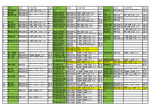
CSOT-华星光电 CONNECTOR FOR LCD 选型规格表
维安-芯导-韦尔手机用TVS对照表
11 12 13 14
WS07D3HP WS07DP WS07P4N WS12D3HP
SOD-323
485PF,2500W,0805 单向 3k/R
DFN1610-2L 400PF,1600W,0603 单向 3k/R DFN2020-2L 1000PF,6000W,2020 单向 3k/R SOD-323 265PF,1600W,0805 单向 3k/R
ESD5311N 22PF,100W,0402,单向 10k/R N/A 15PF,80W,0402,双向 10k/R ESD5471X 12PF,0402,双向 40k/R ESD5451R 10PF,80W,0402,双向 8k/R ESD5451X 15PF,12V,100W,0402 单向 8k/R N/A 8PF,90W,0402,双向 10k/R ESD9N12BA 2PF,80W,0402,单向 10k/R ESD5341N ESD9X5VL 3PF,80W,0402 双向 10k/R ESD9B5VL SOD923,3.5PF,80W,0402 双向 8k/R 0.5PF,100W,0402,单向 10k/R ESD9X5VU 0.5PF,100W,0402,单向 8k/R ESD5301N 0.3PF,100W,0402,双向 10k/R N/A 0.3PF,100W,0402,双向 8k/R 7V,150PF,400W,0603,单向 3k/R 0402,7V 单向 0402,7V 双向 260PF,2400W,0805,双向 3k/R ESD5621W04 600PF,7000W,双向 260PF,2400W,0603,双向 300PF,2700W,双向 3k/R ESD56131W 80PF,500W,0402,双向 10k/R ESD5651N 500PF,1100W,0805,单向 3k/R ESD5601W 640PF,2000W,0805,单向 3k/R 7V,1400W ESD5661D07 1700PF,7500W,2020,单向 3k/R ESD5641D07 73PF,230W,0402,单向 10k/R ESD5681N07 295PF,1300W,0805,单向 3k/R ESD5621W 395PF,2000W,0805,单向 3k/R 100PF,500W,0805,单向 3k/R 12V,1600W ESD5661D12 1000PF,9000W,2020,单向 3/R ESD5641D12 46PF,180W,0402,单向 10k/R ESD5681N12 520PF,3700W,双向 3k/R N/A 480PF,2200W,双向 3k/R 200W,单向 3k/R 350PF,3200W,双向 3k/R N/A 450PF,5000W,双向 3k/R 200W,单向 3k/R
华星光电第二条11代线确定8K大屏和OLED是方向
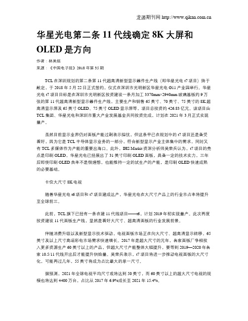
华星光电第二条11代线确定8K大屏和OLED是方向作者:林美炳来源:《中国电子报》2018年第35期TCL在深圳规划的第二条第11代超高清新型显示器件生产线(即华星光电t7项目)终于敲定,于2018年5月22日正式签约,仪式在深圳市光明新区华星光电G11产业园举行。
华星光电t7项目目标是在深圳市光明新区投资建设一条月加工3370mm×2940mm玻璃基板约9万张的第11代超高清新型显示器件生产线,主要生产和销售65英寸、70英寸、75英寸的8K超高清显示屏及65英寸OLED、75英寸OLED显示屏等,项目总投资约426.83亿元。
该项目由TCL集团、华星光电和深圳市重大产业发展基金共同投资完成,计划在2021年3月正式实现量产。
虽然目前显示业界仍对面板产能过剩表示担忧,但这条早已在规划中的t7项目还是备受看好,因为它是TCL半导体显示业务的一部分,符合新型显示产业主体集中的需求,同时又有TCL多媒体作为产能的重要出海口。
此外,IHS Markit资深分析师吴荣兵认为,t7项目的亮点是印刷OLED,华星光电已经展出了31英寸印刷OLED面板,具备一定的技术实力,三年后即使印刷OLED良率不是很理想,也能维持一定的试生产的产能,是印刷OLED快速成熟的必要基础。
卡位大尺寸8K电视随着华星光电t6项目和t7项目建成达产,华星光电在大尺寸产品上的行业市占率将提升至全球前三。
此前,TCL旗下已经有一条在建11代线项目——t6,计划2019年初实现量产。
此次再度投资建设11代面板生产线,显然是看好大尺寸、超高清面板的行业发展前景。
伴随消费升级以及新型显示技术驱动,电视面板市场正在向大尺寸、超高清显示转移,65英寸及以上尺寸高端彩电市场需求快速增长。
2017年是超大尺寸的元年,各家面板厂争相投入更多资源生产60英寸以上的产品,但超大尺寸产能整体大幅提升,要等到2019—2020年各家10.5/11代线开出后才能提升供给量。
1.8寸LCD模块用户手册说明书
1.8inch LCD ModuleUSER MANUALOVERVIEWThis product is 1.8inch resistive screen module with resolution 128x160. It has internal controller and uses SPI interface for communication. It has already basic functions: setting the point size, the line thickness, drawing circle, rectangle, and displaying English characters.We provide Raspberry Pi, STM32 and Arduino routines for this product.FEATURESDisplay type: TFTInterface: SPIDriver: ST7735SColors: 256KResolution: 128 x 160 (Pixel)Product size: 56.5 x 34(mm)Display size: 35.4(W) x 28.03(H)(mm)Pixel size: 0.219(W) x 0.219(H)(MM)Operating temperature: -30°C ~ 85°CINTERFACE DESCRIPTIONMarking Description3V3 3.3V powerGND groundDIN SPI data inputCLK SPI clockCS chip selectDC data/commandRST resetBL back lightPROGRAM ANALYSIS1.Working principles:ST7735S is 132 x 162 pixels LCD panel, but the product is 128 x 160 pixels LCD display.In the display there are two processes: the horizontal direction scanning – from the 2nd pixel, the vertical direction scanning – from the 1st pixel. So, you can see that positions of pixels in RAM correspond to their actual positions while displaying.The LCD supports 12-bit, 16-bit and 18-bit per pixel input formats. They correspond to RGB444, RGB565 and RGB666 color formats. This routine uses the RGB565 color format, which is commonly used.LCD uses 4-wired SPI communication interface, which can save a lot of GPIO ports and provides fast data transfer to LCD as well.munication protocolNote: there is a difference from traditional SPI. Here we only need display, so sine wires come from slave to host are hidden. The detailed information please refer to datasheet at page 58RESX: Reset. Pull-down while powering on the module. Generally set as 1IM2: data communication mode pin, which define usage of SPICSX: chip selection control pin. If CS=0 – the chip is selectedD/CX: data/command control pin, if DC=0 – command is written, otherwise – data are writtenSDA: transmitted RGB dataSCL: SPI clockThe SPI communication protocol of the data transmission uses control bits: clock phase (CPHA) and clock polarity (CPOL):The value of CPOL determines the level when the serial synchronous clock is in idle state. CPOL=0, that its idle level is 0.The value of CPHA determines the timing of the data bits relative to the clock pulses. CPHA=0, data is sampled at the first clock pulse edge.The combination of these two parameters provides 4 modes of SPI data transmission. The commonly used is SPI0 mode, it is that GPOL=0 and CPHA=0.From the figure above, SCLK begins to transfer data at the first falling edge. 8 bits data are transferred at one clock period. Use SPI0 mode, High bits transfer first, and LOW bits following. DEMO CODERaspberry Pi, STM32 and Arduino programs are provided, wherein Raspberry Pi provides BCM2835, WiringPi and python programs. It implements common graphical functions as drawing dot, line, rectangle, circle, setting their sizes and line with; filling arias, and displaying English characters of 5 common fonts and other display’s functions.Following instructions are offered for you convenienceRASPBERRY1.Hardware connection1.8inch LCD module Raspberry Pi3.3V 3.3VGND GNDDIN MOSI (PIN 19)CLK SCLK (PIN23)CS CE0 (PIN 8)DC GPIO.6 (PIN 22)RST GPIO.2 (PIN13)BL GPIO.5 (PIN18)2.Enable SPI function of the Raspberry Pisudo raspi-configSelect: Advanced Options -> SPI -> yesActivate SPI hardware driver.3.Installation of librariesFore detailed information about libraries installation, please refer to this page:https:///wiki/Libraries_Installation_for_RPiIt is description of WiringPi, bcm2835 and python libraries installation.ageBCM2835 and WiringPi program should be only copied into directory of Raspberry Pi ()by samba or directly copy to the SD card). The following code are compied directly to the user directory of Pi.4.1Usage of BCM2835Run ls command as you can see below:bin: contains “.o” files.We don’t need to change it generallyFonts: contains 5 commonly used fontsPic: contains pictures used for displaying. The resolution of pictures must be 128x128,otherwise they cannot be displayed properly. And the format of pictures must be BMP.Obj: contains object files, like main.c, LCD_Driver.c, DEV_Config.c, LCD_GUI.c and theirheader files.main.c: The mian function. What need to note is that even though there are LCD_ScanDir used to control the direction of scanning, you need not to change it. Because this module is designed for Raspberry Pi, and for compatibility, we don’t recommend you to change it.DEV_Config.c:Definations of Raspberry Pi’s pins and the communication mode.LCD_Driver.c: Drive code of LCD. Need not change generally.LCD_BMP.c: Reading and analyzing BMP files and display themMakefile: This file contains compilation rules. If there are some changes in code, please run make clean to clean all the dependency file and executable files. Then execute make to compile the whole project and generate new executable files.tftlcd_1in8: executable file, generated by command makeTo run the program, you just need to run this command on terminal: sudo ./tftlcd_1in8 4.2WiringPiInput ls command, now you can see following:T he folders is similar to BCM2835’s. The only differences are that:1.WiringPi oprates by read/write the device files of Linux OS. and the bcm2835 is libraryfunction of Raspberry Pi’s CPU, it operates registers directly. Thus, if you have usedbcm2835 libraries firstly, the usage of WiringPi code will be failed. In this case, you just need to reboot the system and try again.2.Due to the first difference, they underlying configuration are different. In DEV_Config.c,use wiringpiPi and the corresponding wiringPiSPI to provide underlay interfaces.The program executed by command sudo ./tftlcd_1in8 as well4.3PythonInput ls command, you can see that:LCD_1in8.py: Driver code of LCDLCD_Config.py: configuration of hardware underlaying interface.Executing program: sudo python LCD_1in8.pyNote: Some of the OS don’t have image libraries. In this case, you can run: sudo apt-get install python-imaging to install the image library.Image is an image processing library of python, represents any image by an image object.Thus, we can create a blank image by new, its size must be same as the display size of LCD.Then draw picture by Draw library, finally, transfer the image to the LCD. Here usingImage.load() too read RGB888 data of pixel, and convert to RGB565. Scanning every pixel then we could get the whole image for displaying. Its most important code is as below:5.Auto-runInitialize autorun in Raspberry Pi by configuring code of /etc/rc.local file:sudo vim /etc/rc.localBefore exit0 add:sudo python /home/pi/python/demo.py &Important: to place the program /home/pi/python/demo.py at the same director, you can input command pwd to get the path. And & character is necessary at the end of command line, otherwise probable need to reinstall the system (impossible terminate the process by pressing ctrl+c, impossible to login with pi user permission).STM32This demo uses XNUCLEO-F103RB developing board and is based on HAT library.1.Hardware connection1.8inch LCD XNUCLEO-F103RBVCC 3V3GND GNDDIN PA7CLK PA5CS PB6DC PA8RST PA9BL PC72.Expected resultProgram the demo into the development Board. Firstly the screen is refreshed completely, then a solid line, dashed line, open circle, solid circle, rectangle, solid torque are drawn and English characters are shown.ARDUINOUNO PLUS Arduino development board is used here.1.Hardware connection1.8inch LCD Arduino3.3V 3V3GND GNDDIN D11CLK D13CS D10DC D7RST D8BL D92.Due to small global memory 2Kb of UNO PLUS, the display can’t work in graphical mode,but the calling method is the same. Just because there is no enough memory, this demo is not provided.COMPATIBLE CODE PORTINGOffered demo is the commonly used programs, which are able to be ported. They can be used with two screens and the difference is only in initialization of them and their sizes.The usage method is defined by macros. In LCD_Driver.h or in LCD.h:#define LCD_1IN44#define LCD_1in8.As the name of the macros, they are used for 1.44inch and 1.8inch LCD separately. To use for one LCD, just need to comment other one.For example://#define LCD_1IN44#define LCD_1IN8Here we use it for 1.8inch LCD, so we comment the 1.44 macro. After saving, Run make clean to remove dependency files, and then run make to generate new executable files.。
华星光电tft-lcd液晶面板3d技术及fpd(g4.5代)研发线项目申请立项环境影响评估报告书
TFT-LCD液晶面板3D技术及FPD(G4.5代)研发线项目环境影响报告书(简本)建设单位:深圳市华星光电技术有限公司编制单位:深圳市环境科学研究院二〇一二年十二月目录第一章总论 (1)1.1 前言 (1)1.2 区域环境功能属性 (2)1.3 评价工作等级 (2)1.4 评价工作范围 (3)1.5 环境敏感点及环境保护目标 (3)第二章工程概况 (5)2.1 项目基本情况 (5)2.2项目地理位置和四至情况 (5)2.3 劳动定员及工作制度 (5)2.4 项目进度安排 (6)第三章工程分析 (7)3.1 工艺流程及产污环节分析 (7)3.2 水平衡 (7)3.3 污染源强及排放情况 (8)第四章环境质量现状调查与评价 (11)4.1 地表水环境质量现状 (11)4.2 地下水环境质量现状 (11)4.3 环境空气 (11)4.4 土壤环境质量现状 (11)4.5 声环境质量现状 (11)第五章环境影响预测与评价 (13)5.1 地表水环境影响评价 (13)5.2 地下水环境影响评价 (13)5.3 环境空气影响评价 (13)5.4 声环境影响评价 (14)5.5 固体废物环境影响评价 (15)5.6 环境风险评价 (15)第六章环境保护措施及可行性论证 (17)6.1 环境保护措施技术可行性分析 (17)6.2 环保投资估算 (19)第七章清洁生产和总量控制 (21)7.1 清洁生产评价 (21)7.2 总量控制 (21)第八章环境管理与环境监测 (23)8.1 环境管理 (23)8.2 环境监测 (23)第九章环境影响经济损益分析 (25)第十章产业政策、规划符合性及选址合理性分析 (27)10.1 产业政策及规划相符性分析 (27)10.2 项目选址与总图合理性 (27)第十一章公众参与 (29)第十二章综合结论 (31)第一章总论1.1 前言深圳市华星光电技术有限公司(以下简称“华星光电”)于2009年成立于深圳市光明新区高新技术产业园区,主要从事薄膜晶体管液晶显示器件(以下简称“TFT-LCD”)的开发、制造、销售以及售后服务。
液晶8脚贴片元器件参数大集合
液晶8脚贴片元器件参数大集合4532 内含P沟道、N沟道MOS管各一,高压板用(30V 4.7A;30V 4.5A)4532M 内含P沟道、N沟道MOS管各一,高压板用(30V 4.5A;30V 4.5A)9916H 18V 35A 50W 小贴片9960GM 8脚贴片,高压板用。
AF4502CS 内含P沟道、N沟道MOS管各一,高压板用(30V 8.4A;30V 6.8A) AO4403 30V 6.1A 单P沟道 8脚贴片AO4404 30V 8.5A 单N沟道 8脚贴片AO4405 30V 6A 3W 单P沟道8脚贴片AO4406 30V,11.5A,单N沟道,8脚贴片AO4407 30V 12A 3W 单P沟道,8脚贴片AO4407 30V 12A 3W 单P沟道,8脚贴片AO4408 30V 12A 单N沟道 8脚贴片AO4409(30V15A-P) 30V 15A P沟道场效应 8脚贴片AO4410 30V 18A 单N沟道 8脚贴片AO4411 30V 8A 3W P沟道场效应,8脚贴片AO4413 30V 15A 3W 单P沟道,8脚贴片AO4413 30V 15A 3W 单P沟道,8脚贴片AO4414 30V,8.5A,3W 单N沟道,8脚贴片AO4418 30V 11.5A N沟道 8脚贴片AO4422 30V 11A N沟道 8脚贴片AO4423 30V 15A 3.1W 单P沟道,8脚贴片AO4425 38V 14A P沟道8脚贴片AO4431 30V,8A P沟道。
高压板用MOS,贴片8脚AO4600 内含P沟道、N沟道MOS管各一,高压板用(30V 6.9A;30V 5A)AO4606 内含P沟道、N沟道MOS管各一,高压板用(30V 6.9A;30V 6A)AO4607 内含P沟道、N沟道MOS管各一,高压板用AO4828 60V 4.5A 双N沟道 8脚贴片AOD405 30V,18A,P 高压板MOS管贴片AOD408 30V,18A,N 高压板MOS管贴片AOD409 60V 26/18A P 高压板MOS管贴片AOD409 60V 26/18A P 高压板MOS管贴片AOD420 30V,10A,N 高压板MOS管贴片AOD442 60V,38/27A,N 高压板MOS管贴片AOD442 60V,38/27A,N 高压板MOS管贴片AOD444 60V,12A,N 高压板MOS管贴片AOP600 内含P、N沟道各1,30V 7.5A、30V 4.5A。
AUO_G173HW01_v0_20110530

() Preliminary Specification(V) Final SpecificationModule 17.3” FHD Color TFT-LCD Model Name G173HW01 V0Customer Date Approved byNote: This Specification is subject to change without notice.Checked &Approved by DateVito Huang2011/5/30 Prepared byVivian Huang2011/5/30Audio Video Business Group /AU Optronics corporationContents1. Handling Precautions (4)2. General Description (5)2.1 Display Characteristics (5)3. Functional Block Diagram (10)4. Absolute Maximum Ratings (11)4.1 Absolute Ratings of TFT LCD Module (11)4.2 Absolute Ratings of Environment (11)5. Electrical characteristics (12)5.1 TFT LCD Module (12)5.2 Backlight Unit (14)6. Signal Characteristic (15)6.1 Pixel Format Image (15)6.2 The Input Data Format (16)6.4 Interface Timing (19)6.5 Power ON/OFF Sequence (20)7. Connector & Pin Assignment (21)7.1 TFT LCD Module (21)7.2 Backlight Unit (22)8. Reliability Test (23)9. Shipping Label (24)10. Packing Form (25)10.1 Packaging material (25)10.2 External packaging material required (25)10.3 Palletizing sequence (26)10.4 Packing instruction (27)11. Outline Drawing (28)Record of RevisionVersion & Date PageOld DescriptionNew Description0.0 2011/1/20 All First Edition for Customer0.1 2011/1/31 12 IDD unit: A IDD unit: mA 14 VCC Max: 12.6V VCC Max: 13.4V14 Operation LifeLED life time1.0 2011/5/30 5 White Luminance(cd/m 2): 500(Typ.) White Luminance(cd/m 2): 400(Typ.) 5 Optical Response Time(ms): 8(Typ.)Optical Response Time(ms): 40(Typ.)5 Power Consumption(Watt): TBD(Typ.) Power Consumption(Watt): 17(Typ.) 5 Weight(g): TBD(Typ.) Weight(g): 1080(Typ.)6 Update Viewing Angle 6 Update Optical Response Time6 Update Color / Chromaticity Coordinates6Update White Luminance 12 IDD (mA): 350(Typ), 600(Max) IDD (mA): 1200(Typ), 1400(Max) 12 PDD (Watt): TBD(Typ), 2(Max) PDD (Watt): 5(Typ), 6(Max)12Update the diagram of Vin rising time 14 P VCC (Watt): 11.88(Typ), 13.39(Max) P VCC (Watt): 12(Typ), 15(Max) 14 Update LED Forward Voltage 14 Update Note6 description 25 Update Shipping Label25 Update Packing Form28Update Outline Drawing1. Handling Precautions1) Since front polarizer is easily damaged, please be cautious and not to scratch it.2) Be sure to turn off power supply when inserting or disconnecting from input connector.3) Wipe off water drop immediately. Long contact with water may cause discoloration or spots.4) When the panel surface is soiled, wipe it with absorbent cotton or soft cloth.5) Since the panel is made of glass, it may be broken or cracked if dropped or bumped on hard surface.6) To avoid ESD (Electro Static Discharde) damage, be sure to ground yourself before handling TFT-LCD Module.7) Do not open nor modify the module assembly.8) Do not press the reflector sheet at the back of the module to any direction.9) In case if a module has to be put back into the packing container slot after it was taken out from the container, do not press the center of the LED light bar edge. Instead, pressat the far ends of the LED light bar edge softly. Otherwise the TFT Module may be damaged.10) At the insertion or removal of the Signal Interface Connector, be sure not to rotate nor tilt the Interface Connector of the TFT Module.11) TFT-LCD Module is not allowed to be twisted & bent even force is added on module in a very short time. Please design your display product well to avoid external force applying to module by end-user directly.12) Small amount of materials without flammability grade are used in the TFT-LCD module. The TFT-LCD module should be supplied by power complied with requirements of Limited Power Source (IEC60950 or UL1950), or be applied exemption.13) Severe temperature condition may result in different luminance, response time and lamp ignition voltage.14) Continuous operating TFT-LCD display under low temperature environment may accelerate lamp exhaustion and reduce luminance dramatically.15) The data on this specification sheet is applicable when LCD module is placed in landscape position.16) Continuous displaying fixed pattern may induce image sticking. It’s recommended to use screen saver or shuffle content periodically if fixed pattern is displayed on the screen.2. General DescriptionG173HW01 V0 is a Color Active Matrix Liquid Crystal Display composed of a TFT-LCD panel, a LED driver circuit, and a LED backlight system. The screen format is intended to support the FHD (1920(H) x 1080(V)) screen and 16.7M colors (RGB 6-bits + HiFRC data). All input signals are LVDS interface compatible. Inverter card of backlight is not included.2.1 Display CharacteristicsThe following items are characteristics summary on the table under 25 ℃condition:Items Unit Specifications Screen Diagonal [mm] 17.3W (17.25)Active Area [mm] 381.888 (H) x 214.812 (V)Pixels H x V 1920(x3) x 1080Pixel Pitch [mm] 0.1989 (per one triad) x 0.1989Pixel Arrangement R.G.B. Vertical StripeDisplay Mode Normally WhiteWhite Luminance [cd/m2] 400 (Typ.)Contrast Ratio 600 : 1 (Typ)Optical ResponseTime [msec] 40 (Typ, on/off)Nominal Input Voltage VDD [Volt] 3.3 VPower Consumption [Watt] 17 (Typ)Weight [Grams] 1080 (Typ)Physical Size (H x V x D) [mm] 403 (H) x 240 (V) x 12.5 (D) (Typ) Electrical Interface Dual channel LVDSSurface Treatment Hard-coating (3H), Glare treatment Support Color 16.7M colors (RGB 6-bit data + HiFRC data)Temperature Range (Ta) Operating Storage (Non-Operating) [o C][o C]0 to +70-20 to +70RoHS Compliance RoHS Compliance2.2 Optical CharacteristicsThe optical characteristics are measured under stable conditions at 25℃ (Room Temperature):ItemUnit Conditions Min.Typ.Max.NoteHorizontal (Right) CR = 10 (Left) 70 70 80 80 -Viewing Angle [degree]Vertical (Up) CR = 10 (Down) 50 70 60 80 - 1Luminance Uniformity [%] 13 Points 75 80 - 2, 3Rising - 37 50 Falling - 3 10 Optical Response Time[msec] Rising + Falling -4060 4, 5 Red x 0.590 0.640 0.690 Red y 0.296 0.346 0.396 Green x 0.264 0.314 0.364 Green y 0.574 0.624 0.674 Blue x 0.100 0.150 0.200 Blue y 0.004 0.054 0.104 White x 0.255 0.305 0.355 Color / Chromaticity Coordinates (CIE 1931)White y0.268 0.318 0.368 4 White Luminance (At LED=100mA) [cd/m2 ]320 400 - 4 Contrast Ratio 500 600 - 4 NTSC%72Optical Equipment: BM-5A, BM-7, PR880, or equivalentNote 1: Definition of viewing angleViewing angle is the measurement of contrast ratio≧10, or ≧5, at the screen center, over a 180° horizontal and 180° vertical range (off-normal viewing angles). The 180° viewing angle range is broken down as follows; 90° (θ) horizontal left and right and 90° (Φ) vertical, high (up) and low (down). The measurement direction is typically perpendicular to the display surface with the screen rotated about its center to develop the desired measurement viewing angle.Note 2: 13 points positionNote 3:Note 4: Measurement methodThe LCD module should be stabilized at given temperature for 30 minutes to avoid abrupt temperature change during measuring. In order to stabilize the luminance, the measurement should be executed after lighting Backlight for 30 minutes in a stable, windless and dark room.Note 5: Definition of response time:The output signals of photo detector are measured when the input signals are changed from “Full Black” to “Full White” (rising time), and from “Full White” to “Full Black” (falling time), respectively. The response time is interval between the 10% and 90% of amplitudes. Please refer to the figure as below.3. Functional Block DiagramThe following diagram shows the functional block of the 17.3 inches Color TFT-LCD Module:4. Absolute Maximum RatingsAbsolute maximum ratings of the module are as following:4.1 Absolute Ratings of TFT LCD ModuleItem Symbol Min Max Unit Logic/LCD Drive Voltage Vin -0.3 +3.6 [Volt]4.2 Absolute Ratings of EnvironmentItem Symbol Min Max Unit Operating Temperature TOP 0 +70 [o C] Operation Humidity HOP 5 95 [%RH] Storage Temperature TST -20 +70 [o C] Storage Humidity HST 5 95 [%RH] Note: Maximum Wet- and no condensation.5. Electrical characteristics 5.1 TFT LCD Module5.1.1 Power Specification Input power specifications are as follows:SymbleParameter Min.Typ.Max.UnitConditionVDD Logic/LCD DriveVoltage 3.0 3.3 3.6 [Volt] ±10%IDD Input Current - 1200 1400 [mA] VDD= 5.0V, All Black Pattern At 75Hz, +30%PDD VDD Power - 5 6 [Watt] VDD= 5.0V, All Black Pattern At 75Hz , Note 1IRush Inrush Current- - 2000 [A] Note 2VDDrpAllowable Logic/LCD Drive Ripple Voltage --100[mV] p-pVDD= 3.3V, All Black Pattern At 75HzNote 1: The variance of VDD power consumption is ±30%. Note 2: Measurement conditions:Vin rising time0V5.1.2 Signal Electrical Characteristics Input signals shall be low or Hi-Z state when VDD is off. Note: LVDS Signal Waveform.5.2 Backlight UnitFollowing characteristics are measured under a stable condition using a inverter at 25℃. (Room Temperature): Symbol Parameter Min.Typ.Max.Unit RemarkVCC Input Voltage 10.8 12 13.4 [Volt]I VCC Input Current - 0.99 - [A] 100% PWM DutyP VCC Power Consumption - 12 15 [Watt]100% PWM DutyF PWM Dimming Frequency 200 - 20K [Hz]Swing Voltage 3 3.3 5.5 [Volt]Dimming duty cycle 5 - 100 %I F LED Forward Current-100 -[mA] Ta = 25o C- (3.3) (3.7) [Volt]I F = 100mA, Ta = 0o C- 3.2 3.6 [Volt]I F = 100mA, Ta = 25o C V F LED Forward Voltage- (3.1) (3.5) [Volt]I F = 100mA, Ta = 70o C P LED LED Power Consumption- (10.24)11.52 [Watt]LED Life Time50,000 - - Hrs I F=100mA, Ta= 25o CNote 1: Ta means ambient temperature of TFT-LCD module.Note 2: VCC, I VCC, P VCC are defined for LED backlight.(100% duty of PWM dimming)Note 3: I F, V F are defined for one channel LED. There are four LED channel in back light unit.Note 4: If G173HW01 V0 module is driven by high current or at high ambient temperature & humidity condition. The operating life will be reduced.Note 5: Operating life means brightness goes down to 50% initial brightness. Minimum operating life time is estimated data.Note 6: LED lifetime is definition: brightness is decreased to 50% of the initial value. LED lifetime is restricted under6. Signal Characteristic6.1 Pixel Format ImageFollowing figure shows the relationship of the input signals and LCD pixel format.1st2nd1919th1920th1stLine1080thLin6.2 The Input Data FormatNote1: Normally, DE, VS, HS on EVEN channel are not used. Note2: 8-bit in6.3 Signal DescriptionThe module using a pair of LVDS receiver SN75LVDS82(Texas Instruments) or compatible. LVDS is a differential signal technology for LCD interface and high speed data transfer device. Transmitter shall be SN75LVDS83(negative edge sampling) or compatible. The first LVDS port(RxOxxx) transmits odd pixels while the second LVDS port(RxExxx) transmits even pixels.PIN #SIGNAL NAME DESCRIPTION1 RxOIN0- Negative LVDS differential data input (Odd data)2 RxOIN0+ Positive LVDS differential data input (Odd data)3 RxOIN1- Negative LVDS differential data input (Odd data)4 RxOIN1+ Positive LVDS differential data input (Odd data)5 RxOIN2- Negative LVDS differential data input (Odd data, H-Sync,V-Sync,DSPTMG)6 RxOIN2+ Positive LVDS differential data input (Odd data, H-Sync,V-Sync,DSPTMG)7 VSS Power Ground8 RxOCLKIN- Negative LVDS differential clock input (Odd clock)9 RxOCLKIN+Positive LVDS differential clock input (Odd clock)10 RxOIN3- Negative LVDS differential data input (Odd data)11 RxOIN3+ Positive LVDS differential data input (Odd data)12 RxEIN0- Negative LVDS differential data input (Even data)13 RxEIN0+ Positive LVDS differential data input (Even data)14 VSS Power Ground15 RxEIN1- Negative LVDS differential data input (Even data)16 RxEIN1+ Positive LVDS differential data input (Even data)17 VSS Power Ground18 RxEIN2- Negative LVDS differential data input (Even data)19 RxEIN2+ Positive LVDS differential data input (Even data)20 RxECLKIN- Negative LVDS differential clock input (Even clock)21 RxECLKIN+ Positive LVDS differential clock input (Even clock)22 RxEIN3- Negative LVDS differential data input (Even data)23 RxEIN3+ Positive LVDS differential data input (Even data)24 VSS Power Ground25 VSS Power Ground26 VSS Power Ground27 VSS Power Ground28 VDD +3.3V Power Supply29 VDD +3.3V Power Supply30 VDD +3.3V Power SupplyNote1: Start from left sideRxOIN0-VDDNote2: Input signals of odd and even clock shall be the same timing. Note3: Please follow PSWG.6.4 Interface Timing6.4.1 Timing CharacteristicsBasically, interface timings should match the 1920X1080 / 60Hz manufacturing guide line timing.Note : DE mode only6.4.2 Timing Diagram6.5 Power ON/OFF SequenceVDD power and lamp on/off sequence is as follows. Interface signals are also shown in the chart. Signals from any system shall be Hi-Z state or low level when VDD is off.Power Sequence TimingPower Sequence TimingValueUnitsParameterMin. Typ. Max.T1 0.5 - 10T2 0 - 50T3 200 - --T4 0.5 - 10T5 10 - -T6 10 - -msT7 0 - -T8 10 - -T9 - - 10T10 110 - -T11 0 50T12 0 10T13 500 - -7. Connector & Pin AssignmentPhysical interface is described as for the connector on module.These connectors are capable of accommodating the following signals and will be following components.7.1 TFT LCD Module7.1.1 ConnectorConnector Name / Designation Interface Connector / Interface card Manufacturer HRSType Part Number MDF76TW-30S-1HMating Type Part Number MDF76-30P-1C7.1.2 Pin AssignmentPin#Signal Name Pin#Signal Name1 RxOIN0-2 RxOIN0+3 RxOIN1-4 RxOIN1+5 RxOIN2-6 RxOIN2+7 VSS 8 RxOCLKIN-9 RxOCLKIN+ 10 RxOIN3-11 RxOIN3+ 12 RxEIN0-13 RxEIN0+ 14 VSS15 RxEIN1- 16 RxEIN1+17 VSS 18 RxEIN2-19 RxEIN2+ 20 RxECLKIN-21 RxECLKIN+ 22 RxEIN3-23 RxEIN3+ 24 VSS25 VSS 26 VSS27 VSS 28 VDD29 VDD 30 VDD7.2 Backlight UnitPhysical interface is described as for the connector on module. These connectors are capable of accommodating the following signals and will be following components.7.2.1 ConnectorConnector Name / Designation Lamp Connector / Backlight lamp Manufacturer HRSType Part Number DF14A-6P-1.25HMating Type Part Number DF14-6S-1.25C7.2.2 Pin AssignmentPin No. Symbol DescriptionPin1 VLED 12V inputPin2 VLED 12V inputPin3 GND GNDPin4 GND GNDPin5 On/OFF 3.3-5V:ON, 0V:OFFPin6 Dimming PWM8. Reliability TestEnvironment test conditions are listed as following table.Items Required Condition Note Temperature Humidity Bias (THB) Ta= 50℃, 80%RH, 240hoursHigh Temperature Operation (HTO)Ta= 70℃, 240hoursLow Temperature Operation (LTO) Ta= 0℃, 240hoursHigh Temperature Storage (HTS) Ta= 70℃, 240hoursLow Temperature Storage (LTS) Ta= -20℃, 240hoursVibration Test (Non-operation) Acceleration: 1.5 GWave: Random Frequency: 10 - 200 - 10 Hz Sweep: 30 Minutes each Axis (X, Y, Z)Shock Test (Non-operation) Acceleration: 50 GWave: Half-sineActive Time: 20 msDirection: ±X,±Y,±Z (one time for each Axis)Drop Test Height: 60 cm, package testThermal Shock Test (TST) -20℃/30min, 60℃/30min, 50 cycles 1Contact Discharge: ± 8KV, 150pF(330Ω ) 1sec,8 points, 25 times/ point.ESD (Electro-Static Discharge)Air Discharge: ± 15KV, 150pF(330Ω ) 1sec8 points, 25 times/ point.2Note 1: The TFT-LCD module will not sustain damage after being subjected to 100 cycles of rapid temperature change. A cycle of rapid temperature change consists of varying the temperature from -20℃to 60℃, and back again. Power is not applied during the test. After temperature cycling, the unit is placed in normal room ambient for at least 4 hours before power on.Note 2: According to EN61000-4-2, ESD class B: Some performance degradation allowed. No data lost.Self-recoverable. No hardware failures.9. Shipping LabelUnit: mm10. Packing Form10.1 Packaging materialFILM PROTECTBAG ANTI-STATICTAPETAPE CREPED PAPERPACKING CARTONLABEL SPECLABEL CARTON.CUSHION PACKING10.2 External packaging material required‧Carton : 524mm*321mm*360mm, weight (carton + cushion): 1250g‧Pallet : 1140mm*980mm*140mm‧Stretch film : 500mm (W)*300M (L)‧Corner angle : L type fiber board‧PET band : 19mm (W)‧ Label : 220mm*200mm10.3 Palletizing sequencepcs / box box / layer layer / pallet pcs / pallet Shipping by air 10 2*3 3 180 Shipping by sea 10 2*3 3 180A U O P T R O N I C S C O R P O R A T I O NP r o d u c t S p e c i f i c a t i o nm e n t v e r s i o n 1.0 27/29G 173H W 01 V 0P a c k i n g i n s t r u c t i o nA U O P T R O N I C S C O R P O R A T I O NP r o d u c t S p e c i f i c a t i o nm e n t v e r s i o n 1.0 28/29G 173H W 01 V 0A U O P T R O N I C S C O R P O R A T I O NP r o d u c t S p e c i f i c a t i o nm e n t v e r s i o n 1.0 29/29G 173H W 01 V 0。
智能手机液晶显示模组基础知识
480x800
JD9161/ILI9806E/7701S/ GC9503V
MIPI Vedio
480x854
JD9161/ILI9806E/7701S/ 9503V
MIPI Vedio
2.0" QCIF 176x220 ST7775R/NV3038B/GC9203
2.2" QCIF 176x220 ST7775R/NV3038B/GC9203
ST7796S/ILI9488
MIPI、 MCU16
1.54" QVGA
240x240
7789H2/7789V2/GC9305/GC 9306/ NV3029G-01
1.77" QQVGA 128x160
ST7735S/GC9106 NV3021C-01/NV3021BW
3.97" WVGA SPI4、 MCU8
框贴与全贴合对比效果图
4.3 OGS简介
OGS技术英文全称是 ONE GLASS SOLUTION, 即单片触摸屏幕,是为了与多片 (比如G+G,G+F,G+FF等)进行区别,原来的触摸屏需要多片玻璃或者膜片, 而OGS是将触摸 sensor直接做到玻璃盖板上的技术,这样比多片可以薄很多, 而且显示效果更好,更清晰。OGS技术:由OGS层粘合LCD层,共2层。
东莞市龙芯光电有限公司
智能手机液晶显示模组基础知识
编制:黄忠乐
目录
1. 显示屏技术参数 2.显示屏产品类型 3.电容触摸屏产品类型及物料选材 4.贴合技术介绍
1. 显示屏技术参数 1.1 屏幕尺寸
1.2 分辨率
分辨率:显示分辨率(屏幕分辨
中国内地主要液晶面板工厂生产线分布及其供应链汇总

中国内地主要液晶⾯板⼯⼚⽣产线分布及其供应链汇总在中国进⼝的⼯业产品中,显⽰⾯板的⾦额长期处于第三位,第⼀位是半导体,第⼆位是汽车整车和零部件,第三位就是显⽰⾯板。
2016年全球智能⼿机⾯板出货量达21.1亿⽚,相⽐2015年增长达16.4%超出预期。
前三甲分别为三星(17.6%)、京东⽅(17.1%)、LGD(10.0%)。
依照⾯板供应商所在地统计,中国地区⾯板供应商出货同⽐⼤幅增加44.5%,主要为a-Si产品及LTPS⾯板产出上的增加。
⽽韩国地区因韩国三星AMOLED的出货⼤幅成长,该地区出货同⽐增长22.1%,⽇本地区和台湾地区则分别同⽐下降12.3%和0.6%。
No.1 三星显⽰器 Samsung Display韩过三星以3.7亿⽚AMOLED⾯板出货跃居全球第⼀⼤智能机⾯板供应商,同⽐增幅39.6%,市场占有率17.6%,使得AMOLED⼿机屏在智能机⾯板中的全球市场份额由2015年的14.7%提升⾄17.8%。
No.2 京东⽅科技集团 BOE国内⾯板企业京东⽅以3.6亿⽚位居第⼆,同⽐增长16.1%,市场份额17.1%。
其中,京东⽅LTPS⾯板出货超4000万⽚,同⽐增长320%。
如不计算AMOLED⾯板市场,京东⽅仍以17.8%的市占率为智能⼿机液晶屏市场最⼤⾯板供应商。
No.3 乐⾦显⽰器 LG Display韩国LGD以2.1亿⽚位居第三,与第⼆名京东⽅差距1.5亿⽚,市场份额10.0%。
LGD关闭多座G5以下产线,使得其出货量与2015年持平。
LGD 2016年发⼒⼿机柔性AMOLED显⽰屏,成功打⼊⼩⽶,2017年柔性AMOLED出货量上看1000万部。
No.4 ⽇本显⽰器 JDI⽇本JDI以1.9亿⽚位居第四,市场份额9.0%,由于国内品牌在2016年⼤⼒转向AMOLED⾯板,且苹果iPhone系列销售不如预期,导致JDI在2016年智能机⾯板销量同⽐降低5.0%。
No.5 中华映管 CPT台湾CPT(含凌巨)以1.6亿⽚位居第五,市场份额7.5%。
32寸液晶电视参数对比
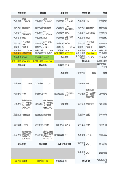
单屏尺寸 750*478*5 (宽*高* 4(最薄处 厚)mm 32mm)mm
含底座重量 (kg)
8.7kg
含底座尺寸 (宽*高* 厚)mm
750*508*2 22 mm
外包装尺寸 (宽*高* 厚)mm
825*560*1 48 mm
含底座重量 (kg)
8.7kg
含底座尺寸 (宽*高* 厚)mm
750*508*2 22 mm
920 162
*530
*
主体参数
主体参数
主体参数
主体参数
主体参数
LG
产品品牌
索尼 (SONY)
产品品牌
索尼 (SONY)
产品品牌
索尼 (SONY)
飞利浦 产品品牌 (PHILIPS
)
合资品牌
品牌类别 合资品牌
品牌类别 合资品牌
品牌类别 合资品牌
品牌类别 合资品牌
32LM3100
产品型号
KLV32EX330
USB支持图 JPEG 片格式 (.jpg)
含底座尺寸 (宽*高* 厚)mm
769×530× 262
USB支持视 DivX 频格式 HD,RMVB
USB支持视 频格式
音频参数
音频参数
单屏尺寸 (宽*高* 厚)mm
769×489× 55
AC3(Dolby
USB支持音 频格式
Digital),EA C3,AAC,M peg,MP3,P
0
端口参数
USB接口 有
USB接口 有
电源功率 (w)
55W
机身侧面接 口
USB*1
待机功率 (w)
0.5W
USB音视图参数
机身侧面接 口
中国新TFT LCD世代线投资和发展趋势

中国大陆新的TFT LCD世代线投资和发展趋势 为了扩大产能,中国厂商正积极建新厂并购买平面显示器(FPD)生产设备,而且这种趋势仍将继续。
2010年,中国厂商在平板显示器生产设备上的花费仅占全球的22%,但此后这一比例不断增长,预计到2014及2015年将超过70%。
根据DisplaySearch 最新的研究报告显示, 中国厂商的新投资聚焦于新建八代线。
在政府的支持下,中国面板厂商正积极扩大其八代线的规模。
三星和LG也同样在中国投资新建八代线。
如此下去,中国将很快威胁到韩国的八代线领导地位。
然而,随着智能移动设备市场(如智能手机和平板计算机等)的不断壮大,中国面板厂的投资也不局限于八代线。
他们也开始投资一些规模较小但工艺和产品技术较高(如LTPS--低温多晶硅技术、oxide TFT—金属氧化物薄膜晶体管、OLED—有机发光二极管)等的面板生产线。
同时,DisplaySearch 也观察到, 海外LCD面板厂也想利用中国特殊的政治和投资环境的优势以增加他们的投资额。
一些海外面板厂已经在中国建造了工厂,并将目标瞄准智能手持设备市场。
NPD DisplaySearch 目前预计在中国大陆2014年到2016年可能新增16座新的面板工厂投入生产。
不过有些已开始进入建厂与机台设备的规划, 有些则尚处于评估与计划阶段。
中国大陆新的TFT LCD世代线投资和发展趋势来源:NPD DisplaySearch平板显示器供需及资本支出季度报告NPD DisplaySearch针对各个新厂投资进行了分析:BOE (京东方)BOE正积极扩大自己的产能,它是中国目前发展最激进的面板厂商。
BOE成功地运用了中国各地政府提供的优惠政策来实现它的投资计划。
这就是为什么BOE作为一个北京公司,却能够在中国各地,诸如北京、成都、合肥、鄂尔多斯和重庆盖厂的原因。
现在BOE拥有B1到B6六座世代线。
B1是五代线,B2是四代线(730 × 920 mm)。
mp277-10
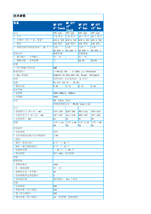
0 ℃~+ 40 ℃
-运输和存储
- 20 ℃~+ 60 ℃
·相对湿度
最大 90%; 没有浓缩
功能
报警系统
·报警的数目
4000
·位 /模拟报警
有/有
·报警的长度(字符数)
80
·每条报警的过程值数目
8
·消息缓冲器
循环缓冲, 512 个消息
对象
·过程画面
500
·变量对象(每个画面)
200
·域(每个画面)
200
·图形对象(每个画面)
10 (柱型图,趋势曲线)
·配方 - 数据纪录 - 条目 可组态的系统键 图形 /图形列表 变量 用户管理 在线连接(同时) 在线语言(同时) 屏幕上的键盘 清空屏幕 字体
安全系统(密码 保护) 帮助系统 VBScript 脚本 趋势 图形对象 文本对象 任务计划(计时 功能) 可选件
227×167 311×249 339×207 434×291
·安装深度( mm)
61
61
61
55
重量 环境条件
大约 1.61 大约 2.65 大约 2.25 大约 4.95
kg
kg
kg
kg
·安装角度
垂直
- 无外部通风的最大允许倾斜角
±35°
·温度
-操作(垂直安装)
0 ℃~+ 50 ℃
-操作(最大倾斜角度)
附加功能 订货号
300
500
1000
有
有
有
2048
有
6
5
有
有
无
WinCC flexible 标准字体 , Tahoma 字体 , 符 号语言 … 有
GD选型表——精选推荐

GD选型表Flash SRAM GPTM (16bit)Advanced TM (16bit)Basic TM(16bit)SysTick (24bit)WDG RTC USART (UART)I 2CSPI CAN 2.0B USB 2.0 FS I 2S SDIOEther-net 12bit ADCUnits (CHs)12bit DACUnitsGD32F103T4U610816K 6K up to 2621121211112(10)QFN36GD32F103T6U610832K 10K up to2621121211112(10)QFN36GD32F103T8U610864K 20K up to 2631121211112(10)QFN36GD32F103TBU6108128K 20K up to 2631121211112(10)QFN36GD32F103C4T610816K 6K up to 3721121211112(10)LQFP48GD32F103C6T610832K 10K up to 3721121211112(10)LQFP48GD32F103C8T610864K 20K up to3731121322112(10)LQFP48GD32F103CBT6108128K 20K up to 3731121322112(10)LQFP48GD32F103R4T610816K 6K up to 5121121211112(16)LQFP64GD32F103R6T610832K 10K up to 5121121211112(16)LQFP64GD32F103R8T610864K 20K up to 5131121322112(16)LQFP64GD32F103RBT6108128K 20K up to5131121322112(16)LQFP64GD32F103RCT6108256K 48K up to5142212152311213(16)2LQFP64GD32F103RDT6108384K 64K up to5142212152311213(16)2LQFP64GD32F103RET6108512K 64K up to5142212152311213(16)2LQFP64GD32F103RFT6108768K 96K up to51102212152311213(16)2LQFP64GD32F103RGT61081024K 96K up to51102212152311213(16)2LQFP64GD32F103RIT61082048K 96K up to51102212152311213(16)2LQFP64GD32F103RKT61083072K 96K up to 51102212152311213(16)2LQFP64GD32F103V8T610864K 20K up to 803112132211●2(16)LQFP100GD32F103VBT6108128K 20K up to 803112132211●2(16)LQFP100GD32F103VCT6108256K 48K up to804221215231121●3(16)2LQFP100GD32F103VDT6108384K 64K up to804221215231121●3(16)2LQFP100GD32F103VET6108512K 64K up to804221215231121●3(16)2LQFP100GD32F103VFT6108768K 96K up to8010221215231121●3(16)2LQFP100GD32F103VGT61081024K 96K up to8010221215231121●3(16)2LQFP100GD32F103VIT61082048K 96K up to8010221215231121●3(16)2LQFP100GD32F103VKT61083072K 96K up to8010221215231121●3(16)2LQFP100GD32F103ZCT6108256K48Kup to 1124221215231121●3(21)2LQFP144G D 32F 10332-bit ARM ? Cortex ?-M3 MCUs Selection Guide (Jul/2015)S e r i e sPart No.MaxSpeed(MHz)Memory(Bytes)I/O TimerEXMCAnalog Interface Package ConnectivityFlash SRAM GPTM (16bit)Advanced TM (16bit)Basic TM (16bit)SysTick (24bit)WDG RTC USART (UART)I 2 CSPI CAN 2.0B USB 2.0 FS I 2S SDIOEther-net 12bit ADC Units (CHs)12bit DACUnits32-bit ARM ? Cortex ?-M3 MCUs Selection Guide (Jul/2015)S e r i e sPart No.MaxSpeed(MHz)Memory(Bytes)I/O TimerEXMC Analog Interface Package ConnectivityGD32F103ZDT6108384K 64K up to 1124221215231121●3(21)2LQFP144GD32F103ZET6108512K 64K up to 1124221215231121●3(21)2LQFP144GD32F103ZFT6108768K 96K up to11210221215231121●3(21)2LQFP144GD32F103ZGT61081024K 96K up to11210221215231121●3(21)2LQFP144GD32F103ZIT61082048K 96K up to11210221215231121●3(21)2LQFP144GD32F103ZKT61083072K 96K up to 11210221215231121●3(21)2LQFP144GD32F105R8T610864K 64K up to 514121215232OTG 22(16)2LQFP64GD32F105RBT6108128K 64K up to 514121215232OTG 22(16)2LQFP64GD32F105RCT6108256K 96K up to 514121215232OTG22(16)2LQFP64GD32F105RDT6108384K 96K up to 514221215232OTG 22(16)2LQFP64GD32F105RET6108512K 96K up to 514221215232OTG 22(16)2LQFP64GD32F105RFT6108768K 96K up to 5110221215232OTG22(16)2LQFP64GD32F105RGT61081024K 96K up to 5110221215232OTG 22(16)2LQFP64GD32F105V8T610864K 64K up to 804121215232OTG2●2(16)2LQFP100GD32F105VBT6108128K 64K up to 804121215232OTG 2●2(16)2LQFP100GD32F105VCT6108256K 96K up to 804121215232OTG 2●2(16)2LQFP100GD32F105VDT6108384K 96K up to 804221215232OTG2●2(16)2LQFP100GD32F105VET6108512K 96K up to 804221215232OTG 2●2(16)2LQFP100GD32F105VFT6108768K 96K up to 8010221215232OTG 2●2(16)2LQFP100GD32F105VGT61081024K 96K up to 8010221215232OTG2●2(16)2LQFP100GD32F105ZCT6108256K 96K up to 1124221215232OTG 2●2(21)2LQFP144GD32F105ZDT6108384K 96K up to 1124221215232OTG 2●2(21)2LQFP144GD32F105ZET6108512K 96K up to 1124221215232OTG2●2(21)2LQFP144GD32F105ZFT6108768K 96K up to 11210221215232OTG2●2(21)2LQFP144GD32F105ZGT61081024K 96K up to 11210221215232OTG 2●2(21)2LQFP144GD32F107RBT6108128K 96K up to 514121215132OTG 2●2(16)2LQFP64GD32F107RCT6108256K 96K up to 514121215132OTG 2●2(16)2LQFP64GD32F107RDT6108384K 96K up to 514221215232OTG2●2(16)2LQFP64GD32F107RET6108512K96Kup to 514221215232OTG2●2(16)2LQFP64G D 32F 107G D 32F 105G D 32F 103Flash SRAM GPTM (16bit)Advanced TM (16bit)Basic TM (16bit)SysTick (24bit)WDG RTC USART (UART)I 2CSPI CAN 2.0B USB 2.0 FS I 2S SDIOEther-net 12bit ADC Units (CHs)12bit DACUnits32-bit ARM ? Cortex ?-M3 MCUs Selection Guide (Jul/2015)S e r i e sPart No.MaxSpeed(MHz)Memory(Bytes)I/O TimerEXMCAnalog Interface Package ConnectivityGD32F107RFT6108768K 96K up to 5110221215232OTG 2●2(16)2LQFP64GD32F107RGT61081024K 96K up to 5110221215232OTG 2●2(16)2LQFP64GD32F107VBT6108128K 96K up to 804121215132OTG2●●2(16)2LQFP100GD32F107VCT6108256K 96K up to 804121215132OTG2●●2(16)2LQFP100GD32F107VDT6108384K 96K up to 804221215232OTG2●●2(16)2LQFP100GD32F107VET6108512K 96K up to 804221215232OTG2●●2(16)2LQFP100GD32F107VFT6108768K 96K up to 8010221215232OTG2●●2(16)2LQFP100GD32F107VGT61081024K 96K up to 8010221215232OTG2●●2(16)2LQFP100GD32F107ZCT6108256K 96K up to 1124221215232OTG2●●2(21)2LQFP144GD32F107ZDT6108384K 96K up to 1124221215232OTG2●●2(21)2LQFP144GD32F107ZET6108512K 96K up to 1124221215232OTG2●●2(21)2LQFP144GD32F107ZFT6108768K 96K up to 11210221215232OTG2●●2(21)2LQFP144GD32F107ZGT61081024K 96K up to 11210221215232OTG2●●2(21)2LQFP144GD32F101T4U65616K 4K up to 2621212111(10)QFN36GD32F101T6U65632K 6K up to2621212111(10)QFN36GD32F101T8U65664K 10K up to 2631212111(10)QFN36GD32F101TBU656128K 16K up to 2631212111(10)QFN36GD32F101C4T65616K 4K up to 3721212111(10)LQFP48GD32F101C6T65632K 6K up to 3721212111(10)LQFP48GD32F101C8T65664K 10K up to 3731213221(10)LQFP48GD32F101CBT656128K 16K up to3731213221(10)LQFP48GD32F101R4T65616K 4K up to 5121212111(16)LQFP64GD32F101R6T65632K 6K up to 5121212111(16)LQFP64GD32F101R8T65664K 10K up to 5131213221(16)LQFP64GD32F101RBT656128K 16K up to 5131213221(16)LQFP64GD32F101RCT656256K 32K up to 51421215231(16)LQFP64GD32F101RDT656384K 48K up to 51421215231(16)LQFP64GD32F101RET656512K 48K up to 51421215231(16)LQFP64GD32F101RFT656768K 80K up to 511021215232(16)LQFP64GD32F101RGT6561024K80Kup to 511021215232(16)LQFP64G D 32F 107G D 32F 101Flash SRAM GPTM (16bit)Advanced TM (16bit)Basic TM (16bit)SysTick (24bit)WDG RTC USART (UART)CSPI CAN 2.0B USB 2.0 FS I 2S SDIOEther-net 12bit ADC Units (CHs)12bit DAC Units32-bit ARM ? Cortex ?-M3 MCUs Selection Guide (Jul/2015)S e r i e sPart No.MaxSpeed(MHz)Memory(Bytes)I/OTimerEXMCAnalog Interface Package ConnectivityGD32F101RIT6562048K 80K up to 511021215232(16)LQFP64GD32F101RKT6563072K 80K up to 511021215232(16)LQFP64GD32F101V8T65664K 10K up to 803121322●1(16)LQFP100GD32F101VBT656128K 16K up to 803121322●1(16)LQFP100GD32F101VCT656256K 32K up to 8042121523●1(16)LQFP100GD32F101VDT656384K 48K up to 8042121523●1(16)LQFP100GD32F101VET656512K 48K up to 8042121523●1(16)LQFP100GD32F101VFT656768K 80K up to80102121523●2(16)LQFP100GD32F101VGT6561024K 80K up to 80102121523●2(16)LQFP100GD32F101VIT6562048K 80K up to 80102121523●2(16)LQFP100GD32F101VKT6563072K 80K up to80102121523●2(16)LQFP100GD32F101ZCT656256K 32K up to 11242121523●1(16)LQFP144GD32F101ZDT656384K 48K up to 11242121523●1(16)LQFP144GD32F101ZET656512K 48K up to11242121523●1(16)LQFP144GD32F101ZFT656768K 80K up to112102121523●2(16)LQFP144GD32F101ZGT6561024K 80K up to112102121523●2(16)LQFP144GD32F101ZIT6562048K 80K up to 112102121523●2(16)LQFP144GD32F101ZKT6563072K80Kup to 11210212152●2(16)LQFP144G D 32F 101Flash SRAM GPTM (32bit)GPTM (16bit)Advanced TM (16bit)Basic TM (16bit)SysTick(24bit)WDGRTC USART I 2C SPIUSB2.0 FS I 2SCEC12bit ADC Units (CHs)12bit DACUnitsGD32F130F4P64816K 4K up to 151411211111(9)TSSOP20GD32F130G4U64816K 4K up to231411211111(10)QFN28GD32F130G6U64832K 4K up to 231411212111(10)QFN28GD32F130G8U64864K 8K up to 231511212221(10)QFN28GD32F130K4U64816K 4K up to 271411211111(10)QFN32GD32F130K6U64832K 4K up to 271411212111(10)QFN32GD32F130K8U64864K 8K up to 271511212221(10)QFN32GD32F130C4T64816K 4K up to 391411211111(10)LQFP48GD32F130C6T64832K 4K up to 391411212111(10)LQFP48GD32F130C8T64864K 8K up to 391511212221(10)LQFP48GD32F130R8T64864K 8K up to 551511212221(16)LQFP64GD32F150G4U67216K 4K up to 2415111211111111(10)1QFN28GD32F150G6U67232K 6K up to 2415111212111111(10)1QFN28GD32F150G8U67264K 8K up to 2415111212221111(10)1QFN28GD32F150K4U67216K 4K up to2715111211111111(10)1QFN32GD32F150K6U67232K 6K up to 2715111212111111(10)1QFN32GD32F150K8U67264K 8K up to 2715111212221111(10)1QFN32GD32F150C4T67216K 4K up to3915111211111111(10)1LQFP48GD32F150C6T67232K 6K up to3915111212111111(10)1LQFP48GD32F150C8T67264K 8K up to3915111212221111(10)1LQFP48GD32F150R4T67216K 4K up to5515111211111111(16)1LQFP64GD32F150R6T67232K 6K up to 5515111212111111(16)1LQFP64GD32F150R8T67264K8Kup to 551511212221111(16)1LQFP64G D 32F 130G D 32F 150GD32F1 series of32-bit ARM ? Cortex ?-M3 MCUs Selection Guide (Jul/2015)S e r i e sPart No.Max Speed (MHz)Memory (Bytes)I/OTimerConnectivity Analog InterfacePackageFlash SRAM GPTM (16bit)Adv TM (16bit)Bsc TM(16bit)SysTick (24bit)WDG RTC USART +UART I 2C SPI CAN 2.0B USB 2.0 FS I 2S SDIOLCD -TFT Camera ETH MAC Crypto /Hash 12bit ADC Units (CHs)12bit DACUnits GD32F205RCT6120256K 128K up to 5110221214+2332OTG 213(16)2LQFP64GD32F205RET6120512K 128K up to 5110221214+2332OTG 213(16)2LQFP64GD32F205RGT61201024K 256K up to 5110221214+2332OTG213(16)2LQFP64GD32F205RKT61203072K 256K up to 5110221214+2332OTG213(16)2LQFP64GD32F205VCT6120256K 128K up to 8210221214+4332OTG2111/03(16)2LQFP100GD32F205VET6120512K128K up to 8210221214+4332OTG 2111/03(16)2LQFP100GD32F205VGT61201024K 256K up to 8210221214+4332OTG 2111/03(16)2LQFP100GD32F205VKT61203072K 256K up to 8210221214+4332OTG2111/03(16)2LQFP100GD32F205ZCT6120256K 128K up to 11410221214+4332OTG2111/13(24)2LQFP144GD32F205ZET6120512K128K up to 11410221214+4332OTG 2111/13(24)2LQFP144GD32F205ZGT61201024K 256K up to 11410221214+4332OTG 2111/13(24)2LQFP144GD32F205ZKT61203072K 256K up to 11410221214+4332OTG 2111/13(24)2LQFP144GD32F207RCT6120256K 128K up to 5110221214+2332OTG211113(16)2LQFP64GD32F207RET6120512K128K up to 5110221214+2332OTG 211113(16)2LQFP64GD32F207RGT61201024K 256K up to 5110221214+2332OTG 211113(16)2LQFP64GD32F207RKT61203072K 256K up to 5110221214+2332OTG211113(16)2LQFP64GD32F207VCT6120256K 128K up to 8210221214+4332OTG2111111/03(16)2LQFP100GD32F207VET6120512K128K up to 8210221214+4332OTG 2111111/03(16)2LQFP100GD32F207VGT61201024K 256K up to 8210221214+4332OTG 2111111/03(16)2LQFP100GD32F207VKT61203072K 256K up to 8210221214+4332OTG2111111/03(16)2LQFP100GD32F207ZCT6120256K 128K up to 11410221214+4332OTG2111111/13(24)2LQFP144GD32F207ZET6120512K128K up to 11410221214+4332OTG 2111111/13(24)2LQFP144GD32F207ZGT61201024K 256K up to 11410221214+4332OTG 2111111/13(24)2LQFP144GD32F207ZKT61203072K 256K up to 11410221214+4332OTG2111111/13(24)2LQFP144GD32F207IET6120512K128K up to 14010221214+4332OTG 2111111/13(24)2LQFP176GD32F207IGT61201024K 256K up to 14010221214+4332OTG 2111111/13(24)2LQFP176GD32F207IKT61203072K 256K up to 14010221214+4332OTG2111111/13(24)2LQFP176Package G D 32F 205G D 32F 207GD32F2 series of32-bit ARM ? Cortex ?-M3 MCUs Selection Guide (Jul/2015) S e r i e sPart No.MaxSpeed(MHz)Memory(Bytes)I/OTimerConnectivityEXMC/SDRAM Analog Interface。
Product_Spec_MT4601B02-1_Ver.1.1_20120803_201308232462
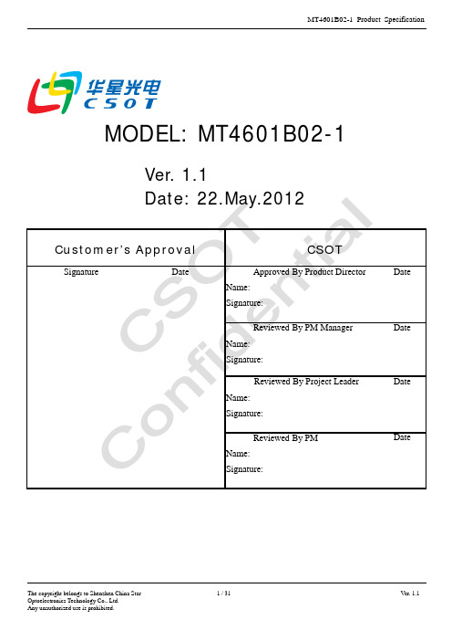
MT4601B02-1 Product SpecificationVer. 1.1ContentsRevision History (4)1. General Description (5)1.1 Product Features (5)1.2 Overview (5)1.3 General Information (5)2. Absolute Maximum Ratings (6)2.1 Absolute Maximum Ratings (Ta = 25 ± 2 °C) (6)2.2 Environment Requirement (6)2.3 Package Storage (7)3. Electrical Specification (8)3.1 Electrical Characteristics (8)3.1.1 Power Consumption (Ta = 25 ± 2 ºC) (8)3.1.2 LVDS Characteristics (9)3.2 Backlight Converter Unit (10)3.2.1 LED Converter Electrical Characteristics (Ta = 25 ± 2 ºC) (10)3.2.2 LED Converter Power Sequence (11)4. Electrical Block Diagram (12)5. Input Terminal Pin Assignment (13)5.1 TFT LCD Module (13)5.2 Converter Unit (15)5.2.1 Converter Input Connector Pin Definition (15)5.3 Block Diagram of Interface (16)5.4 LVDS Interface (16)5.4.1 VESA Format (SELLVDS = H) (16)5.4.2 JEIDA Format (SELLVDS = L or Open) (16)5.5 Color Data Input Assignment (17)6. Interface Timing (18)6.1 Timing Table (DE Only Mode) (18)6.2 Power On/Off Sequence (19)7. Optical Characteristics (20)7.1 Measurement Conditions (20)7.2 Optical Specifications (21)8. Mechanical Characteristics (25)8.1 Mechanical Specification (25)8.2 Packing (27)8.2.1 Packing Specifications (27)8.2.2 Packing Method (27)9. Definition of Labels (29)9.1 Module Label (29)9.2 Carton Label (29)9.3 Pallet Label (30)10. Precautions (31)10.1 Assembly and Handling Precautions (31)10.2 Safety Precautions (31)Revision History1. General Description1.1 Product Features-FHD Resolution (1920 x 1080)-High Brightness: 350 cd/m²-Very High Contrast Ratio: 4000:1-Fast Response Time-High Color Saturation: 72% NTSC-Ultra Wide Viewing Angle: 178° (H)/178° (V) (CR ≥ 10) -Low Power Consumption: Typ. 85 W2. Absolute Maximum Ratings2.1 Absolute Maximum Ratings (Ta = 25 ± 2 °C)The followings are maximum values which, if exceeded, may cause damage to the unit.The maximum operating temperature is based on the test condition that the surface temperature of display area is less than or equal to 65 ºC with LCD module in a temperature controlled chamber alone. Thermal management should be considered in final product design to prevent the surface temperature of display area from being over 65 ºC. The range of operating temperature may degrade in case of improper thermal management in the end product design.(3) The TFT module including glass should be avoided any shock or vibration.While testing shock and vibration, the fixture holding the module should be assured to be hard and rigid enough to prevent the module twisted or bent by the fixture. The test conditions should be less than:Shock (Non-operating): 35 G, 11 ms, half sine wave, 1 time for ± X, ± Y, ± Z.Vibration (Non-operating): Random 1.0 Grms, 10 ~ 200 Hz, 10 min, 1 time for each X, Y, Z.2.3 Package StorageWhen storing modules as spares for a long time, please follow the precaution instructions:(1) Do not store the module in high temperature and high humidity for a long time. It is highly recommended to store themodule with temperature from 0 ºC to 35 ºC in normal humidity.(2) The module shall be stored in a dark area and avoided to be exposed in direct sunlight or fluorescent light.3. Electrical Specification3.1 Electrical CharacteristicsFig. 3.2 Test patterns3.2 Backlight Converter UnitFig. 3.5 The power sequence of V BL and V BLONNOTE:The power sequence :POWER ON : V BL > V P_DIM >V BLON POWER OFF :V BLON >= V P_DIM> V BLV V V4. Electrical Block Diagram5. Input Terminal Pin Assignment5.1 TFT LCD ModuleCN1: 0-511037-5 (Xi Da Yi Tong) or equivalent (see Note (1))CN1(6)Fig. 5.1 LVDS connector direction sketch map(2) For CSOT internal only, please let it open.(3) High: connect to + 3.3 V →VESA format; Low: connect to GND or Open →JEIDA format.5.2 Converter Unit5.2.1 Converter Input Connector Pin DefinitionCN1: CI0114M1HR0-NH (Cvilux) or equivalent (see 5.2 Note (1))Fig. 5.2 Power input connector direction sketch map Attention:If the external PWM function includes 10% dimming ratio, the judge conditions are as below:(1) Backlight module must be lighted on normally.(2) All protection functions must work normally.(3) Uniformity and flicker could not be guaranteed.5.3 Block Diagram of InterfaceFig. 5.5 JEIDA format5.5 Color Data Input AssignmentThe brightness of each primary color is based on the 8-bit gray scale data input for each color. The higher the binary input, the brighter the color. The table below provides the assignment of the color versus.Attention:0: Low level voltage; 1: High level voltage.6. Interface TimingFig. 6.1 Interface signal timing diagram6.2 Power On/Off SequenceTo prevent a latch-up or DC operation of LCD module, the power on/off sequence should be as the diagram below.(2) Apply the lightbar voltage within the LCD operation range. When the backlight turns on before the LCD operation or theLCD turns off before the backlight turns off, the display may momentarily become abnormal screen.(3) In case that V CC is in off level, please keep the level of input signals on the low or high impedance. If T2 < 0, that maycause electrical overstress.(4) T4 should be measured after the module has been fully discharged between power off and on period.(5) Interface signal shall not be kept at high impedance when the power is on.7. Optical Characteristics7.1 Measurement ConditionsThe table below is the test condition of optical measurement.N means the actual number of the pixels in the area S.7.2 Optical SpecificationsThe table below of optical characteristics is measured by MINOLTA CS2000, MINOLTA CA310, ELDIM OPTI Scope-SA and ELDIM EZContrast in dark room.CR-W is the luminance measured by LMD(light-measuring device) at the center point of the LCD module with full-screen displaying white. The standard setup of measurement is illustrated in Fig. 7.3;CR-D is the luminance measured by LMD at the center point of the LCD module with full-screen displaying black.(2) The LMD in the item could be a spectroradiometer such as (KONICA MINOLTA) CS2000, CS1000, (TOPCON) SR-UL2or the same level spectroradiometer. Other display color analyzer (KONICA MINOLTA) CA210, CA310 or (TOPCON) BM-7 could be involved after being calibrated with a spectroradiometer on each stage of a product.Fig. 7.3 The standard setup of CR measurement(3) Response time T L is defined as the average transition time in the response time matrix. The table below is the responseX to YAll the transition time is measured at the center point of the LCD module by ELDIM OPTI Scope-SA.(4) Definition of center luminance (L W):The luminance is measured at the center point of the LCD module with full-screen displaying white. Fig. 7.5 shows the standard setup of luminance measurement.and themin Uniformity=L(6)color R,G,B and white.G,Bcoordinates and the area is defined by NTSC1953color standard in the CIE color space.Chromaticity coordinates are measured by CS2000 and the standard setup of measurement is shown in Fig. 7.7.Fig. 7.7 The standard setup of color chromaticity measurement (7) Definition of viewing angle coordinate system (θH, θV):angles: upθV+8. Mechanical Characteristics 8.1 Mechanical Specification8.2 PackingFig. 8.1 Packing method (protector film stick on the front of the LCD module)Protector Film LCD Module PE BagCorrugated BoardPP BeltCarton LabelTop CushionMasking TapePalletBottom CushionAround BoardLCD ModuleEarth CoverPallet Label PalletPE FilmPE SheetPP BeltFig. 8.2 Shipping method9. Definition of Labels 9.1 Module LabelManufactured Date:Year: 2010 = 10, 2011 = 11…2020 = 20, 2021 = 21…9.3 Pallet LabelSerial Number: XXX XX XXX XXXXXCSOT Internal UseYear, MonthMT4601B02-1 Product Specification 10. Precautions10.1 Assembly and Handling Precautions(1) Do not apply rough force such as bending or twisting to the LCD module during assembly.(2) It is recommended to assemble or install a LCD module into the user’s system in clean working areas. The dustand oil may cause electrical short or damage the polarizer.(3) Do not apply pressure or impulse to the LCD module to prevent the damage to LCD panel and backlight.(4) Always follow the correct power-on sequence. This can prevent the damage and latch-up to the LSI chips.(5) Do not plug in or pull out the interface connector while the module is in operation.(6) Do not disassemble the LCD module.(7) Use soft dry cloth without chemicals for cleaning because the surface of polarizer is very soft and easily bescratched.(8) Moisture can easily penetrate into the LCD module and may cause the damage during operation.(9) High temperature or humidity may deteriorate the performance of the LCD module. Please store LCD modules inthe specified storage conditions.(10) When ambient temperature is lower than 10ºC, the display quality might be deteriorated. For example, theresponse time will become slow, and the starting voltage of LED light bar will be higher than that in roomtemperature.10.2 Safety Precautions(1) If the liquid crystal material leaks from the panel, it should be kept away from the eyes or mouth. In case ofcontact with hands, skin or clothes, it has to be washed away thoroughly with soap.(2) After the LCD module’s end of life, it is not harmful in case of normal operation and storage.The copyright belongs to Shenzhen China Star 31 / 31 Ver. 1.1 Optoelectronics Technology Co., Ltd.Any unauthorized use is prohibited.。
OTHER(其它)液晶面板连接器型号清单--精电连接
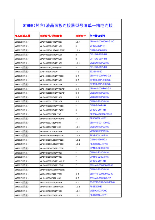
MSB240420HE DF9C-31P-1V MSB24013P20HA MSB24013P20HA DF19G-20P-1H DF19G-20P-1H 08-6210-033-340-800A+ 076B20-0048RA-G4 076B20-0048RA-G4 DF19L-20P-1H DF19K-20P-1H DF19K-20P-1H DF19K-20P-1H 089N40-000R00-G2 FI-XB30SSL-HF15 FI-SEB20P-HFE FI-SEB20P-HFE FI-RE51S-HF FI-RE51S-HF FI-E30S FI-E30S FI-X30SSL-HF FI-X30SSL-HF FI-X30SSL-HF FI-X30SSL-HF FI-RE51S-HF FI-RE51S-HF FI-RE51S-HF FI-RE51S-HF FI-RE51S-HF FI-RE51S-HF FI-RE51S-HF FI-RE51S-HF IS100-L30O-C23 DF14H-20P-1.25H DF9B-31P-1V FH12-20S-0.5SH FH12-20S-0.5SH FH12-20S-0.5SH FH12-20S-0.5SH FH12-20S-0.5SH FH12-20S-0.5SH
OTHER(其它)液晶面板连接器型号清单--精电连接
液晶面板品牌
AMPIRE(晶采) AMPIRE(晶采) AMPIRE(晶采) AMPIRE(晶采) AMPIRE(晶采) AMPIRE(晶采) AMPIRE(晶采) AMPIRE(晶采) AMPIRE(晶采) AMPIRE(晶采) AMPIRE(晶采) AMPIRE(晶采) AMPIRE(晶采) AMPIRE(晶采) AMPIRE(晶采) AMPIRE(晶采) AMPIRE(晶采) AMPIRE(晶采) AMPIRE(晶采) AMPIRE(晶采) AMPIRE(晶采) AMPIRE(晶采) AMPIRE(晶采) AMPIRE(晶采) AMPIRE(晶采) AMPIRE(晶采) AMPIRE(晶采) AMPIRE(晶采) AMPIRE(晶采) AMPIRE(晶采) AMPIRE(晶采) AMPIRE(晶采) AMPIRE(晶采) AMPIRE(晶采) AMPIRE(晶采) AMPIRE(晶采) AMPIRE(晶采)