OB3330X 中文
SPD3303X_QuickStart_QS0503X-C01A

本产品上使用的标记 本产品上可能出现如下标记:
警告高压
保护性终端
小心
测量接地端
电源开关
IV SPD3303X 面板功能介绍
SIGLENT
SPD3303X 简介
SPD3303X 直流电源,轻便,可调,多功能工作配置。它具有三组独立输出:两 组可调电压值和一组固定可选择电压值 2.5V、3.3V、和 5V,同时具有输出短路和过 载保护。
SPD3303X 可编程线性直流电源
面板功能介绍
2016 深圳市鼎阳科技有限公司
版权和声明
SIGLENT
版权
深圳市鼎阳科技有限公司版权所有
商标信息
SIGLENT 是深圳市鼎阳科技有限公司的注册商标
声明
本公司产品受已获准及尚在审批的中华人民共和国专利的保护。 本公司保留改变规格及价格的权利。 本手册提供的信息取代以往出版的所有资料。 未经本公司许可,不得以任何形式或手段复制、摘抄、翻译本手册的内容。
VI SPD3303X 面板功能介绍
SIGLENT
3.3 命令说明................................................................................................................... 29 第四章 常见故障处理...........................................................................................................36 第五章 服务和支持...............................................................................................................37
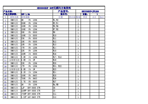
OB3330XCP 50W+JW1221 驱动BOM
1206 1206 1206 1206 0805 0805 0805 0805 1206 1206 1206 0805 1206 1W 1206 1206 1W 1206 0603 0603 0805 1206 0805 X7R 0805 X7R 0805 X7R 0603 X7R
OB3330XCP+JW1220 版本号: 页数: 1 位置 供应商 数量 单价 合计 备注 R1,R2 2 R3,R4 2 R5,R6 2 R7,R8 2 R9 1 R10 1 R11 1 R12 1 R13 1 R14 1 R15 1 R16 1 R17,R18 2 R19 1 R20 1 R21,R22 2 R23 1 R24 1 R25 1 R26 1 R27 1 RA,RB 2 C6 1 C5 1 C11 1 C12 1
产品名称: 产品主要参数: SMD电容 27 SMD电容 28 29 SMD二极体 30 SMD二极体 Y电容 31 涤纶电容 32 保险管 33 热敏电阻 34 压敏电阻 35 环形电感 36 37 38 39 40 41 42 43 44 45 46 47 48 49 50 工字电感 环形电感 环形电感 X2电容 X2电容 整流桥 CBB电容 MOS管 MOS管 散热器 变压器 电解电容 电解电容 电解电容
OB3330XCP 50W无频闪方案资料 产品型号:
35V 1.5A 材料规格 2M 5% 200K 5% 100K 5% 100K 5% 20K 5% 100K 1% 33K 5% 10K 5% 10R 5% 47R 5% 22K 5% 150R 1% 3.0R 1% 0.5R 1% 22K 5% 47R 5% 0.5R 1% 0.1R 1% 100K 5% 750K 5% 4.7K 5% 1M 5% 1uF 50V 220PF 50V 470NF 50V 2.2UF 16V
3300系列耐用封闭型磁电流表关闭阀门闸控制、警报和限位用途说明书

3300 Series RuggedSeal Meter Relay• Wide Variety of Control, Alarm, and Limit Use• Calibration Not Affected by Steel Panel Mounting• Rugged Metal Case for Rigorous EnvironmentsOrdering Information-DC Microammeters, Self-Shielding MovementRangeApprox.Resistance(ohms)Model/Size and Catalog Number3-1/2” Model3323AIXA4-1/2” Model3324AIXASingle Set point(High Limit)DualSet pointSingle Set point(High Limit)DualSet point0 - 252k2165821618<><> 0 - 501k21659216192166621626 0 - 10050021660216202166721627<> Available on special orderDC Milliammeters, Self-Shielding MovementRangeApprox.Resistance(ohms)Model/Size and Catalog Number3-1/2” Model3323AIXA4-1/2” Model3324AIXASingle Set point(High Limit)DualSet pointSingle Set point(High Limit)DualSet point0 - 150216612162121668216283300 Series RuggedSeal Meter Relay Ordering Information -DC Millivoltmeters, Self-Shielding MovementRangeApprox.Resistance(ohms)Model/Size and Catalog Number3-1/2” Model3323AIXA4-1/2” Model3324AIXASingle Set point(High Limit)DualSet pointSingle Set point(High Limit)DualSet point0 - 501k21663216232167021630 DC Voltmeters, Self-Shielding MovementRangeApprox.Resistance(ohms)Model/Size and Catalog Number3-1/2” Model3323AIXA4-1/2” Model3324AIXASingle Set point(High Limit)DualSet pointSingle Set point(High Limit)DualSet point0 - 120k21664216242167121631 0 - 501M21665216252167221632DC Ammeters, Self-Shielding MovementRangeApprox.Impedance(ohms)Model/Size and Catalog Number3-1/2” Model3323AIXA4-1/2” Model3324AIXASingle Set point(High Limit)DualSet pointSingle Set point(High Limit)DualSet point0 - 5.0121662216222166921629 Percent Motor Load, Self-Shielding MovementScale Range F.S.Catalog NumberSingle Set point(High Limit)Catalog NumberDouble Set point Model0-150 *10 VAC21684 * 21644 *3344 AIXA 4-1/2”0-150 ** 5 amp AC21683 **21643 **3344 AIXA 4-1/2”0-150 ** 5 amp AC35096 **35097 **3343 AIXA 3-1/2”* Use with Model 186 current transformers** Use with current transformers3300 Series Rugged Seal Meter Relay3300 Series RuggedSeal Meter RelayTemperature MetersOrdering Information -Temperature Range ThermocoupleTypeCatalog NumberModel# 3324 AIXA 4-1/2”SSP DSP0 to 300°F (0°C to +149°C)Type J 21651216110 to 500°F (0°C to +260°C)2165221612 0 to 750°F (0°C to +399°C)2165321613 0 to 1000°F (0°C to +538°C2165421614 0 to 1500°F (0°C to +815°C)Type K2165521615 0 to 2500°F (0°C to +1371°C)2165721617 Thermocouples are not supplied. Available separately from Accessory Section3300 Series RuggedSeal Meter Relay Dimensions4 - 1/2” - Model 3344AIXA & 3324AIXA3 - 1/2”- Model 3343AIXA & 3323AIXASimpson Electric Co.520 Simpson Ave.Lac du Flambeau, Wi 54538Ph: (715) 588-3311。
XX1000-QT-0G00中文资料
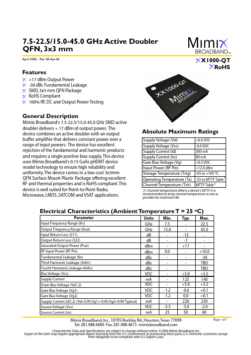
7.5-22.5/15.0-45.0 GHz Active Doubler +17 dBm Output Power-30 dBc Fundamental Leakage SMD, 3x3 mm QFN Package RoHS Compliant100% RF, DC and Output Power TestingFeaturesElectrical Characteristics (Ambient T emperature T = 25 o C)ParameterInput Frequency Range (fin)Output Frequency Range (fout)Input Return Loss (S11)Output Return Loss (S22)Saturated Output Power (Psat)RF Input Power (RF Pin)Fundamental Leakage (fin)Third Harmonic Leakage (3xfin)Fourth Harmonic Leakage (4xfin)Bias Voltage (Vcc)Supply CurrentUnits GHz GHz dB dB dBm dBm dBc dBc dBc VDC mA Min.7.515.0---0.0-----Typ.---15-7+17----+5.0125Max.22.545.0---+10.0-30TBD TBD +5.5140April 2006 - Rev 28-Apr-06Drain Bias Voltage (Vd1,2)Gate Bias Voltage (Vg1)Gate Bias Voltage (Vg2)Supply Current (Id1,2) (Vd=5.0V, Vg1=-0.6V, Vg2=0.0V Typical)Source Voltage (Vss)Source Current (Iss)VDC VDC VDC mA VDC mA --1.2-1.2--5.525+5.0-0.60.0220-5.050+5.5+0.1+0.1250-2.060Absolute Maximum RatingsSupply Voltage (Vd)Supply Voltage (Vss)Supply Current (Id)Supply Current (Iss)Gate Bias Voltage (Vg)Input Power (RF Pin)Storage Temperature (Tstg)Operating Temperature (Ta)Channel Temperature (Tch)+6.0 VDC -6.0 VDC 300 mA 60 mA +0.3 VDC +12.0 dBm -65 to +165 O C -55 to MTTF Table MTTF Table 1(1) Channel temperature affects a device's MTTF. It is recommended to keep channel temperature as low as possible for maximum life.1Mimix Broadband's 7.5-22.5/15.0-45.0 GHz SMD active doubler delivers + 17 dBm of output power. The device combines an active doubler with an output buffer amplifier that delivers constant power over a range of input powers. The device has excellent rejection of the fundamental and harmonic products and requires a single positive bias supply. This device uses Mimix Broadband's 0.15 GaAs pHEMT device model technology to ensure high reliability and uniformity. The device comes in a low-cost 3x3mm QFN Surface Mount Plastic Package offering excellent RF and thermal properties and is RoHS compliant. This device is well suited for Point-to-Point Radio,Microwave, LMDS, SATCOM and VSAT applications.General DescriptionDoubler Measurements7.5-22.5/15.0-45.0 GHz Active DoublerPout for P in = 0 to 10dBm -30-20-10102030791113151719212325Fin (GH z)P o u t (d B m )1Power Sweep for Fin = 10GHz -30-25-20-15-10-50510152025-15-10-5051015Pin (dB m)P o u t (d B m )11. Measured results taken at room temperature in 40 GHz connectorized test fixture with no de-embedding.April 2006 - Rev 28-Apr-06Doubler Measurements (cont.)7.5-22.5/15.0-45.0 GHz Active DoublerApril 2006 - Rev 28-Apr-06* Measured on-wafer with die version of doubler.* Measured on-wafer with die version of doubler.7.5-22.5/15.0-45.0 GHz Active Doubler (Note: Engineering designator is 40DBL0458QT)Package DimensionsApril 2006 - Rev 28-Apr-06XX1000-QT wwwwwww P xxxx GTop ViewBottom ViewPin 3 5 6 7 10 13 15DescriptionRF InVg1VssVg2RF OutVd2Vd17.5-22.5/15.0-45.0 GHz Active DoublerApp Note [1] Biasing - It is recommended to separately bias each doubler stage with Vd(1,2)=5.0V with Id1=80mA and Id2=140mA and Vss=-5.0V with Iss=50mA. XX1000-QT provides good performance at reduced bias with Vss=-2.0V and Iss=25mA. Maximum output power is achieved with Vss=-5.0V and Iss=50mA. Separate biasing is recommended if the doubler is to be used at high levels of saturation, where gate rectification will alter the effective gate control voltage. It is also recommended to use active biasing to keep the currents constant as the RF power and temperature vary; this gives the most reproducible results. Depending on the supply voltage available and the power dissipation constraints, the bias circuit may be a single transistor or a low power operational amplifier, with a low value resistor in series with the drain supply used to sense the current. The gate of the pHEMT is controlled to maintain correct drain current and thus drain voltage. The typical gate voltages needed to do this are Vg1=-0.6V and Vg2=0.0V. Typically the gate is protected with Silicon diodes to limit the applied voltage. Also, make sure to sequence the applied voltage to ensure negative gate bias is available before applying the positive drain supply.MTTF T ables (TBD)These numbers were calculated based on accelerated life test information and thermal model analysis received from the fabricating foundry.Backplate Temperature 55 deg Celsius 75 deg Celsius 95 deg CelsiusChannelTemperaturedeg Celsiusdeg Celsiusdeg CelsiusFITsE+E+E+MTTF HoursE+E+E+RthC/WC/WC/WBias Conditions: Vd1=Vd2=4.0V, Id1=40 mA, Id2=140 mA, Vss=-5.0V, Iss=50mAApril 2006 - Rev 28-Apr-06 Functional SchematicTop ViewPCB Layout7.5-22.5/15.0-45.0 GHz Active DoublerApril 2006 - Rev 28-Apr-06Application CircuitRF In RF OutVd1Vd2Vg1VssVg2Handling and Assembly InformationCAUTION! - Mimix Broadband MMIC Products contain gallium arsenide (GaAs) which can be hazardous to the human body and the environment. For safety, observe the following procedures:Do not ingest.Do not alter the form of this product into a gas, powder, or liquid through burning, crushing, or chemical processing as these by-products are dangerous to the human body if inhaled, ingested, or swallowed.Observe government laws and company regulations when discarding this product. This product must be discarded in accordance with methods specified by applicable hazardous waste procedures.Life Support Policy - Mimix Broadband's products are not authorized for use as critical components in life support devices or systems without the express written approval of the President and General Counsel of Mimix Broadband. As used herein: (1) Lifesupport devices or systems are devices or systems which, (a) are intended for surgical implant into the body, or (b) support or sustain life, and whose failure to perform when properly used in accordance with instructions for use provided in the labeling, can bereasonably expected to result in a significant injury to the user. (2) A critical component is any component of a life support device or system whose failure to perform can be reasonably expected to cause the failure of the life support device or system, or to affect its safety or effectiveness.Package Attachment - This packaged product from Mimix Broadband is provided as a rugged surface mount package compatible with high volume solder installation. The package is a low-cost plastic package. Vacuum tools or other suitable pick and place equipment may be used to pick and place this part. Care should be taken to ensure that there are no voids or gaps in the solder connection so that good RF, DC and ground connections are maintained. Voids or gaps can eventually lead not only to RF performance degradation, but reduced reliability and life of the product due to thermal stress.Mimix Lead-Free RoHS Compliant Program - Mimix has an active program in place to meet customer and governmentalrequirements for eliminating lead (Pb) and other environmentally hazardous materials from our products. All Mimix RoHS compliant components are form, fit and functional replacements for their non-RoHS equivalents. Lead plating of our RoHS compliant parts is 100% matt tin (Sn) over copper alloy and is backwards compatible with current standard SnPb low-temperature reflow processes as well as higher temperature (260°C reflow) “Pb Free” processes.Part Number for Ordering Description XX1000-QT-0G00 Matte Tin plated RoHS compliant QFN 3x3 16L surface mount package in bulk quantity XX1000-QT-0G0T Matte Tin plated RoHS compliant QFN 3x3 16L surface mount package in tape and reel XX1000-QT-EV1 XX1000-QT Evaluation Board We also offer this part with SnPb (Tin-Lead) or NiPdAu plating. Please contact your regional sales manager for more informationregarding different plating types.Typical Reflow Profiles Reflow Profile Ramp Up RateActivation Time and Temperature Time Above Melting Point Max Peak Temperature Time Within 5 ºC of Peak Ramp Down RateSnPb3-4 ºC/sec60-120 sec @ 140-160 ºC 60-150 sec 240 ºC 10-20 sec 4-6 ºC/secPb Free 3-4 ºC/sec60-180 sec @ 170-200 ºC 60-150 sec 265 ºC 10-20 sec 4-6 ºC/sec7.5-22.5/15.0-45.0 GHz Active DoublerApril 2006 - Rev 28-Apr-06。
Sophos XGS 2100 2300 3100 3300 硬件设备操作说明书

Operating Instructions XGS 2100/2300/3100/3300ForewordWe are pleased to welcome you as a new customer of our Sophos XGS appliances.To install and configure the hardware appliance you can use the following documents:ÌHardware Quick Start Guide: Connection to the system peripherals in a few stepsÌOperating Instructions: Notes on the security andcommissioning of the hardware applianceÌSophos Firewall How-To Library: Installing and configuring the software applianceThe Hardware Quick Start Guide and the Safety Instructions are also delivered in printed form together with the hardware appliance. The instructions must be read carefully prior to using the hardware and should be kept in a safe place.You may download all user manuals and additional documentation from the support webpage at: /supportSecurity SymbolsThe following symbol and its meaning appears in the Hardware Quick Start Guide, Safety Instructions and in these Operating Instructions.Caution and Important note. If these notes are not correctly observed:ÌThis is dangerous to life and the environmentÌThe appliance may be damagedÌThe functions of the appliance will be no longer guaranteedÌSophos shall not be liable for damages arising from afailure to comply with the Safety InstructionsDesigned UseThe hardware appliances are developed for use in networks. XGS 2100/2300/3100/3300 models may be operated as a standalone appliance. The hardware appliance can be used in commercial, industrial and residential environments.The XGS 2100/2300/3100/3300 models belong to the appliance group A.The hardware appliance must be installed pursuant to the current installation notes. Otherwise failure-free and safe operation cannot be guaranteed. The EU declaration of conformity is available at the following address:Sophos Technology GmbHGustav-Stresemann-Ring 165189 WiesbadenGermanyCE Labeling, FCC and Approvals The XGS 2100/2300/3100/3300 appliances comply with CB, CE, UL, FCC, ISED, VCCI, CCC, KC, BSMI, RCM, NOM, Anatel.Important note: For computer systems to remain CE and FCC compliant, only CE and FCC compliant parts may be used. Maintaining CE and FCC compliance also requires proper cable and cabling techniques.Operating Elements and Connections XGS 2100/2300*COM: Micro USB, RJ45, 2 x USB 3.0, MGMT port 1 x expansion bay (shown with optional module)LAN 1–8: 8 x GbE copper – 1 bypass pair (ports 1/2)Multi-function LCD display andnavigation F1–F2 2 x SFP fiber ports XGS 3100/3300*Multi-function LCD display and Navigation 1 x expansion bay (shown with optional module)F3–F4: 2 x SFP fiber ports LAN 1–8: 8 x GbE copper – 1 bypass pair (ports 1/2)F1–F2 2 x SFP+ fiber portsCOM: Micro USB, RJ45, 2 x USB 3.0, MGMT port XGS 2100/2300/3100/3300Power switch Power supply Mounting pins for external power supply Connector for external redundant power supply (available as an option)USB * The displayed front image is of XGS 2300 and XGS 3300 device. The XG 2100 and 3300 device may vary slightly.Interfaces (front)* SFP/SFP+/QSFP transceivers are sold separately.Technical SpecificationsLED StatusLCD and Control Keys The XGS 2100/2300/3100/3300 have an LCD and an operating unit with four membrane keys. In the LCD, 16 characters per line can be displayed.While the security appliance is booting this message is displayed Firmware Version SOPHOS ProtectionFirmware VersionSFOS xx.xx.xxLCD Menu DetailsExecutable Actions ÌFactory reset: All settings are reset to the factory settings. The factory reset function sets all of the configuration settings and options to their original state. All data entered after the initial installation will be deleted, including the HTTP proxy cache, the entire email queue, accounting and reporting data, passwords, and uninstalled Up2Date packages. The version of the software will not change. That is, all firmware and pattern updates that have been installed will be retained. ÌShut down: The security appliance is shut down. The shut down action allows you to turn off the system, and allows you to cleanly stop all running services. ÌReboot machine: The security appliance is rebooted. The reboot action will shut down the system completely and reboot.Control Key Functions The current menu is left. When the key is pressed a couple of times, the modifications are discarded and the initial state will be displayed.These keys are used to switch between the different menus and/or characters.Pressing executes the configured action.Factory ResetShut DownReboot MachinePutting into OperationCaution: Risk of explosion if battery is replaced by an incorrect type. Dispose of used batteries according to the instructions.Scope of SupplyThe supplied parts are indicated in the Hardware Quick Start Guide.Mounting InstructionsThe XGS 2100/2300/3100/3300 appliances are designed for use in racks. Please consider the following security tips:Important note: Functional reliability outside of a rack cannot be guaranteed.Warnings and PrecautionsThe appliance can be operated safely if you observe the following notes and the notes on the appliance itself.Rack PrecautionsÌEnsure that the leveling jacks on the bottom of the rack are fully extendedto the floor with the full weight of the rack resting on them.ÌIn single rack installation, stabilizers should be attached to the rack.ÌIn multiple rack installations, the racks should be coupled together.ÌAlways make sure the rack is stable before extending a component from the rack.ÌYou should extend only one component at a time—extending two ormore simultaneously may cause the rack to become unstable.General Server PrecautionsÌInstallation must be performed by qualified personnelÌReview the electrical and general safety precautions that camewith the components you are adding to your appliance.ÌDetermine the placement of each component in the rack before you install the rails.ÌInstall the heaviest server components on the bottom of the rack first, and then work up.ÌAllow the hot plug power supply modules to cool before touching them.ÌAlways keep the rack‘s front door, all panels and server componentsclosed when not servicing to maintain proper cooling.Rack Mounting ConsiderationsÌAmbient operating temperature: If installed in a closed or multi-unit rack assembly,the ambient operating temperature of the rack environment may be greater than the ambient temperature of the room. Therefore, you should install the equipment in an environment compatible with the manufacturer’s maximum rated ambient temperature.ÌReduced airflow: Equipment should be mounted into arack with sufficient airflow to allow cooling.ÌMechanical loading: Equipment should be mounted into a rack so that ahazardous condition does not arise due to uneven mechanical loading.ÌCircuit overloading: Consideration should be given to the connection of the equipment to the power supply circuitry and the effect that any possible overloading of circuits might have on overcurrent protection and power supply wiring. Appropriate consideration of equipment nameplate ratings should be used when addressing this concern.ÌReliable ground: Reliable grounding must be maintained at all times. To ensurethis, the rack itself should be grounded. Grounding screws for the applianceare on the rear of the chassis. Chassis Grounding is required. Particularattention should be given to power supply connections other than the direct connections to the branch circuit (i.e., the use of power strips, etc.).Rack Mounting InstructionsTo mount the appliance to the rack you need the delivered rack-mount kits. There are a variety of rack units on the market, which may mean the assembly procedure will differ slightly. You should also refer to the installation instructions that came with the rack unit you are using. Please observe the mounting instructions for your rack.Important note: Make sure you use the screws supplied with the rack-mount brackets. Using the wrong screws could damage the hardware appliance and would invalidate your warranty.1. Attach the rack-mount ears to the appliance:ÌPlace the appliance on a hard flat surface with the front panel facing you.Please Note: There are two types of mounting brackets supplied with your appliance. Use the short brackets if you intend to also use sliding rails which are available as an optional accessory from your Sophos partner. Use the long mounting brackets if you don’t want to use additional sliding rails or any other fixation for the appliance.ÌAttach the rack–mount brackets to the left and right sideof the appliance with the supplied screws.ÌMake sure the brackets are properly attached to the appliance.Important note: Please check the technical specs above for the min. and max. rack depth.2. Choose the rack location:ÌLeave enough clearance in front of the rack so that you canopen the front door completely (~60 cm/25 inches).ÌLeave approximately 80 cm/30 inches of clearance in the back ofthe rack to allow for sufficient airflow and ease in servicing.ÌThis product is for installation only in a restricted access location(dedicated equipment rooms, service closets and the like).3. Install the sliding rails (optional):ÌPlease refer to the dedicated Sliding Rails MountingInstructions shipped with the appliance.Please note: If you are using the optional external Power Supply which will be mounted to the rear of your appliance, we strongly recommend using the optional sliding rails.4. In order to prevent the unit from unintentionally sliding out of the rack westrongly recommend fixing the rack-mount brackets to the front rack-mount posts by using screws and nuts supplied with your rack.Connection and ConfigurationHow to connect the appliance is described in the Hardware Quick Start Guide. For configuration you can follow the initial setup wizard described in the WebAdmin Quick Start Guide or cancel it and perform a manual setup (see the Sophos Firewall How-To Library).SFP/SFP+ PortsThe XGS 2100/2300/3100/3300 models offer a variety of SFP/SFP+ ports allowing you to plugin various GBICs (transceivers) to connect to fiber or copper networks. The abbreviation SFP GBIC stands for small form-factore plugable GigaBit interface converter, a flexible interface which changes electronic signals into optical signals. The converters used with the appliance are often also called Mini-GBIC or New GBIC.To use SFP/SFP+ ports, you will need the appropriate transceivers or DAC cables (combining transceivers and cables into one). These are not delivered with the appliance but available through your Sophos partner. There are different module types, and the required type is determined by the existing network.Note: The SFP+ ports of the Sophos FleXi Port modules are dual-rate capable supporting both 1GbE and 10GbE speeds when using appropriate GBICs also supporting both rates. Caution: The SFP and SFP+ ports use lasers to transmit signals over fiber optic cable. The lasers are compliant with the requirements of a Class 1 Laser equipment and are inherently eye-safe in normal operation. However, you should never look directly at a transmitport when it is powered on. Always install appropriate and UL approved Laser Class I Transceivers, rated 3.3Vdc, max. 1W, in the fiber ports before using the fiber ports.Serial ConsoleYou can connect a serial console to either the RJ45 or micro USB COM port to access the CLI. Only one port can be used at any time. If both ports are connected then the micro USB port will take precedence. You can use, for instance, the Hyperterminal terminal program which is included with most versions of Microsoft Windows to log on to the appliance console. If you want to connect to the Micro-USB COM port please use the supplied cable. If you want to connect to the RJ45 COM port please use a RJ45 to DB9 Adapter cable (not provided with the unit). The Pin-out for this cable is shown in the table below.Sophos RJ45 PinoutThis pinout is compatible with Cisco Straight (X2) pinout serial cables.The required connection settings are:ÌBits per second: 38,400ÌData bits: 8ÌParity: N (none)ÌStop bits: 1Access via the serial console is activated by default on ttyS0. The connections of the appliances and the respective functionality are listed in chapter ‘Operating Elements and Connections.’Please Note: If you are connecting to the Micro USB port and it doesn’t show up as COM port but as unknown hardware in your system, please download a Micro USB Driver from https:///drivers/d2xx-drivers/.United Kingdom and Worldwide Sales Tel: +44 (0)8447 671131Email:****************North American SalesToll Free: 1-866-866-2802Email:******************Australia and New Zealand SalesTel: +61 2 9409 9100Email:****************.auAsia SalesTel: +65 62244168Email:********************© Copyright 2021. Sophos Ltd. All rights reserved.Registered in England and Wales No. 2096520, The Pentagon, Abingdon Science Park, Abingdon, OX14 3YP, UK Sophos is the registered trademark of Sophos Ltd. All other product and company names mentioned are trademarks or registered trademarks of their respective owners.。
电力大师3330系列产品介绍说明书

ElectroForce® test instruments incorporate proprietary linear motiontechnologies and WinTest® controls to provide a revolutionaryapproach to mechanical fatigue and dynamic characterization. TheElectroForce family of test instruments provides a full range of forceand performance capabilities for a variety of test applications.The 3330 system provides static to 100 Hz performance with aload envelope of ±3000 N, allowing versatile performance for avariety of test applications such as durability testing of orthopaedicimplant devices and dynamic characterization of engineeredmaterials and components.The ElectroForce High Accuracy Displacement Sensor is the first usein the material testing industry of a new technology that providesdisplacement resolution of a nanometer and accuracies in the rangeof microns. This allows for reliable tests of 10x smaller displacementamplitudes over the full range of motion of the system with noadditional sensors required.ElectroForce® 3330 Series II Table Top andFloor Standing ConfigurationsFirst in the Material Testing IndustryThe design of new materials and products requiresa thorough assessment of material properties andcomplete performance evaluation within theintended end-use service environment. A varietyof basic and advanced testing techniques areavailable in the 3200 to meet this need.• Tension/Compression• Bending• Stress Relaxation• Torsion• Creep• Shear• PulsatileTest TypesElectroForce ® test instruments perform a broad range of materials testing tasks.These requirements range from simple static tests used to acquire tensile , compressive or bending data , to more complex fatigue and fracture mechanics testing applications often found in the following industries and application areas:• Electronics and Microelectronics • Smart Materials • Automotive • Aerospace• Universities and National Labs• Polymers, Plastics, and Composites •Tire and RubberElectroForce testing systems provide a multi-purpose, high performance, clean and reliable product platform that’s well-suited for use in research activities that require mechanical testing.Optional ElectroForce DMA software provides the capability for a ElectroForcematerials testing system to do double duty as a DMA/DMTA instrument with much higher force and displacement capability than what traditional DMA instrumentsoffer, allowing larger specimens to be tested for DMA properties.Axial/Torsion of Composites 3330 DMA System with Hot/Cold ChamberTensile Test of Metalsor Polymers VibrationIsolation DeviceFracture Mechanicsof Composites • Proprietary linear motor operates without friction, an important feature for high resolution, low-force testing• Efficient, direct electromagnetic conversion to force, resulting in greater acceleration, high frequencies and high velocities • Intuitive software design to simplify test setup and a flexible hardware platform for changing test needs• Powered from a standard electrical outlet, requiring no additional infrastructure, air conditioning or water cooling• Air-cooled, clean-room compatible and whisper-quiet operation in compact, space-saving packages• Energy efficient and environmentally friendly by using pollution-free and non-toxic technologies•Lifetime Customer Support with free Technical Support and satisfaction guaranteed .Accuracy – Exceeds ASTM E-2309’s toughest standard, Class AResolution – Unparalleled 1 nm resolution Noise – Over 10x improvement in noise Responsiveness – Reduced signal latency results in significantly improved controls responsiveness Absolute displacement measurement – High resolution and absolutemeasurement with a single sensorHIGHLIGHTSSeries II Test Instrumentof theThe majority of the biomaterials testing applications of our customers have some unique feature. It may be the type of loading that needs to be applied, the measurements taken, the test setup in the software, the fixtures required for sample attachment, or theenvironmental conditions provided during the test. These challenges coupled with the ElectroForce ® team’s application expertise have led to the design and development of a wide breadth of biomedical materials testing solutions.Examples include:Whether your test specifications require replication of physiological or pathologicalconditions or other regulatory inputs, TA ElectroForce strives to offer complete materials testing solutions either through our large selection of existing capabilities or through thedevelopment of customized products and services.ElectroForce multi-specimen fatigue testing systems can be used for high cycle fatigue life characterization of coronary and vascular device structures, and evaluation of device materials for s/n curve development. In addition, the testsystems can provide controlled loading for small soft structures and devices such as:TA ElectroForce has configured a multi-specimen test system utilizing the versatility of the ElectroForce 3330 test instrument. These uniaxial dynamic systems,configured with multi-specimen fixtures, employ dynamic linear motors that achieve high frequency load or displacement control to simulate stress levels of specific materials or specific geometries or design areas of the medical devices.• Septal Occluders • Stents and Grafts • Nitinol Structures • Aneurysm Clips• Percutaneous Heart Valves •Annuloplasty Devices• Vena Cava Filters and Structures • Dental Implants • Small Joint Implants • Sutures• Contact Lenses •Biosensors3330 with Dental Wear FixtureCompression ofHydrogelBend FixtureElectronically-cooledTissue Grips• Bone and Cartilage • Tendon and Ligament • Spine • Dental• Blood Vessels and Heart Valves • Pericardium and Heart Muscle• Hydrogels and Scaffolds• Skin and other Native Tissues and Organs•Tissue-engineered Construct Stimulation and Characterization3330 with Multi-Specimen FixtureJoint ImplantDental ImplantSpine FixationFacility InformationTable top dimensions: Height = 123 cm, Width = 62 cm, Depth = 44 cm. Floor standing option: Height = 185 cm, Width = 70 .5 cm, Depth = 56 cm. Extended column option: adds 30 cm to the test space and frame height.Weight = 118 kg. Extended column adds 6 kg to the base system. Floor standing torsion options add approximately 130 kg to the base.*Specifications are subject to change3330 System with Torsion Option and T-slotElectroForce ® carries an extensive line of test equipment accessories. ElectroForce test instruments can be integrated with a variety of specimen fixtures, measurement transducers, environmental chambers, saline baths and optional software. Contact the ElectroForce Systems Group for test frame options and accessory packages to meet your specific testing needs.Software and Accessory OptionsSensorsForce/TorqueDisplacement/Rotation Strain Pressure ChemicalGrips/platensTension/Torsion Grips Wedge Grips DMA GripsTissue Grips - Thermal-Electrically Cooled BioDynamic ® Tensile Grips Compression PlatensBioDynamic Compression Platens 3 and 4 Point BendSoftware OptionsAdvanced Security SuiteDynamic Mechanical Analysis Dynamic Link LibrariesAdvanced Function GenerationFixtures and Chambers Multispecimen Fixture Saline BathsBioDynamic Chamber Hot/Cold ChambersDigital Video ExtensometerWe’re committed to your testing success, and ElectroForce has taken thiscommitment to a new level by offering free technical phone and e-mail support so you can keep your testing program moving forward. Timely and effective technical support can be critical to reach your testing goals. When you need help, we want to to to make it easy to get answers . Lifetime Customer Support• Commitment to on-time instrument delivery• Timely installation provided by our qualified field engineer team• Thorough training during installation to assure your testing productivity •Ongoing live web training classes for new users without chargeTA Instruments – ElectroForce Systems GroupEmail:******************************–Website: Phone: 952-278-3070 – Fax: 952-278-3071©2015 TA Instruments. Patent rights issued and/or pending in the United States and other countries. TA Instruments, the TA logo, ElectroForce and WinT est are registered trademarks of TA Instruments. 090315。
意法半导体ISM330DHCX典型值特征说明书

LGA-14L(2.5 x 3.0 x 0.83 mm) 典型值特征•具有可选满量程的3D 加速度计:±2/±4/±8/±16 g•具有扩展的可选满量程的3D 陀螺仪:±125/±250/±500/±1000/±2000/±4000 dps •更宽的温度范围:-40°C 至 +105 °C•内嵌补偿机制,确保在不同温度条件下的高度稳定性•SPI/I²C 串行接口•辅助SPI 串行接口,用于陀螺仪和加速度计的数据输出(OIS 和其他稳定应用)•六通道同步输出•通过Sensor Hub 功能可有效地从其他外部传感器收集数据•高达9 KB 的嵌入式智能FIFO•可编程有限状态机,处理来自加速度计、陀螺仪和一个外部传感器的数据•机器学习内核•智能嵌入式功能和中断:倾斜检测、自由落体、唤醒、6D/4D 方向检测、单击和双击•嵌入式计步器、测步器和计数器,用于医疗保健应用•模拟供电电压:1.71 V 到3.6 V •嵌入式温度传感器•陀螺仪和加速度计的嵌入式自检•高抗震性•符合ECOPACK 、RoHS 和“绿色”要求应用•工业物联网和互联设备•天线、平台和光学图像和镜头防抖•机器人、无人机和工业自动化•导航系统和远程信息处理•振动监测和补偿说明ISM330DHCX 是一种系统级封装器件,它具有专为工业4.0应用而量身定制的高性能3D 数字加速度计和3D 数字陀螺仪。
意法半导体的MEMS 传感器模块系列具有稳健成熟的制造工艺,已经用于微型机械加速度计和陀螺仪产品。
多种传感元件采用专门的微型机械加工工艺制造,而IC 接口采用CMOS 技术开发,可以设计出专用电路,对该电路进行修调可以更好地匹配传感元件的特性。
在ISM330DHCX 中,加速度计和陀螺仪的传感元件在同一晶圆上实现,从而保证了出色稳定性和稳健性。
SMSC EVB-USB3330 用户手册说明书
EVB-USB3330 USB TransceiverEvaluation Board User ManualCopyright © 2009 SMSC or its subsidiaries. All rights reserved.Circuit diagrams and other information relating to SMSC products are included as a means of illustrating typical applications. Consequently, complete information sufficient for construction purposes is not necessarily given. Although the information has been checked and is believed to be accurate, no responsibility is assumed for inaccuracies. SMSC reserves the right to make changes to specifications and product descriptions at any time without notice. Contact your local SMSC sales office to obtain the latest specifications before placing your product order. The provision of this information does not convey to the purchaser of the described semiconductor devices any licenses under any patent rights or other intellectual property rights of SMSC or others. All sales are expressly conditional on your agreement to the terms and conditions of the most recently dated version of SMSC's standard Terms of Sale Agreement dated before the date of your order (the "Terms of Sale Agreement").The product may contain design defects or errors known as anomalies which may cause the product's functions to deviate from published specifications. Anomaly sheets are available upon request. SMSC products are not designed, intended, authorized or warranted for use in any life support or other application where product failure could cause or contribute to personal injury or severe property damage. Any and all such uses without prior written approval of an Officer of SMSC and further testing and/or modification will be fully at the risk of the customer. Copies of this document or other SMSC literature, as well as the T erms of Sale Agreement, may be obtained by visiting SMSC’s website at . SMSC is a registered trademark of Standard Microsystems Corporation (“SMSC”). Product names and company names are the trademarks of their respective holders.SMSC DISCLAIMS AND EXCLUDES ANY AND ALL WARRANTIES, INCLUDING WITHOUT LIMITATION ANY AND ALL IMPLIED WARRANTIES OF MERCHANTABILITY, FITNESS FOR A PARTICULAR PURPOSE, TITLE, AND AGAINST INFRINGEMENT AND THE LIKE, AND ANY AND ALL WARRANTIES ARISING FROM ANY COURSE OF DEALING OR USAGE OF TRADE. IN NO EVENT SHALL SMSC BE LIABLE FOR ANY DIRECT, INCIDENTAL, INDIRECT, SPECIAL, PUNITIVE, OR CONSEQUENTIAL DAMAGES; OR FOR LOST DATA, PROFITS, SAVINGS OR REVENUES OF ANY KIND; REGARDLESS OF THE FORM OF ACTION, WHETHER BASED ON CONTRACT; TORT; NEGLIGENCE OF SMSC OR OTHERS; STRICT LIABILITY; BREACH OF WARRANTY; OR OTHERWISE; WHETHER OR NOT ANY REMEDY OF BUYER IS HELD TO HAVE FAILED OF ITS ESSENTIAL PURPOSE, AND WHETHER OR NOT SMSC HAS BEEN ADVISED OF THE POSSIBILITY OF SUCH DAMAGES.SMSC EVB-USB3330USER MANUAL Revision 1.1 (02-02-10)EVB-USB3330 USB Transceiver Evaluation Board User ManualRevision 1.1 (02-02-10)2SMSC EVB-USB3330USER MANUAL1 IntroductionThis user manual is for the USB3330 USB Transceiver Evaluation Board (EVB) for use with USB3330products.The USB3330 features a ULPI interface to support systems with USB Host, Device, or On-the-Go (OTG) capability. SMSC supplies a complete family of transceiver products to meet the needs of many applications.2 OverviewThe EVB-USB3330 is a Daughter Card designed to plug into a user's test system using a T&MT connector. The card attaches to a USB link layer to create a USB Host, Device, or On-the-Go (OTG) system. The board edge connector meets the UTMI+ Low Pin Interface (ULPI) Standard requirements for the T&MT connector.A link to the ULPI Working Group Page is available at or may be obtained from your local FAE. The EVB-USB3330 includes USB3330 packaged silicon and all external components required for the USB transceiver function.This manual describes PCB assembly PCB-7164AZ.2.1 Supplying VBUS VoltageIn Host or OTG operation, the EVB-USB3330 must provide 5 Volts on V BUS at the USB connector. The EVB-USB3330 includes a switch that can drive V BUS using the 5 Volt supply that comes from pin 28 of the T&MT connector.The VBUS switch is controlled by the DRVVBUS pin on the T&MT connector. The presence of a zero ohm resistor at R13 will route the 5V signal to the part and USB connectors. If R13 is empty then the EVB will not supply 5V. The board will operate as a USB Peripheral. The 5 Volt switch is backdrive protected when in the off state. See Section 2.7 and Section 2.8 for more information on configuring the EVB-USB3330 for OTG and Host operation.The zero ohm resistor on R24 can be removed to permanently leave the VBUS switch on.2.2 Edge Connector for Digital I/OThe T&MT edge connector is compliant to the ULPI specification. Part numbers and manufacturers for this connector and it’s mate are given in Table 2.12.3 REFCLK Frequency SelectionThe EVB-USB3330 offers a user selectable reference clock frequency. R11, R14-R16 are used to configure the REF[1:0] signals which will select the reference clock frequency desired on the EVB-USB3330. Ensure that the frequency of the reference clock or reference crystal being used matches the desired operation frequency configured based on Table 2.2 below. By default, the EVB-USB3330Table 2.1 Edge Connector on the EVB-USB3330PART NUMBER DESCRIPTIONMANUFACTURER2-557101-5100 pin edge connector on EVB-USB3330AMP 2-557-101-5Mating connector to the EVB-USB3330AMP 1-1734037-0Alternate 100 pin edge connector for EVB-USB3330TYCO 1-1734099-0Alternate mating connector to the EVB-USB3330TYCOEVB-USB3330 USB Transceiver Evaluation Board User ManualSMSC EVB-USB33303Revision 1.1 (02-02-10)USER MANUALis configured for 26MHz REFCLK operation.The Resistor pads are either installed with a zero ohm resistor, or left empty.2.4 USB ConnectorA standard Mini-AB connector is provided to attach a USB cable or connector. The footprint can also accept a micro-AB connector. See the bill of materials in Section 6 for connector part numbers. Do not substitute a different part number for the Mini-AB receptacle or a short circuit of the USB signals may result at the micro-AB connector PCB footprint.2.5 VBUS Present DetectionThe USB controller must detect VBUS when a USB cable is attached in device mode or when the USB controller turns on VBUS in host or OTG mode. The USB connector VBUS signal is connected to the VBUS pin of the USB3330. The USB3330 includes all of the comparators required to detect VBUS and report the state of VBUS to the USB controller via the ULPI bus.2.6 ULPI Signal Test PointsProbe points at location J2, provide access to all ULPI signals. Install the Tektronix logic analyzer probe retention kit at J2 to probe these signals. Ordering information for the retention kit is provided in the bill of materials2.7 Converting the EVB to an OTG System“Out of the box”, the EVB-USB3330 is delivered as a USB Device system. To convert it to be a USB OTG development board, the following modifications must be made:1.Install R13 (zero ohm resistor). This connects the VBUS 5V switch to the VBUS signal.2.Remove R23. This is the R VBUS value required for a USB Device.3.Install R10 (1.0K, 1W resistor). This is the R VBUS value required for a USB OTG Device.Since the USB3330 is designed to accommodate up to 30V on VBUS, R10 is rated at 1W to accommodate this entire voltage range. Refer to the USB333X datasheet for more information on sizing this resistor2.8 Converting the EVB to a Host System“Out of the box”, the EVB-USB3330 is delivered as a USB Device System. To convert it to be a USB Host development board, the following modifications must be made:1.Install R13 (zero ohm resistor). This connects the VBUS 5V switch to the VBUS signal.2.Install C20 (150uF capacitor). This increases the value of C VBUS to be USB 2.0 Host compliant.Table 2.2 Reference Frequency Selection Resistor Configurations R11R16R14R15REFCLK FREQUENCYEMPTY INSTALL INSTALL EMPTY 13.0 MHz INSTALL EMPTY INSTALL EMPTY 24.0 MHz EMPTY INSTALL EMPTY INSTALL 19.2 MHz INSTALLEMPTYEMPTYINSTALL26.0 MHz (Default)EVB-USB3330 USB Transceiver Evaluation Board User ManualRevision 1.1 (02-02-10)4SMSC EVB-USB3330USER MANUAL2.9Converting the EVB to Support ULPI Clock Input Mode“Out of the box”, the EVB-USB3330 uses an oscillator (X1) as the clock reference, and is configured for ULPI Clock Output Mode where CLKOUT sources a 60MHz clock. To convert the EVB to support ULPI Clock Input Mode, the following changes must be made:1.Install R12 (zero ohm resistor). This shorts CLKOUT to VDD18.2.Install R3 (zero ohm resistor). This shorts REFCLK to the System Clock pin on the T&MTconnector.3.Remove R4 and R7. This will disconnect the onboard reference clock source from the part.Refer to the USB3330 datasheet for more information on ULPI Clock Input Mode.2.10 T&MT Pin DescriptionThe T&MT signal names, pin number and function are described in Table 43 and Table 44 of the ULPI Specification rev 1.1.The EVB-USB3330 fully implements a ULPI compliant interface to the T&MT connector, including support for ULPI Clock Input Mode. This EVB supports a 1.8V ULPI I/O voltage. All signals are described in Table 2.3Table 2.3 T&MT Connector Pin DefinitionsPIN NAMEDESCRIPTION DIRECTION 86, 36, 85, 34, 83, 33, 82, 31DATA[7:0]Refer to Schematic for Connector Pin Assignment ULPI Data BusIN/OUT96STP ULPI STP Signal INPUT TO EVB 70DIR ULPI DIR Signal OUTPUT FROM EVB 71NXT ULPI NXT Signal OUTPUT FROM EVB 90CLKOUT ULPI Clock SignalOUTPUT FROM EVB 14DRVVBUS VBUS Switch enable. When high the VBUS switch will turn on routing 5V to the VBUS pin (if R13 is present)INPUT 55VBUS_FAULT_N Driven low by the VBUS switch (U2) in the event of a switch fault condition.OUTPUT 17RESETAsserting RESET will place the USB3330 in a low power state. Upon exiting this state (RESET=0), all ULPI registers will contain power-on reset values.INPUT47VBUS_IN This pin is not connected NO CONNECT 28VBUS_OUT +5V from the T&MT connector INPUT TO EVB 8,16, 57, 69VDD+3.3V from the T&MT connectorINPUT TO EVB52SYSTEM_CLOCKOptional clock input to EVB. The EVB is built with the USB3330 REFCLK provided by an oscillator. See Section 2.9 for more information on configuring the EVB-USB3330 for ULPI Clock Input mode.NO CONNECT (input to EVB if R3 is installed)EVB-USB3330 USB Transceiver Evaluation Board User ManualSMSC EVB-USB33305Revision 1.1 (02-02-10)USER MANUAL3 Getting StartedThe block diagram in Figure 3.1 gives a simplified view of the EVB-USB3330. The EVB-USB3330 is ready for device operation. To modify the board for OTG or Host applications, refer to Section 2.7 or Section 2.8, respectively.It is required to provide +5V to T&MT connector pin 28 and +3.3V on T&MT pins 8,16,57,69 to power the EVB-USB3330.The EVB-USB3330 is built with a USB Mini-AB receptacle. Do not substitute a Mini-AB receptacle different from the one specified in the bill of materials, or a short circuit may occur on the USB signals at the Micro-AB connector PCB footprint.100PSU_SHD_NThis pin is driven low indicating that +3.3V must be sourced from the link through the T&MT connector pins 8, 16, 57, 69 and +5.0V must be sourced from the link through the T&MT connector pin 28.OUTPUT FROM EVB49DC_PSNT_NThis pin is driven low indicating a daughter card is present.OUTPUT FROM EVBTable 2.3 T&MT Connector Pin DefinitionsPIN NAMEDESCRIPTIONDIRECTIONEVB-USB3330 USB Transceiver Evaluation Board User ManualRevision 1.1 (02-02-10)6SMSC EVB-USB3330USER MANUALRESET should be de-asserted (logic low at the T&MT connector and RESETB at the USB3330 should be logic high = VDD18). If RESETB=0, the USB3330 will be in a low power state.The voltage at R2 (RBIAS) should be 0.8V DC. If this voltage is not present, the USB3330 is in a low power state.There should be a digital 60 MHz square wave signal at T&MT connector pin 90. The amplitude should be approximately 1.8V. This is the CLKOUT signal of the USB3330 (Except when the part is configured for Clock Input Mode see Section 2.9 for more details.)The voltage at C3 should be approximately 3.3V. This is the USB3330 internal 3.3V voltage regulator output.The voltage at C4 should be 1.8V. This is the USB3330 internal 1.8V regulator output.4 Protecting VBUS from Non-Compliant VBUS VoltagesThe USB3330 is fully tolerant to VBUS voltages up to 30V. An external resistor on the VBUS line (R VBUS ) is required for the integrated overvoltage protection circuit in the USB3330. R VBUS is either R10 or R23 on the EVB-USB3330. For peripheral and host applications, R VBUS is 10K (install R23, remove R10). For OTG applications, R VBUS is 1K (install R10, remove R23).EVB-USB3330 USB Transceiver Evaluation Board User ManualSMSC EVB-USB33307Revision 1.1 (02-02-10)USER MANUAL5 EVB-USB3330 SchematicFigure 5.1 EVB-USB3330 SchematicEVB-USB3330 USB Transceiver Evaluation Board User ManualRevision 1.1 (02-02-10)8SMSC EVB-USB3330USER MANUAL6 EVB-USB3330 Bill of MaterialsFigure 6.1 EVB-USB3330 Bill of MaterialsP C B :P C B 7164A Z -A 00T r a n s c e i v e r : U S B 3330B O M R e v :A D a t e 12/2/2008I t e m N u m b e rR e f D e s Q T YV a l u e T o l e r a n c e D e s c r i p t i o n M a n u f a c t u r e r M a n u f a c t u r e r P a r t N u m b e rD i g i k e y P a r t N u m b e r10C 112.2µF , 50V ±10%C A P C E R 2.2U F 50V X 7R 1206M u r a t a E l e c t r o n i c s N o r t h A m e r i c a G R M 31C R 71H 225K A 88L 490-3367-1-N D20C 3, C 421.0µF , 6.3V 20%C A P C E R 1.0U F 6.3V X 5R 0402M u r a t a E l e c t r o n i c s N o r t h A m e r i c a G R M 155R 60J 105K E 19D 490-1320-1-N D30C 2, C 8, C 9, C 11, C 1350.1µF , 10V 20%C A P C E R 0.1U F 16V Y 5V 0402K e m e t C 0402C 104K 8P A C T U 399-3027-1-N D40C 20D N P 150.0µF ,16V±20%C A P 150U F 16V E L E C T F K S M D P A N A S O N I C E E V -F K 1C 151X P P C E 3512C T -N D50R 11100K ±5%R E S 100K O H M 1/16W 5% 0402 S M D V i s h a y /D a l e C R C W 0402100K J N E D541-100K J C T -N D60R 218.06K ±1%R E S 8.06K O H M 1/16W 1% 0402 S M D V i s h a y /D a l e C R C W 04028K 06F K E D541-8.06K L C T -N D70R 3, R 4, R 12, R 13, R 14, R 16D N PZ E R O ±5%R E S Z E R O O H M 1/16W 5% 0402 S M D P A N A S O N I C E R J -2G E 0R 00XP 0.0J C T -N D80R 7, R 11, R 15, R 244Z E R O ±5%R E S Z E R O O H M 1/16W 5% 0402 S M D P A N A S O N I C E R J -2G E 0R 00XP 0.0J C T -N D90R 5, R 9210K ±5%R E S 10K O H M 1/16W 5% 0402 S M D P A N A S O N I C E R J -2G E J 103X P 10K J C T -N D 100R 6D N P10K ±5%R E S 10K O H M 1/16W 5% 0402 S M D P A N A S O N I C E R J -2G E J 103XP 10K J C T -N D110R 10D N P1K 1%R E S 1K O H M 1W 2512 S M D P A N A S O N I C E R J -1T Y F 102UP T 1K A E C T -N D120R 23120K 1%R E S 20.0K O H M 1/10W 0603 S M D Y A G E OR C 0603F R -0720K L311-20.0K H R C T -N D130U 21I C S W U S B D U A L W /F B 10-U M A X M a x i m I n t e g r a t e d P r o d u c t sM A X 1823B E U B +M A X 1823B E U B +-N D140U 51I C S I N G L E B U F F E R , O D O U T P U T S O T -23-5T E X A S I N S T R U M E N T S S N 74L V C 1G 07D B V R 296-8485-1-N D 150U 6D N P I C S I N G L E I N V E R T E R -G A T E S O T -23-5T E X A S I N S T R U M E N T S S N 74L V C 1G 04D B V R 296-11599-1-N D 160U 81I C S I N G L E I N V E R T E R -G A T E S O T -23-5T E X A S I N S T R U M E N T S S N 74L V C 1G 04D B V R 296-11599-1-N D170U 101U S B H i g h S p e e d T r a n s c e i v e r S M S CU S B 3330A -G L -T R180P 1D N PC O N N R C P T M I C R O U S B A B S MD R /A H i r o s eE l e c t r i c C o L t d Z X 62-A B -5P H 11495C T -N D190P 21U S B -O T G , M i n i A B R e c e p t a c l e , S u r f a c e M o u n t R i g h t A n g l e M o l e x /W a l d o m E l e c t r o n i c s C o r p 56579-0576W M 17122C T -N D200J 11R C P T A S S Y ,R /A ,C H A M P 050,100 P T Y C O E L E C T R O N I C S /A M P 1-1734037-0A 33470-N D210J 2D N P R e t e n t i o n K i t f o r P 6960/P 6980 L o g i c a n a l y z e r P r o b e T e k t r o n i x 020-2539-00220T P 1, T P 2, T P 33P C T E S T P O I N T M I N I A T U R E S M T K e y s t o n e E l e c t r o n i c s 50155015K C T -N D230X 11N o t e 1O S C I L L A T O R P R O G 3.3V +-50P P M S M D 26.0M H z A B R A C O N C O R P O R A T I O N A P 3S -B L A N K S A P 3S 3E C -N DN o t e 1O s c i l l a t o r f r e q u e n c y d e p e n d s o n f r e q u e n c y s e l e c t e d b y U 10 p i n s R E F S E L [2:0]. F r e q u e n c y m u s t b e s p e c i f i e d a t t i m e o f o r d e r .EVB-USB3330 USB Transceiver Evaluation Board User ManualSMSC EVB-USB33309Revision 1.1 (02-02-10)USER MANUAL7 Revision HistoryTable 7.1 Revision HistoryREVISION LEVEL & DATESECTION/FIGURE/ENTRYCORRECTIONRev. 1.1(02-02-10)Cosmetic changesRev. 1.0(08-19-09)Initial Release。
REF3330中文资料
ABSOLUTE MAXIMUM RATINGS(1)
Input Voltage (VIN) Output Short-Circuit (ISC) Output Voltage (OUT pin)(2)
Operating Temperature
Storage Temperature
Junction Temperature (TJ) Human Body Model (HBM)
CONDITIONS REF3312 (1.25V)
VIN = 5V
f = 0.1Hz to 10Hz REF3318 (1.8V) VIN = 5V
f = 0.1Hz to 10Hz REF3320 (2.048V)
VIN = 5V
f = 0.1Hz to 10Hz REF3325 (2.5V) VIN = 5V
3 GND
SOT23-3, SC70-3
DESCRIPTION
The REF33xx is a low-power, precision, low-dropout voltage reference family available in the tiny SC70-3 and SOT23-3 packages. Small size and low power consumption (5μA max) make the REF33xx ideal for a wide variety of portable and battery-powered applications.
This integrated circuit can be damaged by ESD. Texas Instruments recommends that all integrated circuits be handled with appropriate precautions. Failure to observe proper handling and installation procedures can cause damage.
YDC3300用户手册

2.主要特征 ................................................................................................................................... 3
2.1 2.2 概述 ...................................................................................................................................................... 3 功能和特点 .......................................................................................................................................... 3
3.安装 ............................................................................................................. 4
3.1 3.2 3.3 3.4 3.5 3.6 3.7 3.8 3.9 3.10 初步检查 .............................................................................................................................................. 4 产品外观图 .......................................................................................................................................... 4 LCD 面板 ............................................................................................................................................ 6 安装须知 .............................................................................................................................................. 6 外部保护装置 ...................................................................................................................................... 7 电源线 .................................................................................................................................................. 7 电源线连接 .......................................................................................................................................... 8 UPS 电池连接 ..................................................................................................................................... 9 并机系统 UPS 的装配 ...................................................................................................................... 10 连接计算机 .........................................................................................................................................11
OB3330X Datasheet_CN
引脚说明
管脚号 1 2 3 4 5 6 7 8 管脚名称 ZCD OCP_TH MULT COMP CS GND GATE VCC I/O I I/O I I/O I P O P 描述 零电流检测引脚 OCP阈值电平设置引脚 乘法器输入引脚 环路补偿 电流采样输入 地 外部功率管驱动 电源供电输入
©On-Bright Electronics
3.5 3 I_static(mA)
Vref vs Temperature
415 410 405 Vref(mV) 400 395 390 385 380
2.5 2 1.5 -40 -10 20 50 80 110 140 Temperature(℃)
-40
-10
20
50
80
110
140
Temperature(℃)
应用
工业和商业 LED 照明 住宅 LED 照明
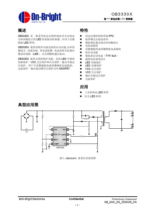
典型应用图
图 1: OB3330X 典型应用原理图
©On-Bright Electronics
Confidential -1-
Preliminary Datasheet OB_DOC_DS_3330X00_CN
OB3330X
高 PF 原边反馈 LED 控制器
VCC欠压保护 VCC欠压保护功能具有迟滞控制。当VCC电压超过 15.2V阈值, 芯片启动正常工作; 当VCC电压低于9V 阈值, 芯片停止工作; 当VCC重新恢复到15.2V阈值, 芯片重新工作。
最大/最小导通时间 LED 恒流控制 OB3330X 采用原边反馈的恒流(CC)控制技术, 可以实现高精度的LED恒流输出。LED输出电流ILED 计算公式: 芯片的 LEB 时间决定最小导通时间(Typ. 300ns). 芯片限制的最大导通时间约为 50us。
ASTM_D3330中英文对照版

ASTM_D3330中英文对照版ASTM D3330中英文对照版Designation:D3330/D3330M–00名称:D3330/D3330M-00Standard Test Method for Peel Adhesion of Pressure-Sensitive Tape1压敏胶带剥离强度测试标准This standard is issued under the fixed designation D3330/D3330M;the number immediately following the designation indicates the year of original adoption or,in the case of revision,the year of last revision.A number in parentheses indicates the year of last reapproval.A superscript epsilon(e)indicates an editorial change since the last revision or reapproval.此标准是根据D3330/D3330M整理修订;名称后面的数字代表首发年份。
括号内为最近修订年份。
带有上标e表示最后一次发行或修订时的改动之处。
1.1.Scope1.1范围1.1.1These test methods cover the measurement of the peel adhesion of pressure-sensitive tapes.1.1.1这些测试方法主要是针对压敏胶带剥离强度的测试1.1.1.1Test Method A gives a measure of the adherence,when peeled at180°angle,to a standard steel panel or to other surface of interest for a single-coated tape.(加载板)1.1.1.1方法A是压敏胶带从一标准金属板180°剥离测试方法;------------2.1.1.2Test Method B gives a measure of the adherence to the backing of a single-coated tape.2.1.1.2方法B是测试单面背衬胶的粘性3.1.1.3Test Method C gives a measure of the adherence of double-coated tape to a standard steel panel or other surface of interest.3.1.1.3方法C是双面背衬胶与标准金属板的粘性测试方法;4.1.1.4Test Method D gives a measure of the adherence of the release liner to the adhesive of either single-or double-coated tape.4.1.1.4方法D是测试单面或者双面背衬胶离型纸的粘性5.1.1.5Test Method E gives a measure of the adherence of an adhesive transfer tape to a standard steel panel or other surface of interest.5.1.1.5方法E是测试无基材胶带与标准金属板之间的粘性6.1.1.6Test Method F gives a measure of the adherence,when peeled at90°angle,to a standard steel panel or other surface of interest for a single-coated tape.6.1.1.6方法F是测试胶带90°剥离方法;7.1.2These test methods provide a means of assessing the uniformity of the adhesion of a given type of pressure-sensitive adhesive tape.The assessment may be within a roll of tape,between rolls,or between production lots.7.1.2这些测试方法,是胶带的统一的评定方法;----------8.1.3Variations in either the tape backing or the adhesive,or both,affect the response.Therefore,these test methods cannot be used to pinpoint the specific cause(s)of non-uniformity.9.1.4These test methods may not be appropriate to test tapes having relatively stiff backings,stiff liners,or backings showing high stretch at low forces.These characteristics will result in a high variability for the test response which is not a true indication of the real nature of the adhesive bond.10.1.5Values stated in either SI or inch-pound units are to be regarded separately as standard.The values stated in each system may not be exact equivalents,therefore,each system must be used independently without combining values in any way.11.1.6These test methods are intended to replace AFERA4001,EN1939,PSTC-1,PSTC-2,PSTC-3and PSTC-4.1.7This standard does not purport to address all of the1These test methods are under the jurisdiction of ASTM Committee D-10on Packaging and are the direct responsibility of Subcommittee D10.14on Tape and Labels.Current edition approved Oct.10, 2000.Published December2000.Originally published as D3330–/doc/7f650282.html,st previous edition D3330/D3330M–99.Copyright. ASTM,100Barr Harbor Drive,West Conshohocken,PA19428-2959,United States.safety concerns,if any,associated with its use.It is the responsibility of the user of this standard to establish appropriate safety and health practices and determine the applicability of regulatory limitations prior to use.2.Referenced Documents2.1ASTM Standards:A666Specification for Austenitic Stainless Steel,Sheet,Strip,Plate and Flat Bar2D996Terminology of Packaging and Distribution Environments3D3715/D3715M Practice for Quality Assurance of Pressure-Sensitive Tapes3D 4332Practice for Conditioning Containers,Packages or Packaging Components for T esting3D5750Guide for Width and Lengths of Pressure-Sensitive Tape3E122Practice for Choice of Sample Size to Estimate a Measure of Quality for a Lot or Process42.2AFERA Standard:54001Self adhesive tapes–Measurementof peel adhesion2.3European Norm:6EN1939Self adhesive tapes–Measurement of peel adhesion from stainless steel or from its own backing 2.4Pressure Sensitive Tape Council Standards:7PSTC-1Peel Adhesion of Single Coated Pressure-Sensitive Tapes at180°Angle PSTC-2Peel Adhesion for Single Coated Pressure-Sensitive Tapes at90°Angle PSTC-3Peel Adhesion of DoubleCoated Pressure-Sensitive Tapes at180°Angle PSTC-4Adhesion to Liner of Presure-Sensitive Tapes at180°Angle1.3.Terminology2.3.1Definitions—T erminology found in Terminology D996shall apply.2Annual Book of ASTM Standards,Vol01.03.3Annual Book of ASTM Standards,Vol15.09.4Annual Book of ASTM Standards,Vol14.02.5Association des Fabricants Européens deRubans Auto Adhesifs(AFERA),LAM,Laan Copes van Cattenburch79,NL-2858EW,The Hauge,Netherlands.6European Norm,(EN);available from ComitéEuropéen de Normalisation(CEN),Rue deStassart,36,B-1050,Brussels,Belgium.7Pressure Sensitive Tape Council(PSTC),400North Michigan Ave.,#2200,Chicago,IL60611–4267.1.4.Summary of Test Method测试方法概要2.4.1Test Method A—Single-Coated Tapes,Peel Adhesion at180°Angle—A strip of tape is applied to a standard test panel(or other surface of interest)with controlled pressure.The tape is peeled from t he panel at180°angle at a specified rate,during which time the force required to effect peel ismeasured.方法A是压敏胶带的180°剥离。
伟迪捷3330操作说明书

操作说明书AL-75075Index: AA [ZH_S], 2013 年 9 月Videojet 3130/3330原版操作说明书译稿版权所有 2013,Videojet Technologies Inc.(下文简称为 Videojet)保留所有权利。
本 Videojet Technologies Inc. 文件包含受版权保护的机密信息,所有权归 Videojet 所有。
未经Videojet 事先批准,禁止复制、使用或公布本文件。
Videojet Technologies Inc.1500 Mittel Boulevard Wood Dale, IL 60191-1073 USA 电话(美国):传真(美国):传真:1-800-843-36101-800-582-1343630-616-3629分公司 - 美国:亚特兰大、芝加哥、洛杉矶、费城全球网络:加拿大、法国、德国、爱尔兰、日本、西班牙、新加坡、荷兰、英国全球分销商目录1前言 (5)2安全须知 (7)2.1使用的概念 (7)2.2激光等级 (7)2.3正确使用 (8)2.4保养和维修 (9)2.5保护和警告装置 (10)2.6对眼睛和皮肤的危害 (10)2.7设置/更改标记区域 (11)2.8硒化锌透镜的安全信息 (11)2.9存在燃烧爆炸危险 (12)2.10电气安全 (12)2.11分解物 (13)2.12警告和提示牌 (13)3调试 (15)3.1安装和调试 (15)3.2运输和存放 (15)3.3开箱 (16)3.4安装条件 (16)3.5冷却装置 (18)3.6抽吸装置 (18)3.7激光系统的接口 (18)3.8硬件和软件要求 (19)3.9安装软件 (19)3.10确定 IP 地址 (19)3.11停机 (20)3.11.1暂时停机 (20)3.11.2最终停机 (20)4系统描述 (21)4.1矢量扫描激光系统的功能原理 (21)4.2激光射线源 (21)4.3打标头 (21)4.4标记产品表面 (22)4.5激光参数 (22)4.6激光系统的构造 (22)4.7技术数据 (23)4.8工作距离和标记区 (24)5激光系统的操作 (27)5.1激光系统的操作 (27)5.2标记模板的组成部分 (27)5.3供应单元上的元件 (28)5.4激光系统运行状态 (29)5.5开启/关闭供应单元 (30)6保养 (31)6.1保养说明 (31)6.2保养计划 (31)6.3清洁聚焦光学器件 (31)6.3.1拆卸聚焦光学器件 (32)6.3.2清洁聚焦光学器件 (32)6.3.3安装聚焦光学器件 (33)6.4更新软件 (33)6.5保养、维修和更换记录 (33)7故障 (40)7.1提示 (40)7.2故障描述 (40)8附录 (42)8.1ACC 上的用户接口分配 (42)8.1.1内锁 (42)8.1.2电气隔离的输入端和输出端 (42)8.1.3未电气隔离的输入端 (44)8.2布线示例 (45)8.2.1布线示例 2:直接连接 (MOTF mark on the fly) (45)8.2.2布线示例 1:通过 PLC 控制 (46)8.2.3布线示例 3:任务选择 (47)8.2.4布线示例 4:内部安全模块 (47)8.2.5布线示例 5:外部安全模块 (48)8.3图纸 (49)8.4硒化锌 (ZnSe) 安全数据表 (54)8.5缩写 (57)索引 (58)1 前言本操作说明书......包含用于确保正常运行、排除微小故障以及维护激光系统所需的全部信息。
ASTMD3330剥离强度测试标准中文版

压敏胶带剥离强度测试标准1、范围1。
1 这些测试方法主要用于压敏胶带剥离强度得测试、1。
1。
1ﻩ方法 A:单面胶从标准钢板或其她类似表面得平板上180°剥离得测试方法。
1、1。
2ﻩ方法B:单面背衬胶粘性得测试方法。
1.1。
3ﻩ方法C:双面胶与标准钢板粘性得测试方法。
1、1.4 方法D:单面胶或双面胶与离型纸得粘性得测试方法。
1.1。
5方法E:无基材胶带与标准钢板得粘性得测试方法。
1。
1。
6 方法F:单面胶与标准钢板90°剥离得测试方法、1。
2 这些测试方法就是给定压敏胶带粘性测试得统一评定方法,这评定可以针对一卷,两卷之间或一批。
1、3 不同得基材与(或)胶质都会影响测定结果,因此,这些方法不适用不统一得胶质。
1.4 这些测试方法不适用于一些相对硬质得基材、衬里或在低强度下高粘性背胶得测试、这些特性对测试结果有很大得影响,因而不能真正代表粘力。
1.5测试数值用 IS 或英寸—磅做为单位,在每个单位系统中数值得规定都就是不同得,因此,每个系统必须使用自己得单位、1。
6这些标准没用强调在操作过程中可能会发生得所有安全隐患。
标准使用者有义务去建立一个安全健康得操纵规则。
4、测试方法概要4、1 方法 A-—单面胶180°剥离-—用可控压力把胶带粘贴到标准测试板上、测试时,以恒定得速度180°角从测试板上剥离。
4、2 方法B——单面背衬胶得粘性——胶带式样一粘贴到测试钢板上, 取另一式样粘贴到式样以得背面,然后按方法 A 进行测试。
4。
3方法C——双面胶4、3.1 表面粘性-—把双面胶得正面贴到不锈钢板上,衬里面朝外。
撕去衬纸,贴一层0、025mm(0.001in)得聚酯薄膜,接下来按方法A 进行测试。
4、3.2ﻩ衬里粘力——在双面胶得正面贴上0.025mm 得聚酯薄膜,然后撕去衬纸贴到不锈钢板上。
接下来得测试同方法A。
4.4 方法 D-—测试离型纸胶带(单面或者双面)得粘性——把胶带粘贴到测试钢板上,衬里面朝外。
Seagate双面USB3.0保护盘驱动器说明草稿说明书

DESKTOP DRIVE WITH INTEGRATEDUSB HUBData SheetEasy backup with integrated USB 3.0 hub to manageand charge your devicesThe Seagate® Backup Plus Hub drive optimises external storage withsimple file backup for your computers — and an intelligent USB hub tocharge and manage your USB-connected devices.High-speed USB 3.0 and 2.0 connectivity offers plug-and-playfunctionality on your PC. The drive is formatted for Windows computers.Install the provided NTFS driver for Mac® on your Mac computer, and youcan use the drive interchangeably between Windows and Mac computerswithout reformatting.1The two front-facing intelligent USB 3.0 ports amplify the functionality ofyour drive by allowing you to charge and connect two external devices,like your phone, tablet or camera — even if your computer is inoff/standby mode.Back up your favourite files, photos and video from your PC usingdownloadable Seagate backup software. Run a one-click backup orschedule an automatic backup plan to protect your files in your BackupPlus Hub drive at your convenience.1 Requires formatting for Time Machine backup.DESKTOP DRIVE WITH INTEGRATED USB HUBSpecificationsRetail Packaging Product Dimensions Pallet Dimensions Length (in/mm) 4.646 in/118 mm40 in/1,016 mm Width (in/mm) 1.614 in/41 mm47.992 in/1,219 mm Depth (in/mm)7.799 in/198.1 mm45.157 in/1,147 mm Weight (lb/kg) 2.341 lb/1.062 kg996.578 lb/452.04 kg QuantitiesBoxes per Master Carton4Master Cartons per Pallet644 month membership to Adobe Photography Creative Cloud plan4。
ob3330cp开关电源原理分析

ob3330cp开关电源原理分析
开关电源就是用通过电路控制开关管进行高速的导通与截止。
将直流电转化为高频率的交流电提供给变压器进行变压,从而产生所需要的一组或多组电压!转为高频交流电的原因是高频交流在变压器变压电路中的效率要比50HZ高很多.所以开关变压器可以做的很小,而且工作时不是很热!成本很低.如果不将50HZ变为高频那开关电源就没有意义。
开关电源的工作流程是:电源→输入滤波器→全桥整流→直流滤波→开关管(振荡逆变)→开关变压器→输出整流与滤波。
通过高频PWM(脉冲宽度调制)信号控制开关管,将那个直流加到开关变压器初级上开关变压器次级感应出高频电压,经整流滤波供给负载输出部分通过一定的电路反馈给控制电路,控制PWM占空比,以达到稳定输出的目的:交流电源输入时一般要经过厄流圈一类的东西,过滤掉电网上的干扰,同时也过滤掉电源对电网的干扰;在功率相同时,开关频率越高,开关变压器的体积就越小,但对开关管的要求就越高;开关变压器的次级可以有多个绕组或一个绕组有多个抽头,以得到需要的输出;一般还应该增加一些保护电路,比如空载、短路等保护,否则可能会烧毁开关电源。
海斯特重型货车胎型磨枕H300-360XD系列产品说明书

in mm
100
2,540
4-22 Fork dimension
in mm
3.5/8/48
90/200/1,220
4-23 Fork carriage type
Type
Standard pin type carriage
4-24 Carriage width
in mm
98.3
2,496
4-25-1 Fork spread, min (in-in)
33/29
38/29
Cummins QSB 6.7L
17
18
27
29
-
-
71
79 0.36 0.40
-
-
106 94 0.54 0.48
20,700 21,900 92
97
23,400 24,900 104 111
31/29
36/29
75
1,902
268
6,812
196
4,983
100
2,540
3.5/8/48
98
5-6 Drawbar pull - stall, with/without load
lb kN 23,500 24,700 105 110
5-7 Gradeability - 1 mph (1.6 km/h), with/without load
%
33/31
5-8 Gradeability stall, with load/without load
#
x4/2
3-6 Tread width, front
in mm
72.5
1,842
3-7 Tread width, rear
Omega PX2310 Series产品说明书

PX2310 SERIES M-5260/0213OMEGAnet Online Service Internet e-mail **************Servicing North America:U.S.A: Omega Engineering, Inc., One Omega Drive, P .O. Box 4047ISO 9001 Certified Stamford, CT 06907-0047 USA Toll Free: 1-800-826-6342 TEL: (203) 359-1660 FAX: (203) 359-7700 email: **************Canada: 976 Bergar Laval (Quebec), Canada H7L 5A1 Toll Free: 1-800-826-6342 (514) 856-6928 FAX: (514) 856-6886 email: **************For immediate technical or application assistance:U.S.A and Canada: Sales Service: 1-800-826-6342/1-800-TC-OMEGA® Customer Service: 1-800-622-2378/1-800-622-BEST® Engineering Service: 1-800-872-9436/1-800-USA-WHEN®Mexico: En Español: 001 (203) 359-7803 FAX: (001) 203-359-7807**************.mx e-mail: *****************Servicing Europe:Benelux: Managed by the United Kingdom Office Toll-Free: 0800 099 3344 TEL: +31 20 347 21 21FAX: +31 20 643 46 43 e-mail:**************France: Managed by the United Kingdom Office Toll-Free: 0800 466 342 TEL: +33 (0) 161 37 29 00 FAX: +33 (0) 130 57 54 27 e-mail:**************Germany/Austria: Daimlerstrasse 26 D-75392 Deckenpfronn, Germany Toll-Free************ TEL: +49 (0) 7059 9398-0 FAX: +49 (0) 7056 9398-29e-mail:*************United Kingdom: OMEGA Engineering Ltd.ISO 9001 Certified One Omega Drive, River Bend Technology Centre, Northbank Irlam, Manchester M44 5BD England Toll-Free: 0800-488-488 TEL: +44 (0)161 777-6611 FAX: +44 (0)161 777-6622 e-mail:**************.uk ®It is the policy of OMEGA Engineering, Inc. to comply with all worldwide safety and EMC/EMI regulations that apply. OMEGA is constantly pursuing certification of its products to the European New Approach Directives. OMEGA will add the CE mark to every appropriate device upon certification.The information contained in this document is believed to be correct, but OMEGA accepts no liability for any errors it contains, and reserves the right to alter specifications without notice.W ARNING: These products are not designed for use in, and should not be used for, human applications.Contents1.0 GENERAL INFORMATION2.0 MECHANICAL INSTALLATION2.1 Medial Compatibility2.2 Environment2.3 Pressure Fittings2.4 Mounting2.5 Installation Procedures3.0 OPTIONAL 3-VALVE MANIFOLD PROCEDURE4.0 ELECTRICAL INSTALLATION4.1 Electrical TerminationWiring: 2-Wire, 4 to 20 mA and Remote Zero4.2 Electrical TerminationWiring: 3-Wire, 0 to 5, 0 to 10 VDC and Remote Zero5.0 OPERATION6.0 RETURNING PRODUCTS FOR REPAIRInstallation GuideMulti-Sense PX2310 SeriesWet-to-Wet Differential Pressure Transducers1.0 GENERAL INFORMATIONEvery PX2310 has been calibrated and tested before shipment to guarantee performance of all pres-sure ranges.The PX2310 has field selectable unidirectional and bidirectional pressure ranges, configurable 0 to 5 VDC, 0 to 10 VDC, and 1 to 5 VDC output, true two wire 4 to 20 mA, and auto-zero capability. The PX2310 is factory calibrated to the highest pressure range. The range label on the side of the unit indicates the factory calibrated range.Omega PX2310 pressure transducers sense differential pressure and convert difference in overpres-sure to a proportional high level analog output for unidirectional and bidirectional pressure ranges.Your PX2310 Multi-Sense pressure transducer has been ordered in one of the following versions: Version Unidirectional Bidirectional PX2310 050 DX5, 10, 20, 50 psid±5, ±10, ±20, ±50 psidPX2310 100 DX10, 20, 50, 100 psid±10, ±20, ±50, ±100 psidPX2310 250 DX25, 50, 125, 250 psid±25, ±50, ±125, ±250 psid2.0 MECHANICAL INSTALLATION2.1 Media CompatibilityPX2310 transducers are designed to be used with any gas or liquid compatible with 17-4 PH stainless steel. The optional 3-valve manifold assembly is designed to be used with gases or liquids compat-ible with 360 Brass, Acetal plug valves and Nitrile O-Rings. Never totally submerge the unit in any liquid.2.2 EnvironmentThe operating temperature limits of the PX2310 are as follows:Compensated Temperature Range °F (°C)+32 to +130 (0 to +54)Operating Temperature Range °F (°C)-4 to +185 (-20 to +85)Storage Temperature Range °F (°C)-4 to +185 (-20 to +85)2.3 Pressure Fittings Typically standard pipe fittings and installation procedures should be used.The PX2310 has 1/8” -NPTF internal fittings. The high pressure port and low pressure port are locat -ed on the bottom of the unit, labeled “HI” and “LO”, respectively The optional 3-valve manifold as-sembly with the 1/4” -18NPT internal fittings.Moisture PrecautionsThe PX2310 is provided with a 0.875 DIA. conduit opening for electrical termination, intended for a 1/2” I.D. conduit connection. The opening must be sealed according to standard industry practices in order to prevent moisture ingress into the PX2310.2.4 Mounting The PX2310 can be easily mounted using the two mounting screws located on the side of the unit.2.5 Installation Procedures If the PX2310 is supplied with an optional 3-valve Manifold assembly, refer to section3.0, Optional 3-Valve Manifold Assembly Procedure, for further installation procedures. If the PX2310 is not sup-plied with a Omega 3-Valve manifold, the following installation procedure is recommended.For differential pressure measurements at high line pressure, it is recommended that the pressure sensor be installed with a valve in each line, plus a shunt valve across the high and low (reference) pressure ports as shown.FIGURE 1:Important: Do not exceed maximum range pressure with the total of differential pressure and line pressure.FIGURE 2:3.0 OPTIONAL 3-VALVE MANIFOLD PROCEDUREThe 3-Valve Manifold Assembly is normally shipped with valves V1 and V2 closed and V3 open. To Place the PX2310 into service:1. Confirm valves V1 and V2 are closed and valve V3 is open2. Mount the manifold and install process connections3. Slowly open V2, then V14. Close the V3 valve.To Take the PX2310 out of service:1. Open V3 to equalize the pressure at the PX23102. Close the V2 and V2 valves.PX2310 - Outline DrawingFIGURE 3:4.0 ELECTRICAL INSTALLATIONTo access the electrical connections, turn the screws on the top of the case counter clockwise until the hinged cover can be flipped up. The screws are captured and secured in the cover. Wiring is through the 1/2” conduit opening. Both current and voltage outputs are reverse wiring protected.Note: The Zero terminals, connected to digital output, provide a contact closure relay for automatic reset to zero pressure by the monitoring system. CAUTION: ZERO input is for dry contact, do not apply voltage to ZERO Terminals.4.1 Electrical TerminationWiring: 2-Wire - 4 to mA (Current Output) and Remote ZeroPX2310 when configured as a current output transducer is a true 2-wire, 4-20 mA current output de-vice and delivers rated current into any external load of 0-1000 ohms.When configured as a 4-20 mA current output device the current flow is in one direction only. PLEASE OBSERVE POLARITY.We suggest that an electrical cable shield be connected to the system’s loop circuit ground to improve electrical noise rejection.Min. Supply Voltage:12 + .02 x (Resistance of receiver plus line) Max Supply Voltage:30 + .004 x (Resistance of receiver plus line) The optional remote zero is normally open relay wired between COM and REMOTE ZERO terminals. In order to initiate ZERO function the relay contact shall be closed.FIGURE 4:050 DX100 DX250 DX4.2 Electrical Termination Wiring: 3-Wire, 0 to 5, 0 to 10, 1-5 VDC and Remote ZeroThe PX2310 when configured for voltage output is a 3-wire circuit device with three terminals avail -able for wiring. The -Excitation and -Output are commoned on the circuit.The PX2310 can operate from 12-30 VDC (18-28 VAC) nominal output power supply.Note: The Zero terminals, connected to digital output, provide a contact closure relay for automatic reset to zero pressure by the monitoring system. CAUTION: ZERO input is for dry contact, do not apply voltage to ZERO Terminals.The optional remote zero is a normally open relay wired between COM and REMOTE ZERO termi-nals. In order to initiate ZERO function in the relay contact shall be closed.FIGURE 5:Installation of the PX2310 is not complete.Important: Prior to putting the unit into service, press the “Zero” button, then use the “Range Selection Switch” to select a range. After selecting a range, press the “Zero” button again. For instructions regarding operation of the PX2310, please refer to Section 5.050 DX100 DX250 DX5.0 OPERATIONFIGURE 6:Range Selection Switch: The unit is set to the highest range when calibrated at the factory. To select the other ranges, slide the switch to the right. Important: Push “zero” button after installing the PX2310, and after changing range.Auto Zero Button: Press and hold the “ZERO” push-button for 2 seconds to automatically reset zero or provide contact closure on “Remote Zero, see figure 4 and figure 5.Electrical Output: The unit is set at the factory to 4-20 mA. To select another output, move the slide switch to the right.Electrical Connections: Electrical termination for power supply, 3-wire voltage output and 2-wire true 4-20 mA current output, and remote zero wiring.A.REV/NORM:A.REV: Analog Revers: When in reverse mode, the output increases when the differential pressure decreases and decreases as pressure increases.NORM: When in Normal mode output increases as pressure increases and decreases as pressure decreases.SLOW/FAST: When Slow mode is selected, 5-second averaging is provided for surge daming.BI-DIR/UNI-DIR: Select UNI-Directional or BI-Directional mode.Unidirectional mode measures from 0 to full scale differential pressure.Bidirectional mode measures pressure from minus 1/2 of full scale to plus 1/2 of full scale to differen-tial pressure. Output with read 1/2 full scale when differential pressure is zero.SWAP/NORM: Jumper selectable Port Swap feature eliminates costly replumbing when incorrectly installed or replaced. Go from NORMAL to SWAP and the jumper makes the “HI” and the “LO” port “HI”050 DX 100 DX250 DX6.0 RETURNING PRODUCTS FOR REPAIRPlease contact Omega at 1-800-826-6342 or 1-203-359-1660 before returning unit for repair to review information relative to your application. Many times, only minor field adjustments may be necessary. When returning a product to Omega, the material should be carefully packaged and shipped prepaid to:Omega Engineering, IncOne Omega DriveP.O. Box 4047Stamford, CT 06907-0047To assure prompt handling, please supply the following information and include it inside the package of returned material:1. Name and phone number of person to contact.2. Shipping and billing instruction.3. Full description of the malfunction.4. Identify any hazardous material used with product.Notes: Please remove any pressure fittings and plumbing that you have installed and enclose any re-quired mating electrical connectors and wiring diagrams. Allow approximately 3 weeks after receipt at Omega for the repair and return of the unit. Non-warranty repairs will not be made without customer approval and a purchase order to cover the repair charges.Calibration ServicesOmega maintains a complete calibration facility that is traceable to the National Institute of Standards & Technology (NIST). If you would like to recalibrate or re-certify your Omega pressure transducers or transmitters, please call our Sales Department at 1-800-826-6342 or 1-203-359-1660 for scheduling, cost and turnaround estimates.Thank you,Omega Engineering, Inc.OMEGA ENGINEERING, INC. warrants this unit to be free of defects in materials and workmanship for a period of 13 months from date of purchase. OMEGA’s WARRANTY adds an additional one (1) month grace period to the normal one (1) year product warranty to cover handling and shipping time. This ensures that OMEGA’s customers receive maximum coverage on each product.If the unit malfunctions, it must be returned to the factory for evaluation. OMEGA’s Customer Service Department will issue an Authorized Return (AR) number immediately upon phone or written request. Upon examination by OMEGA, if the unit is found to be defective, it will be repaired or replaced at no charge. OMEGA’s WARRANTY does not apply to defects resulting from any action of the purchaser, including but not limited to mishandling, improper interfac-ing, operation outside of design limits, improper repair, or unauthorized modification. This WARRANTY is VOID if the unit shows evidence of having been tampered with or shows evidence of having been damaged as a result of excessive cor-rosion; or current, heat, moisture or vibration; improper specification; misapplication; misuse or other operating conditions outside of OMEGA’s control. Components in which wear is not warranted, include but are not limited to contact points, fuses, and triacs.OMEGA is pleased to offer suggestions on the use of its various products. However, OMEGA neither assumes responsibility for any omissions or errors nor assumes liability for any damages that result from the use of its products in accordance with information provided by OMEGA, either verbal or written. OMEGA warrants only that the parts manufactured by the company will be as specified and free of defects. OMEGA MAKES NO OTHER WARRANTIES OR REPRESENTATIONS OF ANY KIND WHATSOEVER, EXPRESSED OR IMPLIED, EXCEPT THAT OF TITLE, AND ALL IMPLIED WARRANTIES INCLUDING ANY WARRANTY OF MERCHANTABILITY AND FITNESS FOR A PARTICULAR PURPOSE ARE HEREBY DISCLAIMED. LIMITATION OF LIABILITY: The remedies of purchas -er set forth herein are exclusive, and the total liability of OMEGA with respect to this order, whether based on contract, warranty, negligence, indemnification, strict liability or otherwise, shall not exceed the purchase price of the component upon which liability is based. In no event shall OMEGA be liable for consequential, incidental or special damages.CONDITIONS: Equipment sold by OMEGA is not intended to be used, nor shall it be used: (1) as a “Basic Component” under 10 CFR 21 (NRC), used in or with any nuclear installation or activity; or (2) in medical applications or used on hu-mans. Should any Product(s) be used in or with any nuclear installation or activity, medical application, used on humans, or misused in any way, OMEGA assumes no responsibility as set forth in our basic WARRANTY/DISCLAIMER language, and, additionally, purchaser will indemnify OMEGA and hold OMEGA harmless from any liability or damage whatsoever arising out of the use of the Product(s) in such a manner.Direct all warranty and repair requests/inquiries to the OMEGA Customer Service Department. BEFORE RETURNING ANY PRODUCT(S) TO OMEGA, PURCHASER MUST OBTAIN AN AUTHORIZED RETURN (AR) NUMBER FROM OME-GA’S CUSTOMER SERVICE DEPARTMENT (IN ORDER TO AVOID PROCESSING DELAYS). The assigned AR number should then be marked on the outside of the return package and on any correspondence.The purchaser is responsible for shipping charges, freight, insurance and proper packaging to prevent breakage in transit.FOR WARRANTY RETURNS, please have the following information available BEFORE contacting OMEGA:1. Purchase Order number under which the product was PURCHASED,2. Model and serial number of the product under warranty, and 3. Repair instructions and/or specific problems relative to the product.OMEGA’s policy is to make running changes, not model changes, whenever an improvement is possible. This affords our customers the latest in technology and engineering.OMEGA is a registered trademark of OMEGA ENGINEERING, INC.© Copyright 2009 OMEGA ENGINEERING, INC. All rights reserved. This document may not be copied, photocopied,reproduced, translated, or reduced to any electronic medium or machine-readable form, in whole or in part, without the prior written consent of OMEGA ENGINEERING, INC.FOR NON-WARRANTY REPAIRS, consult OMEGA for current repair charges. Have the following information available BEFORE contacting OMEGA:1. Purchase Order number to cover the COST of the repair,2. Model and serial number of the product, and 3. Repair instructions and/or specific problems relative to the product.TEMPERATUREThermocouple, RTD & Thermistor Probes, Connectors, Panels & Assemblies Wire: Thermocouple, RTD & ThermistorCalibrators & Ice Point ReferencesR ecorders, Controllers & Process MonitorsInfrared PyrometersPRESSURE, STAIN AND FORCETransducers & Strain GagesLoad Cells & Pressure GagesDisplacement TransducersI nstrumentation & AccessoriesFLOW/LEVELRotameters, Gas Mass Flowmeters & Flow ComputersAir Velocity IndicatorsTurbine/Paddlewheel SystemsT otalizers & Batch ControllerspH/CONDUCTIVITYpH Electrodes, Testers & AccessoriesBenchtop/Laboratory MetersControllers, Calibrators, Simulators & PumpsI ndustrial pH & Conductivity EquipmentDATA ACQUISITIOND ata Acquisition & Engineering SoftwareCommunications-Based Acquisition SystemsPlug-in Cards for Apple, IBM & CompatiblesDatalogging SystemsRecorders, Printers & PlottersHEATERSHeating CableCartridge & Strip HeatersImmersion & Band HeatersF lexible HeatersLaboratory HeatersENVIRONMENTALMONITORING AND CONTROLMetering & Control InstrumentationRefractometersPumps & TubingAir, Soil & Water MonitorsIndustrial Water & Wastewater TreatmentpH, Conductivity & Dissolved Oxygen Instruments。
- 1、下载文档前请自行甄别文档内容的完整性,平台不提供额外的编辑、内容补充、找答案等附加服务。
- 2、"仅部分预览"的文档,不可在线预览部分如存在完整性等问题,可反馈申请退款(可完整预览的文档不适用该条件!)。
- 3、如文档侵犯您的权益,请联系客服反馈,我们会尽快为您处理(人工客服工作时间:9:00-18:30)。
-40
-10
20
50
80
110
140
Temperature(℃)
UVLO(ON) vs Temperature
10.5 10 UVLO(ON)(V) 9.5 9 8.5 8 -40 -10 20 50 UVLO(OFF)(V) 16.5 16
UVLO(OFF) vs Temperature
en fid
OB3330X
高 PF 原边反馈 LED 控制器
概述
OB3330X 是一款采用原边反馈控制技术并实现高 功率因数校正的 LED 恒流驱动控制器,应用于反激 隔离 LED 照明。 OB3330X 提供的特性功能包括软启动功能,功率因 数校正, 恒流控制, 零电流检测, 电流采样比较器内 置前沿消隐(LEB) ,以及图腾柱输出驱动。 OB3330X 提供全面的保护功能,包括 LED 开路和 短路保护,VCC 过压保护和欠压保护,输出负载过 压保护,用户可设置阈值的逐周期峰值电流限制, 过温保护,输出驱动钳位以保护功率 MOSFET。
应用
o
OB3330X
高 PF 原边反馈 LED 控制器
基本信息
引脚排布 SOP8 引脚图如下
ZCD 1 8 VCC
额定封装散热 封装 SOP8
RθJA (℃/W) 150
应用极限参数 参数 VCC输入电压到地 GATE到地3 ZCD 到地 3 OCP_TH, MULT, COMP, 以及 CS 到地 工作环境温度 TA 最小/最大工作结温TJ 最小/最大储藏温度Tstg 管脚焊接温度(10secs) 范围 -0.3V to 40V -0.7V to 40V -1V to 7V -0.7V to 7V -20℃ ~ 85℃ -40 ~150℃ -55 ~150℃ 260 ℃
Vref Iref
ZCD
Vth_ovp
+ _
Vth_zcd
Logic Control
Gate Drive
GATE
OCP_TH
OCP PWM
MULT Multiplier
tia
lt
Constant Current Regulation
o
CS
fid
COMP
en
GND
O n-
Br ig
©On-Bright Electronics Confidential -4-
O n-
Br ig
©On-Bright Electronics
ht c
on
fid
Confidential
lt
Preliminary Datasheet OB_DOC_DS_3330X00_CN
o
OB3330X
高 PF 原边反馈 LED 控制器
功能方框图
VCC
OTP
UVLO
Voltage & Current Reference
ht c
on
图 2: OB3330X 功能方框图
Preliminary Datasheet OB_DOC_DS_3330X00_CN
OB3330X
高 PF 原边反馈 LED 控制器
电气参数
(如无特殊说明,环境温度 TA = 25℃, VCC=16V)
符号 电源电压 I_VCC_ST I_static UVLO(ON) UVLO(OFF) VCC_OVP 电流反馈 T_leb Td_oc IOCP_TH Vth_OCP 乘法器 Vmult K 零电流检测 Vovp Vth_dem_H Vth_dem_L 恒流控制 Vref Gm Gain Vcomp_h Vcomp_l Isource_max Isink_max Toff_max Ton_max 过温保护 OTP_on Vol Voh Vclamp Tr Tf 输入工作电压范围 乘法器 DC 增益 COMP=3V 参数描述 测试条件 VCC=14V VCC=16V, no switching VCC falling VCC rising 8 14.2 最小值 典型值 5 1.5 9 15.2 30 300 From OCP comparator to Gate drive VCC=16V 0V<VOCP_TH<0.3V 0.3V<VOCP_TH<1.5V VOCP_TH>1.5V 17 100 28 2.1 1.8 1.5 0 0.91 3.75 4 0.9 0.3 392 60 400 80 70 6 1.2 32 100 55 50 408 4.25 3 39 最大值 15 2.5 10 16.2 单位 uA mA V V V nS nS uA V V V V 1/V V V V mV uS dB V V uA uA us us
启动电流 工作电流 VCC 欠压保护(ON)阈值 VCC 欠压保护(OFF)阈值 VCC 过压保护阈值 前沿消隐时间 芯片传输延迟
OCP_TH 引脚的上拉电流 可设置的 OCP 阈值
MULT=1V, COMP=3.5V
输出过压保护阈值
退磁计时开始 ZCD 阈值 退磁计时结束 ZCD 阈值 EA 参考电压 EA 跨导增益 EA DC 增益
VCC欠压保护 VCC欠压保护功能具有迟滞控制。当VCC电压超过 15.2V阈值, 芯片启动正常工作; 当VCC电压低于9V 阈值, 芯片停止工作; 当VCC重新恢复到15.2V阈值, 芯片重新工作。
en
-7-
LED 恒流控制
fid
on
OB3330X 采用原边反馈的恒流(CC)控制技术, 可以实现高精度的LED恒流输出。LED输出电流ILED 计算公式:
OB3330X
高 PF 原边反馈 LED 控制器
标识信息
YWWZZZ OB3330CP
X s
Y: Year Code WW: Week Code (01-52) ZZZ:Lot Code C: SOP8 P:Pb-free Package S: Internal Code(Optional)
引脚说明
80 110 140
tia
lt
15.5 15 14.5 14 -40 -10 20 50 80 110 140 Temperature(℃) Temperature(℃)
I_VCC_ST vs Temperature
on
o
1.8 1.5 1.2 Vcs(V) 0.9 0.6 0.3
Vcs vs Vmult
ht c
N 400[mV ] I LED [mA] 2 RCS []
Br ig
N—原边绕组和副边绕组匝比
Rcs—连接MOSFET源极和地的采样电阻
O n-
电流采样
OB3330X 提供逐周期的电流限制(OCP),通过 CS 引脚检测接至其引脚采样电阻 (Rcs) 上的开关电流 大 小 。 Snubber 二 极 管 的 反 向 恢 复 特 性 导 致 MOSFET 开通瞬间在采样电阻上产生尖峰电压, 芯 片内置前沿消隐电路可以屏蔽该尖峰电压,因此在 电流检测输入端无需外接 RC 滤波电路。在该屏蔽 时间内电流限制比较器不会工作,因此外部 MOSFET 不会关闭。 电流采样的输入电压和 COMP 电压决定 PWM 占空比
启动 OB3330X优化设计了启动电流 (Typ. 5uA) , 当VCC 电压经启动电阻充电高于UVLO(OFF)阈值电压, 芯片可以很快开启工作,因此在系统板上可以使用 高阻值的启动电阻来减小功率损耗。
零电流检测 OB3330X 的 ZCD 引脚连接到辅助绕组的电阻分压 节点,监测辅助绕组电压实现零电流检测。ZCD 引 脚电压反映反激变压器极性的变化。当存储于反激 变压器中的能量传输到输出并完全释放完毕,对应 ZCD 引脚上的电压下降。当 ZCD 引脚上的电压下 降到 0.3V 阈值,触发内部的 ZCD 比较器并产生新 的 PWM 开关周期。
OCP_TH 引脚电压决定 OCP 阈值。OB3330X 的 OCP_TH 引脚提供约 28uA 充电电流。为了产生 OCP_TH 引脚所需的电压,OCP_TH 需要连接合 适的电阻到地。 当 OCP_TH 引脚接 33kΩ 电阻到地, OCP 阈值约为 1.8V; 当 OCP_TH 引脚接 110kΩ 电 阻到地, OCP 阈值约为 1.5V;当 OCP_TH 引脚接 地, OCP 阈值约为 2.1V。 OCP_TH 引脚 电压(V) 3 0.9 0 OCP_TH 连接 的电阻(kΩ) 110 33 0 OCP 阈值 (V) 1.5 1.8 2.1
O n-
Br ig
脉冲宽度调制
ht c
最高钳位电压 最低钳位电压
EA 最大充电电流 EA 最大放电电流 最大关断时间 最大导通时间
过温保护阈值
on
fid
en
tia
lt
o
145 VCC=16V@ Iout=100mA VCC=16V@ Iout=100mA Vcc=28V CL=1nF, 10~90% CL=1nF, 10~90% 8 11 80 30 12.5 150 70 1.5
特性
原边反馈控制的单级 PFC 临界模式实现高效率 模拟乘法器实现功率因数校正 高恒流精度 设置阈值的逐周期峰值电流限制 软启动功能 极低的启动电流(TYP. 5uA) 最简化的系统设计 LED 开路保护 LED 短路保护 VCC 过压保护 VCC 欠压保护 输出负载过压保护 过温保护
高 PF 原边反馈 LED 控制器
特征曲线图
I_static vs Temperature
3.5 3 I_static(mA)
Vref vs Temperature
415 410 405 Vref(mV) 400 395 390 385 380
2.5 2 1.5 -40 -10 20 50 80 110 140 Temperature(℃)