KT6008-1A升压型DC-DC芯片
LTC3108:升压型DC/DC转换器
(6 A 和 高效率设计确保了尽可能快 的充电时间,旨在满 < p)
足 输出 存储电 容器的 需要。 圈 匿囡
Li ear w ww. nea . n 1 i rcom . cn
度传感器 输入以 监察过热故障。
瞄团圃
AUIS7 1 / 1 智 能功 率 开 关 P 1 1 2 R 4 R:
的汽车质 量理念下研制而成 的,所 采用的环保材料既不含
D 14 工作在 .0 S 2 8 4 ℃至 + 5 扩展级温度范围,提供 8o c
带有裸焊盘的小尺寸 3 mm、1 mm X3 4引脚 T N封装。 DF
Ma m xi ¨ n m 力-c c ,.伽
铅, 合有害物 也符 质管 制指令(o S 。 豳 R l ) 匿回
温度范围内提供 +- % 的精确 电流反馈 ,并能通过优化开 D /5 C控 制器 配合 工作 ,构
关时间将易受电磁干扰的汽车应用的噪声降至最低。
建 DC D / C升压转换器 。D
新器件均符合 A C Q1 0标 准,是在 l E — 0 R要求 零缺陷 OL T中的 AP D偏置和电流监测 。
确保开关安全可靠 。此外 ,新器 件的过流关断 、过温关断 集成 高压 (6 电流源和 7 V) 和有 源箝 位电路功能都能确保在短路 的情 况下实现安全运 双电流镜 ,用于监测 A D P 行和保护 。
电流。该器件还 包含一个
除了众多保护功能 ,A IS 1X UP 7 系列还 可在整4I作 F T开 关 ,可 与外 部 D I X " E C
41 .V或 5 固定 电压 中选 择一个 ,为无 线发送器 或传感 冗余电路的可靠设计。 V)
器供 电。第二个 开关输 出可 由主器件 启动 ,为没有微功率 停机功能 的器件供 电。甚至在输入能源无 法得到时 ,增加
必能信 8700超音波使用手册

2 8700 ADVANCED 塑焊系统的安装
2.1 安装要求 ································································································ 2-1 2.1.1 安装空间 ······················································································ 2-1 2.1.2 环境要求 ······················································································ 2-3 2.1.3 电源输入范围 ·············································································· 2-3 2.1.4 工厂气源 ······················································································ 2-3 2.1.5 气源输入接口 ·············································································· 2-4
创维电视维修经验荟萃大全

5D60
首次开机黑或灰屏,或 开机慢,二次开机正常
将R904、R905由2.7Ω/3W改为1Ω /3W(短路此二电阻可改善开机慢) 或更换C951
更换高频头(由18改为28),如出
408.25MHz、456.25MHz 现较多的重台或假台,须更改数
收不到台
据:19FH:14H或17H或20-22H,
音量在“10”以下时能听 消磁线圈离电子重低音距离近造成
到明显的“嗡嗡”声 的
图闪
CRT板上G2点的焊线过长引起对地 打火
增强逐行DVD效果
将主板上J724由100Ω/0.25W改为 470Ω/0.25W。
将信号板CN450与电源板CN401之间
音量调到“0”或“1”时 的连线尽量前移压到主板支架的下
100---2982接收当地有 线,收不到中央八套, 手动、微调均调不出。 (该台在当地增补频道 104.25MHz)
1):将频道号打到101(此时显示 为113MHz)。 2):进入“微调”项,按音量减调 出图像(104.25MHz)。 3):进入“存台”项,按音量-/+ 键,保存该节目。
100--2982接收图象时,
--1200欧。
2982---100重低音干扰 (参看《维修通讯》合 订本158页)
方案一:将C432、C433由跨接线改 为10µF/50V电容,将C432、C433负 极短接,背面补加一个C1815和1.8K Ω电阻,接法为C1815的E极接C432 、C433负极,B极接1.8KΩ电阻,该 电阻另一端再接至CN603的1脚(静音 脚),C极接地
6D76 6D726D76
6D95
5I01
5I30
DC6008

手机万能学习红外遥控IC概述DC6008是一款高性能、高集成、低成本、低功耗的手机万能学习红外遥控IC,同时具备强大的红外万能遥控器和红外学习遥控器的功能。
手机主芯片可以通过GPIO口与DC6008进行通信。
DC6008适用场合:手机(功能机或智能机)或MID等。
功能特点¾工作电压范围为2.0V到3.6V¾静态电流2.0µA以下¾内置IR_LED发射驱动管和学习放大电路¾外围电路极其简单上电复位¾低电压检测 1.6V¾封装DFN8(3mm×3mm)管脚排列图管脚说明名称 方向 管脚 说明SCK I 1时钟口(接主片GPIO) NC 2保留,布板时悬空NC 3保留,布板时悬空BUSY O 4芯片状态指示(接主片GPIO)RMT I/O 5红外发射和学习口VDD 6电源GND 7地SDA I/O 8数据口(输出为开漏)(接主片GPIO)应用说明手机主芯片可以通过SCK/SDA/BUSY端口与DC6008进行通信,在发射时可将手机中存储的万能数据库(包括电视/机顶盒/DVD/空调/风扇等)通过SCK/SDA/BUSY端口送到DC6008进行编码和调制后通过红外管发射出去遥控电器;也可以学习和还原发射市面上几乎所有编码格式的遥控器,可学习的红外载波频率范围可覆盖0~85KHz,可以支持电视机、机顶盒、空调、DVD、电风扇、投影器等遥控设备的发射。
(空调码属于智能码,码值实时变化,暂时不能学习)手机对DC6008的操控由手机APP软件来完成。
APP软件以及万能遥控数据库由用户进行定制。
整机应用指标说明:¾反应灵敏,遥控速度快捷,按键到电器响应结果小于0.5秒。
¾使用普通的红外发光二极管发射距离大于10米。
¾在0~2cm距离内可进行稳定可靠的学习,一次性学习成功率大于95%以上。
典型应用图典型应用电路如图2所示。
松下汽车系统方案 (信息娱乐篇)

Codec
Audio Codec (MP3 / WMA / AAC)
Other
Audio IN : IIS × 8、SPDIF × 2ch、ADC × 4ch Audio OUT : IIS × 4、DAC × 6ch (24bit Audio DAC)
电源电压
1.2 / 3.3 V
¢ 应用例
CD
DARC DECODER
IBOC DECODER
MN103SL00SUB
CD Block
RF SERVO
DSP
DRAM 16Mbit
MP3/WMA AAC Dec.
AUDIO Back End
Digital Audio IF
ADC
Audio DSP
DAC
Digital Tuner
RADIO RF
IF处理
Radio DSP
RDS DEC
行必要的声控
• 通过与 MN66732UB 组合实现了两个调谐器系统 *1 将去除噪声等各种信号处理数字化 *2 与本公司上一代 LSI 相比较
4. 车载音响用统合 LSI (MN103SM50QUB)
¢ 概要
本 LSI ( 型号 : MN103SM50QUB) 是将车载音响的基本功能 [ 播放 CD / USB / AMFM 收音机 / 音响后端 (audio backend)] 集成为单芯 片的统合 LSI。通过将收音机前端 (Front End) (RF 电路 ) 完全单芯片化可以大幅度减少外围零部件。力图实现基板的省空间化,可以 廉价构筑车载音响系统。
2012
汽车系统方案
(信息娱乐篇)
AUTOMOTIVE
在家的感觉
家人和朋友欢聚的地方,让人身心放松的地方。 Panasonic 希望在世界每一个角落,都能帮助您营造这样充满快乐和欢声笑语的地 方。 快乐的梦想飞出家门,即使在车中,也能拥有 " 在家 " 的感觉,这就是我们的心愿。 Panasonic 在积累至今的电子技术基础上,将精益求精的质量和系统方案精心溶入 半导体器件中,提供给车载设备的相关客户,使其能够放心使用。 让每一位顾客,在车里都能感受到 " 在家 " 感觉 • • • 我们的努力,定将体现在您的 驾车旅程中。
XL6008 DEMO board manual

页 数:第 1 页, 共 3 页描述122007A01是为产品XL6008制作的演示板,用于DC10~22V 输入,输出24V ,输出最大0.6A 的应用演示,最高转换效率可以达到93%以上。
XL6008是开关升降压型DC-DC 转换芯片;固定开关频率400KHz ,可减小外部元器件尺寸。
芯片具有出色的线性调整率与负载调整率,最大输出电压支持可达60V 。
芯片内部集成过流保护、过温保护、SW 过压保护等可靠性模块。
XL6008为TO252-5L 封装,采用标准外部元器件,应用灵活。
DEMO 原理图引脚介绍引脚号 引脚名称 引脚描述1 GND 接地引脚。
2 EN 使能引脚,低电平关机,高电平工作,悬空时为高电平。
3 SW 功率输出。
4 VIN 输入电压,支持DC3.6V~32V 宽范围电压操作,需要在VIN 与GND 之间并联电解电容以消除噪声。
5 FB反馈引脚,通过外部电阻分压网络,检测输出电压进行调整。
页 数:第 2 页, 共 3 页物料清单序号 数量 参考序号描述料号 生产商 1 1 C1 1uF,50V,Ceramic,X7R,0805 C2012X7R1H105K TDK 2 1 C2 1uF,50V,Ceramic,X7R,0805 C2012X7R1H105K TDK 3 1 CIN 100uF,50V,Electrolytic,(8x11.5) YXJ-50V-100uF Rubycon 4 1 COUT 100uF,50V,Electrolytic,(8x11.5) YXJ-50V-100uFRubycon 5 1 D1 40V,5A,Schottky Barrier Rectifier,SMCB540C DIODES 6 1 DZ 8.2V,500mW,ZENER,MINI MELF TCBZV55C 8V2TAK CHEONG7 1 L1 47uH,4A,Toroidal,18*9 CS127125-T29 8 1 R1 2.7KΩ,1%,1/16W,Thick Film,0603 RL0603xR-072701L Yageo 9 1 R2 49.9KΩ,1%,1/16W,Thick Film,0603 RL0603xR-074992L Yageo 10 1 R3 20KΩ,1%,1/16W,Thick Film,0603 RL0603xR-072002LYageo 111U160V,400KHz,BOOST DC-DC Converter,TO252-5LXL6008XLSEMI性能数据转换效率: 负载调整率:Efficiency VS Output currentOutput voltage VS Output current页数:第 3 页,共3 页DEMO实物图PCB布局底层PCB布局指南1.VIN、GND、SW、VOUT等功率线,粗、短、直;2.FB走线远离电感与肖特基等开关信号地方,建议使用地线包围;3.输入电容靠近芯片VIN与GND引脚。
国电南瑞TH9310 20 系列仪器用户手册说明书
V2.2目录第1章安装使用 _________________________________________________ 1-11.1使用注意事项___________________________________________________________________ 1-11.2移动时的注意要点________________________________________________________________ 1-11.3连接交流电源线__________________________________________________________________ 1-21.4接地___________________________________________________________________________ 1-21.5操作检查_______________________________________________________________________ 1-31.6仪器的其它特性__________________________________________________________________ 1-3 第2章操作规范和措施 ___________________________________________ 2-12.1禁止的操作行为__________________________________________________________________ 2-12.2紧急情况的处理__________________________________________________________________ 2-12.3测试中的预防措施________________________________________________________________ 2-12.4高压测试警告___________________________________________________________________ 2-22.5有故障仪器的危险状态处理________________________________________________________ 2-32.6保证长时间无故障使用的条件______________________________________________________ 2-32.7日常检查_______________________________________________________________________ 2-3 第3章仪器面板概述 _____________________________________________ 3-13.1前面板说明_____________________________________________________________________ 3-13.1.1电源开关(POWER) _____________________________________________ 3-13.1.2 START键、STOP键 ___________________________________________ 3-13.1.3商标及型号___________________________________________________ 3-13.1.4 USB接口 ____________________________________________________ 3-13.1.5指示灯区域___________________________________________________ 3-13.1.6功能区域(FUNCTION) _______________________________________ 3-13.1.7 HV __________________________________________________________ 3-23.1.8输出电压高端(HV) __________________________________________ 3-23.1.9测试低端、测试电流返回端(LOW /RET) ___________________________ 3-23.1.10移动键______________________________________________________ 3-23.1.11快捷功能键 __________________________________________________ 3-23.1.12 COPY键 ____________________________________________________ 3-23.1.13 LCD液晶显示屏 _____________________________________________ 3-23.2后面板说明_____________________________________________________________________ 3-33.2.1功放风扇散热口_______________________________________________ 3-33.2.2测试低端、测试电流返回端(选件) _____________________________ 3-33.2.3高压输出端(选件)___________________________________________ 3-33.2.4电源插座:自带保险丝盒,可切换线电压模式。
KT6860-正负压升压芯片

1.5MHz, 500mA STEP-UP DC-DC CONVERTERFigure 1. Package Type of KT6860The KT6860 is available in The KT6860 has built-in overvoltage protection (OVP)The KT6860 is a high power, constant frequency, cur-Aug.0601General Descriptionrent mode PWM, inductor based, step-up (boost) con-verter. The converter operates at high frequency(1.5MHz) so that a small, low profile inductor can be used.to allow the device goes into shutdown mode when the output voltage exceeds the OVP threshold of 29V .standard SOT-23-5 pack-age.Features·High Efficiency up to 81%·Adjustable Output V oltage up to 29V ·Shutdown Current 1µA Typical · 1.5MHz Switching Frequency·36V 500mA Rugged Integrated Bipolar Switch ·Built-in Soft-start to Reduce Inrush Current Dur-ing Start-up·On-chip Overvoltage Protection·Uses Low ESR Ceramic Output Capacitor ·Uses Small InductorApplications·LCD/OLED Display Bias Supply·White LED Driver for LCD Display Backlights ·Cellular PhonesSOT-23-5208Rev.1.4KT68Figure 2. Pin Configuration of KT6860 (Top View)2Pin DescriptionPin NumberPin Name Function1SWSwitch Pin. Connect inductor/diode here. The output voltage can go up to 29V but should not exceed this limit. If the voltage on this pin is higher than the overvoltage protection (OVP)threshold, the device can go into shutdown mode. It can be restarted by a low to high pulse on the SHDN pin, or by a power on reset on the V IN supply 2GND Ground Pin. Connect directly to local ground plane3FBFeedback Pin. Internally compares to 1.25V . Connect R1 and R2 resistor divider here. Calcu-late the Output V oltage according to the formula: V OUT =1.25V * (1+R1/R2)4SHDN Shutdown Pin. Connect to 1.5V or higher to enable device (ON), 0.4V or lower to disabledevice (OFF)5V INInput Supply Pin. Must be locally bypassedPin ConfigurationK Package(SOT-23-5)SW FBV INSHDNGND Aug.060208Rev.1.4KT 68Figure 12. LCD/OLED Display Bias Driver Typical CircuitNote: V OUT =1.25*(1+R1/R2)=1.25*19.2=24VC: X5R or X7R DielectricL: SUMIDA CDTH3D14/HPNP-100NC or Equivalent3Functional Block DiagramFB SHDNV INAug.060208Rev.1.4KT 68number, are RoHS compliant. Products with KT6860KTRP KT6860KTRG E6BG Tape & ReelLead FreeOrdering InformationPackageTemperature RangePart NumberMarking IDPacking TypeLead FreeGreenLead FreeGreenSOT-23-5-40 to 85o CK: SOT-23-5G: GreenTR: Tape & ReelPackage TypeP"G" suffix are available in green packages.signated with "P" suffix in the part KINETEIC's Pb-free products, as de4Aug.0208Rev.1.4Note 1: Stresses greater than those listed under "Absolute Maximum Ratings" may cause permanent damage to the device. These are stress ratings only, and functional operation of the device at these or any other conditions beyond those indicated under "Recommended Operating Conditions" is not implied. Exposure to "Absolute Max-imum Ratings" for extended periods may affect device reliability.Parameter Symbol Min Max Unit Input V oltage V IN 2.616VOperating TemperatureT OP-4085oCRecommended Operating ConditionsAbsolute Maximum Ratings (Note 1)Parameter Symbol Value Unit Input V oltage V IN20V SW V oltage 38V FB V oltage 5V SHDN V oltage16VThermal Resistance (Junction to Atmosphere, no Heat sink) R θJA265oC/WOperating Junction Temperature 150o C Storage Temperature Range T STG -65 to 150o C Lead Temperature (Soldering, 10sec)T LEAD260oCESD (Machine Model)250V ESD (Human Body Model)2000VElectrical Characteristics(V IN=3V, V SHDN=3V, T A=25o C, unless otherwise specified.)Parameter Symbol Conditions Min Typ Max Unit2.6VMinimum Operating V olt-age16V Maximum Operating V olt-ageFeedback V oltage V FB V IN=5V, V OUT=24V, I OUT=30mA 1.17 1.25 1.33VFB Pin Bias Current V FB=1.25V1045100nASupply Current I CC V SHDN =V FB=V IN, No switching 2.5 3.5mASupply Current I Q V SHDN =0V, V FB=0V0.1 1.0µASwitching Frequency f 1.1 1.5 1.9MHzMaximum Duty Cycle D MAX8590%Switching Current Limit Duty Cycle=80%500mASwitch VCESAT V CESAT I SW=250mA300mVSwitch Leakage Current V SW=5V0.015µASHDN V oltage High (ON)V TH 1.5V SHDN V oltage Low (OFF)V TL0.4SHDN Pin Bias Current55µAOVP V oltage Threshold V OVP29VSoft-Start Time550µS5 Aug.06Aug.0208Rev.1.4Typical Performance CharacteristicsFigure 4. Quiescent Current vs. Input Voltage Figure 5. SHDN Pin Bias CurrentFigure 6. Switching Frequency Figure 7. Feedback Bias Current-50-2502550751000.00.40.81.21.62.0S w i t c h i n g F r e q u e n c y (M H z )Junction Temperature (oC)Junction Temperature (oC)vs. Junction Temperaturevs. Junction Temperaturevs. Junction Temperature7Aug.0208Rev.1.4Figure 9. Switching Current Limit vs. Duty CycleTypical Performance Characteristics (Continued)Figure 10. Feedback Voltage vs. Junction Temperature Figure 11. Efficiency vs. Output CurrentFigure 8. Efficiency vs. Junction Temperature1.241.251.261.271.281.29F e e d b a c k V o l t a g e(V )8Aug.0208Rev.1.4SOT-23-5Unit: mm(inch)Mechanical Dimensions0.000(0.000)1.050(0.041)9)0.100(0.004)。
XL6008 升压型直流电源变换器芯片(官方版)

n Built in Thermal Shutdown Functionn Built in Current Limit Functionn Available in TO252-5L packageApplicationsn Automotive and Industrial Boost /Buck-Boost / Inverting Convertersn Portable Electronic EquipmentFigure1. Package Type of XL6008Pin ConfigurationsFigure2. Pin Configuration of XL6008 (Top View) Table 1 Pin DescriptionPin Number Pin Name Description1 GND Ground Pin.2 EN Enable Pin. Drive EN pin low to turn off the device, drive it high to turn it on. Floating is default high.3 SW Power Switch Output Pin (SW).4 VIN Supply V oltage Input Pin. XL6008 operates from a 3.6V to 32V DC voltage. Bypass Vin to GND with a suitably large capacitor to eliminate noise on the input.5 FB Feedback Pin (FB). The feedback threshold voltage is 1.25V.Function BlockFigure3. Function Block Diagram of XL6008 Typical Application CircuitFigure4. XL6008 Typical Application Circuit (Boost Converter)to the device. This is a stress rating only and functional operation of the device at these or any other conditions above those indicated in the operation is not implied. Exposure to absolute maximum rating conditions for extended periods may affect reliability.XL6008 Electrical CharacteristicsT a = 25℃;unless otherwise specified.Symbol Parameter Test Condition Min. Typ. Max. Unit System parameters test circuit figure4VFB FeedbackV oltageVin = 12V to 16V, V out=18VIload=0.1A to 1A1.213 1.25 1.287 VEfficiency ŋVin=12V ,V out=18.5VIout=1A- 92 - %Electrical Characteristics (DC Parameters)Vin = 12V, GND=0V, Vin & GND parallel connect a 220uf/50V capacitor; Iout=0.5A, T a = 25℃; the others floating unless otherwise specified.Parameters Symbol Test Condition Min. Typ. Max. Unit Input operation voltage Vin 3.6 32 V Shutdown Supply Current I STBY V EN=0V 70 100 uAQuiescent Supply Current I q V EN =2V,V FB =Vin2.5 5 mAOscillator Frequency Fosc 320 400 480 Khz Switch Current Limit I L V FB =0 3 AOutput Power NMOS Rdson Vin=12V,I SW=3A110 120 mohmEN Pin Threshold V EN High (Regulator ON)Low (Regulator OFF)1.40.8VI H V EN =2V (ON) 3 10 uA EN Pin Input LeakageCurrent ILV EN =0V (OFF) 3 10 uA Max. Duty Cycle D MAX V FB=0V 90 %Typical System Application – Boost (Output 18.5V/1A)Figure5. XL6008 Typical System Application (Boost Converter)Typical System Application – SEPIC Buck-Boost (Input 10V~30V, Output 12V/2A)Figure6. XL6008 Typical System Application (SEPIC Buck-Boost Converter) Typical System Application for Inverting Converter– SEPIC Inverting Topology (Input 10V~30V, Output + -12V/0.6A)Figure7. XL6008 Typical System Application (SEPIC Inverting Converter)Package Information TO252-5L。
金升阳 DC DC 模块电源 K78xxM-1000R3 系列 产品说明书
选型表认证产品型号输入电压(VDC)输出效率(%/Typ.)(最小Vin)/(最大Vin)@满载最大容性负载(µF)标称值(范围值)输出电压(VDC)最大输出电流(mA)UL/CE/CB (认证中)K7803M-1000R324(6-36) 3.3100090/80680K7805M-1000R324(8-36)5100093/8568012(8-27)-5-50085/81330K7809M-1000R324(13-36)9100094/89680K7812M-1000R324(16-36)12100095/9268012(8-20)-12-30088/87330K7815M-1000R324(20-36)15100096/9368012(8-18)-15-30087/88330注:当输入电压超过30VDC 时,输入端需外接22µF/50V 的电解电容,以防电压尖峰造成模块损坏。
输入特性项目工作条件Min.Typ.Max.单位空载输入电流正输出--0.31mA负输出--14反接输入禁止输入滤波器类型电容滤波输出特性项目工作条件Min.Typ.Max.单位输出电压精度满载,输入电压范围K7803M-1000R3--±2±4%其他型号--±1.5±3线性调节率满载,输入电压范围--±0.2±0.4负载调节率标称输入电压,10%-100%负载正输出--±0.4±0.6负输出--±0.4±0.8纹波&噪声*20MHz 带宽,标称输入电压,20%-100%负载--2575mVp-p 温度漂移系数100%负载----±0.03%/℃瞬态响应偏差标称输入电压,25%-50%-25%、50%-75%-50%负载阶跃变化--±60±200mV宽电压输入,非隔离稳压单路输出专利保护RoHS产品特点●效率高达96%●空载输入电流低至0.3mA●工作温度范围:-40℃to +85℃●支持负输出●短路保护●引脚与LM78xx 系列兼容●满足UL62368,EN62368,IEC62368认证(认证中)K78xxM-1000R3系列是高效率的开关稳压器,是LM78xx 系列三端线性稳压器的理想替代品。
acdc芯片

acdc芯片AC/DC芯片是一种直流电转换为交流电的电子器件。
它采用了交流电-直流电的转换技术,能够提供稳定的直流电源供应。
在工业和家庭中,AC/DC芯片广泛应用于各种电子设备和电源系统中。
下面是有关AC/DC芯片的一些信息,总计1000字:AC/DC芯片是一种重要的电力管理芯片。
相比于传统的电源系统,AC/DC芯片具有小巧、高效、低功耗等优点。
它可以将市电的交流电转换为设备所需的直流电,供电给电子设备的各个部分。
无论是计算机、手机、电视机,还是大型工业设备,都需要AC/DC芯片来提供稳定的直流电源。
在AC/DC芯片的设计中,主要涉及到了输入端、滤波器、整流器、开关电源和输出端等几个环节。
首先是输入端,它接受来自市电的交流电输入。
然后,通过滤波器对输入电流进行滤波处理,以去除噪音和干扰。
接下来,交流电通过整流器转换为直流电。
整流器通过硅二极管和整流电容器将交流电转换为直流电。
然后,直流电供应给开关电源,开关电源通过交错和平滑等技术来提供稳定的直流电流。
最后,输出端将直流电供应给电子设备的各个部分。
AC/DC芯片的设计需要考虑到效率、稳定性和可靠性。
为了提高转换效率,减少能量损耗,AC/DC芯片通常采用先进的功率管理技术和高效的开关电源设计。
同时,为了稳定输出电流,AC/DC芯片还需要内置保护电路,以避免过载和短路等故障。
此外,AC/DC芯片还需要经过严格的测试和认证,以确保其质量和可靠性。
AC/DC芯片在实际应用中有着广泛的用途。
首先,它可以用于家庭电器,如电视机、电冰箱、空调等。
这些电器设备需要稳定的直流电源来工作,AC/DC芯片可以为它们提供所需的电源。
其次,AC/DC芯片也广泛应用于计算机和通信设备中。
无论是台式机、笔记本电脑,还是手机、路由器,都需要AC/DC芯片来提供稳定的直流电源。
此外,AC/DC芯片还可以应用于工业设备和电源系统中,提供稳定的电力供应。
AC/DC芯片的发展趋势主要包括高效、小型化和智能化。
真空设计手册
真空设计手册各位读友大家好,此文档由网络收集而来,欢迎您下载,谢谢真空设计手册真空基础真空指定空间内压力低于环境大气压的状态。
标准状态下0℃,1013245Pa,气体的密度为个/m3,当真空度为1X10-4Pa时,气体密度为个/m3。
完全没有气体称为绝对真空,绝对真空是不存在的。
使用真空度来表达真空状态,真空度使用气体压力值表示,压力值越低,真空度越高。
压力单位:帕斯卡Pa,1Pa=1N的力作用在1m2的面积上。
1Pa=1N/m2微巴μbar,1μbar=1dyn的力作用在1cm2的面积上。
1μbar=1dyn/cm2 标准大气压atm,1atm=760mmHg= dyn/cm2 1atm=1013250 dyn/cm2=101325Pa工程大气压at,1at=1Kg/cm2毫米汞柱mmHg,1mmHg=/cm2托Torr,1Torr=1/760atm,1mmHg≈1Torr真空泵保养维护手册第四部分预防维修以下维护保养安排,应根据用户自身的操作条件进行调整4-2 每隔六个月的保养内容:A. 如果联轴器需要润滑,请按照联轴器生产厂家的要求加注润滑油B. 检查轴承的润滑状况,如需要,请参考4-4C. 根据电机生产厂家的要求润滑电机轴承D. 如安装有检查支管,请检查真空管路是否堵塞4-3 每隔十二个月的保养内容: A. 检查真空泵的轴承和润滑状况. 4-4 轴承润滑本手册所指的真空泵为油脂润滑.轴承在发运前已加注了润滑脂,在大约六个月内一般不需填加。
要检查轴承,可打开轴承盖,检查轴承室内油脂的质量和数量,如油脂的状况令人满意,请重新上紧轴承端盖。
每六个月请加注油脂一次,但如真空泵在有腐蚀性气体或密封液不是清水,应缩短润滑周期表4-1 油脂润滑要求128E设计手册目录一、火灾报警控制器系列............................................................... ..................................................................... . (1)1.1 JB-QG-LD128E 火灾报警控制器(联动型) .............................................................. ..................................................................... .. 1 1.2 JB-QG-LD128EⅡ火灾报警控制器(联动型) .............................................................. .....................................................................3 1.3 JB-QB/LD128E(Q) 火灾报警控制器............................................................... (5)1.4 JB-QG-LD128E(Q)II 火灾报警控制.......................................................... 7 1.5 JB-QB/LD128E(M)区域火灾报警控制器............................................................... ..................................................................... .... 9 1.6 JB-QB/LD128E(MG)火灾自动报警气体灭火控制器............................................................... ..................................................... 10 1.7 LD128E(T)火灾显示盘............................................................... ..................................................................... ............................... 12 1.8 LD9100E多线联动控制盘............................................................... ..................................................................... ......................... 13 1.9 LD9300E总线联动控制盘............................................................... ..................................................................... ......................... 16 1.10 LD5500E-2二路气体灭火控制 (17)1.11 LD5500E-4四路气体灭火控制盘............................................................... .. (19)1.12 LD5500E-4B四路气体灭火控制盘............................................................... .. (21)1.13 LD5500E-8八路气体灭火控制盘............................................................... ..................................................................... ............ 23 1.14 CRT计算机彩色显示系统............................................................... ..................................................................... ........................ 25 二、探测器系列............................................................... ..................................................................... (27)2.1 JTY-GD/LD3000E点型光电感烟火灾探测器............................................................... . (27)2.2 JTYB-GF/LD3000E点型光电感烟火灾探测器............................................................... ..................................................... 28 2.3 JTYB-GM-LD3000E(Ex)防爆型感烟火灾探测器............................................................... . (29)2.4 JTYB-GF/LD3000E(F)-Ex防爆型感烟火灾探测器............................................................... ....................................................... 31 2.5 JTW-ZD/LD3300E点型定温火灾探测器............................................................... ..................................................................... .. 32 2.6 JTW-ZOM-LD3300EC点型差定温火灾探测器............................................................... . (33)2.7 JTWB-ZDF/LD3300E点型定温火灾探测器........................................................................................................................ 35 2.8 JTWB-ZOM-LD3300EC(Ex)防爆型差定温火灾探测器............................................................... ................................................ 36 2.9 JTWB-ZDF/LD3300E(F)-Ex防爆型感温火灾探测器............................................................... .................................................... 37 2.10 JTF-GDF/LD3200E点型复合感烟感温火灾探测器............................................................... .................................................... 38 三、手动火灾报警按钮系列............................................................... ..................................................................... . (40)3.1 J-SA P-M-LD2000手动火灾报警按钮............................................................... ..................................................................... ....... 40 3.2 J-SA P-M-LD2000E手动火灾报警按钮................................................................. ..................................................................... ... 41 3.3 J-SA P-M-LD2000E-A手动火灾报警按钮............................................................... .....................................................................42 3.4 J-SA B-M-LD2000Ex防爆型手动火灾报警按钮............................................................... .. (43)3.5 J-SA B-M-LD2000E(Ex)防爆型手动火灾报警按钮............................................................... ....................................................... 45 四、接口、中继器、保护器系列............................................................... ..................................................................... .. (46)4.1 LD4400E-1编码型信号单输入接口......................................................................... 46 4.2 LD4400E-2编码型信号双输入接口............................................................... ..................................................................... .......... 48 4.3 LD4401E编码型红外光束探测器接口............................................................... ..................................................................... ...... 49 4.4 LD4410E模拟量信号输入模块............................................................... ..................................................................... .................. 50 4.5 LD4800E防爆编码接口............................................................... ..................................................................... ............................. 50 4.6 LD4800E-A防爆驱动接口............................................................... ..................................................................... ......................... 52 4.7 LD4900E组连中继器................................................................................................ 53 4.8 LD3600E总线短路保护器............................................................... ..................................................................... ......................... 55 4.9 LD6806E总线中继器............................................................... ..................................................................... ................................. 56 五、联动控制模块系列............................................................... ..................................................................... (57)5.1 LD6800E-1单输入单输出控制模块............................................................... ..................................................................... .......... 57 5.2 LD6800E-2双输入双输出控制模块............................................................... ............................................................................... 58 5.3 LD6808总线交流隔离器............................................................... ..................................................................... . (59)————————————————————————————————————————————————北京利达华信电子有限公司15.4 LD6807E声光报警驱动模块................................................................. ..................................................................... .................... 60 六、联动电源系列、机柜系列............................................................... ..................................................................... (62)6.1 LD5801壁挂式联动电源系列............................................................... ..................................................................... .......... 62 6.2 LD5800系列、LD5800E系列入柜联动电源及LD5400系列备用电池............................................................... ...................... 62 6.3 LD5900系列联动机柜简介............................................................... ..................................................................... ........................ 64 6.4接线端子箱............................................................... ..................................................................... .................................................. 65 6.5模块箱............................................................... ..................................................................... . (65)七、声光警报器系列............................................................... ..................................................................... . (66)7. 1 LD1000声光警报器............................................................... ......................................................................................................... 66 7.2 LD1000E 声光警报器............................................................... ..................................................................... ................................. 66 7.3 LD1100放气指示灯............................................................... ..................................................................... .................................... 67 7.4 LD1200现场紧急启停按钮............................................................... ..................................................................... ........................ 68 7.5报警闪灯、警笛、警铃、防爆警铃............................................................... ..................................................................... .......... 69 八、火灾自动报警控制器通讯联网设计............................................................... ..................................................................... (70)8.1控制器之间的区域联网............................................................... ..................................................................... .............................. 70 8.2 LD6907E通讯转换模块............................................................... ..................................................................... ............................. 72 8.3 LD6908E通讯转换模块............................................................... ..................................................................... ............................. 72 8.4 LD6909E通讯转换模块............................................................... ..................................................................... ............................. 72 8.5远程监控............................................................... ..................................................................... ...................................................... 73 8.6 LD6911通讯转换模块............................................................... ..................................................................... ................................ 74 8.7 LD6912远程通讯转换器............................................................... ..................................................................... ............................ 75 8.8 LD6913远程通讯转换器............................................................... ..................................................................... ............................ 76 8.9消防网络产品列表............................................................... ..................................................................... ...................................... 78 九、消防广播系统............................................................... ..................................................................... .. (78)9.1 LD6804E总线消防广播模块................................................................. ..................................................................... .................... 78 9.2 LD7000E消防广播分配盘............................................................... .............................................................................................. 79 9.3 LD7100消防广播录放盘............................................................... ..................................................................... ............................ 80 9.4 LD7200消防广播功放盘............................................................... ..................................................................... ............................ 82 9.5 LD7300消防音箱系列............................................................... ..................................................................... ................................ 83 9.6麦克............................................................... ..................................................................... .. (83)十、消防电话系统............................................................... ..................................................................... .. (84)10.1总线消防电话系统简介........................................................................................... 84 10.2 LD8600总线消防电话主机............................................................... ..................................................................... ...................... 84 10.3 LD8100总线消防电话分机............................................................... ..................................................................... ...... 85 10.4 LD8300总线消防电话插孔............................................................... ..................................................................... ...................... 86 10.5多线消防电话系统简介............................................................... ..................................................................... ............................ 87 10.6 LD8000多线消防电话总机............................................................... ..................................................................... ...................... 88 10.7 LD8100多线消防电话分..................................................................... ...................... 89 10.8 LD8200多线消防电话手柄............................................................... ..................................................................... ...................... 89 10.9 LD8300A多线消防电话插孔............................................................... ..................................................................... ................... 89 十一、其它产品............................................................... ..................................................................... (89)11.1可燃气体探测器............................................................... ..................................................................... ........................................ 89 11.2防爆可燃气体探测器............................................................... ..................................................................... ................................ 91 11.3红外光束型感烟探测器............................................................... ..................................................................... ............................ 92 11.4 LD2100室外手动报警按钮立柱............................................................... ..................................................................... .............. 93 11.5 LD2200室外手动报警按钮防雨罩............................................................... ..................................................................... .......... 94 11.6感温电缆............................................................... ..................................................................... . (94)————————————————————————————————————————————————2北京利达华信电子有限公司一、火灾报警控制器系列1.1 JB-QG-LD128E 火灾报警控制器(联动型)介绍JB-QG-LD128E 火灾报警控制器(联动型) 是我公司研制的最新一代的二总线智能化控制器。
E150EV系列维修手册(上篇)1114
E150EV 2013 目录
2.11 冷却系统 ........................ቤተ መጻሕፍቲ ባይዱ.............................................................................................. 77 2.12 其它部分 ........................................................................................................................ 80
5 组合仪表 ....................................... 17
5.1 概述 ................................................................................................................................. 17 5.2 接口定义 ......................................................................................................................... 18 5.3 拆装 ................................................................................................................................. 19 5.4 组合仪表上的指示灯 ..................................................................................................... 21 5.5 保养周期显示:复位 ..................................................................................................... 22
三相正弦波变频电源设计

摘要随着电力电子技术的迅速发展,将是电源技术更加成熟,经济,实用,实现高效率和高品质用电结合。
变频电源随即而出现,变频电源被广泛应用于各个领域,是变频调速的核心所在。
变频器电源主要用于交流电机的变频调速,其在电气传动系统中占据的地位日趋重要,已获得巨大的节能效果。
该次课设为使用protel设计一个输出频率范围为20~100HZ,输出线电压有效值为36V,最大负载电流有效值为3A,负载为三相对称阻性负载(Y型接法)的三相正弦波变频电源的课程设计。
关键词:变频电源 protel 三相正弦波变频电源!目录摘要 ............................................... 错误!未定义书签。
》1三相正弦波变频电源设计要求........................ 错误!未定义书签。
2 三相正弦波变频电源系统设计方案比较 ............... 错误!未定义书签。
整流滤波电路方案............................... 错误!未定义书签。
斩波电路方案................................... 错误!未定义书签。
绝缘栅控双极型晶体管IGBT驱动电路方案.......... 错误!未定义书签。
逆变电路方案................................... 错误!未定义书签。
MOSFET驱动电路方案............................. 错误!未定义书签。
测量有效值电路方案............................. 错误!未定义书签。
(SPWM(正弦脉宽调制)波产生方案................. 错误!未定义书签。
变频电源基本结构图............................. 错误!未定义书签。
3三相正弦波变频电源系统组成........................ 错误!未定义书签。
广州金升阳科技有限公司的DC DC电源模块URA_YMD-6WR3和URB_YMD-6WR3系列产品

6W ,超宽电压输入,隔离稳压正负双路/单路输出,YMD 封装,DC-DC 模块电源CB 专利保护RoHS产品特点●超宽输入电压范围(4:1)●效率高达88%●空载功耗低至0.12W ●隔离电压1500VDC●输入欠压保护,输出短路、过流、过压保护●工作温度范围:-40℃to +85℃●裸机满足CISPR22/EN55022CLASS A●A2S(接线式)和A4S(35mm 导轨式)产品型号具有输入防反接功能●通过IEC60950,UL60950,EN60950认证●国际标准引脚方式URA_YMD-6WR3&URB_YMD-6WR3系列产品输出功率为6W ,4:1超宽电压输入范围,效率高达88%,1500VDC 的常规隔离电压,允许工作温度-40℃to +85℃,具有输入欠压保护,输出过压、过流、短路保护功能,裸机满足CISPR22/EN55022CLASS A ,A2S 和A4S 封装拓展系列具有输入防反接保护,广泛应用于医疗、工控、电力、仪器仪表、通信等领域。
选型表认证产品型号①输入电压(VDC)输出效率④(%,Min./Typ.)@满载最大容性负载⑤(µF)标称值②(范围值)最大值③输出电压(VDC)输出电流(mA)(Max./Min.)UL/CE/CBURA2405YMD-6WR324(9-36)40±5±600/081/83470URA2412YMD-6WR3±12±250/085/87100URA2415YMD-6WR3±15±200/086/88100URA2424YMD-6WR3±24±125/086/88100URB2403YMD-6WR3 3.31500/077/791800URB2405YMD-6WR351200/081/831000URB2409YMD-6WR39667/083/85680URB2412YMD-6WR312500/085/87470URB2415YMD-6WR315400/086/88220URB2424YMD-6WR324250/086/88100URA4805YMD-6WR348(18-75)80±5±600/081/83470URA4812YMD-6WR3±12±250/085/87100URA4815YMD-6WR3±15±200/086/88100URB4803YMD-6WR3 3.31500/077/791800URB4805YMD-6WR351200/081/831000URB4812YMD-6WR312500/085/87470URB4815YMD-6WR315400/086/88220URB4824YMD-6WR324250/086/88100注:①产品型号后缀加“A2S”为接线式封装拓展,后缀加“A4S”为导轨式封装拓展,如:URB2405YMD-6WR3A2S 表示接线式封装,URB2405YMD-6WR3A4S 表示导轨式封装;②A2S(接线式)和A4S(导轨式)产品型号因具有输入防反接保护功能,输入电压范围最小值和启动电压比卧式封装型号高1VDC ;③输入电压不能超过此值,否则可能会造成永久性不可恢复的损坏;④上述效率值是在输入标称电压和输出额定负载时测得,A2S(接线式)和A4S(导轨式)产品型号因有输入反接保护,效率最小值大于Min.-2为合格;⑤正负输出两路容性负载一样。
17种新型彩电开关电源集成电路资料
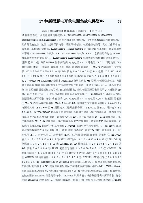
17种新型彩电开关电源集成电路资料38[ ????? | 时间:2009-03-02 01:05:33 | 收藏本文] 【大中小】17种新型彩电开关电源集成电路资料 1、KA3S0680RFB KA3S0880RFB KA3S0680RFBKA3S0880RFB是日本FAIRCHILD公司生产的开关电源电路,内置功率MOSFET和控制电路,其内部设有过流、过压、过热保护电路,低压限制电路、高压感应电路等。
具有工作频率宽、效率高、工作稳定等特点,KA3S0680RFB 与KA3S0880RFB的内部电路基本相同,只是输出功率不同(KA3S0680RFB功率为150W;KA3S0880RFB功率为190W)。
它被应用在海信DP2999、海尔高美高等新型彩电中。
KA3S0680RFB KA3S0880RFB引脚功能与维修数据见表1所示。
引脚符号功能海信DP2999 海尔高美高对地电压()对地电阻(KΩ)对地电压(V)对地电阻(KΩ)红笔测罴笔测开机待机红笔测罴笔测① DRA IN 内置功率开关管漏极300 5.7 500 270 280 3.8 ∞ ② GND 接地0 0 0 0 0 0 0 ③ Vcc 电源 20 5 500 16 15 3.3 ∞ ④ FB 反馈1.8 8 200 200 0.2 5.7 200 ⑤ SYNC 同步输入 7.1 7.5 31 6.3 3.8 5.4 30 2、A5Q1265RF A5Q1265RF是日本FAIRCHILD公司生产的FPS型开关电源控制电路,内置具有耐压强650V的电流检测型场效应功率管和控制电路,并设有过流、过压、过热保护电路(当芯片表面温度超过150℃时,自动切断输出;当供电端③脚的电压高于24V或低于11V 时,芯片停止工作)。
它被应用在海尔UOC芯片新型彩电中。
A5Q1265RF引脚功能与维修数据见表2所示引脚符号功能海尔UOC 对地电压()对地电阻(KΩ)红笔测罴笔测① DRA IN 内部场效应管漏极270 3.7 +∞ ② GND 内部场效应管源极(接地)0 0 0 ③ Vcc 电源输入端16 3.3 +∞ ④ FB 反馈输入(通常接耦合器)1 5.6 200 ⑤ SYNC 同步输入 6.3 5.3 31 3、KA7630 KA7630是具有复位信号输出功能和三路电压输出的稳压器,其内部设有限流保护电路和过热保护电路;最大输入电压20V。
- 1、下载文档前请自行甄别文档内容的完整性,平台不提供额外的编辑、内容补充、找答案等附加服务。
- 2、"仅部分预览"的文档,不可在线预览部分如存在完整性等问题,可反馈申请退款(可完整预览的文档不适用该条件!)。
- 3、如文档侵犯您的权益,请联系客服反馈,我们会尽快为您处理(人工客服工作时间:9:00-18:30)。
Symbol VIN IQ ISHDN Rds(on) ILIM1 Fsw VREF VIN,UVLO UVLO,HYS TSD VENH VENL IEN
Test Conditions VFB=0.66V EN=0
Min 1.0
Typ 100 1 150
Max 25 5
Unit V µA µA mΩ
Recommended Operating Conditions (Note 3)
Input Voltage Supply ------------------- --------------------------------------------------------------------------- 3V to 25V Junction Temperature Range ------------------------------------------------------------------------------------- -40°C to 125°C Ambient Temperature Range ------------------------------------------------------------------------------------- -40°C to 85°C
KT6008
Typical Performance Characteristics
KT6008
Output Ripple
Typical Applications
Figure 1. Schematic Diagram
Figure 2. Efficiency vs Load Current
KT6008
Pinout (top view)
(SOT23-6)
Top Mark: CAxyz (Device code: CA, x=year code, y=week code, z= lot number code Pin Name IN GND LX FB EN NC SOT23-6 5 2 1 3 4 6 Pin Description Power Input pin. Ground pin Inductor node. Connect an inductor between IN pin and LX pin. Feedback pin. Connect a resistor R1 between VOUT and FB, and a resistor R2 between FB and GND to program the output voltage: VOUT=0.6V*(R1/R2+1). Enable control. High to turn on the part. Don’t leave it floated. No connection.
Block Diagram
KT6008
KT6008
Absolute Maximum Ratings (Note 1)
LX, IN, EN ---------------------------------------------------------------------------------------------------------- 26V All other pins-------------------------- ------------------------------------------------------------------------------ 6V Power Dissipation, PD @ TA = 25°C SOT23-6 ----------------------------------------------------------------- 0.6W Package Thermal Resistance (Note 2) θ JA -------------------------------------------------------------------------------------------------------- 170°C/W θ JC -------------------------------------------------------------------------------------------------------- 130°C/W Junction Temperature Range ------------------------------------------------------------------------------------- 125°C Lead Temperature (Soldering, 10 sec.) ------------------------------------------------------------------------- 260°C Storage Temperature Range ------------------------------------------------------------------------------------- 65°C to 150°C ESD Susceptibility (Note 2) HBM (Human Body Mode) ---------------------------------------------------------------------------------------2kV MM (Machine Mode) ---------------------------------------------------------------------------------------------- 200V Dynamic LX voltage in 50ns duration --------------------------------------------------------------------- IN+3V to GND-4V
Ordering Information
KT6008 □(□□)
Applications
E:SOT-23-6 P:Green
• • • •
White LED Display Backlighting Cell Phone and Smart Phone PDA, PMP, MP3 Digital Camera
2 0.8 0.588 1 0.6
2.6 1.2 0.612 1.0 0.1 150
A MHz V V V °C V V nA
1.0 0 0.4 100
Note 1: Stresses listed as the above “Absolute Maximum Ratings” may cause permanent damage to the device. These are for stress ratings. Functional operation of the device at these or any other conditions beyond those indicated in the operational sections of the specifications is not implied. Exposure to absolute maximum rating conditions for extended periods may remain possibility to affect device reliability. Note 2: θ JA is measured in the natural convection at TA = 25°C on a low effective single layer thermal conductivity test board of JEDEC 51-3 thermal measurement standard. Test condition: Device mounted on 2” x 2” FR-4 substrate PCB, 2oz copper, with minimum recommended pad on top layer and thermal vias to bottom layer ground plane. Note 3: The device is not guaranteed to function outside its operating conditions. Note 4: IC can start up in 1.0V.
KT600Step Up Regulator Preliminary Specification
General Description
TheKT6008 SY7208 is a high efficiency, with an integrated NMOSFET current-mode and fixed frequency boost converter. The KT6008 SY7208 integrated a very low Rds-on of NMOSFTET and feedback voltage to reduce power loss and achieve high efficiency. 1MHz operate frequency and internal compensation network minimizes as few external component counts and small L and C value. SOT23-6 package provides the best solution for PCB space saving and total BOM cost.