热敏电阻阻值对照表_50K3950±1%(250度)
场效应管tk50p03参数

场效应管tk50p03参数
TK50P03是一种场效应管,通常用于功率放大和开关电路中。
它具有以下主要参数:
1. 额定电压(VDS),TK50P03的额定电压为50V,这意味着在正常工作条件下,它可以承受的最大电压为50V。
2. 额定电流(ID),TK50P03的额定电流为50A,这表示在正常工作条件下,它可以承受的最大电流为50A。
3. 阈值电压(VGS),TK50P03的阈值电压通常在2V左右,这是指在达到导通状态之前需要施加到栅极的电压。
4. 导通电阻(RDS(on)),TK50P03的导通电阻在通态时非常低,一般在几毫欧姆到几十毫欧姆之间,这意味着它在导通状态时可以提供较低的电阻。
5. 封装类型,TK50P03通常采用TO-220或者TO-263等标准封装。
总的来说,TK50P03是一款功率较大的场效应管,适用于需要承受较高电压和电流的电路中。
在设计电路时,需要根据其参数来合理选择工作条件和外围元器件,以确保电路稳定可靠地工作。
RT9705B 1 DS9705B-03 电源多路复用器说明书
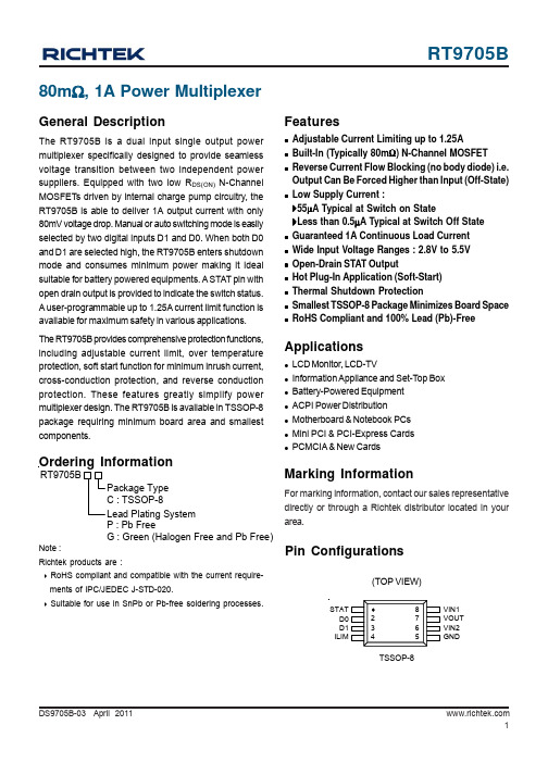
DS9705B-03 April 201180m Ω, 1A Power MultiplexerGeneral DescriptionThe RT9705B is a dual input single output power multiplexer specifically designed to provide seamless voltage transition between two independent power suppliers. Equipped with two low R DS(ON) N-Channel MOSFETs driven by internal charge pump circuitry, the RT9705B is able to deliver 1A output current with only 80mV voltage drop. Manual or auto switching mode is easily selected by two digital inputs D1 and D0. When both D0and D1 are selected high, the RT9705B enters shutdown mode and consumes minimum power making it ideal suitable for battery powered equipments. A STAT pin with open drain output is provided to indicate the switch status.A user-programmable up to 1.25A current limit function is available for maximum safety in various applications.The RT9705B provides comprehensive protection functions,including adjustable current limit, over temperature protection, soft start function for minimum inrush current,cross-conduction protection, and reverse conduction protection. These features greatly simplify power multiplexer design. The RT9705B is available in TSSOP-8package requiring minimum board area and smallest components.Featuresz Adjustable Current Limiting up to 1.25Az Built-In (Typically 80m Ω) N-Channel MOSFET zReverse Current Flow Blocking (no body diode) i.e.Output Can Be Forced Higher than Input (Off-State)zLow Supply Current :`55μA Typical at Switch on State`Less than 0.5μA Typical at Switch Off State z Guaranteed 1A Continuous Load Current z Wide Input Voltage Ranges : 2.8V to 5.5V z Open-Drain STAT Outputz Hot Plug-In Application (Soft-Start)z Thermal Shutdown Protectionz Smallest TSSOP-8 Package Minimizes Board Space zRoHS Compliant and 100% Lead (Pb)-FreeApplicationsz LCD Monitor, LCD-TVz Information Appliance and Set-Top Box z Battery-Powered Equipment z ACPI Power Distributionz Motherboard & Notebook PCs z Mini PCI & PCI-Express Cards zPCMCIA & New CardsPin Configurations(TOP VIEW)TSSOP-8Ordering InformationSTAT D0D1ILIMGNDVIN2VOUT VIN1Note :Richtek products are :` RoHS compliant and compatible with the current require-ments of IPC/JEDEC J-STD-020.` Suitable for use in SnPb or Pb-free soldering processes.Marking InformationFor marking information, contact our sales representative directly or through a Richtek distributor located in yourarea.Package Type C : TSSOP-8RT9705BLead Plating System P : Pb FreeG : Green (Halogen Free and Pb Free)Typical Application CircuitTable 1. Truth TableNotes for Table 1.1. X : Don ’t care2. Hi-Z: High impedance node3. D0 and D1 cannot be floating which will lead to an unknown state.4. An internal MOSFET with 2k Ω R DS(ON) turns on and softly discharges the output voltage when D0 = D1 = 1.V V OUTDS9705B-03 April 2011Test CircuitsTest Circuit 1Test Circuit 2Test Circuit 3Test Circuit 4f = 28Hzf = 580Hz5VV OUTFunction Block DiagramTiming DiagramV 5VQ1 EnabledQ2 EnabledV 3.3VV OUT (a)(b)(c)DS9705B-03 April 2011Electrical Characteristicsz Input Voltage, VIN1 & VIN2-----------------------------------------------------------------------------------------−0.3V to 6.0V z Logic Inputs Voltage, D0 &D1--------------------------------------------------------------------------------------−0.3V to 6.0V z Output Voltage, VOUT , STAT & ILIM -----------------------------------------------------------------------------−0.3V to 6.0V zPower Dissipation, P D @ T A = 25°CTSSOP-8----------------------------------------------------------------------------------------------------------------0.43W zPackage Thermal Resistance (Note 2)TSSOP-8, θJA ----------------------------------------------------------------------------------------------------------230°C/W z Junction T emperature -------------------------------------------------------------------------------------------------125°C z Lead Temperature (Soldering, 10 sec.)---------------------------------------------------------------------------260°Cz Storage T emperature Range ----------------------------------------------------------------------------------------−65°C to 150°C zESD Susceptibility (Note 3)HBM (Human Body Mode)------------------------------------------------------------------------------------------2kV MM (Machine Mode)--------------------------------------------------------------------------------------------------200VAbsolute Maximum Ratings (Note 1)To be continuedRecommended Operating Conditions (Note 4)zInput VoltageV IN1 ( if V IN2 2.8V)--------------------------------------------------------------------------------------------------2.3V to 5.5V V IN1 ( if V IN2 < 2.8V)--------------------------------------------------------------------------------------------------2.8V to 5.5V V IN2 ( if V IN1 2.8V)--------------------------------------------------------------------------------------------------2.3V to 5.5V V IN2 ( if V IN1 < 2.8V)--------------------------------------------------------------------------------------------------2.8V to 5.5V z Logic Inputs Voltage (D0 &D1)-------------------------------------------------------------------------------------0V to 5.5V z Junction T emperature Range ----------------------------------------------------------------------------------------−40°C to 125°C z Ambient T emperature Range ----------------------------------------------------------------------------------------−40°C to 85°C≥≥To be continuedDS9705B-03 April 2011Note 1. Stresses listed as the above “Absolute MaximumRatings ” may cause permanent damage to the device. These are for stress ratings. Functional operation of the device at these or any other conditions beyond those indicated in the operational sections of the specifications is not implied.Exposure to absolute maximum rating conditions for extended periods may remain possibility to affect device reliability.Note 2. θJA is measured in the natural convection atT A = 25°C on a low effective thermal conductivity test board of JEDEC 51-3 thermal measurement standard.Note 3. Devices are ESD sensitive. Handling precautionrecommended.Note 4. The device is not guaranteed to function outside itsoperating conditions.Note 5. Performance at −5°C ≤ T A ≤ 85°C is assured bydesign.Note 6. Not tested for production.Note 7. The UVLO is without latch. In V IN falling dege, theoutput voltage will depend on I OUT and C OUT . Please see below curve as reference.V IN2 = 2.2V, C OUT = 10uF, R L = 180ΩV OUT Response vs. UVLOTime (1ms/Div)V OUT(1V/Div)V IN1(1V/Div)R DS(ON) vs. Temperature5060708090100110-50-25255075100125Temperature (°C)R D S (O N ) (m Ω)Typical Operating CharacteristicsR e f e r t o T e s t C i r c u i t s 2Output Turn-On ResponseTime (1ms/Div)D0D1V OUT(2V/Div)(2V/Div)(2V/Div)D0 = 1 0, D1 = 1, V IN1 = 5V, V IN2 = 3.3V↔Output Switchover ResponseTime (1ms/Div)D1D0V OUT(2V/Div)(2V/Div)(2V/Div)D0 = 0, D1 = 1 0V IN1 = 5V, V IN2 = 3.3V↔R e f e r t o T e s t C i r c u i t s 1Current Limit vs. Junction Temperature00.20.40.60.811.21.41.61.82-50-25255075100125Junction Temperature C u rr e n t L i m i t (A )(°C)R DS(ON) vs. Input Voltage606570758085902.53 3.54 4.55 5.56Input Voltage (V)R D S (O N ) (m Ω)Quiescent Current vs. Input Voltage303540455055602.53 3.54 4.55 5.56Input Voltage (V)Q u i e s c e n t C u r r en t (u A )DS9705B-03 April 2011Output Switchover Voltage DroopTime (50μs/Div)D1V OUT(2V/Div)(2V/Div), C OUT = 1uF (2V/Div), C OUT = openD0 = 0, D1 = 1 0, V IN1 = V IN2 = 5V, RL = 50Ω↔R e f e r t o T e s t C i r c u i t s 3Auto Switchover Voltage DroopTime (250μs/Div)(2V/Div)(2V/Div)V OUTV IN1D0 = 1, D1 = 0, V IN1 = 5 0V, V IN2 = 3.3V↔R e f e r t o T e s t C i r c u i t s 4Output Switchover Voltage Droop vs. C OUT00.20.40.60.811.21.41.60.1110100C OUT (uF)O u t p u t S w i t c h o v e r V o l t a g e D r o o p (V )Application InformationThe RT9705B is dual input single output power multiplexer specifically designed to provide seamless voltage transition between two independent power suppliers. Equipped with two low R DS(ON) N-Channel MOSFETs driven by internal charge pump circuitry, the RT9705B is able to deliver 1A output current with only 80mV voltage drop. The RT9705B provides comprehensive protection functions, including adjustable current limit, over temperature protection, soft start function for minimum inrush current, cross-conduction protection, and reverse conduction protection. These features greatly simplify power multiplexer design.Manual Switching ModeThe RT9705B provides two logic input D0 and D1 for switch selection as shown in Table 1. The RT9705B selects the manual-switching mode when the D0 is pulled low. In this mode V OUT connects to V IN1 if D1 pulled high, otherwise V OUT connects to V IN2.Auto Switching ModeRT9705B selects the auto-switching mode when the D0 is pulled high and D1 is pulled low. In this mode V OUT connects to the higher of V IN1 and V IN2.Shutdown ModeWhen both D0 and D1 are selected high, the RT9705B enters shutdown mode and consumes minimum power. An internal MOSFET with 2kΩ R DS(ON) turns on and softly discharges the output voltage in the shutdown mode. Since no body diode exists between V INX and V OUT, output voltage is allowed to be high than the input voltages in the shutdown mode.Switch Status IndicationA STAT pin with open drain output is provided to indicate the switch status. STAT pin outputs high impedance if V IN2 is active, otherwise STAT pin outputs low.Current LimitingThe current limit circuitry prevents damage to the MOSFET switch and external load. A resistor R ILIM from ILIM to GND sets the current limit to 500/R ILIM and the adjustable current limiting up to 1.25 A. A setting resistor R ILIM equal to zero is not recommended as that disables current limiting.Thermal ConsiderationsThermal protection limits power dissipation in RT9705B. When the operation junction temperature exceeds 135°C, the OTP circuit starts the thermal shutdown function and turns the pass element off. The pass element turn on again after the junction temperature cools by 10°C.For continuous operation, do not exceed absolute maximum operation junction temperature 125°C. The power dissipation definition in device is :P D = (V IN-V OUT) x I OUT + V IN x I QThe maximum power dissipation depends on the thermal resistance of IC package, PCB layout, the rate of surroundings airflow and temperature difference between junction to ambient. The maximum power dissipation can be calculated by following formula :P D(MAX) = ( T J(MAX) - T A ) / θJAwhere T J(MAX) is the maximum operation junction temperature 125°C, T A is the ambient temperature and the θJA is the junction to ambient thermal resistance.For recommended operating conditions specification of RT9705B, where T J(MAX) is the maximum junction temperature of the die (125°C) and T A is the maximum ambient temperature. The junction to ambient thermal resistance (θJA is layout dependent) for TSSOP-8 package is 230°C/W on standard JEDEC 51-3 thermal test board. The maximum power dissipation at T A = 25°C can be calculated by following formula :P D(MAX) = (125°C -25°C) / 230°C/W = 430 mW (TSSOP-8)RT9705B11DS9705B-03 April 2011Layout ConsiderationIn order to meet the voltage drop, droop, and EMI requirements, careful PCB layout is necessary. The following guidelines must be considered :zKeep all main current traces as short and wide as possible.z Place a ground plane under all circuitry to lower both resistance and inductance and improve DC and transient performance (Use a separate ground and power plans if possible).zLocate the ceramic input capacitors as close as possible to the VIN and GND pins of the device.Figure 1. Top Layer Figure 2. Bottom Layer12DS9705B-03 April Richtek Technology CorporationHeadquarter5F, No. 20, Taiyuen Street, Chupei CityHsinchu, Taiwan, R.O.C.Tel: (8863)5526789 Fax: (8863)5526611Richtek Technology Corporation Taipei Office (Marketing)5F, No. 95, Minchiuan Road, Hsintien City Taipei County, Taiwan, R.O.C.Tel: (8862)86672399 Fax: (8862)86672377Email:*********************Information that is provided by Richtek Technology Corporation is believed to be accurate and reliable. Richtek reserves the right to make any change in circuit design,specification or other related things if necessary without notice at any time. No third party intellectual property infringement of the applications should be guaranteed by users when integrating Richtek products into any application. No legal responsibility for any said applications is assumed by Richtek.8-Lead TSSOP Plastic Package。
苏州百合科技有限责任公司 ZL-7901A 智能温湿度控制器 安装使用说明书

ZL-7901A 智能温湿度控制器安装使用说明书 软件版本 V2.6产品简介ZL-7901A 是一款工业级智能温湿度控制器,可外接SSR 扩展输出,并采用PID 控制方式实现高精度温度控制。
它采用触摸按键及LCD 大屏显示设计,操作简捷安装方便,适用于禽蛋孵化器、人工气候室、仓储等场合的温湿度控制。
主要功能说明1.对温度控制,有三种控制方式。
可选择PID 方式实现高精度温控2.加湿或除湿控制3.定时换气控制4.定时翻蛋控制5.照明控制6.节点型报警输出7.断电记忆功能8.温度/湿度超限报警及保护功能 9.温度/湿度传感器故障报警及保护功能主要技术指标◇电源电压: 100~240VAC,50~60Hz ◇控制资源:继电器输出(8路) 模拟量输入(2路) 主温控继电器 250VAC 7.5A 阻性负载 R1 NTC 温度传感器5K/3470 辅助温控继电器 7.5A R2 湿度传感器SHR04 湿度控制继电器 7.5AR3照明灯继电器 7.5AR4换气继电器 3A R5翻蛋控制继电器 1A R6/R7 报警输出继电器 1AR8/R9 SSR 固态继电器20mA/10VDC MAXY+/Y-◇设定范围:湿度0~99% RH;温度0~100℃ ◇测量精度:温度1%@25℃;湿度3%@25℃ ◇工作环境:-20~45℃;10~90% RH 无结露产品版本上电,显示产品型号(7901A )和版本号(2.6):按键与显示说明按键定义功能说明电源长按3秒,开机或关机设置短按此键,进行温湿度设置;长按此键,进行参数设置设置+ 累加键,长按此键设置参数快速增加设置- 累减键,长按此键设置参数快速递减确认设置参数时,按此键确认设置参数复位短按此键,参数设置返回键;长按3秒,孵化天数累计清除照明开关按此键,开/关照明灯功能组合按键操作显示说明图标功能亮灭闪烁加湿/除湿状态运行停机主加热器运行停机辅助加热器运行停机换气运行停机翻蛋电机右转运行停机翻蛋电机左转运行停机报警--- 无报警报警E01 温度传感器故障报警无报警E02 湿度传感器故障报警无报警tHi 温度超上限报警无报警tLo 温度超下限报警无报警HHi 湿度超上限报警无报警HLo 湿度超下限报警无报警UnL 恢复默认参数恢复默认参数提示音每次按键,有提示音。
插卡取电开关行业,核心元器件,50A大功率继电器
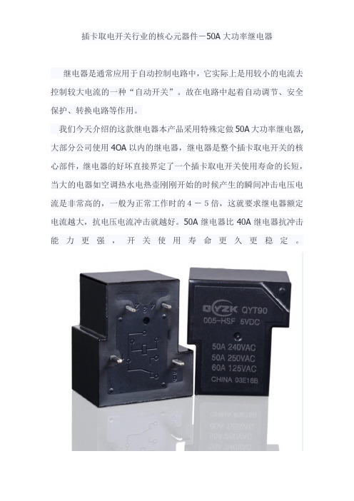
插卡取电开关行业的核心元器件-50A大功率继电器
继电器是通常应用于自动控制电路中,它实际上是用较小的电流去控制较大电流的一种“自动开关”。
故在电路中起着自动调节、安全保护、转换电路等作用。
我们今天介绍的这款继电器本产品采用特殊定做50A大功率继电器,大部分公司使用4OA以内的继电器,继电器是整个插卡取电开关的核心部件,继电器的好坏直接界定了一个插卡取电开关使用寿命的长短,当大的电器如空调热水电热壶刚刚开始的时候产生的瞬间冲击电压电流是非常高的,一般为正常工作时的4-5倍,这就要求继电器额定电流越大,抗电压电流冲击就越好。
50A继电器比40A继电器抗冲击能力更强,开关使用寿命更久更稳定。
所以说,群鹰智控的这款50A大功率继电器,可以为您保驾护航,插卡取电开关行业指定供应商!。
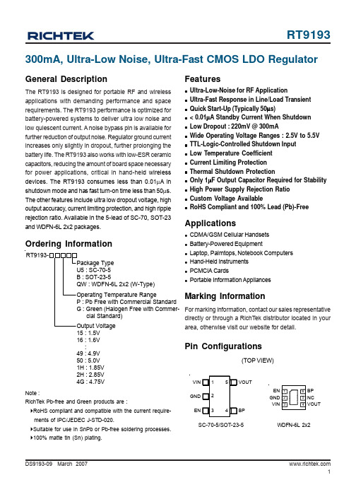
RT9193-50GU5资料
Recommended Operating Conditions
z z z z
Supply Input Voltage -----------------------------------------------------------------------------------------------------EN Input Voltage ----------------------------------------------------------------------------------------------------------Junction Temperature Range -------------------------------------------------------------------------------------------Ambient Temperature Range --------------------------------------------------------------------------------------------
Note : RichTek Pb-free and Green products are : `RoHS compliant and compatible with the current requirements of IPC/JEDEC J-STD-020. `Suitable for use in SnPb or Pb-free soldering processes. `100% matte tin (Sn) plating.
Features
z z z z z z z z z z z z z z
UC3550L-50-AF5-R资料
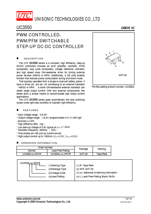
UNISONIC TECHNOLOGIES CO., LTDUC3550 CMOS ICPWM CONTROLLED , PWM/PFM SWITCHABLESTEP-UP DC-DC CONTROLLERDESCRIPTIONThe UTC UC3550 series is a compact, high efficiency, step-up DC/DC controllers includes an error amplifier, oscillator, PWM comparator, skip cycle comparator, voltage reference, soft-start, and high speed lower ON-resistance driver for driving external power devices (NMOS or NPN) ,Additionally, a CE (chip enable) function that reduces power consumption during shut-down mode. That typically operated from a single-or dual-cell battery packs. It have a driver pin ,ext pin, for connecting to an external transistor(NMOS or NPN . a lower ON-resistance external transistor can obtain larger output current. With only external components, this series allow a simple means to accommodate high output current applications.The UTC UC3550 series goes automatically into skip switching cycles under light load condition to maintain high efficiency.FEATURES* Input voltage range :0.9~8V* Output voltage range :1.8~6V programmable in 0.1V with high accuracy ± 2.5%* High efficiency 88%(typ.)* Low start-up voltage of 0.9V typical at I OUT = 1.0mA * Oscillator frequency: 300kHz.( 20%) * Chip enable pin with pull-up current source* High output current up to 1000mA (V IN = 2.0V, V OUT =3.3V)*Pb-free plating product number: UC3550LORDERING INFORMATIONOrder NumberNormal Lead Free PlatingPackage PackingUC3550-xx-AF5-R UC3550L-xx-AF5-R SOT-25 Tape ReelMARKING INFORMATIONPIN CONFIGURATIONOUT EXTCE GNDNCPIN DESCRIPTIONPIN NOPIN NAMEDESCRIPTION1 CE Chip Enable:The chip is enabled if a voltage equal to or greater than 1.0V or left floating is applied.The chip is disabled if a voltage less than 0.3V is applied.2 OUT Output voltage monitor, IC internal power supply3 NC No connection4 GND Ground5 EXT External transistor driveBLOCK DIAGRAM5 EXTCE 1ABSOLUTE MAXIMUM RATINGPARAMETER SYMBOL RATINGS UNITSupply Voltage V OUT -0.3~8 VEXT VoltageV EXT -0.3 ~ 8 V EXT Sink/Source Current I EXT -150 ~ +150 mACE Input Voltage Range V CE -0.3 ~ 12.0 VCE Input Current Range I CE -155 ~ 155 mA Power Dissipation (Ta=25 ) P D 500 mW Junction Temperature T J +150 Operating Temperature T OPR -40 ~ +85 Storage Temperature T STG -55 ~ +150 Note: Absolute maximum ratings are those values beyond which the device could be permanently damaged.Absolute maximum ratings are stress ratings only and functional device operation is not implied. THERMAL DATAPARAMETER SYMBOL RATINGS UNITThermal Resistance Junction to Air θJA 250 /WELECTRICAL CHARACTERISTICS (Ta=25 , f OSC =300kHz, unless otherwise specified)UC3550-3.3VPARAMETER SYMBOL TEST CONDITIONS MIN TYP MAX UNITOSCILLATOR Frequency f OSC V OUT =V SET ×0.96 240 300 360 kHz Frequency Temperature Coefficient f Ta =-40 ~ 85 0.10 %/ Maximum PWM Duty Cycle D MAX V OUT =V SET ×0.96 70 80 90 % Minimum Start-up Voltage V START1 I OUT =0mA 800 900 mV Minimum Start-up Voltage V START2 I OUT =1mA 900 1000 mV Minimum Start-up Voltage Temperature CoefficientV START Ta=-40 ~ 85 -1.6mV/Minimum Operation Hold Voltage V OPR I OUT =0mA 600 700 mV Soft-Start Time t SS V OUT =V SET 60 250 ms CE (PIN 1)V CEH 900 mV CE Input Voltage : High State, Device Enabled Low State, Device Disabled V CELV OUT =V SET ×0.96680 mVI CEHV OUT =V CE =5.0V -0.5 0 0.5 µACE Input Current : High State, Device Enabled Low State, Device Disabled I CEL V OUT =5.0V, V CE =0V 0 0.15 0.5 µA EXT (PIN 5) EXT “H”R EXTH V EXT =V OUT -0.4V 11 15 Ω ON ResistanceEXT “L”R EXTLV EXT =0.4V 8 12 ΩTOTAL DEVICEOutput Voltage V OUT3.2183.3 3.383 VOutput Voltagetemperature coefficient V OUT Ta=-40 ~ 85150ppm/Operating Current I DD V OUT =V CE =V SET ×0.96 103 160 µA Stand-by Current I STN-BY V OUT =V CE =V SET +0.5V 15 38 µAOff-State Current I OFF V OUT =5.0V, V CE =0V,Ta=-40 ~ +850.6 1.5 µAEfficiency ηI OUT = 200mA, V IN = 2.0V 80 88 %ELECTRICAL CHARACTERISTICS (Cont.)UC3550-5.0VPARAMETER SYMBOL TEST CONDITIONS MIN TYP MAX UNITOSCILLATOR Frequency f OSC V OUT =V SET ×0.96 240 300 360 kHz Frequency Temperature Coefficient f Ta =-40 ~ 85 0.1 %/ Maximum PWM Duty Cycle D MAX V OUT =V SET ×0.96 70 80 90 % Minimum Start-up Voltage V START1I OUT =0mA 800 900 mV Minimum Start-up Voltage V START2I OUT =1mA 900 1 V Minimum Start-up Voltage Temperature CoefficientV START Ta=-40 ~ 85 -1.6mV/Minimum Operation Hold Voltage V OPR I OUT =0mA 600 700 mV Soft-Start Time t SS V OUT =V SET 60 200 ms CE (PIN 1)V CEH 900 mV CE Input Voltage :High State, Device Enabled Low State, Device Disabled V CEL V OUT =V SET ×0.96 680 mV I CEH V OUT =V CE = 5.0V -0.5 0 0.5 µA CE Input Current :High State, Device Enabled Low State, Device DisabledI CEL V OUT =5.0V, V CE =0V 0 0.15 0.5 µAEXT (PIN 5) EXT “H” R EXTH V EXT =V OUT -0.4V 6 10 ΩON ResistanceEXT “L” R EXTL V EXT =0.4V 6 10 Ω TOTAL DEVICEOutput Voltage V OUT 4.875 5 5.125 V Output Voltage temperature coefficient V OUT Ta=-40 ~ 85 150ppm/Operating Current I DD V OUT =V CE =V SET ×0.96 136 220 µA Stand-by Current I STN-BY V OUT =V CE =V SET +0.5V 15 38 µAOff-State Current I OFFV OUT =5.0V, V CE =0V,Ta=-40 ~ +850.6 1.5 µA Efficiency η I OUT = 200mA, V IN = 2.0V 80 88 %TYPICAL STEP-UP CONVERTER APPLICATIONOUT V INStep -up Converter using external MOSFETV OUT V uFStep -up Converter using external NPNRecommended componentsNmosTr :XP161A0390PR/ (Torex) or NTGS3446T1(ON SEMI ) L :10Uh(sunida CD54 fosc =300kHz) SD :MA737, or MBRM110L Cin :10V 10uF (tantalum)CL :16V220uF(tantalum)NPN Tr typeTr :2SD1628(Sanyo),MMJT9410Rb :500~1000Ω(Adjust according to load and Tr. h FE levels) Cb :3000p (ceramic type )EXTERNAL COMPONENT SELECTIONInductor SelectionAn inductor value of 10uH performs well in most application. The UC3550 series also work with inductors in the 4.7uH to 12uH range. An inductor with higher peak inductor current tends a higher output voltage ripple(I PEAK x output filter capacitor ESR). The inductor’s DC resistance significantly affects efficiency.Output Capacitor SelectionThe output ripple voltage(I PEAK x output filter capacitor ESR)is the product of the peak inductor current and the output capacitor Equivalent Series Resistance (ESR). Best performances are obtained with good high frequency characteristics capacitors and low ESR. The best compromise for the value of the Output Capacitance is 220F Tantalum Capacitor. The output capacitor as close as possible to the device pins.Input Capacitor SelectionThe Input Capacitor is required to compensate, if present, the series impedance between the Supply Voltagefor distances less Source and the Input Voltage of the Application. A value of 10 F is enough to guarantee stabilitythan 2". In any case we suggest to connect both capacitors, The input capacitor as close as possible to the device pins.Diode SelectionThe Schottky diode with an high switching speed and a very low Forward Voltage (VF) is needed. Higher VF may cause lost power as heat in the diode, with a decrease of the Efficiency. Moreover, since the Output Voltage pin is also used as the device Supply Voltage, the Start-up Voltage (see related plots) is strictly due to the diode Forward Voltage at the rated Forward Current.External Component SelectionAn enhancement N-channel MOSFET or a bipolar NPN transistor can be used as the external switch transistor. since enhancement N-channel MOSFET is a voltage driven device, it is a more efficient switch than a BJT transistor. However, he MOSFET requires a higher voltage to turn on as compared with BJT transistorFor enhancement N-channel MOSFET ( it is especially importance for R DS(ON),typically<0.1Ω, threshold voltage, V GS(TH) must be<V OUT, typically<1.5V.For bipolar NPN transistor, continuous collector current typically 1A to 4A and V CE(SAT)<0.2V. the driving capability is determined by the DC current gain, H FE, of the transistor and the base resistor, Rb. Moreover, a speed-up capacitor, Cb should be connected in paralled with Rb to reduce switch loss and improve efficiency.TYPICAL CHARACTERISTICSN O L o a d I n p u t C u r r e n t , I I N (m A )No Load InputCurrent vs. Input Voltage (Using MOSFET) Input Voltage , V IN (V)N O L o a d I n p u t C u r r e n t , I I N (m A )Input Voltage, V IN (V)No Load InputCurrent vs. Input Voltage (Using BJT)1000004.84.95.02004.740060080010005.15.2O F F -S t a t e C u r r e n t , I O F F (µA )V OUT (V)Off-State Current vs. V OUTO u tp u t V o l t a g e , V O U T (V )Output Current, I OUT (mA)Output Voltage vs. Output Current3.060708009010050Output Voltage vs. Output Current3.13.23.33.43.5Output Current, I O (mA)O u t p u t V o l t a g e , V O U T (V )Maximum Duty Cycle vs. TemperatureTemperature (℃)M a x i m u m D u t y C y c l e , D M A X (%)TYPICAL CHARACTERISTICS(Cont.)0.010.11101001000Efficiency vs Output Current(5.0V) 00.40.81.2204060801001.620E f f i c i e n c y (%)Output Current, I OUT (mA)Startup/Hold Voltage vs Output Current (Using MOSFET)Output Current (3.3V) Output Current, I C (mA)S t a r t u p /H o l d V o l t a g e , V s t a r t /V h o ld (V )-5051015-2502550100202575002004006008001000600EXT ON-Resistance vs TemperatureO N -R e s i s t a n c e , (Ω)Temperature ℃Output Current, I OUT (mA)R i p p l e V o l t a g e , V R I P P L E (m V )-50-25255010075-50-250255010075 Oscillator Frequency vs. TemperatureTemperature (℃)O s c i l a t o r F r e q u e n c y , f o s c (K H z )Oscillator Frequency vs. Temperature O s c i l a t o r F r e q u e n c y , f o s c (K H z )TYPICAL CHARACTERISTICS(Cont.)。
AH3503 霍尔开关
0.85 8
9
10
11
12
电源电压 (V) CS3501 归一化灵敏度与电源电压关系曲线
1.05
1.00
Vcc=12V
0.95
B=100mT
RL=10KΩ
0.90
0
25
50
75
环境温度(℃) CS3501 归一化灵敏度与环境温度关系曲线
5.00
4.00 3.00
TA=25℃ B=0mT
2.00
4.06±0.10
0.8 1.5+00.1
2.03
0.43
0.38
0.38
1.27 2.54
45o
1 23
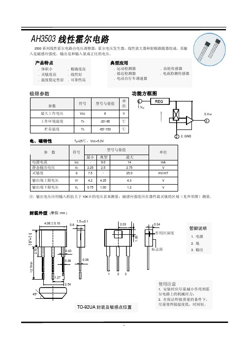
TO-92UA 封装及敏感点位置
0.34 作用区深度
标志面
管脚说明
1. 电源 2. 地 3. 输出
使用注意
1. 安装时应尽量减小作用到霍 尔电路上的机械应力; 2. 在保证焊接质量的条件下, 尽量使焊接温度低,时间短。
符号
Icc Vo S VT VL
最小 -
2.25 7.5
4.2
0.75
型号与量值
典型 9.0 2.5
-
最大 14 2.75
25.0
4.25
4.3
1.00
1.2
Hale Waihona Puke 单位mA V mV/mT V V
注: 输出电压应用输入阻抗大于 10KΩ的电压表来测量;磁感应强度应在器件最灵敏的区域(见外形图)测量。
封装外型 (单位: mm )
AH3503 线性霍尔电路
3500 系列线性霍尔电路由电压调整器,霍尔电压发生器,线性放大器和射极跟随器组成,其输 入是磁感应强度,输出是和输入量成正比的电压。
851a芯片参数
851a芯片是一种高性能的音频功率放大器芯片,常用于音频放大器和音响系统中。
以下是该芯片的主要参数:
供电电压:±12V ~ ±40V
输出功率:100W(THD+N=10%,RL=8Ω,f=1kHz)
工作温度范围:-40℃~ +85℃
输入阻抗:47kΩ
噪声电平:≤100μV
失真率:≤0.1%
频率响应范围:20Hz ~ 20kHz
封装形式:TO-220-15
851a芯片采用了多种保护电路,包括过热保护、过流保护、过压保护和欠压保护等,可以有效地保护芯片和外部设备。
该芯片还支持单电源和双电源供电,适用于不同的应用场景。
需要注意的是,851a芯片是一种高功率放大器芯片,使用时需要注意安全和稳定性。
在设计和使用电路时,应该遵循相关的规范和最佳实践,以确保设备的可靠性和安全性。