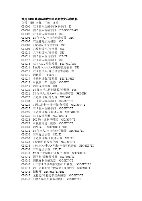
CD4023 CMOS 三3输入与非门
cmos或非门电路

cmos或非门电路CMOS或非门电路CMOS(Complementary Metal-Oxide-Semiconductor)是一种常用的集成电路技术,它在现代电子设备中得到广泛应用。
而非门电路是CMOS技术中的一种基本电路,用于实现逻辑运算。
本文将重点介绍CMOS和非门电路的原理、应用以及优势。
一、CMOS技术的原理CMOS技术是利用PN结的正负偏压控制MOS管的导通和截止,从而实现电路的功能。
CMOS电路由PMOS和NMOS管组成,PMOS管的特点是在负偏压下导通,而NMOS管则在正偏压下导通。
通过控制这两种管的导通和截止,可以实现逻辑运算。
二、非门电路的构成和工作原理非门电路是CMOS技术中的一种基本逻辑门电路,用于实现逻辑非运算。
非门电路由两个MOS管组成,一个是PMOS管,另一个是NMOS管。
当输入信号为低电平时,PMOS管导通,NMOS管截止,输出信号为高电平;当输入信号为高电平时,PMOS管截止,NMOS管导通,输出信号为低电平。
通过这种方式,非门电路可以实现逻辑非运算。
三、非门电路的应用非门电路在数字电路和计算机系统中有着广泛的应用。
它可以用于构建各种逻辑电路,例如与门、或门、异或门等。
非门电路还可以用于实现数字信号的转换和处理,例如将正逻辑信号转换为负逻辑信号,或者将负逻辑信号转换为正逻辑信号。
四、CMOS技术的优势CMOS技术相比于其他集成电路技术具有以下优势:1. 低功耗:CMOS电路的功耗非常低,因为只有在切换时才会消耗能量,而在静态状态下基本不消耗能量。
2. 高集成度:CMOS技术可以实现高度集成的电路,因为它的元件尺寸小,布局紧凑,可以在一块芯片上集成大量的电路。
3. 抗干扰能力强:CMOS电路的输入和输出都是电压信号,不容易受到外界的干扰,因此具有很好的抗干扰能力。
4. 工艺成熟:CMOS技术是一种成熟的制造工艺,已经得到广泛应用。
它的制造过程简单,可靠性高。
五、结论CMOS技术和非门电路是现代电子设备中不可或缺的组成部分。
cmos或非门电路

cmos或非门电路CMOS (Complementary Metal-Oxide-Semiconductor) 和非门电路是数字电路中常见的基本逻辑门电路。
这两种电路在现代电子技术中扮演着重要的角色。
下面将为您介绍这两种电路的历史、原理和应用。
CMOS电路最早出现在20世纪60年代,当时是由Fairchild公司的工程师研制出来的。
CMOS电路最大的特点就是功耗低、可靠性高,因此在现代集成电路中得到广泛应用。
CMOS电路的原理是利用p型金属-氧化物-半导体(pMOS)晶体管和n型金属-氧化物-半导体(nMOS)晶体管的互补特性,实现高阻抗输入、低阻抗输出的逻辑运算。
CMOS电路具有许多优点,例如低功耗、高可靠性和良好的抗干扰性。
由于这些优点,CMOS电路被广泛应用于数字电路、模拟电路和微处理器中。
此外,CMOS电路在单片集成电路中的应用也日益广泛。
非门电路是由两个逻辑门(或称为反相器)组成的电路,其中一个门输出与输入信号相反,另一个门输出与输入信号相同。
非门电路的原理是利用反相器实现逻辑运算。
非门电路是最基本的数字逻辑电路之一。
非门电路的应用很广泛。
例如,在计算机内存中,非门电路被用来检测并修复存储单元的错误。
在数字电路中,非门电路被用来实现布尔函数的取反操作。
此外,非门电路还被用来实现流水线寄存器中的时钟控制信号。
总之,CMOS电路和非门电路都是数字电路中非常常见和重要的电路。
它们提供了许多重要的功能,被广泛应用于计算机和其他数字电路中。
随着电子技术的不断发展,这两种电路的应用将继续扩大。
CD系列引脚大全
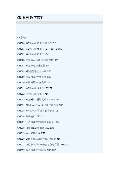
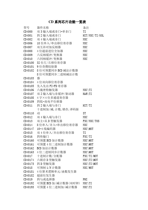
常用4000系列标准数字电路的中文名称资料型号器件名称厂牌备注CD4000 双3输入端或非门+单非门 TICD4001 四2输入端或非门 HIT/NSC/TI/GOLCD4002 双4输入端或非门 NSCCD4006 18位串入/串出移位寄存器 NSCCD4007 双互补对加反相器 NSCCD4008 4位超前进位全加器 NSCCD4009 六反相缓冲/变换器 NSCCD4010 六同相缓冲/变换器 NSCCD4011 四2输入端与非门 HIT/TICD4012 双4输入端与非门 NSCCD4013 双主-从D型触发器 FSC/NSC/TOSCD4014 8位串入/并入-串出移位寄存器 NSCCD4015 双4位串入/并出移位寄存器 TICD4016 四传输门 FSC/TICD4017 十进制计数/分配器 FSC/TI/MOTCD4018 可预制1/N计数器 NSC/MOTCD4019 四与或选择器 PHICD4020 14级串行二进制计数/分频器 FSCCD4021 08位串入/并入-串出移位寄存器 PHI/NSCCD4022 八进制计数/分配器 NSC/MOTCD4023 三3输入端与非门 NSC/MOT/TICD4024 7级二进制串行计数/分频器 NSC/MOT/TICD4025 三3输入端或非门 NSC/MOT/TICD4026 十进制计数/7段译码器 NSC/MOT/TICD4027 双J-K触发器 NSC/MOT/TICD4028 BCD码十进制译码器 NSC/MOT/TICD4029 可预置可逆计数器 NSC/MOT/TICD4030 四异或门 NSC/MOT/TI/GOLCD4031 64位串入/串出移位存储器 NSC/MOT/TICD4032 三串行加法器 NSC/TICD4033 十进制计数/7段译码器 NSC/TICD4034 8位通用总线寄存器 NSC/MOT/TICD4035 4位并入/串入-并出/串出移位寄存 NSC/MOT/TI CD4038 三串行加法器 NSC/TICD4040 12级二进制串行计数/分频器 NSC/MOT/TICD4041 四同相/反相缓冲器 NSC/MOT/TICD4042 四锁存D型触发器 NSC/MOT/TICD4043 4三态R-S锁存触发器("1"触发) NSC/MOT/TI CD4044 四三态R-S锁存触发器("0"触发) NSC/MOT/TI CD4046 锁相环 NSC/MOT/TI/PHICD4047 无稳态/单稳态多谐振荡器 NSC/MOT/TICD4048 4输入端可扩展多功能门 NSC/HIT/TICD4049 六反相缓冲/变换器 NSC/HIT/TICD4050 六同相缓冲/变换器 NSC/MOT/TICD4051 八选一模拟开关 NSC/MOT/TICD4052 双4选1模拟开关 NSC/MOT/TICD4053 三组二路模拟开关 NSC/MOT/TICD4054 液晶显示驱动器 NSC/HIT/TICD4055 BCD-7段译码/液晶驱动器 NSC/HIT/TI CD4056 液晶显示驱动器 NSC/HIT/TICD4059 “N”分频计数器 NSC/TICD4060 14级二进制串行计数/分频器 NSC/TI/MOT CD4063 四位数字比较器 NSC/HIT/TICD4066 四传输门 NSC/TI/MOTCD4067 16选1模拟开关 NSC/TICD4068 八输入端与非门/与门 NSC/HIT/TICD4069 六反相器 NSC/HIT/TICD4070 四异或门 NSC/HIT/TICD4071 四2输入端或门 NSC/TICD4072 双4输入端或门 NSC/TICD4073 三3输入端与门 NSC/TICD4075 三3输入端或门 NSC/TICD4076 四D寄存器CD4077 四2输入端异或非门 HITCD4078 8输入端或非门/或门CD4081 四2输入端与门 NSC/HIT/TICD4082 双4输入端与门 NSC/HIT/TICD4085 双2路2输入端与或非门CD4086 四2输入端可扩展与或非门CD4089 二进制比例乘法器CD4093 四2输入端施密特触发器 NSC/MOT/STCD4094 8位移位存储总线寄存器 NSC/TI/PHICD4095 3输入端J-K触发器CD4096 3输入端J-K触发器CD4097 双路八选一模拟开关CD4098 双单稳态触发器 NSC/MOT/TICD4099 8位可寻址锁存器 NSC/MOT/STCD40100 32位左/右移位寄存器CD40101 9位奇偶较验器CD40102 8位可预置同步BCD减法计数器CD40103 8位可预置同步二进制减法计数器CD40104 4位双向移位寄存器CD40105 先入先出FI-FD寄存器CD40106 六施密特触发器 NSC\TICD40107 双2输入端与非缓冲/驱动器 HAR\TICD40108 4字×4位多通道寄存器CD40109 四低-高电平位移器CD40110 十进制加/减,计数,锁存,译码驱动 STCD40147 10-4线编码器 NSC\MOTCD40160 可预置BCD加计数器 NSC\MOTCD40161 可预置4位二进制加计数器 NSC\MOTCD40162 BCD加法计数器 NSC\MOTCD40163 4位二进制同步计数器 NSC\MOTCD40174 六锁存D型触发器 NSC\TI\MOTCD40175 四D型触发器 NSC\TI\MOTCD40181 4位算术逻辑单元/函数发生器CD40182 超前位发生器CD40192 可预置BCD加/减计数器(双时钟) NSC\TICD40193 可预置4位二进制加/减计数器 NSC\TICD40194 4位并入/串入-并出/串出移位寄存 NSC\MOT CD40195 4位并入/串入-并出/串出移位寄存 NSC\MOT CD40208 4×4多端口寄存器CD4501 4输入端双与门及2输入端或非门CD4502 可选通三态输出六反相/缓冲器CD4503 六同相三态缓冲器CD4504 六电压转换器CD4506 双二组2输入可扩展或非门CD4508 双4位锁存D型触发器CD4510 可预置BCD码加/减计数器CD4511 BCD锁存,7段译码,驱动器CD4512 八路数据选择器CD4513 BCD锁存,7段译码,驱动器(消隐)CD4514 4位锁存,4线-16线译码器CD4515 4位锁存,4线-16线译码器CD4516 可预置4位二进制加/减计数器CD4517 双64位静态移位寄存器CD4518 双BCD同步加计数器CD4519 四位与或选择器CD4520 双4位二进制同步加计数器CD4521 24级分频器CD4522 可预置BCD同步1/N计数器CD4526 可预置4位二进制同步1/N计数器CD4527 BCD比例乘法器CD4528 双单稳态触发器CD4529 双四路/单八路模拟开关CD4530 双5输入端优势逻辑门CD4531 12位奇偶校验器CD4532 8位优先编码器CD4536 可编程定时器CD4538 精密双单稳CD4539 双四路数据选择器CD4541 可编程序振荡/计时器CD4543 BCD七段锁存译码,驱动器CD4544 BCD七段锁存译码,驱动器CD4547 BCD七段译码/大电流驱动器CD4549 函数近似寄存器CD4551 四2通道模拟开关CD4553 三位BCD计数器CD4555 双二进制四选一译码器/分离器CD4556 双二进制四选一译码器/分离器CD4558 BCD八段译码器CD4560 "N"BCD加法器CD4561 "9"求补器CD4573 四可编程运算放大器CD4574 四可编程电压比较器CD4575 双可编程运放/比较器CD4583 双施密特触发器CD4584 六施密特触发器CD4585 4位数值比较器CD4599 8位可寻址锁存器CD22100 4×4×1交叉点开关。
4025 CMOS 三3输入或非门

Features
Y Y Y
Y Y Y
Wide supply voltage range 3 0V to 15V High noise immunity 0 45 VDD (typ ) Low power TTL fan out of 2 driving 74L compatibility or 1 driving 74LS 5V – 10V – 15V parametric ratings Symmetrical output characteristics Maximum input leakage 1 mA at 15V over full temperature range
VOHHale Waihona Puke 4 95 9 95 14 95
4 95 9 95 14 95 15 30 40
5 10 15 2 4 6 15 30 40
4 95 9 95 14 95 15 30 40 35 70 11 0 0 36 0 90 24
b 0 5 VDC to a 18 VDC b 0 5 VDC to VDD a 0 5 VDC b 65 C to a 150 C
Recommended Operating Conditions
DC Supply Voltage (VDD) Input Voltage (VIN) Operating Temperature Range (TA) CD4023BM CD4025BM CD4023BC CD4025BC 5 VDC to 15 VDC 0 VDC to VDD VDC
General Description
These triple gates are monolithic complementary MOS (CMOS) integrated circuits constructed with N- and P-channel enhancement mode transistors They have equal source and sink current capabilities and conform to standard B series output drive The devices also have buffered outputs which improve transfer characteristics by providing very high gain All inputs are protected against static discharge with diodes to VDD and VSS
CD4系列芯片

CD4系列芯片2008-03-26 12:25CD系列::CD4000 双3输入端或非门+单非门 TICD4001 四2输入端或非门 HIT/NSC/TI/GOLCD4002 双4输入端或非门 NSCCD4006 18位串入/串出移位寄存器 NSCCD4007 双互补对加反相器 NSCCD4008 4位超前进位全加器 NSCCD4009 六反相缓冲/变换器 NSCCD4010 六同相缓冲/变换器 NSCCD4011 四2输入端与非门 HIT/TICD4012 双4输入端与非门 NSCCD4013 双主-从D型触发器 FSC/NSC/TOSCD4014 8位串入/并入-串出移位寄存器 NSCCD4015 双4位串入/并出移位寄存器 TICD4016 四传输门 FSC/TICD4017 十进制计数/分配器 FSC/TI/MOTCD4018 可预制1/N计数器 NSC/MOTCD4019 四与或选择器 PHICD4020 14级串行二进制计数/分频器 FSCCD4021 08位串入/并入-串出移位寄存器 PHI/NSCCD4022 八进制计数/分配器 NSC/MOTCD4023 三3输入端与非门 NSC/MOT/TICD4024 7级二进制串行计数/分频器 NSC/MOT/TICD4025 三3输入端或非门 NSC/MOT/TICD4026 十进制计数/7段译码器 NSC/MOT/TICD4027 双J-K触发器 NSC/MOT/TICD4028 BCD码十进制译码器 NSC/MOT/TICD4029 可预置可逆计数器 NSC/MOT/TICD4030 四异或门 NSC/MOT/TI/GOLCD4031 64位串入/串出移位存储器 NSC/MOT/TICD4032 三串行加法器 NSC/TICD4033 十进制计数/7段译码器 NSC/TICD4034 8位通用总线寄存器 NSC/MOT/TICD4035 4位并入/串入-并出/串出移位寄存 NSC/MOT/TI CD4038 三串行加法器 NSC/TICD4040 12级二进制串行计数/分频器 NSC/MOT/TICD4041 四同相/反相缓冲器 NSC/MOT/TICD4042 四锁存D型触发器 NSC/MOT/TICD4043 4三态R-S锁存触发器("1"触发) NSC/MOT/TI CD4044 四三态R-S锁存触发器("0"触发) NSC/MOT/TI CD4046 锁相环 NSC/MOT/TI/PHICD4047 无稳态/单稳态多谐振荡器 NSC/MOT/TICD4048 4输入端可扩展多功能门 NSC/HIT/TICD4049 六反相缓冲/变换器 NSC/HIT/TICD4050 六同相缓冲/变换器 NSC/MOT/TICD4051 八选一模拟开关 NSC/MOT/TICD4052 双4选1模拟开关 NSC/MOT/TICD4053 三组二路模拟开关 NSC/MOT/TICD4054 液晶显示驱动器 NSC/HIT/TICD4055 BCD-7段译码/液晶驱动器 NSC/HIT/TI CD4056 液晶显示驱动器 NSC/HIT/TICD4059 “N”分频计数器 NSC/TICD4060 14级二进制串行计数/分频器 NSC/TI/MOT CD4063 四位数字比较器 NSC/HIT/TICD4066 四传输门 NSC/TI/MOTCD4067 16选1模拟开关 NSC/TICD4068 八输入端与非门/与门 NSC/HIT/TICD4069 六反相器 NSC/HIT/TICD4070 四异或门 NSC/HIT/TICD4071 四2输入端或门 NSC/TICD4072 双4输入端或门 NSC/TICD4073 三3输入端与门 NSC/TICD4075 三3输入端或门 NSC/TICD4076 四D寄存器CD4077 四2输入端异或非门 HITCD4078 8输入端或非门/或门CD4081 四2输入端与门 NSC/HIT/TICD4082 双4输入端与门 NSC/HIT/TICD4085 双2路2输入端与或非门CD4086 四2输入端可扩展与或非门CD4089 二进制比例乘法器CD4093 四2输入端施密特触发器 NSC/MOT/STCD4094 8位移位存储总线寄存器 NSC/TI/PHICD4095 3输入端J-K触发器CD4096 3输入端J-K触发器CD4097 双路八选一模拟开关CD4098 双单稳态触发器 NSC/MOT/TICD4099 8位可寻址锁存器 NSC/MOT/STCD40100 32位左/右移位寄存器CD40101 9位奇偶较验器CD40102 8位可预置同步BCD减法计数器CD40103 8位可预置同步二进制减法计数器CD40104 4位双向移位寄存器CD40105 先入先出FI-FD寄存器CD40106 六施密特触发器 NSC\\TICD40107 双2输入端与非缓冲/驱动器 HAR\\TICD40108 4字×4位多通道寄存器CD40109 四低-高电平位移器CD40110 十进制加/减,计数,锁存,译码驱动 STCD40147 10-4线编码器 NSC\\MOTCD40160 可预置BCD加计数器 NSC\\MOTCD40161 可预置4位二进制加计数器 NSC\\MOTCD40162 BCD加法计数器 NSC\\MOTCD40163 4位二进制同步计数器 NSC\\MOTCD40174 六锁存D型触发器 NSC\\TI\\MOTCD40175 四D型触发器 NSC\\TI\\MOTCD40181 4位算术逻辑单元/函数发生器CD40182 超前位发生器CD40192 可预置BCD加/减计数器(双时钟) NSC\\TI CD40193 可预置4位二进制加/减计数器 NSC\\TICD40194 4位并入/串入-并出/串出移位寄存 NSC\\MOT CD40195 4位并入/串入-并出/串出移位寄存 NSC\\MOT CD40208 4×4多端口寄存器型号器件名称厂牌备注CD4501 4输入端双与门及2输入端或非门CD4502 可选通三态输出六反相/缓冲器CD4503 六同相三态缓冲器CD4504 六电压转换器CD4506 双二组2输入可扩展或非门CD4508 双4位锁存D型触发器CD4510 可预置BCD码加/减计数器CD4511 BCD锁存,7段译码,驱动器CD4512 八路数据选择器CD4513 BCD锁存,7段译码,驱动器(消隐)CD4514 4位锁存,4线-16线译码器CD4515 4位锁存,4线-16线译码器CD4516 可预置4位二进制加/减计数器CD4517 双64位静态移位寄存器CD4518 双BCD同步加计数器CD4519 四位与或选择器CD4520 双4位二进制同步加计数器CD4521 24级分频器CD4522 可预置BCD同步1/N计数器CD4526 可预置4位二进制同步1/N计数器CD4527 BCD比例乘法器CD4528 双单稳态触发器CD4529 双四路/单八路模拟开关CD4530 双5输入端优势逻辑门CD4531 12位奇偶校验器CD4532 8位优先编码器CD4536 可编程定时器CD4538 精密双单稳CD4539 双四路数据选择器CD4541 可编程序振荡/计时器CD4543 BCD七段锁存译码,驱动器CD4544 BCD七段锁存译码,驱动器CD4547 BCD七段译码/大电流驱动器CD4549 函数近似寄存器CD4551 四2通道模拟开关CD4553 三位BCD计数器CD4555 双二进制四选一译码器/分离器556 双二进制四选一译码器/分离器CD4558 BCD八段译码器CD4560 "N"BCD加法器CD4561 "9"求补器CD4573 四可编程运算放大器CD4574 四可编程电压比较器CD4575 双可编程运放/比较器CD4583 双施密特触发器CD4584 六施密特触发器CD4585 4位数值比较器CD4599 8位可寻址锁存器。
40系列管脚图
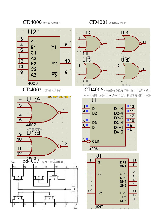
CD4000:双三输入或非门CD4001:四双输入或非门CD4002双四输入或非门CD4006:18位静态移位寄存器//当D1为高(低)时clk给四个脉冲D1+4为高(低),相当于延迟四个脉冲cd4007:双互补对加反相器CD4008:并行进位输出全加器CD4009:六缓相器/转换-倒相CD4010:六缓相器/转换-正相CD4011四2输入端与非门CD4012双4输入端与非门CD4013双主-从D型触发器CD4014 8位串入/并入-串出移位寄存器CD4015双4位串入/并出移位寄存器CD4016四传输门CD4017十进制计数/分配器CD4018可预制1/N计数器//当PE为高时并行输入数据,与clk无关,PE为低时D输入并移位CD4019四与或选择器CD4020 14级串行二进制计数/分频器clk给八个下降沿Q3开始计数CD4021 08位串入/并入-串出移位寄存器当9脚为同时D5-D7并行输入数据且与时钟无关,当其为低电平时从D4数据开始移位,SIN数据迟后六个脉冲CD402八进制计数/分配器CD4023三3输入端与非门CD4024 7级二进制串行计数/分频器CD4025三3输入端或非门CD4026十进制计数/7段译码器当2和15为低3为高时,数码管随脉冲0-1-2…9-02脚为高电平时计数锁存脚5.4.14一般为高显9时5脚为低显2时14脚为低4脚与3脚一至CD4027双J-K触发器CD4028 BCD码十进制译码器当jk同时为1时Qn+1=Qn’CD4029可预置可逆计数器CD4030四异或门当输入全部为低时,只给clk时钟,输出从9到0计数co平时为高输出为0时其为低,当只有10脚为高时给Clk电路从0到9计数,co只在显9时为低。
5脚为高电平则锁存。
1脚为高则并行置数·CD4033 十进制计数/7段译码器CD4034 8位通用总线寄存器CD4035 4位并入/串入-并出/串出移位寄存CD4038三串行加法器CD4040 12级二进制串行计数/分频器CD4041四同相/反相缓冲器脚1为脚3的同相输出,脚2为脚3的反相输出CD4042四锁存D型触发器CD4043 4三态R-S锁存触发器("1"触发) CD4044四三态R-S锁存触发器("0"触发) CD4046锁相环\\见资料CD4047无稳态/单稳态多谐振荡器\\见资料CD4048 4输入端可扩展多功能门\\见资料CD4049六反相缓冲/变换器CD4050六同相缓冲/变换器CD4051八选一模拟开关CD4052双4选1模拟开关6脚为低电平时有效;6脚为低电平时无效CD4053三组二路模拟开关只要A为1,NH CD4054 液晶显示驱动器为低x=x1;若A为0;INH为低不管BCX=x0CD4055 BCD-7段译码/液晶驱动器CD4056液晶显示驱动器当6脚为高电平时输出反码CD4059“N”分频计数器CD4060 14级二进制串行计数/分频器CD4063四位数字比较器CD4066四传输门CD4067 16选1模拟开关CD4068八输入端与非门/与门4069六反相器CD4070四异或门CD4071四2输入端或门CD4072双4输入端或门CD4073三3输入端与门CD4075三3输入端或门CD4076四D寄存器\\见资料CD4077四2输入端异或非门CD4078 8输入端或非门/或门CD4081四2输入端与门CD4082双4输入端与门CD4093四2输入端施密特触发器CD4085双2路2输入端与或非门CD4094 8位移位存储总线寄存器CD4095 3输入端J-K触发器STB为高时则将移位的数据显示出来,STB为低时输出保持不变,移位在工作只是没有显出来,要等到下次STB为高时才显出来,相当于74595的两个时钟CD4096 3输入端J-K触发器CD4098双单稳态触发器CD4099 8位可寻址锁存器CD40105先入先出FI-FD寄存器CD40106六施密特触发器CD40110十进制加/减,计数,锁存,译码驱动CD40160可预置BCD加计数器CD40161可预置4位二进制加计数器CD40162 BCD加法计数器CD40163 4位二进制同步计数器CD40174六锁存D型触发器CD40175四D型触发器CD40192可预置BCD CD40193可预置4位二进制CD40194 4位并入/串入-并加/减计数器(双时钟) 加/减计数器出/串出移位寄存CD4502可选通三态输出六反相/缓冲器CD4503六同相三态缓冲器CD4508双4位锁存D型触发器//12脚为低反相CD4510可预置BCD码加/减计数器CD4511 BCD锁存,7段译码,驱动器CD4512八路数据选择器CD4513 BCD锁存,7段CD4514 4位锁存,4线-16CD4515 4位锁存,4线-16 译码,驱动器(消隐) 线译码器线译码器CD4516可预置4位二进制加/减计数器CD4518双BCD同步加计数器CD4520双4位二进制同步加计数器CD4522可预置BCD同步1/N计数器CD4526可预置4位二进制同步1/N计数器CD4528双单稳态触发器CD4529双四路/单八路模拟开关CD4530双5输入端优势逻辑门CD4532 8位优先编码器CD4538精密双单稳CD4539双四路数据选择器CD4541 可编程序振荡/计时器CD4543BCD七段锁存译码,驱动器CD4553三位BCD计数器CD4555双二进制四选一译码器/分离器CD4556双二进制四选CD4560 "N"BCD加法器CD4584六施密特触发器一译码器/分离器CD4585 4位数值比较器。
40系列CMOS电路型号功能

40193 CMOS 可预制四位二进制计数器
40194 CMOS 4位双向并行存取通用移位寄存器
4020 CMOS 14级二进制串行计数/分频器
40208 CMOS 4×4多端寄存器
4021 CMOS 异步8位并入同步串入/串出寄存器
4022 CMOS 八进制计数器/分频器
4010 CMOS 六缓冲器/转换器(同相)
40100 CMOS 32位双向静态移位寄存器
40101 CMOS 9位奇偶发生器/校验器
40102 CMOS 8位BCD可预置同步减法计数器
40103 CMOS 8位二进制可预置同步减法计数器
40104 CMOS 4位三态输出双向通用移位寄存器
40105 CMOS 先进先出寄存器
40106 CMOS 六施密特触发器
40107 CMOS 2输入双与非缓冲/驱动器
40108 CMOS 4×4多端寄存
40109 CMOS 四三态输出低到高电平移位器
4011 CMOS 四2输入与非门
40110 CMOS 十进制加减计数/译码/锁存/驱动
4035 CMOS 4位并入/并出移位寄存器
4038 CMOS 3位串行负逻辑加法器
4040 CMOS 12级二进制计数/分频器
4041 CMOS 四原码/补码缓冲器
4042 CMOS 四时钟控制 D 锁存器
4043 CMOS 四三态或非 R/S 锁存器
4502 CMOS 可选通六反相缓冲器
4503 CMOS 六三态同相缓冲器
4504 CMOS 六TTL-CMOS电平移位器
4506 CMOS 双二组2输入可扩展与或非门
4023 CMOS 三3输入与非门

October 1987Revised June 1999CD4023BC Buffered Triple 3-Input NAND Gate © 1999 Fairchild Semiconductor Corporation DS005956.prf CD4023BCBuffered Triple 3-Input NAND GateGeneral DescriptionThese triple gates are monolithic complementary MOS(CMOS) integrated circuits constructed with N- and P-channel enhancement mode transistors. They have equalsource and sink current capabilities and conform to stan-dard B series output drive. The devices also have bufferedoutputs which improve transfer characteristics by providingvery high gain. All inputs are protected against static dis-charge with diodes to V DD and V SS.Featuress Wide supply voltage range: 3.0V to 15Vs High noise immunity:0.45 V DD (typ)s Low power TTL compatibility:fan out of 2 driving 74L or 1 driving 74LSs5V–10V–15V parametric ratingss Symmetrical output characteristicss Maximum input leakage 1 µA at 15V over fulltemperature rangeOrdering Code:Devices also available in T ape and Reel. Specify by appending the suffix letter “X” tot he ordering code.Connection DiagramTop ViewBlock Diagram1/3 Device Shown*All Inputs Protected by Standard CMOS Input Protection Circuit.Order Number Package Number Package DescriptionCD4023BCM M14B14-Lead Small Outline Integrated Circuit (SOIC), JEDEC MS-013, 0.300 WideCD4023BCS M14D14-Lead Small Outline Package (SOP), EIAJ TYPE II, 5.3mm WideCD4023BCN N14A14-Lead Plastic Dual-In-Line Package (PDIP), JEDEC MS-001, 0.300 Wide 2C D 4023B CAbsolute Maximum Ratings (Note 1)(Note 2)Recommended Operating ConditionsNote 1: “Absolute Maximum Ratings” are those values beyond which the safety of the device cannot be guaranteed; they are not meant to imply that the devices should be operated at these limits. The table of “Recom-mended Operating Conditions” and “Electrical Characteristics” provides conditions for actual device operation.Note 2: V SS = 0V unless otherwise specified.DC Electrical Characteristics (Note 3)Note 3: V SS = 0V unless otherwise specified.Note 4: I OH and I OL are tested one output at a time.DC Supply Voltage (V DD )−0.5V DC to +18V DC Input Voltage (V IN )−0.5V DC to V DD +0.5V DCStorage Temp. Range (T S )−65°C to +150°CPower Dissipation (P D )Dual-In-Line 700 mW Small Outline 500 mWLead Temperature (T L )(Soldering, 10 seconds)260°C DC Supply Voltage (V DD )5V DC to 15 V DC Input Voltage (V IN )0 V DC to V DD V DC Operating Temperature Range (T A )−40°C to +85°CSymbol ParameterConditions−40°C +25°C +85°C Units MinTyp MinTyp Max MinMax I DDQuiescent Device CurrentV DD = 5V 1.00.004 1.07.5µAV DD = 10V 2.00.005 2.015V DD = 15V4.00.006 4.030V OLLOW Level Output Voltage V DD = 5V0.0500.050.05VV DD = 10V 0.0500.050.05V DD = 15V0.0500.050.05V OHHIGH Level Output Voltage V DD = 5V4.95 4.955 4.95VV DD = 10V 9.959.95109.95V DD = 15V14.9514.951514.95V ILLOW Level Input VoltageV DD =5V, V O =4.5V 1.52 1.5 1.5VV DD =10V, V O =9.0V |I O |<1µA3.04 3.0 3.0V DD =15V, V O =13.5V4.06 4.0 4.0V IHHIGH Level Input VoltageV DD =5V, V O =0.5V 3.53.53 3.5VV DD =10V, V O =1.0V |I O |<1µA7.07.067.0V DD =15V, V O =1.5V11.011.0911.0I OLLOW Level Output Current V DD =5V, V O = 0.4V 0.520.440.880.36mA(Note 4)V DD = 10V, V O = 0.5V 1.3 1.1 2.20.90V DD = 15V, V O = 1.5V3.6 3.08 2.4I OHHIGH Level Output Current V DD = 5V, V O = 4.6V −0.52−0.44−0.88−0.36mA(Note 4)V DD = 10V, V O = 9.5V −1.3−1.1−2.2−0.90V DD = 15V, V O = 13.5V −3.6−3.0−8−2.4I INInput CurrentV DD = 15V, V IN = 0V −0.3−10−5−0.3−1.0µAV DD = 15V, V IN = 15V0.310−50.3 1.0CD4023BCAC Electrical Characteristics (Note 5)T A = 25°C, C L = 50 pF, R L = 200k, unless otherwise specified Note 5: AC Parameters are guaranteed by DC correlated testing.Note 6: C PD determines the no load AC power consumption of any CMOS device. For complete explanation, see Family Characteristics Application Note AN-90.Symbol ParameterConditionsMinTyp Max Units t PHLPropagation Delay, HIGH-to-LOW LevelV DD = 5V 130250nsV DD = 10V 60100V DD = 15V4070t PLHPropagation Delay, LOW-to-HIGH LevelV DD = 5V 110250ns V DD = 10V 50100V DD = 15V3570t THL ,Transition TimeV DD = 5V 90200ns t TLH V DD = 10V 50100V DD = 15V 4080C IN Average Input CapacitanceAny Input 57.5pF C PDPower Dissipation Capacity (Note 6)Any Gate17pF 4C D 4023B CPhysical Dimensions inches (millimeters) unless otherwise noted14-Lead Small Outline Integrated Circuit (SOIC), JEDEC MS-013, 0.300 WidePackage Number M14B14-Lead Small Outline Package (SOP), EIAJ TYPE II, 5.3mm WidePackage Number M14DFairchild does not assume any responsibility for use of any circuitry described, no circuit patent licenses are implied and Fairchild reserves the right at any time without notice to change said circuitry and specifications.CD4023BC Buffered Triple 3-Input NAND GateLIFE SUPPORT POLICYFAIRCHILD’S PRODUCTS ARE NOT AUTHORIZED FOR USE AS CRITICAL COMPONENTS IN LIFE SUPPORT DEVICES OR SYSTEMS WITHOUT THE EXPRESS WRITTEN APPROVAL OF THE PRESIDENT OF FAIRCHILD SEMICONDUCTOR CORPORATION. As used herein:1.Life support devices or systems are devices or systemswhich, (a) are intended for surgical implant into thebody, or (b) support or sustain life, and (c) whose failureto perform when properly used in accordance withinstructions for use provided in the labeling, can be rea-sonably expected to result in a significant injury to the user.2. A critical component in any component of a life support device or system whose failure to perform can be rea-sonably expected to cause the failure of the life support device or system, or to affect its safety or Physical Dimensions inches (millimeters) unless otherwise noted (Continued)14-Lead Plastic Dual-In-Line Package (PDIP), JEDEC MS-001, 0.300 WidePackage Number N14A。
_CD系列芯片功能大全

_CD系列芯⽚功能⼤全**********************************************************************CD系列门电路CD4000 双3输⼊端或⾮门CD4001 四2输⼊端或⾮门CD4002 双4输⼊端或⾮门CD4007 双互补对加反向器CD4009 六反向缓冲/变换器CD4011 四2输⼊端与⾮门CD4012 双4输⼊端与⾮门CD4023 三2输⼊端与⾮门CD4025 三2输⼊端与⾮门CD4030 四2输⼊端异或门CD4041 四同相/反向缓冲器CD4048 8输⼊端可扩展多功能门CD4049 六反相缓冲/变换器CD4050 六同相缓冲/变换器CD4068 8输⼊端与门/与⾮门CD4069 六反相器CD4070 四2输⼊异或门CD4071 四2输⼊端或门CD4072 双4输⼊端或门CD4073 三3输⼊端与门CD4075 三3输⼊端或门CD4077 四异或⾮门CD4078 8输⼊端与⾮门/或门CD4081 四2输⼊端与门CD4082 双4输⼊端与⾮门CD4085 双2路2输⼊端与或⾮门CD4086 四2输⼊端可扩展与或⾮门CD40104 TTL⾄⾼电平CMOS转换器CD40106 六施密特触发器CD40107 双2输⼊端与⾮缓冲/驱动器CD40109 四低-⾼电平位移器CD4501 三多输⼊门CD4052 六反向缓冲器(三态输出)CD4503 六同相缓冲器(三态输出)CD4504 6TTL或CMOS同级移相器CD4506 双可扩展AIO门CD4507 四异或门CD4519 4位与/或选择器CD4530 双5输⼊多数逻辑门CD4572 四反向器加⼆输⼊或⾮门加⼆输⼊与⾮门CD4599 8位可寻址锁存器**********************************************************************触发器CD4013 双D触发器CD4027 双JK触发器CD4042 四锁存D型触发器CD4043 四三态R-S锁存触发器(“1”触发)CD4044 四三态R-S锁存触发器(“0”触发)CD4047 单稳态触发/⽆稳多谐振荡器CD4093 四2输⼊端施密特触发器CD4098 双单稳态触发器CD4099 8位可寻址锁存器CD4508 双4位锁存触发器CD4528 双单稳态触发器(与CD4098管脚相同,只是3、13脚复位开关为⾼电平有效)CD4538 精密单稳多谐振荡器CD4583 双施密特触发器CD4584 六施密特触发器CD4599 8位可寻址锁存器**********************************************************************计数器CD4017 ⼗进制计数/分配器CD4020 14位⼆进制串⾏计数器/分频器CD4022 ⼋进制计数/分配器CD4024 7位⼆进制串⾏计数器/分频器CD4029 可预置数可逆计数器(4位⼆进制或BCD码)CD4040 12⼆进制串⾏计数器/分频器CD4045 12位计数/缓冲器CD4059 四⼗进制N分频器CD4060 14⼆进制串⾏计数器/分频器和振荡器CD4095 3输⼊端J-K触发器(相同J-K输⼊端)CD4096 3输⼊端J-K触发器(相反和相同J-K输⼊端)CD40110 ⼗进制加/减计数/锁存/7端译码/驱动器CD40160 可预置数BCD加计数器(异步复位)CD40161 可预置数4位⼆进制加计数器(R⾮=0时,CP上脉冲复位)(异步复位)CD40162 可预置数BCD加计数器(同步复位)CD40163 可预置数4位⼆进制加计数器(R⾮=0时,CP上脉冲复位)(同步复位)CD40192 可预置数BCD加/减计数器CD40193 可预置数4位⼆进制加/减计数器CD4510 可预置BCD加/减计数器CD4516 可预置4位⼆进制加/减计数器CD4518 双BCD同步加计数器CD4520 双同步4位⼆进制加计数器CD4521 24级频率分频器CD4522 可预置数BCD同步1/N加计数器CD4526 可预置数4位⼆进制同步1/N加计数器CD4534 实时与译码计数器CD4536 可编程定时器CD4541 可编程定时器CD4553 3数字BCD计数器CD4568 相位⽐较器/可编程计数器CD4569 双可预置BCD/⼆进制计数器CD4597 8位总线相容计数/锁存器CD4598 8位总线相容可建地址锁存器**********************************************************************译码器CD4511 BCD锁存/7段译码器/驱动器CD4514 4位锁存/4-16线译码器CD4515 4位锁存/4-16线译码器(负逻辑输出)CD4026 ⼗进制计数/7段译码器(适⽤于时钟计时电路,利⽤C端的功能可⽅便的实现60或12分频)CD4028 BCD-⼗进制译码器CD4033 ⼗进制计数/7段译码器CD4054 4位液晶显⽰驱动CD4055 BCD-7段码/液晶驱动CD4056 BCD-7段码/驱动CD40102 8位可预置同步减法计时器(BCD)CD40103 8位可预置同步减法计时器(⼆进制)CD4513 BCD-锁存/7端译码/驱动器(⽆效“0”不显)CD4514 4位锁存/4线—16线译码器(输出“1”)CD4515 4位锁存/4线—16线译码器(输出“0”)CD4543 BCD-锁存/7段译码/驱动器CD4544 BCD-锁存/7段译码/驱动器——波动闭锁CD4547 BCD-锁存/7段译码/⼤电流驱动器CD4555 双⼆进制4选1译码器/分离器(输出“1”)CD4556 双⼆进制4选1译码器/分离器(输出“0”)CD4558 BCD-7段译码CD4555 双⼆进制4选1译码器/分离器CD4556 双⼆进制4选1译码器/分离器(负逻辑输出)**********************************************************************移位寄存器CD4006 18位串⼊—串出移位寄存器CD4014 8位串⼊/并⼊—串出移位寄存器CD4015 双4位串⼊—并出移位寄存器CD4021 8位串⼊/并⼊—串出移位寄存器CD4031 64位移位寄存器CD4034 8位通⽤总线寄存器CD4035 4位串⼊/并⼊—串出/并出移位寄存器CD4076 4线D型寄存器CD4094 8位移位/存储总线寄存器CD40100 32位左移/右移CD40105 先进先出寄存器CD40108 4×4多端⼝寄存器阵列CD40194 4位并⼊/串⼊—并出/串出移位寄存器(左移/右移)CD40195 4位并⼊/串⼊—并出/串出移位寄存器CD4517 64位移位寄存器CD45490 连续的近似值寄存器CD4562 128位静态移位寄存器CD4580 4×4多端寄存器**********************************************************************模拟开关和数据选择器CD4016 四联双向开关CD4019 四与或选择器【Qn=(An*Ka)+(Bn*Kb)】CD4051 单⼋路模拟开关CD4052 双4路模拟开关CD4053 三2路模拟开关CD4066 四双向模拟开关CD4067 单⼗六路模拟开关CD4097 双⼋路模拟开关CD40257 四2选1数据选择器CD4512 ⼋路数据选择器CD4529 双四路/单⼋路模拟开关CD4539 双四路数据选择器CD4551 四2通道模拟多路传输**********************************************************************运算电路CD4008 4位超前进位全加器CD4019 四与或选择器【Qn=(An*Ka)+(Bn*Kb)】CD4527 BCD⽐例乘法器CD4032 三路串联加法器CD4038 三路串联加法器(负逻辑)CD4063 四位量级⽐较器CD4070 四2输⼊异或门CD4585 4位数值⽐较器CD4089 4位⼆进制⽐例乘法器CD40101 9位奇偶发⽣器/校验器CD4527 BCD⽐例乘法器CD4531 12位奇偶数CD4559 逐次近似值码器CD4560 “N”BCD加法器CD4561 “9”求补器CD4581 4位算术逻辑单元CD4582 超前进位发⽣器CD4585 4位数值⽐较器**********************************************************************存储器CD4049 4字×8位随机存取存储器CD4505 64×1位RAMCD4537 256×1静态随机存取存储器CD4552 256位RAM**********************************************************************特殊电路CD4046 锁相环集成电路CD4532 8位优先编码器CD4500 ⼯业控制单元CD4566 ⼯业时基发⽣器CD4573 可预置运算放⼤器CD4574 ⽐较器、线性、双对双运放CD4575 双/双预置运放/⽐较器CD4597 8位总线相容计数/锁存器CD4598 8位总线相容可建地址锁存器。
IC集成电路型号大全及40系列芯片功能大全
CD4000 双3输入端或非门单非门CD4001 四2输入端或非门CD4002 双4输入端或非门CD4006 18位串入/串出移位寄存器CD4007 双互补对加反相器CD4008 4位超前进位全加器CD4009 六反相缓冲/变换器CD4010 六同相缓冲/变换器CD4011 四2输入端与非门CD4012 双4输入端与非门CD4013 双主-从D型触发器CD4014 8位串入/并入-串出移位寄存器CD4015 双4位串入/并出移位寄存器CD4016 四传输门CD4017 十进制计数/分配器CD4018 可预制1/N计数器CD4019 四与或选择器CD4020 14级串行二进制计数/分频器CD4021 08位串入/并入-串出移位寄存器CD4022 八进制计数/分配器CD4023 三3输入端与非门CD4024 7级二进制串行计数/分频器CD4025 三3输入端或非门CD4026 十进制计数/7段译码器CD4027 双J-K触发器CD4028 BCD码十进制译码器CD4029 可预置可逆计数器CD4030 四异或门CD4031 64位串入/串出移位存储器CD4032 三串行加法器CD4033 十进制计数/7段译码器CD4034 8位通用总线寄存器CD4035 4位并入/串入-并出/串出移位寄存CD4038 三串行加法器CD4040 12级二进制串行计数/分频器CD4041 四同相/反相缓冲器CD4042 四锁存D型触发器CD4043 三态R-S锁存触发器("1"触发) CD4044 四三态R-S锁存触发器("0"触发) CD4046 锁相环CD4047 无稳态/单稳态多谐振荡器CD4048 四输入端可扩展多功能门CD4049 六反相缓冲/变换器CD4050 六同相缓冲/变换器CD4051 八选一模拟开关CD4052 双4选1模拟开关CD4053 三组二路模拟开关CD4054 液晶显示驱动器CD4055 BCD-7段译码/液晶驱动器CD4056 液晶显示驱动器CD4059 “N”分频计数器 NSC/TICD4060 14级二进制串行计数/分频器CD4063 四位数字比较器CD4066 四传输门CD4067 16选1模拟开关CD4068 八输入端与非门/与门CD4069 六反相器CD4070 四异或门CD4071 四2输入端或门CD4072 双4输入端或门CD4073 三3输入端与门CD4075 三3输入端或门CD4076 四D寄存器CD4077 四2输入端异或非门CD4078 8输入端或非门/或门CD4081 四2输入端与门CD4082 双4输入端与门CD4085 双2路2输入端与或非门CD4086 四2输入端可扩展与或非门CD4089 二进制比例乘法器CD4093 四2输入端施密特触发器CD4095 三输入端J-K触发器CD4096 三输入端J-K触发器CD4097 双路八选一模拟开关CD4098 双单稳态触发器CD4099 8位可寻址锁存器CD40100 32位左/右移位寄存器CD40101 9位奇偶较验器CD40102 8位可预置同步BCD减法计数器CD40103 8位可预置同步二进制减法计数器CD40104 4位双向移位寄存器CD40105 先入先出FI-FD寄存器CD40106 六施密特触发器CD40107 双2输入端与非缓冲/驱动器CD40108 4字×4位多通道寄存器CD40109 四低-高电平位移器CD40110 十进制加/减,计数,锁存,译码驱动CD40147 10-4线编码器CD40160 可预置BCD加计数器CD40161 可预置4位二进制加计数器CD40162 BCD加法计数器CD40163 4位二进制同步计数器CD40174 六锁存D型触发器CD40175 四D型触发器CD40181 4位算术逻辑单元/函数发生器CD40182 超前位发生器CD40192 可预置BCD加/减计数器(双时钟) CD40193 可预置4位二进制加/减计数器CD40194 4位并入/串入-并出/串出移位寄存CD40195 4位并入/串入-并出/串出移位寄存CD40208 4×4多端口寄存器CD4501 4输入端双与门及2输入端或非门CD4502 可选通三态输出六反相/缓冲器CD4503 六同相三态缓冲器CD4504 六电压转换器CD4506 双二组2输入可扩展或非门CD4508 双4位锁存D型触发器CD4510 可预置BCD码加/减计数器CD4511 BCD锁存,7段译码,驱动器CD4512 八路数据选择器CD4513 BCD锁存,7段译码,驱动器(消隐) CD4514 4位锁存,4线-16线译码器CD4515 4位锁存,4线-16线译码器CD4516 可预置4位二进制加/减计数器CD4517 双64位静态移位寄存器CD4518 双BCD同步加计数器CD4519 四位与或选择器CD4520 双4位二进制同步加计数器CD4521 24级分频器CD4522 可预置BCD同步1/N计数器CD4526 可预置4位二进制同步1/N计数器CD4527 BCD比例乘法器CD4528 双单稳态触发器CD4529 双四路/单八路模拟开关CD4530 双5输入端优势逻辑门CD4531 12位奇偶校验器CD4532 8位优先编码器CD4536 可编程定时器CD4538 精密双单稳CD4539 双四路数据选择器CD4541 可编程序振荡/计时器CD4543 BCD七段锁存译码,驱动器CD4544 BCD七段锁存译码,驱动器CD4547 BCD七段译码/大电流驱动器CD4549 函数近似寄存器CD4551 四2通道模拟开关CD4553 三位BCD计数器CD4555 双二进制四选一译码器/分离器CD4556 双二进制四选一译码器/分离器CD4558 BCD八段译码器CD4560 "N"BCD加法器CD4561 "9"求补器CD4573 四可编程运算放大器CD4574 四可编程电压比较器CD4575 双可编程运放/比较器CD4583 双施密特触发器CD4584 六施密特触发器CD4585 4位数值比较器CD4599 8位可寻址锁存器CD22100 4×4×1交叉点开关0206A 天线开关集成电路03VFG9 发射压控振荡集成电路1021AC 发射压控振荡集成电路1097C 升压集成电路140N 电源取样比较放大集成电路 14DN363 伺服控制集成电路15105 充电控制集成电路15551 管理卡升压集成电路1710 视频信号处理集成电路1N706 混响延时集成电路20810-F6096 存储集成电路2252B 微处理集成电路2274 延迟集成电路24C01ACEA 存储集成电路24C04 存储集成电路24C64 码片集成电路24LC16B 存储集成电路24LC65 电可改写编程只读存储集成电路 27C1000PC-12 存储集成电路27C2000QC-90 存储集成电路27C20T 存储集成电路27C512 电可改写编程只读存储集成电路 2800 红外遥控信号接收集成电路28BV64 码片集成电路28F004 版本集成电路31085 射频电源集成电路32D54 电源、音频信号处理集成电路1732D75 电源、音频信号处理集成电路32D92 电源中频放大集成电路4066B 电子开关切换集成电路4094 移位寄存串入、并出集成电路424260SDJ 存储集成电路4260 动态随机存储集成电路4270351/91B9905 中频放大集成电路4370341/90M9919 中频处理集成电路4464 存储集成电路4558 双运算放大集成电路4580D 双运算放大集成电路47C1638AN-U337 微处理集成电路47C1638AU-353 微处理集成电路47C432GP 微处理集成电路47C433AN-3888 微处理集成电路49/4CR1A 中频放大集成电路5101 天线开关集成电路5G052 发光二极管四位显示驱动集成电路 5G24 运算放大集成电路5W01 双运算放大集成电路649/CRIA70612 中频放大集成电路673/3CR2A 多模转换集成电路74122 可重触发单稳态集成电路74HC04 逻辑与非门集成电路74HC04D 六反相集成电路74HC123 单稳态集成电路74HC125 端口功能扩展集成电路74HC14N 六反相集成电路74HC157A 多路转换集成电路1874HC245 总线收发集成电路74HC32 或门四2输入集成电路74HC374八D 触发集成电路74HC573D 存储集成电路74HCT157 多路转换双输入集成电路74HCT4046A 压控振荡集成电路74HCT4538D 单稳态集成电路74HCT4538N 触发脉冲集成电路74HCT86D 异或门四2输入集成电路74HCU04 与非门集成电路74LS125 端口功能扩展集成电路74LS373 锁存集成电路74LS393 计数双四位二进制集成电路74LS74双D 触发集成电路78014DFP 系统控制处理集成电路811N 伴音阻容偏置集成电路83D33 压控振荡集成电路85712 场扫描信号校正处理集成电路 85713 行扫描信号校正集成电路87C52 微处理集成电路87CK38N-3584 微处理集成电路87CK38N-3627 微处理集成电路89C52 系统控制处理集成电路89C55 系统控制处理集成电路93C66 电可改写编程只读存储集成电路 93LC56 电可改写编程存储集成电路9821K03 系统控制集成电路A1642P 背景歌声消除集成电路A701 红外遥控信号接收集成电路A7950 场频识别集成电路19A8772AN 色差信号延迟处理集成电路A9109 功率放大集成电路AAB 电源集成电路ACA650 色度信号解调集成电路ACFP2 色度、亮度信号分离集成电路 ACP2371 多伴音、多语言改善集成电路 ACVP2205 色度、亮度信号分离集成电路 AD1853 立体声数/模转换集成电路AD1858 音频解调集成电路AD722 视频编码集成电路ADC2300E 音频数/模转换集成电路ADC2300J 音频数/模转换集成电路ADC2310E 音频数/模转换集成电路ADV7172 视频编码集成电路ADV7175A 视频编码集成电路AE31201 频率显示集成电路AJ7080 射频调制集成电路AK4321-VF-E1 音频数/模转换集成电路AN1319 双高速电压比较集成电路AN1358S 双运算放大集成电路AN1393 双运算放大集成电路AN1431T 稳压电源集成电路AN1452 音频前置放大集成电路AN1458S 双运算放大集成电路AN206 伴音中频及前置放大集成电路AN222 自动频率控制集成电路AN236 副载波信号处理集成电路AN239Q 图像、伴音中频放大集成电路AN247P 图像中频放大、AGC控制集成电路 AN253P 调频/调幅中频放大集成电路20AN262 音频前置放大集成电路AN2661NK 视频信号处理集成电路AN2663K 视频信号处理集成电路AN272 音频功率放大集成电路AN2751FAP 视频信号处理集成电路AN281 色度解码集成电路AN2870FC 多功能控制集成电路AN295 行、场扫描信号处理集成电路AN301 伺服控制集成电路AN305 视频自动增益控制集成电路AN306 色度自动相位控制集成电路AN318 直流伺服控制集成电路AN320 频率控制、调谐显示驱动集成电路 AN3215K 视频信号处理集成电路AN3215S 视频信号处理集成电路AN3224K 磁头信号记录放大集成电路AN3248NK 亮度信号记录、重放处理集成电路 AN331 视频信号处理集成电路AN3311K 磁头信号放大集成电路AN3313 磁头信号放大集成电路AN3321S 录像重放信号处理集成电路AN3331K 磁头信号处理集成电路AN3337NSB 磁头信号放大集成电路AN3380K 磁头信号处理集成电路AN3495K 色度、亮度信号降噪集成电路AN355 伴音中频放大、检波集成电路AN3581S 视频驱动集成电路AN366 调频/调幅中频放大集成电路AN3791 移位控制集成电路21AN3792 磁鼓伺服控制接口集成电路AN3795 主轴伺服控制接口集成电路AN3814K 电机驱动集成电路AN4265 音频功率放大集成电路AN4558 运算放大集成电路AN5010 电子选台集成电路AN5011 电子选台集成电路AN5015K 电子选台集成电路AN5020 红外遥控信号接收集成电路AN5025S 红外遥控信号接收集成电路AN5026K 红外遥控信号接收集成电路AN5031 电调谐控制集成电路AN5034 调谐控制集成电路AN5036 调谐控制集成电路AN5043 调谐控制集成电路AN5071 频段转换集成电路AN5095K 电视信号处理集成电路AN5110 图像中频放大集成电路AN5130 图像中频、视频检波放大集成电路AN5138NK 图像、伴音中频放大集成电路AN5156K 电视信号处理集成电路AN5177NK 图像、伴音中频放大集成电路AN5179K 图像、伴音中频放大集成电路AN5183K 中频信号处理集成电路AN5195K 中频、色度、扫描信号处理集成电路AN5215 伴音信号处理集成电路AN5520 伴音中频放大及鉴频集成电路AN5222 伴音中频放大集成电路AN5250 伴音中频放大、鉴频及功率放大集成电路 AN5262 音频前置放大集成电路22AN5265 音频功率放大集成电路AN5270 音频功率放大集成电路AN5273 双声道音频功率放大集成电路AN5274 双声道音频功率放大集成电路AN5275 中置、3D放大集成电路AN5285K 双声道前置放大集成电路AN5312 视频、色度信号处理集成电路AN5313NK 视频、色度信号处理集成电路AN5342 图像水平轮廓校正集成电路AN5342FB 水平清晰度控制集成电路AN5344FBP 色度信号处理集成电路AN5348K 人工智能信号处理集成电路AN5385K 色差信号放大集成电路AN5410 行、场扫描信号处理集成电路AN5421 同步检测集成电路AN5422 行、场扫描信号处理集成电路AN5512 场扫描输出集成电路AN5515 场扫描输出集成电路AN5521 场扫描输出集成电路AN5532 场扫描输出集成电路AN5534 场扫描输出集成电路AN5551 枕形校正集成电路AN5560 场频识别集成电路AN5600K 中频、亮度、色度及扫描信号处理集成电路 AN5601K 视频、色度、同步信号处理集成电路AN5607K 视频、色度、行场扫描信号处理集成电路 AN5615 视频信号处理集成电路AN5620X 色度信号处理集成电路AN5621 场扫描输出集成电路23AN5625 色度信号处理集成电路AN5633K 色度信号处理集成电路AN5635 色度解码集成电路AN5635NS 色度解码集成电路AN5637 色度解码、亮度延迟集成电路AN5650 同步信号分离集成电路AN5682K 基色电子开关切换集成电路AN5693K 视频、色度、行场扫描信号处理集成电路 AN5712 图像中频放大、AGC控制集成电路AN5722 图像中频放大、检波集成电路AN5732 伴音中频放大、鉴频集成电路AN5743 音频功率放大集成电路AN5750 行自动频率控制及振荡集成电路AN5757S 行扫描电源电压控制集成电路AN5762 场扫描振荡、输出集成电路AN5764 光栅水平位置控制集成电路AN5765 电源稳压控制集成电路AN5767 同步信号处理集成电路AN5768 光栅倾斜校正控制集成电路AN5790N 行扫描信号处理集成电路AN5791 同步脉冲相位与脉宽调整集成电路 AN5803 双声道立体声解调集成电路AN5836 双声道前置放大集成电路AN5858K 视频信号控制集成电路AN5862 视频信号控制集成电路AN5862S-E1 视频信号开关控制集成电路AN5870K 模拟信号切换集成电路AN5891K 音频信号处理集成电路AN614 行枕形校正集成电路24AN6210 双声道前置放大集成电路AN6306S 亮度信号处理集成电路AN6308 模拟电子开关集成电路AN6327 视频重放信号处理集成电路AN6341N 伺服控制集成电路AN6342N 基准分频集成电路AN6344 伺服控制集成电路AN6345 分频集成电路AN6346N 磁鼓伺服控制集成电路AN6350 磁鼓伺服控制集成电路AN6357N 主轴接口集成电路AN6361N 色度信号处理集成电路AN6367NK 色度信号处理集成电路AN6371S 自动相位控制集成电路AN6387 电机伺服控制集成电路AN6550 卡拉OK音频放大集成电路AN6554 四运算放大集成电路AN6561 双运算放大集成电路AN6562SG 双运算放大集成电路AN6609N 电机驱动集成电路AN6612 电机稳速控制集成电路AN6650 电机速度控制集成电路AN6651 电机速度控制集成电路AN6652 电机稳速控制集成电路AN6875 发光二极管五位显示驱动集成电路 AN6877 发光二极管七位显示驱动集成电路 AN6884 发光二极管五位显示驱动集成电路 AN6886 发光二极管五位显示驱动集成电路 AN6888 发光二极管显示驱动集成电路AN6914 双电压比较集成电路25AN7085N5 单片录、放音集成电路AN7105 双声道音频功率放大集成电路AN7106K 双声道音频功率放大集成电路AN7108 单片立体声放音集成电路AN710S 单片放音集成电路AN7110E 音频功率放大集成电路AN7114 音频功率放大集成电路AN7116 音频功率放大集成电路AN7118 双声道音频功率放大集成电路AN7118S 双声道音频功率放大集成电路AN7120 音频功率放大集成电路AN7124 双声道音频功率放大集成电路AN7145 双声道音频功率放大集成电路AN7148 双声道音频功率放大集成电路AN7158N 音频功率放大7.5W×2集成电路 AN7161N 音频功率放大集成电路AN7164 双声道音频功率放大集成电路AN7171NK 音频功率放大集成电路AN7205 调频/调谐及高频放大集成电路 AN7220 调频/调幅中频放大集成电路AN7222 调频/调幅中频放大集成电路AN7223 调频/调幅中频放大集成电路AN7226 调频/调幅中频放大集成电路AN7256 调频/调谐及中频放大集成电路 AN7311 双声道前置放大集成电路AN7312 双声道前置放大集成电路AN7315 双声道前置放大集成电路AN7315S 双声道前置放大集成电路AN7320 音频前置放大集成电路AN7396K 双声道前置放大集成电路26AN7397K 双声道前置放大集成电路AN7410 调频立体声多路解码集成电路AN7414 调频立体声解码集成电路AN7420N 调频立体声解码集成电路AN7470 调频立体声解码集成电路AN7805 三端电源稳压+5V/1A集成电路 AN7806 三端电源稳压+6V/1A集成电路 AN7807 三端电源稳压+7V/1A集成电路 AN7808 三端电源稳压+8V/1A集成电路 AN7809 电源稳压+9V/1A集成电路AN7810 三端电源稳压+10V/1A集成电路 AN7812 三端电源稳压+12V/1A集成电路 AN7815 三端电源稳压+15V/1A集成电路 AN7818 三端电源稳压+18V/1A集成电路AN7824 三端电源稳压+24V/1A集成电路AN78L05 三端电源稳压+5V/0.1A集成电路AN78L06 三端电源稳压+6V/0.1A集成电路AN78L08 三端电源稳压+8V/0.1A集成电路AN78L09 三端电源稳压+9V/0.1A集成电路AN78L10 三端电源稳压+10V/0.1A集成电路 AN78L12 三端电源稳压+12V/0.1A集成电路 AN78L15 三端电源稳压+15V/0.1A集成电路 AN78L18 三端电源稳压+18V/0.1A集成电路 AN78L20 三端电源稳压+20V/0.1A集成电路 AN78L24 三端电源稳压+24V/0.1A集成电路 AN78M05 三端电源稳压+5V/0.5A集成电路AN78M06 三端电源稳压+6V/0.5A集成电路AN78M08 三端电源稳压+8V/0.5A集成电路AN78M09 三端电源稳压+9V/0.5A集成电路27AN78M10 三端电源稳压+10V/0.5A集成电路 AN78M12 三端电源稳压+12V/0.5A集成电路 AN78M15 三端固定式稳压+15V/0.5A集成电路 AN78M18 三端电源稳压+18V/0.5A集成电路 AN78M20 三端电源稳压+20V/0.5A集成电路 AN78M24 三端电源稳压+24V/0.5A集成电路 AN7905 三端电源稳压-5V/1A集成电路AN7906 三端电源稳压-6V/1A集成电路AN7908T 三端电源稳压-8V/1A集成电路AN7909T 三端电源稳压-9V/1A集成电路AN7910T 三端电源稳压-10V/1A集成电路AN7912 三端电源稳压-12V/1A集成电路AN7915 三端电源稳压-15V/1A集成电路AN7918 三端电源稳压-18V/1A集成电路AN7920 三端电源稳压-20V/1A集成电路AN7924 三端电源稳压-24V/1A集成电路AN79L05 三端电源稳压-5V/0.1A集成电路AN79L06 三端电源稳压-6V/0.1A集成电路AN79L08 三端电源稳压-8V/0.1A集成电路AN79L09 三端电源稳压-9V/0.1A集成电路AN79L10 三端电源稳压-10V/0.1A集成电路 AN79L12 三端电源稳压-12V/0.1A集成电路 AN79L15 三端电源稳压-15V/0.1A集成电路 AN79L18 三端电源稳压-18V/0.1A集成电路 AN79L20 三端电源稳压-20V/0.1A集成电路 AN79L24 三端电源稳压-24V/0.1A集成电路 AN79M05 三端电源稳压-5V/0.5A集成电路AN79M08 三端电源稳压-8V/0.5A集成电路 AN79M09 三端电源稳压-9V/0.5A集成电路28AN79M10 三端电源稳压-10V/0.5A集成电路 AN79M12 三端电源稳压-12V/0.5A集成电路 AN79M15 三端电源稳压-15V/0.5A集成电路 AN79M18 三端电源稳压-18V/0.5A集成电路 AN79M20 三端电源稳压-20V/0.5A集成电路 AN79M24 三端电源稳压-24V/0.5A集成电路 AN8028 自激式开关电源控制集成电路AN8270K 主轴电机控制集成电路AN8280 电机驱动集成电路AN8281S 电机驱动集成电路AN8290S 主轴电机驱动集成电路AN8355S 条形码扫描接收集成电路AN8370S 光电伺服控制集成电路AN8373S 射频伺服处理集成电路AN8375S 伺服处理集成电路AN8389S-E1 电机驱动集成电路AN8480NSB 主轴电机驱动集成电路AN8481SB-E1 主轴电机驱动集成电路AN8482SB 主轴电机驱动集成电路AN8623FBQ 主轴伺服处理集成电路AN8788FB 电机驱动集成电路AN8802CE1V 伺服处理集成电路AN8813NSBS 主轴电机驱动集成电路AN8819NFB 伺服驱动、直流交换集成电路AN8824FBQ 前置放大集成电路AN8825NFHQ-V 聚焦、循迹误差处理集成电路AN8831SC 视频预视放集成电路AN8832SB-E1 射频放大、伺服处理集成电路AN8837SB-E1 伺服处理集成电路AN89C2051-24PC 微处理集成电路29APU2400U 音频信号处理集成电路APU2470 音频信号处理集成电路AS4C14405-60JC 动态随机存储1M×4集成电路AS4C256K16ED-60JC 存储集成电路ASD0204-015 图文控制集成电路ASD0204GF--3BA显示控制集成电路AT24C08 存储集成电路AT24C08A 存储集成电路AT24C256-10CI 码片集成电路AT27C010 电可改写编程只读存储集成电路 AT27C020 存储集成电路ATMEL834 存储集成电路AVM-1 视频信号处理厚膜集成电路AVM-2 音频信号处理厚膜集成电路AVSIBCP08 倍压整流切换集成电路B0011A 存储集成电路B1218 电子快门控制集成电路BA033T 三端电源稳压+3.3V集成电路 BA10324 四运算放大集成电路BA10393N 双运算放大集成电路BA1102F 杜比降噪处理集成电路BA1106F 杜比降噪处理集成电路BA12ST 电源稳压集成电路BA1310 调频立体声解码集成电路BA1332L 调频立体声解码集成电路BA1350 调频立体声解码集成电路BA1351 调频立体声解码集成电路BA1356 调频立体声解码集成电路BA1360 调频立体声解码集成电路BA15218N 双运算放大集成电路30BA225 可触发双单稳态振荡集成电路 BA302 音频前置放大集成电路BA311 音频前置放大集成电路BA313 音频前置放大集成电路BA3283 单片放音集成电路BA328F 双声道前置放大集成电路BA329 双声道前置放大集成电路BA3304F 录放音前置均衡放大集成电路 BA3306 音频、前置放大集成电路BA3312N 话筒信号前置放大集成电路BA3313L 自动音量控制集成电路BA3314 话筒信号前置放大集成电路BA335 自动选曲集成电路BA336 自动选曲集成电路BA340 音频前置放大集成电路BA3402F 双声道前置放大集成电路BA3404F 自返转放音集成电路BA3416BL 双声道前置放大集成电路BA343 双声道前置放大集成电路BA3503F 双声道前置放大集成电路BA3506 单片放音集成电路BA3513FS 单片放音集成电路BA3706 自动选曲集成电路BA3707 录音带曲间检测集成电路BA3812L 五频段音调补偿集成电路BA3818F 电压比较运放集成电路BA3822LS 双声道五频段显示均衡集成电路BA3828 电子选台预置集成电路BA3880 音频处理集成电路31BA401 调频中频放大集成电路BA402 调频中频放大集成电路BA4110 调频中频放大集成电路BA4234L 调频中频放大集成电路BA4402 调频调谐收音集成电路BA4403 调频高频放大、混频、本振集成电路 BA4560 双运算放大集成电路BA5096 数字混响集成电路BA5102A 音频功率放大集成电路BA514 音频功率放大集成电路BA516 音频功率放大集成电路BA5208AF 音频功率放大集成电路BA532 音频功率放大集成电路BA534 音频功率放大集成电路BA5406 双声道音频功率放大集成电路BA5412 音频功率放大集成电路BA547 音频功率放大1.5W集成电路BA5912AFP-YE2 电机驱动、倾斜、加载集成电路BA5981FP-E2 聚焦、循迹驱动集成电路BA5983FB 四通道伺服驱动集成电路BA5983FM-E2 电机驱动集成电路BA6104 发光二极管五位显示驱动集成电路 BA6107A 电机伺服控制集成电路BA6109 加载电机驱动集成电路BA6125 发光二极管五位显示驱动集成电路 BA6137 发光二极管五位显示驱动集成电路 BA6191 音频控制集成电路BA6196FP 伺服驱动集成电路BA6208 电机驱动集成电路BA6208D 电机驱动集成电路32BA6209 电机驱动集成电路BA6209N 双向驱动电机集成电路BA6209U 电机双向驱动集成电路BA6218 加载电机驱动集成电路BA6219B 电机驱动集成电路BA6227 电机稳速控制集成电路BA6238 电机驱动集成电路BA6239 电机双向驱动集成电路BA6239A 电机双向驱动集成电路BA6246M 加载、转盘电机驱动集成电路BA6248 电机驱动集成电路BA6286 电机驱动集成电路BA6287 电机驱动集成电路BA6290 电机驱动集成电路BA6295AFP-E2 加载、倾斜驱动集成电路BA6296FP 电机速度控制集成电路BA6297AFP 伺服驱动集成电路BA6302A 电机伺服控制集成电路BA6305 控制放大集成电路BA6305F 控制放大集成电路BA6308 电子开关切换集成电路BA6321 电机伺服控制集成电路BA6392 伺服驱动集成电路BA6395 主轴电机驱动集成电路BA6396FP 伺服驱动集成电路BA6411 电机驱动集成电路BA6435S 主轴电机驱动集成电路BA6459P1 电机驱动集成电路BA6570FP-E2 聚焦、循迹驱动集成电路33BA6664FM 三相主电机驱动集成电路BA6791FP 四通道伺服驱动集成电路BA6796FP 电机驱动集成电路BA6810S 音频显示驱动集成电路BA6844AFP-E2 三相主电机驱动集成电路BA6849FP 主轴电机驱动集成电路BA689 发光二极管十二位显示驱动集成电路 BA6893KE2 直流变换驱动集成电路BA6956AN 加载电机驱动集成电路BA6993 双运算放大集成电路BA7001 音频切换集成电路BA7004 测试信号发生集成电路BA7005AL 射频调制集成电路BA7007 信号检测集成电路BA7021 视频信号选择集成电路BA7024 视频信号测试集成电路BA7025L 信号检测集成电路BA7042 振荡集成电路BA7047 调频检波集成电路BA7048N 包络信号检测集成电路BA7106LS 检测信号控制集成电路BA7180FS 磁头信号放大集成电路BA7212S 磁头信号放大集成电路BA7253S 磁头信号放大集成电路BA7254S 四磁头信号放大集成电路BA7258AS 亮度信号处理集成电路BA7264S 视频信号处理集成电路BA7274S 磁头信号放大集成电路BA7357S 中频放大集成电路BA7604N 电子开关切换集成电路34BA7606F 色差信号切换集成电路BA7655 色度信号处理集成电路BA7665FS-E2 视频输出放大集成电路BA7725FS 混响立体声放大集成电路BA7725S 信号压缩及扩展处理集成电路BA7743FS 磁头信号放大集成电路BA7751ALS 音频信号录放处理集成电路BA7752LS 音频信号处理集成电路BA7755 磁头开关集成电路BA7755AF-E2 磁头开关集成电路BA7765AS 音频信号处理集成电路BA7766SA 音频信号处理集成电路BA7767AS 音频信号处理集成电路BA7797F 音频信号处理集成电路BA8420 特技控制处理集成电路BAL6309 场同步信号发生集成电路BH3866AS 音频、色度信号前置放大集成电路 BH4001 微处理集成电路BH7331P 音频功率放大集成电路BH7770KS 音频信号处理集成电路BL3207 亮度延时集成电路BL3208B 音频延迟混响集成电路BL5132 中频放大集成电路BL54573 电子调频波段转换集成电路BL5612 视频放大、色差矩阵集成电路BM5060 微处理集成电路BM5061 字符发生集成电路BM5069 微处理集成电路BN5115 图像中频放大集成电路BOC31F 单片微处理集成电路35BP5020 视频电源转换集成电路BT852 视频编码集成电路BT864 视频编码集成电路BT866PQFP 微处理集成电路BU12102 时序信号发生解码集成电路BU2092F 扩展集成电路BU2185F 同步信号处理集成电路BU2285FV 时钟信号发生集成电路BU2820 伺服控制集成电路BU2841FS 视频、蓝背景信号发生集成电路 BU2872AK 操作系统控制、屏显驱动集成电路 BU3762AF 红外遥控信号发射集成电路BU4053B 电子开关切换集成电路BU5814F 红外遥控信号发射集成电路BU5994F 红外遥控信号发射集成电路BU6198F 屏幕显示集成电路BU9252F 音频延时集成电路BU9252S 数/模转换集成电路BU9253FS 话筒音频混响集成电路BX1303 音频功率放大集成电路BX1409 红外遥控信号接收集成电路BX7506 主轴电机电源控制集成电路C1363CA 红外遥控电子选台集成电路C1490HA 红外遥控信号接收集成电路C187 分配、十进制计数集成电路C301 译码BCD-10段集成电路C68639Y 微处理集成电路C75P036 微处理集成电路CA0002 调幅模拟声解调集成电路CA2004 音频功率放大集成电路36CA2006 音频功率放大集成电路CA270AW 视频检波放大集成电路CA3075 调频中频放大集成电路CA3089 调频中频放大集成电路CA3120E 视频信号处理集成电路CA3140 运算放大集成电路CA810 音频功率放大集成电路CA920 行扫描信号处理集成电路CAS126 天线开关集成电路CAT24C16 电可改写编程只读存储集成电路 CAT35C104HP 存储集成电路CC4000 或非门双3输入集成电路。
CMOS40、45系列数字集成电路型号功能表
CMOS40、45系列数字集成电路型号功能表4000系列4000 双3输入或非门加1输入反相器4001 四2输入或非门4002 双4输入或非门4006 18位串入串出静态移位寄存器4007 双互补对加反相器4008 4位二进制超前进位全加器4009 六缓冲器/电平变换器(反相)4010 六缓冲器/电平变换器(同相)4011 四2输入与非门4012 双4输入与非门4013 双D型触发器(带预置和清除端)4014 8位串入/并入串出移位寄存器4015 双4位串入并出移位寄存器4016 四双向模拟开关4017 十进制计数/分配器4018 可预置1/N计数器4019 四2选1数据选择器4020 14位二进制串行计数器4021 8位静态移位寄存器4022 八进制计数/分配器4023 三3输入与非门4024 7位二进制串行计数器/分频器4025 三3输入或非门4026 十进制计数/七段译码器4055 BCD—7段液晶显示译码/驱动器4056 BCD—7段液晶显示译码/驱动器4058 双4位锁存器4059 1/N计数器4060 14位二进制串行计数器/分频器4063 4位数值比较器4066 四双向模拟开关4067 单16通道模拟开关4068 8输入与非/与门4069 六反相器4070 四异或门4071 四2输入或门4072 双4输入或门4073 三3输入与门4075 三3输入或门4076 四D型寄存器(三态)4077 四异或非门4078 8输入或非/或门4081 四2输入与门4082 双4输入与门4085 双2路2输入与或非门4086 四2输入与或非门4089 二进制系数乘法器4093 四2输入与非施密特触发器4094 8位移位存贮总线寄存器4095 3输入J—K触发器40194 4位双向通用移位寄存器40195 4位双向通用移位寄存器4500系列4501 双4输入端与非门4502 六反相器/缓冲器4503 六缓冲器(三态)4504 六电平变换器4505 64位静态随机存贮器4506 双2输入可扩展或非门4507 四异或门4508 双4位D锁存器4510 可预置BCD可逆计数器4511 BCD-七段译码器 /驱动器4512 8选1数据选择器4513 BCD-七段译码器 /驱动器4514 4-16线译码器4515 4-16线译码器4516 可预置二进制可逆计数器4517 双64位静态移位寄存器4518 双BCD同步加计数器4519 4位与或选择器4520 双4位二进制同步加计数器4521 24组分频器4522 可预置BCD 同步1/N计数器4526 可预置4位二进制1/N计数器4527 BCD系数乘法器4572 四反相器输入或/与非门4574 四可编程电压比较器4582 超前进位电路4583 双施密特触发器4584 六施密特触发器4585 4位数值比较器4590 单4位锁存器4597 8位总线兼容锁存器(三态)4599 8位可寻址锁存器 4027 双J—K主从触发器4028 BCD十进制译码器4029 4位可预置/可逆计数器4030 四异或门4031 64位静态移位寄存器4032 三串行加法器(同相)4033 十进制计数/七段译码器4034 8位通用总线寄存器4035 4位并入/并出移位寄存器4038 三串行加法器(反相)4040 12位二进制计数器4041 四同相/反相缓冲器4042 四D型锁存器4043 四或非R—S锁存器(三态)4044 四与非R—S锁存器(三态)4045 21位计数器4046 锁相环4047 无稳态/单稳态多谐振荡器4048 8输入多功能门(三态可扩展)4049 六缓冲器/电平变换器(反相)4050 六缓冲器/电平变换器(同相)4051 单8通道模拟开关4052 双4通道模拟开关4053 三2通道模拟开关4054 四段液晶显示驱动4096 3输入J—K触发器4097 双8通道模拟开关4098 双可再触发单稳态触发器4099.8位可寻址锁存器40000系列40100 32级静态左/右移位寄存器40101 9位奇偶发生器/校验器40102 可预置2位十进制减法计数器40103 可预置8位二进制减法计数器40104 4通用双向移位寄存器40105 16×4先入先出寄存器(三态)40106 六施密特触发器(反相)40107 双3输入与非缓冲器/驱动器40108 4×4多路寄存器(三态)40109 四电平变换器40110 十进制计数/锁存/译码/驱动40147 10~4线BCD优先编码器40160 可预置十进制计数器40161 可预置二进制计数器40162 可预置十进制计数器40163 可预置4位二进制计数器40174 六D型触发器40175 四D触发器40181 4位算术逻辑单元40182 超前进位发生器40192 可预置十进制可逆计数器40193 可预置二进制可逆计数器4528 双可重触发单稳态触发器4529 双四通道模拟开关4530 双5输入过半数逻辑门4531 12位奇偶校验器4532 8位优先编码器4534 实时五、十进制计数器4536 可编程定时器4538 双精密可重触发单稳态触发器4539 双4通道数选择器4541 可编程定时器4543 BCD-七段译码器 /驱动器4544 BCD-七段译码器 /驱动器4547 BCD-译码/大流动驱动器4549 近似函数寄存器4551 四2通道模拟开关4553 三数字BCD计数器4555 双4选1译码器4556 双4选1译码器4557 1-64位可变长度移位寄存器4558 BCD-七段译码器4559 近似函数寄存器4560 “N”BCD加法器4561 “9”求补器4562 128位静态移位寄存器4566 工业定时基准发生器4568 相位比较器和可编程计数器4569 双可预置BCD/二进计数器。
典型的cmos与非门电路使用的电路

典型的CMOS与非门电路使用的电路CMOS与非门电路的概述CMOS(亦称为互补金属氧化物半导体)与非门电路是数字逻辑电路中常见的两种基本门电路。
CMOS与非门电路由CMOS技术实现,利用p型和n型金属氧化物半导体场效应晶体管(PMOS和NMOS)的组合来实现逻辑运算,并达到低功耗、高速度和抗干扰的效果。
本文将着重介绍典型的CMOS与非门电路的不同用途及其工作原理。
二级标题1:CMOS与非门电路的基本结构CMOS与非门电路是由一组PMOS和一组NMOS晶体管组成的。
PMOS晶体管是由p型半导体材料制成的,带有P型掺杂区域,而NMOS晶体管则是由n型半导体材料制成的,带有N型掺杂区域。
两组晶体管之间的交叉连接称为CMOS与非门电路。
二级标题2:CMOS与非门电路的用途CMOS与非门电路广泛应用于数字逻辑电路以及集成电路中,其用途丰富多样。
三级标题1:逻辑门电路CMOS与非门电路可以实现各种逻辑门电路,如与门、或门、非门、与非门、或非门。
通过合理的组合和连接,可以实现更复杂的逻辑功能,例如多位加法器和计数器等。
三级标题2:存储器 CMOS与非门电路还可以构建存储器单元,例如静态随机存取存储器(SRAM)和动态随机存取存储器(DRAM)。
这些存储器单元可以用于存储和获取数据,并在计算机系统中起到关键作用。
三级标题3:时钟和振荡器电路CMOS与非门电路还可以被用来构建时钟和振荡器电路。
时钟电路用于同步数字系统中各个部件的操作,而振荡器电路则用于产生特定频率的信号,例如计时器和脉冲发生器。
三级标题4:数据选择和复用CMOS与非门电路还可以实现数据选择和复用功能。
通过控制CMOS与非门电路的输入和输出,可以选择不同的数据源以及将多个输入信号复用到一个输出端口。
二级标题3:CMOS与非门电路的工作原理CMOS与非门电路的工作原理基于PMOS和NMOS晶体管的导通和截止。
当输入信号施加于CMOS与非门电路的端口时,其中的晶体管会根据输入信号的电平进行导通或截止。
CD系列数字芯片
CD系列数字芯片CD系列:CD4000 双3输入端或非门+单非门 TICD4001 四2输入端或非门 HIT/NSC/TI/GOLCD4002 双4输入端或非门 NSCCD4006 18位串入/串出移位寄存器 NSCCD4007 双互补对加反相器 NSCCD4008 4位超前进位全加器 NSCCD4009 六反相缓冲/变换器 NSCCD4010 六同相缓冲/变换器 NSCCD4011 四2输入端与非门 HIT/TICD4012 双4输入端与非门 NSCCD4013 双主-从D型触发器 FSC/NSC/TOSCD4014 8位串入/并入-串出移位寄存器 NSCCD4015 双4位串入/并出移位寄存器 TICD4016 四传输门 FSC/TICD4017 十进制计数/分配器 FSC/TI/MOTCD4018 可预制1/N计数器 NSC/MOTCD4019 四与或选择器 PHICD4020 14级串行二进制计数/分频器 FSCCD4021 08位串入/并入-串出移位寄存器 PHI/NSC CD4022 八进制计数/分配器 NSC/MOTCD4023 三3输入端与非门 NSC/MOT/TICD4024 7级二进制串行计数/分频器 NSC/MOT/TICD4025 三3输入端或非门 NSC/MOT/TICD4026 十进制计数/7段译码器 NSC/MOT/TICD4027 双J-K触发器 NSC/MOT/TICD4028 BCD码十进制译码器 NSC/MOT/TICD4029 可预置可逆计数器 NSC/MOT/TICD4030 四异或门 NSC/MOT/TI/GOLCD4031 64位串入/串出移位存储器 NSC/MOT/TICD4032 三串行加法器 NSC/TICD4033 十进制计数/7段译码器 NSC/TICD4034 8位通用总线寄存器 NSC/MOT/TICD4035 4位并入/串入-并出/串出移位寄存 NSC/MOT/TI CD4038 三串行加法器 NSC/TICD4040 12级二进制串行计数/分频器 NSC/MOT/TICD4041 四同相/反相缓冲器 NSC/MOT/TICD4042 四锁存D型触发器 NSC/MOT/TICD4043 4三态R-S锁存触发器("1"触发) NSC/MOT/TI CD4044 四三态R-S锁存触发器("0"触发) NSC/MOT/TI CD4046 锁相环 NSC/MOT/TI/PHICD4047 无稳态/单稳态多谐振荡器 NSC/MOT/TICD4048 4输入端可扩展多功能门 NSC/HIT/TICD4049 六反相缓冲/变换器 NSC/HIT/TICD4050 六同相缓冲/变换器 NSC/MOT/TICD4051 八选一模拟开关 NSC/MOT/TICD4052 双4选1模拟开关 NSC/MOT/TICD4053 三组二路模拟开关 NSC/MOT/TICD4054 液晶显示驱动器 NSC/HIT/TICD4055 BCD-7段译码/液晶驱动器 NSC/HIT/TI CD4056 液晶显示驱动器 NSC/HIT/TICD4059 “N”分频计数器 NSC/TICD4060 14级二进制串行计数/分频器 NSC/TI/MOT CD4063 四位数字比较器 NSC/HIT/TICD4066 四传输门 NSC/TI/MOTCD4067 16选1模拟开关 NSC/TICD4068 八输入端与非门/与门 NSC/HIT/TICD4069 六反相器 NSC/HIT/TICD4070 四异或门 NSC/HIT/TICD4071 四2输入端或门 NSC/TICD4072 双4输入端或门 NSC/TICD4073 三3输入端与门 NSC/TICD4075 三3输入端或门 NSC/TICD4076 四D寄存器CD4077 四2输入端异或非门 HITCD4078 8输入端或非门/或门CD4081 四2输入端与门 NSC/HIT/TICD4082 双4输入端与门 NSC/HIT/TICD4085 双2路2输入端与或非门CD4086 四2输入端可扩展与或非门CD4089 二进制比例乘法器CD4093 四2输入端施密特触发器 NSC/MOT/ST CD4094 8位移位存储总线寄存器 NSC/TI/PHI CD4095 3输入端J-K触发器CD4096 3输入端J-K触发器CD4097 双路八选一模拟开关CD4098 双单稳态触发器 NSC/MOT/TICD4099 8位可寻址锁存器 NSC/MOT/STCD40100 32位左/右移位寄存器CD40101 9位奇偶较验器CD40102 8位可预置同步BCD减法计数器CD40103 8位可预置同步二进制减法计数器CD40104 4位双向移位寄存器CD40105 先入先出FI-FD寄存器CD40106 六施密特触发器 NSC\\TICD40107 双2输入端与非缓冲/驱动器 HAR\\TI CD40108 4字×4位多通道寄存器CD40109 四低-高电平位移器CD40110 十进制加/减,计数,锁存,译码驱动 ST CD40147 10-4线编码器 NSC\\MOTCD40160 可预置BCD加计数器 NSC\\MOTCD40161 可预置4位二进制加计数器 NSC\\MOT CD40162 BCD加法计数器 NSC\\MOTCD40163 4位二进制同步计数器 NSC\\MOTCD40174 六锁存D型触发器 NSC\\TI\\MOTCD40175 四D型触发器 NSC\\TI\\MOTCD40181 4位算术逻辑单元/函数发生器CD40182 超前位发生器CD40192 可预置BCD加/减计数器(双时钟) NSC\\TI CD40193 可预置4位二进制加/减计数器 NSC\\TICD40194 4位并入/串入-并出/串出移位寄存 NSC\\MOT CD40195 4位并入/串入-并出/串出移位寄存 NSC\\MOT CD40208 4×4多端口寄存器型号器件名称CD4501 4输入端双与门及2输入端或非门CD4502 可选通三态输出六反相/缓冲器CD4503 六同相三态缓冲器CD4504 六电压转换器CD4506 双二组2输入可扩展或非门CD4508 双4位锁存D型触发器CD4510 可预置BCD码加/减计数器CD4511 BCD锁存,7段译码,驱动器CD4512 八路数据选择器CD4513 BCD锁存,7段译码,驱动器(消隐)CD4514 4位锁存,4线-16线译码器CD4515 4位锁存,4线-16线译码器CD4516 可预置4位二进制加/减计数器CD4517 双64位静态移位寄存器CD4518 双BCD同步加计数器CD4519 四位与或选择器CD4520 双4位二进制同步加计数器CD4521 24级分频器CD4522 可预置BCD同步1/N计数器CD4526 可预置4位二进制同步1/N计数器CD4527 BCD比例乘法器CD4528 双单稳态触发器CD4529 双四路/单八路模拟开关CD4530 双5输入端优势逻辑门CD4531 12位奇偶校验器CD4532 8位优先编码器CD4536 可编程定时器CD4538 精密双单稳CD4539 双四路数据选择器CD4541 可编程序振荡/计时器CD4543 BCD七段锁存译码,驱动器CD4544 BCD七段锁存译码,驱动器CD4547 BCD七段译码/大电流驱动器CD4549 函数近似寄存器CD4551 四2通道模拟开关CD4553 三位BCD计数器CD4555 双二进制四选一译码器/分离器CD4556 双二进制四选一译码器/分离器CD4558 BCD八段译码器CD4560 "N"BCD加法器CD4561 "9"求补器CD4573 四可编程运算放大器CD4574 四可编程电压比较器CD4575 双可编程运放/比较器CD4583 双施密特触发器CD4584 六施密特触发器CD4585 4位数值比较器CD4599 8位可寻址锁存器。
CD系列芯片功能一览表
CD系列芯片功能一览表型号器件名称备注CD4000 双3输入端或非门+单非门TICD4001 四2输入端或非门HIT/NSC/TI/GOL CD4002 双4输入端或非门NSCCD4006 18位串入/串出移位寄存器NSCCD4007 双互补对加反相器NSCCD4008 4位超前进位全加器NSCCD4009 六反相缓冲/变换器NSCCD4010 六同相缓冲/变换器NSCCD40100 32位左/右移位寄存器CD40101 9位奇偶较验器CD40102 8位可预置同步BCD减法计数器CD40103 8位可预置同步二进制减法计数器CD40104 4位双向移位寄存器CD40105 先入先出FI-FD寄存器CD40106 六施密特触发器NSC\TI CD40107 双2输入端与非缓冲/驱动器HAR\TI CD40108 4字×4位多通道寄存器CD40109 四低-高电平位移器CD4011 四2输入端与非门HIT/TICD40110 十进制加/减,计数,锁存,译码驱动STCD4012 双4输入端与非门NSCCD4013 双主-从D型触发器FSC/NSC/TOS CD4014 8位串入/并入-串出移位寄存器NSCCD40147 10-4线编码器NSC\MOTCD4015 双4位串入/并出移位寄存器TICD4016 四传输门FSC/TICD40160 可预置BCD加计数器NSC\MOTCD40161 可预置4位二进制加计数器NSC\MOTCD40162 BCD加法计数器NSC\MOTCD40163 4位二进制同步计数器NSC\MOTCD4017 十进制计数/分配器FSC/TI/MOT CD40174 六锁存D型触发器NSC\TI\MOT CD40175 四D型触发器NSC\TI\MOT CD4018 可预制1/N计数器NSC/MOTCD40181 4位算术逻辑单元/函数发生器CD40182 超前位发生器CD4019 四与或选择器PHICD40192 可预置BCD加/减计数器(双时钟) NSC\TICD40193 可预置4位二进制加/减计数器NSC\TICD40194 4位并入/串入-并出/串出移位寄存NSC\MOTCD40195 4位并入/串入-并出/串出移位寄存NSC\MOTCD4020 14级串行二进制计数/分频器FSCCD40208 4×4多端口寄存器CD4021 08位串入/并入-串出移位寄存器PHI/NSCCD4022 八进制计数/分配器NSC/MOTCD4023 三3输入端与非门NSC/MOT/TICD4024 7级二进制串行计数/分频器NSC/MOT/TICD4025 三3输入端或非门NSC/MOT/TICD4026 十进制计数/7段译码器NSC/MOT/TICD4027 双J-K触发器NSC/MOT/TICD4028 BCD码十进制译码器NSC/MOT/TICD4029 可预置可逆计数器NSC/MOT/TICD4030 四异或门NSC/MOT/TI/GOL CD4031 64位串入/串出移位存储器NSC/MOT/TICD4032 三串行加法器NSC/TICD4033 十进制计数/7段译码器NSC/TICD4034 8位通用总线寄存器NSC/MOT/TICD4035 4位并入/串入-并出/串出移位寄存NSC/MOT/TICD4038 三串行加法器NSC/TICD4040 12级二进制串行计数/分频器NSC/MOT/TICD4041 四同相/反相缓冲器NSC/MOT/TICD4042 四锁存D型触发器NSC/MOT/TICD4043 4三态R-S锁存触发器("1"触发) NSC/MOT/TICD4044 四三态R-S锁存触发器("0"触发) NSC/MOT/TICD4046 锁相环NSC/MOT/TI/PHI CD4047 无稳态/单稳态多谐振荡器NSC/MOT/TICD4048 4输入端可扩展多功能门NSC/HIT/TICD4049 六反相缓冲/变换器NSC/HIT/TICD4050 六同相缓冲/变换器NSC/MOT/TICD4051 八选一模拟开关NSC/MOT/TICD4052 双4选1模拟开关NSC/MOT/TICD4053 三组二路模拟开关NSC/MOT/TICD4054 液晶显示驱动器NSC/HIT/TICD4055 BCD-7段译码/液晶驱动器NSC/HIT/TICD4056 液晶显示驱动器NSC/HIT/TICD4059 “N”分频计数器NSC/TICD4060 14级二进制串行计数/分频器NSC/TI/MOTCD4063 四位数字比较器NSC/HIT/TICD4066 四传输门NSC/TI/MOTCD4067 16选1模拟开关NSC/TICD4068 八输入端与非门/与门NSC/HIT/TI CD4069 六反相器NSC/HIT/TI CD4070 四异或门NSC/HIT/TI CD4071 四2输入端或门NSC/TICD4072 双4输入端或门NSC/TICD4073 三3输入端与门NSC/TICD4075 三3输入端或门NSC/TICD4076 四D寄存器CD4077 四2输入端异或非门HITCD4078 8输入端或非门/或门CD4081 四2输入端与门NSC/HIT/TI CD4082 双4输入端与门NSC/HIT/TI CD4085 双2路2输入端与或非门CD4086 四2输入端可扩展与或非门CD4089 二进制比例乘法器CD4093 四2输入端施密特触发器NSC/MOT/ST CD4094 8位移位存储总线寄存器NSC/TI/PHI CD4095 3输入端J-K触发器CD4096 3输入端J-K触发器CD4097 双路八选一模拟开关CD4098 双单稳态触发器NSC/MOT/TI CD4099 8位可寻址锁存器NSC/MOT/ST CD4501 4输入端双与门及2输入端或非门CD4502 可选通三态输出六反相/缓冲器CD4503 六同相三态缓冲器CD4504 六电压转换器CD4506 双二组2输入可扩展或非门CD4508 双4位锁存D型触发器CD4510 可预置BCD码加/减计数器CD4511 BCD锁存,7段译码,驱动器CD4512 八路数据选择器CD4513 BCD锁存,7段译码,驱动器(消隐)CD4514 4位锁存,4线-16线译码器CD4515 4位锁存,4线-16线译码器CD4516 可预置4位二进制加/减计数器CD4517 双64位静态移位寄存器CD4518 双BCD同步加计数器CD4519 四位与或选择器CD4520 双4位二进制同步加计数器CD4521 24级分频器CD4522 可预置BCD同步1/N计数器CD4526 可预置4位二进制同步1/N计数器CD4527 BCD比例乘法器CD4528 双单稳态触发器CD4529 双四路/单八路模拟开关CD4530 双5输入端优势逻辑门CD4531 12位奇偶校验器CD4532 8位优先编码器CD4536 可编程定时器CD4538 精密双单稳CD4539 双四路数据选择器CD4541 可编程序振荡/计时器CD4543 BCD七段锁存译码,驱动器CD4544 BCD七段锁存译码,驱动器CD4547 BCD七段译码/大电流驱动器CD4549 函数近似寄存器CD4551 四2通道模拟开关CD4553 三位BCD计数器CD4555 双二进制四选一译码器/分离器CD4556 双二进制四选一译码器/分离器CD4558 BCD八段译码器CD4560 NBCD加法器CD4561 9求补器CD4573 四可编程运算放大器CD4574 四可编程电压比较器CD4575 双可编程运放/比较器CD4583 双施密特触发器CD4584 六施密特触发器CD4585 4位数值比较器CD4599 8位可寻址锁存器。
74、CD系列芯片资料

7400 TTL 2输入端四与非门7401 TTL 集电极开路2输入端四与非门 7402 TTL 2输入端四或非门7403 TTL 集电极开路2输入端四与非门 7404 TTL 六反相器7405 TTL 集电极开路六反相器7406 TTL 集电极开路六反相高压驱动器 7407 TTL 集电极开路六正相高压驱动器 7408 TTL 2输入端四与门7409 TTL 集电极开路2输入端四与门 7410 TTL 3输入端3与非门74107 TTL 带清除主从双J-K 触发器74109 TTL 带预置清除正触发双J-K 触发器 7411 TTL 3输入端3与门74112 TTL 带预置清除负触发双J-K 触发器 7412 TTL 开路输出3输入端三与非门 74121 TTL 单稳态多谐振荡器74122 TTL 可再触发单稳态多谐振荡器 74123 TTL 双可再触发单稳态多谐振荡器 74125 TTL 三态输出高有效四总线缓冲门 74126 TTL 三态输出低有效四总线缓冲门 7413 TTL 4输入端双与非施密特触发器 74132 TTL 2输入端四与非施密特触发器 74133 TTL 13输入端与非门74136 TTL 四异或门74138 TTL 3-8线译码器/复工器74139 TTL 双2-4线译码器/复工器7414 TTL 六反相施密特触发器74145 TTL BCD—十进制译码/驱动器7415 TTL 开路输出3输入端三与门74150 TTL 16选1数据选择/多路开关 74151 TTL 8选1数据选择器74153 TTL 双4选1数据选择器74154 TTL 4线—16线译码器74155 TTL 图腾柱输出译码器/分配器 74156 TTL 开路输出译码器/分配器74157 TTL 同相输出四2选1数据选择器 74158 TTL 反相输出四2选1数据选择器7416 TTL 开路输出六反相缓冲/驱动器 74160 TTL 可预置BCD 异步清除计数器74161 TTL 可予制四位二进制异步清除计数器 74162 TTL 可预置BCD 同步清除计数器74163 TTL 可予制四位二进制同步清除计数器 74164 TTL 八位串行入/并行输出移位寄存器 74165 TTL 八位并行入/串行输出移位寄存器 74166 TTL 八位并入/串出移位寄存器 74169 TTL 二进制四位加/减同步计数器 7417 TTL 开路输出六同相缓冲/驱动器 74170 TTL 开路输出4×4寄存器堆74173 TTL 三态输出四位D 型寄存器74174 TTL 带公共时钟和复位六D 触发器 74175 TTL 带公共时钟和复位四D 触发器 74180 TTL 9位奇数/偶数发生器/校验器 74181 TTL 算术逻辑单元/函数发生器 74185 TTL 二进制—BCD 代码转换器74190 TTL BCD同步加/减计数器74191 TTL 二进制同步可逆计数器74192 TTL 可预置BCD 双时钟可逆计数器74193 TTL 可预置四位二进制双时钟可逆计数器 74194 TTL 四位双向通用移位寄存器74195 TTL 四位并行通道移位寄存器74196 TTL 十进制/二-十进制可预置计数锁存器 74197 TTL 二进制可预置锁存器/计数器 7420 TTL 4输入端双与非门7421 TTL 4输入端双与门7422 TTL 开路输出4输入端双与非门 74221 TTL 双/单稳态多谐振荡器74240 TTL 八反相三态缓冲器/线驱动器 74241 TTL 八同相三态缓冲器/线驱动器 74243 TTL 四同相三态总线收发器74244 TTL 八同相三态缓冲器/线驱动器 74245 TTL 八同相三态总线收发器74247 TTL BCD—7段15V 输出译码/驱动器 74248 TTL BCD—7段译码/升压输出驱动器 74249 TTL BCD—7段译码/开路输出驱动器 74251 TTL 三态输出8选1数据选择器/复工器74253 TTL 三态输出双4选1数据选择器/复工器 74256 TTL 双四位可寻址锁存器74257 TTL 三态原码四2选1数据选择器/复工器 74258 TTL 三态反码四2选1数据选择器/复工器 74259 TTL 八位可寻址锁存器/3-8线译码器 7426 TTL 2输入端高压接口四与非门74260 TTL 5输入端双或非门74266 TTL 2输入端四异或非门7427 TTL 3输入端三或非门74273 TTL 带公共时钟复位八D 触发器 74279 TTL 四图腾柱输出S-R 锁存器7428 TTL 2输入端四或非门缓冲器74283 TTL 4位二进制全加器74290 TTL 二/五分频十进制计数器74293 TTL 二/八分频四位二进制计数器 74295 TTL 四位双向通用移位寄存器74298 TTL 四2输入多路带存贮开关74299 TTL 三态输出八位通用移位寄存器 7430 TTL 8输入端与非门7432 TTL 2输入端四或门74322 TTL 带符号扩展端八位移位寄存器74323 TTL 三态输出八位双向移位/存贮寄存器 7433 TTL 开路输出2输入端四或非缓冲器 74347 TTL BCD—7段译码器/驱动器74352 TTL 双4选1数据选择器/复工器74353 TTL 三态输出双4选1数据选择器/复工器 74365 TTL 门使能输入三态输出六同相线驱动器 74365 TTL 门使能输入三态输出六同相线驱动器 74366 TTL 门使能输入三态输出六反相线驱动器 74367 TTL 4/2线使能输入三态六同相线驱动器 74368 TTL 4/2线使能输入三态六反相线驱动器 7437 TTL 开路输出2输入端四与非缓冲器 74373 TTL 三态同相八D 锁存器74374 TTL 三态反相八D 锁存器74375 TTL 4位双稳态锁存器74377 TTL 单边输出公共使能八D 锁存器 74378 TTL 单边输出公共使能六D 锁存器 74379 TTL 双边输出公共使能四D 锁存器7438 TTL 开路输出2输入端四与非缓冲器 74380 TTL 多功能八进制寄存器7439 TTL 开路输出2输入端四与非缓冲器 74390 TTL 双十进制计数器74393 TTL 双四位二进制计数器7440 TTL 4输入端双与非缓冲器7442 TTL BCD—十进制代码转换器74352 TTL 双4选1数据选择器/复工器74353 TTL 三态输出双4选1数据选择器/复工器 74365 TTL 门使能输入三态输出六同相线驱动器 74366 TTL 门使能输入三态输出六反相线驱动器 74367 TTL 4/2线使能输入三态六同相线驱动器 74368 TTL 4/2线使能输入三态六反相线驱动器 7437 TTL 开路输出2输入端四与非缓冲器 74373 TTL 三态同相八D 锁存器74374 TTL 三态反相八D 锁存器74375 TTL 4位双稳态锁存器74377 TTL 单边输出公共使能八D 锁存器 74378 TTL 单边输出公共使能六D 锁存器 74379 TTL 双边输出公共使能四D 锁存器 7438 TTL 开路输出2输入端四与非缓冲器 74380 TTL 多功能八进制寄存器7439 TTL 开路输出2输入端四与非缓冲器 74390 TTL 双十进制计数器74393 TTL 双四位二进制计数器7440 TTL 4输入端双与非缓冲器7442 TTL BCD—十进制代码转换器74447 TTL BCD—7段译码器/驱动器7445 TTL BCD—十进制代码转换/驱动器 74450 TTL 16:1多路转接复用器多工器 74451 TTL 双8:1多路转接复用器多工器 74453 TTL 四4:1多路转接复用器多工器 7446 TTL BCD—7段低有效译码/驱动器 74460 TTL 十位比较器74461 TTL 八进制计数器74465 TTL 三态同相2与使能端八总线缓冲器 74466 TTL 三态反相2与使能八总线缓冲器 74467 TTL 三态同相2使能端八总线缓冲器74468 TTL 三态反相2使能端八总线缓冲器 74469 TTL 八位双向计数器7447 TTL BCD—7段高有效译码/驱动器 7448 TTL BCD—7段译码器/内部上拉输出驱动 74490 TTL 双十进制计数器74491 TTL 十位计数器 74498 TTL 八进制移位寄存器7450 TTL 2-3/2-2输入端双与或非门 74502 TTL 八位逐次逼近寄存器74503 TTL 八位逐次逼近寄存器7451 TTL 2-3/2-2输入端双与或非门 74533 TTL 三态反相八D 锁存器74534 TTL 三态反相八D 锁存器7454 TTL 四路输入与或非门74540 TTL 八位三态反相输出总线缓冲器 7455 TTL 4输入端二路输入与或非门 74563 TTL 八位三态反相输出触发器 74564 TTL 八位三态反相输出D 触发器74573 TTL 八位三态输出触发器74574 TTL 八位三态输出D 触发器74645 TTL 三态输出八同相总线传送接收器 74670 TTL 三态输出4×4寄存器堆7473 TTL 带清除负触发双J-K 触发器7474 TTL 带置位复位正触发双D 触发器 7476 TTL 带预置清除双J-K 触发器7483 TTL 四位二进制快速进位全加器 7485 TTL 四位数字比较器7486 TTL 2输入端四异或门7490 TTL 可二/五分频十进制计数器7493 TTL 可二/八分频二进制计数器7495 TTL 四位并行输入\输出移位寄存器 7497 TTL 6位同步二进制乘法器CD 系列:CD4000 双3输入端或非门+单非门 TI CD4001 四2输入端或非门HIT/NSC/TI/GOLCD4002 双4输入端或非门 NSCCD4006 18位串入/串出移位寄存器 NSCCD4007 双互补对加反相器 NSCCD4008 4位超前进位全加器 NSC CD4009 六反相缓冲/变换器 NSCCD4010 六同相缓冲/变换器 NSCCD4011 四2输入端与非门 HIT/TICD4012 双4输入端与非门 NSCCD4013 双主-从D 型触发器 FSC/NSC/TOSCD4014 8位串入/并入-串出移位寄存器 NSC CD4015 双4位串入/并出移位寄存器 TICD4016 四传输门 FSC/TICD4017 十进制计数/分配器 FSC/TI/MOTCD4018 可预制1/N计数器 NSC/MOTCD4019 四与或选择器 PHICD4020 14级串行二进制计数/分频器 FSCCD4021 08位串入/并入-串出移位寄存器 PHI/NSCCD4022 八进制计数/分配器 NSC/MOTCD4023 三3输入端与非门 NSC/MOT/TICD4024 7级二进制串行计数/分频器 NSC/MOT/TICD4025 三3输入端或非门 NSC/MOT/TICD4026 十进制计数/7段译码器 NSC/MOT/TICD4027 双J-K 触发器 NSC/MOT/TICD4028 BCD码十进制译码器 NSC/MOT/TICD4029 可预置可逆计数器 NSC/MOT/TICD4030 四异或门 NSC/MOT/TI/GOLCD4031 64位串入/串出移位存储器 NSC/MOT/TICD4032 三串行加法器 NSC/TICD4033 十进制计数/7段译码器 NSC/TICD4034 8位通用总线寄存器 NSC/MOT/TICD4035 4位并入/串入-并出/串出移位寄存 NSC/MOT/TICD4038 三串行加法器 NSC/TICD4040 12级二进制串行计数/分频器 NSC/MOT/TICD4041 四同相/反相缓冲器 NSC/MOT/TICD4042 四锁存D 型触发器 NSC/MOT/TICD4043 4三态R-S 锁存触发器("1"触发 NSC/MOT/TI CD4044 四三态R-S 锁存触发器("0"触发 NSC/MOT/TICD4046 锁相环 NSC/MOT/TI/PHICD4047 无稳态/单稳态多谐振荡器 NSC/MOT/TI CD4048 4输入端可扩展多功能门 NSC/HIT/TI CD4049 六反相缓冲/变换器 NSC/HIT/TICD4050 六同相缓冲/变换器 NSC/MOT/TICD4051 八选一模拟开关 NSC/MOT/TICD4052 双4选1模拟开关 NSC/MOT/TICD4053 三组二路模拟开关 NSC/MOT/TICD4054 液晶显示驱动器 NSC/HIT/TICD4055 BCD-7段译码/液晶驱动器 NSC/HIT/TICD4056 液晶显示驱动器 NSC/HIT/TICD4059 “N”分频计数器 NSC/TICD4060 14级二进制串行计数/分频器 NSC/TI/MOT CD4063 四位数字比较器 NSC/HIT/TICD4066 四传输门 NSC/TI/MOTCD4067 16选1模拟开关 NSC/TICD4068 八输入端与非门/与门 NSC/HIT/TICD4069 六反相器 NSC/HIT/TICD4070 四异或门 NSC/HIT/TICD4071 四2输入端或门 NSC/TICD4072 双4输入端或门 NSC/TICD4073 三3输入端与门 NSC/TICD4075 三3输入端或门 NSC/TICD4076 四D 寄存器CD4077 四2输入端异或非门 HITCD4078 8输入端或非门/或门CD4081 四2输入端与门 NSC/HIT/TICD4082 双4输入端与门 NSC/HIT/TICD4085 双2路2输入端与或非门CD4086 四2输入端可扩展与或非门CD4089 二进制比例乘法器CD4093 四2输入端施密特触发器 NSC/MOT/ST CD4094 8位移位存储总线寄存器 NSC/TI/PHICD4095 3输入端J-K 触发器CD4096 3输入端J-K 触发器CD4097 双路八选一模拟开关CD4098 双单稳态触发器 NSC/MOT/TICD4099 8位可寻址锁存器 NSC/MOT/STCD40100 32位左/右移位寄存器CD40101 9位奇偶较验器CD40102 8位可预置同步BCD 减法计数器CD40103 8位可预置同步二进制减法计数器CD40104 4位双向移位寄存器CD40105 先入先出FI-FD 寄存器CD40106 六施密特触发器 NSC\\TICD40107 双2输入端与非缓冲/驱动器 HAR\\TICD40108 4字×4位多通道寄存器CD40109 四低-高电平位移器CD40110 十进制加/减, 计数, 锁存, 译码驱动 STCD40147 10-4线编码器 NSC\\MOTCD40160 可预置BCD 加计数器 NSC\\MOT CD40161 可预置4位二进制加计数器 NSC\\MOTCD40162 BCD加法计数器 NSC\\MOTCD40163 4位二进制同步计数器 NSC\\MOT CD40174 六锁存D 型触发器NSC\\TI\\MOT CD40175 四D 型触发器 NSC\\TI\\MOTCD40181 4位算术逻辑单元/函数发生器CD40182 超前位发生器CD40192 可预置BCD 加/减计数器(双时钟 NSC\\TI CD40193 可预置4位二进制加/减计数器 NSC\\TI CD40194 4位并入/串入-并出/串出移位寄存 NSC\\MOT CD40195 4位并入/串入-并出/串出移位寄存 NSC\\MOTCD40208 4×4多端口寄存器CD4501 4输入端双与门及2输入端或非门CD4502 可选通三态输出六反相/缓冲器CD4503 六同相三态缓冲器CD4504 六电压转换器CD4506 双二组2输入可扩展或非门CD4508 双4位锁存D 型触发器CD4510 可预置BCD 码加/减计数器CD4511 BCD锁存,7段译码, 驱动器CD4512 八路数据选择器CD4513 BCD锁存,7段译码, 驱动器(消隐CD4514 4位锁存,4线-16线译码器CD4515 4位锁存,4线-16线译码器CD4516 可预置4位二进制加/减计数器CD4517 双64位静态移位寄存器CD4518 双BCD 同步加计数器CD4519 四位与或选择器CD4520 双4位二进制同步加计数器CD4521 24级分频器CD4522 可预置BCD 同步1/N计数器CD4526 可预置4位二进制同步1/N计数器CD4527 BCD比例乘法器CD4528 双单稳态触发器CD4529 双四路/单八路模拟开关CD4530 双5输入端优势逻辑门CD4531 12位奇偶校验器CD4532 8位优先编码器CD4536 可编程定时器CD4538 精密双单稳CD4539 双四路数据选择器CD4541 可编程序振荡/计时器CD4543 BCD七段锁存译码, 驱动器CD4544 BCD七段锁存译码, 驱动器CD4547 BCD七段译码/大电流驱动器CD4549 函数近似寄存器CD4551 四2通道模拟开关CD4553 三位BCD 计数器CD4555 双二进制四选一译码器/分离器 CD4556 双二进制四选一译码器/分离器CD4558 BCD八段译码器CD4560 "N"BCD加法器CD4561 "9"求补器CD4573 四可编程运算放大器 CD4574 四可编程电压比较器 CD4575 双可编程运放/比较器 CD4583 双施密特触发器CD4584 六施密特触发器CD4585 4位数值比较器CD4599 8位可寻址锁存器CD451174ls46 bcd-七段译码器/驱动器74ls47 bcd-七段译码器/驱动器74ls48 bcd-七段译码器/驱动器74ls49 bcd-七段译码器/驱动器(oc74ls246 4线-七段译码/驱动器(30v74ls247 4线-七段译码/驱动器(15v74ls248 4线-七段译码/驱动器74ls249 4线-七段译码/驱动器74LS 电路系列名称解释---------------------------------------------------- 型号内容---------------------------------------------------- 74ls00 2输入四与非门74ls01 2输入四与非门 (oc74ls02 2输入四或非门74ls03 2输入四与非门 (oc74ls04 六倒相器74ls05 六倒相器(oc74ls06 六高压输出反相缓冲器/驱动器(oc,30v 74ls07 六高压输出缓冲器/驱动器(oc,30v 74ls08 2输入四与门74ls09 2输入四与门(oc74ls10 3输入三与非门74ls11 3输入三与门74ls12 3输入三与非门 (oc74ls13 4输入双与非门 (斯密特触发 74ls14 六倒相器(斯密特触发74ls15 3输入三与门 (oc74ls16 六高压输出反相缓冲器/驱动器(oc,15v 74ls17 六高压输出缓冲器/驱动器(oc,15v 74ls18 4输入双与非门 (斯密特触发 74ls19 六倒相器(斯密特触发74ls20 4输入双与非门74ls21 4输入双与门74ls22 4输入双与非门(oc74ls23 双可扩展的输入或非门74ls24 2输入四与非门(斯密特触发74ls25 4输入双或非门(有选通74ls26 2输入四高电平接口与非缓冲器(oc,15v 74ls27 3输入三或非门74ls28 2输入四或非缓冲器74ls30 8输入与非门74ls31 延迟电路74ls32 2输入四或门74ls33 2输入四或非缓冲器(集电极开路输出 74ls34 六缓冲器74ls35 六缓冲器(oc74ls36 2输入四或非门(有选通74ls37 2输入四与非缓冲器74ls38 2输入四或非缓冲器(集电极开路输出 74ls39 2输入四或非缓冲器(集电极开路输出 74ls40 4输入双与非缓冲器74ls41 bcd-十进制计数器74ls42 4线-10线译码器(bcd输入74ls43 4线-10线译码器(余3码输入74ls44 4线-10线译码器(余3葛莱码输入 74ls45 bcd-十进制译码器/驱动器74ls46 bcd-七段译码器/驱动器74ls47 bcd-七段译码器/驱动器74ls48 bcd-七段译码器/驱动器74ls49 bcd-七段译码器/驱动器(oc74ls50 双二路2-2输入与或非门(一门可扩展 74ls51 双二路2-2输入与或非门74ls51 二路3-3输入, 二路2-2输入与或非门 74ls52 四路2-3-2-2输入与或门(可扩展 74ls53 四路2-2-2-2输入与或非门(可扩展 74ls53 四路2-2-3-2输入与或非门(可扩展74ls54 四路2-2-2-2输入与或非门74ls54 四路2-3-3-2输入与或非门74ls54 四路2-2-3-2输入与或非门74ls55 二路4-4输入与或非门(可扩展74ls60 双四输入与扩展74ls61 三3输入与扩展74ls62 四路2-3-3-2输入与或扩展器74ls63 六电流读出接口门74ls64 四路4-2-3-2输入与或非门74ls65 四路4-2-3-2输入与或非门(oc74ls70 与门输入上升沿jk 触发器74ls71 与输入r-s 主从触发器74ls72 与门输入主从jk 触发器74ls73 双j-k 触发器(带清除端74ls74 正沿触发双d 型触发器(带预置端和清除端74ls75 4位双稳锁存器74ls76 双j-k 触发器(带预置端和清除端74ls77 4位双稳态锁存器74ls78 双j-k 触发器(带预置端, 公共清除端和公共时钟端 74ls80 门控全加器74ls81 16位随机存取存储器74ls82 2位二进制全加器(快速进位74ls83 4位二进制全加器(快速进位74ls84 16位随机存取存储器74ls85 4位数字比较器74ls86 2输入四异或门74ls87 四位二进制原码/反码/oi单元74ls89 64位读/写存储器74ls90 十进制计数器74ls91 八位移位寄存器74ls92 12分频计数器(2分频和6分频74ls93 4位二进制计数器74ls94 4位移位寄存器(异步74ls95 4位移位寄存器(并行io74ls96 5位移位寄存器74ls97 六位同步二进制比率乘法器74ls100 八位双稳锁存器74ls103 负沿触发双j-k 主从触发器(带清除端74ls106 负沿触发双j-k 主从触发器(带预置, 清除, 时钟 74ls107 双j-k 主从触发器(带清除端74ls108 双j-k 主从触发器(带预置, 清除, 时钟74ls109 双j-k 触发器(带置位, 清除, 正触发74ls110 与门输入j-k 主从触发器(带锁定74ls111 双j-k 主从触发器(带数据锁定74ls112 负沿触发双j-k 触发器(带预置端和清除端74ls113 负沿触发双j-k 触发器(带预置端74ls114 双j-k 触发器(带预置端, 共清除端和时钟端74ls116 双四位锁存器74ls120 双脉冲同步器/驱动器74ls121 单稳态触发器(施密特触发74ls122 可再触发单稳态多谐振荡器(带清除端74ls123 可再触发双单稳多谐振荡器74ls125 四总线缓冲门(三态输出74ls126 四总线缓冲门(三态输出74ls128 2输入四或非线驱动器74ls131 3-8译码器74ls132 2输入四与非门(斯密特触发74ls133 13输入端与非门74ls134 12输入端与门(三态输出74ls135 四异或/异或非门74ls136 2输入四异或门(oc74ls137 八选1锁存译码器/多路转换器74ls138 3-8线译码器/多路转换器74ls139 双2-4线译码器/多路转换器74ls140 双4输入与非线驱动器74ls141 bcd-十进制译码器/驱动器74ls142 计数器/锁存器/译码器/驱动器74ls145 4-10译码器/驱动器74ls147 10线-4线优先编码器74ls148 8线-3线八进制优先编码器74ls150 16选1数据选择器(反补输出74ls151 8选1数据选择器(互补输出74ls152 8选1数据选择器多路开关74ls153 双4选1数据选择器/多路选择器74ls154 4线-16线译码器74ls155 双2-4译码器/分配器(图腾柱输出74ls156 双2-4译码器/分配器(集电极开路输出74ls157 四2选1数据选择器/多路选择器74ls158 四2选1数据选择器(反相输出74ls160 可预置bcd 计数器(异步清除74ls161 可预置四位二进制计数器(并清除异步74ls162 可预置bcd 计数器(异步清除74ls163 可预置四位二进制计数器(并清除异步74ls164 8位并行输出串行移位寄存器74ls165 并行输入8位移位寄存器(补码输出74ls166 8位移位寄存器74ls167 同步十进制比率乘法器74ls168 4位加/减同步计数器(十进制74ls169 同步二进制可逆计数器74ls170 4*4寄存器堆74ls171 四d 触发器(带清除端74ls172 16位寄存器堆74ls173 4位d 型寄存器(带清除端74ls174 六d 触发器74ls175 四d 触发器74ls176 十进制可预置计数器74ls177 2-8-16进制可预置计数器74ls178 四位通用移位寄存器74ls179 四位通用移位寄存器74ls180 九位奇偶产生/校验器74ls181 算术逻辑单元/功能发生器74ls182 先行进位发生器74ls183 双保留进位全加器74ls184 bcd-二进制转换器74ls185 二进制-bcd 转换器74ls190 同步可逆计数器(bcd,二进制74ls191 同步可逆计数器(bcd,二进制74ls192 同步可逆计数器(bcd,二进制74ls193 同步可逆计数器(bcd,二进制74ls194 四位双向通用移位寄存器74ls195 四位通用移位寄存器74ls196 可预置计数器/锁存器74ls197 可预置计数器/锁存器(二进制74ls198 八位双向移位寄存器74ls199 八位移位寄存器74ls210 2-5-10进制计数器74ls213 2-n-10可变进制计数器74ls221 双单稳触发器74ls230 八3态总线驱动器74ls231 八3态总线反向驱动器74ls240 八缓冲器/线驱动器/线接收器(反码三态输出 74ls241 八缓冲器/线驱动器/线接收器(原码三态输出 74ls242 八缓冲器/线驱动器/线接收器74ls243 4同相三态总线收发器74ls244 八缓冲器/线驱动器/线接收器74ls245 八双向总线收发器74ls246 4线-七段译码/驱动器(30v74ls247 4线-七段译码/驱动器(15v74ls248 4线-七段译码/驱动器74ls249 4线-七段译码/驱动器74ls251 8选1数据选择器(三态输出74ls253 双四选1数据选择器(三态输出74ls256 双四位可寻址锁存器74ls257 四2选1数据选择器(三态输出74ls258 四2选1数据选择器(反码三态输出74ls259 8为可寻址锁存器74ls260 双5输入或非门74ls261 4*2并行二进制乘法器74ls265 四互补输出元件74ls266 2输入四异或非门(oc74ls270 2048位rom (512位四字节,oc74ls271 2048位rom (256位八字节,oc74ls273 八d 触发器74ls274 4*4并行二进制乘法器74ls275 七位片式华莱士树乘法器74ls276 四jk 触发器74ls278 四位可级联优先寄存器74ls279 四s-r 锁存器74ls280 9位奇数/偶数奇偶发生器/较验器74ls28174ls283 4位二进制全加器74ls290 十进制计数器74ls291 32位可编程模74ls293 4位二进制计数器74ls294 16位可编程模74ls295 四位双向通用移位寄存器74ls298 四-2输入多路转换器(带选通74ls299 八位通用移位寄存器(三态输出74ls348 8-3线优先编码器(三态输出74ls352 双四选1数据选择器/多路转换器74ls353 双4-1线数据选择器(三态输出74ls354 8输入端多路转换器/数据选择器/寄存器, 三态补码输出 74ls355 8输入端多路转换器/数据选择器/寄存器, 三态补码输出 74ls356 8输入端多路转换器/数据选择器/寄存器, 三态补码输出 74ls357 8输入端多路转换器/数据选择器/寄存器, 三态补码输出 74ls365 6总线驱动器74ls366 六反向三态缓冲器/线驱动器74ls367 六同向三态缓冲器/线驱动器74ls368 六反向三态缓冲器/线驱动器74ls373 八d 锁存器74ls374 八d 触发器(三态同相74ls375 4位双稳态锁存器74ls377 带使能的八d 触发器74ls378 六d 触发器74ls379 四d 触发器74ls381 算术逻辑单元/函数发生器74ls382 算术逻辑单元/函数发生器74ls384 8位*1位补码乘法器74ls385 四串行加法器/乘法器74ls386 2输入四异或门74ls390 双十进制计数器74ls391 双四位二进制计数器74ls395 4位通用移位寄存器74ls396 八位存储寄存器74ls398 四2输入端多路开关(双路输出 74ls399 四-2输入多路转换器(带选通74ls422 单稳态触发器74ls423 双单稳态触发器74ls440 四3方向总线收发器, 集电极开路 74ls441 四3方向总线收发器, 集电极开路 74ls442 四3方向总线收发器, 三态输出 74ls443 四3方向总线收发器, 三态输出 74ls444 四3方向总线收发器, 三态输出 74ls445 bcd-十进制译码器/驱动器, 三态输出 74ls446 有方向控制的双总线收发器74ls448 四3方向总线收发器, 三态输出 74ls449 有方向控制的双总线收发器74ls465 八三态线缓冲器74ls466 八三态线反向缓冲器74ls467 八三态线缓冲器74ls468 八三态线反向缓冲器74ls490 双十进制计数器74ls540 八位三态总线缓冲器(反向74ls541 八位三态总线缓冲器74ls589 有输入锁存的并入串出移位寄存器 74ls590 带输出寄存器的8位二进制计数器 74ls591 带输出寄存器的8位二进制计数器 74ls592 带输出寄存器的8位二进制计数器 74ls593 带输出寄存器的8位二进制计数器74ls594 带输出锁存的8位串入并出移位寄存器 74ls595 8位输出锁存移位寄存器74ls596 带输出锁存的8位串入并出移位寄存器 74ls597 8位输出锁存移位寄存器74ls598 带输入锁存的并入串出移位寄存器74ls599 带输出锁存的8位串入并出移位寄存器 74ls604 双8位锁存器74ls605 双8位锁存器74ls606 双8位锁存器74ls607 双8位锁存器74ls620 8位三态总线发送接收器(反相74ls621 8 位总线收发器 74ls622 8 位总线收发器 74ls623 8 位总线收发器74ls640 反相总线收发器(三态输出 74ls641 同相 8 总线收发器,集电极开路 74ls642 同相 8 总线收发器,集电极开路 74ls643 8 位三态总线发送接收器 74ls644 真值反相8 总线收发器,集电极开路 74ls645 三态同相 8 总线收发器 74ls646 八位总线收发器,寄存器 74ls647 八位总线收发器,寄存器 74ls648 八位总线收发器,寄存器 74ls649 八位总线收发器,寄存器 74ls651 三态反相 8 总线收发器 74ls652 三态反相 8 总线收发器 74ls653 反相 8 总线收发器,集电极开路 74ls654 同相 8 总线收发器,集电极开路74ls668 4 位同步加/减十进制计数器 74ls669 带先行进位的 4 位同步二进制可逆计数器 74ls670 4*4 寄存器堆(三态 74ls671 带输出寄存的四位并入并出移位寄存器74ls672 带输出寄存的四位并入并出移位寄存器 74ls673 16 位并行输出存储器,16 位串入串出移位寄存器 74ls674 16 位并行输入串行输出移位寄存器 74ls681 4 位并行二进制累加器 74ls682 8 位数值比较器(图腾柱输出 74ls683 8 位数值比较器(集电极开路 74ls684 8 位数值比较器(图腾柱输出 74ls685 8 位数值比较器(集电极开路74ls686 8 位数值比较器(图腾柱输出 74ls687 8 位数值比较器(集电极开路 74ls688 8 位数字比较器(oc 输出 74ls689 8 位数字比较器 74ls690 同步十进制计数器/寄存器(带数选,三态输出,直接清除 74ls691 计数器/寄存器(带多转换,三态输出 74ls692 同步十进制计数器(带预置输入,同步清除 74ls693 计数器/寄存器(带多转换,三态输出74ls696 同步加/减十进制计数器/寄存器(带数选,三态输出,直接清除 74ls697 计数器/寄存器(带多转换,三态输出 74ls698 计数器/寄存器(带多转换,三态输出 74ls699 计数器/寄存器(带多转换,三态输出 74ls716 可编程模 n 十进制计数器 74ls718 可编程模 n 十进制计数器。
CD系列门电路

CD4000 双3输入端或非门CD4001 四2输入端或非门CD4002 双4输入端或非门CD4007 双互补对加反向器CD4009 六反向缓冲/变换器CD4011 四2输入端与非门CD4012 双4输入端与非门CD4023 三2输入端与非门CD4025 三2输入端与非门CD4030 四2输入端异或门CD4041 四同相/反向缓冲器CD4048 8输入端可扩展多功能门CD4049 六反相缓冲/变换器CD4050 六同相缓冲/变换器CD4068 8输入端与门/与非门CD4069 六反相器CD4070 四2输入异或门CD4071 四2输入端或门CD4072 双4输入端或门CD4073 三3输入端与门CD4075 三3输入端或门CD4077 四异或非门CD4078 8输入端与非门/或门CD4081 四2输入端与门CD4082 双4输入端与非门CD4085 双2路2输入端与或非门CD4086 四2输入端可扩展与或非门CD40104 TTL至高电平CMOS转换器CD40106 六施密特触发器CD40107 双2输入端与非缓冲/驱动器CD40109 四低-高电平位移器CD4501 三多输入门CD4052 六反向缓冲器(三态输出)CD4503 六同相缓冲器(三态输出)CD4504 6TTL或CMOS同级移相器CD4506 双可扩展AIO门CD4507 四异或门CD4519 4位与/或选择器CD4530 双5输入多数逻辑门CD4572 四反向器加二输入或非门加二输入与非门CD4599 8位可寻址锁存器*************************************************** 触发器CD4013 双D触发器CD4042 四锁存D型触发器CD4043 四三态R-S锁存触发器(“1”触发)CD4044 四三态R-S锁存触发器(“0”触发)CD4047 单稳态触发/无稳多谐振荡器CD4093 四2输入端施密特触发器CD4098 双单稳态触发器CD4099 8位可寻址锁存器CD4508 双4位锁存触发器CD4528 双单稳态触发器(与CD4098管脚相同,只是3、13脚复位开关为高电平有效)CD4538 精密单稳多谐振荡器CD4583 双施密特触发器CD4584 六施密特触发器CD4599 8位可寻址锁存器***************************************************计数器CD4017 十进制计数/分配器CD4020 14位二进制串行计数器/分频器CD4022 八进制计数/分配器CD4024 7位二进制串行计数器/分频器CD4029 可预置数可逆计数器(4位二进制或BCD码)CD4040 12二进制串行计数器/分频器CD4045 12位计数/缓冲器CD4059 四十进制N分频器CD4060 14二进制串行计数器/分频器和振荡器CD4095 3输入端J-K触发器(相同J-K输入端)CD4096 3输入端J-K触发器(相反和相同J-K输入端)CD40110 十进制加/减计数/锁存/7端译码/驱动器CD40160 可预置数BCD加计数器(异步复位)CD40161 可预置数4位二进制加计数器(R非=0时,CP上脉冲复位)(异步复位)CD40162 可预置数BCD加计数器(同步复位)CD40163 可预置数4位二进制加计数器(R非=0时,CP上脉冲复位)(同步复位)CD40192 可预置数BCD加/减计数器CD40193 可预置数4位二进制加/减计数器CD4510 可预置BCD加/减计数器CD4516 可预置4位二进制加/减计数器CD4518 双BCD同步加计数器CD4520 双同步4位二进制加计数器CD4521 24级频率分频器CD4522 可预置数BCD同步1/N加计数器CD4526 可预置数4位二进制同步1/N加计数器CD4534 实时与译码计数器CD4536 可编程定时器CD4553 3数字BCD计数器CD4568 相位比较器/可编程计数器CD4569 双可预置BCD/二进制计数器CD4597 8位总线相容计数/锁存器CD4598 8位总线相容可建地址锁存器***************************************************译码器CD4511 BCD锁存/7段译码器/驱动器CD4514 4位锁存/4-16线译码器CD4515 4位锁存/4-16线译码器(负逻辑输出)CD4026 十进制计数/7段译码器(适用于时钟计时电路,利用C端的功能可方便的实现60或12分频)CD4028 BCD-十进制译码器CD4033 十进制计数/7段译码器CD4054 4位液晶显示驱动CD4055 BCD-7段码/液晶驱动CD4056 BCD-7段码/驱动CD40102 8位可预置同步减法计时器(BCD)CD40103 8位可预置同步减法计时器(二进制)CD4513 BCD-锁存/7端译码/驱动器(无效“0”不显)CD4514 4位锁存/4线—16线译码器(输出“1”)CD4515 4位锁存/4线—16线译码器(输出“0”)CD4543 BCD-锁存/7段译码/驱动器CD4544 BCD-锁存/7段译码/驱动器——波动闭锁CD4547 BCD-锁存/7段译码/大电流驱动器CD4555 双二进制4选1译码器/分离器(输出“1”)CD4556 双二进制4选1译码器/分离器(输出“0”)CD4558 BCD-7段译码CD4555 双二进制4选1译码器/分离器CD4556 双二进制4选1译码器/分离器(负逻辑输出)***************************************************移位寄存器CD4006 18位串入—串出移位寄存器CD4014 8位串入/并入—串出移位寄存器CD4015 双4位串入—并出移位寄存器CD4021 8位串入/并入—串出移位寄存器CD4031 64位移位寄存器CD4034 8位通用总线寄存器CD4035 4位串入/并入—串出/并出移位寄存器CD4076 4线D型寄存器CD4094 8位移位/存储总线寄存器CD40100 32位左移/右移CD40105 先进先出寄存器CD40108 4×4多端口寄存器阵列CD40194 4位并入/串入—并出/串出移位寄存器(左移/右移)CD40195 4位并入/串入—并出/串出移位寄存器CD4517 64位移位寄存器CD45490 连续的近似值寄存器CD4562 128位静态移位寄存器CD4580 4×4多端寄存器***************************************************模拟开关和数据选择器CD4016 四联双向开关CD4019 四与或选择器【Qn=(An*Ka)+(Bn*Kb)】CD4051 单八路模拟开关CD4052 双4路模拟开关CD4053 三2路模拟开关CD4066 四双向模拟开关CD4067 单十六路模拟开关CD4097 双八路模拟开关CD40257 四2选1数据选择器CD4512 八路数据选择器CD4529 双四路/单八路模拟开关CD4539 双四路数据选择器CD4551 四2通道模拟多路传输***************************************************运算电路CD4008 4位超前进位全加器CD4019 四与或选择器【Qn=(An*Ka)+(Bn*Kb)】CD4527 BCD比例乘法器CD4032 三路串联加法器CD4038 三路串联加法器(负逻辑)CD4063 四位量级比较器CD4070 四2输入异或门CD4585 4位数值比较器CD4089 4位二进制比例乘法器CD40101 9位奇偶发生器/校验器CD4527 BCD比例乘法器CD4531 12位奇偶数CD4559 逐次近似值码器CD4560 “N”BCD加法器CD4561 “9”求补器CD4581 4位算术逻辑单元CD4582 超前进位发生器CD4585 4位数值比较器***************************************************存储器CD4049 4字×8位随机存取存储器CD4505 64×1位RAMCD4537 256×1静态随机存取存储器CD4552 256位RAM*************************************************** 特殊电路CD4046 锁相环集成电路CD4532 8位优先编码器CD4500 工业控制单元CD4566 工业时基发生器CD4573 可预置运算放大器CD4574 比较器、线性、双对双运放CD4575 双/双预置运放/比较器CD4597 8位总线相容计数/锁存器CD4598 8位总线相容可建地址锁存器。
常用CD系列门电路

常用CD系列门电路2006年04月17日 21:180 [导读] 门电路 CD4000 双3输入端或非门CD4001 四2输入端或非门
*CD4002 双4输入端或非门CD4007 双互补对入端或非门
CD40
01 四2输入端或非门 *CD4002 双4输入端或非门CD4007 双 互补对加反向器CD4009 六反向缓冲/变换器CD4011
端与非缓冲/驱动器CD40109 四低-高电平位移器CD4501 三多输入门CD4052 六反向缓冲器(三态输出)*CD4503 六
三输入或非门版图

文档来源为:从网络收集整理.word版本可编辑.欢迎下载支持. 三输入或非门版图设计目录1.绪论 .............................................................................................. 错误!未定义书签。
1.1版图设计基础知识.............................. 错误!未定义书签。
1.2版图设计方法 01.3设计目标 (2)2.三输入或非门电路 (3)2.1三输入或非门电路结构 (3)2.2三输入或非门电路电路仿真 (4)2.3三输入或非门电路的版图绘制 (5)2.4三输入或非门电路的版图电路仿真 (6)2.5LVS检查匹配 (7)总结 (8)参考文献 (9)附录一:原理图网表 (10)附录二:版图网表 (10)1 绪论1.1 版图设计基础知识集成电路从60年代开始,经历了小规模集成,中规模集成,大规模集成,到目前的超大规模集成。
单个芯片上已经可以制作含几百万个晶体管的一个完整的数字系统或数模混合的电子系统。
在整个设计过程中,版图(layout)设计或者称作物理设计(physical design)是其中重要的一环。
他是把每个原件的电路表示转换成集合表示,同时,元件间连接的线网也被转换成几何连线图形[1]。
对于复杂的版图设计,一般把版图设计分成若干个子步骤进行:划分为了将处理问题的规模缩小,通常把整个电路划分成若干个模块。
版图规划和布局是为了每个模块和整个芯片选择一个好的布图方案。
布线完成模块间的互连,并进一步优化布线结果。
压缩是布线完成后的优化处理过程,他试图进一步减小芯片的面积。
1.2 版图设计方法可以从不同角度对版图设计方法进行分类。
如果按设计自动化程度来分,可将版图设计方法分成手工设计和自动设计2大类。
如果按照对布局布线位置的限制和布局模块的限制来分,则可把设计方法分成全定制(fullcustom)和半定制(semicustom)2大类。
常用CMOS数字集成芯片简介CD系列

常用CMOS数字集成芯片简介(CD系列)CD系列::CD4000 双3输入端或非门+单非门 TICD4001 四2输入端或非门 HIT/NSC/TI/GOLCD4002 双4输入端或非门 NSCCD4006 18位串入/串出移位寄存器 NSCCD4007 双互补对加反相器 NSCCD4008 4位超前进位全加器 NSCCD4009 六反相缓冲/变换器 NSCCD4010 六同相缓冲/变换器 NSCCD4011 四2输入端与非门 HIT/TICD4012 双4输入端与非门 NSCCD4013 双主-从D型触发器 FSC/NSC/TOSCD4014 8位串入/并入-串出移位寄存器 NSCCD4015 双4位串入/并出移位寄存器 TICD4016 四传输门 FSC/TICD4017 十进制计数/分配器 FSC/TI/MOTCD4018 可预制1/N计数器 NSC/MOTCD4019 四与或选择器 PHICD4020 14级串行二进制计数/分频器 FSCCD4021 08位串入/并入-串出移位寄存器 PHI/NSCCD4022 八进制计数/分配器 NSC/MOTCD4023 三3输入端与非门 NSC/MOT/TICD4024 7级二进制串行计数/分频器 NSC/MOT/TICD4025 三3输入端或非门 NSC/MOT/TICD4026 十进制计数/7段译码器 NSC/MOT/TICD4027 双J-K触发器 NSC/MOT/TICD4028 BCD码十进制译码器 NSC/MOT/TICD4029 可预置可逆计数器 NSC/MOT/TICD4030 四异或门 NSC/MOT/TI/GOLCD4031 64位串入/串出移位存储器 NSC/MOT/TICD4032 三串行加法器 NSC/TICD4033 十进制计数/7段译码器 NSC/TICD4034 8位通用总线寄存器 NSC/MOT/TICD4035 4位并入/串入-并出/串出移位寄存 NSC/MOT/TI CD4038 三串行加法器 NSC/TICD4040 12级二进制串行计数/分频器 NSC/MOT/TICD4041 四同相/反相缓冲器 NSC/MOT/TICD4042 四锁存D型触发器 NSC/MOT/TICD4043 4三态R-S锁存触发器("1"触发) NSC/MOT/TI CD4044 四三态R-S锁存触发器("0"触发) NSC/MOT/TI CD4046 锁相环 NSC/MOT/TI/PHICD4047 无稳态/单稳态多谐振荡器 NSC/MOT/TICD4048 4输入端可扩展多功能门 NSC/HIT/TICD4049 六反相缓冲/变换器 NSC/HIT/TICD4050 六同相缓冲/变换器 NSC/MOT/TICD4051 八选一模拟开关 NSC/MOT/TICD4052 双4选1模拟开关 NSC/MOT/TICD4053 三组二路模拟开关 NSC/MOT/TICD4054 液晶显示驱动器 NSC/HIT/TICD4055 BCD-7段译码/液晶驱动器 NSC/HIT/TI CD4056 液晶显示驱动器 NSC/HIT/TICD4059 “N”分频计数器 NSC/TICD4060 14级二进制串行计数/分频器 NSC/TI/MOT CD4063 四位数字比较器 NSC/HIT/TICD4066 四传输门 NSC/TI/MOTCD4067 16选1模拟开关 NSC/TICD4068 八输入端与非门/与门 NSC/HIT/TICD4069 六反相器 NSC/HIT/TICD4070 四异或门 NSC/HIT/TICD4071 四2输入端或门 NSC/TICD4072 双4输入端或门 NSC/TICD4073 三3输入端与门 NSC/TICD4075 三3输入端或门 NSC/TICD4076 四D寄存器CD4077 四2输入端异或非门 HITCD4078 8输入端或非门/或门CD4081 四2输入端与门 NSC/HIT/TICD4082 双4输入端与门 NSC/HIT/TICD4085 双2路2输入端与或非门CD4086 四2输入端可扩展与或非门CD4089 二进制比例乘法器CD4093 四2输入端施密特触发器 NSC/MOT/STCD4094 8位移位存储总线寄存器 NSC/TI/PHICD4095 3输入端J-K触发器CD4096 3输入端J-K触发器CD4097 双路八选一模拟开关CD4098 双单稳态触发器 NSC/MOT/TICD4099 8位可寻址锁存器 NSC/MOT/STCD40100 32位左/右移位寄存器CD40101 9位奇偶较验器CD40102 8位可预置同步BCD减法计数器CD40103 8位可预置同步二进制减法计数器CD40104 4位双向移位寄存器CD40105 先入先出FI-FD寄存器CD40106 六施密特触发器 NSC\TICD40107 双2输入端与非缓冲/驱动器 HAR\TICD40108 4字×4位多通道寄存器CD40109 四低-高电平位移器CD40110 十进制加/减,计数,锁存,译码驱动 STCD40147 10-4线编码器 NSC\MOTCD40160 可预置BCD加计数器 NSC\MOTCD40161 可预置4位二进制加计数器 NSC\MOTCD40162 BCD加法计数器 NSC\MOTCD40163 4位二进制同步计数器 NSC\MOTCD40174 六锁存D型触发器 NSC\TI\MOTCD40175 四D型触发器 NSC\TI\MOTCD40181 4位算术逻辑单元/函数发生器CD40182 超前位发生器CD40192 可预置BCD加/减计数器(双时钟) NSC\TI CD40193 可预置4位二进制加/减计数器 NSC\TICD40194 4位并入/串入-并出/串出移位寄存 NSC\MOT CD40195 4位并入/串入-并出/串出移位寄存 NSC\MOT CD40208 4×4多端口寄存器型号器件名称厂牌备注CD4501 4输入端双与门及2输入端或非门CD4502 可选通三态输出六反相/缓冲器CD4503 六同相三态缓冲器CD4504 六电压转换器CD4506 双二组2输入可扩展或非门CD4508 双4位锁存D型触发器CD4510 可预置BCD码加/减计数器CD4511 BCD锁存,7段译码,驱动器CD4512 八路数据选择器CD4513 BCD锁存,7段译码,驱动器(消隐)CD4514 4位锁存,4线-16线译码器CD4515 4位锁存,4线-16线译码器CD4516 可预置4位二进制加/减计数器CD4517 双64位静态移位寄存器CD4518 双BCD同步加计数器CD4519 四位与或选择器CD4520 双4位二进制同步加计数器CD4521 24级分频器CD4522 可预置BCD同步1/N计数器CD4526 可预置4位二进制同步1/N计数器CD4527 BCD比例乘法器CD4528 双单稳态触发器CD4529 双四路/单八路模拟开关CD4530 双5输入端优势逻辑门CD4531 12位奇偶校验器CD4532 8位优先编码器CD4536 可编程定时器CD4538 精密双单稳CD4539 双四路数据选择器CD4541 可编程序振荡/计时器CD4543 BCD七段锁存译码,驱动器CD4544 BCD七段锁存译码,驱动器CD4547 BCD七段译码/大电流驱动器CD4549 函数近似寄存器CD4551 四2通道模拟开关CD4553 三位BCD计数器CD4555 双二进制四选一译码器/分离器CD4556 双二进制四选一译码器/分离器CD4558 BCD八段译码器CD4560 "N"BCD加法器CD4561 "9"求补器CD4573 四可编程运算放大器CD4574 四可编程电压比较器CD4575 双可编程运放/比较器CD4583 双施密特触发器CD4584 六施密特触发器CD4585 4位数值比较器CD4599 8位可寻址锁存器。
- 1、下载文档前请自行甄别文档内容的完整性,平台不提供额外的编辑、内容补充、找答案等附加服务。
- 2、"仅部分预览"的文档,不可在线预览部分如存在完整性等问题,可反馈申请退款(可完整预览的文档不适用该条件!)。
- 3、如文档侵犯您的权益,请联系客服反馈,我们会尽快为您处理(人工客服工作时间:9:00-18:30)。
TL F 5956CD4023BM CD4023BC Buffered Triple 3-Input NAND Gate CD4025BM CD4025BC Buffered Triple 3-Input NOR GateFebruary 1988CD4023BM CD4023BCBuffered Triple 3-Input NAND Gate CD4025BM CD4025BCBuffered Triple 3-Input NOR GateGeneral DescriptionThese triple gates are monolithic complementary MOS (CMOS)integrated circuits constructed with N-and P-chan-nel enhancement mode transistors They have equal source and sink current capabilities and conform to standard B se-ries output drive The devices also have buffered outputs which improve transfer characteristics by providing very high gain All inputs are protected against static discharge with diodes to V DD and V SSFeaturesY Wide supply voltage range 3 0V to 15V Y High noise immunity 0 45V DD (typ )YLow power TTL fan out of 2driving 74L compatibility or 1driving 74LS Y 5V–10V–15V parametric ratings Y Symmetrical output characteristicsYMaximum input leakage 1m A at 15V over full temperature rangeConnection DiagramsCD4023BM CD4023BC Dual-In-Line PackageTL F 5956–1Top ViewCD4025BM CD4025BC Dual-In-Line PackageTL F 5956–2Top ViewOrder Number CD4023B or CD4025BC 1995National Semiconductor Corporation RRD-B30M105 Printed in U S AAbsolute Maximum Ratings (Notes 1 2)If Military Aerospace specified devices are required please contact the National Semiconductor Sales Office Distributors for availability and specifications DC Supply Voltage (V DD )b 0 5V DC to a 18V DC Input Voltage (V IN )b 0 5V DC to V DD a 0 5V DCStorage Temp Range (T S )b 65 C to a 150 CPower Dissipation (P D )Dual-In-Line 700mW Small Outline 500mW Lead Temperature (T L )(Soldering 10seconds)260 CRecommended Operating ConditionsDC Supply Voltage (V DD )5V DC to 15V DC Input Voltage (V IN )0V DC to V DD V DCOperating Temperature Range (T A )CD4023BM CD4025BM b 55 C to a 125 C CD4023BC CD4025BCb 40 C to a 85 CDC Electrical Characteristics CD4023BM CD4025BM (Note 2)Symbol ParameterConditionsb 55 Ca 25 Ca 125 CUnits Min Typ Min Typ Max Min Max I DDQuiescent Device Current V DD e 5V0 250 0040 257 5m A V DD e 10V 0 50 0050 515m A V DD e 15V 1 00 0061 030m A V OLLow Level Output Voltage V DD e 5V0 0500 050 05V V DD e 10V 0 0500 050 05V V DD e 15V 0 050 050 05V V OHHigh Level Output Voltage V DD e 5V4 954 9554 95V V DD e 10V 9 959 95109 95V V DD e 15V 14 9514 951514 95VV ILLow Level Input VoltageV DD e 5V V O e 4 5V 1 521 51 5V V DD e 10V V O e 9 0V l I O l k 1m A3 043 03 0V V DD e 15V V O e 13 5V (4 064 04 0V V IHHigh Level Input VoltageV DD e 5V V O e 0 5V 3 53 533 5V V DD e 10V V O e 1 0V lI O l k 1m A7 07 067 0V V DD e 15V V O e 1 5V(11 011 0911 0V I OLLow Level Output Current V DD e 5V V O e 0 4V 0 640 510 880 36mA (Note 3)V DD e 10V V O e 0 5V1 61 32 20 90mA V DD e 15V V O e 1 5V4 23 482 4mA I OHHigh Level Output Current V DD e 5V V O e 4 6V b 0 64b 0 51b 0 88b 0 36mA (Note 3)V DD e 10V V O e 9 5Vb 1 6b 1 3b 2 2b 0 90mA V DD e 15V V O e 13 5V b 4 2b 3 4b 8b 2 4mAI INInput CurrentV DD e 15V V IN e 0V b 0 10b 10b 5b 0 10b 1 0m AV DD e 15V V IN e 15V0 1010b 50 101 0m ASchematic DiagramCD4023BC CD4023BMTL F 5956–3Device Shown All Inputs Protectedby Standard CMOS Input Protection Circuit2DC Electrical Characteristics CD4023BC CD4025BC (Note 2)Symbol ParameterConditionsb 40 Ca 25 Ca 85 CUnits Min Typ Min Typ Max Min Max I DDQuiescent Device Current V DD e 5V1 00 0041 07 5m A V DD e 10V2 00 0052 015m A V DD e 15V 4 00 0064 030m A V OLLow Level Output Voltage V DD e 5V0 0500 050 05V V DD e 10V 0 0500 050 05V V DD e 15V 0 050 050 05V V OHHigh Level Output Voltage V DD e 5V4 954 9554 95V V DD e 10V 9 959 95109 95V V DD e 15V 14 9514 951514 95VV ILLow Level Input VoltageV DD e 5V V O e 4 5V 1 521 51 5V V DD e 10V V O e 9 0V l I O l k 1m A3 043 03 0V V DD e 15V V O e 13 5V (4 064 04 0V V IHHigh Level Input VoltageV DD e 5V V O e 0 5V 3 53 533 5V V DD e 10V V O e 1 0V l I O lk 1m A7 07 067 0V V DD e 15V V O e 1 5V(11 011 0911 0V I OLLow Level Output Current V DD e 5V V O e 0 4V 0 520 440 880 36mA (Note 3)V DD e 10V V O e 0 5V1 31 12 20 90mA V DD e 15V V O e 1 5V3 63 082 4mA I OHHigh Level Output Current V DD e 5V V O e 4 6V b 0 52b 0 44b 0 88b 0 36mA (Note 3)V DD e 10V V O e 9 5Vb 1 3b 1 1b 2 2b 0 90mA V DD e 15V V O e 13 5V b 3 6b 3 0b 8b 2 4mAI INInput CurrentV DD e 15V V IN e 0V b 0 3b 10b 5b 0 3b 1 0m AV DD e 15V V IN e 15V0 310b 50 31 0m ANote 1 ‘‘Absolute Maximum Ratings’’are those values beyond which the safety of the device cannot be guaranteed they are not meant to imply that the devices should be operated at these limits The table of ‘‘Recommended Operating Conditions’’and ‘‘Electrical Characteristics’’provides conditions for actual device operationNote 2 V SS e 0V unless otherwise specified Note 3 I OH and I OL are tested one output at a timeSchematic DiagramCD4025BM CD4025BCTL F 5956–4Device Shown All Inputs Protectedby Standard CMOS Input Protection Circuit3AC Electrical Characteristics T A e25 C C L e50pF R L e200k unless otherwise specifiedCD4023BC CD4025BCSymbol Parameter Conditions CD4023BM CD4025BM UnitsMin Typ Max Min Typ Maxt PHL Propagation Delay High-to-Low Level V DD e5V130250130250nsV DD e10V6010060100nsV DD e15V40704070nst PLH Propagation Delay Low-to-High Level V DD e5V110250120250nsV DD e10V5010060100nsV DD e15V35704070nst THL Transition Time V DD e5V9020090200ns t TLH V DD e10V5010050100nsV DD e15V40804080ns C IN Average Input Capacitance Any Input57 557 5pF C PD Power Dissipation Capacity(Note4)Any Gate1717pF AC Parameters are guaranteed by DC correlated testingNote4 C PD determines the no load AC power consumption of any CMOS device For complete explanation see54C 74C Family Characteristics Application Note AN-904Physical Dimensions inches(millimeters)Ceramic Dual-In-Line Package(J)Order Number CD4023BMJ CD4023BCJ CD4025BMJ or CD4025BCJNS Package Number J14A5C D 4023B M C D 4023B C B u f f e r e d T r i p l e 3-I n p u t N A N D G a t e C D 4025B M C D 4025B C B u f f e r e d T r i p l e 3-I n p u t N O R G a t ePhysical Dimensions inches (millimeters)(Continued)Molded Dual-In-Line Package (N)Order Number CD4023BMN CD4023BCN CD4025BMN or CD4025BCNNS Package Number N14ALIFE SUPPORT POLICYNATIONAL’S PRODUCTS ARE NOT AUTHORIZED FOR USE AS CRITICAL COMPONENTS IN LIFE SUPPORT DEVICES OR SYSTEMS WITHOUT THE EXPRESS WRITTEN APPROVAL OF THE PRESIDENT OF NATIONAL SEMICONDUCTOR CORPORATION As used herein 1 Life support devices or systems are devices or 2 A critical component is any component of a life systems which (a)are intended for surgical implant support device or system whose failure to perform can into the body or (b)support or sustain life and whose be reasonably expected to cause the failure of the life failure to perform when properly used in accordance support device or system or to affect its safety or with instructions for use provided in the labeling can effectivenessbe reasonably expected to result in a significant injury to the userNational Semiconductor National Semiconductor National Semiconductor National Semiconductor CorporationEuropeHong Kong LtdJapan Ltd1111West Bardin RoadFax (a 49)0-180-530858613th Floor Straight Block Tel 81-043-299-2309。