TM3130_V1.0天微电子
天芯微 低温减压外延
天芯微低温减压外延
天芯微是一家专注于半导体前道关键工艺设备的研发与制造的公司,其主要产品包括低温减压外延设备。
该公司成立于2019年8月,隶属于先导集团,致力于为集成电路行业提
供具有竞争力的高端设备和高品质服务。
低温减压外延技术是一种在半导体制造过程中的关键工艺,其主要作用是在晶体硅片上生长一层均匀、纯净的外延层。
这一过程对于提高芯片的性能、减小缺陷密度具有重要意义。
天芯微的低温减压外延设备具有以下特点:
1. 先进的红外加热控制技术:该设备采用先进的红外加热控制技术和加热模块设计,可实现温度的快速升降和温度场的精确控制。
2. 优异的工艺重复性和设备稳定性:天芯微的低温减压外延设备在生长外延层过程中,能够保证良好的厚度均匀性、电阻率均匀性,同时降低缺陷密度。
3. 广泛应用于先进逻辑代工、3D NAND 存储产品及功率器件生产:该设备可满足工艺均匀性控制、低晶体缺陷、低掺杂和颗粒密度可控性强的要求,为各类半导体产品制造提供有力支持。
4. 成熟的商业化应用:天芯微的低温减压外延设备已成功上市,并在客户端投入应用,证明了其在实际生产中的可靠性和优越性。
总之,天芯微低温减压外延设备在半导体制造领域具有显著的技术优势,为我国集成电路产业的发展提供了有力保障。
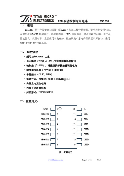
TM1668
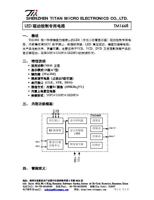
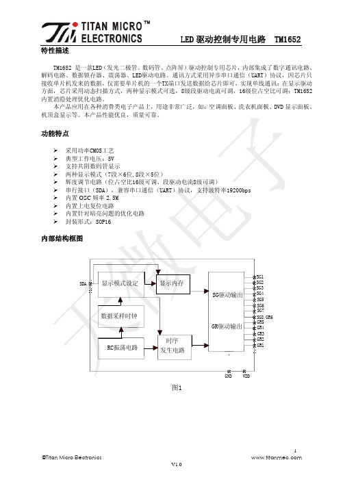
地址:深圳市高新技术产业园中区深圳软件园4号楼401A 室一、 概述TM1668 是一种带键盘扫描接口的LED (发光二极管显示器)驱动控制专用电路,内部集成有MCU 数字接口、数据锁存器、LED 高压驱动、键盘扫描等电路。
本产品性能优良,质量可靠。
主要应用于VCR 、VCD 、DVD 及家庭影院等产品的显示屏驱动。
采用SOP24/SSOP24/SKDIP24的封装形式。
二、 特性说明• 采用功率CMOS 工艺 • 显示模式(10段×7位) • 键扫描(10×2bit )• 辉度调节电路(占空比8级可调) • 串行接口(CLK ,STB ,DI/O )• 振荡方式:内置RC 振荡(450KHz+5%) • 内置上电复位电路• 封装形式:SOP24/SSOP24/SKDIP24三、 内部功能框图:Seg1-10Grid1-7Key1Key2四、 管脚定义:DIOSCLKSTBKEY1KEY2VDD SEG1/KS1 SEG2/KS2 SEG3/KS3 SEG4/KS4 SEG5/KS5 SEG6/KS6GRID1 GRID2 GNDGRID3 GRID4 GRID5 GRID6 GRID7 SEG10/KS10 SEG9/KS9 SEG8/KS8 SEG7/KS7管脚功能定义:符号管脚名称管脚号说明DIO 数据输入/输出 1在时钟上升沿输入串行数据,从低位开始;在时钟下降沿输出串行数据,从低位开始。
输出为N-chopen drainCLK 时钟输入 2 在上升沿读取串行数据,下降沿输出数据STB 片选 3 在上升或下降沿初始化串行接口,随后等待接收指令。
STB为低后的第一个字节作为指令,当处理指令时,当前其它处理被终止。
当STB为高时,CLK被忽略K1~K2 键扫数据输入4~5 输入该脚的数据在显示周期结束后被锁存Seg1/KS1~Seg10/KS10输出(段)7~16 段输出(也用作键扫描)Grid1~Grid2 输出(位) 23~24 位输出Grid3~Grid7 输出(位) 17~21 位输出VDD 逻辑电源 6 5V±10%GND 逻辑地22 接系统地五、 显示寄存器地址和显示模式:地址:深圳市高新技术产业园中区深圳软件园4号楼401A室地址:深圳市高新技术产业园中区深圳软件园4号楼401A 室该寄存器存储通过串行接口从外部器件传送到TM1668 的数据,地址分配如下:六、 键扫描和键扫数据寄存器:键扫矩阵为10×2bit,如下所示:K1 K2SEG1/KS1 SEG2/KS2 SEG3/KS3 SEG4/KS4 SEG5/KS5 SEG6/KS6 SEG7/KS7 SEG8/KS8 SEG9/KS9 SEG10/KS10键扫数据储存地址如下所示,用读指令读取,读从低位开始:K1---K2 K1-----k2Byte0 KS1 KS2 Byte1 KS3 KS4 Byte2 KS5 KS6 Byte3 KS7 KS8 Byte4 KS9 KS10 b0---b1b3----b4读取顺序七、 指令说明:指令用来设置显示模式和LED 驱动器的状态。
导入三合一方案 电源管理大跃进

导入三合一方案电源管理大跃进来源:电子发烧友网作者:孔令双[导读]近两年,随着智能手机、平板电脑、可穿戴设备的持续火爆,电子设备功能的不断完善和增强,电池的尺寸、功耗、充电速率以及安全性等各项功能指标受到巨大挑战,因此,电池管理的地位前所未有的凸显出来。
关键词:快充技术凹凸科技电源管理芯片近两年,随着智能手机、平板电脑、可穿戴设备的持续火爆,电子设备功能的不断完善和增强,电池的尺寸、功耗、充电速率以及安全性等各项功能指标受到巨大挑战,因此,电池管理的地位前所未有的凸显出来。
在“第十一届中国国际电池技术交流会”上,凹凸科技推出世界首颗高集成单节锂电池NVDC1充电器,高精度电池侦测库仑计,高效率OTG升压控制器三合一方案——Killer Whale。
凹凸科技技术市场经理施伟丽表示,此次推出的三合一方案“Killer Whale”主要针对平板电脑、智能手机、移动互联网设备以及其他单电池手持设备应用。
凹凸科技技术市场经理施伟丽表示,“Killer Whale”是全球首颗高集成单节锂电池NVDC1充电器,高精度电池侦测库仑计,高效率OTG升压控制器的三合一方案Killer Whale降压控制器是基于O2Micro的CRC专利架构,具备更快的动态响应,运行频率高达3MHz,可允许使用更小的系统电容,同时集成了4颗开关管以及充电电流侦测电阻,使得应用更简便。
Killer Whale可通过外部的侦测电阻和电池端NTC电阻来检测动态电流,对电池容量进行合理估算,同时基于O2Micro库仑计的专利算法,及OCV侦测功能来初始化和校准修正电池剩余容量,增强电池侦测的准确性,以更提高用户体验。
不仅如此,Killer Whale可实现USB OTG 5V升压输出,内部集成MOSFET和Boost升压控制器可把电池电压提升到5V,使得Killer Whale更适应于手持单节锂电池的应用。
“Killer Whale”具有高集成、高效率、高精度和快瞬态响应的特点,更适应于手持单节锂电池设备的应用智能手机、平板电脑以及互联网其它手持设备注定要往“小”发展,这里的“小”指的是体积小。
TM1913_V1.1
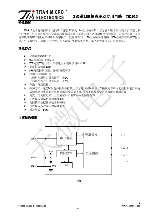
TM1913是具有内控同步功能的三通道LED固定18mA恒流驱动IC,信号输入断开后实现同步固定七彩花样变化,可防止芯片损坏导致的后续级联芯片不工作。
同时适合制作全内控灯条,无需控制器。
芯片内部集成有MCU固化程序和单线数字接口、数据锁存器、LED恒流驱动等电路。
VDD引脚内部集成5V稳压管,外围器件少。
适用于护栏管、点光源等LED装饰类产品。
本产品性能优良,质量可靠。
功能特点图1下降,芯片无法正常工作。
本芯片为单线通讯,采用归一码的方式发送信号。
芯片上电复位后,接收DIN端发来的数据,接收完24bit后,DO端口开始转发DIN端继续发来的数据,为下颗级联芯片提供输入数据。
在转发数据之前,DO端口一直为高电平。
如果DIN端输入Reset复位信号,芯片OUT端口将根据接收到的24bit数据输出相应占空比的PWM波形,且芯片重新等待接收新的数据,在接收完开始的24bit数据后,通过DO端口转发数据,芯片在没有接收到Reset信号前,OUTR、OUTG、OUTB原输出保持不变。
芯片采用自动整形转发技术,信号不会失真衰减。
对于所有级联在一起的芯片,数据传输的周期是一致的。
12、33通道LED恒流驱动专用电路 TM1913图7为防止产品在测试时带电插拔产生的瞬间高压导致芯片信号输入输出引脚损坏,应该在信号输入及输出脚串接100Ω保护电阻。
此外,图中各芯片的104退耦电容不可缺少,且走线到芯片的VDD和GND 脚应尽量短,以达到最佳的退耦效果,稳定芯片工作。
3通道LED恒流驱动专用电路 TM19132、电源配置TM1913可以配置为DC6~24V电压供电,但根据输入电压不同,应配置不同的电源电阻,电阻计算方法:VDD端口电流按10mA计算,VDD串接电阻R=(DC-5.5V)÷10mA(DC为电源电压)。
34,24bit,传输时间为1.25μs×24=30μs。
如果一个系统中共有1000个像素点,一次刷新全部显示的时间为30μs×1000=30ms(忽略Reset信号时间),即一秒钟刷新率为:1÷30ms≈33Hz。
LCD驱动集成电路TM1729规格书V1.0
--
最小值 -
2.5 0.6 1.3 100 100 1.3 0.6 0.6 0.6
TM1729 典型值
-
最大值 0.3 0.3 -
单位
us us us us us ns ns us us us us
8.4. 二线串行数据传输时间波形
SDA
t BUF
t LW
SCL
SDA
t HD:STA
tr
t SDH
SDA SCL
开始条件
停止条件
在利用2线I/F输入命令以及数据时必须形成开始条件和停止条件的固有形态发生。
Slave_Address S0 1111100AC
COMMAND
A C DISPLAY DATA A P
开始条件
ACK 命令或数据判定位
停止条件
本芯片在输入命令或显示数据时,必须按照以下步骤:
©Titan Micro Electronics
V1.0
2
6. 输入/输出等效电路
VDD
VDD
VLCD
GND
GND
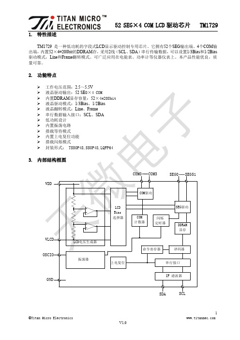
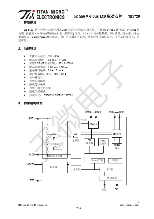
52 SEG×4 COM LCD 驱动芯片 TM1729
VDD TEST1
GND
VDD TEST2
GND
SDA
SCL
VDD
OSCIO
GND
GND
GND
2. 功能特点
工作电压范围:2.5~5.5V 液晶驱动输出:52 SEG×4 COM 内置DDRAM显存容量:52×4=208bit 液晶驱动模式:1/3Bias、1/2Bias 液晶翻转模式:Line、Frame 串行数据输入接口:SCL、SDA 低功耗设计 内置振荡电路 搭载等待模式 内置上电复位功能 搭载闪烁模式 封装形式: TSSOP48,SSOP48,LQFP64
TM2291_V1.1 天微小康
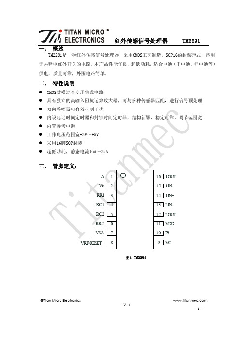
红外传感信号处理器 TM2291©Titan Micro Electronics V1.1定可靠,调节范围12345678109111213141516A Vo RR1RC1RC2RR2VSSVRF/RES ETVCI B VDD 2OUT 2I N-1I N+1I N-1OUT图1 TM2291红外传感信号处理器 TM2291©Titan Micro Electronics V1.1输出延时时间公式:Tx≈40000R 触发封锁时间公式:Ti≈56R 2C 27 一般接0V8 一般接VDD,接“0”时可使定时器复位VC 触发禁止端9 当Vc<V R 时,禁止触发;当Vc>V 触发IB运算放大器偏置电流设置端 10经RB接VSS端,RB取值为1MΩ左右VDD 工作电源正端 11 范围为3~5V2OUT 第二级运算放大器的输出端 122IN- 第二级运算放大器的反相输入端 1IN+ 第一级运算放大器的同相输入端红外传感信号处理器 TM2291©Titan Micro Electronics V1.11OUT第一级运算放大器的输出端16可并联接上2MΩ电阻和10nF电容,再接入第一级运算放大器的反相输入端五、工作原理状态控制器延迟时间定时器Tx封锁时间定时器TiVSSIBVo RR1RC1RR2RC2R1R2RBC1C2图2 TM2291原理框图图2为TM2291红外传感信号处理器的原理框图。
外接元件由使用者根据需要选择。
由图可见TM2291是又运算放大器、电压比较器和状态控制器、延迟定时器、封锁时间定时器及参考电压源等构成的数模混合专用集成电路。
可广泛应用于多种传感器和延时控制器。
红外传感信号处理器 TM2291©Titan Micro Electronics V1.1图4号预处理电路,将信V2OUTVS A VCVoV HV LTxTiTiTxV2OUTVS A VCVoVHVLTiTiTxTx红外传感信号处理器 TM2291©Titan Micro Electronics V1.1图5图5所示为TM2291应用于热释电红外开关的电路原理图。
2021年天微电子产品介绍

发展历程/THE DEVELOPMENT COURSE
2003年成立于深圳国家集成电路设计产业化基地,是深圳首批民营IC设计企业 2004年公司首颗产品TM1628推出,迅速占领市场
2005年公司在LED段位显示驱动占70??市场份额
2006年被认定为深圳市高新技术企业,通过IS09001:2000质量认证 2007年被认定为深圳市第一批自主创新龙头企业
业自动化、LED高端城市亮化、智能家居、物联网以及消费电子等市场。
依托于研发及综合技术能力,天微坚持以客户为中心的战略,理解客户需求。为客户提供全面、 高效的集成方案和服务,公司秉承“严谨创芯、无微不至”的宗旨,打造民族集成电路的产业链,以
自主研发的新技术和高品质产品回馈社会,推动我国民族集成电路产业的发展,把天微建设成为世界
TITAN MICRO°
ELECTRONICS
2021
天微电子产品介绍
公司简介/CoMPANY INTRODUCE
深圳市天微电子股份有限公司成立于2003年,总部位于深圳市南山区高新技术产业园北区紫光信
息港,天微是以集成电路(IC)设计、集成电路封装、产业化营销为特色的综合性企业。天微围绕客
户的需求持续创新,有超过3,000家客户在使用天微的集成电路产品,包括LED/LCD显示驱动、电源管
TM1629A
3线SPI
128
16*8
N管下拉/共阴
8*2
SOP32
TM1629B
3线SPI
112
14*8
N管下拉/共阴
8*1
SOP32
LED面板显示驱动芯片
产品型号
TM1629C TM1629D TM1629 TM1630
tm1651_V1.0 天微小康
无关项, 填0
灰度设置
显示开关设置
八、串行数据传输格式
微处理器的数据通过两线总线接口和 TM1651 通信,在输入数据时当 CLK 是高电平 时,DIO 上的信号必须保持不变;只有 CLK 上的时钟信号为低电平时,DIO 上的信号才 能改变。数据输入的开始条件是 CLK 为高电平时,DIO 由高变低;结束条件是 CLK 为高 时,DIO 由低电平变为高电平。 TM1651 的数据传输带有应答信号 ACK, 当传输数据正确时, 会在第八个时钟的下降 沿,芯片内部会产生一个应答信号 ACK 将 DIO 管脚拉低,在第九个时钟的上升沿释放 DIO 口线。
初始化
发送写显存的数据命令
设置显存地址
传送1Byte数据 NO
送完数据?
发送显示控制命令
发送读按键命令
读按键数据并存储到MCU寄存器
有键按下?
YES
按键处理程序 NO
结束
Page 7 of 16
V1.0
LED 驱动控制专用电路
十 、参考程序
TM1651
/* *版权信息: 深圳天微电子 *文件名: TM1651 *当前版本: 1.0 *单片机型号: AT89S52 *开发环境: Keil uVision3 *晶震频率: 11.0592M *程序功能: 把 TM1651 所有显示寄存器地址全部写满数据 0xff,并开显示,然后再读按键值。 */ #include<reg52.h> #include<intrins.h> //定义端口 sbit clk = P1^2; sbit dio = P1^1; ///======================================= void Delay_us(unsigned int i) //nus 延时 { for(;i>0;i--) _nop_(); } ///====================================== void I2CStart(void) // 1651 开始 { clk = 1; dio = 1; Delay_us(2); dio = 0; } //============================================= void I2Cask(void) //1651 应答 { clk = 0; Delay_us(5); while(dio); clk = 1; Delay_us(2); clk=0; //在第八个时钟下降沿之后延时 5us,开始判断 ACK 信号
3130简明使用手册
注意: z 不要拉扯毛细管 z 使用原包装来储存使用过的毛
细管,其末端分别放在缓冲液槽 和小玻璃瓶中 z 安装毛细管时要戴无粉手套
更换新的胶:
第 9 页 共 32 页
AppliedBiosystems 3130 简明使用手册
z 在DC软件中,选择GA Instruments > ga3130 > instrument name >.
z 若无效,更换毛细管
检测窗口的前表面
3.光谱校正(spectral calibration):
什么是光谱校正?
从下图可以看到,四(或五)色荧光检测系统的本质是检测四(或五)种荧光素在其中 心发射波长处的信号。由于每一种荧光素的发射光谱不是锐线光谱,而是 一种有一定宽度 分布的光谱带。所以一个纯荧光除在它自己光谱的中心波长处能采 集到信号N1外,在其他 荧光信号光谱的中心波长处亦能检测到信号而产生信号重叠。为了校准信号重叠,需知道一 种荧光信号在其他荧光信号处产生的重叠系数。 所以,我们用四(或五)条不同长度的D NA片断分别标记上不同的荧光素来计算这些系数。最后得到一个4x4(或5x5)的数 据矩阵。
样品准备 z 按照试剂盒说明书用
Hi-Di甲酰胺混合校正 标准样品 z 震荡离心 z 95度变性5分钟后立即 冰浴2分钟 z 震荡离心 z 在样品板中加入样品 (96孔板加10ul,384孔 板加5ul) z 用橡胶垫装配样品板, 装配后橡胶垫必须平 整,样品板上的孔与橡 胶垫上的孔要对齐,如 图
准备缓冲液:
z 把5ml 10X缓冲液与45ml MilliQ水混合成1X缓冲液;
z 按下Tray按钮,待自动进样 器停止移动后开门;
天微电子 TM2803 说明书
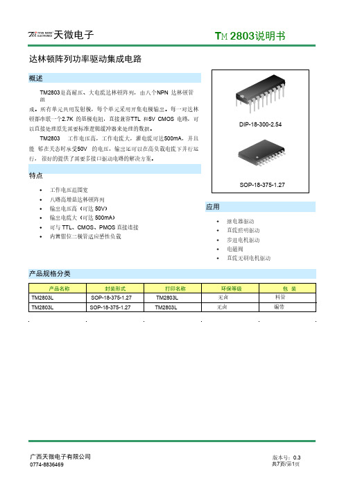
达林顿阵列功率驱动集成电路概述TM2803是高耐压、大电流达林顿阵列,由八个NPN 达林顿管组成。
所有单元共用发射极,每个单元采用开集电极输出。
每一对达林顿都串联一个2.7K 的基极电阻,直接兼容TTL 和5V CMOS 电路,可以直接处理原先需要标准逻辑缓冲器来处理的数据。
TM2803 工作电压高,工作电流大,灌电流可达500mA,并且能够在关态时承受50V 的电压,输出还可以在高负载电流下并行运行,很好的提供了需要多接口驱动电路的解决方案。
特点♦工作电压范围宽♦八路高增益达林顿阵列♦输出电压高(可达50V)♦输出电流大(可达500mA)♦可与TTL、CMOS、PMOS直接连接♦内置钳位二极管适应感性负载应用♦继电器驱动♦直流照明驱动♦步进电机驱动♦电磁阀♦直流无刷电机驱动产品规格分类电路框图GNDTM2803 管脚说明表极限参数电气特性参数(除非特别指定Ta=25°C)注:1、极限值是指超出该范围,器件有可能被损坏,并非器件的正常工作条件范围。
电参数表提供了器件的工作条件范围;2、除特别指明外,所有条件适用于达林顿阵列;3、通常条件下,每路输出在 70°C、VCE (Sat)= 1.6V 下脉冲宽度为 20ms 的持续工作电流为350mA。
典型特性曲线集电极峰值电流 - m ADUTY CYCLE - %图 4. 集电极峰值电流vs.几路同时导通1004006080100集电极电流 - m A饱和压降 - V图1. 集电极电流vs. 饱和压降2000.580004006001.01.52003002040集电极电流 - m A输入电流 - uA图2. 集电极电流vs. 输入电流1002004000200300400600输入电流 - m A输入电压 - V 图3. 输入电流vs. 输入电压0.542.501.02.02691.53578内部等效线路图INOUTCOMMON测试线路图OPEN+50VC图2C图7图3COPEN+50V 图8OPENF封装外形图声明:∙天微保留说明书的更改权,恕不另行通知!客户在下单前应获取最新版本资料,并验证相关信息是否完整和最新。
TM1722_V1.1 天微电子

LCD驱动控制专用电路 TM1722一、 概述TM1722是一种LCD驱动控制专用电路,内部集成有MCU 数字接口、数据锁存器、LCD驱动、幻彩背光驱动等电路。
本产品性能优良,质量可靠,无须更改解码板底层指令,与天微现有LED驱动IC的指令集完全兼容。
同时支持PWM背光驱动;主要应用于VCR、VCD、DVD 及家庭影院等产品的显示屏驱动。
二、 特性说明Ø采用低功耗CMOS工艺Ø最大15X4点LCD驱动Ø3路LED驱动,具有64级PWM,可用于LCD幻彩背光驱动;Ø1/2或1/3LCD驱动偏压可选ØLCD工作电压可调Ø串行接口(CLK,STB,DIO)Ø振荡方式:内置RC振荡,典型振荡频率为128KHZØ封装形式:SOP24三、 管脚定义- 1 - ©Titan Micro Electronics LCD驱动控制专用电路 TM1722四、管脚功能定义:- 2 - ©Titan Micro Electronics LCD驱动控制专用电路 TM1722五、 显示寄存器该寄存器存储通过串行接口从外部器件传送到TM1722的数据,地址从00H-0FH共16字节单元,实际的地址有02H、03H、06H、07H、0AH、0BH、0EH、0FH共8字节单元,分别与芯片SGE和COM 管脚所接的LCD灯对应,没有的SEG引脚相对应的地址单元写0。
分配如下图:写LCD显示数据的时候,按照从显示地址从低位到高位,从数据字节的低位到高位操作。
上电后所有寄存器初始状态为0- 3 - ©Titan Micro Electronics LCD驱动控制专用电路 TM1722七、 指令说明指令用来设置显示模式和LCD 驱动器的状态。
在STB下降沿后由DIO输入的第一个字节作为一条指令。
经过译码,取最高B7、B6两位比特位以区别不同的指令。
微片微电子MSC017SMA120S 1200V 17mΩ SiC MOSFET 产品概述说明书

Product OverviewThe silicon carbide(SiC)power MOSFET product line from Microsemi increases the performance over siliconMOSFET and silicon IGBT solutions while lowering the total cost of ownership for high-voltage applications.The MSC017SMA120S device is a1200V,17mΩSiC MOSFET in a TO-268(D3PAK)package.FeaturesThe following are key features of the MSC017SMA120S device:•Low capacitances and low gate charge•Fast switching speed due to low internal gate resistance(ESR)•Stable operation at high junction temperature,T J(max)=175°C•Fast and reliable body diode•Superior avalanche ruggedness•RoHS compliantBenefitsThe following are benefits of the MSC017SMA120S device:•High efficiency to enable lighter,more compact system•Simple to drive and easy to parallel•Improved thermal capabilities and lower switching losses•Eliminates the need for external freewheeling diode•Lower system cost of ownershipApplicationsThe MSC017SMA120S device is designed for the following applications:•PV inverter,converter,and industrial motor drives•Smart grid transmission and distribution•Induction heating and welding•H/EV powertrain and EV charger•Power supply and distributionThis section shows the specifications of the MSC017SMA120S device.Absolute Maximum RatingsThe following table shows the absolute maximum ratings of the MSC017SMA120S device.Table1•Absolute Maximum RatingsSymbolParameterRatingsUnitV DSSDrain source voltageV1200Continuous drain current at T C=25°CI DA100Continuous drain current at T C=100°C71I DM280Pulsed drain current1V GSGate-source voltage23to–10VTotal power dissipation at T C=25°CP D357WLinear derating factor3.33W/°CNote:1.Repetitive rating:pulse width and case temperature limited by maximum junction temperature. The following table shows the thermal and mechanical characteristics of the MSC017SMA120S device. Table2•Thermal and Mechanical CharacteristicsCharacteristicMinSymbolTypMaxUnitRθJCJunction-to-case thermal resistance0.280.42°C/W Operating junction temperatureT J–55175°CT STG–55150Storage temperatureT LSoldering temperature for10seconds(1.6mm from case)300WtPackage weight0.14ozg4.0Electrical PerformanceThe following table shows the static characteristics of the MSC017SMA120S device.T J =25°C unless otherwise specified.Table 3•Static CharacteristicsUnit MaxTypMin Test Conditions CharacteristicSymbol V 1200V GS =0V,I D =100µA Drain-source breakdown voltage V (BR)DSS mΩ2217.6V GS =20V,I D =40A Drain-source on resistance 1R DS(on)V 2.71.9V GS =V DS,I D =4.5mA Gate-source threshold voltage V GS(th)mV/°C –4.6V GS =V DS ,I D =4.5mA Threshold voltage coefficient ΔV GS(th)/ΔT J µA100V DS ,=1200V,V GS =0V Zero gate voltage drain currentI DSS500V DS =1200V,V GS =0V T J =125°CnA±100V GS =20V/–10VGate-source leakage currentI GSSNote:1.Pulse test:pulse width <380µs,duty cycle <2%.The following table shows the dynamic characteristics of the MSC017SMA120S device.T J =25°C unless otherwise specified.Table 4•Dynamic CharacteristicsUnit MaxTyp MinTest Conditions Characteristic Symbol pF5280V GS =0V,V DD =1000V V AC =25mV,ƒ=1MHzInput capacitanceC iss 12Reverse transfer capacitance C rss 265Output capacitance C oss nC249V GS =–5V/20V,V DD =800V I D =40ATotal gate charge Q g 63Gate-source charge Q gs 32Gate-drain charge Q gd ns52V DD =800V,V GS =–5V/20V,I D =50A,R g(ext)=4.0Ω,Turn-on delay time t d(on)21Voltage fall time t f Freewheeling diode =MSC017SMA120S (V GS =–5V)49Turn-off delay timet d(off)UnitMax Typ Min Test Conditions Characteristic Symbol 16Voltage rise time t r µJ1677Turn-on switching energy E on 395Turn-off switching energy E off ns49V DD =800V,V GS =–5V/20V,I D =50A,R g(ext)=4.0ΩTurn-on delay time t d(on)19Voltage fall time t f Freewheeling diode =MSC050SDA120B49Turn-off delay time t d(off)14Voltage rise time t r µJ1329Turn-on switching energy E on 429Turn-off switching energy E off Ω0.71f =1MHz,25mV,drain short Equivalent series resistance ESR µs 3V DS =960V,V GS =20V Short circuit withstand time SCWT mJ3500V DS =150V,I D =30AAvalanche energy,single pulseE ASThe following table shows the body diode characteristics of the MSC017SMA120S device.T J =25°C unless otherwise specified.Table 5•Body Diode CharacteristicsUnit MaxTyp MinTest Conditions Characteristic Symbol V 3.5I SD =40A,V GS =0V Diode forward voltageV SDV 3.9I SD =40A,V GS =–5Vns40I SD =50A,V GS =–5V,Drive Rg =4ΩReverse recovery time t rr nC 490Reverse recovery charge Q rr V DD =800V,dl/dt =–2500A/µsA22Reverse recovery currentI RRMTypical Performance CurvesThis section shows the typical performance curves of the MSC017SMA120S device.Figure2•Drain Current vs.V DS Figure1•Drain Current vs.V DSFigure4•Drain Current vs.V DS Figure3•Drain Current vs.V DSFigure5•RDS(on)vs.Junction TemperatureFigure6•Gate Charge CharacteristicsFigure8•I D vs.V DS3rd Quadrant Conduction Figure7•Capacitance vs.Drain-to-Source VoltageFigure10•Switching Energy Eon vs.V DS&I D Figure9•I D vs.V DS3rd Quadrant ConductionFigure11•Switching Energy Eoff vs.V DS&I DFigure12•Switching Energy vs.R gFigure13•Switching Energy vs.TemperatureFigure14•Switching Energy Eon vs.V DS&I DFigure16•Switching Energy vs.R gFigure15•Switching Energy Eoff vs.V DS&I DFigure17•Threshold Voltage vs.Junction Temp.Figure18•Forward Safe Operating AreaFigure19•Maximum Transient Thermal ImpedanceThis section shows the package specification of the MSC017SMA120S device.Package Outline DrawingThe following figure illustrates the TO-268package outline of the MSC017SMA120S device.Figure20•Package Outline DrawingThe following table shows the TO-268dimensions and should be used in conjunction with the package outline drawing.Table6•TO-268DimensionsSymbolMin(mm)Min(in.)Max(mm)Max(in.)4.90A5.100.1930.201B15.850.63816.200.624C18.7019.100.7520.7361.00D1.250.0490.03913.80E14.000.5510.543F13.300.5240.53513.60Min(mm)Min(in.)Max(mm)G2.700.1060.1142.90H1.151.450.0570.045I1.950.0772.210.087J0.940.0550.0371.40K2.400.1060.0942.70L0.400.0240.600.016M1.450.0630.0571.60N0.000.0070.180.00012.40O12.700.4880.500P5.45BSC(nom.)0.215BSC(nom.)GateTerminal1DrainTerminal2SourceTerminal3DrainTerminal4Microsemi's product warranty is set forth in Microsemi's Sales Order Terms and rmation contained in this publication is provided for the sole purpose of designing with and using Microsemi rmation regarding device applications and the like is provided only for your convenience and may be superseded by updates.Buyer shall not rely on any data and performance specifications or parameters provided by Microsemi.It is your responsibility to ensure that your application meets with your specifications.THIS INFORMATION IS PROVIDED "AS IS."MICROSEMI MAKES NO REPRESENTATIONS OR WARRANTIES OF ANY KIND WHETHER EXPRESS OR IMPLIED,WRITTEN OR ORAL,STATUTORY OR OTHERWISE,RELATED TO THE INFORMATION,INCLUDING BUT NOT LIMITED TO ITS CONDITION,QUALITY ,PERFORMANCE,NON-INFRINGEMENT,MERCHANTABILITY OR FITNESS FOR A PARTICULAR PURPOSE.IN NO EVENT WILL MICROSEMI BE LIABLE FOR ANY INDIRECT,SPECIAL,PUNITIVE,INCIDENTAL OR CONSEQUENTIAL LOSS,DAMAGE,COST OR EXPENSE WHATSOEVER RELATED TO THIS INFORMATION OR ITS USE,HOWEVER CAUSED,EVEN IF MICROSEMI HAS BEEN ADVISED OF THE POSSIBILITY OR THE DAMAGES ARE FORESEEABLE.TO THE FULLEST EXTENT ALLOWED BY LAW,MICROSEMI’S TOTAL LIABILITY ON ALL CLAIMS IN RELATED TO THIS INFORMATION OR ITS USE WILL NOT EXCEED THE AMOUNT OF FEES,IF ANY ,YOU PAID DIRECTLY TO MICROSEMI FOR THIS e of Microsemi devices in life support,mission-critical equipment or applications,and/or safety applications is entirely at the buyer’s risk,and the buyer agrees to defend and indemnify Microsemi from any and all damages,claims,suits,or expenses resulting from such use.No licenses are conveyed,implicitly or otherwise,under any Microsemi intellectual property rights unless otherwisestated.Microsemi2355W.Chandler Blvd.Chandler,AZ 85224USAWithin the USA:+1(480)792-7200Fax:+1(480)792-7277 ©2020Microsemi andits corporate affiliates.All rights reserved.Microsemi and the Microsemi logo aretrademarks of Microsemi Corporation and itscorporate affiliates.All other trademarks andservice marks are the property of theirrespective owners.Microsemi Corporation,a subsidiary of Microchip Technology Inc.(Nasdaq:MCHP),and its corporate affiliates are leading providers of smart,connected and secure embedded control solutions.Their easy-to-use development tools and comprehensive product portfolio enable customers to create optimal designs which reduce risk while lowering total system cost and time to market.These solutions serve more than 120,000customers across the industrial,automotive,consumer,aerospace and defense,communications and computing markets.Headquartered in Chandler,Arizona,the company offers outstanding technical support along with dependable delivery and quality.Learn more at .050-7781|October 2020|Preliminary11050-7781MSC017SMA120S Datasheet RevisionA Legal。
DW03_V1.0

概述DW03是一款高精度的单节可充电锂电池保护芯片,芯片内部集成了功率管以及高精度的过电压充电、过电压放电、过电流充电和过电流放电等保护电路。
同时,DW03具有短路保护、过温保护、充电器检测和0V电池充电允许等功能。
正常工作状态下,DW03的VDD 脚电压保持在过电压充电保护阈值和过电压放电保护阈值之间,同时DW03的充/放电流在过电流充电保护阈值和过电流放电保护阈值之间,此时DW03内置的功率管导通,既可以使用充电器对电池充电,也可以通过负载对电池放电。
当充/放电保护条件发生时,并持续相应的延时后,DW03内置的功率管开始关闭,此时充/放电过程停止。
DW03对每种保护状态都有相应的恢复条件,当恢复条件满足,并持续相应的延时后,DW03内置的功率管再次导通,芯片重新进入正常工作状态。
DW03采用体积超小的SOT23-3L封装,外围应用电路精简,只需要一个电容和一个电阻。
这非常适合对空间限制要求非常严格的可充电锂电池组的应用。
特点∙集成功率管:R ON=55mΩ∙过电压充电/放电保护∙过电流放电保护∙异常充电/过电流充电保护∙0V电池充电允许∙充电器检测功能∙延时时间内部设定∙负载短路保护∙充电器反接保护∙过温保护∙超低静态电流:工作状态:典型值2.5uA低功耗状态:典型值1.5uA ∙极少的外围元器件∙采用SOT23-3L封装应用∙单节锂离子电池组∙单节锂聚合物电池组典型应用电路管脚SOT23-3L管脚描述极限参数(注1)注1: 最大极限值是指超出该工作范围芯片可能会损坏。
推荐工作范围是指在该范围内芯片工作正常,但不完全保证满足个别性能指标。
电气参数定义了器件在工作范围内并且在保证特定性能指标的测试条件下的直流和交流电气参数规范。
对于未给定的上下限参数,该规范不予保证其精度,但其典型值合理反映了器件性能。
注2:环境温度升高最大功耗会减小,这是由T JMAX,ѲJA和环境温度T A所决定的。
最大允许功耗为P DMAX=(T JMAX-T A)/ ѲJA或是极限参数范围给出的数值中比较低的那个值。
TM1652_V1.0天微电子
SG驱动强度 8/8,SG1~SG8端口 为高电平时加压3V
测试
SG 驱动强度 8/8,SG1~SG8 端口 为高电平时加压 2V
测试
GR1~GR6 端口为低 电平时加压 0.3V
测试
VDD=5V,其它脚悬 空
最小值
20
20 80 —
TM1652 典型值
25
30 140 —
最大值
30
40 — ±1
单位
特性描述
LED 驱动控制专用电路 TM1652
TM1652 是一款LED(发光二极管、数码管、点阵屏)驱动控制专用芯片,内部集成了数字通讯电路、 解码电路、数据锁存器、震荡器、LED驱动电路。通讯方式采用异步串口通信(UART)协议,因芯片只 接收单片机发来的数据,仅需要单片机的一个TX端口发送数据给芯片即可,实现单线通讯;在显示驱动 方面,芯片采用动态扫描方式,两种显示模式可选,8级段驱动电流可调,16级位占空比可调;TM1652 内置消隐处理优化电路。
输入输出等效电路
GRx
SDA
SGx
图3
©Titan Micro Electronics
V1.0
2
LED 驱动控制专用电路 TM1652
集成电路系静电敏感器件,在干燥季节或者干燥环境使用容易产生大量静电,静电放电可能会损坏集成电路, 天微电子建议采取一切适当的集成电路预防处理措施,不正当的操作 焊接,可能会造成 ESD 损坏或者性能下降,芯片无法正常工作。
V
VDD=5V
—
0.35
—
V
无负载,显示关
—
—
5
mA
开关特性
在-20℃~+85℃下测试,除非另有说明 VDD=5V, GND=0V
TM1729_V1.1
SDA SCL
开始条件
停止条件
在利用2线I/F输入命令以及数据时必须形成开始条件和停止条件的固有形态发生。
Slave_Address S 0 1 1 1 1 10 0 A C
COMMAND
A C DISPLAY DATA A P
开始条件
ACK 命令 或数据判 定位
停止条件
本芯片在输入命令或显示数据时,必须按照以下步骤:
输出“L”信号。然后第9个信号下降时输出停止。
但是,输出时为了NMOS开路的形式,H电平不输出。
在不需要ACK信号时,从SCL信号的第8个信号下降到第9个信号的下降为止请输入“L”。
开始条件
停止条件
SDA
SCL
1-7 8 9
1-7 8 9
1-7 8 9
ACK
ACK
ACK
9.3. Command的传送方法 开始条件生成后,输入Slave Address(0111 1100)。输入Slave Address后,必须输入1byte的命令。
--
开始条件建立时间 tSU:STA
--
停止条件建立时间 tSU:STO
--
最小值 -
2.5 0.6 1.3 100 100 1.3 0.6 0.6 0.6
TM1729 典型值
-
最大值 0.3 0.3 -
单位
us us us us us ns ns us us us us
8.4. 二线串行数据传输时间波形
命令的MSB位是判断下一组数据是命令还是显示数据(即MSB位是Command或Display Data的判定位)。 Command或Display Data的判定位只有为“1”,才有可能输入后续的命令; Command或Display Data的判定位只有为“0”,才有可能输入后续的显示数据。
LME49740MANOPB,LME49740NANOPB,LME49740MAXNOPB,LME49740MABD,LME49740NABD, 规格书,Datasheet 资料

LME49740LME49740 Quad High Performance, High Fidelity Audio Operational AmplifierLiterature Number: SNAS377A芯天下--/February 8, 2008LME49740Quad High Performance, High Fidelity Audio Operational AmplifierGeneral DescriptionThe LME49740 is part of the ultra-low distortion, low noise,high slew rate operational amplifier series optimized and fully specified for high performance, high fidelity bining advanced leading-edge process technology with state-of-the-art circuit design, the LME49740 audio opera-tional amplifiers deliver superior audio signal amplification for outstanding audio performance. The LME49740 combines extremely low voltage noise density (2.7nV/√HZ) with van-ishingly low TH D+N (0.00003%) to easily satisfy the most demanding audio applications. To ensure that the most chal-lenging loads are driven without compromise, the LME49740has a high slew rate of ±20V/μs and an output current capa-bility of ±26mA. Further, dynamic range is maximized by an output stage that drives 2k Ω loads to within 1V of either power supply voltage and to within 1.4V when driving 600Ω loads.The LME49740's outstanding CMRR(120dB), PSRR(120dB),and V OS (0.1mV) give the amplifier excellent operational am-plifier DC performance.The LME49740 has a wide supply range of ±2.5V to ±17V.Over this supply range the LME49740’s input circuitry main-tains excellent common-mode and power supply rejection, as well as maintaining its low input bias current. The LME49740is unity gain stable. The Audio Operational Amplifier achieves outstanding AC performance while driving complex loads with values as high as 100pF.The LME49740 is available in 14–lead narrow body SOIC and 14–lead plastic DIP. Demonstration boards are available for each package.Key Specifications■ Power Supply Voltage Range ±2.5V to ±17V■ THD+N (A V = 1, V OUT = 3V RMS , f IN = 1kHz)R L = 2k Ω0.00003% (typ) R L = 600Ω0.00003% (typ)■ Input Noise Density 2.7nV/√Hz (typ)■ Slew Rate±20V/μs (typ)■ Gain Bandwidth Product 55MHz (typ)■ Open Loop Gain (R L = 600Ω)140dB (typ)■ Input Bias Current 10nA (typ)■ Input Offset Voltage 0.1mV (typ)■ DC Gain Linearity Error0.000009%Features■Easily drives 600Ω loads■Optimized for superior audio signal fidelity ■Output short circuit protection■PSRR and CMRR exceed 120dB (typ)■SOIC and DIP packagesApplications■Ultra high quality audio amplification ■High fidelity preamplifiers ■High fidelity multimedia■State of the art phono pre amps■High performance professional audio■High fidelity equalization and crossover networks ■High performance line drivers ■High performance line receivers ■High fidelity active filters© 2008 National Semiconductor Corporation LME49740 Quad High Performance, High Fidelity Audio Operational AmplifierTypical Application20210502FIGURE 1. Passively Equalized RIAA Phono PreamplifierConnection Diagram20210501Order Number LME49740MA See NS Package Number — M14A Order Number LME49740NA See NS Package Number — N14A 2L M E 49740Absolute Maximum Ratings (Notes 1, 2)If Military/Aerospace specified devices are required,please contact the National Semiconductor Sales Office/Distributors for availability and specifications.Power Supply Voltage (V S = V + - V -)36VStorage Temperature −65°C to 150°CInput Voltage(V-) - 0.7V to (V+) + 0.7VOutput Short Circuit (Note 3)Continuous Power DissipationInternally LimitedESD Susceptibility (Note 4)2000V ESD Susceptibility (Note 5)200V Junction Temperature 150°CThermal Resistance θJA (MA)107°C/W θJA (NA)74°C/WTemperature RangeT MIN ≤ T A ≤ T MAX –40°C ≤ T A ≤ 85°C Supply Voltage Range±2.5V ≤ V S ≤ ± 17VElectrical Characteristics(Notes 1, 2)The following specifications apply for V S = ±15V, R L = 2k Ω, f IN = 1kHz,and T A = 25C, unless otherwise specified.SymbolParameterConditionsLME49740Units (Limits)Typical Limit (Note 6)(Notes 7, 8)THD+NTotal Harmonic Distortion + NoiseA V = 1, V OUT = 3V RMSR L = 2k Ω R L = 600Ω0.000030.000030.00009% (max)% (max)IMD Intermodulation Distortion A V = 1, V OUT = 3V RMSTwo-tone, 60Hz & 7kHz 4:10.00005 % (max)GBWP Gain Bandwidth Product 5545MHz (min)SR Slew Rate±20±15V/μs (min)FPBWFull Power BandwidthV OUT = 1V P-P , –3dBreferenced to output magnitude at f = 1kHz10MHzt sSettling timeA V = 1, 10V step, C L = 100pF 0.1% error range 1.2μs e nEquivalent Input Noise Voltagef BW = 20Hz to 20kHz 0.340.65μV RMSEquivalent Input Noise Density f = 1kHz f = 10Hz 2.76.4 4.7 nV /√Hz nV /√Hz i n Current Noise Density f = 1kHz f = 10Hz 1.63.1 pA /√Hz pA /√HzV OSOffset Voltage±0.1±0.7mV (max)ΔV OS /ΔTemp Average Input Offset Voltage Drift vsTemperature40°C ≤ T A ≤ 85°C0.2 μV/°C PSRR Average Input Offset Voltage Shift vsPower Supply Voltage ΔV S = 20V (Note 9)120110dB (min)ISO CH-CH Channel-to-Channel Isolation f IN = 1kHz f IN = 20kHz 118112 dB dB I BInput Bias Current V CM = 0V1072nA (max)ΔI OS /ΔTemp Input Bias Current Drift vs Temperature –40°C ≤ T A ≤ 85°C 0.1 nA/°C I OS Input Offset CurrentV CM = 0V1165nA (max)V IN-CM Common-Mode Input Voltage Range +14.1–13.9(V+)–2.0(V-)+2.0V (min)V (min)CMRR Common-Mode Rejection –10V<V CM <10V 120110dB (min)Z INDifferential Input Impedance30 k ΩCommon Mode Input Impedance –10V<V CM <10V1000 M ΩA VOLOpen Loop Voltage Gain–10V<V OUT <10V, R L = 600Ω140 dB (min)–10V<V OUT <10V, R L = 2k Ω140 dB (min)–10V<V OUT <10V, R L = 10k Ω140125dB (min)3LME49740SymbolParameterConditionsLME49740Units (Limits)Typical Limit (Note 6)(Notes 7, 8)V OUTMAX Maximum Output Voltage Swing R L = 600Ω±13.6±12.5V (min)R L = 2k Ω±14.0 V (min)R L = 10k Ω±14.1 V (min)I OUT Output Current R L = 600Ω, V S = ±17V ±26±23mA (min)I OUT-CC Short Circuit Current+30–38 mA mA R OUT Output Impedancef IN = 10kHz Closed-Loop Open-Loop 0.0113ΩΩC LOAD Capacitive Load Drive Overshoot 100pF 16 %I STotal Quiescent CurrentI OUT = 0mA18.520mA (max)Note 1:Absolute Maximum Ratings indicate limits beyond which damage to the device may occur.Note 2:Operating Ratings indicate conditions for which the device is functional, but do not guarantee specific performance limits. For guaranteed specifications and test conditions, see the Electrical Characteristics. The guaranteed specifications apply only for the test conditions listed. Some performance characteristics may degrade when the device is not operated under the listed test conditions.Note 3:Amplifier output connected to GND, any number of amplifiers within a package.Note 4:Human body model, 100pF discharged through a 1.5k Ω resistor.Note 5:Machine Model ESD test is covered by specification EIAJ IC-121-1981. A 200pF cap is charged to the specified voltage and then discharged directly into the IC with no external series resistor (resistance of discharge path must be under 50Ω).Note 6:Typical specifications are specified at +25ºC and represent the most likely parametric norm.Note 7:Tested limits are guaranteed to National's AOQL (Average Outgoing Quality Level).Note 8:Datasheet min/max specification limits are guaranteed by design, test, or statistical analysis.Note 9:PSRR is measured as follows: V OS is measured at two supply voltages, ±5V and ±15V. PSRR = |20log(ΔV OS /ΔV S )|. 4L M E 49740Typical Performance CharacteristicsTHD+N vs Output Voltage V CC = 15V, V EE = –15V, R L = 2k Ω20210515THD+N vs Output Voltage V CC = 17V, V EE = –17V, R L = 2k Ω20210516THD+N vs FrequencyV CC = 15V, V EE = –15V, R L = 2k Ω, V OUT = 3V RMS 20210511THD+N vs FrequencyV CC = 17V, V EE = –17V, R L = 2k Ω, V OUT = 3V RMS20210513THD+N vs FrequencyV CC = 15V, V EE = –15V, R L = 600Ω, V OUT = 3V RMS 20210512THD+N vs FrequencyV CC = 17V, V EE = –17V, R L = 600Ω, V OUT = 3V RMS20210514LME49740IMD vs Output VoltageV CC = 15V, V EE = –15V, R L = 2k Ω20210553IMD vs Output VoltageV CC = 17V, V EE = –17V, R L = 2k Ω20210554PSRR+ vs Frequency V CC = 15V, V EE = –15V,R L = 2k Ω, V RIPPLE = 200mVpp20210559PSRR- vs FrequencyV CC = 15V, V EE = –15V, R L = 2k ΩR L = 2k Ω, V RIPPLE = 200mVpp20210560CMRR vs FrequencyV CC = 15V, V EE = –15V, R L = 2k Ω20210552Crosstalk vs Frequency V CC = 15V, V EE = –15V, R L = 2k Ω20210519 6L M E 49740Output Voltage vs Supply VoltageRL= 2kΩ, THD+N = 1%20210518Output Voltage vs Load ResistanceTHD+N = 1%20210517Supply Current vs Supply VoltageRL= 2kΩ, THD+N = 1%20210507Full Power Bandwidth vs Frequency20210520Gain Phase vs Frequency20210551Voltage Noise Density vs Frequency20210557LME49740Small-Signal Transient ResponseA V = 1, C L = 100pF 20210556Large-Signal Transient ResponseA V = 1, C L = 100pF20210555 8L M E 49740Application InformationDISTORTION MEASUREMENTSThe vanishingly low residual distortion produced by LME49740 is below the capabilities of all commercially avail-able equipment. This makes distortion measurements just slightly more difficult than simply connecting a distortion me-ter to the amplifier’s inputs and outputs. The solution, how-ever, is quite simple: an additional resistor. Adding this resistor extends the resolution of the distortion measurement equipment.The LME49740’s low residual distortion is an input referred internal error. As shown in Figure 2, adding the 10Ω resistor connected between the amplifier’s inverting and non-inverting inputs changes the amplifier’s noise gain. The result is that the error signal (distortion) is amplified by a factor of 101. Al-though the amplifier’s closed-loop gain is unaltered, the feed-back available to correct distortion errors is reduced by 101, which means that measurement resolution increases by 101. To ensure minimum effects on distortion measurements, keep the value of R1 low as shown in Figure 2.This technique is verified by duplicating the measurements with high closed loop gain and/or making the measurements at high frequencies. Doing so produces distortion compo-nents that are within the measurement equipment’s capabili-ties. This datasheet’s THD+N and IMD values were generat-ed using the above described circuit connected to an Audio Precision System Two Cascade.20210562FIGURE 2. THD+N and IMD Distortion Test Circuit LME49740Application HintsThe LME49740 is a high speed op amp with excellent phase margin and stability. Capacitive loads up to 100pF will cause little change in the phase characteristics of the amplifiers and are therefore allowable.Capacitive loads greater than 100pF must be isolated from the output. The most straightforward way to do this is to put a resistor in series with the output. This resistor will also pre-vent excess power dissipation if the output is accidentally shorted.Noise Measurement Circuit20210527Complete shielding is required to prevent induced pick up from external sources. Always check with oscilloscope for power line noise.Total Gain: 115 dB at f = 1 kHzInput Referred Noise Voltage: e n = V O /560,000 (V)RIAA Preamp Voltage Gain,RIAA Deviation vs Frequency V IN = 10mV, A V = 35.0dB, f = 1kHz20210528Flat Amp Voltage Gain vs Frequency V O = 0dB, A V = 80.0dB, f = 1kHz20210529L M E 49740Typical ApplicationsNAB Preamp20210530A V = 34.5F = 1 kHz E n = 0.38 μV A WeightedNAB Preamp Voltage Gain vs FrequencyV IN = 10mV, A V = 34.5dB, f = 1kHz20210531Balanced to Single Ended Converter 20210532V O = V1–V2Adder/Subtracter20210533V O = V1 + V2 − V3 − V4Sine Wave Oscillator20210534LME49740Second Order High Pass Filter(Butterworth)20210535Illustration is f= 1 kHzSecond Order Low Pass Filter(Butterworth)20210536Illustration is f= 1 kHzState Variable Filter20210537LME4974AC/DC Converter202105382 Channel Panning Circuit (Pan Pot)20210539Line Driver20210540Tone Control20210541LME4974020210542RIAA Preamp20210503A v = 35 dB E n = 0.33 μV S/N = 90 dB f = 1 kHz A WeightedA Weighted, V IN = 10 mV @f = 1 kHzL M E 49740Balanced Input Mic Amp20210543Illustration is:V0 = 101(V2 − V1)LME4974010 Band Graphic Equalizer20210544fo (Hz)C 1C 2R 1R 2320.12μF 4.7μF 75k Ω500Ω640.056μF 3.3μF 68k Ω510Ω1250.033μF 1.5μF 62k Ω510Ω2500.015μF 0.82μF 68k Ω470Ω5008200pF 0.39μF 62k Ω470Ω1k 3900pF 0.22μF 68k Ω470Ω2k 2000pF 0.1μF 68k Ω470Ω4k 1100pF 0.056μF 62k Ω470Ω8k 510pF 0.022μF 68k Ω510Ω16k330pF0.012μF51k Ω510ΩNote 10:At volume of change = ±12 dB Q = 1.7 Reference: “AUDIO/RADIO HANDBOOK”, National Semiconductor, 1980, Page 2–61L M E 49740Revision HistoryRev Date Description1.002/28/07Initial WEB release.1.0102/08/08Fixed the captions on the LME4970MA package (from Dual-In-Line to Molded Package (SO).LME49740Physical Dimensions inches (millimeters) unless otherwise notedMolded Package (SO)Order Number LME49740MA NS Package Number M14ADual-In-Line Package Order Number LME49740NA NS Package Number N14AL M E 49740LME49740NotesL M E 49740 Q u a d H i g h P e r f o r m a n c e , H i g h F i d e l i t y A u d i o O p e r a t i o n a l A m p l i f i e rFor more National Semiconductor product information and proven design tools, visit the following Web sites at:ProductsDesign SupportAmplifiers /amplifiers WEBENCH /webench Audio/audio Analog University /AU Clock Conditioners /timing App Notes /appnotes Data Converters /adc Distributors /contacts Displays /displays Green Compliance /quality/green Ethernet /ethernet Packaging/packaging Interface /interface Quality and Reliability /quality LVDS/lvds Reference Designs /refdesigns Power Management /power Feedback /feedback Switching Regulators /switchers LDOs /ldo LED Lighting /led PowerWise/powerwise Serial Digital Interface (SDI)/sdiTemperature Sensors /tempsensors Wireless (PLL/VCO)/wirelessTHE CONTENTS OF THIS DOCUMENT ARE PROVIDED IN CONNECTION WITH NATIONAL SEMICONDUCTOR CORPORATION (“NATIONAL”) PRODUCTS. NATIONAL MAKES NO REPRESENTATIONS OR WARRANTIES WITH RESPECT TO THE ACCURACY OR COMPLETENESS OF TH E CONTENTS OF TH IS PUBLICATION AND RESERVES TH E RIGH T TO MAKE CH ANGES TO SPECIFICATIONS AND PRODUCT DESCRIPTIONS AT ANY TIME WITH OUT NOTICE. NO LICENSE, WH ETH ER EXPRESS,IMPLIED, ARISING BY ESTOPPEL OR OTH ERWISE, TO ANY INTELLECTUAL PROPERTY RIGH TS IS GRANTED BY TH IS DOCUMENT.TESTING AND OTH ER QUALITY CONTROLS ARE USED TO TH E EXTENT NATIONAL DEEMS NECESSARY TO SUPPORT NATIONAL’S PRODUCT WARRANTY. EXCEPT WH ERE MANDATED BY GOVERNMENT REQUIREMENTS, TESTING OF ALL PARAMETERS OF EACH PRODUCT IS NOT NECESSARILY PERFORMED. NATIONAL ASSUMES NO LIABILITY FOR APPLICATIONS ASSISTANCE OR BUYER PRODUCT DESIGN. BUYERS ARE RESPONSIBLE FOR TH EIR PRODUCTS AND APPLICATIONS USING NATIONAL COMPONENTS. PRIOR TO USING OR DISTRIBUTING ANY PRODUCTS TH AT INCLUDE NATIONAL COMPONENTS, BUYERS SHOULD PROVIDE ADEQUATE DESIGN, TESTING AND OPERATING SAFEGUARDS.EXCEPT AS PROVIDED IN NATIONAL’S TERMS AND CONDITIONS OF SALE FOR SUCH PRODUCTS, NATIONAL ASSUMES NO LIABILITY WH ATSOEVER, AND NATIONAL DISCLAIMS ANY EXPRESS OR IMPLIED WARRANTY RELATING TO TH E SALE AND/OR USE OF NATIONAL PRODUCTS INCLUDING LIABILITY OR WARRANTIES RELATING TO FITNESS FOR A PARTICULAR PURPOSE, MERCH ANTABILITY, OR INFRINGEMENT OF ANY PATENT, COPYRIGH T OR OTH ER INTELLECTUAL PROPERTY RIGHT.LIFE SUPPORT POLICYNATIONAL’S PRODUCTS ARE NOT AUTHORIZED FOR USE AS CRITICAL COMPONENTS IN LIFE SUPPORT DEVICES OR SYSTEMS WITHOUT THE EXPRESS PRIOR WRITTEN APPROVAL OF THE CHIEF EXECUTIVE OFFICER AND GENERAL COUNSEL OF NATIONAL SEMICONDUCTOR CORPORATION. As used herein:Life support devices or systems are devices which (a) are intended for surgical implant into the body, or (b) support or sustain life and whose failure to perform when properly used in accordance with instructions for use provided in the labeling can be reasonably expected to result in a significant injury to the user. A critical component is any component in a life support device or system whose failure to perform can be reasonably expected to cause the failure of the life support device or system or to affect its safety or effectiveness.National Semiconductor and the National Semiconductor logo are registered trademarks of National Semiconductor Corporation. All other brand or product names may be trademarks or registered trademarks of their respective holders.Copyright© 2008 National Semiconductor CorporationFor the most current product information visit us at National Semiconductor Americas Technical Support Center Email:new.feedback@ Tel: 1-800-272-9959National Semiconductor Europe Technical Support CenterEmail: europe.support@ German Tel: +49 (0) 180 5010 771English Tel: +44 (0) 870 850 4288National Semiconductor Asia Pacific Technical Support Center Email: ap.support@National Semiconductor Japan Technical Support Center Email: jpn.feedback@芯天下--/IMPORTANT NOTICETexas Instruments Incorporated and its subsidiaries(TI)reserve the right to make corrections,modifications,enhancements,improvements, and other changes to its products and services at any time and to discontinue any product or service without notice.Customers should obtain the latest relevant information before placing orders and should verify that such information is current and complete.All products are sold subject to TI’s terms and conditions of sale supplied at the time of order acknowledgment.TI warrants performance of its hardware products to the specifications applicable at the time of sale in accordance with TI’s standard warranty.Testing and other quality control techniques are used to the extent TI deems necessary to support this warranty.Except where mandated by government requirements,testing of all parameters of each product is not necessarily performed.TI assumes no liability for applications assistance or customer product design.Customers are responsible for their products and applications using TI components.To minimize the risks associated with customer products and applications,customers should provide adequate design and operating safeguards.TI does not warrant or represent that any license,either express or implied,is granted under any TI patent right,copyright,mask work right, or other TI intellectual property right relating to any combination,machine,or process in which TI products or services are rmation published by TI regarding third-party products or services does not constitute a license from TI to use such products or services or a warranty or endorsement e of such information may require a license from a third party under the patents or other intellectual property of the third party,or a license from TI under the patents or other intellectual property of TI.Reproduction of TI information in TI data books or data sheets is permissible only if reproduction is without alteration and is accompanied by all associated warranties,conditions,limitations,and notices.Reproduction of this information with alteration is an unfair and deceptive business practice.TI is not responsible or liable for such altered rmation of third parties may be subject to additional restrictions.Resale of TI products or services with statements different from or beyond the parameters stated by TI for that product or service voids all express and any implied warranties for the associated TI product or service and is an unfair and deceptive business practice.TI is not responsible or liable for any such statements.TI products are not authorized for use in safety-critical applications(such as life support)where a failure of the TI product would reasonably be expected to cause severe personal injury or death,unless officers of the parties have executed an agreement specifically governing such use.Buyers represent that they have all necessary expertise in the safety and regulatory ramifications of their applications,and acknowledge and agree that they are solely responsible for all legal,regulatory and safety-related requirements concerning their products and any use of TI products in such safety-critical applications,notwithstanding any applications-related information or support that may be provided by TI.Further,Buyers must fully indemnify TI and its representatives against any damages arising out of the use of TI products in such safety-critical applications.TI products are neither designed nor intended for use in military/aerospace applications or environments unless the TI products are specifically designated by TI as military-grade or"enhanced plastic."Only products designated by TI as military-grade meet military specifications.Buyers acknowledge and agree that any such use of TI products which TI has not designated as military-grade is solely at the Buyer's risk,and that they are solely responsible for compliance with all legal and regulatory requirements in connection with such use. TI products are neither designed nor intended for use in automotive applications or environments unless the specific TI products are designated by TI as compliant with ISO/TS16949requirements.Buyers acknowledge and agree that,if they use any non-designated products in automotive applications,TI will not be responsible for any failure to meet such requirements.Following are URLs where you can obtain information on other Texas Instruments products and application solutions:Products ApplicationsAudio /audio Communications and Telecom /communicationsAmplifiers Computers and Peripherals /computersData Converters Consumer Electronics /consumer-appsDLP®Products Energy and Lighting /energyDSP Industrial /industrialClocks and Timers /clocks Medical /medicalInterface Security /securityLogic Space,Avionics and Defense /space-avionics-defense Power Mgmt Transportation and Automotive /automotiveMicrocontrollers Video and Imaging /videoRFID OMAP Mobile Processors /omapWireless Connectivity /wirelessconnectivityTI E2E Community Home Page Mailing Address:Texas Instruments,Post Office Box655303,Dallas,Texas75265Copyright©2011,Texas Instruments Incorporated芯天下--/。
天微产品选型表

特性描述 1路恒流驱动,15~45mA电流,端口耐压24V 输入电压1.5V,升压驱动,80~200mA电流 3路恒流驱动,单线级联,灰度256级可调 3路恒流驱动,单线级联,灰度2568级可调,工作电压6~24V
三通道LED恒流驱动,固定花样 输入电压3V~40V,6路60mA输出 12通道LED驱动IC 9通道LED,256级辉度可调 单通道LED,端口耐压24V 16通道LED驱动IC 12路(4段)恒压驱动,单线级联,灰度256级可调,工作电压6~24V 350mA恒流输出(研发中......) 3通道LED恒流驱动,单线级联,灰度256级可调,工作电压9-24V,端口耐压24V 3通道LED恒流驱动,DMX512通信格式,256级灰度,VDD支持4.5V~5.5V,端口耐压20V 9通道LED恒流驱动,单线级联,灰度256级可调,工作电压9-24V,端口耐压24V(研发中...) 12通道LED恒流驱动,单线级联,灰度256级可调,工作电压9-24V,端口耐压24V(研发中...)
产品型号 TC1011 TC1006 TC1005 TC1003 TM1108 TM1107 TM1106 TM1105 TM1102 TM1103 TM1101 TM-SX670 TC1002
产品类型 电机控制专用IC 电机控制专用IC 电机控制专用IC 电机控制专用IC 仪器仪表专用IC 仪器仪表专用IC 仪器仪表专用IC 仪器仪表专用IC 仪器仪表专用IC 仪器仪表专用IC 仪器仪表专用IC 系统控制专用IC 电机控制专用IC
产品型号
产品类型
红外控制及编解码IC
电能计量及管理IC 模数转换器(ADC) 数模转换器(DAC)
TM8211 TC7528源自双路16位数模转换器 双8位CMOS乘法型数模转换器
TM1621C_V1.0 天微小康
TOPT TNORMAL 注: X:0或1;
101
D
写数据到RAM
a5a4a3a2a1a0d0d1d2d3
10000000000X
C
关闭系统振荡器和LCD 偏压
发生器
10000000001X
C
打开系统振荡器
10000000010X
C
关闭LCD 偏压发生器
10000000011X
C
打开LCD 偏压发生器
ab=10:4 个公共口
10011100000X
C
测试模式
10011100011X
C
普通模式
a5~a0: RAM 地址; d3~d0: RAM 数据
上电时复位缺 省
Y Y Y
Y
D/C 数据/命令模式 所有的粗体数字即101和100 为模式命令码。100为命令模式类型码,如果运行连续的命令,除了第一主控制器初始化TM1621C,因为如果上电复位失 败,TM1621C将不能正常工作。
©Titan Micro Electronics
V1.0
6
18x4 LCD 驱动器
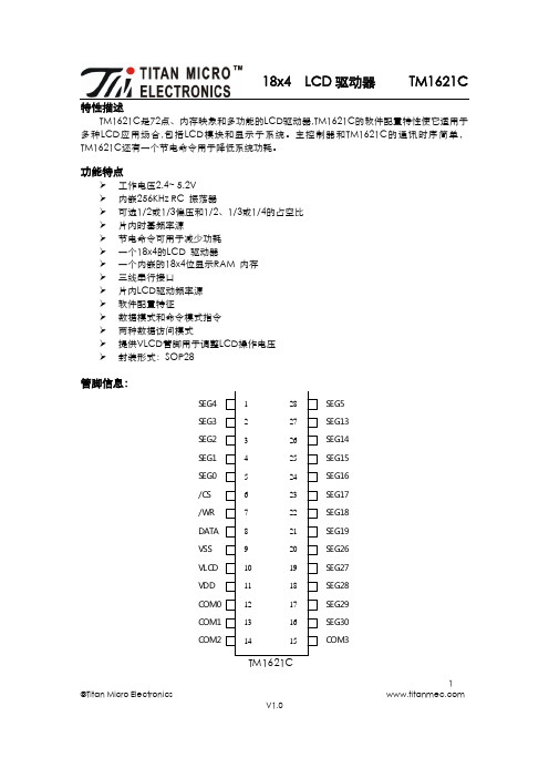
引脚驱动波形
给出使用 1/4 复用,1/3 偏压驱动下显示“2”的波形:
3、LCD驱动器
TM1621C是一个72(18x4)点的LCD驱动器,它可由软件配置成1/2或1/3的LCD驱动器
偏压和2、3或4个公共端口,这一特性使TM1621C适用于多种LCD应用场合。LCD驱动时钟由
系统时钟分频产生,LCD驱动时钟的频率值保持为256Hz,由内RC振荡器产生。LCD驱动器相
管脚信息:
SEG4 SEG3 SEG2 SEG1 SEG0 /CS /WR DATA VSS VLCD VDD COM0 COM1 COM2
圣邦微基准电压
圣邦微基准电压圣邦微基准电压是一种非常重要的电子元器件,它在各种电路中起着至关重要的作用。
它能够提供一个稳定可靠的参考电压,以确保电路中其他元器件的正常工作。
让我们来了解一下什么是微基准电压。
微基准电压是一种非常稳定的电压源,其输出电压几乎不受温度、供电电压和负载变化的影响。
这使得微基准电压成为许多精密电子设备的理想选择,例如模拟电路、传感器和精密测量设备等。
圣邦微基准电压是市场上非常知名的品牌之一。
它以其高精度、低漂移和低噪声等特点而闻名。
圣邦微基准电压的设计和制造经验丰富,确保了其高可靠性和长寿命。
它广泛应用于各种场合,满足了许多关键应用的需求。
与其他品牌的微基准电压相比,圣邦微基准电压具有许多独特的优势。
首先,它采用了先进的工艺技术和精密的电路设计,以确保高精度和低噪声。
其次,它具有良好的温度稳定性和供电电压依赖性,可以在广泛的工作温度范围内提供稳定的输出电压。
此外,圣邦微基准电压还具有良好的负载能力和抗干扰能力,能够适应复杂的工作环境。
除了高性能和可靠性,圣邦微基准电压还注重产品的可定制性和灵活性。
它提供了多种封装和电压范围选择,以满足不同应用的需求。
无论是在工业控制系统、医疗设备还是通信设备中,圣邦微基准电压都能够提供稳定可靠的参考电压。
圣邦微基准电压是一种非常重要的电子元器件,具有高精度、低漂移和低噪声等特点。
它广泛应用于各种电路中,确保电路的正常工作。
作为市场上知名的品牌之一,圣邦微基准电压以其高可靠性和长寿命而备受推崇。
无论在哪个领域,圣邦微基准电压都能够提供稳定可靠的参考电压,满足各种应用的需求。
- 1、下载文档前请自行甄别文档内容的完整性,平台不提供额外的编辑、内容补充、找答案等附加服务。
- 2、"仅部分预览"的文档,不可在线预览部分如存在完整性等问题,可反馈申请退款(可完整预览的文档不适用该条件!)。
- 3、如文档侵犯您的权益,请联系客服反馈,我们会尽快为您处理(人工客服工作时间:9:00-18:30)。
1.270(BSC)
0.400
1.270
0°
8°
Dimensions In Inches
Min
Max
0.053
0.069
0.004
0.010
0.053
0.061
0.013
0.020
0.007
0.010
0.386
0.402
0.150
0.157
0.228
0.244
0.050(BSC)
0.016
0.050
Idol
Vdo = 0.4V
SG 通道电流一致性
△Iolc
SG0~SG7
静态电流损耗
IDDdyn
无负载
最小值
29 145 4 — —
TM3130 典型值
30 160 — ±3 —
最大值
31 — — ±5 5
单位
mA mA mA % mA
开关特性
在-20℃~+85℃下测试,除非另有说明 VDD = 4.5~5.5 V
GR2 GR1 GR0 SG0 SG1 SG2 SG3 SG4 SG5 SG6 SG7
15 10
7 4 5 3 6 14 11 13 12
15 10
7 4 5 3 6 14 11 13 12
15 10
7 4 5 3 6 14 11 13 12
图7
在实际应用中,一般将芯片按照图 7 所示级联以驱动更多的 LED 灯,为防止产品在测试时带电插拔 产生的瞬间高压导致芯片信号输入输出引脚损坏,应该在信号输入的第一颗芯片及输出的最后一颗芯片 串接 100Ω保护电阻,如图中 R1、R2 所示。
—
3.5 — — — — —
TM3130 典型值
800 500
— — — — —
最大值
—
6.5 300 100 100 120 15
单位
KHz μs μs ns ns ns ns pF
©Titan Micro Electronics
V1.0
3
时序特性
LED 恒流驱动专用电路 TM3130
©Titan Micro Electronics
V1.0
5
应用信息
LED 恒流驱动专用电路 TM3130
TM3130适合显示屏驱动或数码管驱动,应用电路如下所示:
VDD 104
VDD 104
VDD 104
MCU端口 R1 9 DIN
16
1
GND VDD IC1
DO 8
内置上电复位电路 通过一根信号线即可完成数据的接收与解码 数据发送速率800Kbps GR 端口扫描频率 2KHz 适用领域:显示屏驱动、数码管驱动等 封装形式:SOP16
内部结构框图
DIN VDD GND
管脚排列
©Titan Micro El
采用高压功率CMOS工艺 SG端口恒流输出30mA VDD工作电压支持4.5~5.5V 8×4显示扫描模式 单线串行级联接口 内置RC振荡并根据数据线上信号进行时钟同步,在接收完本单元数据后能自动将后续数据整形
并通过数据输出端发送至下级,信号不随级联变远而出现失真或衰减
0°
8°
All specs and applications shown above subject to change without prior notice. (以上电路及规格仅供参考,如本公司进行修正,恕不另行通知。)
©Titan Micro Electronics
V1.0
7
整形转发 恒流驱动 扫描输出
图1
VDD
1
16
GND
GR3
2
15
GR2
SG2
3
14
SG4
SG0
4 Top View 13
SG6
SG1
5
12
SG7
SG3
6
11
SG5
GR0
7
10
GR1
DO
8
9
DIN
图2
V1.0
DO SG0 SG7 GR0 GR3
1
管脚功能
引脚名称
VDD SG0~SG7 GR0~GR4
逻辑 0 T0H
Vih Vil
DIN
T
Tplz
T0H'
DO
逻辑 1 T1H
T T1H'
图4
Reset信号 Treset
Reset信号
功能说明
芯片采用单线通讯方式,采用归零码的方式发送信号。芯片上电复位以后,接收DIN端发来的数据, 接收够32bit后,DO端开始转发数据,为级联的下一颗芯片提供输入数据。在转发之前,DO端一直拉低。 如果DIN端输入Reset信号,芯片将接收到的数据送显示,并在该信号结束后重新接收新的数据,接收完 开始的32bit数据后,通过DO端转发后续数据,芯片在没有接收到Reset信号前,SG端口原输出保持不变, 接收到低电平Reset信号后,芯片根据刚才接收到的32bit数据更新SG端口输出。
GND DIN DO
引脚序号
1 3~6,11~14
7,10,15,2 16 9 8
输入输出等效电路
VDD
LED 恒流驱动专用电路 TM3130
I/O
功能说明
--
电源正
O
灌电流恒流驱动
O
拉电流扫描输出
--
电源地
I
数据输入
O
数据输出
VDD
DIN
DO/SGn/GRn
GND
GND
图3
集成电路系静电敏感器件,在干燥季节或者干燥环境使用容易产生大量静电,静电放电可能 会损坏集成电路,天微电子建议采取一切适当的集成电路预防处理措施,不正当的操作和焊 接,可能会造成 ESD 损坏或者性能下降, 芯片无法正常工作。
--
μs
Reset码,低电平时间
Treset
--
200
--
μs
注意: 1、发送 0 码或 1 码的周期时间为 1.25μs(频率 800KHz),字节之间的低电平时间不要超过 45μs,否 则芯片可能复位,复位后又重新接收数据,无法实现数据正确传送; 2、0 码控制相应驱动端口关断,1 码控制相应驱动端口开通。
此外,图中各芯片的 104 退耦电容不可缺少,且走线到芯片的 VDD 和 GND 脚应尽量短,以达到最佳 的退耦效果,稳定芯片工作。
©Titan Micro Electronics
V1.0
6
封装示意图(SOP16)
LED 恒流驱动专用电路 TM3130
A
A2
C
L
θ
极限参数
参数名称
参数符号
极限值
单位
逻辑电源电压
VDD
+7.0
V
逻辑输入电压
Vih
VDD + 0.5
V
功率损耗
PD
400
mW
工作温度
Topt
-40 ~ +85
℃
储存温度
Tstg
-55 ~ +150
℃
人体模式(HBM)
2000
V
ESD
机器模式(MM)
200
V
(1)以上表中这些等级,芯片在长时间使用条件下,可能造成器件永久性伤害,降低器件的可靠性。 我们不建议在其它任何条件下,芯片超过这些极限参数工作; (2)所有电压值均相对于系统地测试。
A1
D
b
e
E1
E
Symbol
A A1 A2 b c D E E1 e L θ
Dimensions In Millimeters
Min
Max
1.350
1.750
0.100
0.250
1.350
1.550
0.330
0.510
0.170
0.250
9.800
10.200
3.800
4.000
5.800
6.200
B2
B1
B0
GR1
B15
B14
B13
B12
B11
B10
B9
B8
GR2
B23
B22
B21
B20
B19
B18
B17
B16
GR3
B31
B30
B29
B28
B27
B26
B25
B24
3、数据接收和转发
图5 其中S1为控制器发送的数据,S2、S3、S4为级联TM3130转发的数据。
数据刷新周期1
数据刷新周期2
S1 D1 D2 D3 D4 … Dn Reset D1 D2 D3 D4 … Dn Reset
©Titan Micro Electronics
V1.0
2
推荐工作条件
LED 恒流驱动专用电路 TM3130
在-20℃~+85℃下测试,除非另有说明
参数名称
参数符号 测试条件
逻辑电源电压
VDD
—
高电平输入电压
Vih
—
低电平输入电压
Vil
—
TM3130
最小值 典型值 最大值
4.5
5
5.5
0.7VDD
—
VDD
0
—
1.35
单位
V V V
电气特性
在-20℃~+85℃下测试,除非另有说明 VDD = 4.5~5.5 V
参数名称
参数符号 测试条件