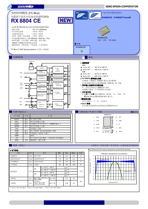
爱普生(EPSON)实时时钟模块RTC-7301SF规格书
爱普生(EPSON)实时时钟模块RA8803SA规格书
DTCXO,
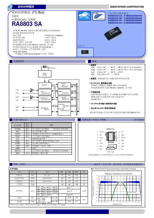
RA8803 SA
• 32.768 kHz
(
) DTCXO
•1/100s •
: I2C-Bus (400kHz)
•
: 1.6 V ~ 5.5 V
•
: 2.2 V ~ 5.5 V
•
: 1.6 V ~ 5.5 V
•
32.768 kHz, 1024 Hz, 1Hz.
•
,
,
,EVIN
FOE FOUT EVIN / INT
SDA SCL
32.768 kHz
32kHz DTCXO
DIVIDER
FOUT CONTROLLER
INTERRUPT CONTROLLER
INTERFACE CIRCUIT
CLOCK and
CALENDAR
TIMER REGISTER
ALARM REGISTER
5 32.768 kHz DTCXO
0
-5
-10
-15 Tuning fork X'tal
-20
-25
-30 -45 -35 -25 -15 -5 5 15 25 35 45 55 65 75 85 Temperature (ºC)
推进环境管理体系 符合国际标准
在环境管理体系的运行方面,使用 ISO14001 国际环境标准,通过“计 划-实施-检查-验证(PDCA)的循环来实现持续改进。公司位于日本和 海外的主要制造基地已取得了 ISO14001 资格认证。
CONTROL REGISTER and
SYSTEM CONTROLLER
T1(CE)
SCL
FOUT
TEST
EPSON 实时时钟芯片RX-8010SJ Application Manual介绍
根据实际功能设置 1F[h]寄存器 使 STOP=‘0’
继续其它操作
RX-8010SJ 13
13.1
通过 I2C 总线接口读写数据
器件地址(Device Address/Slave Address) 所有的通讯操作都是以 [START 条件] + [从设备地址 + (R/W 读写选择)开始的。 从设备地址如下:
RX-8010SJ
12.3.2 固定周期定时中断寄存器 相关寄存器:
* 在进入操作设定之前,建议将 TE 位 清 0。 * 在不用该功能的时候,计数器 0,1 可以作为 RAM 来使用,但需要将 TE 和 TIE 清 0。 1)用于固定定时器的递减计数器 0,1 该寄存器用来设定定时器的默认值, 从 0 到 65535。 在写入预设值之前请确认 TE 位 为’0’。 *TE 为‘0’时读出来的值是预设值, ‘1’时读出来的值是计数值。 2)TSEL0,TSEL1,TSEL2 这三个位的组合用来设置倒数计数的周期(时钟源)
RX-8025T规格书(中文)
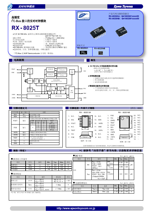
• 多种检测功能 • 电源电压监控功能 (具有可选择的检测阈值)
• 停止检测功能
• 加电重设检测功能
• 警报器功能和定时器功能
SCL
• 产生周期性的中断信号定时器功能。
及可任意组合星期 , 时 , 分 , 钟设定的警报功能
SDA
GND
引脚功能定义
信号名称 SCL SDA
FOUT
FOE
/ INTA / INTB TEST
:1.15 V ~ 5.5 V
•多种检测功能
:如,振荡停止检测功能
•低待机电流
:0.48 µA / 3 V (Typ.)
•32.768 kHz 频率输出功能
:带控制引脚的 C-MOS 输出
•包括时刻、日历、各种检测功能、中断功能等
* I2C-Bus 是 NXP Semiconductor 公司的一种商标。
警报器_D 寄存器 (分,时)
时间计数器 (秒,分,时,周,日,月,年)
电压 检测
OSC 检测
中断控制
地址 解码器
地址 寄存器
移位寄存器
I/O 控制
概览
• 32.768 kHz 石英振荡器的内置功能 •频率已针对高精度调整。
VDD
( ± 5 ×10⁻⁶ / Ta = +25 °C ) ( 相当于每月 13 秒的偏差 )
0.5 6.3 Max.
RX − 8025 NB
22. N.C. 21. N.C.
4.8 5.0 ± 0.2
20. 19. ห้องสมุดไป่ตู้8. 17. 16. 15.
1.3 ± 0.1
14. 13. 12.
N.C. N.C. N.C. N.C. N.C. N.C. N.C.
爱普生(EPSON)实时时钟模块RA4803SA规格书
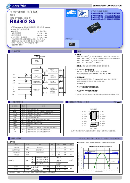
DIVIDER
FOUT CONTROLLER
INTERRUPT CONTROLLER
INTERFACE CIRCUIT
CLOCK and CALENDAR
TIMER REGISTER
ALARM REGISTER
SYSTEM CONTROLLER
and CONTROL REGISTER
• •UA •UB •UC •AA
± 3.4 x 10⁻⁶ / -40 ºC ~ +85 ºC 商
± 5.0 x 10⁻⁶ / -40 ºC ~ +85 ºC 商 ± 5.0 x 10⁻⁶ / -30 ºC ~ +70 ºC (+5 ± 5.0) x 10-6 / +25 ºC
9
器
13
器
•
:
1/100s
●为汽车行驶安全方面的应用(引擎控制单元、气囊、电子稳定程序控制系统)。
注意事项
·本材料如有变更,恕不另行通知。量产设计时请确认最新信息。 ·未经 Seiko Epson 公司书面授权,禁止以任何形式或任何方式复制或者发布本材料中任何部分的信息内容。 ·本材料中的书面信息、应用电路、编程、使用等内容仅供参考。Seiko Epson 公司对第三方专利或版权的侵权行为不负有任何责任。本材料
0
-5
-10
-15 Tuning fork X'tal
-20
-25
-30 -45 -35 -25 -15 -5 5 15 25 35 45 55 65 75 85 Temperature (ºC)
推进环境管理体系 符合国际标准
在环境管理体系的运行方面,使用 ISO14001 国际环境标准,通过“计 划-实施-检查-验证(PDCA)的循环来实现持续改进。公司位于日本和 海外的主要制造基地已取得了 ISO14001 资格认证。
Seiko Epson RTC-4543SA SB实时时钟模块应用手册说明书

ETM09E-03Real Time Clock ModuleRTC-4543SA/SB•These products are intended for general use in electronic equipment. When using them in specific applications that require extremelyobtain permission from Seiko Epson in advance./ Space equipment (artificial satellites, rockets, etc.) / Transportation vehicles and related(automobiles, aircraft,Submarine transmitters / Power stations and related / Fire work equipment and securityequipment / traffic control equipment / and others requiring equivalent reliability.•All brands or product names mentioned herein are trademarks and/or registered trademarks of their respective.CONTENTS1. OVERVIEW (1)2. BLOCK DIAGRAM (1)3. PIN CONNECTIONS (2)4. PIN FUNCTIONS (2)5. ELECTRICAL CHARACTERISTICS (3)5-1.A BSOLUTE M AXIMUM R ATINGS (3)5-2.O PERATING C ONDITION (3)5-3.F REQUENCY C HARACTERISTICS (3)5-4.DC C HARACTERISTICS (3)5-5.AC C HARACTERISTICS (4)5-6.T IMING C HARTS (5)6. TIMER DATA ORGANIZATION (6)7. DESCRIPTION OF OPERATION (7)7-1.D ATA READS (7)7-2.D ATA WRITES (7)7-3.D ATA WRITES (D IVIDER R ESET) (8)7-4.FOUT OUTPUT AND 1H Z CARRIES (8)8. EXAMPLES OF EXTERNAL CIRCUITS (9)9. EXTERNAL DIMENSIONS (10)10. LAYOUT OF PACKAGE MARKINGS (10)11. REFERENCE DATA (11)12. APPLICATION NOTES (12)32-kHz Output Serial RTC ModuleRTC - 4543 SA/SBBuilt-in crystal permits operation without requiring adjustmentBuilt-in time counters (seconds, minutes, hours) and calendar counters (days, days of the week months, years)Operating voltage range: 2.5 V to 5.5 VSupply voltage detection voltage: 1.7 ±0.3 VLow current consumption: 1.0 µA/2.0 V (Max.)Automatic processing for leap yearsOutput selectable between 32.768 kHz/1 Hz1. OverviewThis module is a real-time clock with a serial interface and a built-in crystal oscillator. This module is also equipped with clock and calendar circuits, an automatic leap year compensation function, and a supply voltage detection function.In addition, this module has a 32.768 kHz/1 Hz selectable output function for hardware control that is independent of the RTC circuit.This module is available in a compact SOP 14-pin package (RTC-4543SA) and a thin SOP 18-pin package (RTC-4543SB).4. Pin FunctionsSignalPin No.SOP-14pin(SOP-18pin)I/O FunctionGND1( 9 )Connects to negative (-) side (ground) of the power supply.CE3( 8 )InputChip enable input pin.When high,the chip is enabled. When low,the DATA pin goes tohigh impedance and the CLK,DATA,and WR pins are not able toaccept input.In addition, when low,the TM bit is cleared.FSEL4( 7 )InputSerect the frequency that is output from the FOUT pin.High : 1 HzLow : 32.768 kHzWR5( 6 )InputDATA pin input/output switching pin.High : DATA input (when writing the RTC)Low : DATA output (when reading the RTC)FOE6( 5 )InputWhen high, the frequency selected by the FSEL pin is output fromthe FOUT pin.When low, the FOUT pin goes to high impedance.V DD9( 14 )Connects to positive (+) side of the power supply.CLK10( 12 )InputSerial clock input pin.Data is gotten at the rising edge during a write, and data is outputat the rising edge during a read.DATA11( 11 )Bi-directional Input/outout pin that is used for writing and reading data.FOUT14( 10 )OutputOutputs the frequency selected by the FSEL pin. 1 Hz output issynchronized with the internal one-second signal.This output is not affected by the CE pin.N.C.2,7,8,12,13( 1,2,3,4,13,15,16,17,18 )Although these pins are not connected internally,they shouldalways be left open in order to obtain the most stable oscillationpossible.* Always connect a passthrough capacitor of at least 0.1 µF as close as possible between V DD and GND.5. Electrical Characteristics5-1. Absolute Maximum RatingsItem Symbol Conditions Min. Max. Unit Supply voltage V DD-0.3 7.0 VInput voltage V I Ta=+25 °C GND-0.3 V DD+0.3 VOutput voltage V O GND-0.3 V DD+0.3 V Storage temperature T STG- -55 +125 °C5-2. Operating ConditionItem Symbol Conditions Min. Max. Unit Operating supplyV DD- 2.5 5.5 V voltageData holding voltage V CLK- 1.4 5.5 VOperating temperature T OPR No condensation-40 +85 °C5-3. Frequency CharacteristicsItem Symbol Conditions Max. Unit Frequency tolerance ∆f/f O Ta=+25 °C , V DD=5.0 V 5 ± 23 * ×10-6Frequency temperatureT op-10to+70 °C +25 °C ref + 10 / - 120 ×10-6 characteristicsFrequency voltagef/V Ta=+25 °C , V DD=2.0 to 5.5 V ± 2 ×10⁻⁶/V characteristicsOscillation start time t STA Ta=+25 °C , V DD=2.5 V 3 s Aging fa Ta=+25 °C , V DD=5 V , first year ± 5 ×10⁻⁶ * Monthly deviation: Approx. 1 min.5-4. DC CharacteristicsUnless specified otherwise: V DD = 5 V ± 10 %, Ta = - 40 to +85 °C Item Symbol Conditions Min. Typ. Max. Unit Current consumption(1) I DD1 V DD=5.0 V CE=L , FOE=L 1.5 3.0 µA Current consumption(2) I DD2 V DD=3.0 V FSEL=H 1.0 2.0 µA Current consumption(3) I DD3 V DD=2.0 V 0.5 1.0 µA Current consumption(4) I DD4 V DD=5.0 V CE=L , FOE=H 4.0 10.0 µA Current consumption(5) I DD5 V DD=3.0 V FSEL=L 2.5 6.5 µA Current consumption(6) I DD6 V DD=2.0 V No load on the1.5 4.0 µAFOUT pinInput voltage V IH WR,DATA,CE,CLK, 0.8 V DD VV IL FOE,FSEL pins 0.2 V DD V0.5 µAInput off/leak current I OFF WR,CE,CLK,FOE,FSEL pinsV IN = V DD or GNDV OH(1)V DD=5.0 V I OH=-1.0 mA 4.5 V Output voltage V OH(2)V DD=3.0 V DATA , FOUT pins 2.0 VV OL(1)V DD=5.0 V I OL= 1.0 mA 0.5 VV OL(2)V DD=3.0 V DATA , FOUT pins0.8 VOutput load conditionN / CL FOUT pin 2 LSTTL / 30 pF Max.( fanout )Output leak current I OZH V OUT=5.5 V DATA , FOUT pins-1.0 1.0 µAI OZL V OUT=0 V DATA , FOUT pins-1.0 1.0 µASupply voltage detectionV DT- 1.4 1.7 2.0 V voltage5-5. AC CharacteristicsUnless specified otherwise: Ta = - 40 to +85 °C, CL = 50 pF Item Symbol V DD=5 V ± 10 % V DD=3 V ± 10 % UnitMin. Max. Min. Max.CLK clock cycle t CLK0.75 7800 1.5 7800 µsCLK low pulse width t CLKL0.375 3900 0.75 3900 µsCLK high pulse width t CLKH0.375 3900 0.75 3900 µs CLK setup time t CLKS25 50 nsCE setup time t CES0.375 3900 0.75 3900 µsCE hold time t CEH0.375 0.75 µsCE enable time t CE0.9 0.9 s Write data setup time t SD0.1 0.2 µsWrite data hold time t HD0.1 0.1 µs WR setup time t WRS100 100 nsWR hold time t WRH100 100 ns DATA output delay time t DATD0.2 0.4 µsDATA output floating time t DZ0.1 0.2 µs Clock input rise time t r150 100 nsClock input fall time t f150 100 ns FOUT rise time (CL=30 pF) t r2100 200 ns FOUT fall time (CL=30 pF) t f2100 200 ns Disable time (CL=30 pF) t XZ100 200 nsEnable time (CL=30 pF) t ZX100 200 nsFOUT duty ratio (CL=30 pF) Duty 40 60 40 60 % Wait time t RCV0.95 1.9 µs5-6. Timing Charts[]Duty t t100%H=×( 4 ) Disable/enable6. Timer Data Organization• The counter data is BCD code.• Writes and reads are both performed on an LSB-first basis.MSBLSBSecond ( 0 to 59 )FDTs40s20s10s8s4s2s1Minutes ( 0 to 59 ) * mi40mi20mi10mi8mi4mi2mi1Hour ( 0 to 23 ) * *h20h10h8h4h2h1Day of the week( 1 to 7 )*w4w2w1Day ( 1 to 31 ) * *d20d10d8d4d2d1Month ( 1 to 12 ) TM **mo10mo8mo4mo2mo1Year ( 0 to 99 )y80y40y20y10y8y4y2y1• Calendar counter. From 1 Jan 2001 to 31 Dec 2099, it is updated by an automatic calendar function.If a year is 4 multiples, it is a leap year, then date is updatedin order to 28 Feb, 29 Feb, Mar 1.Because there is the case that a leap year does not match when using data of year of except the Christian era, please be careful.Data of a day of the week run in cycles with 7 from 1.A recommended example are 1=Sun, 2=Mon,,,6=Fri, 7=Sat.• Clock counter. Only 24 hours system is supported. • ∗bits. These bits are used as memory.• TM bit. This is a test bit for shipping test. Always clear this bit to “0”.• FDT bit: Supply voltage detection bit• This bit is set to “1” when voltage of 1.7 ±0.3 V or less is detected between V DD and GND. • The FDT bit is cleared if all of the digits up to the year digits are read.• Although this bit can be both read and written, clear this bit to "0" in case of the write cycle.if the supply voltage is lower than the detection voltage value, the FDT bit is set to “1”.7. Description of Operation2) At the first rising edge of the CLK signal, the clock and calendar data are loaded into the shiftregister and the LSB of the seconds digits is output from the DATA pin.3) The remaining seconds, minutes, hour, day of the week, day, month, and year data is shifted out,in sequence and in synchronization with the rising edge of the CLK signal, so that the data isoutput from the DATA pin.The output data is valid until the rising edge of the 52nd clock pulse; even if more than 52 clockpulses are input,the output data does not change.4) If data is required in less than 52 clock pulses, that part of the data can be gotten by setting theCE pin low after the necessary number of clock pulses have been output.Example: If only the data from “seconds” to “day of the week” is needed:After 28 clock pulses, set the CE pin low in order to get the data from “seconds” to “day ofthe week.”5) When performing successive data read operations, a wait (tRCV) is necessary after the CE pinis set low.6) Note that if an update operation (a one-second carry) occurs during a data read operation,the data that is read will have an error of -1 second.7) Complete data read operations within tCE (Max.) = 0.9 seconds, as described earlier.1) RTC 4543 shifts to data input state by condition of WR terminal ="H",CE terminal ="H".2) Writing-data synchronize to a rising edge of CLK, and it inputs into an RTC from LSB of sec.3) Inside counter less than second is reset between falling edges of first CLK from a rising edge of next CLK.And update of Clock register is prohibited by the first falling edge of CLK.4) In writing of data to RTC, all 52 clock is necessary.When CE goes to LOW before the 52 bits transmission is completed, there is the possibilitythat * ,FDT and a year digit were destroyed.If a serial communication break occurs, do verify 8 bits of* bit andFDTbit and year data.5) In a rising edge of 52 clock, all data is written to RTC. Data after 53 bits is ignored.6) When CE goes to LOW, RTC re-starts update.Please finish write access within 0.9 second = tCE (Max.).7) Between write access and read access, recovery timing(tRCV) is necessary.Please do not set the time and date which is non-existence.7-3. Data writes (Divider Reset)After the counter is reset, carries to the seconds digit are halted.After the data write operation,the prohibition on carries to the seconds counter is lifted by setting the CE pin low.Complete data write operations within tCE (Max.) = 0.9 seconds, as described earlier.7-4. FOUT output and 1 Hz carriesDuring a data write operation, because a reset is applied to the Devider counter (from the 128 Hzlevel to the 1 Hz level) after the CE pin goes high during the time between the falling edge of the first clock cycle and the rising edge of the second clock cycle, the length of the first 1 Hz cycle after thedata write operation is 1.0 s +0 / −7.8ms +t CES+t CLK. Subsequent cycles are output at1.0-second intervals.The 1-Hz signal that is output on FOUT is the internal 1-Hz signal with a 15.6-ms shift applied.8. Examples of External Circuits11. Reference DataNote : This data shows values obtained from a sample lot.12. Application notes1) Notes on handlingThis module uses a C-MOS IC to realize low power consumption. Carefully note the following cautions when handling.(1) Static electricityWhile this module has built-in circuitry designed to protect it against electrostatic discharge, the chip could still be damaged bya large discharge of static electricity. Containers used for packing and transport should be constructed of conductive materials.In addition, only soldering irons, measurement circuits, and other such devices which do not leak high voltage should be used with this module, which should also be grounded when such devices are being used.(2) NoiseIf a signal with excessive external noise is applied to the power supply or input pins, the device may malfunction or "latch up."In order to ensure stable operation, connect a filter capacitor (preferably ceramic) of greater that 0.1 µF as close as possible to the power supply pins (between VDD and GNDs). Also, avoid placing any device that generates high level of electronic noise near this module.* Do not connect signal lines to the shaded area in the figure shown in Fig. 1 and, if possible, embed this area in a GND land.(3) Voltage levels of input pinsWhen the input pins are at the mid-level, this will cause increased current consumption and a reduced noise margin, and can impair the functioning of the device. Therefore, try as much as possible to apply the voltage level close to VDD or GND.(4) Handling of unused pinsSince the input impedance of the input pins is extremely high, operating the device with these pins in the open circuit state can lead to unstable voltage level and malfunctions due to noise. Therefore, pull-up or pull-down resistors should be provided for all unused input pins.2) Notes on packaging(1) Soldering heat resistance.If the temperature within the package exceeds +260 °C, the characteristics of the crystal oscillator will be degraded and it may be damaged. The reflow conditions within our reflow profile is recommended. Therefore, always check the mounting temperature and time before mounting this device. Also, check again if the mounting conditions are later changed.* See Fig. 2 profile for our evaluation of Soldering heat resistance for reference.(2) Mounting equipmentWhile this module can be used with general-purpose mounting equipment, the internal crystal oscillator may be damaged in some circumstances, depending on the equipment and conditions. Therefore, be sure to check this. In addition, if the mounting conditions are later changed, the same check should be performed again.(3) Ultrasonic cleaningDepending on the usage conditions, there is a possibility that the crystal oscillator will be damaged by resonance during ultrasonic cleaning. Since the conditions under which ultrasonic cleaning is carried out (the type of cleaner, power level, time, state of the inside of the cleaning vessel, etc.) vary widely, this device is not warranted against damage during ultrasonic cleaning.(4) Mounting orientationThis device can be damaged if it is mounted in the wrong orientation. Always confirm the orientation of the device before mounting.(5) Leakage between pinsLeakage between pins may occur if the power is turned on while the device has condensation or dirt on it. Make sure the device is dry and clean before supplying power to it.Application ManualElectronic devices information on WWW serverDistributor/en/quartz/index.html。
爱普生高端工程投影机说明书
●
4500流明色彩亮度,可投射大画面● 分辨率XGA,呈现高清晰的图像
● 高画质,采用爱普生原创水晶高清技术● 高可靠,采用爱普生原创无机液晶面板● 镜头可位移
● 多种图像校正方式
爱普生高端工程投影机
EVS130504BZ
图片仅供参考,外观以实物为准。
本说明若有任何细节之更改,恕不另行通知。
爱普生(中国)有限公司在法律许可的范围内对以上内容有解释权。
爱普生(中国)有限公司
北京市东城区金宝街89号金宝大厦7层 官方网站: 服务导购热线:400-810-9977官方微博:@爱普生中国/epsoncn 官方微信:爱普生中国爱普生解决方案体验中心:
北京:北京市东城区金宝街89号金宝大厦610室
电话:010-8522-1186广州:广州市天河区天河路230号万菱国际中心1308室
电话:020-2863-3128上海:上海市漕河泾开发区宜山路900号科技大厦B 区607室 电话:021-5423-4478沈阳:沈阳市和平区和平北大街65号总统大厦C 座20层2003室 电话:024-6215-0090西安:西安市南大街30号中大国际大厦C 座C301室
电话:029-8720-3001
官方微博
(扫描二维码即可访问)
官方微信
(扫描二维码即可访问)
在之前仅用在高端的家庭影院投影机中的爱普生独有的水晶高清技术,如今首可选的用户吊架突出了设计的平衡,使整个空间设计完好相配。
58%
58%
38%。
爱普生(EPSON)实时时钟模块RTC-4543SA规格书

实际尺寸电路框图概览引脚功能定义引脚连接 / 外部尺寸规格(单位:mm)规格(特征)*请参考“应用手册”章节内容,以获取更多详细信息。
RTC-4543SA实时时钟模块 (SPI-Bus)简单功能 RTC - 4543 SA∙内置32.768 kHz 晶体单元. (频率精度调整完毕) ∙接口类型 :3线串行接口 ∙工作电压范围 :2.5 V ~ 5.5 V ∙宽计时器电压范围 :1.4 V ~ 5.5 V ∙32.768 kHz 频率输出功能 :带控制引脚的CMOS 输出 ∙包括时刻、日历、电压检测功能等产品号码(请联系我们)RTC-4543SA : Q41454352000200 RTC-4543SB : Q41454361000200推进环境管理体系 符合国际标准在环境管理体系的运行方面,使用ISO14001国际环境标准,通过“计划-实施-检查-验证(PDCA)的循环来实现持续改进。
公司位于日本和海外的主要制造基地已取得了ISO14001资格认证。
追求高品质Seiko Epson 为了向顾客提供高品质、卓越信赖性的产品、服务,迅速着手通过ISO 9000系列资格认证的工作,其日本和海外工厂也在通过ISO 9001认证。
同时,也在通过大型汽车制造厂商要求规格的ISO/TS 16949认证。
关于在目录内使用的记号●无铅。
●符合欧盟RoHS 指令。
欧盟RoHS 指令免检的含铅产品。
(密封玻璃、高温熔化性焊料或其他材料中包含铅。
)●为汽车方面的应用,如汽车多媒体、车身电子、遥控无钥门锁等。
●为汽车行驶安全方面的应用(引擎控制单元、气囊、电子稳定程序控制系统)。
注意事项·本材料如有变更,恕不另行通知。
量产设计时请确认最新信息。
·未经Seiko Epson 公司书面授权,禁止以任何形式或任何方式复制或者发布本材料中任何部分的信息内容。
·本材料中的书面信息、应用电路、编程、使用等内容仅供参考。
进口晶振料号、尺寸大全.xls
KHZSPXOTCO-710x SeriesSG-770/771TCO-708x Series SG-615/531/51 Series SG-645/636 Series SG-310Series SG-550 Series SG-211SxE SG-3030/3040SG-210SxD SG-210SxH SG-150SxE SG-210 SxB MC-306/405/406 MC-30A爱普生压控温补振荡器HG-2150CASeries FC-13A FC-13F/135/255MC-146/156爱普生晶振晶体单元FC-12D/12MC-TYPE/C-2-TYPE/C-4-TYPE串行RX-8581SA/JE/NB RX-8731LC RX-8803SA/LCRX-5412SF RX-8025SA/NB RX-8571SA/NB/LC RX-4575LC RX-4581NB RX-4803SA/LC RX-4571LC/NB/SA RX-4574LC RTC-8564JE/NB/RX-8564LC RX-4045SA/NBRTC-4543SA/SB RTC-4574SA/JE/NB RTC-4701JE/NBRA-4574SA RA-8565SA RA-8581SA 爱普生实时钟模块32.768KHZRA-4565SA音叉型水晶振动子KHKDS表面封装型振水晶振动子MHZUM-5HC-49/UAT-49UM-4AT-38UM-1SMD-49DMX-38DSX840GA DSX840GT DSX151GAL DSX531SDSX630G DSX321SH DSX530GA DSX321G DSX321SL DSX211AL DSX221SHDSX211A DSX221S DSX211G DSX221G KDS晶振DSX1612ADSR221STHKDS振荡器DSA211SCL (VC-TCXO)DSB211SCL (TCXO)DSB211SCB (TCXO)DSA211SDA (VC-TCXO)DSB211SDA (TCXO)DSB211SDB (TCXO)DSA211SDT (VC-TCXO)DSB211SDT (TCXO)DSA222MAA (VC-TCXO)DSA222MAB (VC-TCXO)DSB222MAA (TCXO)DSB222MAB (TCXO)DSA221SCL (VC-TCXO)DSB221SCL (TCXO)DSB221SCB (TCXO)DSA221SDA (VC-TCXO)DSB221SDB (TCXO)DSB221SDA (TCXO)DSA221SDT (VC-TCXO)DSB221SDT (TCXO)DSA221SJ (VC-TCXO)DSB221SJ (TCXO)DSA321SCL (VC-TCXO)DSB321SCL (TCXO)DSV221SR (1.8V動作タイプ)(VCXO)DSV221SV (2.8V/3.3V 動作タイプ) (VCXO)DSV321SR (1.8V動作タイプ) (VCXO)DSV321SV (2.8V/3.3V 動作タイプ) (VCXO)DSV323SD (HCSL出力) (VCXO)DSV323SJ (LVDS出力) (VCXO)DSV323SK (LV-PECL出力) (VCXO)DSV753HJ (LVDS出力) (VCXO)DSV753HK (LV-PECL出力) (VCXO)DSV753SJ (LVDS出力)(VCXO)DSS753SVC(SSXO)CITIZEN晶振西铁城KHZ晶振CFS-206CMR200TCFS-145CMJ206TCFV-206CM250C西铁城MHZ晶振CSA-310CSA-309HCM49CM309SCS325SCSX-750F CSX-750P CSX-750VNX2012SANX3215SAKHZ谐振器音叉晶振RV-2123-C2精工晶振日本NDK晶振振荡器RV-3029-C2-A RV-3029-C2-BRV-3049-C2-A RV-3049-C2-A RV-3049-C2-B 西铁城晶振振荡器瑞士微晶RV-4162-C7RV-8564-C2NX3215SA NX1612AA NX1612AANX2016SA NX2520SA NX3225GANX5032GA NX5032SA NX1255GB NR-2BNR-2C AT-41CD2京瓷晶振KHZ音叉型号频率尺寸ST2012SB 32.768K 2.0 x 1.2 x 0.6ST3215SB 32.768K3.2 x 1.5 x 0.8石英晶体振荡器KC2520B 32.768K 2.5 x 2.0 x 0.7KC2520M 32.768K 2.5 x 2.0 x 0.7温度-40-125°KC3215A32.768K3.2 x 1.5 x 1.0温度补偿水晶振荡器KT3225T 32.768K3.2 x 2.5 x 1.0TCXOCMOS输出类KC2520B-C11.5~1252.5 x 2.0 x 0.7KHZ谐振器M晶体谐振器SPXO钟用晶体振荡器VCXO晶振KC2520B-C2125~160 2.5 x 2.0 x 0.7KC3225A-C21.5~125 3.2 x2.5 x 0.89(K25-2C)KC5032A-CM 1.789~50 5.0 x 3.2 x 1.2KC5032C-C31.8 ~ 170 5.0 x 3.2 x 1.0(K30-3C)KC5032E-C314.31818~166 5.0 x 3.2 x 1.1KC7050A-C21.8~1257.0 x 5.0 x 1.6(K53-2C)石英晶体振荡器(VCXO)KV5032C-C3 1.5~80 5.0 x 3.2 x 1.0KV7050B-C3 1.5~1707.0 x 5.0 x 1.6石英晶体振荡器(TCXO)KT252013~52 2.5 x 2.0 x 0.8max GPS用KT322513~52 3.2 x 2.5 x 1.0max GPS用 台湾晶技(TXC)32.768KHz贴片频率尺寸9HT732.768K 6.9 x 1.4 x 1.30mm9HT932.768K 4.1 x 1.5 x 0.80mm9HT1032.768K 3.2 x 1.5 x 0.75mm9HT1132.768K 2.0 x 1.2 x 0.60mmMHZ9B 3.2 ~ 90MHz11.5 x 5.0 x 3.68mm49/S9C 3.2 ~ 90MHz12.7 x 4.8 x 3.80mm49/SMD 7A8 ~ 80MHz 5.0 x 3.2 x 1.20mm黑色面7B8 ~ 100MHz 5.0 x 3.2 x 0.90mm7M10 ~ 54MHz 3.2 x 2.5 x 0.70mmAV9.9 ~ 54MHz 3.2 x 2.5 x 0.80mm黑色面8Z12 ~ 54MHz 2.5 x 2.0 x 0.55mm石英振荡器7W 1 ~ 170MHz7 x 5 x 1.3mm7C 1 ~ 150MHz 5 x 3.2 x 1.2mm7X 1 ~ 125MHz 3.2 x 2.5 x 1mm8W 4 ~ 54MHz 2.5 x 2 x 0.8mmVCXO 压控振荡器BK60 ~ 700MHz7 x 5 x 1.3mmCJ60 ~ 200MHz 5 x 3.2 x 1.2mmTCXO 温补振荡器7Q13 ~ 52MHz 3.2 x 2.5 x 1mm7L13 ~ 52MHz 2.5 x 2 x 0.8mmNDK(日本电波工业株式会社)晶体谐振器频率尺寸NX2520SG19.2-54MHZ 2.5*2.0*0.9NX3215SA32.768KHZ 3.2*1.5*0.8NX2520SA16-80MHZ 2.5*2.0*0.5NX3225SA12-150MHZ 3.2*2.5*0.55NX3225GA9.840-50MHZ 3.2*2.5*0.75NX5032GB12-55MHZ 5.0*3.2*1.0NX5032GA8-55MHZ 5.0*3.2*1.3NX5032SD9.75-40MHZ 4.9*3.1*0.9AT-41 3.1375-74.1MHZ11.05*4.7*3.6849/S AT-41CD2 3.1375-74.1MHZ11.4*4.8*4.049/SMD晶体振荡器(SPXO)NZ2520SB 1.5 to 80 2.5×2.0×0.9 NZ2520SB 32.768KHZ 2.5×2.0×0.9 2725N 2.5 to 70 5.0×3.2×1.0 2725T 2.5 to 125 5.0×3.2×1.0 7311S-GF-505P62.5-313MHZ7.0*5.0*1.7温补振荡器(TCXO)NT2520SB13.-52MHZ 2.5*2.0*0.9NT3225SA10-40MHZ 3.2*2.5*1.0NT7050BC19.2-26MHZ7.0*5.0*2.0压控振荡器(VCXO)NV2520SA 1.25-80MHZ 2.5*2.0*0.9 NV3225SA 1.25-80MHZ 3.2*2.5*0.9 NV5032SA38.4-52MHZ 5.0*3.2*1.2 NV7050SA 2.048-700MHZ7.0*5.0*1.6晶体滤波器21E15AB21.4MHZ7.0*5.0*1.35 台湾鸿星(HOSONIC)晶体谐振器频率尺寸2SB12~54MHz 2.5*2.0*0.55mm 3SB12~54MHz 3.2*2.5*0.65mm 5SB10~80MHz 5.0*3.2*0.80mm 6SB8~80MHz 6.0*3.5*1.0mm 7SB6~100MHz7.0*5.0*1.1mm 3FB12~54MHz 3.2*2.5*0.80mm5FA10~80MHz 5.0*3.2*1.20mm黑色面两个脚8FA6~80MHz8.0*4.5*1.60mmHC-49SA 3.2~66MHz11.05*4.65*3.50mmHC-49SB8~66MHz11.05*4.65*2.5mmHC-49SMB8~66MHz12.9*4.7*3.2mmHC-49SMA 3.2~66MHz12.9*4.7*4.2mmDT-2630~100KHzDT-3830~100KHz石英振荡器HXO-31~133MHz7.0*5.0*1.5mmHXO-51~133MHz 5.0*3.2*1.3mmHXO-S1~54MHz 3.2*2.5*1.2mmHXO-N1~54MHz 2.5*2.0*0.9mm台湾希华晶振(SIWARD)晶体谐振器频率尺寸LP-2.5 3.5 ~ 80 MHz11.05 x 4.65 x H49/SLP-3.5 3.5 ~ 80 MHz11.05 x 4.65 x HLP-3.5S 3.5 ~ 80 MHz12.3 x 4.7 x H49/SMDLP-4.2S 3.5 ~ 80 MHz12.3 x 4.7 x HSX-252012 ~ 66 MHz 2.5 x 2.0 x 0.55SX-322510 ~ 125 MHz 3.2 x 2.5 x 0.8SX-50328 ~ 100 MHz 5.0 x 3.2 x 0.7SX-60358 ~ 50 MHz 6.0 x 3.5 x 1.0SX-7050 6 ~ 100 MHz7.0 x 5.0 x 1.1GX-3225410 ~ 54 MHz 3.2 x 2.5 x 0.8黑色面四脚GX-503228 ~ 60 MHz 5.0 x 3.2 x 1.1黑色面两脚和四脚GX-50324GX-603528 ~ 60 MHz 6.0 x 3.5 x 1.1黑色面两脚和四脚GX-60354GX-705026 ~ 70 MHz7.0 x 5.0 x 1.4黑色面两脚和四脚GX-70504石英振荡器SHO-3225 2.5 ~ 60 MHz 3.2 x 2.5 x 0.9OSC73 2.5 ~ 60 MHz 5.0 x 3.2 x 1.05OSC57A40 ~ 160 MHz7.0 x 5.0 x 1.5SPO-2520B 1 ~ 200 MHz 2.5x2.0x0.8SPO-3225B 1 ~ 200 MHz 3.2x2.5x0.9SPO-5032B 1 ~ 200 MHz 5.0x3.2x0.9SPO-7050B 1 ~ 200 MHz7.0x5.0x1.4温补振荡器(TCXO)TXO928 ~ 45 MHz 3.2 x 2.5 x 0.9TXO83 6 ~ 45 MHz 5.0 x 3.2 x 1.05STO-2520B0.675 ~ 55 MHz 2.5 x 2.0 x 0.9STO-3225B0.675 ~ 55 MHz 3.2 x 2.5 x 1.0STO-5032B0.675 ~ 55 MHz 5.0 x 3.2 x 1.05STO-7050B0.675 ~ 55 MHz7.0 x 5.0 x 1.4STO-2520A16.368 ~ 38.4 MHz 2.5x2.0x0.8STO-3225A16.368 ~ 27.456 MHz 3.2x2.5x1.0压控温补振荡器(VC-TCXO)VTX7110 ~ 26 MHz7.0 x5.0 x 1.6VTX928 ~ 45 MHz 3.2 x 2.5 x 0.9VTX83 6 ~ 45 MHz 5.0 x 3.2 x 1.05压控振荡器(VCXO)SCV-3225 1.5 ~ 54 MHz 3.2 x 2.5 x 0.9VCX95 1.5 ~ 61.440 MHz 5.0 x 3.2 x 1.1VCX91 1.5 ~ 54 MHz7.0 x 5.0 x 1.6台湾嘉碩(TST)型号频率尺寸TZ0507A32.768K 4.1x1.5x0.25TZ0601A32.768K7.0x1.5x1.4TZ0756A32.768K 6.5x2.0TZ0824A32.768K 4.1x1.5x0.7TZ0853A32.768K8.0x3.8x2.5TZ1006A32.768K 3.2x1.5TZ1021A32.768K 5.2x1.5TZ1692A32.768K 4.9x1.8x1.0TZ2426A32.768K 6.0x2.0TZ2430A 3.997 HC49UTZ0694A4HC49-SMD 以下嘉碩型号 每一个频率都有不同的型号.太多了,只写了几个TZ0195A6M7.0x5.0x1.1TZ0777A8M 5.0x3.2x1.0TZ0994A8M 6.0x3.5x1.1TZ0419A11.0592 MHZ 4.0x2.5x0.8TZ0481A12MHZ 3.2x2.5x0.7石英振荡器TW0357A32.768KHZ 3.2x2.5x1.2TW0190A6MHZ 3.2x2.5x1.2TW0280A10MHZ 5.0x3.2x1.3TW0229A12.288MHZ7.0x5.0x1.9TW0160A13MHZ 5.0x3.2x1.3TW0135A13.5 5.0x3.2x1.2TW0149A14.318184 5.0x3.2x1.3TW0277A16MHZ 3.2x2.5x1.2TW0286A16MHZ7.0x5.0x1.9压控温补振荡器(VC-TCXO)TX0329A10MHZ 3.2x2.5x1.2TX0173A12MHZ 5.0x3.2x1.2台湾加高晶振(HELE)型号频率尺寸HSX221SR 2.55x2.05x0.95HSX221SA 2.50x2.00x0.50HSX321S 3.20x2.50x0.65HSX421S 4.00x2.50x0.65HSX531S 5.00x3.20x0.75HSX321G 3.20x2.50x0.75HSX530G 5.00x3.20x1.402个脚HSX630G 6.00x3.50x1.202个脚HSX840G8.00x4.50x1.402个脚SMD-4912.10x4.75x4.5049/SMDAT-4911.50x5.00x3.5049/S台湾泰艺(TAITIEN)晶体谐振器 型号频率尺寸XY16~54MHz 2.5 x 2.0XX12~54MHz 3.2 x 2.5XV11~80MHz 5.0 x 3.2X212~48MHz 3.2 x 2.5黑色面XS10~50MHz 5.0 x 3.22脚黑色面XR8~49MHz 6.0 x 3.5XQ7.3728~70MHz8.0 x 4.5XI 3.5~80MHz10.8 x 4.549/SXJ 3.5~80MHz12.5 x 4.5XD32.768KHz 3.2 x 1.5石英振荡器OT HCSL90~125MHz7.0 x 5.0OW80~320MHz 5.0 x 3.2OY1~50MHz 2.5 x 2.0OX32.768KHz ~ 125MHz 3.2 x 2.5PX1~200MHz 3.2 x 2.5OV13.7KHz ~ 125MHz 5.0 x 3.2OC13.7KHz ~ 166MHz7.0 x 5.0OC-M1~200MHz7.0 x 5.0压控振荡器(VCXO)VW CMOS 1.5~80MHz 5.0 x 3.2VT CMOS 1.5~200MHz7.0 x 5.0VT-M CMOS60~200MHz7.0 x 5.0温补振荡器(TCXO)TY13~52MHz 2.5 x 2.0TX13~52MHz 3.2 x 2.5TV10~40MHz 5.0 x 3.2TW 5.0 x 3.210~40MHzTS / TC7.0 x 5.05~40MHzSMI振荡器型号频率尺寸压电晶体谐振器22SMX16.000 MHz to 80.000 MHz2.5*2.032SMX(A)12.000 MHz to 67.500 MHz3.2*2.532SMX(B)16.000 MHz to 50.000 MHz3.2*2.5黑色面42SMX12.000 MHz to 50.000 MHz4.0*2.553SMX(B)10.000 MHz to 270.000 MHz5.0*3.253SMX(C)8.000 MHz to 55.000 MHz5.0*3.2黑色两脚53SMX(D)10.000 MHz to 50.000 MHz5.0*3.2黑色四脚53SMX(E)10.000 MHz to 50.000 MHz5.0*3.2金属面两脚97SMX(A)9.000 MHz to 150.000 MHz6.0*3.5金属面2脚97SMX(B)8.000 MHz to 50.000 MHz6.0*3.5黑色面4脚97SMX(C)8.000 MHz to 50.000 MHz6.0*3.5黑色面2脚94SMX(C) 6.000 MHz to 160.000 MHz5.0*7.0黑色面4脚压电晶体振荡器32SMOP 1.000 MHz to 125.000 MHz3.2*2.599SMOP 1.000 MHz to 181.000 MHz5.0*3.291SMOP 1.000 MHz to 200.000 MHz5.0*7.0黑色面4脚97SMO(K) 1.000 MHz to 166.000 MHz5.0*7.032SMOHG500.000 kHz to 45.000 MHz3.2*2.557SMO40.000 MHz to 300.000 MHz5.0*7.0327SMO(B)32.768 kHz 4.0*2.5压控振荡器(VCXO)32SMOV(M) 2.000 MHz to 54.000 MHz3.2*2.532SMOV(S) 2.000 MHz to 54.000 MHz3.2*2.599SMOV 2.000 MHz to 54.000 MHz5.0*3.297SMOVH 2.000 MHz to 80.000 MHz5.0*7.097SMOV 2.000 MHz to 54.000 MHz5.0*7.0温补振荡器(TCXO)SXO-3200V10.000 MHz to 40.000 MHz3.2*2.5SXO-5200V 5.000 MHz to 45.000 MHz5.0*3.2SXO-7100AV(B)10.000 MHz to 26.000 MHz5.0*7.0大河晶振石英晶体谐振器 型号频率尺寸FCX-06 2.0x1.6x0.5mmFCX-05 2.5x2.0x0.6mmFCX-04C 3.2x2.5x0.7mmFCX-04 3.2x2.5x0.9mmFCX-03 5.0x3.2x1.5mmHC-49/U03C11.4x4.8x4.5mm49/SMD HC-49/U0310.3x5.0x3.6mm石英振荡器FCXO-05 2.5x2.0x0.9mmFCXO-03L 5.0x3.2x1.2mm FCXO-75HC7.0x5.0x2.0mmCTS(西迪斯电子)Model 44312 - 48 3.2 x 2.5 x 0.90 mmModel 44510 - 50 5.0 x 3.2 x 1.35mm TF32 Series32.7680 kHz 3.2 x 1.5 x 0.80 mm 16 - 542.5 x 2.0 x 0.65 mm12 - 50 3.2 x 2.5 x 0.80 mmModel 40512 - 50 5.0 x 3.2 x 0.9 mm Model 40610 - 50 6 x 3.5 x 1.20 mm Model 4078 - 507.0 x 5.0 x 1.20 mm ATS-SM Series 3.2 - 6412.30 x 4.83 x 4.30 mm49/SMDATSSM4P Series 3.2 - 6413.00 x 4.85 x 5.20mmATS Series 3.2 - 6410.85 x 4.50 x 3.68 mm时钟振荡器Model 632 1.0 - 75 3.2 x 2.5 x 1.2 mm Model 636 1.0 - 1255.0 x 3.2 x 1.3 mmCB3CB3LV1.5 - 1607.0 x 5.0 x 1.8 mmCB1V81.0 - 707.0 x 5.0 x 1.8 mmModel 425Model 403MHZ可编程低抖动声表面波VCXO/VCSOTCXOTG-5035CJTG-5035CE XG-1000CA/CB TG-5035CG XG-2121/2102CATG-5021CGEG-2121/2102CB TG-5031CJ EG-41xxCA Series TG-3530SA EG-2101CA TG-5021CEEG-2121/2102CA VG-4512CAEG-2002CA EG-2021/2001CAVG-4231/4232CA VG-4501/4502CA EA-2102CB VG-4231CBSG-8003 Series VG-4231CESG-WriterMA-306 MA-406/505/506器EV-9100JG SG-8002 Series FA-118TFA-20HFA-238V/238/TSX-3225 体单元/谐振器CA-301 FA-128RTC-72421/72423RTC-7301SF/DG应用手册RX-8564LCRX-8581SA/JE/NBRTC-62421/62423RX-4575LCRX-4581NBRX-8025SA/NBRX-4571SA TSU SeriesRX-4574LC XP-7000 Series RX-4574SG晶体压力传感器XV-8000CB/LK RX-4571LC XV-8100CB RX-4571NB 爱普生传感器XV-3500CB RTC-9701JE XV-3700CB RX-4045SA/NB FF-555RTC-4574SA/JE/N RTC-4701JE/NB AH-6120LR/AP-6110LR RTC-8564JE/NB 爱普生滤波器sheet RTC-7301SF/DG RA-8565SA RA-8581SA FF-32N RTC-4543SA/SB 并行RTC-72421/72423 RA-4574SA水晶MHZ 水晶振动子KHZ DSO531SRDSX221G DSO751SR DSR221STHDSO321SWDSX211G DSO321SRDSR221STH DSO221SWUM-5J DSA321SF (VC-TCXO)UM-5DSO213AWDSF753SAF DSO221SRDSF753SCF DT-381HC-49/T DSF444SAF DSO211ARDSF444SAO DT-261DSF753SDF DT-38UM-4DMX-38DSF444SCO DT-26DSF753SBF DMX-26SDSF334SAO DMX-26DSF334SCF SM-14JUM-1SM-26FHC-49/TS DST520DSF753SAO DST621DSF753SCO DST310SDSF334SAF DST410SDSF444SCF 晶振DST210ADSF223SAFDSB321SF (TCXO)DSX321GDSB321SCB (TCXO)DSO321SN (SPXO)DSA321SDA (VC-TCXO)DSO321SR (SPXO)DSB321SDA (TCXO)DSO321SW (SPXO)DSB321SDB (TCXO)DSO323SD (HCSL出力)(SPXO)DSA535SC (VC-TCXO)DSO323SJ (LVDS出力)(SPXO)DSB535SC (TCXO)DSO323SK (LV-PECL出力)(SPXO)DSA535SD (VC-TCXO)DSO531SBM (SPXO)DSB535SD (TCXO)DSO531SBN (SPXO)DSA535SG (VC-TCXO)DSO531SVN (SPXO)DSB535SG (TCXO)DSO531SR (SPXO)DSG211STA (TSXO)DSO533SJ (LVDS出力) (SPXO)DSG221STA (TSXO)DSO533SK (LV-PECL出力) (SPXODSO211AR (SPXO)DSO751SBM (SPXO)DSO211AH (SPXO)DSO751SVN (SPXO)DSO213AW (SPXO)DSO751SBN (SPXO)DSO221SBM (SPXO)DSO751SR (SPXO)DSO221SH (SPXO)DSO753HJ (LVDS出力) (SPXO)DSO221SN (SPXO)DSO753HK (LV-PECL出力) (SPXODSO221SR (SPXO)DSO753HV (SPXO)DSO221SW (SPXO)DSO753SD (HCSL出力) (SPXO)DSO321SBM (SPXO)DSO753SJ (LVDS出力) (SPXO)DSO321SBN (SPXO)DSO753SK (LV-PECL出力) (SPXOCM200C CM315 CM519CM212 CM415HC-49 / U-SCS325DSV753SK (LV-PECL出力)(VCXO) DSV753SV (VCXO)DSS753SVD (SSXO)DSV753HV (VCXO)DSV753SB (VCXO)DSV753SD (HCSL出力)(VCXO) DSV531SV (VCXO)DSV532SB (VCXO)DSV532SV (VCXO)DSO321SH (SPXO)DSV211AV (2.8V/3.3V 動作タイDSV323SV (VCXO)DSV531SB (VCXO)DSO321SVN (SPXO)DSV211AR (1.8V動作タイプ)(VC微晶10KHZ-2100KHZCC7V-T1ACC4V-T1ASSP-T7-FL VT-150-FVT-200-FL VT-120-FSSP-T7-F VTC-120-FVT-200-F SSP-T2A-FNZ2016SA7311S-GF-505P NH21M13LANZ2016SF 7311S-DF-505P9325DSPXO振荡器NZ2520SB7311S-DF-104P NH25M22WC NZ2520SD7311S-GF-255R NH20M20LA NZ2520SFNH25M22WB NZ2520SGNT2016SA 2725NNT2520SA 10T7.5BH 2735NNT3225SA 21E15AA 2725T5925A-AQP50 90E9A 2765E5936L-GJD70 YF10.0BP NV11M09YANW36M25LA AF10-24DS NV7050SANW34M25WA 70NE15B 7311QNW19M12WA 45SC15BENV13M09WJ NW19M12WB 度-40-125°OCXO晶振晶体滤波器SPXO振荡器TCXO振荡器FCXO晶振和四脚色面两脚和四脚色面两脚和四脚FS-585NS-21RNS-32R/FS-335/555晶振滤波器/SB/JE/NB /NB/NB NBNBJE/NB 62423 72423 /DGO)O) SPXO)XO) (SPXO)XO) (SPXO)XO) XO) (SPXO)プ)(VCXO)作タイプ)(VCXO)O)VCXO)WXB55Z1486FE WF871Q0429CD声表滤波WF995D0355CDWFB40D1732CE。
RTC-7301SF中文资料

#1
#9
No. 1 2 3 4 5 6 7 8 9
Pin terminal
CS 0 FOUT
IRQ A0 A1 A2 A3 RD GND
No. 18 17 16 15 14 13 12 11 10
Pin terminal VDD (VDD) (VDD) CS1 D0 D1 D2 D3 WR
Ta=+25 °C, VDD= 3.0 V Ta=+25 °C, VDD= 2.4 V Ta=-10 °C to +70 °C, VDD= 3.0 V Ta=+25 °C, VDD= 1.6 V to 5.5V Ta=+25 °C, VDD= 3.0 V
8 AE 8 AE 8 AE AE 8 AE • •
4 40 4 40 4 • 4 4 • • •
2 20 2 20 2 20 2 2 20 • • • FD1 FD4 AF
1 10 1 10 1 10 1 1 10 • • • FD0 FD3 AIE
0 1 2 3 4 5 6 7 8 9 A B C D E F
91
Response time
Ta= +25 °C, GND based output voltage V 1.470 VTEMP pins, VDD=2.7 V to 5.5 V TACR Ta= +25 °C, VDD=2.7 V to 5.5 V ±5.0 °C -40 °C ≤ Ta ≤ +85 °C, VSE -7.3 -7.8 -8.3 mV/°C VDD=2.7 V to 5.5 V ∆NL -40 °C ≤ Ta ≤ +85 °C, VDD=2.7 V to 5.5 V ±2.0 % TSOP ∆NL ≤ ± 2.0 %, VDD=2.7 V to 5.5 V -40 +85 °C Ta= +25 °C, VTEMP pins, VDD=2.7 V to R0 1.0 3.0 kΩ 5.5 V GND standard and VDD standard CL VDD=2.7 V to 5.5 V 100 pF RL VDD=2.7 V to 5.5 V 500 kΩ tRSP VDD=3.3 V CL=50 pF, RL= 500 kΩ, Max. ±1 °C 200 µs
精工爱普生选择赛普拉斯的可编程时钟发生器裸片 用于小尺寸晶振
精工爱普生选择赛普拉斯的可编程时钟发生器裸片
用于小尺寸晶振
CY5077C裸片可实现小型化和高精度频率输出
赛普拉斯半导体公司日前宣布,精工爱普生(Seiko Epson)在其广受欢迎的SG-8003系列的新成员----SG-8003CG可编程晶振中,选用了赛普拉
斯的CY5077C可编程时钟发生器裸片。
SG-8003CG是一款易于编程的超小
型可编程晶振,封装尺寸为2.5 mm x 2.0 mm x 0.8 mm。
CY5077C裸片能为整个SG-8003系列提供精确的可编程频率输出。
这一组合可加快多种小批量
生产的电子设备的上市进程,并降低功耗。
SG-8003CG晶振的微型封装满足了电子业界对更小尺寸印刷电路板
的要求。
除了小尺寸之外,CY5077C还包含一个独有的振荡器调校电路,用
于从1到166MHz频率输出的精调,能在发运前的量产最后阶段在封装内对
其进行编程。
这一灵活性使得快速生产成为可能,即使是小批量的应用也没有问题,而且不需要专用晶体。
请浏览以下网址,获取关于赛普拉斯时序解决方案的
更多信息:cypress/go/clocks.。
爱普生(EPSON)实时时钟模块RX8804CE规格书
Typ.
3.0 3.0 3.0 +25 ±3.41 ±8.02 ±5.03 ±8.02
Max.
5.5 5.5 5.5 +105
Unit
V
Frequency tolerance ( ×10 )
10
-6
Frequency temperature characteristics
5 32.768 kHz DTCXO 0 -5 -10 -15 Tuning fork X'tal -20 -25
2. 3. 4. 5.
8. T2 7.
1.0Max.
2.5 ± 0.2
SDA SOUT
6.
规格(特征)
电气特征 项目
电源电压 温度补偿电压 计时器电压 工作温度
请参考“应用手册”章节内容,以获取更多详细信息
32.768 kHz-DTCXO Frequency temperature characteristics (Example)
V V ºC
频率精度
f/f XB
10-6
功耗(1) 功耗(2)
1)相当于每月 9 秒偏差
2)
IDD1 IDD2
fSCL=0Hz, /INT=VDD, VDD = 5V FOE =GND VDD=VBAT FOUT: 输出 OFF VDD = 3V 温度补偿间隔 2s
3)
本材料中记载的品牌名称或产品名称是其所有人的商标或注册商标。
Seiko Epson Corporation
ISO 14000 是国际标准化组织于 1996 年在全球化变暖、 臭 氧层破坏、以及全球毁林等环境问题日益严重的背景下提 出的环境管理国际标准。
追求高品质
爱普生玩具公司(EPSON TOYOCOM)Pb Free产品应用指南说明书
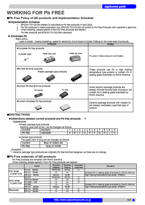
WORKING FOR Pb FREE■Pb Free Policy of QD products and Implementation Schedule●Implementation Schedule1. EPSON TOYOCOM started to manufacture Pb free products in April,2002. 2. For the products in mass production now, EPSON TOYOCOM will switch to Pb Free Products with customer’s approval.3. When ordering, please specify if Non-Pb Free products are desired. Pb free products are EPSON TOYOCOM’s standard. ● Eliminated Pb ‹ Basic policy › “ Lead in solder “ means Soldering- paste for electronic circuit board & Solder Plating on the outer-lead of products.Products Notes•Complete Pb free products.Pb used in these products is eliminated.•Pb free terminal productsThese products use Pb in high meltingtemperature type solders or contain Pb in sealing glass exempted by RoHS directive.•Current Pb free terminal productsSome ceramic package products arealready Pb-free terminal type of product, but contain Pb in sealing glass exempted by RoHS directive.•Current complete Pb free productsCeramic package products with metallic lid are already completely Lead-free type of product.■DISTINCTIONS●Distinctions between current products and Pb free products. *1Appearance•Plastic package type products.Marking (year part lot No.) will be changed as follows.Current Numeric 12345678 9 0 Pb free Alphabet A B C D E F G H J K•Cylinder type productsThe glass color of plug will be changed as follows.Current Blue or Green etc Pb freeGray or White‹ Exception ›*1 Ceramic package type products are originally Pb free terminal designed, so there are no change.■Pb Free materials of QD productsPb Free products are complied with RoHS directive. When ordering,please specify if Non-Pb Free products are desired.ModelTerminalMaterialTerminalPlatingCompleteLead freeRemarksC-xxxx Series Fe-Ni-Co Sn-Cu { FC-xxx Series W Au Contains Pb in sealing glass exempted by RoHS directive.kHz rangeCrystal units MC-xxx Series 42Alloy Sn-Bi High melting temperature type solder. (Pb85%) CA-301 Fe-Ni-Co Sn-Cu { TSX-xxx Series W Au { FA-238V / 238 W Au { FA-365 W Au Contains Pb in sealing glass exempted by RoHS directive.MHz range Crystal units MA-xxx Series 42Alloy Sn-Bi High melting temperature type solder. (Pb85%) NS-xxx Series W Au { ResonatorFS-xxx Series WAu {Plastic package type productsFC SeriesFA-365Cylinder typeMetal Cap typeMetal can typeModelTerminal Material Terminal Plating CompleteLead FreeDefinitionsSG-350 Series 42Alloy Sn-Bi { SG-550 Series 42Alloy Sn-Bi { SG-310 Series W Au { SG-645 Series 42Alloy Sn-Bi High melting temperature type solder. (Pb85%) SG-710 Series W Au { SG-636 / 615 Series 42Alloy Sn-Bi High melting temperature type solder. (Pb85%) SG-51 / 531 Series 42Alloy Sn-Bi High melting temperature type solder. (Pb85%) SG-xxxxLA Series 42Alloy Sn-Bi { SG-xxxxLB Series 42Alloy Sn-Bi { SG-xxxxJC Series 42Alloy Sn-Bi High melting temperature type solder. (Pb85%) SG / HG-xxxxJA Series 42Alloy Sn-Bi High melting temperature type solder. (Pb85%) SG-xxxxJF Series 42Alloy Sn-Bi High melting temperature type solder. (Pb85%) SG-xxxxLC Series 42Alloy Sn-Ag Contains Pb in sealing glass exempted by RoHS directive.SG-xxxxCE Series W Au { SG / HG-xxxxCA Series W Au { TCO-708x Series W Au { TCO-7116H1A W Au { TCO-711A7 / 743 Series Fe-Ni-Co Sn-Cu { TCO-7106X1A / 7107X1A W Au { TCO-391B/C Series Sn-P-Cu Sn-Cu {TCO-393F Cu Au {TCO-3100 Series / 3131 Sn-P-Cu Sn-Cu { XG-xxxxCA / CB Series W Au { EG-xxxxCA Series W Au { MG-5020JE 42Alloy Sn-Ag High melting temperature type solder. (Pb85%) SPXOMG-5100SA 42Alloy Sn-Ag High melting temperature type solder. (Pb85%) TG-xxxxLA / LH Series 42Alloy Sn-Bi { TCO-5860 Series W Au {TCO-5890 Series W Au {TCO-5850 Series W Au { TCXO TCO-5060 / 5160 Series W Au { VG-xxxxCA Series W Au { VG-xxxxJA Series 42Alloy Sn-Bi High melting temperature type solder. (Pb85%) TCO-734A / 735 Series Fe-Ni-Co Sn-Ag-Cu { TCO-7302 Series Fe-Ni-Co Sn-Ag-Cu { TCO-291 Series Sn-P-Cu Sn-Cu { TCO-293 Series Cu Au { TCO-294J Cu Au { TCO-296 Series Cu Au { TCO-2000 / 2100 Series Sn-P-Cu Sn-Cu { TCO-2106 / 2107 Sn-P-Cu Sn-Cu { TCO-2110 Series / 2131 Sn-P-Cu Sn-Cu { TCO-2152 Ag-Pd Au { TCO-726 / 7026 Series W Au { TCO-756 BVX7 / DVX7 Fe-Ni-Co Sn-Cu { TCO-7116 Series W Au { VCXOTCO-7106Z1Z W Au { TCO-6602 TCO-6730TCO-676TCO-6920Fe-Ni(50%)Sn-Cu {OCXO TCO-679 Fe-Ni-Co Sn-Ag-Cu {PLL Module TCM-2021Series Cu Au {RX / RTC-xxxxSA Series 42Alloy Sn-Ag High melting temperature type solder. (Pb85%) RX / RTC-xxxxNB Series Cu Alloy Sn-Ag High melting temperature type solder. (Pb85%) RX / RTC-xxxxJE Series 42Alloy Sn-Ag High melting temperature type solder. (Pb85%)RX-xxxxLC Series 42Alloy Sn-Ag Contains Pb in sealing glass exempted by RoHS directive.RTC-4543SB 42Alloy Sn-Ag High melting temperature type solder. (Pb85%)RTC-7301SF Cu Alloy Sn-Ag High melting temperature type solder. (Pb85%) Real TimeClock Module RTC-62423 / 72423 42Alloy Sn-Bi High melting temperature type solder. (Pb85%)TFx- SeriesW Au { Crystal Filter (MCF)TSx- Series W Au { FF-xxx Series W Au {SAW FilterTQS Series W Au { XV-3500CB W Au { HTS-206 Fe-Ni-Co Sn-Pb High melting temperature type solder. (Pb85%) SensorTSU-10GL/20G/70G/100G Cu Sn { Terminal that joined pressure.■HANDLING PRECAUTIONSWhen using EPSON TOYOCOM products,it is essential to observe the operating conditions specified in their respective specifications or catalogs.■Common points for all products1. Shock resistanceEPSON TOYOCOM’s crystal products are designed to resist physical shocks, but crystal products may be damaged under some conditions, such as dropping from desks or receiving shocks during mounting. Please be sure to re-check the characteristics if product has received any shocks.2. Soldering heat resistanceEPSON TOYOCOM’s crystal products except SMD products use solder having a +180°C to +200°C melting point. Heating up the package more than +150°C may deteriorate the characteristics or damage the products. If the crystal products need to be soldered at temperature of more than +150°C,SMD products are recommended. Using higher temperatures over the following reflow conditions to crystal products, even SMD products, may cause the characteristics to deteriorate. The reflow conditions within following profile is recommended. Always check the soldering temperature and time before mounting these products. Also, please check them again when the mounting conditions are changed. Please contact us for inquiries about heat-resistance if crystal products need to be soldered over the following profile.(1) Cylinder products and DIP productsModel Soldering conditions[ Cylinder ] C-TYPE, C-2-TYPE, C-4-TYPE,HTS-206 +280 °***************.Do not heat the package at more than +150 °C.[ Cylinder ] CA-301[ DIP ] SG-51 / 531, SG-8002DB / DC,RTC-62421 / 72421 / 7301DG TCO-711A7,TCO-743A7/HC7,TCO-756BVX7,DVX7TCO-734A/735/7302 +260 °****************.Do not heat the package at more than +150 °C.(2) SMD products Reflow profile (example)Please make temperature rate as gentle a curve as possible. Also, if the package is cellular, the possibility of cracking is inevitable,so please store it for a short duration and take measures to protect product from dampness when you store it in high humidity. 3. Mounting precautionsShocks by auto mountingShocks caused by auto mounting and vacuuming may deteriorate the characteristics and affect the products. Please set the mounting conditions to minimize the shocks as much as possible, and be sure that there is no affect on the characteristics before mounting. Please review the conditions after the conditions are changed. Also please be sure that crystal products don’t hit machines or other electric boards, etc. before or after mounting.(1) a) Ceramic package products and SON productsBending the board after soldering ceramic package products and SON products (MC-146,RTC-****NB,RX-****NB) may cause peeling off portions of soldering or package cracks by mechanical stress. Particularly, in the case of cutting boards after soldering these products, please be sure to layout the crystal on a less stressed location and use less stressed cutting method.b) Ceramic package productsIn the case of soldering ceramic package products on a different expansion-coefficient board (ex. Epoxy Glass),soldering crack at the foot pattern would be expected under repeated temperature changes for a long period. Under these conditions, be sure to。
爱普生晶振RA8900CE实时时钟模块(I

DIVIDER
POWER CONTROLLER
INTERRUPTS CONTROLLER
FOUT CONTROLLER
BUS INTERFACE CIRCUIT
CLOCK and
CALENDR
TIMER REGISTER
ALARM REGISTER
CONTROL R EG ISTER
and SYSTEM
Min.
Typ.
Max.
VDD
2.5
3.0
5.5
V
VTEM
2.0
3.0
5.5
V
VCLK
1.6
3.0
5.5
V
TOPR UA
∆ f / f UB UC
-40
+25
+85
Ta = -40 ºC ~ +85 ºC
±3.4 ∗1
Ta = -40 ºC ~ +85 ºC Ta = -30 ºC ~ +70 ºC
CONTROL LER
• •UA •UB •UC
± 3.4 x 10⁻⁶ / -40 ºC ~ +85 ºC 商 ± 5.0 x 10⁻⁶ / -40 ºC ~ +85 ºC 商 ± 5.0 x 10⁻⁶ / -30 ºC ~ +70 ºC 商
9
器
13
器
13
器
• 32.768 kHz • FOUT •
Frequency temperature characteristics
10
5 32.768 kHz DTCXO
0
-5
-10
-15 Tuning fork X'tal
爱普生(EPSON)实时时钟模块RX-4581NB规格书
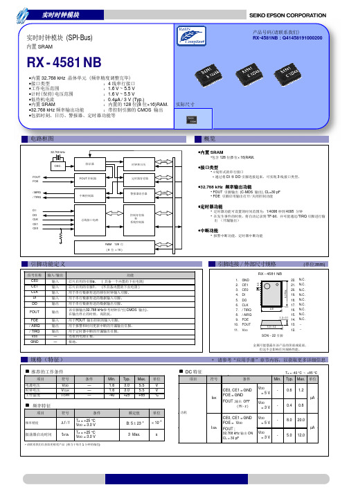
•
•4
∗
DI DO
3
•32Hale Waihona Puke 768 kHz• FOUT
• FOE
(C-MOS 属
), CL=30 pF
•
•
•
1/4096 TF-bit
4095 /TIRQ
•
•
属
1. GND 2. CE1 3. CE0 4. DI 5. DO 6. CLK 7. / TIRQ 8. / AIRQ 9. FOE 10. FOUT 11. VDD
32.768 kHz
FOUT FOE
/ AIRQ / TIRQ
OSC.
DI DO CLK CE1 CE0
FOUT
RAM 128 ( 8 × 16 )
属
CE0 CE1 CLK DI DO
FOUT
FOE
/ AIRQ
/ TIRQ
VDD
-
GND
-
0( 1(
32.768 kHz FOUT
) )
( CMOS )
1.太空设备(人造卫星、火箭等) 2.运输车辆机器控制装置(汽车、飞机、火车、船舶等) 3.用于维持生命的医疗器械 4.海底中转设备 5.发电站控制机器 6.防灾防盗装置 7.交通设备 8.其他,用于与 1~7 具有同等可靠性的用途。
本材料中记载的品牌名称或产品名称是其所有人的商标或注册商标。
Seiko Epson Corporation
DC
Ta = -40 °C ~ +85 °C
Min. Typ. Max.
CE0, CE1 = GND FOE = GND
VDD =5V
-
EPSON 实时时钟芯片RX-8010SJ Application Manual介绍
----------------------------------------------------------------------------------------------------------------------------------------
1.
概述 这是一款内置 32.768k 晶体单元的实时时钟模块。除了具有计时、日历的基本功能以外, 还具有定时中断、固定周期中断、频率缺失检测、频率输出、用户 RAM 等功能。8 Pin 的 SOP 封装使之适合于多种小型化电子设备的应用。 2. 结构框图
RX-8010SJ 12.3 寄存器介绍及使用
12.3.1 时钟日历寄存器 在通讯开始后,时钟和日历的数据会保持不变,等到通讯结束后会自动更新。因此推荐 使用连续访问的方式一次性读取时间数据。 设置举例: 88 年 2 月 29 日 星期天 17:39:45
1) 2) 3)
[SEC],[MIN] 寄存器使用 60 进制的 BCD 码,数据范围 00 – 59 [HOUR]寄存器使用 24 进制 BCD 码,时间采用 24 小时格式。 [WEEK]寄存器用单独的一位来表示对应的星期。见下表:
RX-8010SJ
3. 引脚定义
3.1 引脚功能描述
4. 外观尺寸
RX-8010SJ
5. 推荐操作条件
6. 频率特性
RX-8010SJ
7. 电器特性 (直流)
8. IIC 总线时序特性
RX-8010SJ
9.使用中特别注意事项 9.1 上电 9.1.1 供电电压特性 * tR1 作为上电复位的限制条件,当不能满足这个条件时,不能正常实现上电复位。 必须通过软件对系统进行初始化设置。 *在短时间内电源频繁 ON/OFF 变化,会导致上电复位不可靠。在掉电以后,要保持 VDD= GND 这种状态 60 s 以上的时间以保证上电复位的可靠性。如果不能满足这个条 件,请通过软件的初始化来设置系统。
Epson America, Inc. GPS Running Watch用户指南说明书

© 2017 Epson America, Inc., 5/17 CPD-54145Printed in ChinaGPS Running WatchNoticesSafety SymbolsThe following symbols are used in this guide to indicate possible dangerous operations or handling. Make sure youunderstand these warnings before using the product.• Make sure you read the manuals (this Notices sheet,the Quick Start Guide and the online User’s Guide ) first to use this product safely. This product is equipped with Bluetooth® Smart technology as a built-in wireless function. See the section “Notes on Electromagnetic Waves” in the online User’s Guide for more information.• The product may malfunction, or an accident may occur if it is handled incorrectly.• Keep the manuals handy to help you resolve any problems.• When taking this product out of the country of purchase, check the laws and regulations in the destination country before you travel.• This product is not a medical device. Use this product to track physical exercise.17Declaration of ConformityAccording to 47CFR, Part 2 and 15, Class B PersonalComputers and Peripherals; and/or CPU Boards and Power Supplies used with Class B Personal Computers:We: Epson America, Inc.Located at: 3840 Kilroy Airport Way, MS 3-13, Long Beach, CA 90806Telephone: (562) 981-3840Declare under sole responsibility that the product identified herein, complies with 47CFR Part 2 and 15 of the FCC rules as a Class B digital device. Each product marketed, is identical to the representative unit tested and found to be compliant with the standards. Records maintained continue to reflect the equipment being produced can be expected to be within the variation accepted, due to quantity production and testing on a statistical basis as required by 47CFR §2.909. Operation is subject to the following two conditions: (1) this device may not cause harmful interference, and (2) this device must accept any interference received, including interference that may cause undesired operation.Trade Name: EpsonType of Product: GPS Running Watch Model: J-17Marketing Name: ProSense 17FCC/IC NoticesFCC ID: BKMAP008CAN ICES-3(B)/NMB-3(B)IC: 1052F-AP008This transmitter must not be co-located or operated in conjunction with any other antenna or transmitter.This device complies with Part 15 of FCC Rules and Industry Canada licence-exempt RSS standard(s). Operation is subject to the following two conditions: (1) this device may not cause interference, and(2) this device must accept any interference, including interference that may cause undesired operation of this device.Caution: Changes or modifications not expresslyapproved by the party responsible for compliance could void the user’s authority to operate the equipment.This equipment complies with FCC/IC radiation exposure limits set forth for an uncontrolled environment and meets the FCC radio frequency (RF) Exposure Guidelines and RSS-102 of the IC radio frequency (RF) Exposure rules. This equipment has very low levels of RF energy that are deemed to comply without testing of specific absorption ratio (SAR).Note: This equipment has been tested and found tocomply with the limits for a Class B digital device, pursuant to part 15 of the FCC Rules. These limits are designed to provide reasonable protection against harmfulinterference in a residential installation. This equipment generates, uses and can radiate radio frequency energy and, if not installed and used in accordance with the instructions, may cause harmful interference to radio communications. However, there is no guarantee that interference will not occur in a particular installation. Ifthis equipment does cause harmful interference to radio or television reception, which can be determined by turning the equipment off and on, the user is encouraged to try to correct the interference by one or more of the following measures:• Reorient or relocate the receiving antenna.• Increase the separation between the equipment and receiver.• C onnect the equipment into an outlet on a circuit different from that to which the receiver is connected.• Consult the dealer or an experienced radio/TV technician for help.Epson America, Inc., 3840 Kilroy Airport Way, Long Beach, CA 90806, Tel: (562) 981-3840.One-Year Limited WarrantyWhat Is Covered: Epson America, Inc. (“Epson”) warrantsto the original retail purchaser of the Epson product enclosed with this limited warranty statement that the product, if purchased new and operated in the United States, Canada, or Puerto Rico will be free from defects in workmanship and materials for a period of One (1) year from the date of original purchase. For warranty service, you must provide proof of the date of original purchase. What Epson Will Do To Correct Problems: If your product requires service during the limited warranty period, please call the Epson Connection SM at the number on the bottom of this statement and be prepared to provide the model, serial number, and date of original purchase. An Epson service technician will provide telephone diagnostics to determine whether the product requires service. If the product requires service, Epson will, at its option, repair or replace the defective unit, without charge for parts or labor. When Epson authorizes an exchange for thedefective unit, Epson will ship a replacement product toyou, freight prepaid, so long as you use an address in theUnited States, Canada, or Puerto Rico. You are responsiblefor securely packaging the defective unit and returningit to Epson within Five (5) working days of receipt ofthe replacement. Epson requires a debit or a credit cardnumber to secure the cost of the replacement product inthe event that you fail to return the defective one. Whenwarranty service involves the exchange of the product orof a part, the item replaced becomes Epson property. Theexchanged product or part may be new or equivalent tonew in reliability and performance, and at Epson’s option,the replacement may be another model of like kindand quality. Exchange or replacement products or partsassume the remaining warranty period of the productcovered by this limited warranty.What This Warranty Does Not Cover: This warranty coversonly normal use in the United States, Canada or PuertoRico. This warranty does not cover normal wear and tear;including nicks and scratches, and battery life, unlessthe damage was caused by a manufacturing defect inmaterials and workmanship. This warranty does not coverdamage caused by parts or services not manufactured,distributed, or certified by Epson nor any lossesattributable to the loss or restoration of customer data.Epson does not warrant that the operation of the productwill be error-free, that we will correct errors, or your useof the product and software will be uninterrupted. Thiswarranty does not cover misuse caused by high impactwear or damage caused by exposure to water as specifiedin the product user manual. This warranty does not coverskin irritation arising from wear. See the ProSense onlineUser’s Guide and Quick Start Guide for wear and careinstructions. This warranty is not transferable. Software forthis product is not covered under this warranty. See theEpson View website for software warranties. Epson is notresponsible for warranty service should the Epson labelor logo or the rating label or serial number be removed.Epson is not responsible for warranty service should theproduct fail to be properly maintained or fail to functionproperly as a result of misuse, abuse, improper installation,neglect, improper shipping, damage caused by disasterssuch as fire, flood, and lightning, improper electricalcurrent, software problems, interaction with non-Epsonproducts, or service other than by Epson or an EpsonAuthorized Servicer. Postage, insurance, or shipping costsincurred in presenting your Epson product for warrantyservice are your responsibility. If a claimed defect cannotbe identified or reproduced in service, you will be heldresponsible for costs incurred.DISCLAIMER OF OTHER WARRANTIES: THE WARRANTYAND REMEDY PROVIDED ABOVE ARE EXCLUSIVE AND INLIEU OF ALL OTHER EXPRESS OR IMPLIED WARRANTIESINCLUDING, BUT NOT LIMITED TO, THE IMPLIEDWARRANTIES OF MERCHANTABILITY, NONINFRINGEMENTOR FITNESS FOR A PARTICULAR PURPOSE. SOME LAWS DONOT ALLOW THE EXCLUSION OF IMPLIED WARRANTIES.IF THESE LAWS APPLY, THEN ALL EXPRESS AND IMPLIEDWARRANTIES ARE LIMITED TO THE WARRANTY PERIODIDENTIFIED ABOVE. UNLESS STATED HEREIN, ANYSTATEMENTS OR REPRESENTATIONS MADE BY ANY OTHERPERSON OR FIRM ARE VOID.EXCLUSION OF DAMAGES; EPSON’S MAXIMUM LIABILITY:IN NO EVENT SHALL EPSON OR ITS AFFILIATES BE LIABLEFOR ANY SPECIAL, INCIDENTAL, OR CONSEQUENTIALDAMAGES OR ANY LOST PROFITS RESULTING FROMTHE USE OR INABILITY TO USE THE EPSON PRODUCT,WHETHER RESULTING FROM BREACH OF WARRANTY ORANY OTHER LEGAL THEORY. IN NO EVENT SHALL EPSONOR ITS AFFILIATES BE LIABLE FOR DAMAGES OF ANY KINDIN EXCESS OF THE ORIGINAL RETAIL PURCHASE PRICE OFTHE PRODUCT.Arbitration, Governing Laws: Any dispute, claim orcontroversy arising out of or relating to this warrantyshall be determined by arbitration in Los Angeles County,California before a single arbitrator. The arbitration shallbe administered by JAMS pursuant to its ComprehensiveArbitration Rules and Procedures. Judgment on theaward may be entered in any court having jurisdiction.Any action must be brought within three months of theexpiration of the warranty. This clause shall not precludeparties from seeking provisional remedies in aid ofarbitration from a court of appropriate jurisdiction. Thiswarranty shall be construed in accordance with the lawsof the State of California, except this arbitration clausewhich shall be construed in accordance with the FederalArbitration Act.Other Rights You May Have: This warranty gives you specificlegal rights, and you may also have other rights whichvary from jurisdiction to jurisdiction. Some jurisdictionsdo not allow limitations on how long an implied warrantylasts, or allow the exclusion or limitation of incidentalor consequential damages, so the above limitations orexclusions may not apply to you.In Canada, warranties include both warranties andconditions.To find the Epson Authorized Reseller nearest you, pleasevisit in the U.S. or www.epson.ca inCanada.For product support, please visit/support in the U.S. orwww.epson.ca/support in Canada.To contact the Epson Connection, please call(800) 241-5789 or (562) 276-4394 in the U.S. and(905) 709-3839 in Canada or write to Epson America, Inc.,P.O. Box 93012, Long Beach, CA 90809-3012.。
爱普生晶振最小包装数量_标准包装规格
L L L L L L L L L L L L L L L L L L L L L L L L L L L
【南京南山:EPSON晶振代理证书编号14013】
●SAW 谐振器
型号 FS-335 FS-555 FS-585 NS-21R NS-32R 数量 (件/卷筒) 4000 4000 4000 3000 4000 1000 3000 3000 3000 1000 1000 2000 1000 2000 2000 2000 1000 1000 1000 1000 1000 1000 1000 1000 1000 1000 1000 1000 1000 1000 1000 1000 1000 1000 2000 1000 1000 1000 2000 1000 2000 3000 1000 2000 1000 1000 2000 1000 1000 1000 1000 2000 1000 1000 1000 1000 12000 2000 2000 12000 1000 1000 1000 1000 a Φ330 Φ330 Φ330 Φ180 Φ330 Φ254 Φ180 Φ180 Φ180 Φ330 Φ254 Φ180 Φ330 Φ180 Φ180 Φ180 Φ180 Φ330 Φ330 Φ254 Φ254 Φ180 Φ254 Φ180 Φ180 Φ180 Φ180 Φ180 Φ180 Φ180 Φ180 Φ180 Φ180 Φ254 Φ180 Φ330 Φ330 Φ254 Φ254 Φ254 Φ180 Φ180 Φ254 Φ254 Φ254 Φ330 Φ254 Φ330 Φ330 Φ254 Φ180 Φ180 Φ254 Φ180 Φ180 Φ180 Φ330 Φ180 Φ180 Φ330 Φ180 Φ180 Φ254 Φ180 卷筒尺寸 b Φ80 or Φ100 Φ80 or Φ100 Φ80 or Φ100 Φ60 Φ80 or Φ100 Φ100 Φ60 Φ60 Φ60 Φ80 or Φ100 Φ100 Φ60 Φ80 or Φ100 Φ60 Φ60 Φ60 Φ60 Φ80 or Φ100 Φ80 or Φ100 Φ100 Φ100 Φ60 Φ100 Φ60 Φ60 Φ60 Φ60 Φ60 Φ60 Φ60 Φ60 Φ60 Φ60 Φ100 Φ60 Φ80 or Φ100 Φ80 or Φ100 Φ100 Φ100 Φ100 Φ60 Φ60 Φ100 Φ100 Φ100 Φ80 or Φ100 Φ100 Φ80 Φ80 Φ100 Φ60 Φ60 Φ100 Φ60 Φ60 Φ60 Φ100 Φ60 Φ60 Φ100 Φ60 Φ60 Φ100 Φ60 W 13.5 13.5 13.5 9.0 13.5 17.5 9 9 13 17.5 17.5 13 17.5 13 9 9 13 25.5 17.5 17.5 17.5 17 17.5 13 13 13 17 17 17 17 13 17 13 17.5 9 25.5 17.5 17.5 13.4 17.5 9 9 17.5 13.4 17.5 17.5 13.4 25.5 25.5 17.5 13 9 17.5 17 13 17 9.4 9 9 9.4 13 13 17.5 17 A 8.0 8.0 8.0 4.0 8.0 8 4 4 4 8 8 4 8 4 4 4 8 12 8 8 8 8 8 8 8 8 8 8 8 8 8 8 8 8 4 12 8 8 8 8 4 4 8 8 8 8 8 12 12 8 8 4 8 8 8 8 4 4 4 4 8 8 8 8 职业磁带尺寸 B C 7.25 12.0 7.25 12.0 7.25 12.0 5.25 8.0 7.25 12.0 9.25 5.25 5.25 7.25 9.25 9.25 7.25 9.25 7.25 5.25 5.25 7.25 13.25 9.25 9.25 9.25 9.25 9.25 7.25 7.25 7.25 9.25 9.25 9.25 9.25 7.25 9.25 7.25 9.25 5.25 13.25 9.25 9.25 7.5 9.25 5.25 5.25 9.25 7.5 9.25 9.25 7.5 13.25 13.25 9.25 7.25 5.25 9.25 9.25 7.25 9.25 5.25 5.25 5.25 5.25 7.25 7.25 9.25 9.25 16 8 8 12 16 16 12 16 12 8 8 12 24 16 16 16 16 16 12 12 12 16 16 16 16 12 16 12 16 8 24 16 16 12 16 8 8 16 12 16 16 12 24 24 16 12 8 16 16 12 16 8 8 8 8 12 12 16 16
EPSON-LS系列手册(中文版)

EPSON-LS系列手册(中文版)这个手册旨在提供对EPSON-LS系列的总体描述和目的。
它将提供针对该系列的详细信息,包括产品规格、设置指南和操作步骤等。
无论是新手还是有经验的用户,都可以通过本手册来了解如何正确使用EPSON-LS系列产品,并充分利用其功能和特点。
本手册的目标是以简洁、清晰的语言提供信息,帮助用户快速上手并解决常见问题。
通过本手册,用户将能够全面了解EPSON-LS系列产品,并正确设置和操作其功能。
我们建议用户在使用EPSON-LS系列产品之前仔细阅读本手册,以确保能够获得最佳的使用体验。
请注意,本手册中的所有内容均基于最新可确认的信息。
在引用任何内容之前,请确保其准确性和可靠性。
本手册主要介绍EPSON-LS系列的主要特点和功能。
高精度定位:EPSON-LS系列手册采用先进的定位技术,可以实现高精度的定位和控制,确保产品的准确性和稳定性。
多功能操作:EPSON-LS系列手册提供多种操作模式,包括自动模式、手动模式和远程控制模式,能够适应不同的使用需求。
强大的数据处理能力:EPSON-LS系列手册配备了先进的数据处理功能,可以实时处理大量的数据,提供精确的结果和分析。
灵活的配置选项:EPSON-LS系列手册支持多种配置选项,可以根据用户的需求进行灵活的配置和定制。
易于使用和维护:EPSON-LS系列手册拥有直观友好的用户界面和简单易懂的操作流程,方便用户使用和维护。
以上是EPSON-LS系列手册的主要特点和功能,希望能够帮助用户更好地了解和使用该产品。
本手册将为您提供EPSON-LS系列设备的详细使用指南,包括操作步骤和注意事项。
请按照以下指南使用设备:准备工作:确保设备的电源已连接并正常工作。
将设备与计算机或其他外部设备正确连接。
操作步骤:打开EPSON-LS系列手册中提供的软件或应用程序。
在菜单中选择所需的功能或操作。
根据提示或手册中的说明执行相应的操作步骤。
注意事项:请务必仔细阅读并理解手册中的操作说明,遵循正确的操作步骤。
RX8111CE模块说明书

RX8111CE 封装转换模块说明文件特性:将RTC (RX8111CE )和周边器件设计到一个合适大小的PCBA 上,完成最小系统设计。
该模块的特性和RX8111CE 特性相同,具体参考RX8111CE 使用手册。
https:///en/products/rtc/rx8111ce.html-内置32.768k 晶体-宽电压支持:1.6V ~ 5.5V -接口类型:IIC -低备份电流:100nA Typ./3V-8级时间戳功能-丰富中断功能应用:-工业仪表-各种计时设备-手持低功耗设备等==================================================================================模块上RX8111CE引脚定义及封装尺寸:(正面图)(反面图)EPS0N RTC 尺寸:10.25±0.3*7.3±0.2*2.0±0.2mm转换模块电路设计:不同功能模式的阻容配置:模式:预装器件(除RX-8111CE ):备注:兼容RX-8025SA 模式C1,C2,C3,R1,R4RX8111CE:VDD,VBAT,VIO 接一起RX8111CE 评估模式C1,C2,C3,R1,R2,R3,R5评估外接电池(评估默认接法)C1,C2,C3,R2,R3,R5,R6IIC 总线电平电压不同,vio 测试模块引脚定义:模块引脚功能定义:1.V_Bat2.SCL3.FOUT4.NC5.NC6.VDD7.NC 14.V_Io 13.SDA 12.NC 11.GND 10./INT 9.NC 8.EVIN引脚名:I/O功能:1.V_Bat--备份电源接口,可接电池(可充电),电容2.SCL Input IIC串行时钟输入硬件3.FOUT Output频率输出引脚(CMOS)6.VDD--电源引脚8.EVIN Input外部触发输入,用于时间戳触发。
爱普生晶振RX8900CE实时时钟模块(I
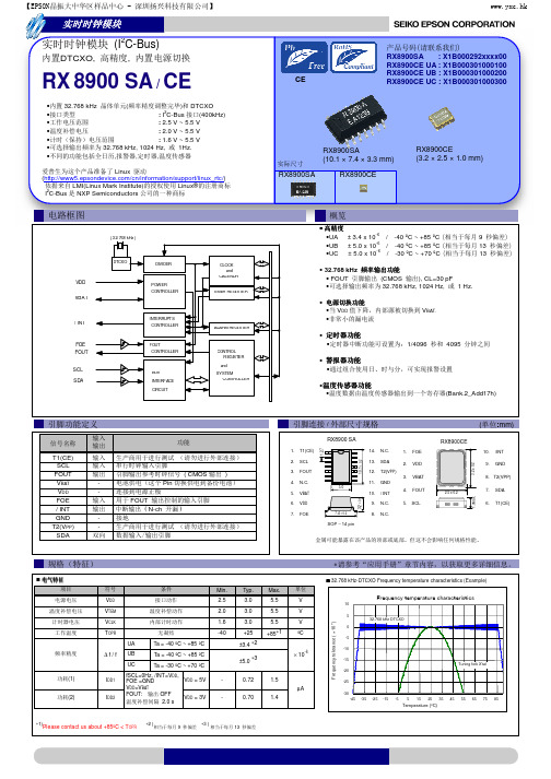
本材料中记载的品牌名称或产品名称是其所有人的商标或注册商标。
Seiko Epson Corporation
-
T2(VPP)
-
SDA
( CMOS
)
Pin
பைடு நூலகம்
FOUT
( N-ch
)
属
1. T1(CE) 2. SCL 3. FOUT 4. N.C. 5. VBAT 6. VDD 7. FOE
1.2 7
/
RX8900 SA
5.0 7.4 ± 0.2
SOP − 14 pin
3.2 ± 0.1
10.1 ± 0.2
14. N.C.
9
器
13
器
13
器
• 32.768 kHz • FOUT •
(CMOS ), CL=30 pF 32.768 kHz, 1024 Hz, 1 Hz.
• • VDD •
VBAT.
•
•
1/4096
4095
• •
•
•
(Bank.2_Add17h)
T1(CE)
SCL
FOUT
VBAT
-
VDD
-
FOE
/ INT
GND
•
,
,
,
Linux
(/cn/information/support/linux_rtc/)
LMI(Linux Mark Institute) I2C-Bus NXP Semiconductors
- 1、下载文档前请自行甄别文档内容的完整性,平台不提供额外的编辑、内容补充、找答案等附加服务。
- 2、"仅部分预览"的文档,不可在线预览部分如存在完整性等问题,可反馈申请退款(可完整预览的文档不适用该条件!)。
- 3、如文档侵犯您的权益,请联系客服反馈,我们会尽快为您处理(人工客服工作时间:9:00-18:30)。
电路框图
外部尺寸规格/引脚连接(单位:mm)
规格说明(特征)*请参考“应用手册”章节内容,以获取更多详细信息。
RTC-7301SF
推进环境管理体系 符合国际标准
在环境管理体系的运行方面,使用ISO14001国际环境标准,通过“计划-实施-检查-验证(PDCA)的循环来实现持续改进。
公司位于日本和海外的主要制造基地已取得了ISO14001资格认证。
追求高品质
Seiko Epson 为了向顾客提供高品质、卓越信赖性的产品、服务,迅速着手通过ISO 9000系列资格认证的工作,其日本和海外工厂也在通过ISO 9001认证。
同时,也在通过大型汽车制造厂商要求规格的ISO/TS 16949认证。
关于在目录内使用的记号
●无铅。
●符合欧盟RoHS 指令。
欧盟RoHS 指令免检的含铅产品。
(密封玻璃、高温熔化性焊料或其他材料中包含铅。
)
●为汽车方面的应用,如汽车多媒体、车身电子、遥控无钥门锁等。
●为汽车行驶安全方面的应用(引擎控制单元、气囊、电子稳定程序控制系统)。
注意事项
·本材料如有变更,恕不另行通知。
量产设计时请确认最新信息。
·未经Seiko Epson 公司书面授权,禁止以任何形式或任何方式复制或者发布本材料中任何部分的信息内容。
·本材料中的书面信息、应用电路、编程、使用等内容仅供参考。
Seiko Epson 公司对第三方专利或版权的侵权行为不负有任何责任。
本材料未对任何专利或知识版权的许可权进行授权。
·本材料中规格表中的数值大小通过数值线上的大小关系表示。
·当出口此材料中描述的产品或技术时,你应该遵守相应的出口管制法律和法规,并按照这些法律和法规的要求执行。
请不要将产品(以及任何情况下提供任何的技术信息)用于开发或制造大规模杀伤性武器或其他军事用途。
还要求,不要将产品提供给任何将产品用于此类违禁用途的第三方。
·此类产品是基于在一般电子机械内使用而设计开发的,如将产品应用于需要极高可靠性的特定用途,必须实现得到弊公司的事前许可。
若无许可弊公司将不负任何责任。
1.太空设备(人造卫星、火箭等)
2.运输车辆机器控制装置(汽车、飞机、火车、船舶等)
3.用于维持生命的医疗器械
4.海底中转设备
5.发电站控制机器
6.防灾防盗装置
7.交通设备
8.其他,用于与1~7具有同等可靠性的用途。
本材料中记载的品牌名称或产品名称是其所有人的商标或注册商标。
Seiko Epson Corporation
ISO 14000 是国际标准化组织于1996年在全球化变暖、臭氧层破坏、以及全球毁林等环境问题日益严重的背景下提出的环境管理国际标准。
ISO/TS16949是一项国际标准,是在ISO9001的基础上增加了对汽车工业的特殊要求部分。