标准CMOS工艺集成肖特基二极管设计与实现_英文文献和翻译
标准CMOS工艺集成肖特基二极管设计与实现
标准CMOS工艺集成肖特基二极管设计与实现
0 引言
随着射频无线通信事业的发展和移动通讯技术的进步,射频微波器件的性能与速度成为人们关注的重点,市场对其的需求也日益增多。
目前,CMOS 工艺是数字集成电路设计的主要工艺选择,对于模拟与射频集成电路来说,选择的途径有多种,例如Si双极工艺、GaAs工艺、CMOS工艺等,在设计中,性能、价格是主要的参考依据。
除此以外,工艺的成熟度及集成度也是重要的考虑范畴。
1.CMOS工艺技术
近几十年,因为CMOS技术的发展,也使得在制造射频集成电路时,采用CMOS技术得以实现。
但是,因为CMOS制造工艺通常是以数字电路作为导向。
面向数字电路设计的CMOS首先由芯片代工厂研发出来,注重功率耗散与时速。
在数字CMOS工艺快速发展成熟以后,在其基础上,通过修改制程与添加掩膜层实现信号的混合及模拟射频CMOS工艺。
传统CMOS工艺包含BJTs、MOSFETs以及各种电阻,如扩散电阻、多晶硅电阻及N阱电阻。
但是,对于CMOS工艺而言,还应该涵盖各种高频无源器件,例如变容二极管、MIM电容、高Q值电杆及变压器等。
同样,作为肖特基二极管来说,也是CMOS工艺技术的重要环节。
例如,需要额外高能离子注入形成深注入N阱降低程度耦合与噪声系数。
需要注意的是,尽管射频CMOS工艺是基于数字CMOS工艺而来,但其不仅仅是添加几层掩膜来实现高频无源器件,对于器件的性能而言,射频工艺与数字工艺的优化目标是不同的,在进行改进的时候,也有可能与传统的。
肖特基二极管的结构及工作原理
肖特基二极管的结构及工作原理A Schottky diode is a two-terminal metal-semiconductor device, which is composed of a metal that is in close contact with a semiconductor material. 肖特基二极管是一种两端金属-半导体器件,由金属和半导体材料密切接触而组成。
It is named after the German physicist Walter H. Schottky. 它以德国物理学家瓦尔特·肖特基的名字命名。
The structure of a Schottky diode is different from that of a standard P-N junction diode. 肖特基二极管的结构不同于标准的P-N结二极管。
Instead of a P-N junction, it has a metal-semiconductor junction. 它不是P-N结,而是金属-半导体结。
This metal-semiconductor junction allows the Schottky diode to have a much faster switching speed and lower forward voltage drop compared to a standard diode. 这种金属-半导体结使得肖特基二极管的开关速度更快,正向电压降低,相对于标准二极管而言。
The working principle of a Schottky diode is based on the Schottky barrier. 肖特基二极管的工作原理是基于肖特基势垒。
When a metal comes into contact with a semiconductor material, it forms a barrier known as the Schottky barrier. 当金属与半导体材料接触时,形成一个称为肖特基势垒的障碍。
一种改进太阳能计算器芯片二极管稳压电路设计

一种改进太阳能计算器芯片二极管稳压电路设计张立荣【摘要】For solar energy calculator, the voltage regulator circuit is composed by three PN junction diodes in series. The design may cause some issue:because of the higher Vf for voltage regulator circuit, the voltage of solar energy battery is too higher to arouse voltage can not release in time when sunlight is strong. These issue will lead to calculator can not work well. This paper improve the design of diode voltage regulator circuit. One PN junction diode be changed to shottky diode by change P+mask. So the Vf get more reasonable range than ever. What is more, the impact is researched on thickness of Ti layer and temperature. Finally, it show that this improvement fit our requirement.% 对于太阳能计算器,稳压电路的设计是串联三个PN结二极管以达到稳压目的。
这种设计会出现以下问题:当外部光线太强时,太阳能电池板的供电电压较高,而稳压电路由于正向饱和压降过高,不能及时将高电压释放掉,会造成计算器不能正常工作。
肖特基(Schottky)二极管
肖特基(Schottky)二极管肖特基(Schottky)二极管,又称肖特基势垒二极管(简称 SBD),它属一种低功耗、超高速半导体器件。
最显著的特点为反向恢复时间极短(可以小到几纳秒),正向导通压降仅0.4V左右。
其多用作高频、低压、大电流整流二极管、续流二极管、保护二极管,也有用在微波通信等电路中作整流二极管、小信号检波二极管使用。
在通信电源、变频器等中比较常见。
一个典型的应用,是在双极型晶体管 BJT 的开关电路里面, 通过在 BJT 上连接 Shockley 二极管来箝位,使得晶体管在导通状态时其实处于很接近截止状态,从而提高晶体管的开关速度。
这种方法是 74LS,74ALS,74AS 等典型数字 IC 的 TTL内部电路中使用的技术。
肖特基(Schottky)二极管的最大特点是正向压降 VF 比较小。
在同样电流的情况下,它的正向压降要小许多。
另外它的恢复时间短。
它也有一些缺点:耐压比较低,漏电流稍大些。
选用时要全面考虑。
三、晶体二极管晶体二极管在电路中常用“D”加数字表示,如: D5表示编号为5的二极管。
1、作用:二极管的主要特性是单向导电性,也就是在正向电压的作用下,导通电阻很小;而在反向电压作用下导通电阻极大或无穷大。
正因为二极管具有上述特性,无绳电话机中常把它用在整流、隔离、稳压、极性保护、编码控制、调频调制和静噪等电路中。
电话机里使用的晶体二极管按作用可分为:整流二极管(如1N4004)、隔离二极管(如1N4148)、肖特基二极管(如BAT85)、发光二极管、稳压二极管等。
2、识别方法:二极管的识别很简单,小功率二极管的N极(负极),在二极管外表大多采用一种色圈标出来,有些二极管也用二极管专用符号来表示P极(正极)或N极(负极),也有采用符号标志为“P”、“N”来确定二极管极性的。
发光二极管的正负极可从引脚长短来识别,长脚为正,短脚为负。
3、测试注意事项:用数字式万用表去测二极管时,红表笔接二极管的正极,黑表笔接二极管的负极,此时测得的阻值才是二极管的正向导通阻值,这与指针式万用表的表笔接法刚好相反。
Schottky Barrier Diode
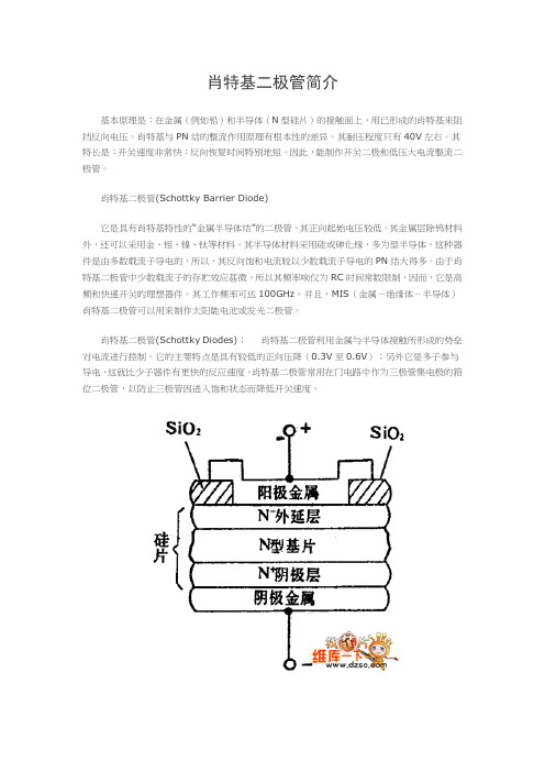
肖特基二极管简介基本原理是:在金属(例如铅)和半导体(N型硅片)的接触面上,用已形成的肖特基来阻挡反向电压。
肖特基与PN结的整流作用原理有根本性的差异。
其耐压程度只有40V左右。
其特长是:开关速度非常快:反向恢复时间特别地短。
因此,能制作开关二极和低压大电流整流二极管。
肖特基二极管(Schottky Barrier Diode)它是具有肖特基特性的“金属半导体结”的二极管。
其正向起始电压较低。
其金属层除钨材料外,还可以采用金、钼、镍、钛等材料。
其半导体材料采用硅或砷化镓,多为型半导体。
这种器件是由多数载流子导电的,所以,其反向饱和电流较以少数载流子导电的PN结大得多。
由于肖特基二极管中少数载流子的存贮效应甚微,所以其频率响仅为RC时间常数限制,因而,它是高频和快速开关的理想器件。
其工作频率可达100GHz。
并且,MIS(金属-绝缘体-半导体)肖特基二极管可以用来制作太阳能电池或发光二极管。
肖特基二极管(Schottky Diodes):肖特基二极管利用金属与半导体接触所形成的势垒对电流进行控制。
它的主要特点是具有较低的正向压降(0.3V至0.6V);另外它是多子参与导电,这就比少子器件有更快的反应速度。
肖特基二极管常用在门电路中作为三极管集电极的箝位二极管,以防止三极管因进入饱和状态而降低开关速度。
肖特基势垒二极管SBD(Schottky Barrier Diode,简称肖特基二极管)是近年来间世的低功耗、大电流、超高速半导体器件。
其反向恢复时间极短(可以小到几纳秒),正向导通压降仅0.4V左右,而整流电流却可达到几千安培。
这些优良特性是快恢复二极管所无法比拟的。
中、小功率肖特基整流二极管大多采用封装形式。
1.结构原理综上所述,肖特基整流管的结构原理与PN结整流管有很大的区别通常将PN结整流管称作结整流管,而把金属-半导管整流管叫作肖特基整流管,近年来,采用硅平面工艺制造的铝硅肖特基二极管也已问世,这不仅可节省贵金属,大幅度降低成本,还改善了参数的一致性。
关于肖特基二极管的文献介绍
关于肖特基二极管的文献介绍[1]Vishal P. Trivedi, Jay P. John, Kun-Hin To, and W. Margaret Huang. A Novel Integration ofSi Schottky Diode for mmWave CMOS, Low-Power SoCs, and More [J]. IEEE Electron Device Letters, VOL. 32, NO. 3, March 2011, 258-260.[2]S. Sankaran and K. O. Kenneth, “S chottky barrier diodes for millimeter wave detection in afoundry CMOS process,” IEEE Electron Dev. Lett., vol. 26, no. 7, pp. 492–494, Jul. 2005. [3]R. M. Rassel, J. B. Johnson, B. A. Orner, S. K. Reynolds, M. E. Dahlstrom, J. S. Rascoe, A. J.Joseph, B. P. Gaucher, J. S. Dunn, and S. A. St. Onge, “Schottky barrier diodes for millimeter wave SiGe BiCMOS Applications,” in Proc. IEEE BCTM, 2006, pp. 255–258. [4]U. R. Pferiffer, C. Mishra, R. M. Rassel, S. Pinkett, and S. K. Reynolds, “Schottky barrierdiode circuits in silicon for future millimeter-wave and terahertz applications,” IEEE Trans.Microw. Theory Tech., vol. 56, no. 2, pp. 364–371, Feb. 2008.[5]M. K. Matters-Kammerer, L. Tripodi, R. van Langevelde, L. Cumana, and R. H. Jansen, “RFcharacterization of Schottky diodes in 65-nm CMOS,” IEEE Trans. Electron Devices, vol. 57, no. 5, pp. 1063–1068, May 2010.[6]Xi-Ning Wang ; Bin Zhu ; Jian-Kun Su ; Ting-Huang Lee ; Li-wu Yang, A novel model foran integrated rf CMOS schottky diode [J]. ASIC, 2007. ASICON '07. 7th International Conference on, 2007 , Page(s): 1138 - 1141.[7]Jeon, W. ; Melngailis, J. CMOS foundry Schottky diodemicrowave power detectorfabrication, Spice modeling, and application [J]. Silicon Monolithic Integrated Circuits in RF Systems, 2006. Digest of Papers. 2006 Topical Meeting on, 2006. pp308-311.[8]Xi-Ning Wang ; Li-wu Yang ; Ting-Huang Lee ; Jian-Kun Su ; Bin Zhu ; Xiao-Fang Yao, RFmodeling of integrated RF CMOS Schottky diodes for rectifier designs [J]. Solid-State and Integrated-Circuit Technology, 2008. ICSICT 2008. 9th International Conference on 2008 , Page(s): 305 - 308.[9]Sankaran, S. ; O, K.K. Schottky diode with cutoff frequency of 400 GHz fabricated in 0.18μm CMOS [J]. Electronics Letters. Volume: 41 , Issue: 8, 2005 , Page(s): 506 - 508.[10]Milanovic, V. ; Gaitan, M. ; Marshall, J.C. ; Zaghloul, M.E. CMOS foundry implementationof Schottky diodes for RF detection [J]. Electron Devices, IEEE Transactions on Volume: 43 , Issue: 12. 1996 , Page(s): 2210 - 2214.[11]Sun, Xuguang ; Zhang, Chun ; Gao, Lili ; Li, Yongming ; Wang, Zhihua. Modeling of aSchottky diode in CMOS process with a flexible “open-th rough” On-Chip De-embedding Method [J]. Tsinghua Science and Technology, Volume: 16 , Issue: 2, 2011 , Page(s): 175 - 180.[12]Janam Ku ; Younhoon Min ; Donghyun Lee ; Ijong Song ; Dongsig Shim ; Namkyoung Lee ;Seonghearn Lee ; Yontaek Lee ; Munsung Choi ; Jonghyck Kim. Novel SPICE macromodeling for an integrated Si Schottky barrier diode [C]. Gallium Arsenide and Other Semiconductor Application Symposium, 2005. EGAAS 2005. European . 2005 , Page(s): 409 -412.[13]李强。
用于太赫兹成像的CMOS肖特基二极管三维结构研究
第40卷第2期2021年4月红外与毫米波学报J.Infrared Millim.Waves Vol.40,No.2 April,2021文章编号:1001-9014(2021)02-0184-05DOI:10.11972/j.issn.1001-9014.2021.02.008 Three-dimensional structure analysis of Schottky barrier diodein CMOS technology for terahertz imagingCUI Da-Sheng*,YANG Jia-Ming,YAO Hong-Xuan,LYU Xin(Beijing Key Laboratory of Millimeter Wave and Terahertz Technology,School of Information and Electrics,BeijingInstitute of Technology,Beijing100081,China)Abstract:A simple and effective design method for high cut-off frequency Schottky barrier diode is proposed andimplemented.The cut-off frequency of the processed Schottky barrier diode is about800GHz,which can reachabout1THz with the optimized parameters through the test results and simulation data in SMIC180nm process.The integrated detector including antennas,matching circuit and Schottky barrier diode is completed,whose test⁃ed responsivity could achieve130V/W and noise equivalent power is estimated to be400pW/Hz at220GHz.The imaging experiment of invisible liquid surface in ceramic bottles has been completed and good results havebeen achieved.Key words:complementary metal oxide semiconductor(CMOS),detector,imaging,Schottky barrier diode,terahertzPACS:07.57.Kp用于太赫兹成像的CMOS肖特基二极管三维结构研究崔大圣*,杨佳铭,姚宏璇,吕昕(北京理工大学信息与电子学院毫米波与太赫兹技术北京市重点实验室,北京100081)摘要:提出了一种简单、科学、有效的高截止频率肖特基势垒二极管设计方法。
肖特基二极管讲解

肖特基二极管简介肖特基二极管(SBD)是肖特基势垒二极管(SchottkyBarrierDiode,缩写成SBD)的简称,是以其发明人肖特基博士(Schottky)命名的半导体器件。
肖特基二极管是低功耗、大电流、超高速半导体器件,它不是利用P型半导体与N型半导体接触形成PN结原理制作的,而是利用金属与半导体接触形成的金属-半导体结原理制作的。
因此,SBD也称为金属-半导体(接触)二极管或表面势垒二极管,它是一种热载流子二极管。
Schottky diode (SBD) is the Schottky barrier diode , is the inventor of the Schottky named semiconductor device. Schottky barrier diode is a low power, high current, super high speed semiconductor devices, instead of using P type semiconductor and the n-type semiconductor contact formation PN junction theory to make, but the use of metal semiconductor contact formation of metal semiconductor junction with the principle of making the. Therefore, SBD is also known as a metal semiconductor (contact) diode or a surface barrier diode, which is a hot carrier diode.肖特基二极管是半导体器件,以其发明人博士(1886年7月23日—1976年3月4日)命名的,SBD是肖特基势垒二极管(SchottkyBarrierDiode,缩写成SBD)的简称。
标准CMOS工艺集成肖特基二极管设计与实现
标准CMOS工艺集成肖特基二极管设计与实现【摘要】随着射频无线通讯事业的发展,高性能低成本的射频设计方案越来越受到人们的亲睐。
肖特基势垒二极管在射频电路中是重要的元件组成,属于一种多数载流子器件,高频性能非常优越。
本文主要介绍一种在标准CMOS工艺的基础上,提出的集成肖特基二极管设计方法,并且该方法在charted 0.35μm工艺中以MPW的方式得以实现。
为了使串联电阻有效的降低,特别在肖特基版图中采用交织的方法。
通过对实测所设计的肖特基二极管,以所测得的C-V、I-V 及S参数对肖特基二极管的势垒电压、饱和电流及反向击穿电压继续拧计算,最后给出能够用于SPICE仿真的模型设计。
【关键词】标准CMOS;工艺;肖特基二极管;集成;设计;实现随着射频无线通信事业的发展和移动通讯技术的进步,射频微波器件的性能与速度成为人们关注的重点,市场对其的需求也日益增多。
目前,CMOS工艺是数字集成电路设计的主要工艺选择,对于模拟与射频集成电路来说,选择的途径有多种,例如Si双极工艺、GaAs工艺、CMOS工艺等,在设计中,性能、价格是主要的参考依据。
除此以外,工艺的成熟度及集成度也是重要的考虑范畴。
1.概述对于射频集成电路而言,产品的设计周期与上市时间的缩短都是依赖仿真精确预测电路性能的设计环境的功能。
为了使设计环境体现出高效率,精确的器件模型与互联模型是必须要具备的,在设计工具中非常重要,对于射频与模拟技术,器件模型决定了仿真的精度。
采用CMOS工艺,在射频集成电路上的应用时间还补偿,也使得在一些模型方面还不完善。
对于射频CMOS集成电路而言,对其影响最大的是寄生参数,在低频环境下,由于对这些寄生参数的忽视,往往使电路的高频性能受到影响。
肖特基二极管具有自身独特的优势,例如快速开关速度和低正向压降。
由于这些优异的高频性能,他们有被广泛应用在开机检测离子和微波网络电路中。
肖特基二极管通常制作的款式包括n型或p型半导体金属材料,如砷GaAs和SiC。
肖特基二极管
肖特基二极管简介肖特基二极管(SBD)是肖特基势垒二极管(SchottkyBarrierDiode,缩写成SBD)的简称,是以其发明人肖特基博士(Schottky)命名的半导体器件。
肖特基二极管是低功耗、大电流、超高速半导体器件,它不是利用P型半导体与N型半导体接触形成PN结原理制作的,而是利用金属与半导体接触形成的金属-半导体结原理制作的。
因此,SBD也称为金属-半导体(接触)二极管或表面势垒二极管,它是一种热载流子二极管。
Schottky diode (SBD) is the Schottky barrier diode , is the inventor of the Schottky named semiconductor device. Schottky barrier diode is a low power, high current, super high speed semiconductor devices, instead of using P type semiconductor and the n-type semiconductor contact formation PN junction theory to make, but the use of metal semiconductor contact formation of metal semiconductor junction with the principle of making the. Therefore, SBD is also known as a metal semiconductor (contact) diode or a surface barrier diode, which is a hot carrier diode.肖特基二极管是半导体器件,以其发明人博士(1886年7月23日—1976年3月4日)命名的,SBD是肖特基势垒二极管(SchottkyBarrierDiode,缩写成SBD)的简称。
Proteus元件库中英文对照
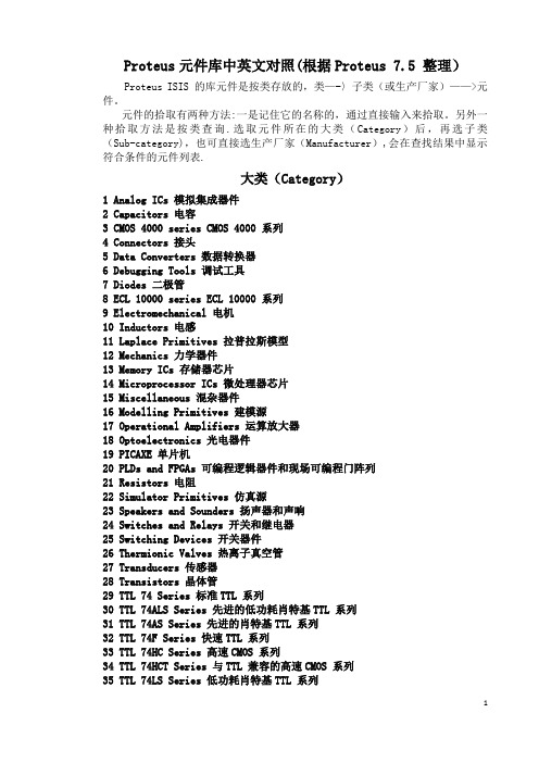
十八、Optoelectronics(光电器件)
1 14—Segment Displays 14 段显示
2 16—Segment Displays 16 段显示
3 7- Segment Displays 7 段显示
4 Alphanumeric LCDs 液晶数码显示
5 Bargraph Displays 条形显示
6 Dot Matrix Displays 点阵显示
2 Digital(Buffers&Gates) 数字(缓冲器和门电路)
3 Digital(Combinational) 数字(组合电路)
4 Digital(Miscellaneous) 数字(混杂)
5 Digital(Sequential) 数字(时序电路)
6 Mixed Mode 混合模式
7 PLD Elements 可编程逻辑器件单元
12 PIC16 Family PIC16 系列
13 PIC18 Family PIC18 系列
14 PIC24 Family PIC24 系列
15 Z80 Family Z80 系列
十五、Miscellaneous(混杂器件)
无子类
十六、Modelling Primitives(建模源)
1 Analog(SPICE) 模拟(仿真分析)
1 Audio 音频接头
2 D—Type D 型接头
3 DIL 双排插座
4 FFC/FPC Connectors 挠性扁平电缆/挠性印制电缆接头
5 Header Blocks 插头
6 IDC Headers 绝缘层信移连接件接头
7 Miscellaneous 各种接头
Schottky二极管的研制
第22卷第3期半导体学报Vol .22,No .32001年3月C~INESE J0URNAL 0F SEMIC0NDUCT0RSMar =================================================================.,2001Z~ANG Yu -ming Ph .D ,associate professor ,Was born in 1965.~is Work includes in novel semiconductor devices ,TCAD and VLSICAD .In particular ,his current research interests focus on modeling and simulation ,process technologies and devices physics for SiC -based devices .Z~ANG Yi -menmale ,professor ,Ph .D s advisor ,Was born in 1941.~e achieves great attainments in the field of device modeling and simulation in VLSI ,VLSI CAD ,guantum Well devices ,IC and high temperature microelectronics in Wide band gap semicon-ductor .Received 150ctober 2000,revised manuscript received 4December 2000Oc 2001The Chinese Institute of Electronics Fabrication of 4H -SiC merged PN -Schottky DiodesZ~ANG Yu -ming 1,Z~ANG Yi -men 1,P .Alexandrov 2and J .~.Zhao2(1Instztute Of M z 61O e Z e 6t 1O nz 6s ,X z c z c n U nz U e 1szt y ,X z c n710071, C zn c D(2D e pc1t m ent Of EZ e 6t 1z 6cZ c n c COmp ute 1E n g znee 1zn g ,T e S t c te U nz U e 1szt y OfN e I J e 1se y ,NJ 08854-8058,USA DA bstract ,The design ,fabrication and characteristics of 4~-SiC merged PN -Schottky (MPS D diodes With Ni Schot-tky contact and unction termination extension (JTE D edge termination are reported .A multiple -energy implanta-tion Al in the surface of the ndrift region beloW the face -to -face Schottky metal formed pn unctions ,Whichscreen the Schottky contact from high electrical ,post implantation annealing has been done at 1500 for 30min in the ultra -high purity Ar ambient .The devices can block more than 600V reverse voltage and the loWest leakagecurrent at 600V is 1>10 3A /cm 2,While the forWard current density at 3V is more than 200A /cm 2for 1000l m devices ,1000A /cm 2at 3.5V for 300l m devices .K ey W ords ,poWer devices G SiC G semiconductor diode G MPS EEA CC ,2560~G 2550G 2520MP A CC ,7340LC L C n Lm ber ,TN 311-.7Doc Lm ent code ,AA rtic I e I D ,0253-4177(2001D 03-0265-061I ntrod L ctionSilicon carbide (SiC D is a possible candidate toreplace the silicon -based devices in the market of high poWer devices .The potentials of SiC poWer devices Were clearly demonstrated several years ago[1].The state -of -the -art high voltage poWer de-vices have been revieWed in Reference [2].The highest reverse blocking voltage for a 4~-SiC recti-fier reported is about 5000V so far .SiC M0SFETs have been demonstrated loWer in the on -resistance than that of the silicon device .At room tempera-ture ,the 5000V IG B T and GT0have a loWer for-Ward drop than the poWer M0SFET When the cur-rent densities exceed 100A /cm 2.~oWever ,at ahigher temperature ,both the GT0and the IG B Tare superior .Experimentally ,both n -and p -chan-nel IG B T s have been demonstrated in either 6~-or 4~-SiC up to 800V ,but the forWard drop is still far from the optimal one .The symmetric and asymmetric 4~-SiC gate -controlled thyristors re-ported have the breakdoWn voltage up to 1000V and current -handling capabilities up to 6A .B oth tWo -and three -terminal devices are needed to construct the basic poWer circuit units ,such as a half -bridge circuit .The most common tWo -terminal devices are Schottky and PIN recti-fiers .The main advantage of a PIN diode is its loWer leakage current under the reverse biases ,While its disadvantage is that its forWard turn -on voltage is inherently higher than that of a Schottkydiode,as is especially true for a Wide-bandgap semiconductor SiC.Another problem of the PIN diode is the carrier storage during the on-state, Which results in a sWitching delay When it is driven from the forWard conduction to the reverse block-ing.0n the other hand,a Schottky diode has the advantages of a loW turn-on voltage and fast tran-sient recovery.oWever,due to the Schottky bar-rier height,the Schottky diode can never achieve the loW leakage current of the PIN diode.The Well-knoWn Schottky barrier loWering With the im-age force,Which results in an exponential increase of reverse current With the sguare root of the field strength(J R~exp ~(E)),is more crucial in SiC due to its extreme high critical electrical field strength(3MV/cm).The increased leakage through the Schottky barrier contact is fairly pro-nounced at high temperatures,during Which the SiC devices are expected to be used.To combine the best features of these tWo rec-tifiers,merged PN-Schottky(MPS)diode With the hybrid rectifier structure has been proposed by WilamoWski[3]for Si and demonstrated by eld et al.for SiC[4].It combines the forWard characteris-tics of the Schottky diode With the reverse property of the PN diode,and the tradeoff in it betWeen the device reverse leakage current and the forWard voltage drop can be overcome because the device reverse characteristics are determined by PN junc-tions of the device instead of the Schottky barrier height.ence,it is possible to reduce the MPS for-Word voltage drop by using a toWer-barrier contact metal,Without increasing the reverse leakage cur-rents.The principle of MPS has been experimentally demonstrated in SiC[4,5].oWever,the fabricated devices have not been optimized With respect to the tradeoff betWeen forWard conduction and reverse blocking.Geometrical shapes and junction guali-ties can be adjusted to fully optimize the device. Advanced termination technigues apply to those devices With the maximum blocking capabilities ob-tained.So,further study in this problem is de-sired.Some papers on SiC material characteris-tics[5 9]have been reported in China,While feW on SiC devices[1 14]have been done.In this paper, the design,fabrication and characterization of4-SiC MPS diodes are reported.2Design and f abricationFigure1shoWs the conceptual illustration of the SiC MPS diode to be investigated in this paper. In this device,the n-4-SiC epitaxial layer is groWn on the n+4-SiC substrate.0n the surface of the main device area,p+implanted regions al-ternate With the unimplanted one With spacing of several microns.A Schottky contact is designed to cover both the implanted regions and theunim-FIG.1Schematic Cross-Sectional VieW ofSiC MPS Diodeplanted ones.The substrate ohmic contact being under a positive applied bias,the depletion region Will spread from the Schottky interface made by the Schottky contact and the unimplanted region. At the same time,they Will also spread from p-n interfaces made by the n-epitaxial layer and the p+implanted regions.At a certain high bias,the depletion regions from the p-n junctions touch each other,as shields the Schottky interfaces from the higher electric fields.Thus,the leakage currents through the Schottky interface are effectively sup-pressed.When a forWard bias is applied,the Schottky interfaces turn on and start to conduct currents at a relatively loW bias,Which is deter-mined by the Schottky barrier height.0nly the ig-662半导体学报22卷norable loW current floWs through the p-n junc-tions because they Will not turn on until a much larger bias is applied.Therefore,the carrier injec-tion from the p+regions to the n-epitaxial layer is kept minimum,assuring the fast reVerse transient recoVery.Besides the design of the MPS in the main de-Vice area,it is necessary to design the junction ter-mination properly at the periphery of the deVice to make the reVerse blocking Voltage close to the breakdoWn Voltage of the planar structure and to suppress the leakage currents along the periphery. In this paper,a neW junction-termination-exten-sion(JTE)structure is employed.As shoWn in Fig.1,the structure is made by using the same p+ implantation in the MPS and the subseguent step-Wise etchings.OWing to the gradual thinning of the p+implantation extension,the reVerse bias gradually terminates near the periphery,suppress-ing the appearance of the Very high electric field. In addition,the outmost deeper etching proVes the complete termination of the implanted surface.For these deVices,a neW structure With improVed JTE parameters,namely three-step JTE structure,has been used.Different types of deVices Were implemented in the mask set.The contact diameter of all types of diodes is either1000pm or300pm.The implanta-tion Width c is 1.5pm,and the spacing s Varies from2pm to3pm.For JTE,the Widths l1,l2and l3are75,75and50pm,respectiVely.Detailed fabrication steps:n-/n+4-SiC epi-taxial Wafers used in the fabrication are purchased from Cree Research,Inc.The thickness and doping concentration of the epitaxial layer are6pm and 2.3>1016cm-3,respectiVely.The thickness and resistiVity of the substrate are35.56pm and 0.018 0.0190cm,respectiVely.The Wafers are of the production grade With loW micropipe density of21cm-2.The Wafers Were diVided into smaller pieces,and cleaned in the folloWing seguence:ace-tone With ultrasonic;oxygen plasma cleaning in the ICP chamber;F49%for10min With ultra-sonic;2SO4+2O2(4:1)at90C for20min.A multiple-energy implantation Al has been done at room temperature With thick photoresist mask.The implantation conditions are summarized in Table1.The implantation profile,as simulated by ProfileCode TM(Implant Sciences Corp.),is shoWn in Fig.2.The aVerage concentration of the box profile is about2>1018cm-3,With a depth of 0.65pm about.The p-n junction depth,Which cor-responds to the point Where the implanted concen-tration eguals the background doping of1016cm3,is about0.8pm.The actual profile,after the post-implantation annealing is expected to be as deep as 1.0pm.Table1Aluminum Implantation ConditionsIon Energy/keV Dose/cm-2 1Aluminum600 5.2>10132Aluminum380 3.2>10133Aluminum235 2.5>10134Aluminum135 1.6>10135Aluminum709.0>10126Aluminum30 5.0>1012Post implantation annealing to actiVate the im-planted Al dopant Was done in an ultra-high purity Ar ambient in a conVentional furnace at1500C for 30min,during Which,the samples Were aspectant With the dummy SiC Wafers to protect the sample surface.After the annealing,the samples Were cleaned by the folloWing procedures in turn:ace-tone With ultrasonic;oxygen plasma cleaning in the ICP chamber;F49%for10min With ultra-sonic;2SO4+2O2(4:1)at90C for20min; standard RCA cleaning procedure.After the implantation and annealing,the edge termination Was done on the samples.First-ly,the mesa termination is formed by ICP etching With a350nm Al etching mask.The etched depth Was3.0pm,and the first,second and third JTE etched depth Was0.29,0.03,and0.03pm,re-spectiVely.Surface passiVation Was formed by the thermal oxidation of an oxidized layer of50nm in thickness and then coVered by1.0pm LPCVD SiO2 layer.350nm Ni layer Was deposited by sputtering7623期Z ANG Yu-ming et al.:Fabrication of4-SiC Merged PN-Schottky Diodeson the backside and annealed at 1050C for 5min in the forming gas (~2=Ar =5%=95%)to form an ohmic contact .Then the top -side Schottky contact Was formed .Ni (100pm )and Al (300nm )Were de-posited by sputtering and patterned by lift -off in acetone .During that ,Ni served as a Schottky con-tact While Al as an overlay metal.FIG .2Simulation Results of Al Implantation inDevice Fabrication3DeVice CharacterizationFor the first time ,the fabricated MPS diodesWere visually inspected through an optical micro-scope .Bad devices With defects ,such as defects in the original epitaxial Wafer and the imperfections of photolithography Were rejected ,While the rest Would be further tested electrically .With devices immersed in FluorinertTMelectronic liguid ,the re-verse leakage current and the blocking voltage Were tested by using a computer controlled test setup ,Which consisted of a Keithley 248high volt-age source and Keithley 6517A digital electrometer .The forWard characteristics Were tested With an ~P 4145B semiconductor parameter analyzer and Tektronix 371A curve tracer When the devices are exposed to open air .All tests Were performed at room temperature .Figure 3shoWs three typical 1-V curves for 4~-SiC MPS diodes With diameter 1000pm and Ni Schottky contact ring Width being 2pm .It is shoWn that the leakage current density at -600VFIG .31-V Characteristics of MPS Diode With1000pm Diameter and Ni Contactis less than 10-3A /cm 2.The forWard current densi-ty at 3V is more than 200A /cm 2.From the reversecharacteristics ,We can see that the Type -Ire-verse leakage current is similar to the current of PN diode ;type -1is more like the Schottky diode ,especially When the reverse bias is beloW 200V ;type -Iis a typical MPS curves as We expected .The reason the leakage currents are different is that the thick photoresists masks for p ring im-plantation are not uniform and the implantation Widths c are various .In any case ,the reverse characteristics are determined by the screening ef-fect of the p -n junctions .The Schottky barrier height is not an important factor for the reverse leakage current if the reverse bias is very large .The breakdoWn voltage of the MPS is about 600V .More than 70%of the parallel plane junction volt-age have been achieved ,as proves the junction -ter-mination -extension(JTE )structure effective .Many of the big diodes (having a diameter of 1000pm )Will break doWn When the reverse bias is beloW 50V and the yield is less than 10%,because there are many micropipes in the Wafer as Well as some defects induced in the process of etching ,etc .~oWever ,as for the small devices (having a di-ameter of 300pm ),the yield is more than 80%,though the leakage current and the breakdoWn voltage are almost the same ,as is shoWn in Fig .4(a ).862半导体学报22卷FIG .4(a D ReVerse Characteristics of MPS Diode With3OO pm Diameter and NiContactFIg .4(b D ForWard Characteristics of MPS Diode With 3OO pm Diameter and Ni ContactFrom the forWard 1-V characteristics ,the turn -on Voltage of the 4~-SiC MPS diodes With Ni contact can be seen about 1.25V .The leVel -off of the forWard current at a high forWard bias is caused by the series resistance of diodes .The for-Ward current density of MPS diode is a little higher if the reVerse leakage current density is higher .Figure 4(b D shoWs the forWard 1-V characteristics of some 4~-SiC MPS deVices With diameter of 3OO pm and different Schottky contact ring Width (ranging betWeen 2pm and 3pm D.ObViously ,higher forWard current density can be obtained With a smaller Width of the junction implantationWindoW .The dead space beloW the junction is min-imized at the place Where the current does not floW .For 3pm deVices ,the forWard current densi-ty is higher than 1OOO A /cm 2at 3.5V (on -state re-sistance R on =3.5m0-cm 2D While it is higher than6OO A /cm 2for 2pm deVices .Why small deVices haVe high forWard current density is not clear at this moment .4Summary and conclusion4~-SiC MPS diodes With Ni Schottky contactand junction termination extension (JTE D edge ter-mination haVe been successfully designed ,fabricat-ed and characterized .The deVices can block more than 6OO V reVerse Voltage ,Which is about 7O%of the parallel plane junction breakdoWn Voltage ,andthe loWest leakage current at -6OO V is 1>1O -3A /cm 2,While the forWard current density at 3V is more than 2OO A /cm 2for 1OOO pm deVices ,1OOO A /cm 2at 3.5V for 3OO pm deVices .It shoWs that thereVerse characteristics of the reVerse leakage cur-rent are determined by the screening effect of the p -n junctions .It demonstrates that loWer barrier Schottky metal can be used for MPS diode fabrica-tion ,With Which ,loWer turn -on Voltage can be ob-tained ,While our keeping the loW reVerse leakagecurrent .Further efforts are needed to optimize the fabrication in order to get a loWer reVerse leakage and higher forWard conduction .Ref erences[1]Z~ANG Yuming and Z~ANG Yimen ,SiC PoWer DeVices .Electronic Science and Technology Letter ,1996,z9(11D :24 29(in Chinese D [张玉明,张义门,SiC 功率器件,电子科技导报,1996,z9(11D :24 29].[2]T .P .ChoW ,Materials Science Forum ,2OOO,338 34z :1155 116O.[3]B .M .WilamoWski ,Solid -State Electronics ,1983,z 6:491 495.[4]R .~eld ,N .K aminski and E .Niemannn ,Materials Science Forum ,1998,z 64 z 68:1O57 166O.[5]F .DalG uist ,C .-M .Zetterlink ,M .Ostling and K .Rottner ,Materials Science forum ,1998,z 64 z 68:1O61 1O64.9623期Z~ANG Yu -ming et a .:Fabrication of 4~-SiC Merged PN -Schottky Diodes[6]YU Ming-bin,MA Jian-ping,LUO Jia-jun and C~EN Zhi-ming,Nanocrystalline SiC Films GroWn Si by~FCVDMethod and its Photoluminescence,Chinese Journal of Semi-conductors,2000,2l:673 676(in Chinese)[余明斌,马剑平,罗家骏,陈治明,在硅衬底上用~FCVD法生长的纳米薄膜及其室温光致发光,半导体学报,2000,2l(7):673 676].[7]WANG Yinshu,LI Jinmin,Z~ANG Fangfang and LINLanying,GroWth of3C-SiC on Si(100),Chinese Journal ofSemiconductors,1999,20:630 633(in Chinese)[王引书,李晋闽,张方方,林兰英,Si(100)面3C-SiC上的生长,半导体学报,1999,20(7):630 633].[8]LI Ningsheng,BAO Ximao,LIAO Liangsheng et al.,Preparation of Si-Based Nanocrystalline SiC and its Mi-crostructure Analyses,Chinese Journal of Semiconductors,1997,l8:731 733(in Chinese)[李宁生,鲍希茂,廖良生,等,硅基纳米SiC的制备及其微结构分析,半导体学报,1997,l8(10):731 733].[9]WANG~uiyao,Wang Yinyue,SONG Ging et al.,Effect ofArgon Ion Bombardment on Formation of6~-SiC Preparedby Annealing of RF Sputtering O-SiC=~Film,ChineseJournal of Semiconductors,1998,l9(8):569 573(in Chi-nese)[王辉耀,王印月,宋青,等,氩离子轰击对射频溅射法制备的O-SiC=~膜退化形成6~-SiC的影响,半导体学报,1998,l9(8):569 573].[10]Z~ANG Yuming,Luo Jinsheng and Z~ANG Yimen,Au/NiCr Ohmic Contacts on n-type6~-Silicon Carbide,ChineseJournal of Semiconductors,1997,l8(9):718 720(in Chi-nese)[张玉明,张义门,罗晋生,n型6~-SiC体材料欧姆接触的制备,半导体学报,1997,l8(9):718 720].[11]Z~ANG Yuming,Z~ANG Yimen and LUO Jinsheng,PtSchottky Barrier Diodes on n-type6~-Silicon Carbide,Chi-nese Journal of Semiconductors,1999,20(11):1040 1043(in Chinese)[张玉明,张义门,罗晋生,SiC肖特基势垒二极管的研制,半导体学报,1999,20(11):1040 1043].[12]Z~ANG Yuming,Z~ANG Yimen and LUO Jinsheng,Studyof6~-SiC MOSFET,Research8Progress of Solid StateElectronics,2000,20(1):1 6(in Chinese)[张玉明,张义门,罗晋生,6~-SiC MOS场效应晶体管的研制,固体电子学研究与进展,2000,20(1):1 6].[13]Yuming Zhang and Yimen Zhang,~igh-Field and~igh-Tem-perature Transport in n-type3C-SiC,The2nd InternationalConference on Modeling and Simulation of Microsystem,Semiconductor,Sensors and Actuators,San Juan,Puerto Ri-co,USA,April19,1999.[14]WANG Shu-rui,LIU Zhong-li,XU Ping et al.,6~-SiC~igh Voltage Schottky Barrier Diodes,Chinese Journal ofSemiconductors,to be published(in Chinese)[王姝睿,刘忠立,徐萍,等,6~-SiC高压肖特基势垒二极管,半导体学报,待发表].4H-SiC混合PN/Schottky二极管的研制张玉明1张义门1P.Alexandro V2J.~.Zhao2(1西安电子科技大学微电子所,西安710071,中国)(2Department of Electrical and Computer Engineering,The State Uni V ersityof NeW Jersey,NJ08854-8058,USA)摘要:报道了4~-SiC混合PN/Schottky二极管的设计,制备和特性.该器件用镍作为肖特基接触金属,使用了结终端扩展(JTE)技术.在肖特基接触下的n型漂移区采用多能量注入的方法形成P区而组成面对面的PN结,这些PN结将肖特基接触屏蔽在高场之外,离子注入的退化是在1500C下进行了30min.器件可耐压600V,在600V时的最小反向漏电流为1>103A/cm2.1000p m的大器件在正向电压为3V时电流密度为200A/cm2,而300p m的小尺寸器件在正向电压为3.5V电流密度可达1000A/cm2.关键词:功率器件;碳化硅;半导体二极管;MPSEEA CC:2560~;2550;2520M P A CC:7340L中图分类号:TN311-.7文献标识码:A文章编号:0253-4177(2001)03-0265-06张玉明男,1965年出生,博士,副教授,从事新型半导体器件,TCAD和VLSI CAD的教学和科研工作.目前主要研究碳化硅器件的器件物理,工艺,模型和模拟.张义门男,1941年出生,教授,博士导师,主要从事VLSI中器件的模型和模拟,VLSI CAD,量子阱器件和宽禁带高温微电子学.2000-10-15收到,2000-12-04定稿c2001中国电子学会072半导体学报22卷4H-SiC混合PN/Schottky二极管的研制作者:张玉明, 张义门, P.Alexandrov, J.H.Zhao, ZHANG Yu-ming, ZHANG Yi-men,P.Alexandrov, J.H.Zhao作者单位:张玉明,张义门,ZHANG Yu-ming,ZHANG Yi-men(西安电子科技大学微电子所,),P.Alexandrov,J.H.Zhao,P.Alexandrov,J.H.Zhao(Department of Electrical andComputer Engineering,The State University of New Jersey,)刊名:半导体学报英文刊名:CHINESE JOURNAL OF SEMICONDUCTORS年,卷(期):2001,22(3)被引用次数:10次1.张玉明;张义门SiC功率器件 1996(11)2.T P Chow查看详情[外文期刊] 20003.B.M.Wilamowski查看详情 19834.R Held;N Kaminski;E Niemannn查看详情 19985.F Dalquist;C-M Zetterlink;M Ostling查看详情 19986.余明斌;马剑平;罗家骏;陈治明在硅衬底上用HFCVD法生长的纳米薄膜及其室温光致发光[期刊论文]-半导体学报 2000(07)7.王引书;李晋闽;张方方;林兰英,Si(100)面3C-SiC上的生长[期刊论文]-半导体学报 1999(07)8.李宁生;鲍希茂;廖良生硅基纳米SiC的制备及其微结构分析[期刊论文]-半导体学报 1997(10)9.王辉耀;王印月;宋青氩离子轰击对射频溅射法制备的α-SiC:H膜退火形成6H-SiC的影响[期刊论文]-半导体学报 1998(08)10.张玉明;张义门;罗晋生n型6H-SiC体材料欧姆接触的制备[期刊论文]-半导体学报 1997(09)11.张玉明;张义门;罗晋生SiC肖特基势垒二极管的研制[期刊论文]-半导体学报 1999(11)12.张玉明;张义门;罗晋生6H-SiC MOS场效应晶体管的研制[期刊论文]-固体电子学研究与进展 2000(01)13.Yuming Zhang;Yimen Zhang High-Field and High-Temperature Transport in n-type 3C-SiC,The 2nd International Conference on Modeling and Simulation of Microsystem,Semiconductor 199914.王姝睿;刘忠立;徐萍6H-SiC高压肖特基势垒二极管[期刊论文]-半导体学报 2001(08)1.苗永斌.张玉明.张义门4H-SiC MPS二极管反向恢复特性的仿真研究[会议论文]-20032.牛新军.张玉明.张义门.吕红亮碳化硅混合PiN/Schottky二极管的二维模拟[期刊论文]-半导体学报2002,23(5)3.张玉明.牛新军.张义门SiC和Si混合PiN/Schottky二极管的模拟和设计[期刊论文]-电力电子技术2002,36(1)4.张玉明.牛新军.张义门SiC混合PiN/Schottky二极管(MPS)的研究[会议论文]-20015.牛新军4H-SiC混合PiN/Schottky(MPS)二极管的研究[学位论文]20026.牛新军.张玉明.张义门.吕红亮.常远程碳化硅MPS的功率损耗特性分析[期刊论文]-固体电子学研究与进展2003,23(2)7.韩颖晖.汪再兴.闫锐.杨建红.HAN Ying-hui.WANG Zai-xing.YAN Rui.YANG Jian-hong短漂移区肖特基-p-i-n混合整流二极管(MPS)的电学特性研究[期刊论文]-兰州大学学报(自然科学版)2006,42(3)8.苗永斌.张玉明.张义门碳化硅MPS:新一代功率开关二极管[期刊论文]-微电子学2004,34(2)。
超级结MOSFET中集成肖特基二极管的方法[发明专利]
![超级结MOSFET中集成肖特基二极管的方法[发明专利]](https://img.taocdn.com/s3/m/e703258658fafab068dc0200.png)
专利名称:超级结MOSFET中集成肖特基二极管的方法专利类型:发明专利
发明人:邱慈云,张帅,刘坤
申请号:CN201010605854.4
申请日:20101227
公开号:CN102569207A
公开日:
20120711
专利内容由知识产权出版社提供
摘要:本发明公开了一种在超级结MOSFET中集成肖特基二极管的方法,为在所述超级结MOSFET中并联集成有由肖特基接触与衬底形成的肖特基二极管,其中所述肖特基二极管的阳极设置在超级结MOSFET芯片的元胞区域源端的相邻两个体区之间,所述肖特基二极管的阳极与所述超级结MOSFET的源端相连,所述肖特基二极管的阴极共用位于衬底背面的漏电极。
超级结MOSFET并联肖特基二极管的结构,利用肖特基二极管的快速开关特性提高超级结MOSFET器件的反向恢复速度。
申请人:上海华虹NEC电子有限公司
地址:201203 上海市浦东新区川桥路1188号
国籍:CN
代理机构:上海浦一知识产权代理有限公司
代理人:丁纪铁
更多信息请下载全文后查看。
- 1、下载文档前请自行甄别文档内容的完整性,平台不提供额外的编辑、内容补充、找答案等附加服务。
- 2、"仅部分预览"的文档,不可在线预览部分如存在完整性等问题,可反馈申请退款(可完整预览的文档不适用该条件!)。
- 3、如文档侵犯您的权益,请联系客服反馈,我们会尽快为您处理(人工客服工作时间:9:00-18:30)。
*Project supported by National High T echnology Research and Development Program of China(No.2003AA1Z1280) Li Qiang male,PhD candidate.His research field emphases on analog integrate circuit design.Email:liqi ang@ Received 24M ay 2004,revised manuscript received 2August 20042005Chi n ese Ins titute of Electron i csDesign and Fabrication of Schottky Diode withStandard CMOS Process *Li Qiang,Wang Junyu,Han Yifeng,and M in Hao(S tate K e y L abor atory o f AS IC&Syste m ,Fudan Univ ersity ,S hanghai 200433,China)Abstract:Desig n and fabrication of Schottky bar rier diodes (SBD)w ith a commer cial standard 0 35 m CM OS process are described.I n order to reduce the series resistor of Schottky contact,interdigitating the fingers of scho ttky diode layout i s adopted.T he I V ,C V ,and S parameter are measured.T he parameters of realized SBD such as t he saturation cur rent,breakdow n voltage,and the Schottky barr ier heig ht are given.T he SPI CE simulation model of the realized SBDs is g iven.Key words:CM O S;Schottky dio de;integration EEAC C:2560H;2570DC LC number:T N311+7 Document code:A Article ID:0253 4177(2005)02 0238 051 IntroductionSchottky diodes have advantages such as fast sw itching speed and low forward voltage drop.Due to these ex cellent hig h frequency performance,they have been w idely used in pow er detection and microwave network circuit[1].Schottky diodes are often fabricated by depositing metals on n ty pe or p type semicon ductor materials such as GaAs and SiC [2~4].Theproperties of forw ard biased Schottky diodes are de termined by m ajority carrier,while minority carrier prim arily determine those properties of p n diodes.In order to improve high frequency performance and de crease supply voltage of IC,integ rating the Schottky diode into modern IC is very important.But the pro cess that can integrate Schottky diode is often not commercially available and not to integrate with CM OS circuits monolithically.Design about it has ev er been introduced and the fabrication of Schottky in standard CMOS process w ith the additional CMOS process has been repoted w hile not show n the measured results [5,6].In this paper w e describe the w ay todesign and layout a Schottky diode in a low cost com mercial standard CM OS process w ithout any processmodification.The measured results and SPICE simu lation model are offered.2 Design and layout of Schottky diodeThis design w as performed throug h M PW(multi project wafer)in charted 0 35 m CM OS process.A Schottky diode is form ed w hen a metal layer is de posited directly onto a low doped n type or p type sem iconductor region.When these tw o materials are brought into contact with each other,the difference in potential g ives rise to a barrier heig ht that the elec trons have to overcom e for current to flow.The metal on the low doped semiconductor is the anode and the sem iconductor material,w hich contacted through an ohm ic contact,is the cathode.In our design only n type Schottky diodes w ere used.A cross section of the Al Si Schottky diode is show n in Fig.1.第26卷 第2期2005年2月半 导 体 学 报CHI NESE JOU RNAL OF SEM ICON DUCT ORSVol.26 No.2 Feb.,2005Fig.1 Cross section of Al Si SchottkyIn our design,there w as no p+active reg ion un der the contact in n well,the contact material is alu m inum w ith area A(equal to d d).Therefore,the metal layer will connect directly to the low doped n w ell.As a result there forms a Al Si Schottky diode contact.For the foundry process determines most of the parameters such as w ork function of metal and density of n well,w e can only control the area A of Schottky diode to modify the I V curve or other pa rameters of the diode.Fig ure2show s the layout of designed Schottky diode.In order to reduce the series resistance of the Schottky diode,firstly,the distance betw een the Schottky and ohmic contacts w as set to the minimum allow able according to the design rules.Secondly,in terdigitating the fingers of Schottky diode layout w as adopted.The interdigitated layout offers the advan tage of parallel connecting of each series resistance un der Schottky contact.3 Measurement results of the fabricated diodeThree types of interdigitating fingers Schottky diodes w ith different area have been fabricated in the charted standard0 35 m CM OS process throug h M PW.The measured results are discussed.3.1 I V performanceConsidering the series resistor,the I V function of Schottky diode can be express as[7]I=I s exp(V-IR snV t)1-exp(V-I R sV t)(1)F ig.2 (a)Cross section layout of t he r ealized Schottkydiode;(b)P lane section layout of the r ealized Schottkydiodew here V is the bias voltage,I s is the saturation current,R s is the series resistor,V t is the therm al voltagew hich equals to kT/q,and n is the SBD ideality factor which can be calculated as:n=I/(V td Id V)(2)If the bias voltage is larger than3kT/q,Equation(1)can be sim plified asI=I s ex p(V-I R sn V t)(3)And the Schottky barrier heig ht B can be calculatedasB=V t ln(A A*T2I s)(4)w here A*is the effective Richardson constant.The measured I V curve is show n in Fig.3.By fitting Eq.(3)and the m easured results,wecan get the parameters of the realized SBDs,w hich areshow n in T able1.T able1 P ar ameters of the realized SBDArea/ m2Finger number I s/A R s/SBD116102 10-810SBD2 1.625 10-990SBD30.6401 10-9200From T able1,w e can observe that w ith thenumber of interdig itating fingers increasing,the seriesresistance can be reduced evidently.239第2期Li Q iang et al.: Desig n and Fabricatio n of Schottky Diode w ith Standard CM OS ProcessF ig.3 (a)M easured I V cur ves at forward bias;(b)M easur ed I V curves at rever se bias Area of SBD1,SBD2,and SBD3ar e r espectively 16,1 6,and 0 64 m 2.T he measured statistic result of barrier height Bfor the realized SBD is show n in Fig.4.There are to tal 90samples that have been measured (30samples for each of SBD1,SBD2,SBD3).And the barrier height of the realized SBD is about 044eV.F ig.4 Statistic result of B for the measur ed SBD (total 90samples)The breakdow n voltage is about 4 5V.In future w ork,the breakdow n voltage can be ex tended by some methods that have been used in normal SBD de sig n,such as the fabrication of SBD w ith self alig ned guard ring[8].3.2 C V performanceThe small signal junction capacitor C j of Schot tky diode is g iven below,C j =Aq s N d2( B - n -V)(5)w here N d is the doping concentration of the n w ell, n is the potential difference betw een the fermi level and the conduction band edge w hich equals to (E C -E f)/q.Figure 5shows the measured reverse bias C V curve for SBDs.Fig.5 M easured C V curve f =2 4GHz3.3 S parameter measurement and SBD high frequency modelingIn order to measure the high frequency S param eter of the designed devices,each SBD w as laid w ith three probe pads.The size of middle signal pad is 85 m 85 m and top/bottom g round size is 85 m 135 m.U sing the GSG probe and netw ork analysis instrument,w e can get the S parameter of the de sig ned SBD.But the directly measured results of Sparameter include the parasitic capacitance of pads,metal line and overlays.For the designed device is very small,these parasitic parameters could not be ne240半 导 体 学 报第26卷g lected and must be subtracted from the directly mea sured S parameter by GSG probe.In our w orks,w e fabricated two dummy GSG pads w ith no tested de vice.The dummy pads size is the same as that includ ing SBD.One dummy GSG pads signal is connected w ith GND called short pad.The other dummy GSG pads sig nal is open w hich is called open pad.The S parameter of dummy pads should be measured.Then w e can get the parasitic capacitance and resistance of the pad and metal line.And subtracting these parasitic parameter w e can get the S parameter of SBDs with no parasitic capacitance and resistance.T his method is called de embedding technology [9].U sing the measured S parameter,the SPICE model can be abstracted for high frequency simula tion.Figure 6show s the simulation model of the real ized SBD.L 1and L 2ex hibit the input and output se rial inductance.C i and C o exhibit the anode input and cathode node output capacitance respectively.C 1ex hibits the parasitic capacitance betw een the interdigi tating fingers of Schottky diode s two ports.R 1and R 2model for the resistance under the n w ell w hich connects the place under NWLL to ground.T he pn diode reflects the parasite n w ell p sub diode.In our design,the parameter of the pn diode can be gotten from the charted 0 35 m analog CMOS process SPICEmodel.F ig.6 Simulatio n model of the r ealized SBDFig ure 7show s the measured and simulation S parameter of SBD1(after de em bedding ).Table 2shows the parameter of SBD1by the simulation mod el.The frequency is swept from 50MHz to 40GH z.And the model can match the measured results up to 30GHz.Figure 8show s the photo of realized SBD under probemeasurement.Fig.7 M easurement and simulation S parameter of SBD1from 50M Hz to 40GHz after deembeddingFig.8 Photo of the realized SBD under GSG pr obe mea sur ementT able 2 Component value of SBD1L 10.005nH L 20.005nH C i 0.01pf C o 0.05pf R 1200 R 2200 C 10.14pf I s 2 10-8A R s 10 C j00.022pf B v4.5VNbv234 ConclusionFabrication of Schottky barrier diode in standard CMOS process throug h M PW are performed.T he barrier heig ht of the Al nSi contacts is about 0 44eV.The measured I V ,C V ,and S parameter of the re241第2期Li Q iang et al.: Desig n and Fabricatio n of Schottky Diode w ith Standard CM OS Processalized SBDs are show n in this paper.The advantages of this SBD design are low cost and can be integ rated into commercial standard CM OS process.In the fu ture w ork,more emphasis w ill be focused on extension of the reverse breakdow n voltage and frequency range of the SBDs designed on standard CM OS process.References[1] Sharma B L.M etal semiconductor Schottky barrier junctionsand th eir applications.New York:Plenum,1984[2] Hudait M K,Vankatesw arlu P,Krupanidhi S B.Electricaltransport characteristics of Au/n GaAs Schottky diodes on n Geat low temperatures.Solid S tate Electron,2001,45(1):133 [3] Zhang Yuming,Zhang Yimen,Alexandrov P,et al.Fabrication of4H SiC m erged PN S chottky diodes.Chinese Journal of S emiconductors,2001,22(3):265[4] Zhang Haiyan,Ye Zhizhen,Huang Jingyun,et al.Fabrication ofS chottky barrier diodes of high frequency based on thin siliconepilayer.Chi n ese Journal of Semiconductors,2003,24(6):622(i n Chinese)[张海燕,叶志镇,黄靖云,等.在薄硅外延片上制备高频肖特基势垒二极管.半导体学报,2003,24(6):622] [5] M ilanovic V,Gai tan M,M arshall J C,et al.CM OS foundry i mplem entation of Schottky diodes for RF detection.IE EE TransElectron Devices,1996,43(2):2210[6] Rivera B,Baker R J,M elngaili s J.Design and layout of S chottkydiodes in a standard CM OS process.International SemiconductorDevice Research Symposium,2001:79[7] Rhoderick E H.M etal semiconductor contacts.Second edition.Oxford:Ox ford University Press,1988[8] C ha S I,Cho Y H.Novel Schottky di ode w i th selfalignedguard ring.Electron Lett,1992:1221[9] Aktas A,Ismail M.Pad de embedding in RF CM OS.IEEEC i rcuit and Devices M agazine,2001,17(3):8标准CMO S工艺集成肖特基二极管设计与实现*李 强 王俊宇 韩益锋 闵 昊(复旦大学专用集成电路与系统国家重点实验室,上海 200433)摘要:提出了一种在标准CM OS工艺上集成肖特基二极管的方法,并通过M P W在charted0 35 m工艺中实现.为了减小串连电阻,肖特基的版图采用了交织方法.对所设计的肖特基二极管进行了实测得到I V,C V和S参数,并计算得出所测试肖特基二极管的饱和电流、势垒电压及反向击穿电压.最后给出了可用于SPI CE仿真的模型.关键词:CM OS;肖特基二极管;集成EEAC C:2560H;2570D中图分类号:T N311+ 7 文献标识码:A 文章编号:0253 4177(2005)02 0238 05*国家高技术研究发展计划资助项目(批准号:2003AA1Z1280)李 强 男,博士研究生,研究方向为模拟集成电路设计.Email:li qiang@2004 05 24收到,2004 08 02定稿 2005中国电子学会242半 导 体 学 报第26卷。
