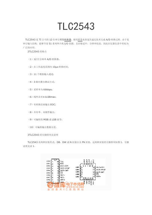
TLC2543的特性
新型数转换器TLC2543的串行接口及其应用

( 德州仪器 公司) 为接 口的主要部 分 。 微 处理器 可以用软件配置为 S I P 的主机或从机 。当 作为主机 , 数据通过 SI ( O I从机输出主机输入) R 管脚输^ 到 SI P 移位 寄存器 (P D T 。同时数据通过 s M ( 5 IA ) IO 从机 输入主机输 出) 管脚从 S] P 移位寄存器 (P D T 输 出。 S IA ) SI P 的功能如下 。 P D T S IA 必须装A要 发送数据的第
一
个 字节 。 样对 这个 字 节 的传 送 自动初 始 化 在 这 个 这
数据 传送 时间 内,数据 在 另一 个 S IA 被接收 。S I PD T P [T F A N L G定时被检查 。当数据 的最后一位 被接 收到 , S I IT F A 被 置为 1 P N LG 。这 表示接收的 数据字节可 以
统 ,并给 出三个主流 u 8 C 1 6 H 1 , M 3 0 的接 (0 5 , 8 C 1 T S 7 ) 口电路 。
2 L 2 4 简 介 .T C 5 3
● 串行数据 同时输入和输 出 ● 同步工 作 ● 提供频率可编程的 串行时钟 ● 数据传送 结束标志 图 2 示 S 1的结构 。这个例 子中用 T S 7 C l 显 P M 30 OO
图 4 T C 5 3与 6 H 1E 微处理器接 【 L2 4 8 C 2 1 = J
LB 始) 是否需要单极性 ( S开 和 二进 制) 或般 极 性 ( 进 制 二
(D) 具有 l 位 的分辨率 ,使用开关 电容逐次逼近技 AC , 2 术完成 A 转换过程 ,提供 的最大采样率为 6 K P ,供 D 6SS
TLC2543 芯片资料
IMPORTANT NOTICETexas Instruments and its subsidiaries (TI) reserve the right to make changes to their products or to discontinue any product or service without notice, and advise customers to obtain the latest version of relevant information to verify, before placing orders, that information being relied on is current and complete. All products are sold subject to the terms and conditions of sale supplied at the time of order acknowledgement, including those pertaining to warranty, patent infringement, and limitation of liability.TI warrants performance of its semiconductor products to the specifications applicable at the time of sale in accordance with TI’s standard warranty. Testing and other quality control techniques are utilized to the extent TI deems necessary to support this warranty. Specific testing of all parameters of each device is not necessarily performed, except those mandated by government requirements.CERTAIN APPLICATIONS USING SEMICONDUCTOR PRODUCTS MAY INVOLVE POTENTIAL RISKS OF DEATH, PERSONAL INJURY, OR SEVERE PROPERTY OR ENVIRONMENTAL DAMAGE (“CRITICAL APPLICATIONS”). TI SEMICONDUCTOR PRODUCTS ARE NOT DESIGNED, AUTHORIZED, OR WARRANTED TO BE SUITABLE FOR USE IN LIFE-SUPPORT DEVICES OR SYSTEMS OR OTHER CRITICAL APPLICATIONS. INCLUSION OF TI PRODUCTS IN SUCH APPLICATIONS IS UNDERSTOOD TO BE FULLY AT THE CUSTOMER’S RISK.In order to minimize risks associated with the customer’s applications, adequate design and operating safeguards must be provided by the customer to minimize inherent or procedural hazards.TI assumes no liability for applications assistance or customer product design. TI does not warrant or represent that any license, either express or implied, is granted under any patent right, copyright, mask work right, or other intellectual property right of TI covering or relating to any combination, machine, or process in which such semiconductor products or services might be or are used. TI’s publication of information regarding any third party’s products or services does not constitute TI’s approval, warranty or endorsement thereof.Copyright © 1998, Texas Instruments Incorporated。
TLC2543IDWR;TLC2543CN;TLC2543IN;TLC2543CDB;TLC2543CDW;中文规格书,Datasheet资料

– 55°C to 125°C — — — TLC2543MJ — † Available in tape and reel and ordered as the TLC2543CDBLE, TLC2543IDBR, TLC2543CDWR, TLC2543IDWR, TLC2543CFNR, or TLC2543IFNR.
On products compliant to MIL-PRF-38535, all parameters are tested unless otherwise noted. On all other products, production processing does not necessarily include testing of all parameters.
18 15
2
POST OFFICE BOX 655303
• DALLAS, TEXAS 75265
/
ห้องสมุดไป่ตู้
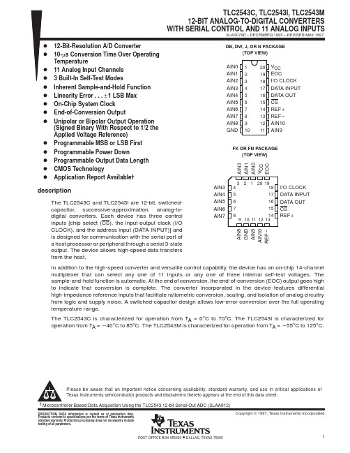
TLC2543C, TLC2543I, TLC2543M 12-BIT ANALOG-TO-DIGITAL CONVERTERS WITH SERIAL CONTROL AND 11 ANALOG INPUTS
VCC EOC I/O CLOCK DATA INPUT DATA OUT CS REF + REF – AIN10 AIN9
FN PACKAGE (TOP VIEW)
description
The TLC2543C and TLC2543I are 12-bit, switchedcapacitor, successive-approximation, analog-todigital converters. Each device, with three control inputs [chip select (CS), the input-output clock, and the address input (DATA INPUT)], is designed for communication with the serial port of a host processor or peripheral through a serial 3-state output. The device allows high-speed data transfers from the host.
基于Pt100_热电阻的简易温度测量系统毕业设计论文1 精品

基于PT100热电阻的简易温度测量仪摘要:本文首先简要介绍了铂电阻PT100的特性以及测温的方法,在此基础上阐述了基于PT100的温度测量系统设计。
在本设计中,是以铂电阻PT100作为温度传感器,采用恒流测温的方法,通过单片机进行控制,用放大器、A/D转换器进行温度信号的采集。
通过对电路的设计,减小了测量电路及PT100自身的误差,使温控精度在0℃~100℃范围内达到±0.1℃。
本文采用STC89C52RC单片机,TLC2543 A/D转换器,AD620放大器,铂电阻PT100及液晶系统,编写了相应的软件程序,使其实现温度及温度曲线的实时显示。
该系统的特点是:使用简便;测量精确、稳定、可靠;测量范围大;使用对象广。
关键词:PT100 单片机温度测量 AD620 TL431AbstractThis article briefly describes the characteristics of PT100 platinum resistance and temperature measurement method, on the basis it describes the design of temperature measurement system based on PT100. In this design, it is use a PT100 platinum resistance as temperature sensor, in order to acquisition the temperature signal, it use of constant-current temperature measurement method and use single-chip control, Amplifier, A / D converter. It can still improve the perform used two-wire temperature circuit and reduce the measurement eror. The temperature precision is reached ±0.1℃ between 0℃~100℃.The system contains SCM(STC89C52), analog to digital convert department (TLC2543), AD620 amplifier, PT100 platinum, LCD12864, write the corresponding software program to achieve real-time temperature display. The system is simple , accurate , stable and wide range. Keywords:PT100 MCU Temperature Measures AD620 TL431目录前言 (4)第一章方案设计与论证 (6)1.1 传感器的选择 (6)1.2 方案论证 (7)1.3 系统的工作原理 (8)1.4 系统框图 (9)第二章硬件设计 (9)2.1 PT100传感器特性和测温原理 (9)2.2 硬件框图以及简要原理概述 (11)2.3 恒流源模块测温模块设计方案 (11)2.4 信号放大模块 (12)2.5 A/D转换模块 (15)2.6 单片机控制电路 (18)2.7 显示模块 (19)第三章软件设计 (19)3.1系统总流程的设计 (19)3.2 主函数的设计 (20)3.3 温度转换流程图的设计 (21)3.4 显示流程图 (21)3.5 按键流程的设计 (22)第四章数据处理与性能分析 (23)4.1采集的数据及数据处理 (23)4.2 性能测试分析 (23)第五章结论与心得 (24)1 结论 (24)2 心得 (24)附录1 原理图 (25)附录2 元器件清单 (26)附录3 程序清单 (27)前言随着科技的发展和“信息时代”的到来,作为获取信息的手段——传感器技术得到了显著的进步,其应用领域越来越广泛,对其要求越来越高,需求越来越迫切。
TLC2543在波导损耗测量系统中的应用
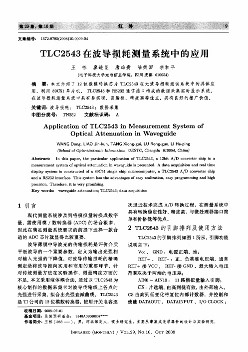
摘 要 : 文介 绍 了 l 数 模 转换 芯片 T C 5 3 光 波 导损耗 测试 系 统 中 的具 体应 本 2位 L 24 在
用 。利用 8 C 1 9 5 单片 机 、 T C 53 R 22 信接 口构 成 的数据采 集 实 时显示 系统, L 24 和 S 3 通 在 波 导损 耗测量 系统 中具有 易实现、易编程 、精 度 高等优 点,具 有 良好 的推广价 值。 关键 词:波导损耗 ; T C 53 L 24 ;数 据采集 中 图分 类号 : T 22 文献 标识码 : A N 5
(col f p o l t nc nomai , E T , h n d 104 C ia Sh o o t- e r i Ifr t n U S C C eg u 605 , hn) O eco o
Ab ta t I h ae, h at ua p l ai f L 24, 2 i A D cnetrci i sr c: nti p p r tepri l api t no C 53 a 1bt / ovr hp na s c r c o T e
me s r me t s s e fo i a t e u to n v gu d s p e e t d.A a a a q iii n a e ltm e a u e n y t m o ptc la t n a i n i wa e i e i r s n e d t c u s to nd r a i
d pa ytm i cntutdo 9 5 ig hpmi oo ue, L 24 D cne e hp i l ss o s ce f 8C 1s l ci c cmp tr aT C 53A/ o vr r i s y e s r a ne r t c
TLC2543TLC1543

TLC2543TLC1543 12位10位AD数据转换时序图:下降沿输出数据,上升沿输⼊地址CS⽚选拉低,⼀次转换开始,同时输出上次转换的数据时序使⽤⽅法:1、CS⽚选拉⾼,EOC拉⾼,CLK时钟拉低2、CS⽚选拉低,开始读出第⼀位数据3、在第⼀个时钟上升沿,输⼊⼀个地址数据4、之后在每个时钟的下降沿输出AD转换数据,在上升沿输⼊地址数据5、TLC1543是10位AD,因此有10个时钟,TLC2543是位AD,因此有12个时钟6、⼀个操作过程结束后,⽚选CS拉⾼,EOC会在最后第10个时钟的下降沿触发拉低,开始AD转换,此时,输出被禁⽌,等到转换结束后EOC置位1,代表转换结束。
等到CS⽚选再次拉低,开始第⼆次操作。
TLC1543与单⽚机的连接TLC15433的引脚图A0~A10为11个模拟输⼊通道REF-通常接地REF+接+5v则输⼊可测电压为0~5vcs位⽚选段,低电平有效,不⽤时置1,⽤时保持为0DATAOUT为AD转换数据输出端(10位)ADDRESS为地址输⼊端,可输⼊相关的命令,前四位⽤于选择不同的输⼊通道,如:0000位选择0通道,0001位选择1通道,及数据输出的格式(⾼位先出还是低位先出)。
TLC1543⼦函数uint read1543(void){uchar i=0;uint ad_value=0;TCL2543_CLK=0; //⼀次转换开始前,CS⽚选置1,EOC置1,时钟置0TCL2543_CS=1;EOC=1;delay_1ms(); //保持⼀段时间,拉低CS⽚选TCL2543_CS=0;delay_1ms(); //保持⼀段时间,等数据稳定后再读取第⼀位数据A9(最⾼位)for(i=0;i<10;i++){if(TCL2543_DOUT) ad_value|=0x0001; //读取第⼀位数据TCL2543_DIN=0; //将通道选择数据准备好,上升沿锁存进TLC1543TCL2543_CLK=1; //上升沿delay_1ms(); //保持⼀段时间TCL2543_CLK=0; //下降沿保持⼀段时间,在读取数据delay_1ms();ad_value=ad_value<<1; //移位,将最低位空出,以装⼊第2位数据(A8)}TCL2543_CS=1; //⼀次转换结束后将CS⽚选拉⾼ad_value=ad_value>>1; //由于多左移了1位,所以return ad_value;}。
12864画电压曲线
12864液晶应用1、TLC2543简介1.1 TLC2543的特点及引脚TLC2543是12 位串行A/D转换器,使用开关电容逐次逼近技术完成A/D转换过程.由于是串行输入结构,能够节省51系列单片机的I/O资源.其特点有:1)12 bit分辨率A/D转换器;2)在工作温度范围内10us转换时间;3)11个模拟输入通道;4)3路内置自测试方式;5)采样率为66kb/s;6)线性误差±1LSB(max);7)有转换结束(EOC)输出;8)具有单、双极性输出;9)可编程的MSB或LSB前导;10)可编程的输出数据长度.TLC2543的引脚排列如图1所示.图中AIN0~AINl0为模拟输入端;CS为片选端;DIN 为串行数据输入端;DOUT为A/D转换结果的三态串行输出端;EOC为转换结束端;CLK为I /O时钟;REF+为正基准电压端;REF-为负基准电压端;VCC为电源;GND为地。
2、TLC2543的使用方法2.1控制字的格式控制字为从DATA INPUT端串行输人的8位数据,它规定了TLC2543要转换的模拟量通道、转换后的输出数据长度、输出数据的格式。
其中高4位(D7~04)决定通道号,对应0通道至10通道,该4位分别为0000—1010H,当为1011—1101时,用于对TLC2543的自检测,当为11l0时,TLC2543进入休眠状态。
低4位决定输出数据长度及格式,其中D3、D2决定输出数据长度,01表示输出数据长度为8位.11表示输出数据长度为16位,其他为12位。
Dl 决定输出数据是高位先送出,还是低位先送出,为0表示高位先进出。
D0决定输出数据是单极性(二进制)还是双极性(2的补码),若为单极性,该位为0,反之为1。
2.2 TLC2543的内部寄存器从编程角度看,TLC2543内部寄存器有输入数据寄存器与输出数据寄存器。
输入数据寄存器存放从DATA INPUT端移入的控制字。
自动浇花系统设计毕业论文

DHT-11可通过I2C 总线直接输出数字量湿度值,从其相对湿度输出特性曲线中可以看出,DHT11 的输出特性呈一定的非线性,为了补偿湿度传感器的非线性以获取准确数据,可按式(3-1)修正湿度值:[]linear RH =2321RHRH SO c SO c c ++ ()13- 式中,SORH 表示传感器相对湿度测量值,系数取值分别如下:12位时:6321108.2,0405.0,4-⨯-==-=c c c ;8位时: 4321102.7,648.0,4-⨯-==-=c c c 。
(3)温度值输出DHT-11温度传感器的线性非常好,可用下列公式(3-2)将温度数字输出转换成实际温度值T :T SO d d T 21+= ()23-式中,T SO 表示传感器温度测量值。
当电源电压为5V ,温度传感器的分辨率为14位时,401-=d ,01.02=d ;当温度传感器的分辨率为12位时,401-=d ,04.02=d 。
图2-3 相对湿度输出特性曲线图2.4 土壤湿度采集模块Bardolino Moisture Sensor 土壤湿度传感器可用于检测土壤的水分,当土壤缺水时,传感器输出值将减小,反之将增大,使用AD转换器读取它的值,然后传送给单片机,单片机根据数值大小来判断是否该浇水。
AD采用了TLC2543,TLC2543是TI公司的12位串行模数转换器,使用开关电容逐次逼近技术完成A/D转换过程。
由于是串行输入结构,能够节省Bardolino系列单片机I/O资源,且价格适中,分辨率较高,因此在仪器仪表中有较为广泛的应用。
2TLC2543的特点:(1)12位分辩率A/D转换器;(2)在工作温度围10μs转换时间;(3)11个模拟输入通道;(4)3路置自测试方式;(5)采样率为66kbps;(6)线性误差±1LSBmax;(7)有转换结束输出EOC;(8)具有单、双极性输出;(9)可编程的MSB或LSB前导;(10)可编程输出数据长度。
TLC2543
TLC2543
TLC2543是TI公司的12位串行模数转换器,使用开关电容逐次逼近技术完成A/D转换过程。
由于是串行输入结构,能够节省51系列单片机I/O资源;且价格适中,分辨率较高,因此在仪器仪表中有较为广泛的应用。
2TLC2543的特点
(1)12位分辩率A/D转换器;
(2)在工作温度范围内10μs转换时间;
(3)11个模拟输入通道;
(4)3路内置自测试方式;
(5)采样率为66kbps;
(6)线性误差±1LSBmax;
(7)有转换结束输出EOC;
(8)具有单、双极性输出;
(9)可编程的MSB或LSB前导;
(10)可编程输出数据长度。
3TLC2543的引脚排列及说明
TLC2543有两种封装形式:DB、DW或N封装以及FN封装,这两种封装的引脚排列如图1,引脚说明见表1。
TLC2543芯片手册_时序_转换原理

A I N 2A I N 1 A I N 0 V C C E O CA I N 8 G N D A I N 9 A I N 10 R E F –Programmable MSB or LSB First Programmable Power DownProgrammable Output Data Length CMOS TechnologyApplication Report Available †FN PACKAGE (TOP VIEW)descriptionThe TLC2543C and TLC2543I are 12-bit, switched- capacitor, successive-approximation, analog-to- digital converters. Each device, with three control inputs [chip select (CS), the input-output clock, and AIN3 AIN4 AIN5 AIN6 AIN74 5 6 7 83 2 1 20 19 1817 16 15 149 10 11 12 13I/O CLOCK DATA INPUT DATA OUT CS REF +the address input (DATA INPUT)], is designed for communication with the serial port of a host processor or peripheral through a serial 3-state output. The device allows high-speed data transfers from the host.In addition to the high-speed converter and versatile control capability, the device has an on-chip 14-channelmultiplexer that can select any one of 11 inputs or any one of three internal self-test voltages. The sample-and-hold function is automatic. At the end of conversion, the end-of-conversion (EOC) output goes high to indicate that conversion is complete. The converter incorporated in the device features differential high-impedance reference inputs that facilitate ratiometric conversion, scaling, and isolation of analog circuitry from logic and supply noise. A switched-capacitor design allows low-error conversion over the full operating temperature range.The TLC2543C is characterized for operation from T A = 0︒C to 70︒C. The TLC2543I is characterized for operation from T A = – 40︒C to 85︒C. The TLC2543M is characterized for operation from T A = – 55︒C to 125︒C.Please be aware that an important notice concerning availability, standard warranty, and use in critical applications of Texas Instruments semiconductor products and disclaimers thereto appears at the end of this data sheet.Based Data Acquisition Using the TLC2543 12-bit Serial-Out ADC (SLAA012)PRODUCTION DATA information is current as of publication date. Products conform to specifications per the terms of Texas Instrumentsstandard warranty. Production processing does not necessarily includetesting of all parameters.Copyright ⎡ 2001, Texas Instruments IncorporatedOn products compliant to MIL-PRF-38535, all parameters are tested unless otherwise noted. On all other products, productionprocessing does not necessarily include testing of all parameters.POST OFFICE BOX 655303∙DALLAS, TEXAS 752651TLC2543C, TLC2543I, TLC2543M12-BIT ANALOG-TO-DIGITAL CONVERTERSWITH SERIAL CONTROL AND 11 ANALOG INPUTSSLAS079F – DECEMBER 1993 – REVISED NOVEMBER 2001AVAILABLE OPTIONSTLC2543IFNR.functional block diagramREF + REF – 1413AIN0 AIN1 AIN2 AIN3 AIN4 AIN5 AIN6 AIN7 AIN8 AIN9 AIN101 2 3 4 5 6 7 8 9 11 1214-Channel Analog Multiplexer4Sample-and- Hold FunctionInput Address Register12-Bit Analog-to-Digital Converter (Switched Capacitors)12Output 12 Data Register12-to-1 Data Selector and Driver 16DATA OUT43Control Logic Self-Test Referenceand I/O CountersDATA17 19 EOCINPUTI/O CLOCKCS18 152POST OFFICE BOX 655303∙DALLAS, TEXAS 75265TAPACKAGE SMALL OUTLINE †† (DB) (DW)PLASTIC CHIPCARRIER † (FN) CERAMIC DIP(J) PLASTIC DIP(N) 0︒C to 70︒C TLC2543CDB TLC2543CDW TLC2543CFN — TLC2543CN –40︒C to 85︒C TLC2543IDB TLC2543IDWTLC2543IFN— TLC2543IN–55︒C to 125︒C— ——TLC2543MJ—TLC2543C,TLC2543I,TLC2543M12-BIT ANALOG-TO-DIGITAL CONVERTERS WITH SERIAL CONTROL AND11ANALOG INPUTSSLAS079F–DECEMBER1993–REVISED NOVEMBER2001 Terminal FunctionsPOST OFFICE BOX655303∙DALLAS,TEXAS752653TLC2543C,TLC2543I,TLC2543M12-BIT ANALOG-TO-DIGITAL CONVERTERSWITH SERIAL CONTROL AND11ANALOG INPUTSSLAS079F–DECEMBER1993–REVISED NOVEMBER2001absolute maximum ratings over operating free-air temperature range(unless otherwise noted)†Supply voltage range,V CC(see Note1).............................................–0.5V to6.5V Input voltage range,V I(any input)............................................–0.3V to V CC+0.3V Output voltage range,V O...................................................–0.3V to V CC+0.3V Positive reference voltage,V ref+......................................................V CC+0.1V Negative reference voltage,V ref–..........................................................–0.1V Peak input current,I I(any input)..........................................................±20mA Peak total input current,I I(all inputs)......................................................±30mA Operating free-air temperature range,T A:TLC2543C...................................0︒C to70︒CTLC2543I.................................–40︒C to85︒CTLC2543M...............................–55︒C to125︒C Storage temperature range,T stg...................................................–65︒C to150︒C Lead temperature1,6mm(1/16inch)from the case for10seconds............................260︒C †Stresses beyond those listed under“absolute maximum ratings”may cause permanent damage to the device.These are stress ratings only,and functional operation of the device at these or any other conditions beyond those indicated under“recommended operating conditions”is not implied.Exposure to absolute-maximum-rated conditions for extended periods may affect device reliability.NOTE1:All voltage values are with respect to the GND terminal with REF–and GND wired together(unless otherwise noted). recommended operating conditionsto REF–convert as all zeros(000000000000).3.To minimize errors caused by noise at the CS input,the internal circuitry waits for a setup time after CS before responding to controlinput signals.No attempt should be made to clock in an address until the minimum CS setup time has elapsed.4.This is the time required for the clock input signal to fall from VIHmin to VILmax or to rise from VILmax to VIHmin.In the vicinity ofnormal room temperature,the devices function with input clock transition time as slow as1∝s for remote data acquisition applicationswhere the sensor and the A/D converter are placed several feet away from the controlling microprocessor.4POST OFFICE BOX655303∙DALLAS,TEXAS75265TLC2543C, TLC2543I, TLC2543M12-BIT ANALOG-TO-DIGITAL CONVERTERSWITH SERIAL CONTROL AND 11 ANALOG INPUTSSLAS079F – DECEMBER 1993 – REVISED NOVEMBER 2001electrical characteristics over recommended operating free-air temperature range, V CC = V ref+ = 4.5 V to 5.5 V, f (I/O CLOCK) = 4.1 MHz (unless otherwise noted)All typical values are at VCC = 5 V, TA = 25︒C.electrical characteristics over recommended operating free-air temperature range, V CC = V ref+ = 4.5 V to 5.5 V, f (I/O CLOCK) = 4.1 MHz (unless otherwise noted) All typical values are at VCC = 5 V, TA = 25︒C.POST OFFICE BOX 655303 ∙ DALLAS, TEXAS 752655TLC2543C,TLC2543I,TLC2543M12-BIT ANALOG-TO-DIGITAL CONVERTERSWITH SERIAL CONTROL AND11ANALOG INPUTSSLAS079F–DECEMBER1993–REVISED NOVEMBER2001operating characteristics over recommended operating free-air temperature range,V CC=V ref+=4.5V to5.5V,f(I/O CLOCK)=4.1MHzNOTES: 2.Analog input voltages greater than that applied to REF+convert as all ones(111111111111),while input voltages less than that applied to REF–convert as all zeros(000000000000).5.Linearity error is the maximum deviation from the best straight line through the A/D transfer characteristics.6.Gain error is the difference between the actual midstep value and the nominal midstep value in the transfer diagram at the specifiedgain point after the offset error has been adjusted to zero.Offset error is the difference between the actual midstep value and thenominal midstep value at the offset point.7.Total unadjusted error comprises linearity,zero-scale,and full-scale errors.8.Both the input address and the output codes are expressed in positive logic.9.I/O CLOCK period=1/(I/O CLOCK frequency)(see Figure7).10.Any transitions of CS are recognized as valid only when the level is maintained for a setup time.CS must be taken low atδ5∝sof the tenth I/O CLOCK falling edge to ensure a conversion is aborted.Between5∝s and10∝s,the result is uncertain as to whetherthe conversion is aborted or the conversion results are valid.6POST OFFICE BOX655303∙DALLAS,TEXAS75265TLC2543C,TLC2543I,TLC2543M12-BIT ANALOG-TO-DIGITAL CONVERTERSWITH SERIAL CONTROL AND11ANALOG INPUTSSLAS079F–DECEMBER1993–REVISED NOVEMBER2001PARAMETER MEASUREMENT INFORMATION15VC1C110∝F–15VFigure1.Analog Input Buffer to Analog Inputs AIN0–AIN10RL=2.18k&EOCCL=RL=2.18k&DATA OUTCL=Figure2.Load CircuitsCStPZH,tPZL0.8V2VtPHZ,tPLZDATA INPUTDATAOUT2.4V0.4V90%10%I/O CLOCKFigure3.DATA OUT to Hi-Z Voltage Waveforms Figure4.DATA INPUT and I/O CLOCKVoltage WaveformsPOST OFFICE BOX655303∙DALLAS,TEXAS752657TLC2543C,TLC2543I,TLC2543M12-BIT ANALOG-TO-DIGITAL CONVERTERSWITH SERIAL CONTROLAND11ANALOG INPUTSSLAS079F–DECEMBER1993–REVISED NOVEMBER2001PARAMETER MEASUREMENT INFORMATIONCSI/O CLOCKNOTE A:To ensure full conversion accuracy,it is recommended that no input signal changeoccurs while a conversion is ongoing.Figure5.CS and I/O CLOCK Voltage Waveformstt(I/O)tt(I/O)I/O CLOCK2V0.8V2V0.8V0.8VI/O CLOCK Periodtd(I/O-DATA)tvDATA OUT2.4V0.4V2.4V0.4Vtr(bus),tf(bus)Figure6.I/O CLOCK and DATA OUT Voltage WaveformsI/O CLOCKEOCFigure7.I/O CLOCK and EOC Voltage WaveformsEOCDATA OUTFigure8.EOC and DATA OUT Voltage Waveforms8POST OFFICE BOX655303 DALLAS,TEXAS75265TLC2543C,TLC2543I,TLC2543M12-BIT ANALOG-TO-DIGITAL CONVERTERSWITH SERIAL CONTROL AND11ANALOG INPUTSSLAS079F–DECEMBER1993–REVISED NOVEMBER2001PARAMETER MEASUREMENT INFORMATIONCS(see Note A)I/OCLOCK1234567811121Access Cycle B Sample Cycle BDATAOUTA11A10A9A8A7A6A5A4A1A0Previous Conversion DataMSBLSB Hi-Z StateB11DATA INPUTEOCB7B6B5B4MSBLSBB3B2B1B0C7Shift in New Multiplexer Address,Simultaneously Shift Out PreviousConversion Valuet(conv)A/D ConversionInitialize Interval InitializeNOTE A:To minimize errors caused by noise at CS,the internal circuitry waits for a setup time after CS before responding to control input signals.Therefore,no attempt should be made to clock in an address until the minimum CS setup time has elapsed.Figure9.Timing for12-Clock Transfer Using CS With MSB FirstCS(see Note A)I/OCLOCK1234567811121Access Cycle B Sample Cycle BDATAOUTA11A10A9A8A7A6A5A4A1A0Low Level B11DATA INPUT MSBPrevious Conversion DataLSBEOCB7B6B5B4MSBLSBB3B2B1B0C7Shift in New Multiplexer Address,Simultaneously Shift Out PreviousConversion Valuet(conv)A/D ConversionInitialize Interval InitializeNOTE A:To minimize errors caused by noise at CS,the internal circuitry waits for a setup time after CS before responding to control input signals.Therefore,no attempt should be made to clock in an address until the minimum CS setup time has elapsed.Figure10.Timing for12-Clock Transfer Not Using CS With MSB FirstPOST OFFICE BOX655303∙DALLAS,TEXAS752659TLC2543C,TLC2543I,TLC2543M12-BIT ANALOG-TO-DIGITAL CONVERTERSWITH SERIAL CONTROL AND11ANALOG INPUTSSLAS079F–DECEMBER1993–REVISED NOVEMBER2001PARAMETER MEASUREMENT INFORMATIONCS(see Note A)I/O CLOCK123456781Access Cycle B Sample Cycle BDATA OUT A7A6A5A4A3A2A1A0Previous Conversion DataMSBLSB Hi-ZB7DATA INPUTEOCB7B6B5B4MSBLSBB3B2B1B0C7Shift in New Multiplexer Address,Simultaneously Shift Out PreviousConversion Valuet(conv)A/D ConversionInitialize Interval InitializeNOTE A:To minimize errors caused by noise at CS,the internal circuitry waits for a setup time after CS before responding to control input signals.Therefore,no attempt should be made to clock in an address until the minimum CS setup time has elapsed.Figure11.Timing for8-Clock Transfer Using CS With MSB FirstCS(see Note A)I/O CLOCK123456781Access Cycle B Sample Cycle BDATA OUT A7A6A5A4A3A2A1A0Low Level B7DATA INPUT MSBPrevious Conversion DataLSBEOCB7B6B5B4MSBLSBB3B2B1B0C7 Shift in New Multiplexer Address,t(conv)InitializeSimultaneously Shift Out PreviousConversion Value A/D ConversionIntervalInitializeNOTE A:To minimize errors caused by noise at CS,the internal circuitry waits for a setup time after CS before responding to control input signals.Therefore,no attempt should be made to clock in an address until the minimum CS setup time has elapsed.Figure12.Timing for8-Clock Transfer Not Using CS With MSB First10POST OFFICE BOX655303∙DALLAS,TEXAS75265TLC2543C,TLC2543I,TLC2543M12-BIT ANALOG-TO-DIGITAL CONVERTERSWITH SERIAL CONTROL AND11ANALOG INPUTSSLAS079F–DECEMBER1993–REVISED NOVEMBER2001PARAMETER MEASUREMENT INFORMATIONCS(see Note A)I/OCLOCK1234567815161Access Cycle B Sample Cycle BDATAOUTA15A14A13A12A11A10A9A8A1A0Previous Conversion DataMSBLSB Hi-Z StateB15DATA INPUTEOCB7B6B5B4MSBLSBB3B2B1B0C7Shift in New Multiplexer Address,Simultaneously Shift Out PreviousConversion Valuet(conv)A/D ConversionInitializeIntervalInitializeNOTE A:To minimize errors caused by noise at CS,the internal circuitry waits for a setup time after CS before responding to control input signals.Therefore,no attempt should be made to clock in an address until the minimum CS setup time has elapsed.Figure13.Timing for16-Clock Transfer Using CS With MSB FirstCS(see Note A)I/OCLOCK1234567815161Access Cycle B Sample Cycle BDATAOUTA15A14A13A12A11A10A9A8A1A0Previous Conversion DataMSBLSBLow Level B15DATAINPUTEOCB7B6B5B4MSBLSBB3B2B1B0C7InitializeShift in New Multiplexer Address,Simultaneously Shift Out PreviousConversion Valuet(conv)A/D ConversionIntervalNOTE A:To minimize errors caused by noise at CS,the internal circuitry waits for a setup time after CS before responding to control input signals.Therefore,no attempt should be made to clock in an address until the minimum CS setup time has elapsed.Figure14.Timing for16-Clock Transfer Not Using CS With MSB FirstPOST OFFICE BOX655303∙DALLAS,TEXA S7526511TLC2543C,TLC2543I,TLC2543M12-BIT ANALOG-TO-DIGITAL CONVERTERSWITH SERIAL CONTROL AND11ANALOG INPUTSSLAS079F–DECEMBER1993–REVISED NOVEMBER2001PRINCIPLES OF OPERATIONInitially,with chip select(CS)high,I/O CLOCK and DATA INPUT are disabled and DATA OUT is in the high-impedance state.CS going low begins the conversion sequence by enabling I/O CLOCK and DATA INPUT and removes DATA OUT from the high-impedance state.The input data is an8-bit data stream consisting of a4-bit analog channel address(D7–D4),a2-bit data length select(D3–D2),an output MSB or LSB first bit(D1),and a unipolar or bipolar output select bit(D0)that are applied to DATA INPUT.The I/O CLOCK sequence applied to the I/O CLOCK terminal transfers this data to the input data register.During this transfer,the I/O CLOCK sequence also shifts the previous conversion result from the output data register to DATA OUT.I/O CLOCK receives the input sequence of8,12,or16clock cycles long depending on the data-length selection in the input data register.Sampling of the analog input begins on the fourth falling edge of the input I/O CLOCK sequence and is held after the last falling edge of the I/O CLOCK sequence.The last falling edge of the I/O CLOCK sequence also takes EOC low and begins the conversion.converter operationThe operation of the converter is organized as a succession of two distinct cycles:1)the I/O cycle and2)the actual conversion cycle.I/O cycleThe I/O cycle is defined by the externally provided I/O CLOCK and lasts8,12,or16clock periods,depending on the selected output data length.During the I/O cycle,the following two operations take place simultaneously.An8-bit data stream consisting of address and control information is provided to DATA INPUT.This data is shifted into the device on the rising edge of the first eight I/O CLOCKs.DATA INPUT is ignored after the first eight clocks during12-or16-clock I/O transfers.The data output,with a length of8,12,or16bits,is provided serially on DATA OUT.When CS is held low,the first output data bit occurs on the rising edge of EOC.When CS is negated between conversions,the first output data bit occurs on the falling edge of CS.This data is the result of the previous conversion period,and after the first output data bit,each succeeding bit is clocked out on the falling edge of each succeeding I/O CLOCK. conversion cycleThe conversion cycle is transparent to the user,and it is controlled by an internal clock synchronized to I/O CLOCK.During the conversion period,the device performs a successive-approximation conversion on the analog input voltage.The EOC output goes low at the start of the conversion cycle and goes high when conversion is complete and the output data register is latched.A conversion cycle is started only after the I/O cycle is completed,which minimizes the influence of external digital noise on the accuracy of the conversion.12POST OFFICE BOX655303 DALLAS,TEXAS75265TLC2543C,TLC2543I,TLC2543M12-BIT ANALOG-TO-DIGITAL CONVERTERSWITH SERIAL CONTROL AND11ANALOG INPUTSSLAS079F–DECEMBER1993–REVISED NOVEMBER2001PRINCIPLES OF OPERATIONpower up and initializationAfter power up,CS must be taken from high to low to begin an I/O cycle.EOC is initially high,and the input dataregister is set to all zeroes.The contents of the output data register are random,and the first conversion resultshould be ignored.T o initialize during operation,CS is high and is then returned low to begin the next I/Ocycle.The first conversion after the device has returned from the power-down state may not read accuratelydue to internal device settling.Table1.Operational TerminologyExample:In the12-bit mode,the result of the current conversion cycle is a12-bit serial-data stream clocked out duringthe next I/O cycle.The current I/O cycle must be exactly12bits long to maintain synchronization,evenwhen this corrupts the output data from the previous conversion.The current conversion is begunimmediately after the twelfth falling edge of the current I/O cycle.POST OFFICE BOX655303 DALLAS,TEXAS7526513TLC2543C,TLC2543I,TLC2543M12-BIT ANALOG-TO-DIGITAL CONVERTERSWITH SERIAL CONTROL AND11ANALOG INPUTSSLAS079F–DECEMBER1993–REVISED NOVEMBER2001PRINCIPLES OF OPERATIONdata inputThe data input is internally connected to an8-bit serial-input address and control register.The register defines the operation of the converter and the output data length.The host provides the data word with the MSB first.Each data bit is clocked in on the rising edge of the I/O CLOCK sequence(see T able2for the data input-register format).Table2.Input-Register FormatINPUT DATA BYTEFUNCTION SELECT Select input channelD7(MSB)ADDRESS BITS L1L0LSBF BIPD6D5D4D3D2D1D0(LSB)AIN0 AIN1 AIN2 AIN3 AIN4 AIN5 AIN6 AIN7 AIN8 AIN9 AIN10011111111111111111Select test voltage(Vref+–Vref–)/2 Vref–Vref+11111111Software power down1110 Output data length8bits12bits16bitsOutput data formatMSB firstLSB first(LSBF)X†1111Unipolar(binary)0Bipolar(BIP)2s complement1†X represents a do not care condition.data input address bitsThe four MSBs(D7–D4)of the data register address one of the11input channels,a reference-test voltage, or the power-down mode.The address bits affect the current conversion,which is the conversion that immediately follows the current I/O cycle.The reference voltage is nominally equal to V ref+–V ref–.14POST OFFICE BOX655303 DALLAS,TEXAS75265找电子元器件商城上万联芯城,万联芯城专为国内中小生产研发企业提供电子元器件一站式配单服务,广受生产商及工程师客户青睐,万联芯城多年来秉承“以良心做好良芯”的服务理念,为客户带来原装优质价格优势的电子元器件产品,满足客户物料需求,解决客户采购烦恼。
TLC2543 中文资料

TLC2543 中文资料TLC2543是TI公司的12位串行模数转换器,使用开关电容逐次逼近技术完成A/D转换过程。
由于是串行输入结构,能够节省51系列单片机I/O资源;且价格适中,分辨率较高,因此在仪器仪表中有较为广泛的应用。
2 TLC254 ...TLC2543是TI公司的12位串行模数转换器,使用开关电容逐次逼近技术完成A/D 转换过程。
由于是串行输入结构,能够节省51系列单片机I/O资源;且价格适中,分辨率较高,因此在仪器仪表中有较为广泛的应用。
2 TLC2543的特点(1)12位分辩率A/D转换器;(2)在工作温度范围内10μs转换时间;(3)11个模拟输入通道;(4)3路内置自测试方式;(5)采样率为66kbps;(6)线性误差±1LSBmax;(7)有转换结束输出EOC;(8)具有单、双极性输出;(9)可编程的MSB或LSB前导;(10)可编程输出数据长度。
3TLC2543的引脚图(管脚图)及说明TLC2543有两种封装形式:DB、DW或N封装以及FN封装,这两种封装的引脚排列如图1,引脚说明见表1。
表1 TLC2543引脚说明引脚号名称I/O 说明1~9,11,12 AIN0~AIN10 I 模拟量输入端。
11路输入信号由内部多路器选通。
对于4.1MHz的I/OCLOCK,驱动源阻抗必须小于或等于50Ω,而且用60pF电容来限制模拟输入电压的斜率15 I 片选端。
在端由高变低时,内部计数器复位。
由低变高时,在设定时间内禁止DATAINPUT和I/O CLOCK17 DATAINPUT I 串行数据输入端。
由4位的串行地址输入来选择模拟量输入通道16 DATA OUT O A/D转换结果的三态串行输出端。
为高时处于高阻抗状态,为低时处于激活状态19 EOC O 转换结束端。
在最后的I/OCLOCK下降沿之后,EOC从高电平变为低电平并保持到转换完成和数据准备传输为止10 GND 地。
关于TLC2543的总结

关于TLC2543的一些问题TLC2543是我调的第四个模块,严格意义上说第三个,因为A/D与D/A是相互配合使用的,在原理上有很多相同的地方。
比如逐次逼近式的A/D转换芯片,内部就存在一个D/A转换器。
总之二者在原理上有相通的地方,下面是我在调试芯片过程中遇到的一些问题:1、下面是它的管脚图以及结构框图:图1、TLC2543NC管脚图图2、2543的结构框图2、它有0~10共11个输入端口,也就是有11个通道,这11个通道是由DA TA IN的高四位决定的,而DA TA IN的低四位决定了是采用8位、12位还是16位数据输出格式,以及输出是单极性输出还是双极性输出,详见表1.需要注意的是这里的DATA IN并不是用于转换的输入数据,而是对输入通道,及一些相关格式的选择数据,相当于命令数据。
DATA OUT是一个串行的输出端,将输入的模拟量转换为数字量后,一位一位输出出来。
转换结束的信号是由EOC决定的,当它为低时表示转换结束,为高时表示正在转换,这里需要注意的是,现在转换的信号,并须在下一次有效输出信号来临时,才被输出;而当前输出的数据世上一次操作转换的结果,所以要输出当前的转换结果,至少要执行两次有效输出,才能得到正确结果。
表1、2543的输入数据功能表3、下面是2543在使用时的两种不同模式,一种是使用~CS端进行控制,一种是不使用。
很显然,第二种,2543时刻都被选通,时刻都在准备进行数据的转换,这样必然会有一定的功耗,所以如果能合理地设计~CS的选通状态,就可以减少电路的功耗。
同样的,还有以8位数据及16位数据格式输出,原理及时序图都与12位的相同,只有输出结果的位数不同,当然,相应的精度也就不同。
可根据具体需要,进行设置。
图3、采用12位输出数据并使用~CS时的序图图4、采用12位输出数据并不使用~CS时的序图。
TL2543

图3.5TLC2543芯片引脚图图3.6内部结构图3.6 TLC2543芯片引脚及内部结构TLC2543是德州仪器公司生产的12位开关电容型逐次逼近模数转换器,最大转换时间10us,11个模拟输入通道,3路内置自测试方式,采样率为66KSPS,线性误差±1LSBmax,有转换结束输出EOC,具有单极、双极性输出,可编程的MSB或LSB前导,可编程输出数据长度。
它具有三个控制输入端,采用简单三线SPI串行接口可方便的与微机进行连接,图3.5和图3.6分别是TLC2543的引脚排列图和内部结构图。
表3.2是TLC2543的引脚功能说明。
3.7 TLC2543的工作方式和输入通道的选择TLC2543是一个多通道和多工作方式的模数转换器件。
图3.5为其芯片引脚图,图3.6是它的内部结构图。
其工作方式和输入通道的选择是通过向TLC2543的控制寄存器写入一个八位的控制字来实现的。
这个八位控制字由四个部分组成:D7D6D5D4选择输入通道,D3D2选择输出数据长度,D1选择输出数据顺序,D0选择转换结果的极性。
八位控制字的各位的含义如表3.3所示。
主机以MSB为前导方式将控制字写入TLC2543的控制寄存器,每个数据位都是在CLOCK序列的上升沿被写入控制器。
表3.2引脚功能说明3.7.1 TLC2543的读写时序当片选信号/CS为高电平时,CLOCK和DATA-IN被禁止、DATA-OUT为高阻状态,以便SPI总线上的其它器件让出总线。
在片选信号/CS的下降沿,A/D转换结果的第一位数据出现在DATA-OUT引脚上,A/D转换结果的其他数据位在时钟信号CLOCK的下降沿被串行输出到DATA-OUT。
在片选信号/CS下降以后,时钟信号CLOCK的前八个上升沿将八位控制字从DATA_IN引脚串行输入到TLC2543的控制寄存器。
在片选信号/CS下降以后,经历8个(12个或16个)时钟信号完成对A/D转换器的一次读写。
可以用四种传输方法使TLC2543得到全12位分辩率
可以用四种传输方法使TLC2543得到全12位分辩率,每次转换和数据传递可以使用12或16个时钟周期。
一个片选()脉冲要插到每次转换的开始处,或是在转换时序的开始处变化一次后保持为低,直到时序结束。
图2显示每次转换和数据传递使用16个时钟周期和在每次传递周期之间插入的时序,图3显示每次转换和数据传递使用16个时钟周期,仅在每次转换序列开始处插入一次时序。
图216时钟传送时序图(使用,MSB在前)图316时钟传送时序图(不使用,MSB在前)5TLC2543在智能仪器仪表中的应用TLC2543是12位分辩率,与MAX186在功能上基本相同,但价格比MAX186低得多,因此TLC2543在便携式数据记录仪、医用仪器、电力检测仪表中具有广泛的应用。
下面主要讲述TLC2543在电力监控显示屏中的应用。
在电厂和变电站中,电网中的电压和电流由于多种原因常常处于波动状态,为了给工作人员提供有效数据,并在超值范围内采取有效措施,监测电网中电压和电流值是非常必要的。
该系统主要是采用TLC2543作A/D转换器,把电压和电流值转换成数字信号,GMS90C32作CPU,进行数字信号处理,PS7219作LED显示驱动器,把监测的电压和电流值显示出来,本文主要介绍TLC2543在电力监控显示屏中与单片机GMS90C32的接口部分,包括硬件和软件两部分。
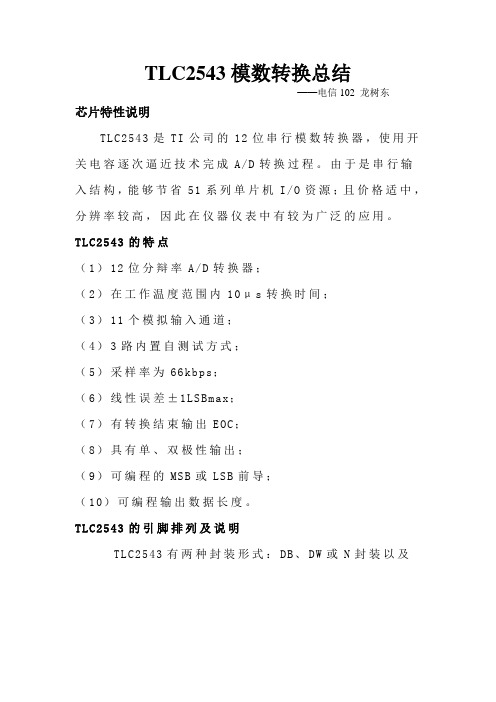
5.1硬件GMS90C××和GMS97C××系列是LGS公司的51系列单片机,这类单片机都不带SPI或相同的接口能力,为了和TLC2543模数转换器接口,需要用软件来模拟SPI的时序操作。
图4是TLC2543和GMS90C××或GMS97C××的接口简图,TLC2543的I/O时钟、数据输入、片选由并行双向I/O口1的引脚P1.0、P1.1、P1.3提供。
TLC2543的转换结果数据通过口1的P1.2脚接收,通道选择和方式数据通过口3输入到微控制器。
TLC2543QDWREP;TLC2543MDBREP;中文规格书,Datasheet资料

FEATURES(TOP VIEW)DW PACKAGE DESCRIPTION/ORDERING INFORMATION•Controlled Baseline•Programmable Power Down–One Assembly/Test Site,One Fabrication •Programmable Output Data Length Site•CMOS Technology•Extended Temperature Performance of –40°C •Application Report Available (2)to 125°C (TLC2543Q)and –55°C to 125°C (TLC2543M)•Enhanced Diminishing Manufacturing Sources (DMS)Support•Enhanced Product Change Notification •Qualification Pedigree (1)•12-Bit-Resolution Analog-to-Digital Converter (ADC)•10-µs Conversion Time Over Operating Temperature•11Analog Input Channels•Three Built-In Self-Test Modes•Inherent Sample-and-Hold Function •Linearity Error ...±1LSB Max •On-Chip System Clock•End-of-Conversion (EOC)Output•Unipolar or Bipolar Output Operation (Signed Binary With Respect to 1/2the Applied Voltage Reference)•Programmable Most Significant Bit (MSB)or Least Significant Bit (LSB)First(1)Component qualification in accordance with JEDEC and industry standards to ensure reliable operation over anextended temperature range.This includes,but is not limited to,Highly Accelerated Stress Test (HAST)or biased 85/85,temperature cycle,autoclave or unbiased HAST,electromigration,bond intermetallic life,and mold compound life.Such qualification testing should not be viewed as justifying use of this component beyond specified (2)Microcontroller Based Data Acquisition Using the TLC2543performance and environmental limits.12-bit Serial-Out ADC (SLAA012)The TLC2543is a 12-bit,switched-capacitor,successive-approximation,analog-to-digital converter (ADC).This device,with three control inputs [chip select (CS),input-output clock (I/O CLOCK),and address input (DATA INPUT)],is designed for communication with the serial port of a host processor or peripheral through a serial 3-state output.The device allows high-speed data transfers from the host.In addition to the high-speed converter and versatile control capability,the device has an on-chip 14-channel multiplexer that can select any 1of 11inputs or any 1of 3internal self-test voltages.The sample-and-hold function is automatic.At the end of conversion,the end-of-conversion (EOC)output goes high to indicate that conversion is complete.The converter incorporated in the device features differential high-impedance reference inputs that facilitate ratiometric conversion,scaling,and isolation of analog circuitry from logic and supply noise.A switched-capacitor design allows low-error conversion over the full operating temperature range.Please be aware that an important notice concerning availability,standard warranty,and use in critical applications of Texas Instruments semiconductor products and disclaimers thereto appears at the end of this data sheet.PRODUCTION DATA information is current as of publication date.Copyright ©2002–2006,Texas Instruments IncorporatedProducts conform to specifications per the terms of the Texas Instruments standard warranty.Production processing does not necessarily include testing of all parameters.DATA OUTDATA INPUT CSEOCAIN0AIN1AIN2AIN3AIN4AIN5AIN6AIN7AIN8AIN9AIN10SGLS125A–JULY 2002–REVISED NOVEMBER 2006ORDERING INFORMATIONT APACKAGE (1)ORDERABLE PART NUMBER TOP-SIDE MARKING –40°C to 125°C SOP –DW Tape and reel TLC2543QDWREP TLC2543QEP -55°C to 125°C SSOP -DBTape and ReelTLC2543MDBREPTLC2543MEP(1)Package drawings,standard packing quantities,thermal data,symbolization,and PCB design guidelines are available at /sc/package.FUNCTIONAL BLOCK DIAGRAM2Submit Documentation FeedbackTERMINAL FUNCTIONSTERMINALI/O DESCRIPTIONNAME NO.AIN01AIN12AIN23AIN34AIN45Analog input.These11analog-signal inputs are internally multiplexed.The driving sourceAIN56I impedance should be less than or equal to50Ωfor4.1-MHz I/O CLOCK operation,and be capable AIN67of slewing the analog input voltage into a capacitance of60pF.AIN78AIN89AIN911AIN1012Chip select.A high-to-low transition on CS resets the internal counters and controls and enablesCS15I DATA OUT,DATA INPUT,and I/O CLOCK.A low-to-high transition disables DATA INPUT and I/OCLOCK within a setup time.Serial-data input.A4-bit serial address selects the desired analog input or test voltage to beconverted next.The serial data is presented with the most significant bit(MSB)first and is shifted in DATA INPUT17Ion the first four rising edges of I/O CLOCK.After the four address bits are read into the addressregister,I/O CLOCK clocks the remaining bits in order.The3-state serial output for the A/D conversion result.DATA OUT is in the high-impedance statewhen CS is high and active when CS is low.With a valid CS,DATA OUT is removed from thehigh-impedance state and is driven to the logic level corresponding to the most significant bit/least DATA OUT16Osignificant bit(MSB/LSB)value of the previous conversion result.The next falling edge of I/OCLOCK drives DATA OUT to the logic level corresponding to the next MSB/LSB,and the remainingbits are shifted out in order.End of conversion.EOC goes from a high to a low logic level after the falling edge of the last I/O EOC19OCLOCK and remains low until the conversion is complete and the data is ready for transfer.Ground.GND is the ground return terminal for the internal circuitry.Unless otherwise noted,allGND10voltage measurements are with respect to GND.Input/output clock.I/O CLOCK receives the serial input and performs the following four functions:•It clocks the eight input data bits into the input data register on the first eight rising edges of I/OCLOCK with the multiplexer address available after the fourth rising edge.•On the fourth falling edge of I/O CLOCK,the analog input voltage on the selected multiplexer inputbegins charging the capacitor array and continues to do so until the last falling edge of the I/OI/O CLOCK18ICLOCK.•It shifts the11remaining bits of the previous conversion data out on DATA OUT.Data changes onthe falling edge of I/O CLOCK.•It transfers control of the conversion to the internal state controller on the falling edge of the lastI/O CLOCK.Positive reference voltage.The upper reference voltage value(nominally V CC)is applied to REF+. REF+14I The maximum input voltage range is determined by the difference between the voltage applied tothis terminal and the voltage applied to the REF–terminal.Negative reference voltage.The lower reference voltage value(nominally ground)is applied toREF–13IREF–.V CC20Positive supply voltage3Submit Documentation FeedbackAbsolute Maximum Ratings (1)Recommended Operating ConditionsSGLS125A–JULY 2002–REVISED NOVEMBER 2006over operating free-air temperature range (unless otherwise noted)MINMAX UNIT V CC Supply voltage range (2)–0.5 6.5V V CC +V I Input voltage range (any input)–0.3V 0.3V CC +V O Output voltage range –0.3V 0.3V CC +V ref+Positive reference voltage V 0.1V ref–Negative reference voltage –0.1V I I Peak input current (any input)±20mA I I Peak total input current (all inputs)±30mA TLC2543Q –40125T A Operating free-air temperature range °C TLC2543M-55125T stg Storage temperature range–65150°C Lead temperature 1,6mm (1/16in)from the case for 10s260°C(1)Stresses beyond those listed under "absolute maximum ratings"may cause permanent damage to the device.These are stress ratings only,and functional operation of the device at these or any other conditions beyond those indicated under "recommended operating conditions"is not implied.Exposure to absolute-maximum-rated conditions for extended periods may affect device reliability.(2)All voltage values are with respect to the GND terminal with REF–and GND wired together (unless otherwise noted).(1)Analog input voltages greater than that applied to REF+convert as all ones (111111111111),while input voltages less than that applied to REF–convert as all zeros (000000000000).(2)To minimize errors caused by noise at the CS input,the internal circuitry waits for a setup time after CS ↓before responding to control input signals.No attempt should be made to clock in an address until the minimum CS setup time has elapsed.(3)This is the time required for the clock input signal to fall from V IH min to V IL max or to rise from V IL max to V IH min.In the vicinity of normal room temperature,the devices function with input clock transition time as slow as 1µs for remote data acquisition applications where the sensor and the ADC are placed several feet away from the controlling microprocessor.4Submit Documentation FeedbackElectrical Characteristicsover recommended operating free-air temperature range,VCC =Vref+=4.5V to5.5V,f(I/O CLOCK)=4.1MHz(unless otherwise noted)PARAMETER TEST CONDITIONS MIN TYP(1)MAX UNITV CC=4.5V,I OH=–1.6mA 2.4V OH High-level output voltage VV CC=4.5V to5.5V,I OH=–20µA V CC–0.1V CC=4.5V,I OL=1.6mA0.4V OL Low-level output voltage VV CC=4.5V to5.5V,I OL=20µA0.1V O=V CC,CS at V CC1 2.5 High-impedance off-stateI OZµAoutput current VO=0,CS at V CC1–2.5I IH High-level input current V I=V CC110µAI IL Low-level input current V I=01–10µAI CC Operating supply current CS at0V1 2.5mAFor all digital inputs,I CC(PD)Power-down current425µA0≤V I≤0.5V or V I≥V CC–0.5VSelected channel at V CC,Unselected channel at0V10 Selected channelµA leakage current Selected channel at0V,Unselected channel at VCC–10Maximum static analogV ref+=V CC,V ref–=GND1 2.5µA reference current into REF+Analog inputs3060 InputC i pFcapacitance Control inputs515(1)All typical values are at V CC=5V,T A=25°C.5Submit Documentation FeedbackOperating CharacteristicsSGLS125A–JULY2002–REVISED NOVEMBER2006over recommended operating free-air temperature range,VCC =Vref+=4.5V to5.5V,f(I/O CLOCK)=4.1MHz(1)All typical values are at T A=25°C.(2)Linearity error is the maximum deviation from the best straight line through the A/D transfer characteristics.(3)Gain error is the difference between the actual midstep value and the nominal midstep value in the transfer diagram at the specified gainpoint after the offset error has been adjusted to zero.Offset error is the difference between the actual midstep value and the nominal midstep value at the offset point.(4)Analog input voltages greater than that applied to REF+convert as all ones(111111111111),while input voltages less than that appliedto REF–convert as all zeros(000000000000).(5)Total unadjusted error comprises linearity,zero-scale,and full-scale errors.(6)Both the input address and the output codes are expressed in positive logic.(7)I/O CLOCK period=1/(I/O CLOCK frequency)(see Figure7)(8)Any transitions of CS are recognized as valid only is maintained for a setup time.CS must be taken low at≤5µs of thetenth I/O CLOCK falling edge to ensure a conversion is aborted.Between5µs and10µs,the result is uncertain as to whether the conversion is aborted or the conversion results are valid.6Submit Documentation FeedbackPARAMETER MEASUREMENT INFORMATIONC110 µF−15 VVC110 µFLOCATIONU1C1C2C3DESCRIPTIONOP2710-µF 35-V tantalum capacitor0.1-µF ceramic NPO SMD capacitor470-pF porcelain Hi-Q SMD capacitorPART NUMBER——AVX 12105C104KA105 or equivalentJohanson 201S420471JG4L or equivalentEOCC LVR L = 2.18 kΩC LVR L = 2.18 kΩCSDATAOUTtI/O CLOCKFigure1.Analog Input Buffer to Analog Inputs AIN0–AIN10Figure2.Load CircuitsFigure3.DATA OUT to Hi-Z Voltage Waveforms Figure4.DATA INPUT and I/O CLOCKVoltage Waveforms7Submit Documentation FeedbackCSI/O CLOCKI/O CLOCKDATA OUTt t EOCDATA OUTSGLS125A–JULY 2002–REVISED NOVEMBER 2006A.To ensure full conversion accuracy,it is recommended that no input signal change occurs while a conversion is ongoing.Figure 5.CS and I/O CLOCK Voltage WaveformsFigure 6.I/O CLOCK and DATA OUT Voltage WaveformsFigure 7.I/O CLOCK and EOC Voltage WaveformsFigure 8.EOC and DATA OUT Voltage Waveforms8Submit Documentation FeedbackA.To minimize errors caused by noise at CS,the internal circuitry waits for a setup time after CS ↓before responding to control input signals.Therefore,no attempt should be made to clock in an address until the minimum CS setup time has elapsed.Figure 9.Timing for 12-Clock Transfer Using CS With MSB FirstA.To minimize errors caused by noise at CS,the internal circuitry waits for a setup time after CS ↓before responding to control input signals.Therefore,no attempt should be made to clock in an address until the minimum CS setup time has elapsed.Figure 10.Timing for 12-Clock Transfer Not Using CS With MSB First9Submit Documentation FeedbackI/O CLOCKDATA OUT DATA INPUTCSEOCSGLS125A–JULY 2002–REVISED NOVEMBER 2006A.To minimize errors caused by noise at CS,the internal circuitry waits for a setup time after CS ↓before responding to control input signals.Therefore,no attempt should be made to clock in an address until the minimum CS setup time has elapsed.Figure 11.Timing for 8-Clock Transfer Using CS With MSB FirstA.To minimize errors caused by noise at CS,the internal circuitry waits for a setup time after CS ↓before responding to control input signals.Therefore,no attempt should be made to clock in an address until the minimum CS setup time has elapsed.Figure 12.Timing for 8-Clock Transfer Not Using CS With MSB First10Submit Documentation Feedback分销商库存信息:TITLC2543QDWREP TLC2543MDBREP。
TLC2543中文数据手册

TLC2543使用手册一、简要说明:TLC2543是一款8位、10位、12位为一体的可选输出位数的11通道串行转换芯片。
每一路转换时间为10us。
外部输入信号为:DATA input ;_CS;AD_IO_CLK;Analog input;四种信号;输出为:EOC转换结束信号,DATA output信号。
工作原理为:_CS由高变为低时候,允许DATA input;AD_IO_CLK;Analog input信号输入,DATA out 信号输出;由低到高禁止DATA input;AD_IO_CLK;信号输入。
当忽略ADC转换启动的CS时候,数据的输出是在CS的下降沿,既是将片选的时候,而考虑到CS时候,第一个输出数据发生在EOC变为高的时候的上升沿。
注意:初始化时候,必须将CS由高拉低才能进行数据输出或者是数据输入。
也就是说,当一次转换完成后,进行下一次或者是下一个通道的转换,需要将CS由低拉高,为下一次转换做好准备,当进行下一个转换时候,进行CS 拉低,DATA input输入或者DATA out输出(忽略CS转换作用时候)。
信号解释:DATA input:4位串行地址输入,用来选择模拟输入通道功能或者测试引脚;高位在前,在每一个AD_IO_CLK的上升沿输入ADC的寄存器。
由八位组成:前四位:D7:D4用作选择模拟输入通道,D3:D2用作选择数据长度,D1是选择输出高低位顺序的,D0选择是选择输出极性(单双极性)。
DA TA INPUT的表含义DATA OUT:当_CS为高时DATA out输出为高阻抗,当CS有效时,驱动转换结果,并在AD_IO_CLK的下降沿按位顺序输出。
EOC:ADC的EOC在DATA input输入的最后一个AD_IO_CLK时,由高变为低,并保持到转换结束和数据准备输出结束时候变为高。
AD_IO_CLK:输入和输出时钟,主要完成以下功能:A、在IO_CLK的前八个时钟的上升沿将DATA input的八位数据输入数据寄存器中。
12位TLC2543模数转换总结
Lcd_wcd(1,0x2e);
Lcd_wcd(1,0x30+shi);
Lcd_wcd(1,0x30+ge);
Lcd_wcd(1,0x30+xiao);
/*for(i=0;i<SUM;i++)
{
temp1+=redad(0x01);//选择通道1,并读取AD转换的数
GND
地。GND是内部电路的地回路端。除另有说明外,所有电压测量都相对GND而言
18
I/O CLOCK
I
输入/输出时钟端。I/OCLOCK接收串行输入信号并完成以下四个功能:(1)在I/O CLOCK的前8个上升沿,8位输入数据存入输入数据寄存器。(2)在I/OCLOCK的第4个下降沿,被选通的模拟输入电压开始向电容器充电,直到I/OCLOCK的最后一个下降沿为止。(3)将前一次转换数据的其余11位输出到DATA OUT端,在I/OCLOCK的下降沿时数据开始变化。(4)I/OCLOCK的最后一个下降沿,将转换的控制信号传送到内部状态控制位
//uchar code dis1[]={"采集电压:000 v"};
/*************延时**************/
void delay(uint z)
{//一毫秒
uint y;
for(;z>0;z--)
for(y=110;y>0;y--) ;
}
void delay_us(uchar n)//微秒
shi=x/1000%10;
ge=x/100%10;
xiao=x/10%10;
}
/****************主函数****************/
TLC2543中文资料

串行A D转换器T L C2543中文资料T L C2543是T I公司的12位串行模数转换器,使用开关电容逐次逼近技术完成A/D转换过程。
由于是串行输入结构,能够节省51系列单片机I/O资源;且价格适中,分辨率较高,因此在仪器仪表中有较为广泛的应用。
2T L C2543的特点(1)12位分辩率A/D转换器;(2)在工作温度范围内10μs转换时间;(3)11个模拟输入通道;(4)3路内置自测试方式;(5)采样率为66k b p s;(6)线性误差±1L S B m a x;(7)有转换结束输出E O C;(8)具有单、双极性输出;(9)可编程的M S B或L S B前导;(10)可编程输出数据长度。
3T L C2543的引脚排列及说明T L C2543有两种封装形式:D B、D W或N封装以及F N封装,这两种封装的引脚排列如图1,引脚说明见表1。
图1T L C2543的封装4接口时序可以用四种传输方法使T L C2543得到全12位分辩率,每次转换和数据传递可以使用12或16个时钟周期。
一个片选()脉冲要插到每次转换的开始处,或是在转换时序的开始处变化一次后保持为低,直到时序结束。
图2显示每次转换和数据传递使用16个时钟周期和在每次传递周期之间插入的时序,图3显示每次转换和数据传递使用16个时钟周期,仅在每次转换序列开始处插入一次时序。
引脚号名称I/O说明1~9,11,12AIN0~AIN10I模拟量输入端。
11路输入信号由内部多路器选通。
对于4.1MHz的I/OCLOCK,驱动源阻抗必须小于或等于50Ω,而且用60pF电容来限制模拟输入电压的斜率15I片选端。
在端由高变低时,内部计数器复位。
由低变高时,在设定时间内禁止DATAINPUT和I/O CLOCK17DATAINPUT I串行数据输入端。
由4位的串行地址输入来选择模拟量输入通道16DATA OUT O A/D转换结果的三态串行输出端。
- 1、下载文档前请自行甄别文档内容的完整性,平台不提供额外的编辑、内容补充、找答案等附加服务。
- 2、"仅部分预览"的文档,不可在线预览部分如存在完整性等问题,可反馈申请退款(可完整预览的文档不适用该条件!)。
- 3、如文档侵犯您的权益,请联系客服反馈,我们会尽快为您处理(人工客服工作时间:9:00-18:30)。
摘要介绍TI公司的TLC2543的特性,与51系列单片机的接口以及在仪器仪表中的应用。
关键词串行A/D应用
1引言
TLC2543是TI公司的12位串行模数转换器,使用开关电容逐次逼近技术完成A/D转换过程。
由于是串行输入结构,能够节省51系列单片机I/O资源;且价格适中,分辨率较高,因此在仪器仪表中有较为广泛的应用。
2TLC2543的特点
(1)12位分辩率A/D转换器;
(2)在工作温度范围内10μs转换时间;
(3)11个模拟输入通道;
(4)3路内置自测试方式;
(5)采样率为66kbps;
(6)线性误差±1LSBmax;
(7)有转换结束输出EOC;
(8)具有单、双极性输出;
(9)可编程的MSB或LSB前导;
(10)可编程输出数据长度。
3TLC2543的引脚排列及说明
TLC2543有两种封装形式:DB、DW或N封装以及FN封装,这两种封装的引脚排列如图1,引脚说明见表1。
图1TLC2543的封装
i
表1TLC2543引脚说明
4接口时序
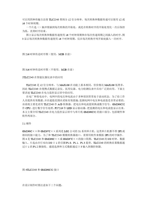
可以用四种传输方法使TLC2543得到全12位分辩率,每次转换和数据传递可以使用12或16个时钟周期。
一个片选()脉冲要插到每次转换的开始处,或是在转换时序的开始处变化一次后保持为低,直到时序结束。
图2显示每次转换和数据传递使用16个时钟周期和在每次传递周期之间插入的时序,图3显示每次转换和数据传递使用16个时钟周期,仅在每次转换序列开始处插入一次时序。
图216时钟传送时序图(使用,MSB在前)
图316时钟传送时序图(不使用,MSB在前)
5TLC2543在智能仪器仪表中的应用
TLC2543是12位分辩率,与MAX186在功能上基本相同,但价格比MAX186低得多,因此TLC2543在便携式数据记录仪、医用仪器、电力检测仪表中具有广泛的应用。
下面主要讲述TLC2543在电力监控显示屏中的应用。
在电厂和变电站中,电网中的电压和电流由于多种原因常常处于波动状态,为了给工作人员提供有效数据,并在超值范围内采取有效措施,监测电网中电压和电流值是非常必要的。
该系统主要是采用TLC2543作
A/D转换器,把电压和电流值转换成数字信号,GMS90C32作CPU,进行数字信号处理,PS7219作LED 显示驱动器,把监测的电压和电流值显示出来,本文主要介绍TLC2543在电力监控显示屏中与单片机GMS90C32的接口部分,包括硬件和软件两部分。
5.1硬件
GMS90C××和GMS97C××系列是LGS公司的51系列单片机,这类单片机都不带SPI或相同的接口能力,为了和TLC2543模数转换器接口,需要用软件来模拟SPI的时序操作。
图4是TLC2543和GMS90C××或GMS97C××的接口简图,TLC2543的I/O时钟、数据输入、片选由并行双向I/O口1的引脚P1.0、P1.1、P1.3提供。
TLC2543的转换结果数据通过口1的P1.2脚接收,通道选择和方式数据通过口3输入到微控制器。
图4TLC2543和GMS90C32接口
在设计制作时要注意如下
三个问题:
(1)电源去耦
当使用TLC2543这种12位A/D器件时,每个模拟IC的电源端必须用一个0.1μF的陶瓷电容连接到地,用作去耦电容。
在噪声影响较大的环境中,建议每个电源和陶瓷电容端并一个10μF的钽电容,这样能够减小噪声的影响。
(2)接地
对模拟器件和数字器件,电源的地线回路必须分开,以防止数字部分的噪声电流通过模拟地回路引入,产生噪声电压,从而对模拟信号产生干扰。
所有的地线回路都有一定的阻抗,因此地线要尽可能宽或用地线平面,以减小阻抗,连线应当尽可能短,如果使用开关电源,则开关电源要远离模拟器件。
(3)电路板布线
使用TLC2543时一定要注意电路板的布线,电路板的布线要确保数字信号和模拟信号隔开,模拟线和数字线特别是时钟信号线不能互相平行,也不能在TLC2543芯片下面布数字信号线。
5.2软件
包括主程序和两个子程序“SET1”、“SET2”。
主程序定义口1的I/O引脚方向:P1.2设置为输入端,P1.0、P1.1和P1.3设置为输出端。
设定P1.3使TLC2543片选端为高,“SET1”被调用,这个子程序模拟SPI操作,在TLC2543和微控制器间交换数据。
检测最低位前导(LSBF)标志,即通道选择/方式数据字节的位1,以决定转换结果的哪个字节最先传送,子程序“SET2”用于映射相应于所选择的特定通道的MSBYTE和LSBYTE到偶数或奇数的RAM地址。
程序清单如下:
ORG2000H
BEGIN:MOVSP,#50H;设置堆栈指针
MOVP1,#04H;定义口1的输入和输出
CLRP1.0;清I/O时钟
SETBP1.3;设置片选
为高
MOVA,#0FFH
ACALLSET1;调SET1子程序
ACALLSET2;调SET2子程序
JMPBEGIN;转到BEGIN
SET1:MOVR4,P3;读方式/通道数据
MOVA,R4
CLRP1.3;设置片选为低
JBACC.1,LSB;如果A的位1为1,则先传送低字节
MSB:MOVR5,#08H;设置高4位计数器
LOP1:MOVC,P1.2;读转换结果
RLCA;A寄存器的内容左移
MOVP1.1,C;输出方式/通道字节
SETBP1.0;设置I/O时钟为高
CLRP1.0;设置I/O时钟为低
DJNZR5,LOP1;不为0则返回LOP1
MOVR2,A;把高字节放到R2
MOVA,R4;把方式/通道控制字放到R2
JBACC.1,RETURN
LSB:MOVR5,#08H;设置低字节计数器
LOP2:MOVC,P1.2;读转换数据到C
RLCA;A的内容到C
MOVP1.1,C;输出方式/通道字节
SETBP1.0;设置时钟为高
CLRP1.0;设置时钟为低
DJNZR5,LOP2;R5不为0,则返回LOP2
MOVR3,A;把低字节反放到R3
MOVA,R4;把方式/通道控制字放到R3
JBACC.1,MSB;如果R4的位1为1,则传送高字节RETURN:RET
SET2:MOVA,R4;读方式/通道控制字
ANLA,#0F0H;保留通道控制字
SWAPA;A寄存器中的高4和低4位交换
MOVB,#02H
MULA,B;A和B相乘
ADDA,#030H;A的内容再加30H
MOVR1,A
MOVA,R2
MOV@R1,A;把高字节的内容放到对应地址中
INCR1
MOVA,R3
MOV@R1,A;把低字节的内容放到对应地址中
RET
END。