UV整流器规格书
整流桥说明书
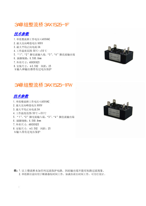
9.输入带有过电压保护9.输入和输出都带有过电压保护
:
技术参数
1.单组整流桥工作电压≤400VAC
2.最大反向峰值电压900V
3.最大平均正向电流3A
4.工作温度范围-50℃~+50℃
5.“1”、“2”脚交流输入端,“3”、“4”脚直流输出端
6.插脚规格:6.5X0.8mm
7.外形尺寸:48X30X25
8.安装尺寸:φ3.5X2 间距:25
注:1.
2.单组桥目前应用于断路器短时间工作,如满负荷长时间工作,可另行设计。
技术参数1.单组整流桥工作电压≤400VAC
2.最大反向峰值电压900V
3.最大平均正向电流3A
4.工作温度范围-50℃~+50℃
5.“1”
、“2”脚交流输入端,“3”、“4”脚直流输出端6.插脚规格:6.5X0.8mm
7.外形尺寸:48X30X25
8.安装尺寸:φ3.5X2 间距:25
3A单组整流桥3AX1525-1F
3A单组整流桥3AX1525-1FW
以上整流桥未加任何过流保护电路,因此输出端不能有短路过流现象。
ZXD5000(V2.0)100A开关整流器用户手册

第二章 工作原理及结构 ...............................................................................................................................3 2.1 开关整流器工作原理........................................................................................................................3 2.2 结构介绍............................................................................................................................................4
sv01-003规格书
sv01-003规格书SV01-003规格书是一份详细描述产品规格和特性的文件,对于制造商和消费者来说至关重要。
本文将详细介绍SV01-003规格书的内容,包括产品描述、技术规格、性能特点等,以帮助读者更好地了解该产品。
一、产品描述SV01-003是一款高性能电子产品,主要用于xxx领域。
该产品采用先进的技术和工艺,具有优良的性能和稳定的品质,广泛应用于xxx 等领域。
二、技术规格1.外形尺寸:xxmm2.重量:xxxg3.颜色:xxx4.包装:xxx5.材质:xxx6.工作温度:-xx℃~xx℃7.存储温度:-xx℃~xx℃8.输入电压:xxxV9.输出电压:xxxV10.频率范围:xxxHz三、性能特点1.高性能处理器,提供快速响应速度。
2.大容量存储空间,可存储大量数据。
3.高清晰屏幕,显示效果清晰。
4.多种接口,适配多种设备。
5.高保密性,信息安全性高。
6.长续航时间,使用时间长久。
四、功能特点1.支持多种格式文件的读写。
2.支持蓝牙、WIFI等无线连接。
3.支持摄像功能,拍照清晰。
4.支持多任务操作,提高工作效率。
5.支持语音识别功能,便捷操作。
6.支持智能控制功能,自动化操作。
五、安全性能1.支持密码锁功能,保护隐私安全。
2.支持指纹识别功能,提高安全性。
3.支持远程定位功能,防盗追踪。
六、使用方法1.在使用前,请仔细阅读说明书。
2.开机前请充电,保证电量充足。
3.操作前请确认设备连接正常。
4.操作时请保持设备干燥,防止进水。
5.结束使用后请及时关闭设备,节约电量。
七、维护保养1.定期清洁设备表面,保持外观清洁。
2.避免硬物划伤设备表面。
3.避免长时间曝晒在阳光下。
4.注意防尘,定期清理设备内部。
八、包装信息1.包装规格:xxx2.包装材质:xxx3.包装方式:xxx4.包装清单:xxx以上就是SV01-003规格书的主要内容,希望通过本文的介绍,读者对该产品有更详细的了解和认识。
SV01-003作为一款高性能电子产品,具有很多先进的技术和功能,能够满足广泛的使用需求,是xxx行业的优选产品。
LP12A规格书
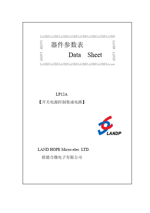
图4. (1)上电 (2)正常工作 (3)自动重启 (4)电源关断时的典型波形
脉宽调制器 脉宽调制器通过驱动输出MOSFET来实现多模式控制,其占空比与流入控制脚超过芯片内部消 耗所需要的电流成反比(如图3)。反馈误差信号以过电流的形式, 由一个典型转折频率为 7 kHz的RC滤波电路进行滤波,以降低芯片电源电流中由MOSFET栅极驱动产生的开关噪音。 要优化电源效率,需要实施四个不同的控制模式。在最大负载条件下,调制器将在全频PWM 模式下进行工作,随着负载的增加,调制器将自动依次切换到变频PWM模式和低频PWM模式。 在轻负载条件下,控制方式将从PWM控制切换到多周期调制控制,调制器在多周期调制模式 下进行工作。虽然不同模式的工作方式有所不同,但为了实现模式间的平滑切换,图3中所
振荡器和开关频率 内部振荡器使内部电容在两个设定的电压值间线性充放电,以产生脉宽调制解调器所需的三 角波电压。在每个周期的起点,振荡器将脉宽调制解调器/电流限制的触发器电路置位。全 开关频率选择为66kHz。全频PWM模式下,66kHz开关频率大约在±2.5kHz的范围内以250Hz 的速率抖动。当系统进入固定漏极峰值电流的变频模式后,频率抖动将关闭。
图 2. 内部结构框图
引脚功能描述
管脚 1
5,6,7,8 3 4 2
符号 S D C NC M
管脚定义描述 功率管的源极 功率管的漏极 控制反馈引脚 空脚,不连接 多功能引脚
控制(C)引脚: 误差放大器及反馈电流的输入脚,用于占空比控制。与内部并联调整器相连接,提供正常工 作时的内部偏置电流。也用作电源旁路和自动重启动/补偿电容的连接点。 漏极(D)引脚: 高压功率MOSFET漏极引脚。通过内部的开关高压电流源提供启动偏置电流。 源极(S)引脚: 这个引脚是功率MOSFET的源极连接点,用于高压功率的回路。它也是控制反馈脚的参考地。 空脚(NC)引脚: 该脚为空脚,与芯片内部无连接,外部应用无需连接。 多功能(M)引脚: 是过压(OV)、欠压(UV)、降低DCMAX的线电压前馈、输出过压保护(OVP)、外部流限调节、远 程开/关和器件重置的输入引脚。多功能引脚组合了电压监测及外部流限引脚功能。但其中 某些功能不能同时实现。连接至源极则禁用此引脚的所有功能实现简单的三端模式工作。
杰生电气深紫外LED产品统一的规格书
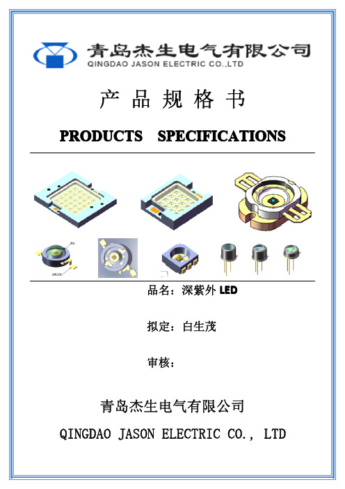
产品规格书PRODUCTS SPECIFICATION SPECIFICATIONSS品名:深紫外LED 拟定:白生茂审核:青岛杰生电气有限公司QINGDAO JASON ELECTRIC CO.,LTD—————————————————————————图1产品外观俯视图图2产品外观纵切图3、光学-电学参数:(T A=15℃;I F=20mA)项目单位参考值参考电压(V F)V 6.5图3相对光谱分布图4相对光强随角度分布5、电学特性:(T A=15℃;I F=20mA)图5辐射功率百分比随电流变化特性图6I-V特性6、使用注意事项及其他:○1不要触及LED正面,以免影响器件正常发光;○2接通电源器件前必须确认正负极,反接会损坏器件;○3参考电压6.5V;电压范围0~10V;电压过高点亮可能会损坏器件;○4不要直接用肉眼近距离观察发光情况;青岛杰生电气有限公司1产品外观俯视图图2产品外观纵切图电学参数:(T A=15℃项目参考值参考电压(V F) 6.5工作电流(I F)20峰值波长(λP)280半高宽(FWHM)10发光角度(θ)60青岛杰生电气有限公司图3相对光谱分布图4相对光强随角度分布5、电学特性:(T A=15℃;I F=20mA)图5辐射功率百分比随电流变化特性图6I-V特性6、使用注意事项及其他:○1不要触及LED正面,以免影响器件正常发光;○2接通电源器件前必须确认正负极,反接会损坏器件;○3参考电压6.5V;电压范围0~10V;电压过高点亮可能会损坏器件;○4不要直接用肉眼近距离观察发光情况;青岛杰生电气有限公司图1TO39-Low-Flat图3相对光谱分布图4相对光强随角度分布5、电学特性:(T A=15℃;I F=20mA)图5辐射功率百分比随电流变化特性图6I-V特性6、使用注意事项及其他:○1不要触及LED正面,以免影响器件正常发光;○2接通电源器件前必须确认正负极,反接会损坏器件;○3参考电压6.5V;电压范围0~10V;电压过高点亮可能会损坏器件;○4不要直接用肉眼近距离观察发光情况;青岛杰生电气有限公司—————————————————————————————————附录。
整流器的UL935标准
第1部分—所有产品绪论1.范围1.1 本标准的要求,适用于荧光灯用的电阻、电抗和电子(固态)型镇流器,其电压包括按国家电气规范NFPA70所规定的2500V及以下之规格。
1.2荧光灯镇流器可以在固定装置或其它装置上,用荧光灯以外的放电灯来审核确定其是否适用。
1.3 对于UL 1993——自镇流灯和灯的转接器,使用标准评估荧光自镇流器和镇流器镇流器。
1.4包含有性能、特性、元件、材料或当标准发展后,在使用上就成为新的或有差别的系统上的产品,以及包括那些有着火、触电或对人体伤害危险的产品,须用相应附件经贸终端产品的要求进行评价,来确定必需保持的由本标准原来所预期的对产品使用权用者的安全水平。
2.术语2.1下列定义适用于本标准。
2.2 镇流器——利用电抗或电阻,以单个或组合的方式,为了适当的工作而限制灯管电流至规定值,并且,如有需要,提供足够的启动电压的装置。
此外,对于快速启动线路的场合,还提供用于低压灯丝加热的装置。
2.3 粗棉布——在异常条件试验中,将其作为一火灾指示器来使用。
粗棉布大约36英寸(910mm)宽,转动率大约14-15码/磅(28-30m/kg),对于任何平方英寸,其在一个方向有32个螺纹,另一个方向上有28个螺纹(对于任何平方厘米,一个方向为13个螺纹而另一个方向为11个螺纹)。
2.4 P类的保护镇流器——带有防异常热的镇流器,其镇流器和保护集合成一整体部分且符合本标准的要求。
2.5 小型荧光灯——所有接线触头集中在承担全部机械支承作用的单个底座上的一种外型细小(例如折叠结构)的一种荧光灯。
2.6 处理过的灯管——至少经过100h工作的新灯管。
2.7 普通磁性镇流器——由电线线圈组成的镇流器。
电线线芯和操作在电源网络频率下。
普通带磁性的镇流器为变压器型或一般电抗型。
带磁性的镇流器一般带有功率电容。
2.8 不激活灯管——由于灯丝发射物质耗尽,因而灯管不能被电离而造成寿命终结的灯管。
2.9 电子镇流器——一种受有源元件(晶体管、可控硅及类似元件)控制的高频转换装置的,并且由串联容抗或感抗与灯一起,为适应高的转换频率而提供稳定阻抗的一种镇流器。
一种新的电压型PWM整流器无源控制器设计_王久和

式(18)第 3 个式子满足功率平衡,稳态时 udc 的 稳态值等于给定值 udcr。
式 (18) 表 明 控 制 律 式 (15) 可 实 现 系 统 动 态 和 静
态解耦,提高系统的动、静态性能。
2.3 仿真实验
仿真参数:电源相电压 220 V, f = 50 Hz,电感 L =
16 mH,电 阻 R = 0.3 Ω,C = 2 200 μF,额 定 负 载 RL = 100 Ω。 调制频率 5 kHz。 udcr = 600 V。 Im 按式(9)计 算。 仿真用 Simulink 中 SimPowerSystems 模块实现。
200 Ω 的点,D 为负载从 200 Ω 变为 100 Ω 的点。 在
Ra=10 Ω、50 Ω、100 Ω 时整流器的性能见表 1。
(10)
取误差能量函数
V
=
x
T e
M
xe
/
2
(11)
为使系统快速收敛到期望点,使式 (11)快 速 变
零,需要注入阻尼,加速系统能量耗散。 注入阻尼耗
散项为
R Dxe = ( R + Ra)xe
(12)
式中 Ra 为正定矩阵。 方程式(10)可变为
M x觶e + R D xe = u - [M x觶* + J(x* + xe) +
摘要: 为克服现行电压型 PWM 整流器无源控制器存在的缺点(如负载变化、电源不平衡时存在较
大的直流电压稳态误差,系统的响应速度不理想等),基于整流器在两相同步旋转 dq 坐标系中的
欧拉 - 拉格朗日 EL(Euler 鄄Lagrange)数学模型和无源性,通过阻尼注入方法,提出了一种由状态期
STPS20M100S Power Schottky整流器规格书说明书
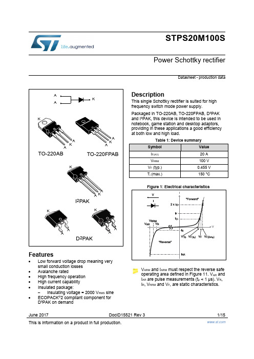
June 2017 DocID15521 Rev 3 1/15This is information on a product in full production.STPS20M100SPower Schottky rectifierDatasheet - production dataFeatures∙ Low forward voltage drop meaning very small conduction losses ∙Avalanche rated∙ High frequency operation ∙ High current capability ∙ Insulated package:- Insulating voltage = 2000 V RMS sine ∙ECOPACK ®2 compliant component for D²PAK on demandDescriptionThis single Schottky rectifier is suited for high frequency switch mode power supply.Packaged in TO-220AB, TO-220FPAB, D²PAK and I²PAK, this device is intended to be used in notebook, game station and desktop adaptors, providing in these applications a good efficiency at both low and high load.Figure 1: Electrical characteristicsV ARM and I ARM must respect the reverse safe operating area defined in Figure 11. V AR and I AR are pulse measurements (t p < 1 μs). V R , I R , V RRM and V F , are static characteristics.Characteristics STPS20M100S1 CharacteristicsTable 2: Absolute ratings (limiting values with terminals 1 and 3 short circuited, at 25 °CNotes:(1)For pulse time duration deratings, refer to Figure 4 . More details regarding the avalanche energymeasurements and diode validation in the avalanche are provided in the application notes AN1768 and AN2025.(2)Refer to Figure 11(3)(dP tot/dT j) < (1/R th(j-a)) condition to avoid thermal runaway for a diode on its own heatsink.STPS20M100S CharacteristicsNotes:(1)Pulse test: t p= 5 ms, δ < 2%(2)Pulse test: t p= 380 µs, δ < 2%To evaluate the conduction losses, use the following equation:P = 0.425 x I F(AV) + 0.0088 x I F2(RMS)Characteristics STPS20M100S 1.1 Characteristics (curves)Package information STPS20M100S2 Package informationIn order to meet environmental requirements, ST offers these devices in different grades ofECOPACK® packages, depending on their level of environmental compliance. ECOPACK®specifications, grade definitions and product status are available at: .ECOPACK® is an ST trademark.∙Cooling method: by conduction (C)∙Epoxy meets UL 94,V0∙Recommended torque value: 0.55 N·m (for TO-220AB and TO-220FPAB)∙Maximum torque value: 0.7 N·m (for TO-220AB and TO-220FPAB)2.1 TO-220AB package informationSTPS20M100S Package informationPackage information STPS20M100S 2.2 TO-220FPAB package informationSTPS20M100S Package informationPackage information STPS20M100S 2.3 I²PAK package informationSTPS20M100SPackage information2.4 D²PAK package informationThis package drawing may slightly differ from the physical package. However, all the specified dimensions are guaranteed.Package information STPS20M100SSTPS20M100S Package informationFigure 16: D²PAK recommended footprint (dimensions in mm)Ordering information STPS20M100S 3 Ordering information4 Revision historySTPS20M100SIMPORTANT NOTICE – PLEASE READ CAREFULLYSTMicroelectronics NV and its subsidiaries (“ST”) reserve the right to make changes, corrections, enhancements, modifications, and improvements to ST products and/or to this document at any time without notice. Purchasers should obtain the latest relevant information on ST products before placing orders. ST products are sold pursuant to ST’s terms and conditions of sale in place at the time of or der acknowledgement.Purchasers are solely responsible for the choice, selection, and use of ST products and ST assumes no liability for application assistance or the design of Purchasers’ products.No license, express or implied, to any intellectual property right is granted by ST herein.Resale of ST products with provisions different from the information set forth herein shall void any warranty granted by ST for such product.ST and the ST logo are trademarks of ST. All other product or service names are the property of their respective owners.Information in this document supersedes and replaces information previously supplied in any prior versions of this document.© 2017 STMicroelectronics – All rights reserved。
整流器技术规格书

供电系统整流器技术规格书2009年6月目录1.总则 (2)1.1本文件适用范围 (2)1.2供货范围内设备类型 (2)2.工程概况 (2)2.1工程说明 (2)2.2环境条件 (2)2.3系统运行方式 (2)2.4相关系统和设备参数 (3)3.设备数量 (4)4.主要元器件清单 (5)5.备品备件、测试工具 (5)6.整流器技术要求 (6)6.1采用标准 (6)6.2技术规格及要求 (7)6.3结构要求 (9)6.4设备的互换性 (10)6.5铭牌 (10)6.6试验内容 (10)6.7接口 (11)7.设备其它要求 (12)7.1工艺要求和防锈 (12)7.2可靠性、可维护性、电磁辐射及兼容 (12)7.3柜体的颜色 (13)7.4标示 (13)1.总则1.1 本文件适用范围本文件适用于北京地铁15号线一期工程整流器设备供货,并作为供应商供货设备的技术依据。
1.2 供货范围内设备类型整流器柜、备品备件和专用工具。
2.工程概况2.1 工程说明北京地铁15号线位于北京东北部地区,主要分布在海淀、朝阳、顺义三个行政区。
线路起点位于西苑,沿颐和园路、清华西路下穿地铁4号线、穿过清华大学,沿清华东路向东,穿过八达岭高速公路,至奥林匹克中心区,沿大屯路继续向东至鼎成路转向南,穿过京承高速至望京西后,沿湖光中街进入望京核心区域,再向北至望京北扩地区,折向东沿香江北路敷设,逐渐由地下出地面,线路以高架形式沿京顺路向北,跨过机场南线、温榆河、枯柳树环岛、机场北线后转向东,沿顺于路敷设,在东六环路西侧转向地下,沿顺义区府前街敷设,向东过潮白河后到达河东地区。
全线设一座车辆段和一座停车场,在香江北路设马泉营车辆段,在河东设停车场。
一期工程从北沙滩至顺义河东,线路长度38.3km,车站17座,其中4座为高架车站,13座为地下车站,最大站间距4.58km,最小站间距0.9km,平均站间距为2.32km。
2010年开通为望京西站至后沙峪站区段。
WP115VGYW;中文规格书,Datasheet资料
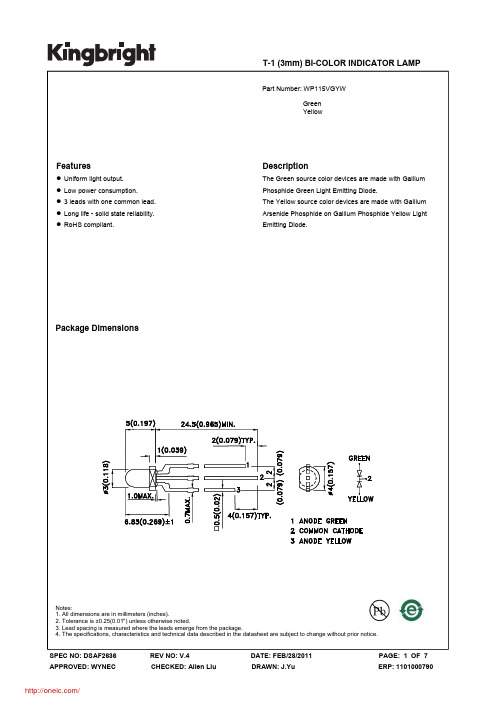
-40°C To +85°C 260°C For 3 Seconds 260°C For 5 Seconds
SPEC NO: DSAF2636 APPROVED: WYNEC
REV NO: V.4 CHECKED: Allen Liu
DATE: FEB/28/E: 2 OF 7 ERP: 1101000790
SPEC NO: DSAF2636 APPROVED: WYNEC
REV NO: V.4 CHECKED: Allen Liu
DATE: FEB/28/2011 DRAWN: J.Yu
PAGE: 7 OF 7 ERP: 1101000790
/
分销商库存信息:
KINGBRIGHT WP115VGYW
Part No. Dice Lens Type Iv (mcd) [2] @ 20mA Min. Green (GaP) WP115VGYW Yellow (GaAsP/GaP)
Notes: 1. θ1/2 is the angle from optical centerline where the luminous intensity is 1/2 of the optical peak value. 2. Luminous intensity/ luminous Flux: +/-15%.
Description
The Green source color devices are made with Gallium Phosphide Green Light Emitting Diode. The Yellow source color devices are made with Gallium Arsenide Phosphide on Gallium Phosphide Yellow Light Emitting Diode.
整流桥KBL06 KBL封装系列规格书推荐

PULSE WIDTH=300 µs
1%DUTY CYCLE
0.01
0.6
0.8
1.0
1.2
1.4 1.5
INSTANTANEOUS FORWARD VOLTAGE, VOLTS
INSTANTANEOUS REVERSE CURRENT, MICROAMPERES
FIG. 4-TYPICAL REVERSE CHARACTERISTICS
KBL 10
1000 700 1000
UNITS
VOLTS VOLTS VOLTS
Amps
Amps
A2s
Volts
µA mA pF C/W
C C
1 of 2
AVERAGE FORWARD RECTIFIED CURRENT, AMPERES
INSTANTANEOUS FORWARD CURRENT,AMPERES
Maximum DC blocking voltage
VDC
50 100 200 400 600 800
Maximum average forward TC=50 C(Note 2)
output rectified current at TA=50 C(Note 3)
I(AV)
4.0 3.0
Peak forward surge current
8.3ms single half sine-wave superimposed on
IFSM
200
rated load (JEDEC Method)
Rating for Fusing(t<8.3ms)
I2t
166
Maximum instantaneous forward voltage drop
vishay 1n5391 通用塑料整流器 数据表说明书

General Purpose Plastic RectifierFEATURES•Low forward voltage drop •Low leakage current•High forward surge capability•Solder dip 275 °C max. 10 s, per JESD 22-B106•Material categorization: for definitions of compliance please see /doc?99912TYPICAL APPLICATIONSFor use in general purpose rectification of power supplies, inverters, converters, and freewheeling diodes application.MECHANICAL DATACase: DO-41 (DO-204AL), molded epoxy bodyMolding compound meets UL 94 V-0 flammability rating Base P/N-E3 - RoHS-compliant, commercial grade Terminals: matte tin plated leads, solderable per J-STD-002 and JESD 22-B102E3 suffix meets JESD 201 class 1A whisker test Polarity: color band denotes cathode endPRIMARY CHARACTERISTICSI F(AV) 1.5 AV RRM 50 V, 100 V, 200 V, 300 V, 400 V, 500 V, 600 V, 800 V, 1000 VI FSM 50 A V F 1.4 V I R 5.0 μA T J max.150 °C Package DO-41 (DO-204AL)Circuit configurationSingleDO-41 (DO-204AL)MAXIMUM RATINGS (T A = 25 °C unless otherwise noted)PARAMETERSYMBOL 1N53911N53921N53931N53941N53951N53961N53971N53981N5399UNIT Maximum repetitive peak reverse voltage V RRM 501002003004005006008001000V Maximum RMS voltage V RMS 3570140210280350420560700V Maximum DC blocking voltage V DC 501002003004005006008001000V Maximum average forwardrectified current 0.500" (12.7 mm) lead length at T L = 70 °C I F(AV)1.5APeak forward surge current 8.3 ms single half sine-wave superimposed on rated load I FSM50AMaximum full load reversecurrent, full cycle average 0.375" (9.5 mm) lead length at T L = 70 °C I R(AV)300μA Operation junction and storage temperature rangeT J , T STG-50 to +150°CNote(1)Thermal resistance from junction to ambient at 0.375" (9.5 mm) lead length, PCB mountedRATINGS AND CHARACTERISTICS CURVES (T A = 25 °C unless otherwise noted)Fig. 1 - Forward Current Derating Curve Fig. 2 - Maximum Non-repetitive Peak Forward Surge CurrentELECTRICAL CHARACTERISTICS (T A = 25 °C unless otherwise noted)PARAMETER TEST CONDITIONS SYMBOL 1N53911N53921N53931N53941N53951N53961N53971N53981N5399UNIT Maximum instantaneous forward voltage 1.5 AT A = 70 °C V F1.4 V Maximum DC reverse current at rated DC blocking voltage T A = 25 °CI R5.0μAT A = 150 °C300Typical reverse recovery time I F = 0.5 A, I R = 1.0 A, I rr = 0.25 A t rr 2.0μs Typical junction capacitance4.0 V, 1 MHzC J15pFTHERMAL CHARACTERISTICS (T A = 25 °C unless otherwise noted)PARAMETERSYMBOL 1N53911N53921N53931N53941N53951N53961N53971N53981N5399UNIT Typical thermal resistanceR θJA (1)55°C/WR θJL (1)25ORDERING INFORMATION (Example)PREFERRED P/N UNIT WEIGHT (g)PREFERRED PACKAGE CODEBASE QUANTITYDELIVERY MODE1N5391-E3/540.33654550013" diameter paper tape and reel1N5391-E3/730.336733000Ammo pack packaging01.01.52.02550751001251501750.5Lead Temperature (°C)A v e r a g e F o r w a r d R e c t i fi e d C u r r e n t (A )01020305040110010Number of Cycle s at 60 HzP e a k F o r w a r d S u r g e C u r r e n t (A )Fig. 3 - Typical Instantaneous Forward Characteristics Fig. 4 - Typical Reverse Characteristics Fig. 5 - Typical Junction CapacitanceFig. 6 - Transient Thermal ImpedancePACKAGE OUTLINE DIMENSIONS in inches (millimeters)0.60.8 1.0 1.2 1.4 1.6 1.80.010.1101100I n s t a n t a n e o u s F o r w a r d C u r r e n t (A )In s tantaneou sForward Voltage (V)604020100800.010.11010010001Percent of Rated Peak Rever s e Voltage (%)I n s t a n t a n e o u s R e v e r s e L e a k a g e C u r r e n t (μA )0.1101100100101Rever s e Voltage (V)J u n c t i o n C a p a c i t a n c e (p F)1001010.1t - Pul s e Duration (s )0.010.1110100T r a n s i e n t T h e r m a l I m p e d a n c e (°C /W )DO-41 (DO-204AL)Legal Disclaimer Notice VishayDisclaimerALL PRODUCT, PRODUCT SPECIFICATIONS AND DATA ARE SUBJECT TO CHANGE WITHOUT NOTICE TO IMPROV E RELIABILITY, FUNCTION OR DESIGN OR OTHERWISE.V ishay Intertechnology, Inc., its affiliates, agents, and employees, and all persons acting on its or their behalf (collectively,“Vishay”), disclaim any and all liability for any errors, inaccuracies or incompleteness contained in any datasheet or in any other disclosure relating to any product.Vishay makes no warranty, representation or guarantee regarding the suitability of the products for any particular purpose or the continuing production of any product. To the maximum extent permitted by applicable law, Vishay disclaims (i) any and all liability arising out of the application or use of any product, (ii) any and all liability, including without limitation special, consequential or incidental damages, and (iii) any and all implied warranties, including warranties of fitness for particular purpose, non-infringement and merchantability.Statements regarding the suitability of products for certain types of applications are based on Vishay's knowledge of typical requirements that are often placed on Vishay products in generic applications. Such statements are not binding statements about the suitability of products for a particular application. It is the customer's responsibility to validate that a particular product with the properties described in the product specification is suitable for use in a particular application. Parameters provided in datasheets and / or specifications may vary in different applications and performance may vary over time. All operating parameters, including typical parameters, must be validated for each customer application by the customer's technical experts. Product specifications do not expand or otherwise modify Vishay's terms and conditions of purchase, including but not limited to the warranty expressed therein.Hyperlinks included in this datasheet may direct users to third-party websites. These links are provided as a convenience and for informational purposes only. Inclusion of these hyperlinks does not constitute an endorsement or an approval by Vishay of any of the products, services or opinions of the corporation, organization or individual associated with the third-party website. Vishay disclaims any and all liability and bears no responsibility for the accuracy, legality or content of the third-party website or for that of subsequent links.Except as expressly indicated in writing, Vishay products are not designed for use in medical, life-saving, or life-sustaining applications or for any other application in which the failure of the Vishay product could result in personal injury or death. Customers using or selling Vishay products not expressly indicated for use in such applications do so at their own risk. Please contact authorized Vishay personnel to obtain written terms and conditions regarding products designed for such applications. No license, express or implied, by estoppel or otherwise, to any intellectual property rights is granted by this document or by any conduct of Vishay. Product names and markings noted herein may be trademarks of their respective owners.© 2022 VISHAY INTERTECHNOLOGY, INC. ALL RIGHTS RESERVED。
伤害安誉A705UV点型紫外火焰探测器规格书
A705UV点型紫外火焰探测器规格书上海安誉智能科技有限公司地址:上海市张江高科祖冲之路887弄84号502室电话:021-********传真:021-********邮编:2012031概述本规格书描述了上海安誉智能科技有限公司(以下简称安誉)A705/UV点型紫外火焰探测器的主要技术规格,包括(但不限于)产品功能、技术参数、软件、硬件和光学系统的组成、安装调试、使用和维护方法等。
本规格书根据A705/UV设计文件编制,随着技术进步和产品应用实践,安誉将在国家标准和3C 管理相关规则限定的范围内对产品进行持续改进,使产品能够持续的满足用户的需求。
一旦实施产品改进,安誉有权修订和更新本规格书。
请关注本规格书最新版本。
2产品功能和组成A705/UV可应用于需要对火焰实施监控的场所,快速发现可能引起火灾的燃烧火焰,及时发出火灾警报。
A705/UV使用冷阴极紫外光电管将火焰燃烧参数转换为电脉冲信号,之后将信号输入工业计算芯片进行运算和处理,配合UVdetecter@anysafe专用智能控制软件,可以及时发出火灾警报。
A705/UV采用铝压铸隔爆壳体,具有良好的防爆和防护特性,耐腐蚀、抗老化,可以长期工作于室内、室外以及各种特殊的工业场所。
3技术参数3.1基本参数项目规格名称点型紫外火焰探测器型号A705/UV执行标准●GB12791-2006《点型紫外火焰探测器》●GB3836.1-2000《爆炸性气体环境用电气设备》第1部分:通用技术要求●GB3836.2-2000《爆炸性气体环境用电气设备》第2部分:隔爆型“D”传感器●HAMAMATSU R2868型冷阴极光电管光学窗口石英玻璃(SIO2)壳体●材料:铝合金●成型工艺:压铸●涂覆工艺:表面静电粉末喷涂,内部金属钝化处理。
重量≤1kg防爆和防护●防爆:EXdⅡCT6●防护:IP663.2工作参数项目规格或状态供电电源最小标准最大18VDC(可定制12VDC)24VDC30VDC工作电流监视状态≤20mA,报警状态≤35mA 预热时间通电后60s火灾报警当被监视区域发现火焰时,探测器进入火警状态;火警输出继电器动作,红色火警指示灯点亮;故障报警当发现传感器、电源等异常时,探测器进入故障报警状态;故障输出继电器动作,黄色故障指示灯点亮;当火警和故障同时发生时,火警优先;报警阈值1-5级可调(通过磁棒设定)监视状态每次绿灯闪烁次数表示报警阈值报警延迟0-30S可调(出厂时设置为0S)漂移补偿智能软件补偿模式可有效补偿因温度、环境变化和元器件长期工作产生的漂移干扰源抑制可有效抑制非火焰干扰源的影响,如阳光(直射和反射)、常用人工光源、电焊等指示灯●监视状态:绿灯闪亮●火警状态:红灯常亮●故障状态:黄灯常亮输出●火警继电器,报警时动作,输出触点3A@30VDC3A@250VAC ●故障继电器,故障时动作,输出触点3A@30VDC3A@250VAC ●串行通讯接口3.3探测性能和保护范围3.4环境参数项目规格工作温度-10℃—+55℃或-40℃—+70℃工作湿度≤95%HR,无结露储存温度-40℃—+85℃3.5设置和记录项目内容设置使用PC和专用软件,通过串行通讯口可设置探测器的报警参数:●报警模式●报警阈值●报警延迟时间需专业人士操作和密码授权简易设置利用手边的磁铁,控制内置干簧管调整报警灵敏度记录查询使用PC和专用软件,通过串行通讯口可查询探测器的内部记录●出厂设置:报警阈值、延迟时间。
MBR30H30CTG 开关电源整流器 30 V 30 A 用户手册说明书
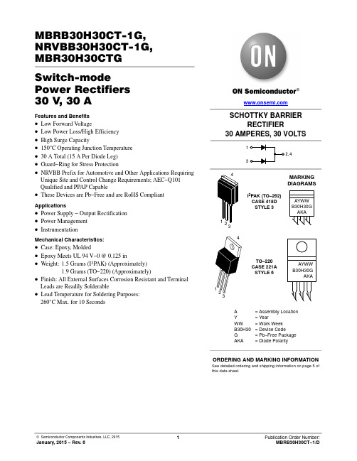
MBRB30H30CT-1G, NRVBB30H30CT-1G, MBR30H30CTG Switch-mode Power Rectifiers30 V, 30 AFeatures and Benefits•Low Forward V oltage•Low Power Loss/High Efficiency•High Surge Capacity•150°C Operating Junction Temperature•30 A Total (15 A Per Diode Leg)•Guard−Ring for Stress Protection•NRVBB Prefix for Automotive and Other Applications Requiring Unique Site and Control Change Requirements; AEC−Q101 Qualified and PPAP Capable•These Devices are Pb−Free and are RoHS CompliantApplications•Power Supply − Output Rectification•Power Management•InstrumentationMechanical Characteristics:•Case: Epoxy, Molded•EpoxyMeetsUL94V−*********•Weight:1.5 Grams (I2PAK) (Approximately)1.9 Grams (TO−220) (Approximately)•Finish: All External Surfaces Corrosion Resistant and Terminal Leads are Readily Solderable•Lead Temperature for Soldering Purposes:260°C Max. for 10 SecondsSCHOTTKY BARRIERRECTIFIER30 AMPERES, 30 VOLTS13MARKINGDIAGRAMSI2PAK (TO−262)CASE 418DSTYLE 3AYWWB30H30GAKA3TO−220CASE 221ASTYLE 6A= Assembly LocationY= YearWW= Work WeekB30H30= Device CodeG= Pb−Free PackageAKA= Diode PolaritySee detailed ordering and shipping information on page 5 of this data sheet.ORDERING AND MARKING INFORMATIONMAXIMUM RATINGS (Per Diode Leg)Rating Symbol Value UnitPeak Repetitive Reverse Voltage Working Peak Reverse Voltage DC Blocking Voltage V RRMV RWMV R30VAverage Rectified Forward Current (Rated V R) T C = 138°C I F(AV)15APeak Repetitive Forward Current (Rated V R, Square Wave, 20 kHz)I FRM30ANonrepetitive Peak Surge Current(Surge applied at rated load conditions halfwave, single phase, 60 Hz)I FSM260AOperating Junction Temperature (Note 1)T J−55 to +150°C Storage Temperature T stg*55 to +150°C Voltage Rate of Change (Rated V R)dv/dt10,000V/m s Controlled Avalanche Energy (see test conditions in Figures 9 and 10)W AVAL250mJ ESD Ratings:Machine Model = C Human Body Model = 3B> 400> 8000VStresses exceeding those listed in the Maximum Ratings table may damage the device. If any of these limits are exceeded, device functionality should not be assumed, damage may occur and reliability may be affected.1.The heat generated must be less than the thermal conductivity from Junction−to−Ambient: dP D/dT J < 1/R q JA.THERMAL CHARACTERISTICSRating Symbol Value Unit Maximum Thermal ResistanceJunction−to−Case Junction−to−Ambient R q JCR q JA2.070°C/WELECTRICAL CHARACTERISTICS (Per Diode Leg)Rating Symbol Value UnitMaximum Instantaneous Forward Voltage (Note 2) (I F = 15 A, T C = 25°C)(I F = 15 A, T C = 125°C)(I F = 30 A, T C = 25°C)(I F = 30 A, T C = 125°C)v F0.480.400.550.53VMaximum Instantaneous Reverse Current (Note 2) (Rated DC Voltage, T C = 25°C)(Rated DC Voltage, T C = 125°C)i R0.8130mAProduct parametric performance is indicated in the Electrical Characteristics for the listed test conditions, unless otherwise noted. Product performance may not be indicated by the Electrical Characteristics if operated under different conditions.2.Pulse Test: Pulse Width = 300 m s, Duty Cycle ≤ 2.0%.I F , I N S T A N T A N E O U S F O R W A R D C U R R E N T (A M P S )Figure 1. Typical Forward Voltage Figure 2. Maximum Forward VoltageV F , INSTANTANEOUS FORWARD VOLTAGE (VOLTS)10010.10.40.21.00.80.6I R , R E V E R S E C U R R E N T (A M P S )Figure 3. Typical Reverse Current Figure 4. Maximum Reverse Current50V R , REVERSE VOLTAGE (VOLTS)10I F , A V E R A G E F O R W A R D C U R R E N T (A M P S )Figure 5. Current DeratingT C , CASE TEMPERATURE (°C)1201101050140150130160P F O , A V E R A G E P O W E R D I S S I P A T I O N (W A T T S )15I O , AVERAGE FORWARD CURRENT (AMPS)1620510Figure 6. Forward Power Dissipation100.1101520301004681214301525202025250.30.50.70.9I F , I N S T A N T A N E O U S F O R W A R D C U R R E N T (A M P S )V F , INSTANTANEOUS FORWARD VOLTAGE (VOLTS)10010.10.40.21.00.80.60.1100.30.50.70.9I R )50V R , REVERSE VOLTAGE (VOLTS)1015203025C , C A P A C I T A N C E (p F )0V R , REVERSE VOLTAGE (VOLTS)1500025Figure 7. Typical Capacitance2010153000302000250010005005R (t ), T R A N S I E N T T H E R M A L R E S I S T A N C EFigure 8. Thermal Response Junction−to−Caset 1, TIME (sec)BV DUTI L I DV DDt0t1t2t Figure 9. Test Circuit Figure 10. Current−Voltage WaveformsThe unclamped inductive switching circuit shown in Figure 9 was used to demonstrate the controlled avalanche capability of this device. A mercury switch was used instead of an electronic switch to simulate a noisy environment when the switch was being opened.When S1 is closed at t0 the current in the inductor I L ramps up linearly; and energy is stored in the coil. At t1 the switch is opened and the voltage across the diode under test begins to rise rapidly, due to di/dt effects, when this induced voltage reaches the breakdown voltage of the diode, it is clamped at BV DUT and the diode begins to conduct the full load current which now starts to decay linearly through the diode, and goes to zero at t2.By solving the loop equation at the point in time when S1 is opened; and calculating the energy that is transferred to the diode it can be shown that the total energy transferred is equal to the energy stored in the inductor plus a finite amount of energy from the V DD power supply while the diode is in breakdown (from t1 to t2) minus any losses due to finite component resistances. Assuming the component resistive elements are small Equation (1) approximates the total energy transferred to the diode. It can be seen from this equation that if the V DD voltage is low compared to the breakdown voltage of the device, the amount of energy contributed by the supply during breakdown is small and the total energy can be assumed to be nearly equal to the energy stored in the coil during the time when S1 was closed, Equation (2).W AVAL[12LI2LPKǒBV DUTBV DUT–V DDǓW AVAL[12LI2LPKEQUATION (1):EQUATION (2):ORDERING INFORMATIONDevice Package Shipping MBRB30H30CT−1G TO−262(Pb−Free)50 Units / RailNRVBB30H30CT−1G TO−262(Pb−Free)50 Units / RailMBR30H30CTG TO−220(Pb−Free)50 Units / RailTO −220CASE 221A ISSUE AKDATE 13 JAN 2022STYLE 1:PIN 1.BASE2.COLLECTOR3.EMITTER4.COLLECTORSTYLE 2:PIN 1.BASE 2.EMITTER 3.COLLECTOR 4.EMITTERSTYLE 3:PIN 1.CATHODE 2.ANODE 3.GATE 4.ANODESTYLE 4:PIN 1.MAIN TERMINAL 12.MAIN TERMINAL 23.GATE4.MAIN TERMINAL 2STYLE 7:PIN 1.CATHODE 2.ANODE 3.CATHODE 4.ANODE STYLE 10:PIN 1.GATE 2.SOURCE 3.DRAIN 4.SOURCE STYLE 5:PIN 1.GATE 2.DRAIN 3.SOURCE 4.DRAIN STYLE 8:PIN 1.CATHODE 2.ANODE3.EXTERNAL TRIP/DELAY4.ANODESTYLE 6:PIN 1.ANODE 2.CATHODE 3.ANODE 4.CATHODE STYLE 9:PIN 1.GATE2.COLLECTOR3.EMITTER4.COLLECTOR STYLE 11:PIN 1.DRAIN 2.SOURCE 3.GATE 4.SOURCE STYLE 12:PIN 1.MAIN TERMINAL 12.MAIN TERMINAL 23.GATE4.NOT CONNECTEDI 2PAK (TO −262)CASE 418D −01ISSUE DDATE 16 OCT 2007NOTES:1.DIMENSIONING AND TOLERANCING PER ANSI Y14.5M, 1982.2.CONTROLLING DIMENSION: INCH.STYLE 1:PIN 1.BASE2.COLLECTOR3.EMITTER4.COLLECTORSTYLE 2:PIN 1.GATE 2.DRAIN 3.SOURCE 4.DRAINSTYLE 3:PIN 1.ANODE 2.CATHODE 3.ANODE 4.CATHODESTYLE 4:PIN 1.GATE2.COLLECTOR3.EMITTER4.COLLECTORD DIM MIN MAX MIN MAX MILLIMETERSINCHES A 0.3350.3808.519.65B 0.3800.4069.6510.31C 0.1600.185 4.06 4.70D 0.0260.0350.660.89E 0.0450.055 1.14 1.40G 0.100 BSC 2.54 BSC H 0.0940.110 2.39 2.79J 0.0130.0250.330.64S 0.390 REF 9.90 REF V 0.0450.070 1.14 1.78W0.5220.55113.2514.00MBM 0.13 (0.005)T F 0.122 REF 3.10 REF K 0.5000.56212.7014.27ON Semiconductor and are trademarks of Semiconductor Components Industries, LLC dba ON Semiconductor or its subsidiaries in the United States and/or other countries.ON Semiconductor reserves the right to make changes without further notice to any products herein. ON Semiconductor makes no warranty, representation or guarantee regarding the suitability of its products for any particular purpose, nor does ON Semiconductor assume any liability arising out of the application or use of any product or circuit, and specifically disclaims any and all liability, including without limitation special, consequential or incidental damages. ON Semiconductor does not convey any license under its patent rights nor thePUBLICATION ORDERING INFORMATIONTECHNICAL SUPPORTNorth American Technical Support:Voice Mail: 1 800−282−9855 Toll Free USA/Canada Phone: 011 421 33 790 2910LITERATURE FULFILLMENT :Email Requests to:*******************onsemi Website: Europe, Middle East and Africa Technical Support:Phone: 00421 33 790 2910For additional information, please contact your local Sales Representative。
高功率UV-A LED数据手册说明书
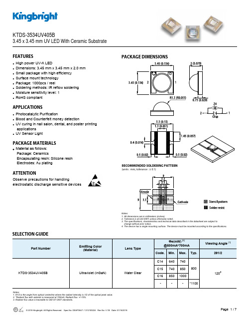
FEATURESzHigh power UV-A LEDz Dimensions: 3.45 mm x 3.45 mm x 2.0 mm z Small package with high efficiency z Surface mount technology z Package: 1000pcs / reelz Soldering methods: IR reflow soldering z Moisture sensitivity level: 1 z RoHS compliantAPPLICATIONSzPhotocatalytic Purificationz Blood and Counterfeit money detectionz UV curing in nail salon, dental, and poster printing applications z UV Sensor LightPACKAGE MATERIALSzMaterial as follows: Package: CeramicsEncapsulating resin: Silicone resin Electrodes: Au platingATTENTIONObserve precautions for handlingelectrostatic discharge sensitive devicesPACKAGE DIMENSIONSSELECTION GUIDEKTDS-3534UV405B3.45 x 3.45 mm UV LED With Ceramic SubstrateRECOMMENDED SOLDERING PATTERN(units : mm; tolerance : ± 0.1)Notes:1. All dimensions are in millimeters (inches).2. Tolerance is ±0.2(0.008") unless otherwise noted.3. The specifications, characteristics and technical data described in the datasheet are subject to change without prior notice.4. The device has a single mounting surface. The device must be mounted according to the specifications.Notes:1. θ1/2 is the angle from optical centerline where the radiant intensity is 1/2 of the optical peak value.2. *Radiant flux with asterisk is measured at 700mA; Radiant flux: +/-15%.3. Radiant flux value is traceable to CIE127-2007 standards.Part NumberEmitting Color (Material)Lens TypeΦe(mW) [2] @500mA*700mA Viewing Angle [1]Code. Min. Max. Typ. 2θ1/2KTDS-3534UV405BUltraviolet (InGaN)Water ClearC14 640 740 120°C15740850C16 850 1000 ---*1100800ABSOLUTE MAXIMUM RATINGS at T A =25°CELECTRICAL / OPTICAL CHARACTERISTICS at T A =25°CNotes:1. Forward voltage: ±0.1V.2. Wavelength value is traceable to CIE127-2007 standards.3. Excess driving current and / or operating temperature higher than recommended conditions may result in severe light degradation or premature failure.ParameterSymbol Value UnitWavelength at Peak Emission I F = 500mA [Min.] λpeak 400Wavelength at Peak Emission I F = 500mA [Typ.] 405 Wavelength at Peak Emission I F = 500mA [Max.] 410Spectral Bandwidth at 50% Φ REL MAX I F = 500mA [Typ.] Δλ15 nmForward Voltage I F = 500mA [Typ.]V F [1]3.4VForward Voltage I F = 500mA [Max.] 3.9 Allowable Reverse Current [Max.] I R 85 mA Temperature Coefficient of V FI F = 500mA, -10°C ≤ T ≤ 100°CTC V-3.0mV/°CnmParameterSymbolValueUnitPower Dissipation P D 2.8 W Reverse Voltage V R 5 V Junction Temperature T j [1] 115 °C Operating Temperature T op -40 to +100 °C Storage Temperature T stg -40 to +115°C DC Forward Current I F [1] 700 mA Peak Forward CurrentI FM [2] 1000 mA Thermal Resistance (Junction / Ambient) R th JA [1] 10 °C/W Thermal Resistance (Junction / Solder point)R th JS [1]5°C/WNotes:1. Results from mounting on metal core PCB, mounted on pc board-metal core PCB is recommend for lowest thermal resistance.2. 1/10 Duty Cycle, 0.1ms Pulse Width.3. Relative humidity levels maintained between 40% and 60% in production area are recommended to avoid the build-up of static electricity – Ref JEDEC/JESD625-A and JEDEC/J-STD-033.TECHNICAL DATAULTRAVIOLETTAPE SPECIFICATIONS (units : mm) REEL DIMENSION (units : mm)HANDLING PRECAUTIONSCompare to epoxy encapsulant that is hard and brittle, silicone is softer and flexible. Although its characteristic significantly reduces thermal stress, it is more susceptible to damage by external mechanical force. As a result, special handling precautions need to be observed during assembly using silicone encapsulated LED products. Failure to comply might lead to damage and premature failure of the LED. 3. Do not stack together assembled PCBs containing exposed LEDs. Impact may scratch the silicone lens or damage the internal circuitry.2. Do not directly touch or handle the silicone lens surface. It may damage the internal circuitry.1. Handle the component along the side surfaces by using forceps or appropriate tools.Designing the Position of LED on a Board1. No twist / warp / bent / or other stress shall be applied to the board after mounting LED with solder to avoid a crack of LED package. Refer to the following recommended position and direction of LED.3. Do not split board by hand. Split with exclusive special tool.4. If an aluminum circuit board is used, a large stress by thermal shock might cause a solder crack. For this reason, it is recommended an appropriate verification should be taken before use.Appropriate LED mounting is to place perpendicularly against the stress affected side . 2. Depending on the position and direction of LED,the mechanical stress on the LED package can be changed.Refer to the following figure.JEDEC Moisture SensitivityLevelFloor LifeSoak RequirementsStandardAccelerated Equivalent Time ConditionsTime (hours) Conditions Time (hours)Conditions1Unlimited≤ 30 °C / 85% RH168 + 5 / - 085 °C / 85% RH--Kingbright recommends keeping the LEDs in the sealed moisture-barrier packaging until immediately prior to use. Any unused LEDs should be returned to the moisture-barrier bag and closed immediately after use.4-1. There should be enough space inside the nozzle to avoid contact with the dome lens during pick up. 4-2. The inner diameter of the SMD pickup nozzle should not exceed the size of the LED to prevent air leaks. 4-3. A pliable material is suggested for the nozzle tip to avoid scratching or damaging the LED surface during pickup. 4-4. The dimensions of the component must be accurately programmed in the pick-and-place machine to insure precise pickup and avoid damage during production.5. As silicone encapsulation is permeable to gases, some corrosive substances such as H 2S might corrode silver plating of lead-frame. Special care should be taken if an LED with silicone encapsulation is to be used near such substances.ESD Protection During ProductionElectric static discharge can result when static-sensitive products come in contact with the operator or other conductors.The following procedures may decrease the possibility of ESD damage:1. Minimize friction between the product and surroundings to avoid static buildup.2. All production machinery and test instruments must be electrically grounded.3. Operators must wear anti-static bracelets.4. Wear anti-static suit when entering work areas with conductive machinery.5. Set up ESD protection areas using grounded metal plating for component handling.6. All workstations that handle IC and ESD-sensitive components must maintain an electrostatic potential of 150V or less.7. Maintain a humidity level of 50% or higher in production areas.8. Use anti-static packaging for transport and storage.9. All anti-static equipment and procedures should be periodically inspected and evaluated for proper functionality.Heat Generation1. Thermal design of the end product is of paramount importance. Please consider the heat generation of the LED when making the system design.The coefficient of temperature increase per input electric power is affected by the thermal resistance of the circuit board and density of LED placement on the board, as well as other components. It is necessary to avoid intense heat generation and operate within the maximum ratings given in thisspecification.2. Please determine the operating current with consideration of the ambient temperature local to the LED and refer to the plot of Permissible Forward Current vs. Ambient temperature on characteristics in this specification.Please also take measures to remove heat from the area near the LED to improve the operational characteristics on the LED.3. The equation ①indicates correlation between T j and T a, and the equation ② indicates correlation between T j and T sT j = T a + R th JA *W ……… ①T j = T s + R th JS *W ……… ②T j = dice junction temperature: °CT a = ambient temperature: °CT s = solder point temperature: °CR th JA = heat resistance from dice junction temperature to ambient temperature: °C / WR th JS = heat resistance from dice junction temperature to Ts measuring point: °C / WW = inputting power (I F x V F): WREFLOW SOLDERING PROFILE for LEAD-FREE SMD PROCESSNotes:1. Don't cause stress to the LEDs while it is exposed to high temperature.2. The maximum number of reflow soldering passes is 2 times.3. Reflow soldering is recommended. Other soldering methods are not recommended as they mightcause damage to the product.Criteria For Judging DamageItemSymbol Test Conditions Criteria for JudgementMin. Max. Forward Voltage V F I F = 500mA -Initial Level x 1.1Radiant FluxΦeI F = 500mAInitial Level x 0.7-Note: The test is performed after the board is cooled down to the room temperature.RELIABILITY TEST ITEMS AND CONDITIONSThe reliability of products shall be satisfied with items listed below Lot Tolerance Percent Defective (LTPD) : 10%No. Test ItemStandardsTest ConditionTest Times / CyclesNumber of Damaged 1 Continuous operating test - T a = 25°C +10/-5°C, RH = 55+/-20%RHI F = maximum rated current*1,000 h0 / 22 2 High Temp. operating test - T a = 100°C(+/-10°C)I F = maximum rated current*1,000 h0 / 22 3 Low Temp. operating test -T a = -40°C+3/-5°CI F = maximum rated current*1,000 h0 / 22 4 High temp. storage test JEITA ED-4701/200 201 T a = 100°C(+/-10°C)T a = maximum rated storage temperature1,000 h0 / 22 5 Low temp. storage test JEITA ED-4701/200 202 T a = -40°C+3/-5°C1,000 h 0 / 22 6 High temp. & humidity storage testJEITA ED-4701/100 103T a = 60°C+5/-3°C, RH = 90+5/-10%RH 1,000 h 0 / 22 7 High temp. & humidity operating test-T a = 60°C+5/-3°C, RH = 90%+5/-10%RHI F = maximum rated current*1,000 h 0 / 22 8 Resistance to Soldering Heat(Reflow Soldering)JEITA ED-4701/300 301Tsld = 260°C, 10sec 2 times 0 / 22 9Solderability(Reflow Soldering)JEITA ED-4701/303 303ATsld = 245°C+/-5°C, 5+/-1sec 1 time over 95%0 / 2210 Temperature Cycle operating test--40°C(30min) ~ 25°C(5min) ~ 100°C(30min) ~ 25°C(5min) I F = derated current at 100°C 10 cycles 0 / 2211 Temperature Cycle JEITA ED-4701/100 105-40°C(30min) ~ 25°C(5min) ~ 100°C(30min) ~ 25°C(5min) 100 cycles 0 / 22 12 Thermal shock testMIL-STD-202G T a = -40°C(15min) ~ 100°C(15min) 500 cycles 0 / 22 13Electric Static Discharge (ESD)JEITA ED-4701/300 304C = 100pF, R = 1.5K Ω V = 8000V3 times Negative / Positive0 / 2214 Vibration test JEITA ED-4701/400 403100 ~ 2000 ~ 100HZ Sweep 4min.200m/s²3directions, 4cycles48 min. 0 / 22Note: Refer to forward current vs. derating curve diagram.PACKING & LABEL SPECIFICATIONSPackaging1.The LEDs are packed in cardboard boxes after taping.2.The label on the minimum packing unit shows: Part Number, Lot Number, Ranking, Quantity.3.In order to protect the LEDs from mechanical shock, we pack them in cardboard boxes for transportation.4.The LEDs may be damaged if the boxes are dropped or receive a strong impact against them, so precautionsmust be taken to prevent any damage.5.The boxes are not water resistant and therefore must be kept away from water and moisture.6.When the LEDs are transported, we recommend that you use the same packing methods as Kingbright’s.PRECAUTIONARY NOTES1. The information included in this document reflects representative usage scenarios and is intended for technical reference only.2. The part number, type, and specifications mentioned in this document are subject to future change and improvement without notice. Before production usage customer should refer tothe latest datasheet for the updated specifications.3. When using the products referenced in this document, please make sure the product is being operated within the environmental and electrical limits specified in the datasheet. Ifcustomer usage exceeds the specified limits, Kingbright will not be responsible for any subsequent issues.4. The information in this document applies to typical usage in consumer electronics applications. If customer's application has special reliability requirements or have life-threateningliabilities, such as automotive or medical usage, please consult with Kingbright representative for further assistance.5. The contents and information of this document may not be reproduced or re-transmitted without permission by Kingbright.6. All design applications should refer to Kingbright application notes available at /application_notes。
整流器技术规格书

供电系统整流器技术规格书2009年6月目录1.总则 (2)1.1本文件适用围 (2)1.2供货围设备类型 (2)2.工程概况 (2)2.1工程说明 (2)2.2环境条件 (2)2.3系统运行方式 (2)2.4相关系统和设备参数 (3)3.设备数量 (4)4.主要元器件清单 (5)5.备品备件、测试工具 (5)6.整流器技术要求 (6)6.1采用标准 (6)6.2技术规格及要求 (7)6.3结构要求 (9)6.4设备的互换性 (10)6.5铭牌 (10)6.6试验容 (10)6.7接口 (11)7.设备其它要求 (12)7.1工艺要求和防锈 (12)7.2可靠性、可维护性、电磁辐射及兼容 (12)7.3柜体的颜色 (13)7.4标示 (13)1.总则1.1本文件适用围本文件适用于地铁15号线一期工程整流器设备供货,并作为供应商供货设备的技术依据。
1.2供货围设备类型整流器柜、备品备件和专用工具。
2.工程概况2.1工程说明地铁15号线位于东北部地区,主要分布在海淀、、顺义三个行政区。
线路起点位于西苑,沿颐和园路、清华西路下穿地铁4号线、穿过清华大学,沿清华东路向东,穿过八达岭高速公路,至奥林匹克中心区,沿大屯路继续向东至鼎成路转向南,穿过京承高速至望京西后,沿湖光中街进入望京核心区域,再向北至望京北扩地区,折向东沿香江北路敷设,逐渐由地下出地面,线路以高架形式沿京顺路向北,跨过机场南线、温榆河、枯柳树环岛、机场北线后转向东,沿顺于路敷设,在东六环路西侧转向地下,沿顺义区府前街敷设,向东过潮白河后到达河东地区。
全线设一座车辆段和一座停车场,在香江北路设马泉营车辆段,在河东设停车场。
一期工程从北沙滩至顺义河东,线路长度38.3km,车站17座,其中4座为高架车站,13座为地下车站,最大站间距4.58km,最小站间距0.9km,平均站间距为2.32km。
2010年开通为望京西站至后沙峪站区段。
本线控制中心设在小营线网指挥中心二期。
功率肖特基整流器技术规格书Power Schottky rectifier

Power Schottky rectifierDatasheet - production dataFeatures∙Very small conduction losses∙Negligible switching losses∙Low forward voltage drop∙Avalanche specification∙ECOPACK®2 compliant component for DPAK on demand DescriptionDual center tab Schottky rectifier suited for switched mode power supply and high frequency DC to DC converters.Packaged in DPAK, this device is intended for use in low voltage, high frequency inverters, free-wheeling and polarity protection applications.Table 1. Device summary Symbol Value I F(AV) 2 x 7.5 A V RRM60 V T j(max)150 °C V F (typ)0.52 VCharacteristics1 CharacteristicsWhen the diodes 1 and 2 are used simultaneously:∆ T j (diode 1) = P(diode1) x R th(j-c)(Per diode) + P(diode 2) x R th(c)To evaluate the conduction losses use the following equation:P = 0.32 x I F(AV) + 0.027 I F 2(RMS)Table 2. Absolute ratings (limiting values per diode at 25 °C unless otherwise stated)Symbol ParameterValue UnitV RRM Repetitive peak reverse voltage 60V I F(RMS)Forward rms current10A I F(AV)Average forward current, δ = 0.5, squarewave T c = 135 °C (1)Per diode 7.5A Per device 15I FSM Surge non repetitive forward current t p = 10 ms sinusoidal 75A P ARM Repetitive peak avalanche power t p = 10 µs, T j = 125 °C265WT stg Storage temperature range-65 to +175°C T jMaximum operating junction temperature (2)150°C1.Value based on R th(j-c) max (per diode)2.condition to avoid thermal runaway for a diode on its own heatsink dPtot dTj---------------1Rth j a –()-------------------------<Table 3. Thermal resistancesSymbol ParameterValue UnitR th(j-c)Junction to case Per diode 4°C/W Total2.4R th(c)Coupling0.7Table 4. Static electrical characteristics (per diode)Symbol ParameterTest ConditionsMin.Typ.Max.Unit I R (1)Reverse leakage currentT j = 25 °C V R = V RRM200µA T j = 125 °C 4560mAV F (1)Forward voltage dropT j = 25 °C I F = 7.5 A0.62VT j = 125 °C0.520.57T j = 25 °C I F = 12 A0.76T j = 125 °C 0.620.68T j = 25 °C I F = 15 A0.82T j = 125 °C0.660.721.Pulse test: t p = 380 µs, δ < 2%CharacteristicsPackage Information 2 PackageInformation∙Epoxy meets UL94,V0∙Cooling method: by conduction (C)2.1 In order to meet environmental requirements, ST offers these devices in different grades of ECOPACK® packages, depending on their level of environmental compliance. ECOPACK® specifications, grade definitions and product status are available at: ECOPACK® is an ST trademark.DPAK package informationNote:This package drawing may slightly differ from the physical package. However, all the specified dimensions are guaranteed.Package InformationTable 5. DPAK package mechanical dataRef.DimensionsMillimetersInches Min.Typ.Max.Min.Typ.Max.A 2.18 2.400.0850.094A10.90 1.100.0350.043A20.030.230.0010.009b 0.640.900.0250.035b4 4.95 5.460.1940.214c 0.460.610.0180.024c20.460.600.0180.023D 5.97 6.220.2350.244D1 4.95 5.600.1940.220E 6.35 6.730.2500.264E1 4.325.500.1700.216e 2.280.090e1 4.40 4.700.1730.185H 9.3510.400.3680.409L 1.00 1.780.0390.070L2 1.270.050L40.60 1.020.0230.040V2-8°+8°-8°8°。
