超低功耗蓝牙无线SOC芯片 富芮坤创业大赛PPT(4-3)
Silicon Labs Bluetooth Low Energy 5.3产品简介说明书
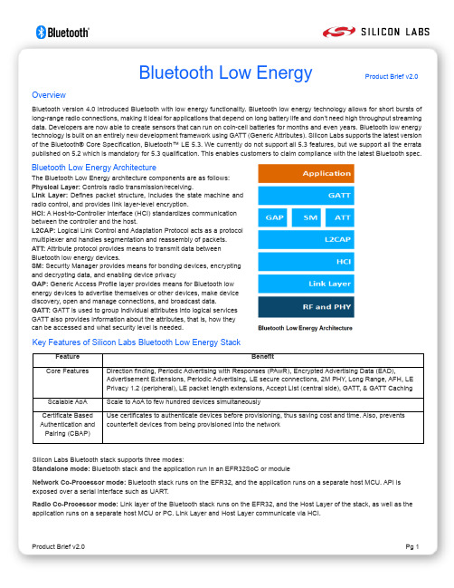
Bluetooth Low EnergyProduct Brief v2.0OverviewBluetooth version 4.0 introduced Bluetooth with low energy functionality. Bluetooth low energy technology allows for short bursts of long-range radio connections, making it ideal for applications that depend on long battery life and don’t need high throughput streaming data. Developers are now able to create sensors that can run on coin-cell batteries for months and even years. Bluetooth low energy technology is built on an entirely new development framework using GATT (Generic Attributes). Silicon Labs supports the latest version of the Bluetooth® Core Specification, Bluetooth™ LE 5.3. We currently do not support all 5.3 features, but we support all the errata published on 5.2 which is mandatory for 5.3 qualification. This enables customers to claim compliance with the latest Bluetooth spec.Bluetooth Low Energy ArchitectureThe Bluetooth Low Energy architecture components are as follows: Physical Layer: Controls radio transmission/receiving.Link Layer: Defines packet structure, includes the state machine and radio control, and provides link layer-level encryption.HCI: A Host-to-Controller interface (HCI) standardizes communication between the controller and the host.L2CAP: Logical Link Control and Adaptation Protocol acts as a protocol multiplexer and handles segmentation and reassembly of packets. ATT: Attribute protocol provides means to transmit data between Bluetooth low energy devices.SM: Security Manager provides means for bonding devices, encrypting and decrypting data, and enabling device privacyGAP: Generic Access Profile layer provides means for Bluetooth low energy devices to advertise themselves or other devices, make device discovery, open and manage connections, and broadcast data.GATT: GATT is used to group individual attributes into logical services GATT also provides information about the attributes, that is, how they can be accessed and what security level is needed.Key Features of Silicon Labs Bluetooth Low Energy StackFeature BenefitCore FeaturesDirection finding, Periodic Advertising with Responses (PAwR), Encrypted Advertising Data (EAD),Advertisement Extensions, Periodic Advertising, LE secure connections, 2M PHY , Long Range, AFH, LE Privacy 1.2 (peripheral), LE packet length extensions, Accept List (central side), GATT, & GATT Caching Scalable AoA Scale to AoA to few hundred devices simultaneouslyCertificate Based Authentication and Pairing (CBAP) Use certificates to authenticate devices before provisioning, thus saving cost and time. Also, prevents counterfeit devices from being provisioned into the networkSilicon Labs Bluetooth stack supports three modes:Standalone mode: Bluetooth stack and the application run in an EFR32SoC or moduleNetwork Co-Processor mode: Bluetooth stack runs on the EFR32, and the application runs on a separate host MCU. API is exposed over a serial interface such as UART.Radio Co-Processor mode: Link layer of the Bluetooth stack runs on the EFR32, and the Host Layer of the stack, as well as the application runs on a separate host MCU or PC. Link Layer and Host Layer communicate via HCI.Technical ResourcesBluetooth Low Energy xG24 Technical Library Data Sheets, App Notes, and moreBluetooth Low Energy xG21 Technical Library Data Sheets, App Notes, and moreBluetooth Low Energy xG22 Technical Library Data Sheets, App Notes, and moreBluetooth Low Energy API Documentation Bluetooth Low Energy API documentationSilicon Labs’ Bluetooth Low Energy HW supportHigh Performance device for Bluetooth LE and Bluetooth mesh applications thatrequire advance features and more Flash and RAMIndustry-leading, energyefficient device for Bluetooth LE applicationsOptimized for line-powered devices including LED bulbs, and gateways for Bluetooth LE and Bluetooth mesh• 1536kB Flash • 256kB RAM • TX power 19.5dBm • -105.7dBm @ 125kbps • -97.6dBm @ 1Mbit/s • -94.8dBm @ 2Mbit/s • RX current 4.4mA @ 1Mbps • TX current 5.0mA @ 0dBm • 1.3 µA Sleep current (16kB ) • Robust peripheral set • AI/ML hardware accelerator • Secure Vault High • QFN40 5x5 (26) •QFN48 6x6 (32)• 512kB Flash • 32kB RAM • TX power 6dBm • -106.7dBm @ 125kbps • -98.9dBm @ 1Mbit/s • -96.2dBm @ 2Mbit/s • RX current 3.6mA @ 1Mbps • TX current 4.1mA @ 0dBm • 1.26µA Sleep current (16kB ) • Lowest Power Bluetooth LE • Secure Vault Mid • QFN40 5x5 (26) • QFN32 4x4 (18) •TQFN32 4x4 (18)• 1024kB Flash • 96kB RAM • TX power 20dBm • -104.9dBm @ 125kbps • -97.5dBm @ 1Mbit/s • -94.4dBm @ 2Mbit/s • RX current 8.8mA @ 1Mbps • TX current 9.3mA @ 0dBm • +135 Junction Temperature • Secure Vault High • Line-Powered Bluetooth LE •QFN32 4x4 (20)Bluetooth LE Target Applications• ESL • Medical• Direction Finding • Smart Home • Smart Tags • Sensors • Switches• Building Automation • HVACBluetooth LE Software / ToolsSilicon Labs Bluetooth Low Energy SDK helps you build smooth, reliable, and secure wireless connectivity for your IoT applications. Software and Tools features • Supports Bluetooth™ LE 5.3 • Wi-Fi Coexistence • Simplicity Studio IDE • GATT Configurator • Network Analyzer• Direction Finding Tool suite • Bluetooth NCP Commander • Proprietary Radio Configurator • Energy Profiler• Tool Chain – GCC and IARLinks: Bluetooth Low Energy SDKLearning CenterReady for Bluetooth 5.4?Learn more about the latest specification Bluetooth Direction FindingBluetooth Location Services: AoA/AoD Why EFR?Silicon Labs EFR32 FeaturesSilicon Labs Secure Vault accreditations Product security certificationsBluetooth SoC and Module Selector Guide Bluetooth Low Energy Selector Guide Case Study: Rethinking Epilepsy Management EFR32 Portable Medical DeviceBluetooth BeaconsBluetooth Beacons and AdvertisingSilicon Labs’ Bluetooth LE Development KitsSilicon Labs’ Bluetooth development kits are divided into three categories based on your development need:• Rapid Prototyping • Proof of Concept• Advanced RF DevelopmentFor more information on the portfolio, check the link: https:///bluetooth-kitsBG22BG21BG24Disclaimer: Silicon Labs intends to provide customers with the latest, accurate, and in-depth documentation of all peripherals and modules available forsystem and software implementers using or intending to use the Silicon Labs products. Characterization data, available modules and peripherals, memory sizes and memory addresses refer to each specific device, and “Ty pical ” parameters provided can and do vary in different applications. Application examples described herein are for illustrative purposes only. Silicon Labs reserves the right to make changes without further notice to the product information, specifications, and descriptions herein, and does not give warranties as to the accuracy or completeness of the included information. Without prior notification, Silicon Labs may update product firmware during the manufacturing process for security or reliability reasons. Such changes will not alter the specifications or the performance of the product. Silicon Labs shall have no liability for the consequences of use of the information supplied in this document. This document does not imply or expressly grant any license to design or fabricate any integrated circuits. The products are not designed or authorized to be used within any FDA Class III devices, applications for which FDA premarket approval is required or Life Support Systems without the specific written consent of Silicon Labs. A “L ife Support System ” is any product or system intended to support or sustain life and/or health, which, if it fails, can be reasonably expected to result in significant personal injury or death. Silicon Labs products are not designed or authorized for military applications. Silicon Labs products shall under no circumstances be used in weapons of mass destruction including (but not limited to) nuclear, biological or chemical weapons, or missiles capable of delivering such weapons. Silicon Labs disclaims all express and implied warranties and shall not be responsible or liable for any injuries or damages related to use of a Silicon Labs product in such unauthorized applications. Note: This content may contain offensive terminology that is now obsolete. Silicon Labs is replacing these terms with inclusive language wherever possible. For more information, visit /about-us/inclusive-lexicon-projectTrademark InformationSilicon Laboratories Inc.®, Silicon Laboratories ®, Silicon Labs ®, SiLabs ® and the Silicon Labs logo ®, Bluegiga ®, Bluegiga Logo ®, EFM ®, EFM32®, EFR, Ember ®, Energy Micro, Energy Micro logo and combinations thereof, “the world ’s most energy friendly microcontroller s”, Redpine Signals ®, WiSeConnect , n-Link, ThreadArch ®, EZLink ®, EZRadio ®, EZRadioPRO ®, Gecko ®, Gecko OS, Gecko OS Studio, Precision32®, Simplicity Studio ®, Telegesis, the Telegesis Logo ®, USBXpress ® , Zentri, the Zentri logo and Zentri DMS, Z-Wave ®, and others are trademarks or registered trademarks of Silicon Labs. ARM, CORTEX, Cortex-M3 and THUMB are trademarks or registered trademarks of ARM Holdings. Keil is a registered trademark of ARM Limited. Wi-Fi is a registered trademark of the Wi-Fi Alliance. All other products or brand names mentioned herein are trademarks of their respective holders.Silicon Laboratories Inc. 400 West Cesar Chavez Austin, TX 78701IoT PortfolioQualitySupport & Community/products/quality/community。
创业培训GYB课件(实际用)

2023/10/25
41
企业创办者应具备的特征
物质条件 家庭状况:家庭的支持尤其重要。
〔夫妻一条心,黄土变成金, 创业的最大助力来自家庭〕 财务状况:有开办企业的资金。
思考:最关键的特质是什 2023/10/25
42
最关键的三大特质
眼光、胆略、耐力
2023/10/25
43
案例2、谁能当企业主
白雪家住在闽江上游的武夷山区。这里农 活不忙,很多年轻人都进城打工去了。由 于母亲病重,她不能出远门。她很想多挣 点钱接济家用,给母亲治病,也给自己买 些衣物用品。
她原准备在村里办一个小旅店。翻来覆去 地想过以后,她觉得自己的想法不现实: 村里的人太保守,他们不会欢送生疏人到 村里住,而且村子离大路干线太近,即便
能创业不肯定能成功创业
成功创业
能创业
想创业
2023/10/25
37
想想看:大家争论,3/10/25
38
成功业主三要素:
道 德 素 质
2023/10/25
知
物
识
质
技
条
能
件
39
企业创办者应具备的特征
素质
承诺:对企业的承诺。〔态度打算一 切〕
动机: 真心想创办企业。(找到刻骨 铭心的理由)
2023/10/25
也会失败。
24
为李明设想一下以后怎么办?
1、向亲友借贷,以图东山再起 2、与人合伙,融资重新开头经营。 3、宣布破产
假设你是李明,应当怎样避开重蹈覆辙?
1、先打工,调查争论,观看学习或参与 创业培训。
2、认真猜测启动资金,做好预算,不乱 花借来的钱.
3、制订周密的创业打算。 4、从小做起,积存阅历和资金。
Silicon Labs EFR32BG21B Gecko 无线 SoC 产品系列介绍说明书
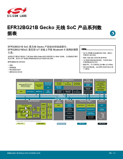
EFR32BG21B Gecko 无线 SoC 产品系列数据表EFR32BG21B SoC 是无线 Gecko 产品组合的组成部分。
EFR32BG21BSoC 是实现 IoT 设备上节能 Bluetooth 5 连网的理想之选。
这款单芯片解决方案结合了 80 MHz ARM Cortex-M33 和高性能 2.4 GHz 无线电,以及集成的 硬件安全引擎,旨在为 IoT 连接应用提供高度安全且节能的无线 SoC 。
EFR32BG21B 应用包括:主要特点•32 位 ARM® Cortex®-M33 内核,最高工作频率为 80 MHz•最高 1024 kB 闪存和 96 kB RAM •12 信道外围设备反射系统,可实现 MCU 外围设备的自主交互•集成 PA ,TX 功率高达 20 dBm (2.4 GHz)•强大的外围设备,4x4 QFN 封装内多达 20个 GPIO•照明•联网家庭•网关和数字助手•建筑自动化及安全EM4—ShutoffEM3—StopEM2—Deep SleepEM1—SleepEM0—Active| Building a more connected world.Rev. 1.01. 功能列表下方列出了 EFR32BG21B 的特色功能。
•低功耗无线片上系统•高性能 32 位 80 MHz ARM Cortex®-M33,带有 DSP 指令和浮点单元,可高效处理信号•高达 1024 kB 的闪存程序存储器•高达 96 kB 的 RAM 数据存储器•2.4 GHz 无线电操作•TX 功耗高达 20 dBm•低能耗•8.8 2.4 GHz 时 mA RX 电流 (1 Mbps GFSK)•9.32.4 GHz 和 0 dBm 输出功率时 mA TX 电流•33.8 2.4 GHz 和 10 dBm 输出功率时 mA TX 电流•50.9 主动模式 (EM0) 下 μA/MHz•5.0 μA EM2 深度睡眠电流(96 kB RAM 保留和通过 LFRCO 运行的 RTC)•4.5 μA EM2 深度睡眠电流(16 kB RAM 保留和通过 LFRCO 运行的 RTC)•高接收器性能•-97.5 dBm 灵敏度 @ 1 Mbit/s GFSK•-94.4 dBm 灵敏度 @ 2 Mbit/s GFSK•-104.9 dBm 灵敏度 @ 125 kbps GFSK•支持的调制格式•GFSK•协议支持•蓝牙低功耗 (Bluetooth 5)•可广泛选择的 MCU 外围设备•12 位 1 Msps SAR 模数转换器 (ADC)•2 个模拟比较器 (ACMP)•最多 20 个通用 I/O 引脚,具有输出状态保持和异步中断功能•8 信道 DMA 控制器•12 信道外围反射系统 (PRS)•3 个 16 位定时器/计数器•3 个比较/捕获/PWM 信道•1 个 32 位定时器/计数器•3 个比较/捕获/PWM 信道•32 位实时计数器•24 位低功耗定时器,用于产生波形•2 个看门狗定时器•3 个通用同步/异步接收器/发送器 (UART/SPI/SmartCard(ISO 7816)/IrDA/I2S)•2 个 I2C 接口,支持 SMBus•广泛的工作范围•1.71 V 至 3.8 V 单电源•-40°C 至 125°C 环境温度•Secure Vault•AES128/192/256、ChaCha20-Poly1305、SHA-1、SHA-2/256/384/512、ECDSA+ECDH(P-192、P-256、P-384、P-521)、Ed25519 和 Curve25519、J-PAKE、PBKDF2 的硬件加密加速•真随机数发生器 (TRNG)•ARM® TrustZone®•安全启动(根信任安全加载程序)•全调试解锁•DPA 对策•使用 PUF 进行安全密钥管理•防篡改•安全证明•QFN32 4x4 mm 封装•0.4 mm 间距EFR32BG21B Gecko 无线 SoC 产品系列数据表功能列表EFR32BG21B Gecko Wireless SoC Family Data SheetOrdering Information 2. Ordering InformationTable 2.1. Ordering Information | Building a more connected world.Rev. 1.0 | 3Table of Contents1. Feature List (2)2. Ordering Information (3)3. System Overview (7)3.1 Introduction (7)3.2 Radio (7)3.2.1 Antenna Interface (7)3.2.2 Fractional-N Frequency Synthesizer (8)3.2.3 Receiver Architecture (8)3.2.4 Transmitter Architecture (8)3.2.5 Packet and State Trace (8)3.2.6 Data Buffering (8)3.2.7 Radio Controller (RAC) (8)3.3 General Purpose Input/Output (GPIO) (9)3.4 Clocking (9)3.4.1 Clock Management Unit (CMU) (9)3.4.2 Internal and External Oscillators (9)3.5 Counters/Timers and PWM (9)3.5.1 Timer/Counter (TIMER) (9)3.5.2 Low Energy Timer (LETIMER) (9)3.5.3 Real Time Clock with Capture (RTCC) (10)3.5.4 Back-Up Real Time Counter (BURTC) (10)3.5.5 Watchdog Timer (WDOG) (10)3.6 Communications and Other Digital Peripherals (10)3.6.1 Universal Synchronous/Asynchronous Receiver/Transmitter (USART) (10)3.6.2 Inter-Integrated Circuit Interface (I2C) (10)3.6.3 Peripheral Reflex System (PRS) (10)3.7 Secure Vault High Features (10)3.7.1 Secure Boot with Root of Trust and Secure Loader (RTSL) (11)3.7.2 Cryptographic Accelerator (11)3.7.3 True Random Number Generator (11)3.7.4 Secure Debug with Lock/Unlock (11)3.7.5 DPA Countermeasures (11)3.7.6 Secure Key Management with PUF (12)3.7.7 Anti-Tamper (12)3.7.8 Secure Attestation (12)3.8 Analog (12)3.8.1 Analog Comparator (ACMP) (12)3.8.2 Analog to Digital Converter (IADC) (12)3.9 Reset Management Unit (RMU) (12)3.10 Core and Memory (13)3.10.1 Processor Core (13)3.10.2 Memory System Controller (MSC) (13)3.10.3 Linked Direct Memory Access Controller (LDMA) (13)3.11 Memory Map (14)3.12 Configuration Summary (15)4. Electrical Specifications (16)4.1 Electrical Characteristics (16)4.1.1 Absolute Maximum Ratings (17)4.1.2 General Operating Conditions (18)4.1.3 Thermal Characteristics (19)4.1.4 Current Consumption (20)4.1.5 2.4 GHz RF Transceiver Characteristics (25)4.1.6 Flash Characteristics (38)4.1.7 Wake Up, Entry, and Exit times (39)4.1.8 Oscillators (40)4.1.9 GPIO Pins (3V GPIO pins) (45)4.1.10 Analog to Digital Converter (ADC) (46)4.1.11 Analog Comparator (ACMP) (48)4.1.12 Temperature Sense (49)4.1.13 Brown Out Detectors (50)4.1.14 USART SPI Master Timing (52)4.1.15 USART SPI Slave Timing (54)4.1.16 I2C Electrical Specifications (55)4.1.17 Boot Timing (57)4.1.18 Crypto Operation Timing for SE Manager API (58)4.1.19 Crypto Operation Average Current for SE Manager API (60)4.2 Typical Performance Curves (62)4.2.1 Supply Current (63)4.2.2 2.4 GHz Radio (65)5. Typical Connection Diagrams (67)5.1 Power (67)5.2 RF Matching Networks (67)5.2.1 2.4 GHz 0 dBm Matching Network (68)5.2.2 2.4 GHz 10 dBm Matching Network (69)5.2.3 2.4 GHz 20 dBm Matching Network (69)5.3 Other Connections (70)6. Pin Definitions (71)6.1 QFN32 2.4GHz Device Pinout (71)6.2 Alternate Function Table (72)6.3 Analog Peripheral Connectivity (73)6.4 Digital Peripheral Connectivity (74)7. QFN32 Package Specifications (77)7.1 QFN32 Package Dimensions (77)7.2 QFN32 PCB Land Pattern (79)7.3 QFN32 Package Marking (81)8. Revision History (82)3. System Overview3.1 IntroductionThe EFR32 product family combines an energy-friendly MCU with a high performance radio transceiver. The devices are well suited for secure connected IoT multiprotocol devices requiring high performance and low energy consumption. This section gives a short intro-duction to the full radio and MCU system. The detailed functional description can be found in the EFR32xG21 Reference Manual.A block diagram of the EFR32BG21B family is shown in Figure 3.1 Detailed EFR32BG21B Block Diagram on page 7. The diagram shows a superset of features available on the family, which vary by OPN. For more information about specific device features, consult Ordering Information .RESETnDVDDAVDD PAVDD RFVDD DECOUPLEIOVDD PDnPCnPBnPAnRF2G4_IO1RF2G4_IO2Figure 3.1. Detailed EFR32BG21B Block Diagram3.2 RadioThe EFR32BG21B features a highly configurable radio transceiver supporting the Bluetooth Low Energy wireless protocol.3.2.1 Antenna InterfaceThe 2.4 GHz antenna interface consists of two single-ended pins (RF2G4_IO1 and RF2G4_IO2) that interface directly to two LNAs and two 10 dBm PAs. For devices that support 20 dBm, these pins also interface to the 20 dBm on-chip balun. Integrated switches select either RF2G4_IO1 or RF2G4_IO2 to be the active path.The external components and power supply connections for the antenna interface typical applications are shown in the RF Matching Networks section.Rev. 1.0 | 73.2.2 Fractional-N Frequency SynthesizerThe EFR32BG21B contains a high performance, low phase noise, fully integrated fractional-N frequency synthesizer. The synthesizer is used in receive mode to generate the LO frequency for the down-conversion mixer. It is also used in transmit mode to directly gener-ate the modulated RF carrier.The fractional-N architecture provides excellent phase noise performance, frequency resolution better than 100 Hz, and low energy consumption. The synthesizer’s fast frequency settling allows for very short receiver and transmitter wake up times to reduce system energy consumption.3.2.3 Receiver ArchitectureThe EFR32BG21B uses a low-IF receiver architecture, consisting of a Low-Noise Amplifier (LNA) followed by an I/Q down-conversion mixer. The I/Q signals are further filtered and amplified before being sampled by the IF analog-to-digital converter (IFADC).The IF frequency is configurable from 150 kHz to 1371 kHz. The IF can further be configured for high-side or low-side injection, provid-ing flexibility with respect to known interferers at the image frequency.The Automatic Gain Control (AGC) module adjusts the receiver gain to optimize performance and avoid saturation for excellent selec-tivity and blocking performance. The 2.4 GHz radio is calibrated at production to improve image rejection performance.Demodulation is performed in the digital domain. The demodulator performs configurable decimation and channel filtering to allow re-ceive bandwidths ranging from 0.1 to 2530 kHz. High carrier frequency and baud rate offsets are tolerated by active estimation and compensation. Advanced features supporting high quality communication under adverse conditions include forward error correction by block and convolutional coding as well as Direct Sequence Spread Spectrum (DSSS).A Received Signal Strength Indicator (RSSI) is available for signal quality metrics, for level-based proximity detection, and for RF chan-nel access by Collision Avoidance (CA) or Listen Before Talk (LBT) algorithms. An RSSI capture value is associated with each received frame and the dynamic RSSI measurement can be monitored throughout reception.3.2.4 Transmitter ArchitectureThe EFR32BG21B uses a direct-conversion transmitter architecture. For constant envelope modulation formats, the modulator controls phase and frequency modulation in the frequency synthesizer. Transmit symbols or chips are optionally shaped by a digital shaping filter. The shaping filter is fully configurable, including the BT product, and can be used to implement Gaussian or Raised Cosine shap-ing.Carrier Sense Multiple Access - Collision Avoidance (CSMA-CA) or Listen Before Talk (LBT) algorithms can be automatically timed by the EFR32BG21B. These algorithms are typically defined by regulatory standards to improve inter-operability in a given bandwidth be-tween devices that otherwise lack synchronized RF channel access.3.2.5 Packet and State TraceThe EFR32BG21B Frame Controller has a packet and state trace unit that provides valuable information during the development phase. It features:•Non-intrusive trace of transmit data, receive data and state information•Data observability on a single-pin UART data output, or on a two-pin SPI data output•Configurable data output bitrate / baudrate•Multiplexed transmitted data, received data and state / meta information in a single serial data stream3.2.6 Data BufferingThe EFR32BG21B features an advanced Radio Buffer Controller (BUFC) capable of handling up to 4 buffers of adjustable size from 64 bytes to 4096 bytes. Each buffer can be used for RX, TX or both. The buffer data is located in RAM, enabling zero-copy operations.3.2.7 Radio Controller (RAC)The Radio Controller controls the top level state of the radio subsystem in the EFR32BG21B. It performs the following tasks:•Precisely-timed control of enabling and disabling of the receiver and transmitter circuitry•Run-time calibration of receiver, transmitter and frequency synthesizer•Detailed frame transmission timing, including optional LBT or CSMA-CA3.3 General Purpose Input/Output (GPIO)EFR32BG21B has up to 20 General Purpose Input/Output pins. Each GPIO pin can be individually configured as either an output or input. More advanced configurations including open-drain, open-source, and glitch-filtering can be configured for each individual GPIO pin. The GPIO pins can be overridden by peripheral connections, like SPI communication. Each peripheral connection can be routed to several GPIO pins on the device. The input value of a GPIO pin can be routed through the Peripheral Reflex System to other peripher-als. The GPIO subsystem supports asynchronous external pin interrupts.All of the pins on ports A and port B are EM2 capable. These pins may be used by Low-Energy peripherals in EM2/3 and may also be used as EM2/3 pin wake-ups. Pins on ports C and D are latched/retained in their current state when entering EM2 until EM2 exit upon which internal peripherals could once again drive those pads.A few GPIOs also have EM4 wake functionality. These pins are listed in .3.4 Clocking3.4.1 Clock Management Unit (CMU)The Clock Management Unit controls oscillators and clocks in the EFR32BG21B. Individual enabling and disabling of clocks to all pe-ripheral modules is performed by the CMU. The CMU also controls enabling and configuration of the oscillators. A high degree of flexi-bility allows software to optimize energy consumption in any specific application by minimizing power dissipation in unused peripherals and oscillators.3.4.2 Internal and External OscillatorsThe EFR32BG21B supports two crystal oscillators and fully integrates five RC oscillators, listed below.• A high frequency crystal oscillator (HFXO) with integrated load capacitors, tunable in small steps, provides a precise timing refer-ence for the MCU and RF synthesizer. The HFXO provides excellent RF clocking performance using a 38.4 MHz crystal. The HFXO can also support an external clock source such as a TCXO for applications that require an extremely accurate clock frequency over temperature.• A 32.768 kHz crystal oscillator (LFXO) provides an accurate timing reference for low energy modes.•An integrated high frequency RC oscillator (HFRCO) is available for the MCU system, when crystal accuracy is not required. The HFRCO employs fast start-up at minimal energy consumption combined with a wide frequency range, from 1 MHz to 80 MHz.•An integrated high frequency RC oscillator (HFRCOEM2) runs down to EM2 and is available for timing the general-purpose ADC and the Serial Wire Viewer port with a wide frequency range.•An integrated fast start-up RC oscillator (FSRCO) that runs at a fixed 20 MHz•An integrated low frequency 32.768 kHz RC oscillator (LFRCO) for low power operation where high accuracy is not required.•An integrated ultra-low frequency 1 kHz RC oscillator (ULFRCO) is available to provide a timing reference at the lowest energy con-sumption in low energy modes.3.5 Counters/Timers and PWM3.5.1 Timer/Counter (TIMER)TIMER peripherals keep track of timing, count events, generate PWM outputs and trigger timed actions in other peripherals through the Peripheral Reflex System (PRS). The core of each TIMER is a 16-bit or 32-bit counter with up to 3 compare/capture channels. Each channel is configurable in one of three modes. In capture mode, the counter state is stored in a buffer at a selected input event. In compare mode, the channel output reflects the comparison of the counter to a programmed threshold value. In PWM mode, the TIMER supports generation of pulse-width modulation (PWM) outputs of arbitrary waveforms defined by the sequence of values written to the compare registers. In addition some timers offer dead-time insertion.See 3.12 Configuration Summary for information on the feature set of each timer.3.5.2 Low Energy Timer (LETIMER)The unique LETIMER is a 24-bit timer that is available in energy mode EM0 Active, EM1 Sleep, EM2 Deep Sleep, and EM3 Stop. This allows it to be used for timing and output generation when most of the device is powered down, allowing simple tasks to be performed while the power consumption of the system is kept at an absolute minimum. The LETIMER can be used to output a variety of wave-forms with minimal software intervention. The LETIMER is connected to the Peripheral Reflex System (PRS), and can be configured to start counting on compare matches from other peripherals such as the Real Time Clock.3.5.3 Real Time Clock with Capture (RTCC)The Real Time Clock with Capture (RTCC) is a 32-bit counter providing timekeeping down to EM3. The RTCC can be clocked by any of the on-board low-frequency oscillators, and it is capable of providing system wake-up at user defined intervals.A secondary RTC is used by the RF protocol stack for event scheduling, leaving the primary RTCC block available exclusively for appli-cation software.3.5.4 Back-Up Real Time Counter (BURTC)The Back-Up Real Time Counter (BURTC) is a 32-bit counter providing timekeeping in all energy modes, including EM4. The BURTC can be clocked by any of the on-board low-frequency oscillators, and it is capable of providing system wake-up at user defined inver-vals.3.5.5 Watchdog Timer (WDOG)The watchdog timer can act both as an independent watchdog or as a watchdog synchronous with the CPU clock. It has windowed monitoring capabilities, and can generate a reset or different interrupts depending on the failure mode of the system. The watchdog can also monitor autonomous systems driven by the Peripheral Reflex System (PRS).3.6 Communications and Other Digital Peripherals3.6.1 Universal Synchronous/Asynchronous Receiver/Transmitter (USART)The Universal Synchronous/Asynchronous Receiver/Transmitter is a flexible serial I/O module. It supports full duplex asynchronous UART communication with hardware flow control as well as RS-485, SPI, MicroWire and 3-wire. It can also interface with devices sup-porting:•ISO7816 SmartCards•IrDA•I2S3.6.2 Inter-Integrated Circuit Interface (I2C)The I2C module provides an interface between the MCU and a serial I2C bus. It is capable of acting as both a master and a slave and supports multi-master buses. Standard-mode, fast-mode and fast-mode plus speeds are supported, allowing transmission rates from 10 kbit/s up to 1 Mbit/s. Slave arbitration and timeouts are also available, allowing implementation of an SMBus-compliant system. The interface provided to software by the I2C module allows precise timing control of the transmission process and highly automated trans-fers. Automatic recognition of slave addresses is provided in active and low energy modes. Note that not all instances of I2C are avalia-ble in all energy modes.3.6.3 Peripheral Reflex System (PRS)The Peripheral Reflex System provides a communication network between different peripheral modules without software involvement. Peripheral modules producing Reflex signals are called producers. The PRS routes Reflex signals from producers to consumer periph-erals which in turn perform actions in response. Edge triggers and other functionality such as simple logic operations (AND, OR, NOT) can be applied by the PRS to the signals. The PRS allows peripherals to act autonomously without waking the MCU core, saving pow-er.3.7 Secure Vault High FeaturesA dedicated Hardware Secure Engine containing its own CPU enables the Secure Vault High functions. It isolates cryptographic func-tions and data from the host Cortex-M33 core and provides the following security features:•Secure Boot with Root of Trust and Secure Loader (RTSL)•Cryptographic Accelerator•True Random Number Generator (TRNG)•Secure Debug with Lock/Unlock•DPA Countermeasures•Secure Key Management with PUF•Anti-Tamper•Secure Attestation3.7.1 Secure Boot with Root of Trust and Secure Loader (RTSL)The Secure Boot with RTSL authenticates a chain of trusted firmware that begins from an immutable memory (ROM).It prevents malware injection, prevents rollback, ensures that only authentic firmware is executed and protects Over The Air updates. More information on this feature can be found in the Application Note AN1218: Series 2 Secure Boot with RTSL.3.7.2 Cryptographic AcceleratorThe Cryptographic Accelerator is an autonomous hardware accelerator with Differential Power Analysis (DPA) countermeasures to pro-tect keys.It supports AES encryption and decryption with 128/192/256-bit keys, ChaCha20 encryption, and Elliptic Curve Cryptography (ECC) to support public key operations and hashes.Supported block cipher modes of operation for AES include:•ECB (Electronic Code Book)•CTR (Counter Mode)•CBC (Cipher Block Chaining)•CFB (Cipher Feedback)•GCM (Galois Counter Mode)•CCM (Counter with CBC-MAC)•CBC-MAC (Cipher Block Chaining Message Authentication Code)•GMAC (Galois Message Authentication Code)The Cryptographic Accelerator accelerates Elliptical Curve Cryptography and supports the NIST (National Institute of Standards and Technology) recommended curves including P-192, P-256, P-384, and P-521 for ECDH (Elliptic Curve Diffie-Hellman) key derivation and ECDSA (Elliptic Curve Digital Signature Algorithm) sign and verify operations. Also supported is the non-NIST Curve25519 for ECDH and Ed25519 for EdDSA (Edwards-curve Digital Signature Algorithm) sign and verify operations.Secure Vault also supports ECJ-PAKE (Elliptic Curve variant of Password Authenticated Key Exchange by Juggling) and PBKDF2 (Password-Based Key Derivation Function 2).Supported hashes include SHA-1, SHA-2/256/384/512 and Poly1305.This implementation provides a fast and energy efficient solution to state of the art cryptographic needs.3.7.3 True Random Number GeneratorThe True Random Number Generator module is a non-deterministic random number generator that harvests entropy from a thermal energy source. It includes start-up health tests for the entropy source as required by NIST SP800-90B and AIS-31 as well as online health tests required for NIST SP800-90C.The TRNG is suitable for periodically generating entropy to seed an approved pseudo random number generator.3.7.4 Secure Debug with Lock/UnlockFor obvious security reasons, it is critical for a product to have its debug interface locked before being released in the field.In addition, Secure Vault High also provides a secure debug unlock function that allows authenticated access based on public key cryp-tography. This functionality is particularly useful for supporting failure analysis while maintaining confidentiality of IP and sensitive end-user data.More information on this feature can be found in the Application Note AN1190: Series 2 Secure Debug.3.7.5 DPA CountermeasuresThe AES and ECC accelerators have Differential Power Analysis (DPA) countermeasures support. This makes it very expensive from a time and effort standpoint to use DPA to recover secret keys.3.7.6 Secure Key Management with PUFKey material in Secure Vault High products is protected by what is called "key wrapping" with a standardized symmetric encryption mechanism. This method has the advantage of being able to protect a virtually unlimited number of keys, limited only by the storage that is accessible by the Cortex-M33 (which includes off-chip storage as well). The symmetric key used for this wrapping and unwrap-ping must be highly secure as it can expose all other key material in the system. The Secure Vault Key Management system uses a Physically Unclonable Function (PUF) to generate a persistent device-unique seed key on power up to dynamically generate this critical wrapping/unwrapping key which is only visible to the AES encryption engine and is not retained when the device loses power.3.7.7 Anti-TamperSecure Vault High devices provide internal tampers monitoring the system such as voltage, temperature, and electro-mechanical pul-ses as well as detecting tamper of the security sub-system itself. There are also 8 external configurable tamper pins for supporting ex-ternal tamper sources like case tamper switches.For each tamper event, the user is able to select the severity of the tamper response ranging from an interrupt, to a reset, to destroying the PUF reconstruction data which will make all the protected key material un-recoverable and effectively render the device inoperable. The tamper system also has an internal resettable event counter with programmable trigger threshold and refresh periods to mitigate false positive tamper events.More information on this feature can be found in the Application Note AN1247: Anti-Tamper Protection Configuration and Use.3.7.8 Secure AttestationSecure Vault High products support Secure Attestation, which begins with a secure identity that is created during the Silicon Labs man-ufacturing process. During device production, each device generates its own public/private keypair and securely stores the wrapped private key into immutable OTP memory, and this key never leaves the device. The corresponding public key is extracted from the de-vice and inserted into a binary DER-encoded X.509 device certificate which is signed into a Silicon Labs CA chain and then program-med back into the chip into an immutable OTP memory.This secure identity can be used to authenticate the chip at any time in the life of the product. The production certification chain can be requested remotely from the product. This certification chain can be used to verify that the device was authentically produced by Silicon Labs. The device unique public key is also bound to the device certificate in the certification chain. A challenge can be sent to the chip at any point in time to be signed by the device private key. The public key in the device certificate can then be used to verify the chal-lenge response, proving that the device has access to the securely-stored private key, which prevents counterfeit products or imperso-nation attacks.More information on this feature can be found in the Application Note AN1268: Authenticating Silicon Labs Devices Using Device Certif-icates.3.8 Analog3.8.1 Analog Comparator (ACMP)The Analog Comparator is used to compare the voltage of two analog inputs, with a digital output indicating which input voltage is high-er. Inputs are selected from among internal references and external pins. The tradeoff between response time and current consumption is configurable by software. Two 6-bit reference dividers allow for a wide range of internally-programmable reference sources. The ACMP can also be used to monitor the supply voltage. An interrupt can be generated when the supply falls below or rises above the programmable threshold.3.8.2 Analog to Digital Converter (IADC)The IADC is a hybrid architecture combining techniques from both SAR and Delta-Sigma style converters. It has a resolution of up to 12 bits at up to 1 Msps. Hardware oversampling reduces system-level noise over multiple front-end samples. The IADC includes integrated voltage references. Inputs are selectable from a wide range of sources, including pins configurable as either single-ended or differential.3.9 Reset Management Unit (RMU)The RMU is responsible for handling reset of the EFR32BG21B. A wide range of reset sources are available, including several power supply monitors, pin reset, software controlled reset, core lockup reset, and watchdog reset.3.10 Core and Memory3.10.1 Processor CoreThe ARM Cortex-M processor includes a 32-bit RISC processor integrating the following features and tasks in the system:•ARM Cortex-M33 RISC processor achieving 1.50 Dhrystone MIPS/MHz•ARM TrustZone security technology•Embedded Trace Macrocell (ETM) for real-time trace and debug•Up to 1024 kB flash program memory•Up to 96 kB RAM data memory•Configuration and event handling of all modules•2-pin Serial-Wire debug interface3.10.2 Memory System Controller (MSC)The Memory System Controller (MSC) is the program memory unit of the microcontroller. The flash memory is readable and writable from both the Cortex-M and DMA. In addition to the main flash array where Program code is normally written the MSC also provides an Information block where additional information such as special user information or flash-lock bits are stored. There is also a read-only page in the information block containing system and device calibration data. Read and write operations are supported in energy modes EM0 Active and EM1 Sleep.3.10.3 Linked Direct Memory Access Controller (LDMA)The Linked Direct Memory Access (LDMA) controller allows the system to perform memory operations independently of software. This reduces both energy consumption and software workload. The LDMA allows operations to be linked together and staged, enabling so-phisticated operations to be implemented.。
上海富芮坤:部署CEVA低功耗蓝牙IP

上海富芮坤:部署CEVA低功耗蓝牙IPCEVA,全球领先的智能和互连设备的信号处理IP 授权许可厂商宣布,上海富芮坤微电子有限公司(Freqchip)已经获得授权许可,在其最新FR801x 无线芯片(IC)系列中部署CEVA 的RivieraWaves 低功耗蓝牙技术。
FR8010 以富芮坤成熟的低功耗无线IC 设计专业技术为基础,是FR801X 系列的首款成员,是各种需要蓝牙的消费类产品的理想之选芯片,包括个人健康和健身可穿戴产品,以及智能家用电器。
下面就随单片机小编一起来了解一下相关内容吧。
蓝牙:是一种无线技术标准,可实现固定设备、移动设备和楼宇个人域网之间的短距离数据交换(使用2.4—2.485GHz 的ISM 波段的UHF 无线电波)。
上海富芮坤:部署CEVA 低功耗蓝牙IPCEVA,全球领先的智能和互连设备的信号处理IP 授权许可厂商宣布,上海富芮坤微电子有限公司(Freqchip)已经获得授权许可,在其最新FR801x 无线芯片(IC)系列中部署CEVA 的RivieraWaves 低功耗蓝牙技术。
FR8010 以富芮坤成熟的低功耗无线IC 设计专业技术为基础,是FR801X 系列的首款成员,是各种需要蓝牙的消费类产品的理想之选芯片,包括个人健康和健身可穿戴产品,以及智能家用电器。
上海富芮坤首席执行官黎传礼称:“蓝牙仍然是极低功耗电子器件在连接方面的主流选择。
CEVA 的RivieraWaves 低功耗蓝牙IP 获得各界广泛使用,并且在中国大规模量产,以超低功耗架构提供各种先进特性,且风险非常低,因此是我们的最理想选择。
”CEVA 连接性业务部门副总裁兼总经理Aviv Malinovitch 称:“我们很高兴宣布上海富芮坤微电子获授权使用我们的RivieraWaves 蓝牙IP。
FR8010 是令人耳目一新的低功耗器件,展示了这公司的工程设计传承,并为大规模量产的蓝。
蓝牙4.0技术公开课PPT_朱兆祺_第1章
无线广域网
Wireless Wide Area Network
图1. 四种无线网络的传输速度和传输距离对比
2.无线网络中的短距离通信
短距离
无线体域网
距离 <1m <10m <500m 20km~50km
表1. 短距离无线通信的发展过程与特点 标准或技术 推出时间 典型通信距离(m) 最大数据传输速率(Mbps)
定提交其低功耗技术。但是诺基亚的低功耗技术基于蓝牙并不受IEEE青睐,于是
指出诺基亚低功耗无线电仅仅作为一个独立的提案,缺乏跨公司的合作。 2004年中期,诺基亚通过改变标准蓝牙技术规范的设备发现、跳频、双模和单模, 实现了低功耗特性,并且完成了项目开发和演示系统,至此称之为蓝牙低端扩展 (Bluetooth low end extension)。但是当时的诺基亚还没有发现合适的机会进 行技术转让和应用,该技术前景一度暗淡。
“蓝牙”是一种开放的技术规范,它可在世界上的任何地方实现短距离的无线语 音和数据通信。 蓝牙的创始人是瑞典爱立信公司,爱立信早在1994年就已进行研发。1997年, 爱立信与其他设备生产商联系,并激发了他们对该项技术的浓厚兴趣。 1998年2月, 5个跨国大公司,包括爱立信、诺基亚、IBM、东芝及Intel组成了一个特殊兴趣小组 (Bluetooth Special Interest Group —— SIG),他们共同的目标是建立一个全
0.5~4s,传感器类应用程序发送的数据量较平常要少很多,而且所有连接均采用
先进的SSR(Sniff Sub-Rating)功能模式,因此此时的射频能耗几乎可以忽略不计, 综合以上因素,低功耗蓝牙的待机功耗较传统蓝牙大大减少。
c.传输距离、可靠性和安全性的提高
soc芯片ppt课件

外设接口设计
外设接口类型
选择合适的外设接口类型,如SPI、I2C、 UART等。
外设中断处理
实现外设中断的快速响应和处理。
外设驱动程序开发
编写外设驱动程序,实现外设与处理器核的 通信和控制。
外设时钟管理
对外设接口进行时钟管理,确保外设正常工 作。
03
CHAPTER
SOC芯片开发流程
需求分析
01
总结词
智能语音助手芯片是SOC芯片在智能语 音识别领域的应用,它能够实现高效、 准确的语音识别和语音合成,为智能语 音助手提供强大的技术支持。
VS
详细描述
智能语音助手芯片集成了高性能的语音信 号处理算法和人工智能技术,能够快速、 准确地识别用户的语音指令,并自动完成 相应的任务。它广泛应用于智能家居、智 能车载、智能客服等领域,为用户提供便 捷、高效的人机交互体验。
SOC芯片在通信领域中主要用于高速数据传输和处理,如路由器、交换机等设备中;在计算机领域中主要用于高 性能计算和数据中心等;在消费电子领域中主要用于智能手机、平板电脑等便携式设备中;在汽车电子领域中主 要用于车载娱乐系统、安全控制系统等。
SOC芯片的发展历程
总结词
SOC芯片的发展历程经历了从简单到复杂、从单一到多元的演变。
详细描述
SOC芯片是一种系统级芯片,它将多个功能模块集成在一个芯片上,实现了高 度的集成度和性能。相比传统的集成电路芯片,SOC芯片具有更低的功耗、更 高的性能和更小的体积,因此被广泛应用于各种领域。
SOC芯片的应用领域
总结词
SOC芯片在通信、计算机、消费电子、汽车电子等领域有着广泛的应用。
详细描述
多核协同工作
智能休眠与唤醒
互联网创新创业大赛项目案例课件
互联网创新创业大赛项目案例课件目录一、大赛背景及目的 (2)1.1 大赛背景介绍 (2)1.2 大赛目的与意义 (3)二、项目概述 (4)2.1 项目简介 (5)2.2 项目发起人与团队介绍 (6)三、案例展示 (7)3.1 项目案例一 (8)3.1.1 项目内容 (10)3.1.2 项目进展及成果 (11)3.1.3 项目特色与创新点 (12)3.2 项目案例二 (13)3.2.1 项目内容 (14)3.2.2 项目进展及成果 (16)3.2.3 项目特色与创新点分析 (17)四、创业方案与实施策略 (18)4.1 市场分析与定位 (19)4.2 产品研发与创新 (21)4.3 营销策略与渠道 (22)4.4 团队组建与管理体系 (23)五、项目挑战及解决方案 (25)5.1 技术难题及应对策略 (26)5.2 市场推广难题及解决方案 (27)5.3 人才流失风险及应对措施 (28)六、项目发展前景展望 (29)6.1 行业发展趋势分析 (30)6.2 项目未来规划与目标 (31)6.3 项目社会价值与经济效益预测 (32)七、评委点评及建议反馈汇总分析 (34)一、大赛背景及目的随着互联网技术的飞速发展,互联网产业已经成为全球经济发展的重要引擎。
为了推动互联网创新创业,培养具有创新精神和创业能力的人才,提高互联网产业的整体竞争力,各级政府、高校和企业纷纷举办各类互联网创新创业大赛。
这些大赛旨在激发广大青年学生的创新激情,为他们提供一个展示自己才华的平台,同时也为企业提供了一个寻找优秀项目和人才的机会。
1.1 大赛背景介绍随着互联网技术的迅速发展和普及,创新创业已成为推动时代发展的重要动力。
在这一背景下,互联网创新创业大赛应运而生,旨在为广大创新创业者提供一个展示项目、交流思想、获取资源和建立合作机会的平台。
本项目案例课件,针对互联网创新创业大赛背景进行深入解析。
在当前经济全球化的大背景下,互联网行业正在引领新一轮科技革命和产业变革,新的业态不断涌现,市场潜力巨大。
上海富芮坤获得CEVA低功耗蓝牙IP授权许可并部署IoT产品

上海富芮坤获得CEVA低功耗蓝牙IP授权许可并部署IoT产品集微网消息,全球领先的智能和互连设备的信号处理IP 授权许可厂商CEVA 宣布,上海富芮坤微电子有限公司(Freqchip)已经获得授权许可,在其最新FR801x 无线芯片(IC)系列中部署CEVA 的RivieraWaves 低功耗蓝牙技术。
FR8010 以富芮坤成熟的低功耗无线IC 设计专业技术为基础,是FR801X 系列的首款成员,是各种需要蓝牙的消费类产品的理想之选芯片,包括个人健康和健身可穿戴产品,以及智能家用电器。
上海富芮坤首席执行官黎传礼称:“蓝牙仍然是极低功耗电子器件在连接方面的主流选择。
CEVA 的RivieraWaves 低功耗蓝牙IP 获得各界广泛使用,并且在中国大规模量产,以超低功耗架构提供各种先进特性,且风险非常低,因此是我们的最理想选择。
”CEVA 连接性业务部门副总裁兼总经理Aviv Malinovitch 称:“我们很高兴宣布上海富芮坤微电子获授权使用我们的RivieraWaves 蓝牙IP。
FR8010 是令人耳目一新的低功耗器件,展示了这公司的工程设计传承,并为大规模量产的蓝牙消费类产品提供了一个出色解决方案。
”CEVA 的RivieraWaves 蓝牙IP 平台提供低功耗蓝牙和蓝牙双模通讯,由硬件基带控制器及拥有丰富功能特性的软件协议堆栈组成。
灵活的无线接口使该平台能够与RivieraWaves RF 或各合作伙伴的RF IP 一起部署,允许选择最合适的晶圆厂和工艺节点。
这个平台支持所有蓝牙5 的功能特性,包括低功耗2Mbps 数据率、远距离和低功耗广告扩展。
到目前为止,搭载RivieraWaves 蓝牙IP 的终端产品已经有10 多亿面市,有几十家厂商获得授权使用,广泛部署在许多世界领先的半导体公司和OEM 的消费类和IoT 器件中,包括智能手机、。
RFID_技术应用及案例分析 ppt课件

2021/3/26
RFID_技术应用及案例分析 ppt课
4
件
•应用领域概况
2021/3/26
RFID_技术应用及案例分析 ppt课
5
件
RFID_技术应用及案例分析
2021/3/26
RFID_技术应用及案例分析 ppt课
6
件
RFID_技术应用及案例分析
2021/3/26
RFID_技术应用及案例分析 ppt课
•
1. 快:物流效率快,货品交接点数快,提高物流作业效
率
•
2 .准:数据准,在供应链的各个环节对服装的流通数据
采集准确
•
3. 防:通过嵌入RFID芯片到服装内部,实现防窜货和防
伪功效,而且还提高物流效率。
•
4. 服务:通过RFID智能商店,提高消费者体验,通过互
动,更多商品的展示,快速响应消费者需求来
• 药品盘点:将药品的出厂单位、日期、药物类别等信 息存入RFID标签,然后在药品包装盒贴上RFID标签 ,盘点时通过手持式RFID读取器对药品标签进行信 息读取。可以有效查看药品是否过期以及检查药品库 存数量。
2021/3/26
RFID_技术应用及案例分析 ppt课
24
件
RFID_技术应用购及药案流例程分图析示
计划,许多高科技公司也正在开发RFID专用的软件和硬件,
这些公司包括英特尔,微软,甲骨文和SUN等。ABI估计,
RFID技术市场在未来五年内将有数万亿美元的市场空间。
2021/3/26
RFID_技术应用及案例分析 ppt课
30
件
•
到二十一世纪初,RFID迎来了一个崭新的发
展时期,其在民用领域的价值开始得到世界各国的
SoC设计流程优质PPT课件
基于标准单元的SoC芯片设计流程
• 单元布局和优化(Placement &
Optimization)
单元布局和优化主要定义每个标准单元的摆放位置并根 据摆放的位置进行优化。
• 静态时序分析(STA,Static Timing
• 前仿真(Pre-layout Simulation)
前仿真也叫RTL级仿真。通过HDL仿真器验证电路逻辑 功能是否有效。在前仿真时,通常与具体的电路物理实 现无关,没有时序信息。
基于标准单元的SoC芯片设计流程
• 逻辑综合(Logic Synthesis)
逻辑综合是指使用EDA工具把由硬件描述语言设计的电 路自动转换成特定工艺下的网表,即从RTL级的HDL描 述通过编译与优化产生符合约束条件的门级网表。
软件和硬件实现的优缺点
内容大纲
• SoC设计的特点 • 软硬件协同设计 • 基于标准单元的SoC芯片设计流程
基于标准单元的SoC芯片设计流程
• 硬件设计定义说明(Hardware Design
Specification)
硬件设计定义说明描述芯片总体结构、规格参数、模块 划分、使用的总线,以及各个模块的详细定义等。
Order)
ECO修改是工程修改命令的意思。
这一步实际上是正常设计流程的一个例外。当在设计的 最后阶段发现个别路径有时序问题或逻辑错误时,有必 要通过ECO对设计的局部进行小范围的修改和重新布线 ,并不影响芯片其余部分的布局布线。在大规模的IC设 计中,ECO修改是一种有效、省时的方法,通常会被采 用。
基于标准单元的SoC芯片设计流程
• 物理验证(Physical Verification)
超深亚微米SOC芯片的低功耗后端设计的开题报告
超深亚微米SOC芯片的低功耗后端设计的开题报告一、选题背景和意义近年来,随着移动终端、物联网、云计算等技术的快速发展,计算机系统对功耗、性能和功能的要求变得越来越高。
尤其是在移动终端领域,用户对续航能力和低功耗的需求不断提升。
为了满足这些需求,SOC (System on Chip,片上系统)芯片的设计成为了必不可少的一环。
SOC芯片在细节方面有着诸多考虑,其中之一就是后端设计。
后端设计不仅决定了芯片的功耗、面积和时序性能,还会直接影响到芯片的设计周期和成本。
对于超深亚微米SOC芯片,更是需要考虑工艺、设备、信噪比等问题,这都将对后端设计带来更大的挑战。
因此,本文拟以超深亚微米SOC芯片的低功耗后端设计为研究方向,探索如何在后端设计中实现低功耗、高性能和低成本的平衡,以及如何有效地解决面对超深亚微米SOC芯片的各种问题。
二、研究内容和方法本文将以超深亚微米SOC芯片的低功耗后端设计作为研究内容,主要包括以下几个方面:1.低功耗逻辑综合:低功耗逻辑综合是实现超深亚微米SOC芯片低功耗的关键。
本文将研究低功耗逻辑综合的原理和实现方法,探索如何在保证逻辑功能正确的前提下,尽可能地降低功耗。
2.低功耗物理设计:低功耗物理设计是后端设计中一个重要的环节,它决定了芯片的面积和功耗。
本文将研究低功耗物理设计中的各种技术和算法,探索如何降低功耗、减小芯片面积和提高性能。
3.时序约束:在超深亚微米工艺下,时序约束会面临更大的挑战,因此本文将研究如何针对超深亚微米SOC芯片的工艺特点设计出合理的时序约束,保证芯片能够在各种复杂场景下正常运行。
4.DRC和LVS:DRC和LVS是后端设计中一项重要的检查工具,用于检查芯片设计是否符合工艺规则和逻辑规则。
本文将研究如何有效地使用DRC和LVS工具,规避后端设计中的各种缺陷。
本文将采用理论研究、仿真实验和工程实践相结合的方法进行研究。
通过对不同方法的对比与评估,力求找到最佳的方案,并运用到实际的超深亚微米SOC芯片设计中。
乐鑫 ESP32-C3 系列芯片 技术规格书说明书
技术规格书
搭载 RISC-V 32 位单核处理器的极低功耗 SoC 支持 2.4 GHz Wi-Fi (802.11 b/g/n) 和 Bluetooth® 5 (LE) 封装内可叠封 4 MB flash QFN32 (5×5 mm) 封装
包括:
ESP32-C3 ESP32-C3FN4 – 不推荐用于新设计 (NRND) ESP32-C3FH4 ESP32-C3FH4AZ
乐鑫信息科技
4 反馈文档意见
ESP32-C3 系列芯片技术规格书 v1.5
安全机制
• 安全启动 - 内部和外部存储器的权限控制 • Flash 加密 - 加密和解密存储器 • 4096 位 OTP,用户可用的高达 1792 位 • 加密硬件加速器:
– AES-128/256 (FIPS PUB 197) – SHA 加速器 (FIPS PUB 180-4) – RSA 加速器 – 随机数生成器 (RNG) – HMAC – 数字签名
I2S
TWAI® Debug Assistant
Peripherals
Generalpurpose Timers
LED PWM
System Timer
GPIO
eFuse Controller
DIG ADC
Temperature Sensor
USB Serial/ JTAG
Main System Watchdog Timers
功耗管理
• 通过选择时钟频率、占空比、Wi-Fi 工作模式和单独控制内部器件的电源,实现精准电源控制 • 针对典型场景设计的四种功耗模式:Active、Modem-sleep、Light-sleep、Deep-sleep • Deep-sleep 模式下功耗低至 5 µA • Deep-sleep 模式下 RTC 存储器仍保持工作
蓝牙技术答辩ppt
► 专业:测控技术与仪器 ► 年级:xxxx 年级:xxxx ► 学院:xxxxx 学院:xxxxx ► 指导老师:xxxxx 指导老师:xxxxx
► 主讲人:xxxx 主讲人:xxxx
蓝牙应用简介
►1
蓝牙的由来
蓝牙(Bluetooth)是--种低功率、短距离的无线通信技术 蓝牙(Bluetooth)是--种低功率、短距离的无线通信技术 标准的代称,“蓝牙"一词取自于一位在公元10世纪统一了 标准的代称,“蓝牙"一词取自于一位在公元10世纪统一了 丹麦的国王哈拉德二世(Harald)的绰号。蓝牙技术的最初倡 丹麦的国王哈拉德二世(Harald)的绰号。蓝牙技术的最初倡 导者是五家世界著名的计算机和通信公司:爱立信Ericsson、 导者是五家世界著名的计算机和通信公司:爱立信Ericsson、 国际商用机器IBM、英特尔Intel、诺基亚NoKIA和东芝 国际商用机器IBM、英特尔Intel、诺基亚NoKIA和东芝 Toshiba。1998年 月,以爱立信为首,此五家IT巨人共同提 Toshiba。1998年5月,以爱立信为首,此五家IT巨人共同提 出了一种近距离无线数字通信的技术标准,目标是实现最高 传输速率可达1Mb/s(有效传输速率为720Kb/s),最大传输 传输速率可达1Mb/s(有效传输速率为720Kb/s),最大传输 距离为10m的无线通信技术,即蓝牙技术,并成立了国际化 距离为10m的无线通信技术,即蓝牙技术,并成立了国际化 组织蓝牙SIG(SpecialInterest Group),致力于蓝牙规范的制定 组织蓝牙SIG(SpecialInterest Group),致力于蓝牙规范的制定 和蓝牙技术在全球范围内的推广。
成本的无线互联通讯。
- 1、下载文档前请自行甄别文档内容的完整性,平台不提供额外的编辑、内容补充、找答案等附加服务。
- 2、"仅部分预览"的文档,不可在线预览部分如存在完整性等问题,可反馈申请退款(可完整预览的文档不适用该条件!)。
- 3、如文档侵犯您的权益,请联系客服反馈,我们会尽快为您处理(人工客服工作时间:9:00-18:30)。
市场 容量 蓝牙耳机市场规模 650KK/年(月均近54KK)
蓝牙智能SoC 是IOT 产业的基础支撑技术
© 2015 All Rights Reserved CONFIDENTIAL
项目建设内容
蓝牙BLE SoC 是智能物联网芯片的重要表现形式之一,本项目“超低功耗 蓝牙无线SOC芯片”是基于BT4.2/BLE标准协议规范,设计出国内第一 款低功耗、短距离、低成本、高可靠性的无线通信SOC芯片。
芯片集成度高,包括射频RF,处理器,外设,通信编解码模块,通信基带,内存, eflash,以及应用层协议栈,可以根据不同市场产品的需求集成在同一颗芯片上, 功耗低,技术含量高;。
© 2015 All Rights Reserved CONFIDENTIAL
BLEHomeKit
BLE-iBeacon
BLEHealthKit
BLE-Sport
BLE-Wearable
BLE-wireless charging
项目概述
► 行业介绍
随着手持数码设备的增多,由于蓝牙无线连接的普遍性,所以备受关注;蓝牙4.0版本支持省电+长距离传输,使得 蓝牙产品应用起来更加广泛。 “蓝牙技术”是一种开放的技术规范,它可实现短距离的无线语音和数据通信。这一技术是由爱立信移动通信公司 1994年开始首先发起并且联合诺基亚(Nokia)、英特尔(Intel)、IBM 、东芝(Toshiba)等七家公司一起成立 了蓝牙国际联盟(Special Interest Group,SIG),负责蓝牙技术标准的制定、产品测试,并协调各国蓝牙的具体 使用。SIG 着眼于蓝牙在全球的发展与应用,并且将蓝牙技术标准完全公开。目前,蓝牙SIG组织已经有超过3000 多家会员,并且几乎覆盖了全球各行各业,蓝牙技术也广泛应用于手机、平板电脑、PC、无线耳机、无线音箱以及 键盘、鼠标等各种电子设备中。
► 总体概述
本公司自主研发的 “超低功耗蓝牙SOC芯片”是一颗和低功耗蓝牙(BLE)协议完全兼容的无线传输单芯片(SOC ),主要应用智能家庭,物联网,穿戴式设备及各种低功耗短距离无线传输领域。它采用先进的40nm RF CMOS低 功耗工艺,具有低功耗,低成本,集成度高,开发灵活,适应性强等特点。
► 盛超华:35岁,复旦大学计算机科学专业学士,复旦 大学计算机体系结构专业硕士,任公司CTO。精通芯 片软件架构设计及无线通讯协议栈。
► 迮德东:毕业于复旦大学微电子与固体电子专业,精 通CMOS射频电路,是国内第一批从事CMOS射频芯 片设计的人员,有成功的项目管理经验,对蓝牙, WIFI的Transceiver设计有深刻的研究以及成功的经 验。
© 2015 All Rights Reserved CONFIDENTIAL
September 14, 2019 2
企业经营情况
年份
2014年 2015年6
月
总资产 (万元)
451
928
净资产 (万元)
184
销售收入 (万元)
0
96
0.1
净利润 (万元)
-76
-88
© 2015 All Rights Reserved CONFIDENTIAL
► 知识产权
目前公司已经有四项集成电路布图设计证书
► 进度
正处在研发阶段,2015年底fullmask
© 2015 All Rights Reserved CONFIDENTIAL
September 14, 2019 6
项目概述
富芮坤在数模混合无线芯片领域处于国内领先地位,具有从射频、模拟、音频、协议栈、应 用软件、应用产品开发的完整团队,拥有0.18mm、0.152mm、90nm、55nm、40nm等工 艺的量产经历,团队研发的无线芯片产品市场销量近千万颗。公司未来三年的营收与利润预 估为1.5亿/2650万(2015.9~2016.8)、2.2亿/3600万(2016.9~2017.8)、3.5亿/5800万(2017.9~2018.8)。
September 14, 2019 4
公司业务概述
公司团队主要来自于清华、北大、复旦,核心团队平均行业经验超过10年,具 有完备的创业及外企工作经历,覆盖了SoC芯片、射频、模拟、音频、蓝牙协 议栈、蓝牙应用软件、蓝牙应用产品研发;
公司有三个产品线:蓝牙连接、蓝牙音频、低功耗蓝牙,公司业务的行业参考 如下。
September 14, 2019 3
团队介绍
► 黎传礼:39岁,清华大学电子工程
系微电子专业学士,中国科学院上海 微系统与信息技术研究所硕士,任公 司CEO,同时任中国科学院上海微系 统与信息技术研究所外聘研究员。精 于总线通信、无线通信的SOC单芯片 定义、研发、市场推广。
© 2015 All Rights Reserved CONFIDENTIAL
其性能达到了国际一流水准,某些性能指标甚至超过了TI的BLE单芯片 CC2350系列、Freescale的BLE单芯片 MC1321x系列、ST的BLE单芯片 SN250系列等市场主流SOC芯片;
由于本项目的芯片成本相对较低,可大规模用于目前国内的物联网各领域传 感器组网建设,主要可应用于工业自动化控制和监视,智能家电,消费类电 子,老人小孩看护,家庭防盗等诸多领域。
超低功耗蓝牙无线SOC芯片
上海富芮坤微电子有限公司
© 2015 All Rights Reserved CONFIDENTIAL
September 14, 2019
企业介绍
► 成立时间:2014年1月8日 ► 注册资金:人民币660万元 ► 发展定位:专注于低功耗Wireless SoC 芯片研发与销售
© 2015 All Rights Reserved CONFIDENTIAL
September 14, 2019 8
创新点
采用全新的先进RF架构,有效消除无源混频器易受工艺、温度、电压的影响导致性 能的不稳定,降低了产品的成本和功耗,提高了产品的相关性能。
本项目射频前端电路采用本公司独特设计的低中频结构的射频接收机,可有效消除 零中频结构中存在的I/Q两路失配、直流偏移(DC offset)和1/f噪声等问题,拥有 高集成度、体积小、成本低、功耗低和系统集成容易等优点。